effect of dielectric claddings on the electro-optic ...emerald.ucsd.edu/docs/sharma2016.pdf ·...
TRANSCRIPT

Effect of dielectric claddings on the electro-opticbehavior of silicon waveguidesRAJAT SHARMA,1,† MATTHEW W. PUCKETT,1,*,† HUNG-HSI LIN,1 ANDREI ISICHENKO,2
FELIPE VALLINI,1 AND YESHAIAHU FAINMAN1
1Department of Electrical & Computer Engineering, University of California, San Diego, 9500 Gilman Drive, La Jolla, California 92023, USA2School of Applied and Engineering Physics, Cornell University, Ithaca, New York 14853, USA*Corresponding author: [email protected]
Received 30 November 2015; revised 27 December 2015; accepted 27 December 2015; posted 6 January 2016 (Doc. ID 254799);published 10 March 2016
We fabricate silicon waveguides in silicon-on-insulator (SOI)wafers clad with either silicon dioxide, silicon nitride, or alu-minum oxide and, by measuring their electro-optic behavior,we characterize the capacitively induced free-carrier effect. Bycomparing our results with simulations, we confirm that theobserved voltage dependences of the transmission spectra aredue to changes in the concentrations of holes and electronswithin the semiconductor waveguides and show how stronglythese effects depend on the cladding material that comes intocontact with the waveguide. Waveguide loss is additionallyfound to have a high sensitivity to the applied voltage, sug-gesting that these effects may find use in applications thatrequire low- or high-loss propagation. These phenomena,which are present in all semiconductor waveguides, maybe incorporated into more complex waveguide designs inthe future to create high-efficiency electro-optic modulatorsand wavemixers. © 2016 Optical Society of America
OCIS codes: (130.0130) Integrated optics; (160.2100) Electro-optical
materials; (070.5753) Resonators; (250.7360) Waveguide modulators.
http://dx.doi.org/10.1364/OL.41.001185
Silicon is the primary candidate for the advancement of inte-grated photonics due to its prevalence within the electronicsindustry. One of the material’s shortcomings, however, is itscentrosymmetry, which causes it to lack a second-order nonlin-ear susceptibility disallowing electro-optic modulation based onthe Pockels effect [1]. To circumvent this complication, researchinvolving electro-optic modulation in silicon waveguides haveinstead exploited the free-carrier plasma dispersion effect inwhich a change in the concentration of holes and electrons, gen-erated by an electrical current, leads to deviations in the semi-conductor’s complex index of refraction [2–4]. Additionally,some work over the past decade has been devoted to exploringthe strain-induced second-order nonlinear susceptibility insilicon [5–10]. By deforming silicon’s diamond lattice in anasymmetric way, it is possible to remove the material’s centro-symmetry, thereby generating a second-order nonlinearitywithin the material [5]. In recent works, values as high as
330 pm/V have been reported for the χ�2� coefficient in strainedsilicon waveguides [6].
Recently, however, it has been found that strained silicon’selectro-optic effect is roughly quadratic in nature, rather thanlinear, as would be expected for the Pockels effect [7]. Further-more, many demonstrations of strained silicon’s nonlinear proper-ties have incorrectly assumed that the electric field used to controlsilicon’s index of refraction penetrates strongly into the semicon-ductor waveguide itself [6–10], and this has led to inaccuratelyreported nonlinearities . Instead, the behavior in strained siliconwaveguides is now thought to be due to the capacitively inducedfree-carrier effect, which has already been used to demonstratehigh-bandwidth modulation [11–16]. Similarly, the wave mixingobserved in strained silicon waveguides has been attributed toelectric field-induced second-harmonic generation [17].
In the following, we verify previous theoretical results,which highlight the sensitivity of the capacitively induced free-carrier effect to the material used to clad a silicon waveguide. Bymeasuring the voltage dependence of the optical properties ofsilicon ring resonators, we show that the densities of fixedcharges at semiconductor–dielectric interfaces dominate howthe waveguides’ optical properties respond to bias voltages.Based on the observed electro-optic behavior, we assert thatcapacitively induced free-carrier effects may lead to higher-efficiency modulators and wavemixers than what has beendemonstrated to date. Furthermore, we highlight that the highdensity of interface charges intrinsic to the deposition of certaincladdings results in a significant increase in the passive lossof silicon waveguides, an effect which must be considered inaddition to sidewall roughness-induced scattering [18].
In our past work [12], we modeled the effects of free carriersin silicon waveguides clad with either silicon dioxide, silicon ni-tride, or aluminum oxide using the semiconductor physics toolSilvaco in combination with the finite-difference time-domainsolver Lumerical [19,20]. We found that the real and imaginaryparts of the TE-like mode’s effective index changed differentlywith bias voltages for each case, and were most sensitive to thevoltage in the case of aluminum oxide. This was said to be dueto the material’s high negative fixed charge density at the siliconinterface, which drove the semiconductor into accumulation.
Letter Vol. 41, No. 6 / March 15 2016 / Optics Letters 1185
0146-9592/16/061185-04 Journal © 2016 Optical Society of America

We additionally observed that the electric field within the siliconwaveguide varied only minutely in response to applied voltages,disabling modulation based on the Pockels effect [12]. To con-firm that this behavior exists, we have fabricated silicon wave-guides clad with silicon dioxide, silicon nitride, and aluminumoxide, and characterized their electro-optic behavior by applyingvertical bias voltages across ring resonators coupled to bus wave-guides and characterizing their transmission spectra.
To fabricate our waveguides, we began with three silicon-on-insulator (SOI) wafers consisting of a 250 nm thick devicelayer and a 3 μm thick buried oxide layer. We spin-coated hy-drogen silsesquioxane (HSQ) onto our wafers, then exposedthem to patterns corresponding to our waveguides using aVistec EBPG 5200 electron beam lithography system with adose of 3500 μC∕cm2. The uncovered silicon device layer wasremoved using an Oxford Plasmalab 100 Reactive Ion Etcher,and after etching, the wafers were submerged for 10 s in a 1:10buffered oxide etchant (BOE) solution to remove the remain-ing HSQ from the waveguides [21]. This step was critical be-cause baked HSQ acts as a low-quality dielectric, the presenceof which can reduce the reproducibility and reliability ofelectro-optic measurements [22]. Overhead views of the result-ing ring resonators and bus waveguides are shown in Fig. 1.
One of the three samples was then clad with 50 nm of sil-icon nitride using an Oxford Plasmalab 100 plasma-enhancedchemical vapor depositor (PECVD), whereas a second was cladwith 50 nm of aluminum oxide using a Beneq TFS200 atomiclayer depositor (ALD). The resulting waveguide cross section isshown for the silicon nitride case in Fig. 2(a). Such thin claddinglayers changed the electrical properties of the semiconductor–dielectric interfaces without dramatically altering the wave-guides’ linear optical properties. To improve the film qualityand reduce the density of interface traps, a rapid thermal anneal(RTA) was carried out for both the silicon nitride and alumi-num oxide wafers for 15 min at a temperature of 300°C in aforming gas ambient (N2∕H2:90%:10%) [23]. A 1.5 μm thicksilicon dioxide cladding layer was then deposited on all threesamples, again using PECVD, and the RTA was repeated. Theresulting TE-like optical mode supported by the silicon nitrideclad waveguide is shown in Fig. 2(b). It is important to notethat the magnitude of the fixed charge at the semiconductor–dielectric interfaces and, hence, the nature of the electro-opticeffect, may be controlled in the future by modifying either thedeposition conditions, the annealing conditions, or the waferpretreatments [23,24]. After the fabrication of the waveguideswas complete, photolithography was carried out to create alu-minum electrodes, and the samples were finally diced to allowbutt-coupling.
None of the cladding layers used in this Letter containedappreciable stress, further invalidating the strain-induced non-linearity as a source of the observed electro-optic effects. Thestresses contained within the aluminum oxide, silicon nitride,and silicon dioxide cladding layers were measured using a TohoTechnology FLX-2320 thin film stress measurement system tobe 200, −300, and 200 MPa. These values are nearly an orderof magnitude smaller than those used to fabricate strainedsilicon waveguides [5–10].
As in past work, we used Silvaco to model the electricalproperties of our waveguides. We used previously reported val-ues for the fixed charge and interface trap densities character-istic of each cladding material [12] including for example avalue of 4�1010� cm−2 for the fixed charge at the silicon/buriedoxide interface. The doping of the silicon device layer was set top-type, assuming a boron dopant concentration of 1015 cm−3.Additionally, the bottom electrode was placed directly beneaththe buried oxide layer as in [12] although, in reality, the voltagewould be applied to the wafer’s silicon handle. This simplifica-tion is valid because only a small, effectively constant voltagedrop occurs across the silicon handle when this mode of voltageapplication is employed [7–10]. As shown in Figs. 2(c) and2(d), we confirmed in the case of the silicon nitride claddingthat the electric field changes only marginally within the wave-guide in response to bias voltages, eliminating the possibility ofany appreciable strain-induced Pockels effect.
We generated voltage-dependent maps of the electron andhole concentrations within the waveguides, then translated thesevalues through the Soref and Bennett equations into changes insilicon’s index of refraction [25]. These equations accuratelymodel index changes due to capacitively induced deviationsin carrier concentration as long as the local electric field remainsless than 106 × V=cm [26]. By combining these results withLumerical, we then predicted how the effective indices of thewaveguides’ TE-like modes changed with voltage. Our results,shown in Fig. 3, are in agreement with those reported previously[12].Theslopesofboththe realand imaginary indexcurves changesign in the case of aluminum oxide in comparison to the siliconnitride and silicon dioxide cases. However, the positive fixedcharges present in the cases of silicon dioxide and silicon nitride
Fig. 1. SEM micrographs showing an unclad silicon ring resonatorcoupled to a bus waveguide. The ring radius is 40 μm; the waveguidewidth is 500 nm; and the separation between the bus waveguide andthe ring is 100 nm.
Fig. 2. (a) SEM micrograph of a 500 nm wide, 250 nm tall siliconwaveguide (red dashed line) clad with 50 nm of silicon nitride.(b) Supported TE-like mode at λ � 1.55 μm for the same siliconwaveguide. (c),(d) Magnitude of the bias electric field across the samewaveguide for (c) positive 10 V and (d) negative 10 V.
1186 Vol. 41, No. 6 / March 15 2016 / Optics Letters Letter
drive p-type silicon into inversion, aluminum oxide’s negativefixed charges have the opposite effect, leading to accumulation.
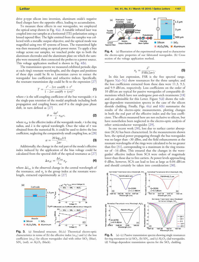
To measure these effects in our waveguides, we employedthe optical setup shown in Fig. 4(a). A tunable infrared laser wascoupled into our samples at a horizontal (TE) polarization using alensed tapered fiber. The light emitted from the samples was col-lected with a metallic output objective, and the optical mode wasmagnified using two 4F systems of lenses. The transmitted lightwas then measured using an optical power meter. To apply a biasvoltage across our samples, we touched probe tips to both thealuminum electrodes and the aluminum plate on which the sam-ples were mounted, then connected the probes to a power source.This voltage application method is shown in Fig. 4(b).
The transmission spectra we measured exhibited periodic dipsat each ring’s resonant wavelengths, and the shapes and positionsof these dips could be fit to Lorentzian curves to extract thewaveguides’ loss coefficients and refractive indices. Specifically,the resonant transmission dip could be fit to the expression [27]
T � t2 − 2tτ cos�θ� � τ2
1 − 2tτ cos�θ� � �tτ�2 ; (1)
where t is the self-coupling coefficient of the bus waveguide; τ isthe single-pass retention of the modal amplitude including bothpropagation and coupling losses; and θ is the single-pass phaseshift, in turn defined as [27]
θ � 4π2
λneff r; (2)
where neff is the effective index of the waveguide mode, r is the ringradius, and λ is the optical wavelength. Once the value of τ wasobtained from the numerical fit, it could be used to derive the losscoefficient, neglecting the comparatively small coupling loss, as [28]
α � 20 log10�τ�2πr
: (3)
Additionally, the change in the real part of the mode’s effectiveindex induced by the application of the bias voltage could becalculated from the spectral shift of the optical resonance as [27]
Δneff �Δλresλres
ng ; (4)
where Δλres is the observed change in the central wavelength ofthe resonance, and ng is the group index at the resonant wave-length, extracted experimentally as [27]
ng �λ2
FSR�2πr� : (5)
In this last expression, FSR is the free spectral range.Figures 5(a)–5(c) show resonances for the three samples; andthe loss coefficients extracted from these data were 11.3, 9.3,and 9.9 dB/cm, respectively. Loss coefficients on the order of10 dB/cm are typical for passive waveguides of comparable di-mensions which have not undergone post-etch treatments [18]and are admissible for this Letter. Figure 5(d) shows the volt-age-dependent transmission spectra in the case of the silicondioxide cladding. Finally, Figs. 6(a) and 6(b) summarize theresults of the electro-optic measurements, plotting changesin both the real part of the effective index and the loss coeffi-cient. The effects measured here are not exclusive to silicon, buthave nonetheless been neglected in the electro-optic analysis ofother semiconductor waveguides [29].
In one recent work [30], loss due to surface carrier absorp-tion (SCA) has been characterized. In the measurements shownhere, the optical power propagating through the bus waveguideswas no larger than −30 dBm, and the field enhancements at theresonant wavelengths of the rings were calculated to be no greaterthan five [31], corresponding to a maximum in the ring resona-tor of −16 dBm. This ensured that the changes in the wave-guides’ effective indices from SCA were orders of magnitudelower than those due to free carriers. At power levels approaching0 dBm, however, SCA can lead to loss as large as 0.04 dB/cmand should certainly be taken into consideration [30].
Fig. 3. (a) Simulated structure. (b),(c) Theoretical electro-opticcharacteristics in terms of (b) the effective index (nTE) and (c) the losscoefficient (αTE) for silicon waveguides clad with either SiO2 (blue),SiNx (red), or Al2O3 (black).
Fig. 4. (a) Illustration of the experimental setup used to characterizethe electro-optic properties of our fabricated waveguides. (b) Crosssection of the voltage application method.
Fig. 5. (a)−(c) Passive transmission spectra showing single resonancesfor ring resonators in (a) SiO2, (b) SiNx , and (c) Al2O3 clad waveguides.(d) Voltage-dependent transmission spectra for the SiO2 cladding.
Letter Vol. 41, No. 6 / March 15 2016 / Optics Letters 1187

The obtained results generally agree with the theoreticallyproduced values, although the magnitudes of both the electro-optic effects were larger than predicted. This is potentially dueto changes in the values of the fixed charge of the fabricatedsamples, resulting from the processing steps the silicon wave-guides’ surfaces were subjected to. These discrepancies mayadditionally have arisen from uncertainties in (1) the interfacetrap density at the silicon–dielectric interfaces, (2) the relevantindices of refraction, or (3) the dissimilar values of fixed chargebetween the upper wall and the sidewalls of the silicon wave-guide, due to the different set of processes they were subjectedto. Finally silicon nitride films deposited on silicon have beenshown to possess values of fixed charge which change in re-sponse to bias voltages, and this may explain why the electro-refractive response for the nitride clad waveguides was particu-larly large [32]. The overall trend, nonetheless, holds betweentheory and experiment, and the aforementioned uncertaintieschange only the magnitude of the measured effect, not the sign.Most notably, both the electro-optic effects change direction inthe case of Al2O3 due to its negative fixed charge, confirmingthat the effects seen here are due to free-carrier plasma dispersion.
Although the voltages required to characterize the presentdevices were large, there are several techniques, such as theuse of SOI wafers with thinner buried oxide layers, which allowthem to be reduced. Most promising, it is possible to switch to arib waveguide topology in which the silicon device layer servesas the grounding layer, and this is expected to yield a large en-hancement to the electro-optic effect.
In conclusion, we have shown how different dielectric clad-dings impact the capacitively induced electro-optic effect insilicon waveguides. These results are significant because theyclearly indicate how the capacitively induced free-carrier effectin waveguides with properly chosen cladding materials may beleveraged to realize CMOS-compatible electro-optic modula-tors and wavemixers which do not rely on the injection of elec-trical currents. Additionally, this Letter demonstrates that adielectric-clad silicon waveguide’s optical losses may be reducedor increased by applying an appropriately chosen bias voltage,allowing for the in vivo tuning and optimization of a wide vari-ety of photonic devices.
†These authors contributed equally.
Funding. National Science Foundation (NSF); DefenseAdvanced Research Projects Agency (DARPA); NSF ERCCIAN; Office of Naval Research (ONR); MultidisciplinaryUniversity Research Initiative (MURI); Cymer corporation.
REFERENCES
1. C. Malgrange, C. Ricolleau, and M. Schlenker, Symmetry andPhysical Properties of Crystals (Springer, 2014).
2. L. Pavesi and D. Lockwood, Silicon Photonics (Springer, 2004).3. G. Reed, G. Mashanovich, F. Gardes, and D. Thomson, Nat.
Photonics 4, 518 (2010).4. Q. Xu, B. Schmidt, S. Pradhan, and M. Lipson, Nature 435, 325 (2005).5. M. Cazzanelli, F. Bianco, E. Borga, G. Pucker, M. Ghulinyan, E.
Degoli, E. Luppi, V. Veniard, S. Ossicni, D. Modotto, S. Wabnitz,R. Pierobon, and L. Pavesi, Nat. Mater. 11, 148 (2012).
6. P. Damas, X. Le Roux, D. Le Bourdais, E. Cassan, D. Marris-Morini,N. Izard, T. Maroutian, P. Lecoeur, and L. Vivien, Opt. Express 22,22095 (2014).
7. M. Puckett, J. Smalley, M. Abashin, A. Grieco, and Y. Fainman, Opt.Lett. 39, 1693 (2014).
8. R. Jacobsen, K. Andersen, P. Borel, J. Fage-Pedersen, L. Frandsen,O. Hansen, M. Kristensen, A. Lavrinenko, G. Moulin, H. Ou, C.Peucheret, B. Zsigri, and A. Bjarklev, Nature 441, 199 (2006).
9. B. Chmielak, M. Waldow, C. Matheisen, C. Ripperda, J. Bolten, T.Wahlbrink, M. Nagel, F. Merget, and H. Kurz, Opt. Express 19,17212 (2011).
10. B. Chmielak, C. Matheisen, C. Ripperda, J. Bolten, T. Wahlbrink, M.Waldow, and H. Kurz, Opt. Express 21, 25324 (2013).
11. S. Azadeh, F. Merget, M. Nezhad, and J. Witzens, Opt. Lett. 40, 1877(2015).
12. R. Sharma, M. Puckett, H. Lin, F. Vallini, and Y. Fainman, Appl. Phys.Lett. 106, 241104 (2015).
13. A. Liu, R. Jones, L. Liao, D. Samara-Rubio, D. Rubin, O. Cohen, R.Nicolaescu, and M. Paniccia, Nature 427, 615 (2004).
14. M. Webster, P. Gothoskar, V. Patel, D. Piede, S. Anderson, R.Tunnidi, D. Adams, C. Appel, P. Metz, S. Sunder, B. Dama, and K.Shastri, in IEEE 11th International Conference on Group IVPhotonics (2014), pp. 1–2.
15. X. Chen, Y. Chen, Y. Zhao, W. Jiang, and R. Chen, Opt. Lett. 34, 602(2009).
16. L. Alloatti, C. Koos, and J. Leuthold, Appl. Phys. Lett. 107, 031107(2015).
17. C. Schriever, F. Bianco, M. Cazzanelli, M. Ghulinyan, C.Eisenschmidt, J. de Boor, A. Schmid, J. Heitmann, L. Pavesi, andJ. Schilling, Adv. Opt. Mater. 3, 129 (2015).
18. D. Sparacin, S. Spector, and L. Kimerling, J. Lightwave Technol. 23,2455 (2005).
19. Lumerical Solutions, Inc. http://www.lumerical.com/tcad‑products/fdtd/.20. Silvaco, Inc. http://www.silvaco.com/.21. M. Puckett, F. Vallini, A. Grieco, and Y. Fainman, Opt. Lett. 40, 379
(2015).22. R. Devine, J. Appl. Phys. 92, 3162 (2002).23. R. Kotipalli, R. Delamare, O. Poncelet, X. Tang, L. Francis, and D.
Flandre, EPJ Photovoltaics 4, 45107 (2013).24. T. Takakura, R. Imai, Y. Okamoto, and H. Taniguchi, Jpn. J. Appl.
Phys. 49, 046502 (2010).25. M. Nedeljkovic, R. Soref, and G. Mashanovich, IEEE Photon. J. 3,
1171 (2011).26. L. Alloatti, M. Lauermann, C. Surgers, C. Koos, W. Freude, and J.
Leuthold, Appl. Phys. Lett. 103, 051104 (2013).27. W. Bogaerts, P. De Heyn, T. Van Vaerenbergh, K. De Vos, S.
Selvaraja, T. Claes, P. Dumon, P. Bienstman, D. Van Thourhout,and R. Baets, Laser Photon. Rev. 6, 47 (2012).
28. J. Niehusmann, A. Vörckel, P. H. Bolivar, T. Wahlbrink, W. Henschel,and H. Kurz, Opt. Lett. 29, 2861 (2004).
29. C. Xiong, W. Pernice, and H. Tang, Nano Lett. 12, 3562 (2012).30. S. Grillanda and F. Morichetti, Nat Commun. 6, 8182 (2015).31. S. Keyvaninia, M. Karvar, and A. Bahrampour, Proc. SPIE 6996,
69961X (2008).32. M. Bazilchuk, H. Haug, and E. Marstein, Appl. Phys. Lett. 106, 143505
(2015).
Fig. 6. Electro-optic characteristics in terms of (a) the effective index(nTE) and (b) the loss coefficient (αTE) for waveguides clad with eitherSiO2 (blue), SiNx (red), or Al2O3 (black).
1188 Vol. 41, No. 6 / March 15 2016 / Optics Letters Letter