effect of metal overhang on electric field for pixel sensors kavita lalwani, geetika jain, ranjeet...
TRANSCRIPT

Effect of Metal Overhang on Electric Field for Pixel Sensors
Kavita Lalwani, Geetika Jain, Ranjeet Dalal, Kirti Ranjan & Ashutosh Bhardwaj Department of Physics & Astrophysics, University of Delhi, INDIA
SIMULATION GROUP MEETING13 January, 2015Delhi, India
SIMULATION GROUP MEETING13 January, 2015Delhi, India
Simulation Group Meeting, 23/1/2015
1

Simulated Structure for pixel sensor (three Pixel)
D=
200
um
2
xyz=1002001 um3
3 Pixel StructureBulk Type = BoronBulk Density = 21012cm-3
Bulk profile=constant Aluminium=0.55umGate SiO2=0.25um Field SiO2 = 0.7um Areafactor = NIL2 Contact Vias
Parameters Used Frontside Implant Type = PhosphorusFrontside Implant Density = 11019cm-3
Frontside Implant Profile = Gaussian,y=1.5um, x=1.05um
Backside Implant Type = BoronBackside Implant Density = 11019cm-3
Backside Implant Profile = Gaussian,y=1.5um, x=1.05um
Pstop density = 11016cm-3
Pstop implant profie= Gaussian, y=1.0um, x= 0.7um
Configuration-Pstop, implant wide
Metal overhang = 0, 4umT=253K
For Non Irradiated Pixels-Qf=1e11cm-2 + 2Nit traps [1]
For Irradiated Pixels- Radiation Damage Model=2bulktraps + Qf +2Nit traps [2]Qf= 2e12cm-2
Fluence = 0 (Non irradiated case), 1e15, 2e15, 5e15, 1e16cm-2
References-[1] Dissertation , “X ray Radiation damage studies and Design of a silicon pixel sensors for science at the XFEL, by Jiaguo Zhang, 2013.[2] “Simulation of Irradiated Si Detectors”, Ranjeet Dalal et al, Proceeding of Vertex 2014
2]

2D Electric Field Profiles for Non Irradiated Pixel SensorsConfiguration-Pstop, implant wide
MO=0um MO=4um
Maximum electric field is at the curvature ofn+ strips
3
Applied reverse bias = 1000V
Maximum electric field is under the MO
It is expected that effect of MO would be significant for non irradiated pixel sensors
N+ implant
No Metal overhang
P Bulk
N+ implant
Metal overhang
P Bulk
N+ implant

Cutline of 1umCutline of 0.1 um
Non irradiated pixel sensors
MO has significant effect on maximum electric field for non-irradiated pixel sensors.
There is decrease in maximum electric field for MO of 4um compared to structure without MO.
Applied reverse bias = 1000V
MO effect on Electric Field
Gap bw pstop
Implant edge Implant edge
Gap bw pstop
implant pstop edge implant pstop edge
4

2D Electric Field Profile for Irradiated Pixel Sensors Configuration-Pstop, implant wide
MO = 4umMO = 0um
Maximum electric field is at the curvature of n+ strips It is expected that effect of MO would not be very significant for irradiated pixel sensors 5
Applied reverse bias =1000V
fluence = 2e15cm-2
Qf=2e12cm-2
No Metal overhang
n+ implant
P bulk
fluence = 2e15cm-2
n+ implant
P bulk
Metal overhang
fluence = 2e15cm-2
Qf=2e12cm-2
Irradiated Pixel sensors
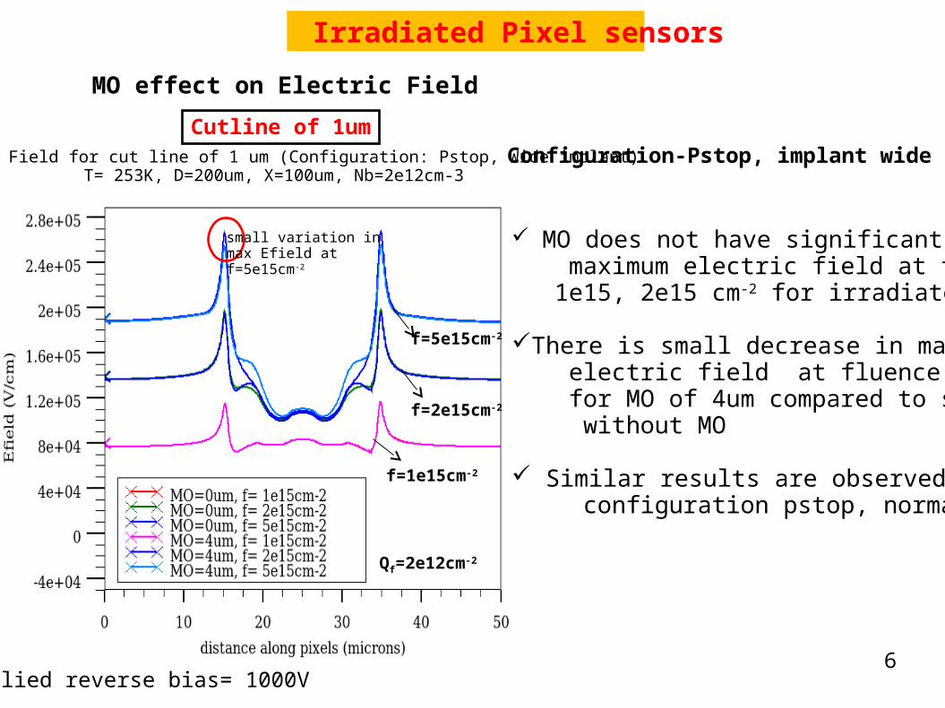
Electric Field for cut line of 1 um (Configuration: Pstop, Wide implant)T= 253K, D=200um, X=100um, Nb=2e12cm-3
Configuration-Pstop, implant wide
6Applied reverse bias= 1000V
MO effect on Electric Field
MO does not have significant effect on maximum electric field at fluences of 1e15, 2e15 cm-2 for irradiated pixel sensors.
There is small decrease in maximum electric field at fluence of 5e15 cm-2 for MO of 4um compared to structure without MO
Similar results are observed for configuration pstop, normal implant
small variation inmax Efield at f=5e15cm-2
Cutline of 1um
Qf=2e12cm-2
f=1e15cm-2
f=2e15cm-2
f=5e15cm-2
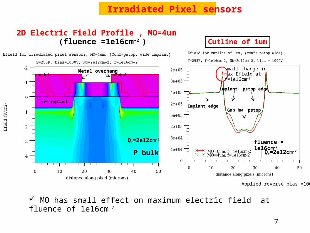
MO has small effect on maximum electric field at fluence of 1e16cm-2
7
Applied reverse bias =1000V
Irradiated Pixel sensors
small change inmax Efield at f=1e16cm-2
implant pstop edge
Gap bw pstopImplant edge
Cutline of 1um2D Electric Field Profile , MO=4um (fluence =1e16cm-2 )
Qf=2e12cm-2
fluence = 1e16cm-2
Metal overhang
P bulk
Qf=2e12cm-2
n+ implant

8
Fluences (cm-2) MO=0um MO=4um MO=0um MO=4um
f=0 (Non irradiated case)
1.72105 1.33105 1.81105 9.82104
f=1e15 1.14105 1.14105 1.09105 1.09105
f=2e15 1.97105 1.94105 1.35105 1.43105
f=5e15 2.67105 2.55105 1.46105 1.64105
f=1e16 3.09105 2.93105 1.78105 1.76105
Cutline=1um
Configuration- Pstop, implant wide
Cutline=0.1um
Comparison of Maximum Electric Field (Non Irradiated vs Irradiated Pixel Sensors)
Applied reverse bias = 1000V
Electric field unit V/cm

9
Summary
Electric field simulations are performed to study the effect of metal overhang for both non irradiated as well irradiated pixel sensors.
-For Non irradiated pixel senors MO has a significant effect on maximum electric field
- For irradiated pixel senors MO does not have significant effect on maximum electric field at fluences of 1e15, 2e15 cm-2
There is small decrease in maximum electric field at fluence of 5e15 cm-2 and 1e16cm-2
for MO of 4um compared to structure without MO Similar results are observed for configuration pstop, normal implant
Future Plan
Study the effect of various design parameters like pstop depth, pstop concentration, effective doping concentration etc on electric field profiles for non irradiated and irradiated pixel sensorsStudy the design optimization for the pixel structures- 1) X (width)=50um & depth =200um 2)X (width) = 25um & depth = 200um

10
Thank you

Back-up Slides
11

12
Electric Field in Bulk
Irradiated pixel sensors at f=1e15cm-2
Non IrrNon Irradiated pixel sensors at QF=1e11cm-2 + interface trap

Conf-Pstop, Implant Wide (cutline of 1.0um)
MO Effect on Electric Field at different fluences for Irradiated Strip sensors
13
Fluence = 1e15cm-2
Fluence = 2e15cm-2
Fluence = 5e15cm-2
Fluence = 1e16cm-2

14
MO Effect on Electric Field at different fluences for Irradiated Strip sensors
Conf-Pstop, Implant Wide (cutline of 0.1um)
f=1e15cm-22f=2e15cm-22
f=5e15cm-22 f=1e16cm-22
15
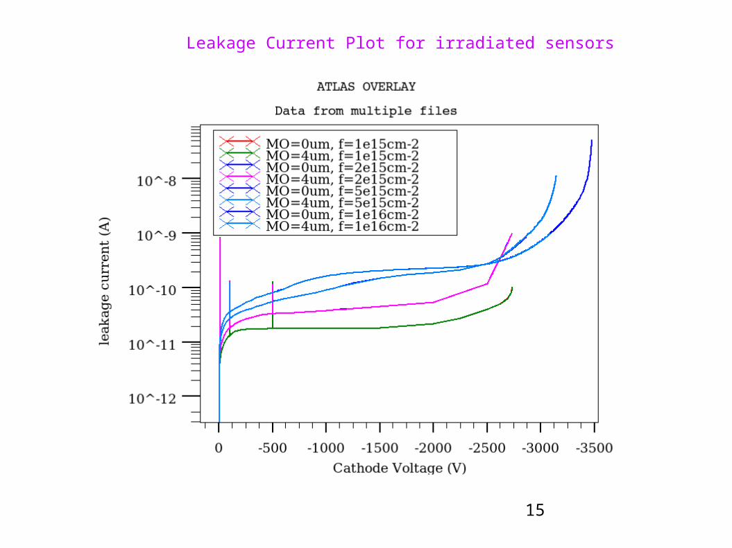
Leakage Current Plot for irradiated sensors

16
Net Doping, f= 1e16, MO=4um
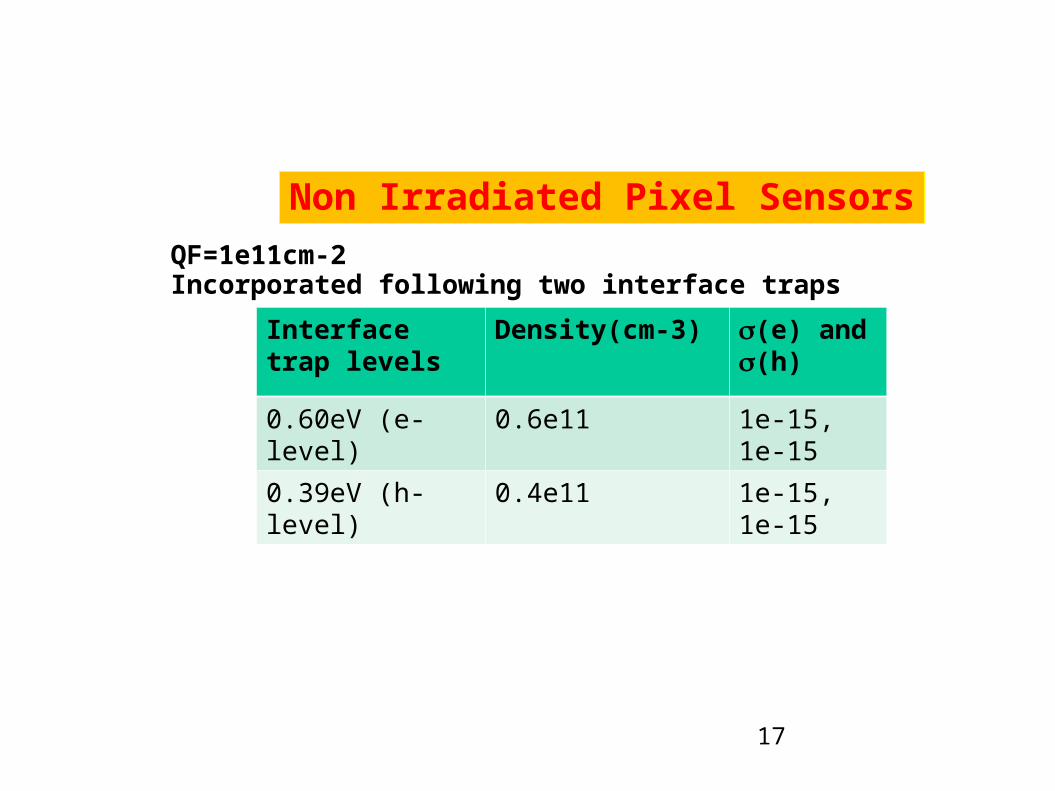
Non Irradiated Pixel Sensors
QF=1e11cm-2Incorporated following two interface traps
Interface trap levels
Density(cm-3) (e) and (h)
0.60eV (e-level) 0.6e11 1e-15, 1e-15
0.39eV (h-level) 0.4e11 1e-15, 1e-15
17

Irradiated Pixel Sensors
18
Fixed interface charge density (QF) =2e12cm-2
Incorporated following two interface traps
Interface trap levels
Density(cm-3) (e) and (h)
0.60eV (e-level) 12e11 1e-15, 1e-15
0.39eV (h-level)
8e11 1e-15, 1e-15
trap levels Density(cm-3) at f=1e15,2e15,5e15cm-2
(e) and (h)
0.51eV (e-level) 4e15, 8e15,2e16 2e-14, 2.6e-14
0.48eV (h-level)
3e15,6e15,1.5e16 2e-14, 2e-14
Bulk Damage Model