elec4614 power electronics protection of power … 24...elec4614 power electronics lecture 24 –...
TRANSCRIPT

ELEC4614 Power Electronics
Lecture 24 – Thermal Design 1 F. Rahman
Protection of Power Electronic Switching Devices
1. Voltage and current stresses
Snubber Circuits
Purpose:
1. To keep the operation of the switch within its safe operating area. These limits relate to the maximum voltage and current stresses of switches.
2. To keep the di
dt and
dv
dt in or across certain
switches within allowable limits.
3. To contain the power loss of the switch within safe limits by adjusting the turn-on and turn-off transients of switches.
4. Power transistors (MOSFET, BJT, IGBT) normally have safe operating areas defined by their maximum current voltage and power dissipation boundaries, as indicated by the red envelop in the figure 24.1.

ELEC4614 Power Electronics
Lecture 24 – Thermal Design 2 F. Rahman
Figure 24.1
Careful examination of the voltage-current trajectories of a diode-clamped circuit (the most common) will show that the v-i trajectories at turn-on and turn-off follow the dotted path. Ideally, such paths should be along the axes, as indicated by the blue lines. Snubber circuits help operation close to the ideal paths.
ELEC4614 Power Electronics
Lecture 24 – Thermal Design 3 F. Rahman
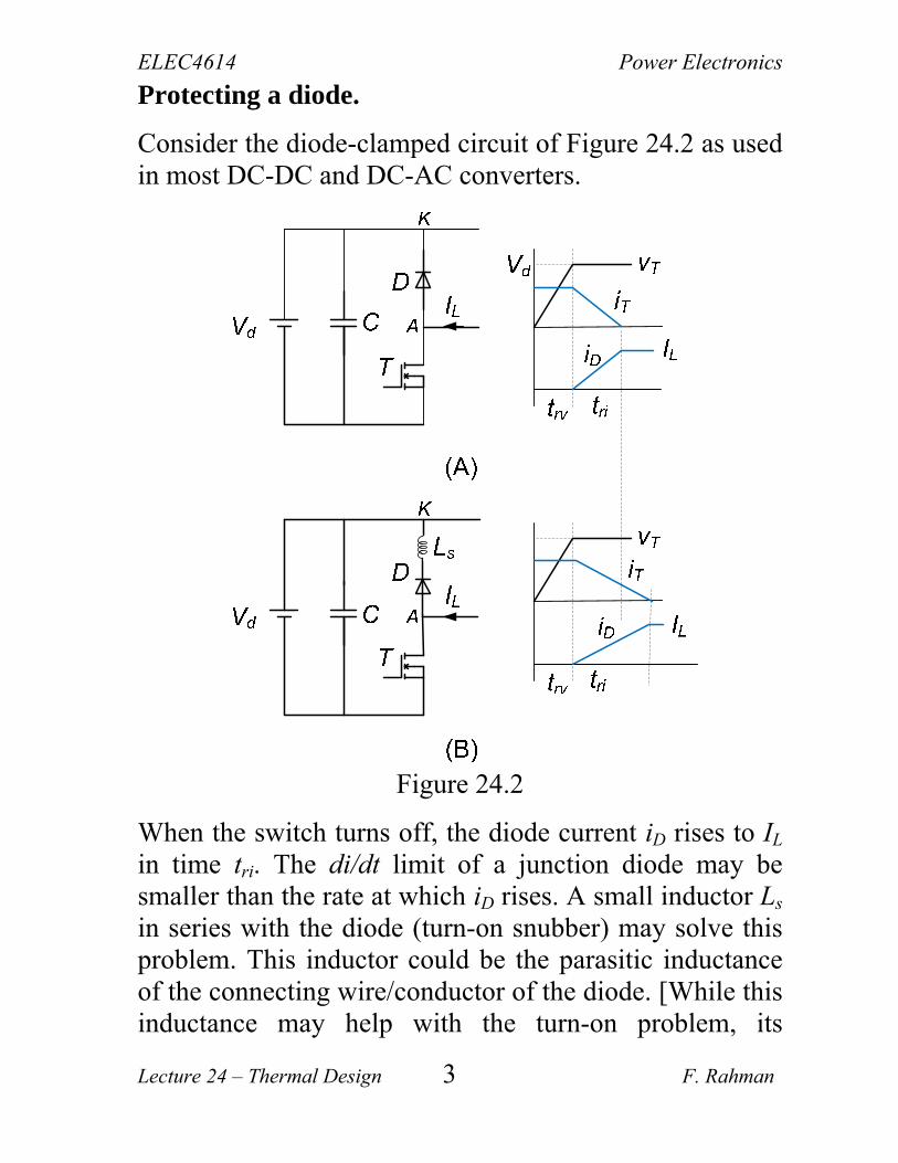
Protecting a diode.
Consider the diode-clamped circuit of Figure 24.2 as used in most DC-DC and DC-AC converters.
Figure 24.2
When the switch turns off, the diode current iD rises to IL in time tri. The di/dt limit of a junction diode may be smaller than the rate at which iD rises. A small inductor Ls in series with the diode (turn-on snubber) may solve this problem. This inductor could be the parasitic inductance of the connecting wire/conductor of the diode. [While this inductance may help with the turn-on problem, its

ELEC4614 Power Electronics
Lecture 24 – Thermal Design 4 F. Rahman
presence creates an overvoltage problem at turn off. Because of this, the C-D-T circuit is normally as compact as possible].
Example 24.1
During turn-on of the switch T in Figure 2(A), the diode current falls at a rate largely given by Vd/Ls, where Ls is the parasitic inductance Ls of the C-D-T circuit. This rate of fall of diode current also determines the peak reverse recovery current of the diode. Assuming that the peak reverse current of the diode (Irr) reaches 60A and the diode snap-off time (ts) is 10 nsec, what is the peak voltage VT across the switch due to the diode turning off? Given: Vd = 50V and Ls = 12 nH.
Answer:
di/dt = 60/10 nsec = 6×10⁹ A/sec.
Peak voltage VT = Vd + Ls×di/dt
= 50 + 12×109 × 6×109 = 112 V
This implies that the peak voltage rating of the switch must be higher than 112V! Cleary, the C-D-T loop inductance of 12 nH is too high.
ELEC4614 Power Electronics
Lecture 24 – Thermal Design 5 F. Rahman
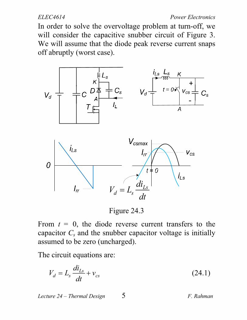
In order to solve the overvoltage problem at turn-off, we will consider the capacitive snubber circuit of Figure 3. We will assume that the diode peak reverse current snaps off abruptly (worst case).
Lsd s
diV L
dt
Figure 24.3
From t = 0, the diode reverse current transfers to the capacitor Cs and the snubber capacitor voltage is initially assumed to be zero (uncharged).
The circuit equations are:
Lsd s cs
diV L v
dt (24.1)

ELEC4614 Power Electronics
Lecture 24 – Thermal Design 6 F. Rahman
csLs s
dvi C
dt (24.2)
Solving equations (1) and (2) with initial conditions: iLs(0) = Irr and vcs(0) = 0,
scs d d o rr o
s
Lv V V cos t I sin t
C (24.3)
where os s
1
L C rad/sec. (24.4)
We will introduce a base-line capacitance given by equating
2 2s rr b d
1 1L I C V
2 2 , so that
2
rrb s
d
IC L
V
(24.5)
Thus,
bcs d o o
s
Cv V 1 cos t sin t
C
(24.6)
The maximum capacitor (or switch voltage) is given by
ELEC4614 Power Electronics
Lecture 24 – Thermal Design 7 F. Rahman
bcs max d
s
CV V 1 1
C
(24.7)
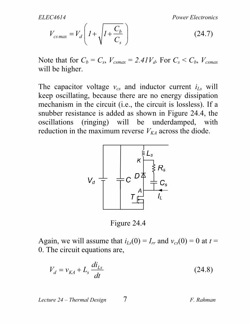
Note that for Cb = Cs, Vcsmax = 2.41Vd. For Cs < Cb, Vcsmax will be higher. The capacitor voltage vcs and inductor current iLs will keep oscillating, because there are no energy dissipation mechanism in the circuit (i.e., the circuit is lossless). If a snubber resistance is added as shown in Figure 24.4, the oscillations (ringing) will be underdamped, with reduction in the maximum reverse VKA across the diode.
Figure 24.4
Again, we will assume that iLs(0) = Irr and vcs(0) = 0 at t = 0. The circuit equations are,
Lsd KA s
diV v L
dt (24.8)
ELEC4614 Power Electronics
Lecture 24 – Thermal Design 8 F. Rahman
csLs s
dvi C
dt (24.9)
KA s Ls csv R i v (24.10) From 24.10,
2 22
cs LsKAs2 2 2
d v d id vR
dt dt dt
From 24.8,
22
LsKAd s s s KA2 2
d id vV L C R v
dt dt
(24.11)
Now, 2
Ls Ls2
d i did
dt dtdt
2
LsKAd s s s KA2
did v dV L C R v
dt dtdt
2
KAs s s s s d KA KA2
s
d v d 1L C L C R V v v
dt Ldt
2
KA KAs s s s KA2
d v dvL C C R v
dtdt (24.12)
Thus, 2
KA KAs s s s KA d2
d v dvL C C R v V
dtdt (24.13)
ELEC4614 Power Electronics
Lecture 24 – Thermal Design 9 F. Rahman
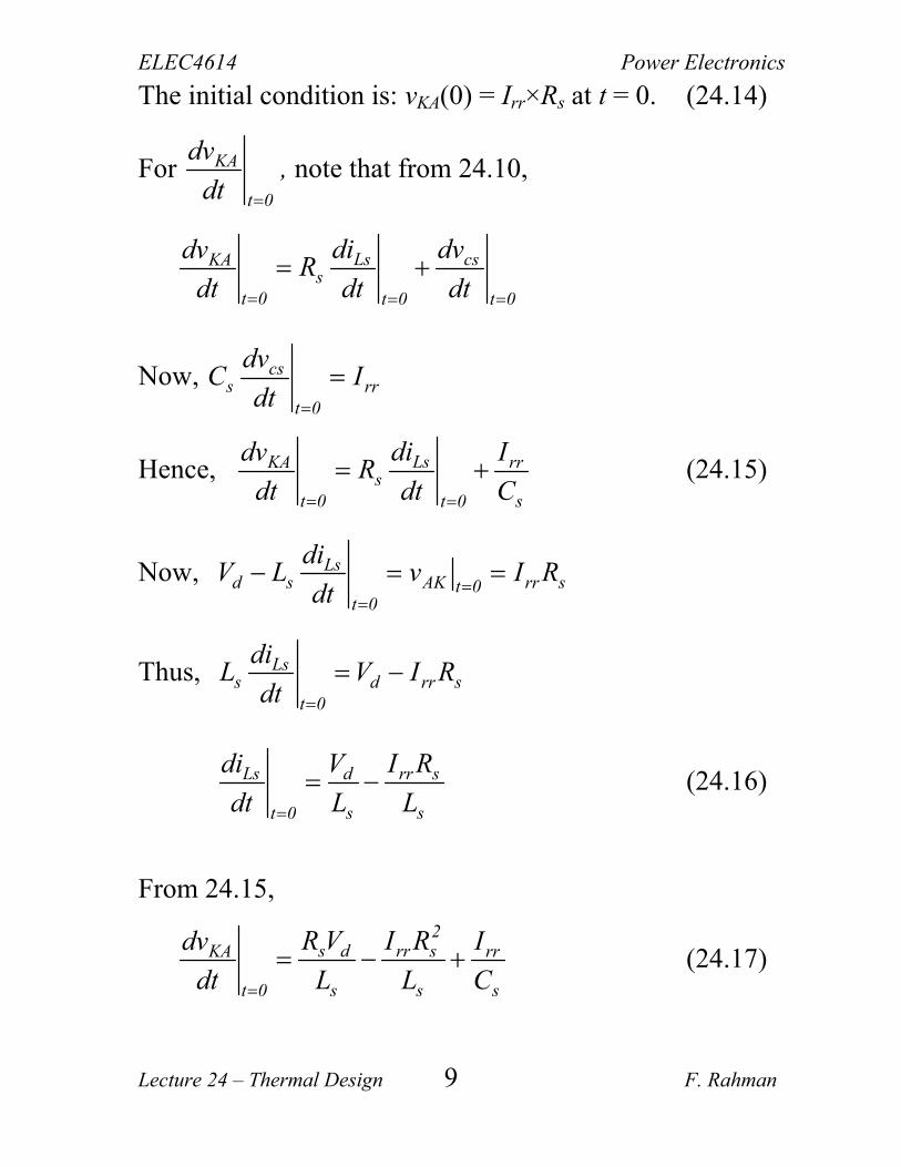
The initial condition is: vKA(0) = Irr×Rs at t = 0. (24.14)
For KA
t 0
dv,
dt
note that from 24.10,
Ls csKAs
t 0 t 0 t 0
di dvdvR
dt dt dt
Now, css rr
t 0
dvC I
dt
Hence, LsKA rrs
t 0 st 0
didv IR
dt dt C
(24.15)
Now, Lsd s AK rr st 0
t 0
diV L v I R
dt
Thus, Lss d rr s
t 0
diL V I R
dt
Ls d rr s
s st 0
di V I R
dt L L
(24.16)
From 24.15,
2s d rr sKA rr
t 0 s s s
R V I Rdv I
dt L L C
(24.17)

ELEC4614 Power Electronics
Lecture 24 – Thermal Design 10 F. Rahman
Solution of 24.13 subject to boundary conditions 24.14 and 24.17 is given by,
ts rrKA d
s
L Iv V e cos t
C cos
(24.18)
where
2 2o
2o
, the damped natural frequency.
sR
2
, the attenuation rate.
1 d rr s
s rr
V I R / 2tan
L I
1tan
Note that vKA = Vd for t = , when oscillations have died down. The time during which oscillations die out is (damping) and the peak VAK are determined by Rs.
A base-line value Rb for Rs can be defined as
db
rr
VR
I (24.19)

ELEC4614 Power Electronics
Lecture 24 – Thermal Design 11 F. Rahman
The normalised reverse voltage across the diode is plotted in figure 24.5 for various values of Rs and Cs = Cb defined by equation 24.5.
1
2
3
4
1 2 3 4
Rs/Rb
VKA/Vd
Figure 24.5
Note that for minimum VKA, Rs = 1.3×Rb.
Note also that the snubber circuit causes additional power loss. The energy loss in the snubber resistance is given by
2 2Rs s rr s d
1 1W L I C V
2 2 Joules (24.20)
This is the energy loss at the end of oscillations when the capacitor Cs is charged to Vd.

ELEC4614 Power Electronics
Lecture 24 – Thermal Design 12 F. Rahman
The energy stored in Cs is also dissipated when the diode turns on. Thus the total energy loss due to the snubber per cycle of switching is
2 2s tot s rr s d
1W L I C V
2 Joules (24.21)
The power loss when the diode operates with a switching frequency fs is given by
s tot s tot sP W f Watts (24.22)
The above analyses are easily applicable to other circuits as described below.

ELEC4614 Power Electronics
Lecture 24 – Thermal Design 13 F. Rahman
Snubber for the diode in the Flyback converter
Figure 24.6
Note that when the switch turns on, the reverse voltage across the diode which starts the reverse recovery process
is 2o d
1
NV V
N .
For non-isolated DC-DC converter and inverter circuits, the power circuit lay-out is made as compact as possible so that parasitic inductances are small. It is sometimes possible to avoid snubber components for the diodes in these converters.

ELEC4614 Power Electronics
Lecture 24 – Thermal Design 14 F. Rahman
Snubbers for isolated DC-DC converters
For push-pull, half- and full-bridge DC-DC converters, the leakage inductance in the secondary winding is usually large. With continuous conduction of inductor current, each secondary winding carries half of the load (filter inductor current) when the switches are off. When a switch turns on, a positive voltage, say (N2/N1)Vd, is applied across the one of the secondary windings, say with diode D1. The current in this diode and the filter inductor L increases as a result at the rate [(N2/N1)Vd
Vo]/L. During this time, the other secondary winding applies 2(N2/N1)Vd as reverse bias to diode D2. Note that the reverse recovery current of diode D2 flows through two leakage inductances in series. The circuits of Figure 24.7 indicate the converter for snubber analysis.
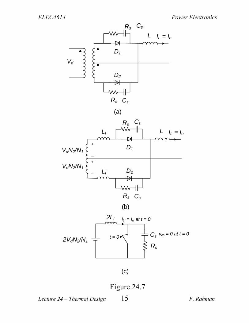
ELEC4614 Power Electronics
Lecture 24 – Thermal Design 15 F. Rahman
L
Rs Cs
Rs Cs
D1
D2
Vd
IL = Io
LRs Cs
Rs Cs
D1
D2
IL = IoLl
Ll
VdN2/N1
VdN2/N1
+
_
+
_
Rs
Cs2VdN2/N1
2Ll
t = 0vcs = 0 at t = 0
iLl = Irr at t = 0
(a)
(b)
(c)
Figure 24.7

ELEC4614 Power Electronics
Lecture 24 – Thermal Design 16 F. Rahman
Single-phase Bridge AC-DC Rectifier.
Figure 24.8

ELEC4614 Power Electronics
Lecture 24 – Thermal Design 17 F. Rahman
Three-phase diode AC-DC rectifier
Ls
Cf
vAn
vBn
vCn
Ls
Ls
2Ls
Vmax,l-lRs
Cs
(a)
(b)
Figure 24.9

ELEC4614 Power Electronics
Lecture 24 – Thermal Design 18 F. Rahman
Three-phase fully-controlled Thyristor converter
Ls
Cf
vAn
vBn
vCn
Ls
Ls
2Ls
Vmax,l-lRs
Cs
(a)
(b)
Figure 24.10
ELEC4614 Power Electronics
Lecture 24 – Thermal Design 19 F. Rahman
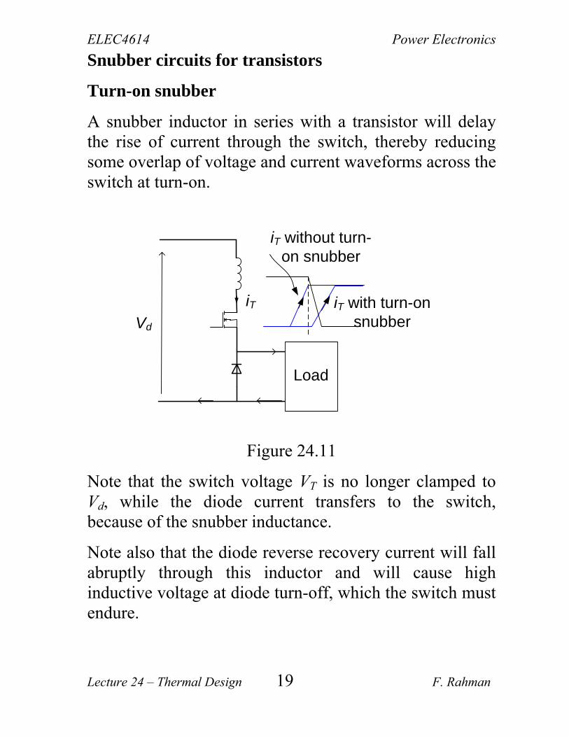
Snubber circuits for transistors
Turn-on snubber
A snubber inductor in series with a transistor will delay the rise of current through the switch, thereby reducing some overlap of voltage and current waveforms across the switch at turn-on.
Figure 24.11
Note that the switch voltage VT is no longer clamped to Vd, while the diode current transfers to the switch, because of the snubber inductance.
Note also that the diode reverse recovery current will fall abruptly through this inductor and will cause high inductive voltage at diode turn-off, which the switch must endure.
iT with turn-on snubber
iT without turn-on snubber
iT
LoadLoad
Vd
ELEC4614 Power Electronics
Lecture 24 – Thermal Design 20 F. Rahman
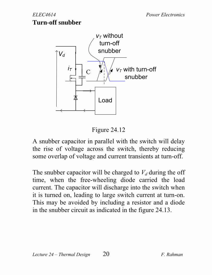
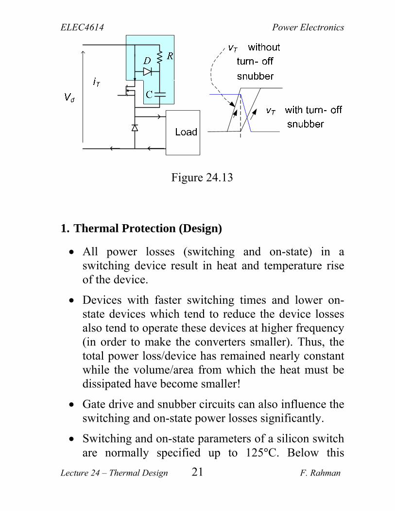
Turn-off snubber
Figure 24.12
A snubber capacitor in parallel with the switch will delay the rise of voltage across the switch, thereby reducing some overlap of voltage and current transients at turn-off.
The snubber capacitor will be charged to Vd during the off time, when the free-wheeling diode carried the load current. The capacitor will discharge into the switch when it is turned on, leading to large switch current at turn-on. This may be avoided by including a resistor and a diode in the snubber circuit as indicated in the figure 24.13.
ELEC4614 Power Electronics
Lecture 24 – Thermal Design 21 F. Rahman
Figure 24.13
1. Thermal Protection (Design)
All power losses (switching and on-state) in a switching device result in heat and temperature rise of the device.
Devices with faster switching times and lower on-state devices which tend to reduce the device losses also tend to operate these devices at higher frequency (in order to make the converters smaller). Thus, the total power loss/device has remained nearly constant while the volume/area from which the heat must be dissipated have become smaller!
Gate drive and snubber circuits can also influence the switching and on-state power losses significantly.
Switching and on-state parameters of a silicon switch are normally specified up to 125°C. Below this

ELEC4614 Power Electronics
Lecture 24 – Thermal Design 22 F. Rahman
temperature, the intrinsic carrier density can be assumed to be small compared to doped carrier density. Wide band-gap silicon carbide devices being announced recently allow switching devices to operate at about 600°C, reducing heat sink volume and weight significantly.
Mean Time between Failure (MTBF) halves for each 10°C rise of junction temperature above 50°C.
Heat dissipation by conduction
Figure 24.14
2 1d
SP
l
=
cR
(24.22)
where Pd is the total power loss in the switch.
l is the depth (length) of the heat-sink in m.
λ is the thermal conductivity in Watts/ m/ per °C.
S is the cross section area of the sink in m2.

ELEC4614 Power Electronics
Lecture 24 – Thermal Design 23 F. Rahman
The thermal resistance Rθc is defined as
cl
RS
in °C/W; (24.23)
so that c dR P (24.24)
Note the similarity of equation (24.24) with V = IR. Thus the power dissipation can be thought as a current flow which develops a temperature difference which is akin to potential difference of an electrical circuit. Note also that equation (24.24) refers to the DC or steady-state behaviour of the thermal circuit.
Table 24.1. Thermal conductivity of materials used in power switches
Material Thermal Conductivity W/m/C
Mylar 0.157 Silicone Grease 0.192 Mica 0.667 Alumina 16.67 Silicon 83.3Beryllia 100 Aluminum Nitrite 152.65 Aluminum 208.33 Copper 400
If there are more than one material between the junction and the surrounding area at the ambient temperature θa,

ELEC4614 Power Electronics
Lecture 24 – Thermal Design 24 F. Rahman
j d jc cs sa aP R R R (24.25)
Figure 24.15
Figure 24.16
j a d jc cs saP R R R (24.26)

ELEC4614 Power Electronics
Lecture 24 – Thermal Design 25 F. Rahman
Normally, j, a (25°C and 125°C, respectively), and Rθjc are pre-determined. Then Pd, Rθcs and Rθsa can be selected so that that j does not exceed 125°C for the highest Pd. Example 2:
Consider a switch in a TO-3 package. The maximum power dissipation is 25W. The following thermal resistances are present: Rθjc = 0.76, Rθcs = 0.12, Rθsa = 1.8, all in °C/W. Assuming the ambient temperature to be 40°C, find the sink, case and junction temperatures.
25 1.8 40 85sT C
25 0.12 85 88cT C 25 0.75 88 106.75jT C
Note that, 25 1.8 0.12 0.75 40 106.75jT C
What is the implication of including an isolating layer between the case and the sink?
ELEC4614 Power Electronics
Lecture 24 – Thermal Design 26 F. Rahman
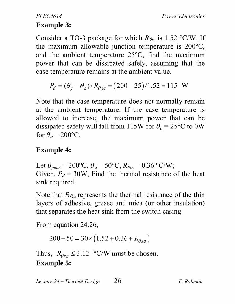
Example 3:
Consider a TO-3 package for which Rθjc is 1.52 °C/W. If the maximum allowable junction temperature is 200°C, and the ambient temperature 25°C, find the maximum power that can be dissipated safely, assuming that the case temperature remains at the ambient value.
( ) / 200 25 /1.52 115d j a jcP R W
Note that the case temperature does not normally remain at the ambient temperature. If the case temperature is allowed to increase, the maximum power that can be dissipated safely will fall from 115W for a = 25°C to 0W for a = 200°C.
Example 4:
Let jmax = 200°C, a = 50°C, Rθcs = 0.36 °C/W; Given, Pd = 30W, Find the thermal resistance of the heat sink required.
Note that Rθcs represents the thermal resistance of the thin layers of adhesive, grease and mica (or other insulation) that separates the heat sink from the switch casing.
From equation 24.26,
200 50 30 1.52 0.36 saR
Thus, 3.12saR °C/W must be chosen. Example 5:

ELEC4614 Power Electronics
Lecture 24 – Thermal Design 27 F. Rahman
Consider a power transistor which dissipates 100W with c = 25°C and j = 200°C. The Rθjc and Rθca are 1.4 and
27 °C/W, respectively. Find the maximum power which can be safely dissipated, and the case temperature, if no heat sink is used.
j c jc dR P (1)
c a ca dR P (2)
If the case temperature remained at 25°C/W, 100W would be dissipated. Adding (1) and (2)
200 25 jc ca dR R P
200 25
6.1627 1.4dP
W
From (1) or (2),
191.4c °C

ELEC4614 Power Electronics
Lecture 24 – Thermal Design 28 F. Rahman
The ambient temperature a of 25°C may be rather elusive. This is because a power converter circuit comprises a number of devices, transformers, capacitors, and inductors, all of which produce losses and hence increase the ambient temperature inside the converter enclosure within which these are located. These are also in close proximity in order to reduce parasitic inductances and the overall volume of the circuit. Note that forced (fan or water) cooling helps to keep the ambient temperature inside the enclosure close to the outside ambient temperature.
Rθsa decreases with forced cooling. Heat sink manufacturers provide Rθsa data for their sinks for various air or liquid flow rate in m3/sec maintained at certain specified temperature.
ELEC4614 Power Electronics
Lecture 24 – Thermal Design 29 F. Rahman
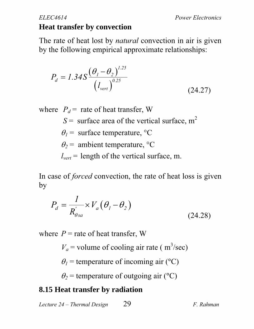
Heat transfer by convection
The rate of heat lost by natural convection in air is given by the following empirical approximate relationships:
1.25
1 2d 0.25
vert
P 1.34Sl
(24.27)
where Pd = rate of heat transfer, W
S = surface area of the vertical surface, m2
1 = surface temperature, °C
2 = ambient temperature, °C
lvert = length of the vertical surface, m.
In case of forced convection, the rate of heat loss is given by
d a 1 2'sa
1P V
R
(24.28)
where P = rate of heat transfer, W
Va = volume of cooling air rate ( m3/sec)
1 = temperature of incoming air (°C)
2 = temperature of outgoing air (°C)
8.15 Heat transfer by radiation

ELEC4614 Power Electronics
Lecture 24 – Thermal Design 30 F. Rahman
Rate of heat transfer by radiation is given by
4 41 2P kS
(24.29)
where P = rate of heat radiation, W
S = surface area, m2
1 = absolute temperature of body, °K
2 = absolute temperature of surroundings, °K
k = radiation constant which depends upon the nature of the body surface.
The radiation constant k varies from 80.2 10 W/(m2-°K4) for polished silver, to 85.7 10 W/(m2-°K4) for a perfect emitter (blackbody).

ELEC4614 Power Electronics
Lecture 24 – Thermal Design 31 F. Rahman
Dynamics of heat transfer – the thermal impedance
Because of storage of heat energy (in Joules) in a mass, the temperature of a body cannot change instantaneously. The stored energy in a mass m at a temperature °C is given by Q mc J (Joules) (24.30) where c = specific heat in J/kg-°C.
The rate of change of stored energy is the power input to the mass, which needs to be dissipated. Thus
d
dQ dP mc
dt dt
W
Consider that power dissipation of Pd (watts) results in some temperature rise. In time dt, the total energy loss is
Pdt. Some of this energy, 0
Sdt
l
, is dissipated to
the environment by conduction. Some is stored in the thermal mass. Neglecting dissipation in all other modes except conduction, the rest of the input energy, mcd, raises the temperature by d from an initial temperature θo in time dt. Thus,
d 0
SP dt mcd dt
l

ELEC4614 Power Electronics
Lecture 24 – Thermal Design 32 F. Rahman
d 0
d SP mc
dt l
d 0
d S Smc P
dt l l
(24.31)
Solving the first order differential equation,
St
mcl d0
P lCe
S
(24.32)
At t = 0 sec, we assume that 0 , so that
dl
C PS
(24.33)
St
mcld d0
P l P le
S S
St
mcld0
P l1 e
s
(24.34)
t /ss 1 e
(24.35)
ELEC4614 Power Electronics
Lecture 24 – Thermal Design 33 F. Rahman
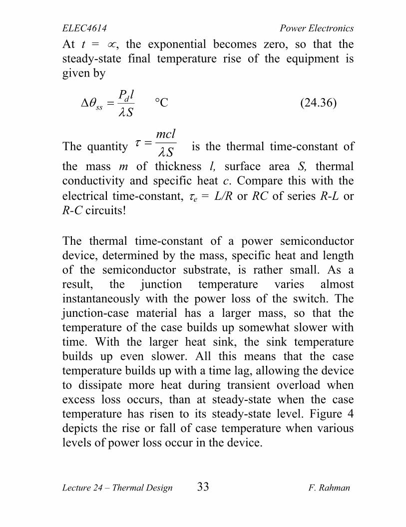
At t = , the exponential becomes zero, so that the steady-state final temperature rise of the equipment is given by
dss
P l
S
°C (24.36)
The quantity mcl
S
is the thermal time-constant of
the mass m of thickness l, surface area S, thermal conductivity and specific heat c. Compare this with the electrical time-constant, e = L/R or RC of series R-L or R-C circuits!
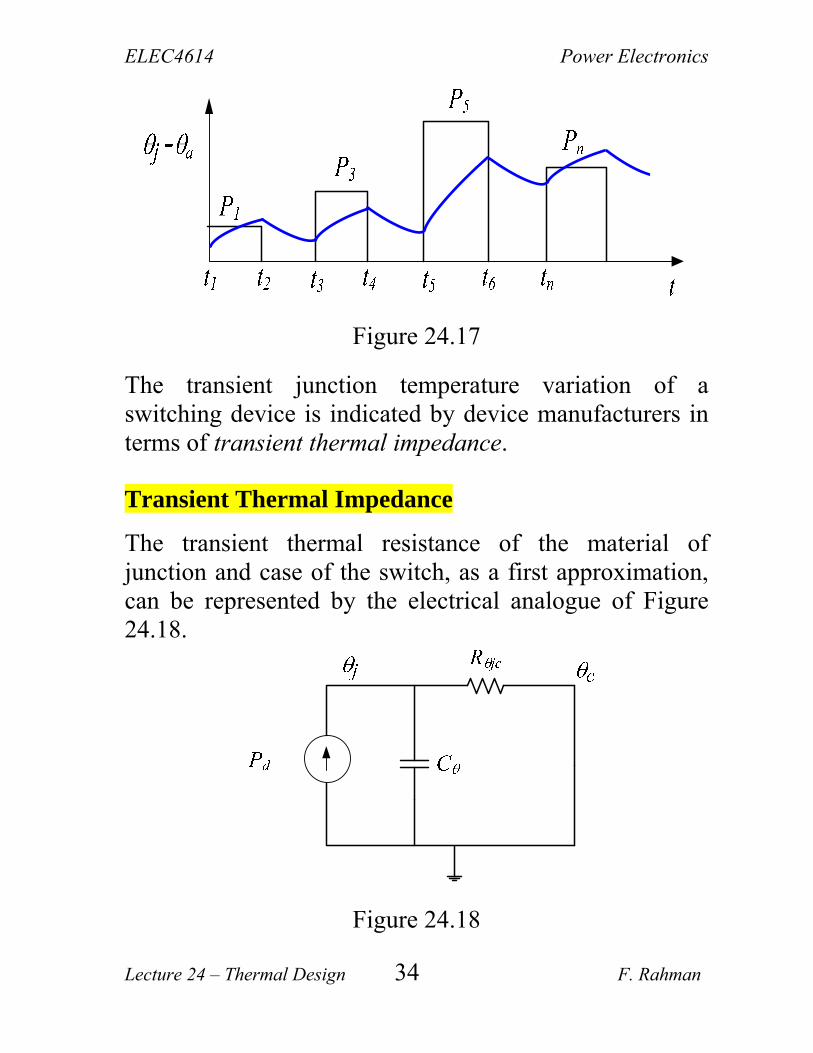
The thermal time-constant of a power semiconductor device, determined by the mass, specific heat and length of the semiconductor substrate, is rather small. As a result, the junction temperature varies almost instantaneously with the power loss of the switch. The junction-case material has a larger mass, so that the temperature of the case builds up somewhat slower with time. With the larger heat sink, the sink temperature builds up even slower. All this means that the case temperature builds up with a time lag, allowing the device to dissipate more heat during transient overload when excess loss occurs, than at steady-state when the case temperature has risen to its steady-state level. Figure 4 depicts the rise or fall of case temperature when various levels of power loss occur in the device.
ELEC4614 Power Electronics
Lecture 24 – Thermal Design 34 F. Rahman
Figure 24.17
The transient junction temperature variation of a switching device is indicated by device manufacturers in terms of transient thermal impedance.
Transient Thermal Impedance
The transient thermal resistance of the material of junction and case of the switch, as a first approximation, can be represented by the electrical analogue of Figure 24.18.
Figure 24.18

ELEC4614 Power Electronics
Lecture 24 – Thermal Design 35 F. Rahman
Here, Cθ = mc, is a capacitance which represents the thermal mass m and specific heat c of case material. The first-order equation representing this circuit, where Cθ represents the thermal mass of the switch, which includes the case, is
j j ad
jc jc
dC P
dt R R
(24.37)
Solving (24.37), with the assumption that j a at t = 0,
/1 tj jc d aR P e
(24.38)
where τ = Rθjc×C mcl
S, the junction-case thermal
time-constantin seconds. The junction temperature rises exponentially to 63.2% of its final value in time τ. When t
≈ 4τ, the junction temperature reaches the steady-state value
j jc d aR P (24.39)
The quantity /1 tjcZ t R e
is the transient
thermal impedance of the switch.

ELEC4614 Power Electronics
Lecture 24 – Thermal Design 36 F. Rahman
Figure 24.19 When there are several layers of material which Pd must flow through, including the heat sink, the equivalent circuit of figure 24.20 applies.
Figure 24.20
For n thermal masses,
/
1
( ) 1n
t ith i
i
Z t R e
ELEC4614 Power Electronics
Lecture 24 – Thermal Design 37 F. Rahman
where i i iR C .
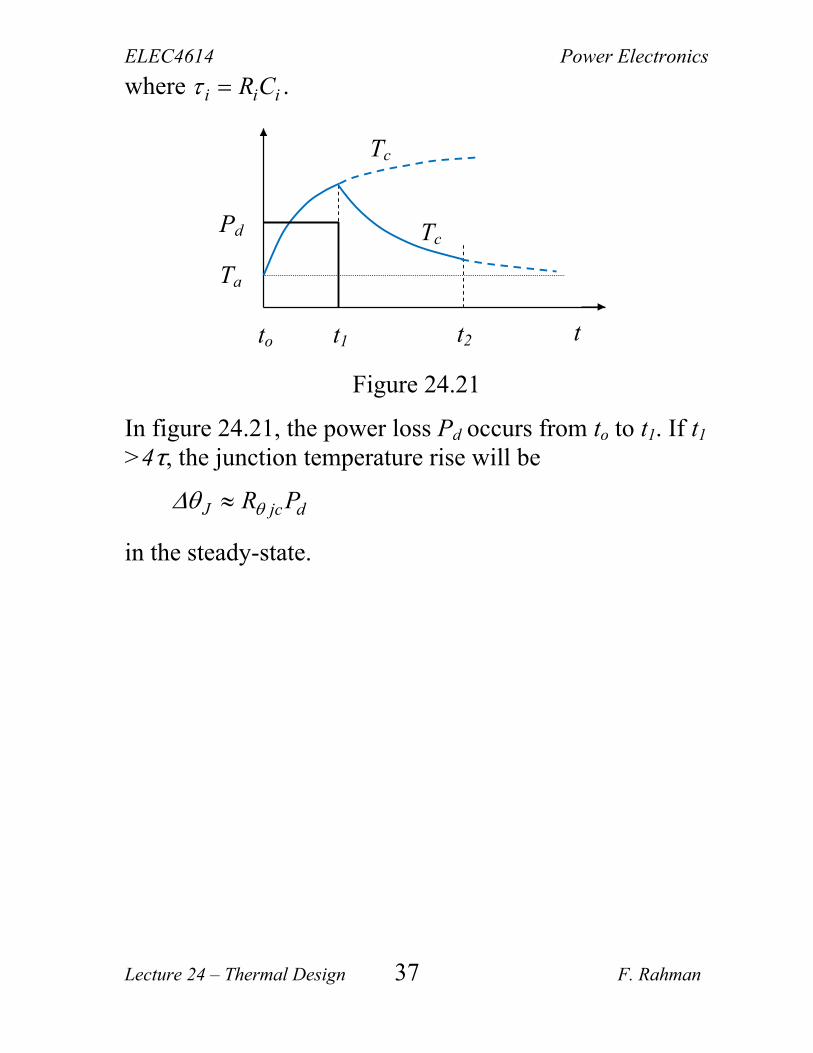
Figure 24.21
In figure 24.21, the power loss Pd occurs from to to t1. If t1 >4τ, the junction temperature rise will be
J jc dR P
in the steady-state.
t2t1 to
Pd
Tc
Ta
Tc
t