electrochemical imaging for microfluidics: a full-system
TRANSCRIPT

1
Supporting Information: Electrochemical imaging for microfluidics: a full-system approach Adnane Karaab, Arnaud Reitzac, Jessy Mathaultb, Syllia Mehou-Lokob, Mehran Abbaszadeh Amirdehi,a Amine Miledb and Jesse Greenera*
1- PCB design and electrode plating:
Custom PCBs were designed in-house and fabricated commercially. A four-layer design was used to give higher electrode density because leads could be stacked over each other at different levels. Vias were covered and insulated in order to handle electrode connections and cross-section routing to avoid liquid leakage and to prevent electrical signal interference as they were submerged in the solution with electrode (Fig. S1).
Figure S1: A schematic showing connections of four electrodes and their internal/external metal leads (gold) in a four layer PCB (green). An insulation layer is also shown (grey). Composite electrode materials, connector assembly and complex routing geometries of internal leads for the entire 200
MEA are not shown. Schematic is not to scale.
The gold layer as received from the manufacturer was prone to failure after a few CV cycles. We attributed this to the thickness of the plating layer of just 10s of nm. Electrode failure was marked by non-reproducible CV curves and a change in colour of the electrode surface, likely due to oxidation and partial erosion of the thin gold layer. Figure S2a and S2b show microscope images of the electrode surface before and after, respectively. The dark spots in the Fig. S2b were attributed to corrosion (with the exception of the electrode edges shown in the top two images).
(a) (b)
Electronic Supplementary Material (ESI) for Lab on a Chip.This journal is © The Royal Society of Chemistry 2016

2
Figure S2. (a) Representative microscope image of the as received electrode surface before CV measurements. (b) Micrographs from 4 different locations on a single as-received electrode after CV measurements. Scale bar in (a) is 20 µm and is representative for all images in (b).
To make the electrodes more robust and longer-lasting, we reconstituted their surfaces. To begin, the original plated materials were stripped by 1 M HCl and then electroplated with a layer of Ni, followed by a layer of Au (Fig. S3). This was accomplished by the reduction of Ni and Au ions, respectively, using the parameters listed in Table S1. As noted in Table S1, two methods of Au plating were used. In the first, the plating solution listed in (a) was synthesised, whereas for the second (b), a commercial plating solution was used.
As described in the main paper, following electrodeposition, we could conduct CV measurements for up to two months without electrode compromise. In addition, the electrodes were stable as pseudo-reference electrodes with no noticeable drift detected in CV signals during their use. Following the process described in the main paper, the MEA was then integrated into the microchannel, forming the sealing layer of the channel.
Figure S3. (a) A partial cross-section showing preparation of two electrodes on PCB MEA. A PCB support material containing electrical connections (cross-hatched) is covered by protective epoxy (green), except where electrodes protrude. After stripping the copper electrode contact pads (blue) are exposed. (b) After electrodeposition of Ni (orange) followed by an Au layer (red). (c) A thin layer of PDMS (approximately hPDMS=50 µm) is patterned around the MEA (red cross-hatch) by spin coating, with the electrodes remaining bare thanks to a removable adhesive barrier that was removed after the process. (d) A PDMS channel (red cross-hatch) with height hchan=50 µm is adhered to the PDMS base-layer by plasma activation. The total channel height after bonding was hPDMS + hchan=100 µm. (e) The footprint of the MECI device showing the MEA placed within the microchannel used here. The cross-section and down-stream dimensions of the overall MEA footprint are MEAx=5.2 mm and MEAy=10.2 mm, respectively. (f) The completed microfluidic device with integrated PCB MEA and connectors. A white outline was added to (f) to highlight the channel walls.
(a)
(b)
(c)
(d)
(e)
(f)MEAy
MEAx
3
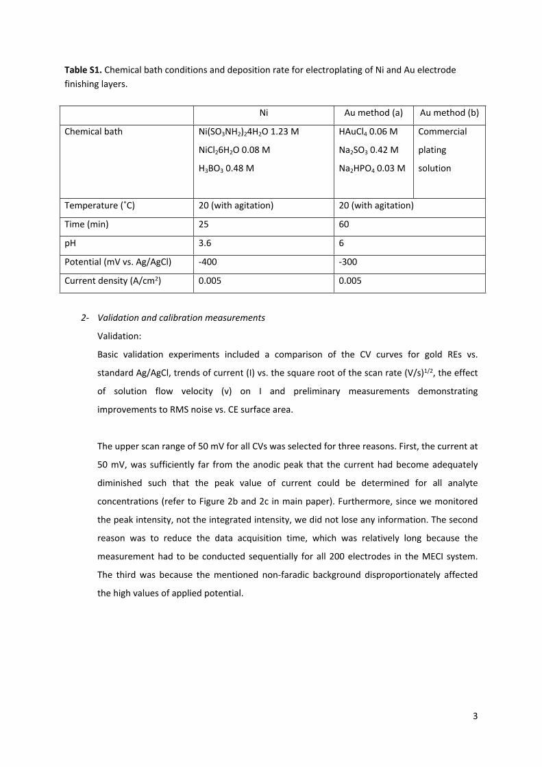
Table S1. Chemical bath conditions and deposition rate for electroplating of Ni and Au electrode finishing layers.
2- Validation and calibration measurements
Validation:
Basic validation experiments included a comparison of the CV curves for gold REs vs.
standard Ag/AgCl, trends of current (I) vs. the square root of the scan rate (V/s)1/2, the effect
of solution flow velocity (v) on I and preliminary measurements demonstrating
improvements to RMS noise vs. CE surface area.
The upper scan range of 50 mV for all CVs was selected for three reasons. First, the current at
50 mV, was sufficiently far from the anodic peak that the current had become adequately
diminished such that the peak value of current could be determined for all analyte
concentrations (refer to Figure 2b and 2c in main paper). Furthermore, since we monitored
the peak intensity, not the integrated intensity, we did not lose any information. The second
reason was to reduce the data acquisition time, which was relatively long because the
measurement had to be conducted sequentially for all 200 electrodes in the MECI system.
The third was because the mentioned non-faradic background disproportionately affected
the high values of applied potential.
Ni Au method (a) Au method (b)
Chemical bath Ni(SO3NH2)24H2O 1.23 M
NiCl26H2O 0.08 M
H3BO3 0.48 M
HAuCl4 0.06 M
Na2SO3 0.42 M
Na2HPO4 0.03 M
Commercial
plating
solution
Temperature (˚C) 20 (with agitation) 20 (with agitation)
Time (min) 25 60
pH 3.6 6
Potential (mV vs. Ag/AgCl) -400 -300
Current density (A/cm2) 0.005 0.005

4
Figure S4. (a) Raw CV curves collected from a single gold WE using Ag/AgCl (dashed) and gold
(solid) acquired in a 10 mM Fe(CN)63−solution at 100 mV·s-1. (b) Anodic current vs. square
root of scan rate and linear fit for a static 6 mM Fe(CN)63− solution confined in the MECI
device. (c) Anodic current of a 10 mM Fe(CN)63− solution (100 mV·s-1) vs. velocity. (d) Signal to
noise with changes to overall CE surface area. Areas were calculated from the use of 1, 3, 5,
10 and 20 CEs in total. Points corresponded to the Fe(CN)63−/4− solutions were 0.8 mM ()
and 10 mM () concentrations.
Applicability of gold pseudo REs and ohmic drop
We demonstrated that any choice of electrode in the MEA as the RE gave similar positions of the
collected CVs. Figure S5A shows CVs collected from Fe(CN)63− solution (100 mV·s-1) using a single
WE and CE combination and 7 different REs at different points in the MEA (Fig. S5b). The average
cathodic and anodic peak positions were -110 mV +/-3.5 mV and -11 mV +/- 5 mV, respectively.
While these values are within the drift error of the measurement, a measurement of the solution
conductivity of 20.4 mS/cm (Orion star A215, Thermo Scientific, USA) suggests that ohmic drop
may not be negligible for certain measurements where CV peaks are closely separated. For the
work in this paper, small shifts of a few mV did not affect our ability to identify the peaks and we
could freely choose any electrode as a RE and get CV curves with comparable peak positions.
Lastly, we noted that the CV curve positions were stable for long durations in between
experiments. Figure S5c shows 5 different CV curves of a Fe(CN)63− solution collected over a more
than 4 month period.
R2=0.974
(a) (b)
(c) (d)

5
Figure S5. (a) Raw CV curves (before
background subtraction) from the
same 8 mM Fe(CN)63− solution (100
mV·s-1). Choice of REs, WE and CEs
are shown in (b). (c) CV curves from
[Fe(CN)6]3− solutions at different
dates (REs and WEs randomly
selected). Solution concentrations
varied.
123
45
61
7
(a) (b)
(c)
-0.5 -0.4 -0.3 -0.2 -0.1 0 0.1 0.2-15
-10
-5
0
5
10
15
20
25
14-août 05-août 04-juil 16-juin05-mai
Potential (V Vs Au)
Cur
rent
(µA
)

6
Calibration curves for MEAs
The range of calibration slopes is the result of electrode-to-electrode variation, likely in their nano-structure. These results demonstrate the need for individual calibration curves for each electrode.
0 0.6 1.2 1.8 2.4 3 3.60
20
40
60
80
100
Calibration slope (µA/mM)
Rel
ativ
e fr
eque
ncy
Figure S6. Histogram of calibration slopes for reconstituted PCB electrodes. Inset shows nano-
structuring. Calibration slope is the same as f(xiyj) in eqn (2) of the main paper.
3- Image processing
Electrochemical imagesWe transformed the raw images into smoothed images to account for concentration gradients between measurement points (Fig. S7a to S7b). This was accomplished first by constructing pixels in the raw images from using a 3x3 matrix of sub pixels, each of the same value. For example in Fig. S6c, we see the value of a pixel with value “a” constructed from 9 sub-pixels. Surrounding the composite pixel, are 8 other composite pixels, with their closest subpixels visible in Fig S7c. Next we implemented a mean smoothing algorithm over all sub-pixels that averaged the nearest neighbours. Fig S6d shows the new value of the original pixel after applying the mean filter, with values of neighbouring sub-pixels excluded for simplicity.
Figure S7. A MEC image (a) before and (b) after implementation of a mean smoothing filter algorithm. The sub-pixel values of a pixel (grey) before (c) and after (d) application of the mean
(a) (b)
(c) (d)

7
smoothing filter algorithm. Colour bar in (a) correlates colour to concentrations for (a) and (b), ranging from 0 mM (blue) to 10 mM (red). Scale bar in (a) is 1 mm.
Graphic user interfaceA graphic user interface (GUI) was developed using Matlab to help the user accurately and easily handle the repetitive treatment of large amounts of data as described in the main paper. The screen capture of the GUI in Figure S8a shows example data as well as the processing options. Options defined parameters related to data import/export, definition of peak intervals, normalization/calibration by background and baseline subtractions, smoothing and display of selected CV curves at different stages of the data treatment process, including a final MEC image. Figure S8b shows an image that was generated by the software, superimposed on the microchannel geometry.
Figure S8. (a) Example screen display from the MECI data analysis software showing screen displays of user selected CV curves at different stages of data treatment as well resulting preliminary image from each WE and all options for data treatment display and file management. (b) Image output after smoothing superimposed on an outline of the microchannels used in this study.
Optical imagingGreyscale optical images of coloured liquid flow streams were acquired using a tripod-mounted digital camera. The freeware ImageJ was used for image treatments, which included (i) a background subtraction using an image obtained from the same region of interest, but containing no coloured flow stream, (ii) application of the “despeckle” filter to remove noise, (iii) false colouring using the “physics” look up table and (iv) adjustment of pixel brightness and contrast to match the image quality to match those produced by simulation software.
4- Simulations
We modeled the change in the interface position between a redox and non-redox stream using Comsol (see experimental section in the main paper for more details) and compared it with current resulting from partial coverage of the electrode in Fig. 6b using equation 4 (both from the main paper). In the simulation, in response to progressive changes to the flow rate ratio, the interface between the two streams changed its position (Fig. S9 and Fig. S10). The flow rate ratio was defined
(a) (b)

8
as the volumetric flow rate of the redox solution (QR) divided by the the total flow rate QT, where QT = QR +QPBS.
Figure S9. Results of numerical simulations showing the displacement of redox and non-redox streams (red and blue, respectively) and their interface (cyan) under different flow rate ratios (QR/QT) 0.52 (a), 0.56 (b), 0.60 (c), 0.65 (d), 0.68 (e) and 0.75 (f). Where QT = 8 mL·h-1 for all cases. Scale bar in (a) is 2.0 mm. Individual electrodes are shown as grey squares.
Figure S10. Close up of an electrode x6y1 (see black electrode in Figure 6a in main paper) as it is progressively exposed to greater surface coverage of the analyte solution (red) for the flow rate ratios (QR/QT) of: 0.52 (a), 0.56 (b), 0.60 (c), 0.65 (d), 0.68 (e) and 0.75 (f). Where QT = 8 mL·h-1. Blue and cyan colours have the same meaning as in Figure S9. The orange squares shows the 340 µm x 340 µm electrode position.
(a) (b) (c) (d) (e) (f)