emc test specification for broadr-reach® transceivers · this emc measurement specification is...
TRANSCRIPT

EMC Test Specification for BroadR-Reach®
Transceivers Version 2.0
Author & Company Dr. Bernd Körber, FTZ Zwickau
Title EMC Measurement Specification for BroadR-Reach® Transceivers
Version 2.0
Date December 19, 2014
Status Final version
Restriction Level Public
This EMC measurement specification shall be used as a standardized common scale for EMC evaluation of Ethernet transceivers for 100 Mbit/s BroadR-Reach® in automotive applications.

OPEN Alliance
Restriction Level: Public | EMC Test Specification for BroadR-Reach® Transceivers | Dec-14 2
Version Control of Document
Version Author Description Date
0.1 B. Körber Initial version 10/23/12
0.2 B. Körber 2cd draft version, discussed changes from telco OA TC1 changed to new OA document template
6/26/13
1.0 B. Körber Editorial changes in diagrams in section C 9/24/13
1.1 B. Körber Disclaimer added 10/04/13
1.2 B. Körber Editorial changes, Pulse modulation added for RF immunity tests Section powered ESD added
09/13/14
1.3 B. Körber Definition for optimized BIN changed 10/02/14
2.0 B. Körber Numbering of version changed 12/19/14
Restriction level history of Document
Version Restriction Level Description Date
0.1 Open internal only 10/23/12
0.2 Open internal only 6/26/13
1.0 Open internal only 9/24/13
1.1 Open internal only 10/04/13
1.2 Public 09/13/14
1.3 Public 10/02/14
2.0 Public 12/19/14
OPEN Alliance
Restriction Level: Public | EMC Test Specification for BroadR-Reach® Transceivers | Dec-14 3
Disclaimer
The OPEN Specifications (including any part thereof) are intended to be used as an information source to
enable to manufacture and test products which comply with the OPEN Specification.
All OPEN Specifications are provided on “as is” basis and all warranties, either explicit or implied, are
excluded unless mandatory under law. Accordingly, the OPEN Alliance Members who have contributed to
the OPEN Specifications make no representations or warranties with regard to the OPEN Specifications or
the information (including any software) contained therein, including any warranties of merchantability,
fitness for purpose, or absence of third party rights and make no representations as to the accuracy or
completeness of the OPEN Specifications or any information contained therein.
The OPEN Alliance Members who have contributed to the OPEN Specifications will not be liable for any
losses, costs, expenses or damages arising in any way out of use or reliance upon any OPEN Specification
or any information therein. Nothing in this document operates to limit or exclude any liability for fraud or
any other liability which is not permitted to be excluded or limited by operation of law.
The material contained in OPEN Specifications is protected by copyright and may be subject to other types
of Intellectual Property Rights. OPEN Specifications (or any part thereof) shall be distributed only among
those bound by the confidentiality defined for the OPEN Specification and as announced in the OPEN
Specification documents.
The distribution of OPEN Specifications shall not operate as an assignment or license to any recipient of
any OPEN Specification of any patents, registered designs, unregistered designs, trademarks, trade names
or other rights as may subsist in or be contained in or reproduced in any OPEN Specification. The
commercial exploitation of the material in this document may require such a license, and any and all
liability arising out of use without such a license is excluded.
OPEN Specification documents may be reproduced in electronic or paper form or utilized in order to
achieve the Scope only. Reproduction or utilization for any other purposes as well as any modification of
the Specification document, in any form or by any means, electronic or mechanical, including
photocopying and microfilm, is explicitly excluded.
Without prejudice to the foregoing, the OPEN Alliance Specifications have been developed for automotive
applications only. They have neither been developed, nor tested for non-automotive applications.
OPEN Alliance reserves the right to withdraw, modify, or replace any OPEN Specification at any time,
without notice.

OPEN Alliance
Restriction Level: Public | EMC Test Specification for BroadR-Reach® Transceivers | Dec-14 4
Contents 1 Introduction .......................................................................................................................................... 5
1.1 Scope ............................................................................................................................................. 5
1.2 References .................................................................................................................................... 5
1.3 List of abbreviations and definitions ............................................................................................. 6
2 Test Philosophy ..................................................................................................................................... 7
2.1 General .......................................................................................................................................... 7
2.2 Tested EMC phenomena ............................................................................................................... 8
3 Required Tests ...................................................................................................................................... 9
3.1 RF and transient disturbances ...................................................................................................... 9
3.1.1 General test conditions for RF and transient disturbances .................................................. 9
3.1.2 Emission of RF disturbances................................................................................................ 16
3.1.3 Immunity to RF disturbances .............................................................................................. 20
3.1.4 Immunity to transients ....................................................................................................... 25
3.2 ESD .............................................................................................................................................. 30
3.2.1 Unpowered ESD test ........................................................................................................... 30
3.2.2 Powered ESD test ................................................................................................................ 35
Appendix A - Test circuit boards ................................................................................................................. 38
A.1 RF and transient tests ................................................................................................................. 38
A.2 ESD tests ...................................................................................................................................... 40
Appendix B - Required information from semiconductor manufacturer ................................................... 41
Appendix C – Recommended limits for tests .............................................................................................. 42
C.1 Emission of RF disturbances ....................................................................................................... 42
C.2 Immunity to RF disturbances ...................................................................................................... 43
C.3 Immunity to transients ............................................................................................................... 44
C.4 ESD .............................................................................................................................................. 44

OPEN Alliance
Restriction Level: Public | EMC Test Specification for BroadR-Reach® Transceivers | Dec-14 5
1 Introduction
1.1 Scope
This EMC measurement specification shall be used as a standardized common scale for EMC evaluation
of Ethernet transceivers for 100 Mbit/s BroadR-Reach® in automotive applications according to [OPEN1].
It contains recommended limits. The final judgment of the tested device is left to the customer.
This specification is not applicable for devices which are intended for use in Power over Ethernet
applications.
This specification uses standard EMC test methods for ICs according to [IEC1,2], [IEC3,4] and [IEC5] and
can be applied for stand-alone transceivers and integrated transceiver cells. In case of devices with an
integrated Ethernet transceiver (e.g. SBCs), the test conditions cannot be fixed for each type of IC.
Therefore, if it is possible, the test conditions of standard stand-alone transceiver should be used. The
configuration of the physical layer of the Ethernet communication system is fixed in any case.
All EMC relevant pins (functions) described in this document shall be tested. If an Ethernet transceiver
includes additional product specific EMC relevant pins (functions) it shall be tested as well. The test
conditions and failure validation criteria shall be adapted to the definitions for stand-alone Ethernet
transceiver.
1.2 References
[OPEN1] Broadcom / OPEN Alliance BroadR-Reach® (OABR) Physical Layer Transceiver Specification For Automotive Applications, Version 3.2
[IEC1] IEC 61967-1, Integrated circuits, Measurement of electromagnetic emissions, 150 kHz to 1 GHz – Part 1: General and definitions
[IEC2] IEC 61967-4, Integrated circuits, Measurement of electromagnetic emissions, 150 kHz to 1 GHz – Part 4: Measurement of conducted emissions – 1 Ω/150 Ω direct coupling method
[IEC3] IEC 62132-1, Integrated circuits, Measurement of electromagnetic immunity, 150 kHz to 1 GHz – Part 1: General and definitions
[IEC4] IEC 62132-4, Integrated circuits, Measurement of electromagnetic immunity, 150 kHz to 1 GHz – Part 4: Direct RF power injection method
[IEC5] IEC62215-3: Integrated circuits – Measurement of impulse immunity: Part 3: Non-synchronous transient injection method … (Actually unpublished draft version)
[IEC6] IEC 61000-4-2, Electromagnetic compatibility, Part 4-2: Testing and measurement techniques – Electrostatic discharge immunity test

OPEN Alliance
Restriction Level: Public | EMC Test Specification for BroadR-Reach® Transceivers | Dec-14 6
[ISO1] ISO 7637-2, Road vehicles, electrical disturbances by conduction and coupling – Part 2: Vehicles with nominal 12 V or 24 V supply voltage – Electrical transients along supply lines only
[ISO2] ISO 7637-3, Road vehicles, electrical disturbances by conduction and coupling – Part 3: Vehicles with nominal 12 V or 24 V – Electrical transmission by capacitive and inductive coupling via lines other than supply lines
1.3 List of abbreviations and definitions
AM: Amplitude Modulation
BIN: MDI Test Network
CMC: Common Mode Choke
CW: Continuous Wave
DPI: Direct Power Injection
DTT: Data Transfer Test
Global pin: Pins that can be connected direct or via external passive components to the wiring
harness
LPF: Low Pass Filter
MDI: Medium Dependent Interface
MII: Media Independent Interface
PM: Pulse Modulation
RF: Radio Frequency
SBC: System Basis Chip

OPEN Alliance
Restriction Level: Public | EMC Test Specification for BroadR-Reach® Transceivers | Dec-14 7
2 Test Philosophy
2.1 General
Due to the high communication rate of BroadR-Reach® Ethernet and the intended use of unshielded
twisted pair cable for automotive applications, a high risk of EMC problems is expected. For this reason,
an EMC optimization of all components of the Ethernet physical layer is required. The EMC results are
influenced by different aspects:
Ethernet transceiver software configuration (register settings)
Ethernet transceiver itself
MDI test network (BIN)
layout implementation of transceiver and interface network
other active ICs that are necessary for Ethernet communication and for function of application
device (e.g. µC)
EMC concept of application device
symmetry of Ethernet wire and connector
disturbing transfer function of used test and measuring method.
An advantageous strategy for EMC optimization of the application device is to analyze the influence of
each aspect separately.
This EMC measurement specification is focused on the physical layer of the Ethernet interface using
standard EMC test methods for ICs. The intent of this specification is:
a common EMC evaluation of BroadR-Reach® transceiver for comparison purpose
checking the EMC behavior of the transceiver in combination with different MDI test networks
separation of emitted disturbance into disturbing source:
MDI pins
voltage supplies
other digital interfaces (e.g. MII)
evaluation of EMC behavior for symmetrical and unbalanced disturbances at MDI pins

OPEN Alliance
Restriction Level: Public | EMC Test Specification for BroadR-Reach® Transceivers | Dec-14 8
2.2 Tested EMC phenomena
Derived from the EMC requirements at the application layer, tests for the following EMC phenomena are
specified:
EMC phenomena Transceiver pins Test method
RF emission
MDI
voltage supply pins
other global pins
(e.g. VBAT pin)
150 Ohm test method acc. to [IEC2]
RF immunity MDI
other global pins DPI test method acc. to [IEC4]
Transient immunity MDI
other global pins [ISO1] pulses using [IEC5]
ESD immunity MDI
other global pins discharge module according to [IEC6]
Table 2-1: Tested EMC phenomena and related test methods

OPEN Alliance
Restriction Level: Public | EMC Test Specification for BroadR-Reach® Transceivers | Dec-14 9
3 Required Tests
3.1 RF and transient disturbances
3.1.1 General test conditions for RF and transient disturbances
3.1.1.1 Test conditions
The general test conditions are given below.
Parameter Value
Battery voltage supply (14.0 0.2) V
Voltage supply, auxiliary supply (Unom 0.1) V
Test ambient temperature (23 5) C
Table 3-1: General test conditions
3.1.1.2 Test configuration
For testing the EMC behavior (except ESD) of Ethernet transceivers the following node to node network
is used.
CN
Node 2
MDI
Proper function / error indication Node 1
µC
TC µC BIN MII interface
MDI P
TC BIN MII interface
CN
CN Supplies / others
Supplies / others
VX
VXX
Proper function / error indication
Proper function /
error indication Proper function / error indication
MDI N
MDI P
CN
Other global
pins (X) MDI N
X
µC Automotive microcontroller with MII interface
TC Ethernet transceiver (device under test – DUT)
BIN MDI test network (including DC decoupling, CMC and if used: termination, additional filter elements and ESD protection devices)
CN EMC coupling network
Figure 3-1: Basic test configuration for RF and transient tests at Ethernet transceiver

OPEN Alliance
Restriction Level: Public | EMC Test Specification for BroadR-Reach® Transceivers | Dec-14 10
An Ethernet node consists of a microcontroller, the Ethernet transceiver and a MDI test network. Both
nodes are equivalently configured to establish a full duplex Ethernet link. The link has one bidirectional
connection. This connection is carried out as line impedance controlled PCB traces and not a wire
connection.
The microcontroller (e.g. Freescale MPC5567) used for this setup implements an MII interface which is
used for configuring and monitoring the Ethernet transceiver and for generating an Ethernet test signal.
If an MII interface is not available on the Ethernet transceiver, another interface (such as MDIO or SPI)
should be used. The µC is EMC decoupled from the tested transceiver (and its EMC coupling networks)
using filter networks at voltage supplies and by considering specific layout requirements. A specific
software implementation runs on the µC. It must be adapted to the transceiver type, especially for
configuration and monitoring.
If a multiport device is being evaluated, each port that is intended to be used for wired Ethernet
communication must be tested. Doing this, the tested port of node 1 shall be connected with the same
port of node 2 (port1 with port 1, port 2 with port 2, …).
The Ethernet transceiver (TC) has a circuitry of external passive components according to the data sheet
requirements of the semiconductor manufacturer.
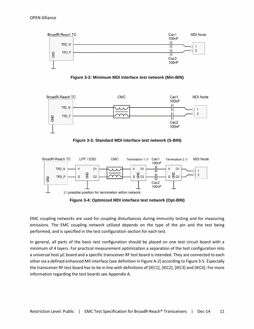
Three different types of MDI test networks (BIN) shall be used for testing:
Minimum MDI interface network (Min-BIN):
DC decoupling capacitor Cac1 = Cac2 = 100 nF )1 and a biasing network (if required for operation)
as illustrated in Figure 3-2
Standard MDI interface (S-BIN):
DC decoupling capacitor Cac1 = Cac2 = 100 nF )1, a biasing network (if required for operation) and
a CMC that fulfill the requirements of [OPEN 2] Appendix B.1 as illustrated in Figure 3-3
Optimized MDI interface (Opt-BIN):
DC decoupling capacitor Cac1 = Cac2 = 100 nF )1, a biasing network (if required for operation), a
CMC that fulfill the requirements of [OPEN 2] Appendix B.1 and a Low pass filter (LPF), ESD
suppression devices or terminations defined by semiconductor manufacturer as illustrated in
Figure 3-4. The position of the termination within the interface network can diversity between
CMC and Cac1/ Cac2 or between Cac1 and Cac2 and MDI node.
)1 Cac1 = Cac2 = 100 nF is default value. Other values can be used if required by semiconductor manufacturer.
The S- Parameters SCC21, SDD21, SDC21 and SCD21 of CMC samples used during testing shall be measured according to [OPEN 2] and shall be documented in the test report.
OPEN Alliance
Restriction Level: Public | EMC Test Specification for BroadR-Reach® Transceivers | Dec-14 11
Figure 3-2: Minimum MDI interface test network (Min-BIN)
Figure 3-3: Standard MDI interface test network (S-BIN)
Figure 3-4: Optimized MDI interface test network (Opt-BIN)
EMC coupling networks are used for coupling disturbances during immunity testing and for measuring
emissions. The EMC coupling network utilized depends on the type of the pin and the test being
performed, and is specified in the test configuration section for each test.
In general, all parts of the basic test configuration should be placed on one test circuit board with a
minimum of 4 layers. For practical measurement optimization a separation of the test configuration into
a universal host µC board and a specific transceiver RF test board is intended. They are connected to each
other via a defined enhanced MII interface (see definition in Figure A-2) according to Figure 3-5. Especially
the transceiver RF test board has to be in line with definitions of [IEC1], [IEC2], [IEC3] and [IEC4]. For more
information regarding the test boards see Appendix A.

OPEN Alliance
Restriction Level: Public | EMC Test Specification for BroadR-Reach® Transceivers | Dec-14 12
CN
Node 2
µC
TC µC BIN
Enhanced MII interfaces
TC BIN
CN
CN Node 1
Host µC board Transceiver RF board
MII interface
MII interface
Voltage supply
Voltage supply
Figure 3-5: Arrangement of host µC board and transceiver RF test board

OPEN Alliance
Restriction Level: Public | EMC Test Specification for BroadR-Reach® Transceivers | Dec-14 13
3.1.1.3 Definitions for Ethernet test communication and software configuration of transceiver
The Ethernet test communication signals for 100 Mbit/s communication rate in full duplex mode are
defined as:
Topic Content
Software
MDI relevant configuration for tests in active mode (normal mode):
BroadR-Reach® full duplex
Automatic Polarity Detection enabled (if implemented)
Driver strength maximum - default (if configurable)
Transceiver configuration specified by semiconductor manufacturer (to be
documented in the test report)
Data frame transmission with 10 ms cycle time
Data frame format:
Protocol type TCP/IP 0x800
Data length 58 byte
Data 0xAA
MDI relevant configuration for tests in low power mode (sleep or standby mode):
Transceiver configuration as specified by semiconductor manufacturer (to be
documented at test report)
MII relevant configuration:
Transceiver configuration as specified by semiconductor manufacturer (e.g. MII
driver strength, to be documented at test report)
Table 3-2: Definition for software configuration
For additional tests, especially in combination with optimized BIN, other configurations for reduction of
emission or improvement of immunity can be used. For all combinations tested, Ethernet communication
must be possible over 15 m of UTP cable and 4 standard inline connectors in the absence of disturbers.
The transceiver configuration data necessary for standard and, if used, for EMC optimized configuration
must be supplied by the semiconductor manufacturer. It must be documented in detail (register write
data and order of writing) in the test report.

OPEN Alliance
Restriction Level: Public | EMC Test Specification for BroadR-Reach® Transceivers | Dec-14 14
3.1.1.4 Evaluation of system immunity
A malfunction test and a damage test are required to evaluate system immunity. The malfunction test
examines function status class A while the damage test examines function status classes C and D (see
Table 3-3).
3.1.1.4.1 Malfunction test
A malfunction test is required to be performed after a link is established between two test transceivers
(normal mode) or the transceivers are set into low power mode, if available. The following criteria will be
evaluated:
Evaluation during immunity tests for tests in normal mode (I-n)
If possible, read out of all available error registers for the transceiver. At a minimum the
register information for Link error and CRC error should be examined.
Note1: If no read out of required error registers at the transceiver is possible, the error validation
shall be implemented into the microcontroller software in comparable way.
Data Transfer Test (DTT) error detection by microcontroller software application (checking
of all transferred data between the two nodes of the test network)
Evaluation during immunity tests for tests in low power mode (I-lp)
Check indication for wakeup
Evaluation after immunity tests for tests in normal mode (II-n)
Read out of transceiver configuration registers and comparison with initial state
3.1.1.4.2 Damage test
A damage test related to functional status class D means that one or more functions of a transceiver do
not perform as designed during exposure and do not return to normal operation until exposure is removed
and the transceiver is reset by simple "operator/use" action (e.g. restart by MII interface). No physical
damage of transceiver occurs.
The following evaluation criteria have to be used for detection of a physical damage:
Evaluation criterion 1: Evaluation of current consumption at voltage supply input(s) of tested
transceiver after damage test. Any change of more than 5 % of the initial value indicates a
damage of the tested pin.
Evaluation criterion 2: Evaluation of functionality of tested transceiver after damage test and
reset by simple "operator/use", if necessary.
Evaluation criterion 3: The characteristic curve of pin voltage versus pin current of the tested pin
to GND pin must be measured using a Semiconductor Parameter Analyzer. If possible the
maximum current and voltage level used for characteristic curve measurement should be
indicating the break down voltage of the internal ESD structure. Commonly used voltages are
± (50 to 70) V and ± (0.5 to 5) mA. Any change of more than 5 % of the maximum used voltage
or current indicates a damage of the tested pin.

OPEN Alliance
Restriction Level: Public | EMC Test Specification for BroadR-Reach® Transceivers | Dec-14 15
Figure 3-6: Example for maximum deviation definition at characteristic curve measurement
3.1.1.4.3 Resulting status classes
The test results shall be related to function status class A or C using the definitions of Table 4.
Resulting status class Comment
A no error occurred during exposure (I-n / I-lp)
C
error occurred during exposure (I-n)
no error after exposure (A)
no change of internal transceiver configuration (II)
system comes back into proper operation automatically
D
error occurred during exposure (I-n)
error occurred after exposure (I-n) or change of internal
transceiver configuration (II)
system does not come back into proper operation
automatically until exposure is removed and the
transceiver is reset by simple "operator/use" action
(e.g. power off/on)
no physical damage of IC occurs (according to section
3.1.1.4.2)
Table 3-3: Definition for immunity status classes
The failure validation applies to both transceivers of the node to node test network. As soon as at least
one transceiver in the network fulfils the fault criteria, the error event for this test has occurred.

OPEN Alliance
Restriction Level: Public | EMC Test Specification for BroadR-Reach® Transceivers | Dec-14 16
3.1.2 Emission of RF disturbances
3.1.2.1 Test configuration
For measuring RF emissions the basic test configuration given in Figure 3-1 is used. The EMC coupling
networks are defined for the 150 Ohm RF voltage measurement at the MDI, voltage supply pins and other
global pins.
For each Ethernet link a symmetrical measuring network given in Figure 3-7 is used. The difference
between symmetrical passive components C1 and C2 as well as R1 and R2 must be less than or equal to
0.1 %, which can be confirmed by measurement.
EMI1
RF Analyzer Test board
Ri 50
Rm1 51
120
MDI P
MDI N
470 pF
C1
C2
R1
R2
120 470 pF
Comment: The resistors R1(2) (120 ) in series with [Rm1 (51 ) parallel to Ri (50 )] and in
combination with capacitors C1(2) represent the 150 Ohm RF voltage measurement network.
Figure 3-7: RF emission measuring network for Ethernet link
The emission at each voltage supply pin of the transceiver, which is connected to the application device
voltage supply, must be measured using the network given in Figure 3-8. The central voltage Vx (Vx
represents different possible voltage supply domains) is RF decoupled from the transceiver pin with an
inductor Lx = 4.7 µH. The decoupling capacitor Cdec or multi-stage filter – according to data sheet
definitions – is placed directly at the transceiver pin.
EMIx
RF Analyzer Test board
120
pin Vx Rx
Ri 50
Rmx 51
6.8 nF
Cx
Cdec
4.7 µH
Vx
Lx
Comment: The resistor Rx (120 ) in series with [Rmx (51 ) parallel to Ri (50 )] and in
combination with capacitor Cx represent the 150 Ohm RF voltage measurement network.
Figure 3-8: RF emission measuring network for voltage supply pins
OPEN Alliance
Restriction Level: Public | EMC Test Specification for BroadR-Reach® Transceivers | Dec-14 17
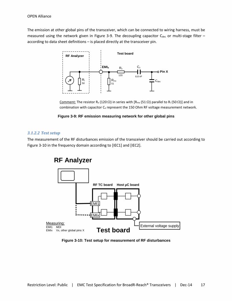
The emission at other global pins of the transceiver, which can be connected to wiring harness, must be
measured using the network given in Figure 3-9. The decoupling capacitor Cdec or multi-stage filter –
according to data sheet definitions – is placed directly at the transceiver pin.
EMIX
RF Analyzer Test board
120
Pin X Rx
Ri 50
Rmx 51
6.8 nF
Cx
Cdec
Comment: The resistor Rx (120 ) in series with [Rmx (51 ) parallel to Ri (50 )] and in
combination with capacitor Cx represent the 150 Ohm RF voltage measurement network.
Figure 3-9: RF emission measuring network for other global pins
3.1.2.2 Test setup
The measurement of the RF disturbances emission of the transceiver should be carried out according to
Figure 3-10 in the frequency domain according to [IEC1] and [IEC2].
RF Analyzer
Test board External voltage supply
Measuring: EMI1 MDI EMIx Vx, other global pins X
EMI1
EMIx
Host µC board RF TC board
Figure 3-10: Test setup for measurement of RF disturbances

OPEN Alliance
Restriction Level: Public | EMC Test Specification for BroadR-Reach® Transceivers | Dec-14 18
Test equipment requirements:
RF Analyzer: Spectrum analyzer or measuring receiver according to [IEC1]
Test board: according to Appendix A
External voltage supply
The insertion losses (S21 measurement) of the respective transceiver signal pad to the ports EMI1 through
EMIx of the test board (without transceiver) shall be measured and documented in the test report.
3.1.2.3 Test procedure and parameters
For characterization of the emission the following test parameters listed in Table 3-4 shall be applied. The
results shall be presented as a diagram in the test report.
Mode Coupling
Port Pin MDI test network (BIN)
Parameter coupling
normal mode /
with Ethernet
test
communication
EMI1 MDI
P / N
minimum symmetric
standard
symmetric
+/- 2.5 % unbalance )1
+/- 5.0 % unbalance )1
optimized
Symmetric
+/- 2.5 % unbalance )1
+/- 5.0 % unbalance )1
EMIx voltage
supplies Vx
standard or
optimized simple one-stage filter at Vx
standard or
optimized
optimized filter or supplier
specific filter at Vx
EMIx other global
pins
standard or
optimized
pin circuit according to data
sheet or application hints
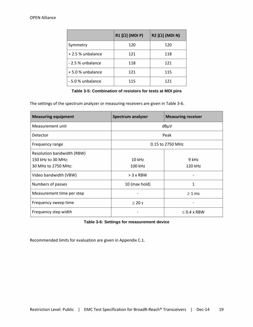
)1 To adjust the unbalance of coupling, the resistance values of the two coupling resistors R1 and R2 shall be changed according to Table 3-5.
Table 3-4: Required emission measurements
OPEN Alliance
Restriction Level: Public | EMC Test Specification for BroadR-Reach® Transceivers | Dec-14 19
R1 [] (MDI P) R2 [] (MDI N)
Symmetry 120 120
+ 2.5 % unbalance 121 118
- 2.5 % unbalance 118 121
+ 5.0 % unbalance 121 115
- 5.0 % unbalance 115 121
Table 3-5: Combination of resistors for tests at MDI pins
The settings of the spectrum analyzer or measuring receivers are given in Table 3-6.
Measuring equipment Spectrum analyzer Measuring receiver
Measurement unit dBµV
Detector Peak
Frequency range 0.15 to 2750 MHz
Resolution bandwidth (RBW)
150 kHz to 30 MHz:
30 MHz to 2750 MHz:
10 kHz
100 kHz
9 kHz
120 kHz
Video bandwidth (VBW) > 3 x RBW -
Numbers of passes 10 (max hold) 1
Measurement time per step - 1 ms
Frequency sweep time 20 s -
Frequency step width - 0.4 x RBW
Table 3-6: Settings for measurement device
Recommended limits for evaluation are given in Appendix C.1.
OPEN Alliance
Restriction Level: Public | EMC Test Specification for BroadR-Reach® Transceivers | Dec-14 20
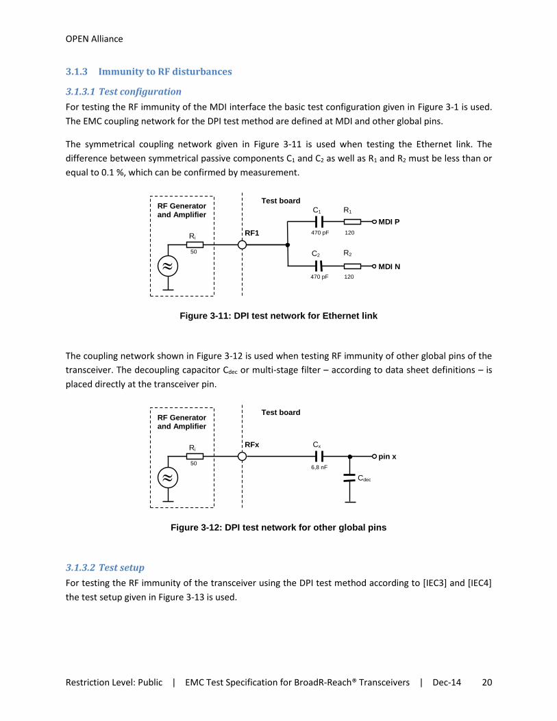
3.1.3 Immunity to RF disturbances
3.1.3.1 Test configuration
For testing the RF immunity of the MDI interface the basic test configuration given in Figure 3-1 is used.
The EMC coupling network for the DPI test method are defined at MDI and other global pins.
The symmetrical coupling network given in Figure 3-11 is used when testing the Ethernet link. The
difference between symmetrical passive components C1 and C2 as well as R1 and R2 must be less than or
equal to 0.1 %, which can be confirmed by measurement.
RF1
RF Generator and Amplifier
Test board
Ri
50
120
MDI P
MDI N
470 pF
C1
C2
R1
R2
120 470 pF
Figure 3-11: DPI test network for Ethernet link
The coupling network shown in Figure 3-12 is used when testing RF immunity of other global pins of the
transceiver. The decoupling capacitor Cdec or multi-stage filter – according to data sheet definitions – is
placed directly at the transceiver pin.
RFx
RF Generator and Amplifier
Test board
Ri
50 pin x
6,8 nF
Cx
Cdec
Figure 3-12: DPI test network for other global pins
3.1.3.2 Test setup
For testing the RF immunity of the transceiver using the DPI test method according to [IEC3] and [IEC4]
the test setup given in Figure 3-13 is used.

OPEN Alliance
Restriction Level: Public | EMC Test Specification for BroadR-Reach® Transceivers | Dec-14 21
Monitoring
DSO
Test board External voltage supply
RF1
Host µC board RF TC board
RF Generation
Power meter
RF Generator
RF Amplifier
Control PC
RFx
Testing: RF1 MDI RFx other global pins x
Figure 3-13: Test setup for RF immunity testing
Test equipment requirements:
RF Generator: f = 1 – 1000 MHz, modulation AM and PM
RF Amplifier: PCW 10 W
RF Power meter with
directional coupler:
f = 1 - 1000 MHz
Test board: according to Appendix A
DSO
External voltage supply
Control PC
Semiconductor
parameter analyzer: used for I/V measurement after damage test
The insertion losses (S21 measurement) of ports RF1 through RFx to the respective transceiver signal pad
of the test board (without transceiver) shall be measured and documented in the test report.
OPEN Alliance
Restriction Level: Public | EMC Test Specification for BroadR-Reach® Transceivers | Dec-14 22
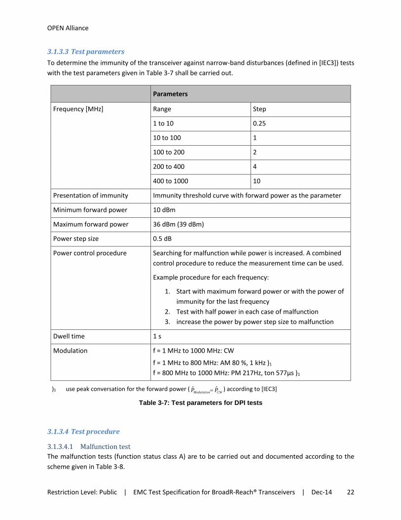
3.1.3.3 Test parameters
To determine the immunity of the transceiver against narrow-band disturbances (defined in [IEC3]) tests
with the test parameters given in Table 3-7 shall be carried out.
Parameters
Frequency [MHz] Range Step
1 to 10 0.25
10 to 100 1
100 to 200 2
200 to 400 4
400 to 1000 10
Presentation of immunity Immunity threshold curve with forward power as the parameter
Minimum forward power 10 dBm
Maximum forward power 36 dBm (39 dBm)
Power step size 0.5 dB
Power control procedure Searching for malfunction while power is increased. A combined
control procedure to reduce the measurement time can be used.
Example procedure for each frequency:
1. Start with maximum forward power or with the power of
immunity for the last frequency
2. Test with half power in each case of malfunction
3. increase the power by power step size to malfunction
Dwell time 1 s
Modulation f = 1 MHz to 1000 MHz: CW
f = 1 MHz to 800 MHz: AM 80 %, 1 kHz )1
f = 800 MHz to 1000 MHz: PM 217Hz, ton 577µs )1
)1 use peak conversation for the forward power (CWModulation PP ˆˆ ) according to [IEC3]
Table 3-7: Test parameters for DPI tests
3.1.3.4 Test procedure
3.1.3.4.1 Malfunction test
The malfunction tests (function status class A) are to be carried out and documented according to the
scheme given in Table 3-8.

OPEN Alliance
Restriction Level: Public | EMC Test Specification for BroadR-Reach® Transceivers | Dec-14 23
Mode Coupling Failure validation class A
Error / Function
Port Pin
MDI test network
(BIN) Parameter coupling CRC Link DTT Sum)4
Wake up
normal mode /
with Ethernet test communi-cation
RF1 MDI P / N
minimum )2 symmetric X
standard )3
symmetric X X X X
+/- 2.5% unbalance )1 X
+/- 5% unbalance )1 X
optimized )3
symmetric X
+/- 2.5% unbalance )1 X
+/- 5% unbalance )1 X
RFx other global pins
standard or optimized)2
pin circuit according to data sheet or application hints
X
low power mode / test of wanted wakeup )5,6
RF1 MDI P / N
minimum )2 symmetric
X
standard )3
symmetric X
+/- 2.5% unbalance )1 X
+/- 5% unbalance )1 X
optimized )3
symmetric X
+/- 2.5% unbalance )1 X
+/- 5% unbalance )1 X
low power mode / test of unwanted wakeup )5
RF1 MDI P / N
minimum )2 symmetric X
standard )3
symmetric X
+/- 2.5% unbalance )1 X
+/- 5% unbalance )1 X
optimized )3
symmetric X
+/- 2.5% unbalance )1 X
+/- 5% unbalance )1 X
)1 To adjust the unbalance of coupling the resistance values of the two coupling resistors R1 and R2 shall be changed according to Table 3-5.
)2 Test shall be done with CW and modulation (AM, PM), maximum test power 36 dBm
)3 Test shall be done only with modulation (AM, PM), maximum test power 39 dBm
)4 Sum error: CRC, Link and DTT evaluated in parallel
)5 Test to wanted or unwanted wake up or Ethernet signal activity detection, depending on implemented function
)6 One node is set to low power mode, second node sends periodically signal to be detected as wakeup by node in low power mode.
Table 3-8: Required DPI tests for malfunction test

OPEN Alliance
Restriction Level: Public | EMC Test Specification for BroadR-Reach® Transceivers | Dec-14 24
For each test an immunity threshold curve with the forward power as the parameter has to be carried out
and has to be presented in the test report in a diagram.
Recommended limits for evaluation are given in Appendix C.2.
3.1.3.4.2 Damage test
The damage tests are to be carried out and documented according to the scheme given in Table 3-9. The
fault criteria are evaluated after each single test. All tests shall be done only with modulation (AM, PM).
Mode Coupling Failure validation class
Port Pin MDI test network (BIN)
Parameter coupling
normal mode
/ with
Ethernet test
communi-
cation
RF1 MDI
P / N
standard or
optimized symmetric
C or D
must be stated as test
result RFx
other
global
pins
standard or
optimized
pin circuit according to
data sheet or application
hints
Table 3-9: Required DPI tests for damage test
Recommended limits are given in Appendix C.2.

OPEN Alliance
Restriction Level: Public | EMC Test Specification for BroadR-Reach® Transceivers | Dec-14 25
3.1.4 Immunity to transients
3.1.4.1 Test configuration
For testing the immunity against transients at the MDI interface the basic test configuration given in Figure
3-1 is used. The EMC coupling networks are defined for the direct capacitive coupling (DCC) defined at
MDI and other global pins.
The symmetrical coupling network given in Figure 3-14 is used when testing the Ethernet link. The
difference between symmetrical passive components C1 and C2 must be less than or equal to 0.1 %, which
can be confirmed by measurement.
IMP1
Transient generator
Test board
Ri
MDI P
MDI N
100 pF
C1
C2
100 pF
Figure 3-14: Transient test network for Ethernet link
The coupling network shown in Figure 3-15 is used when testing transient immunity of other global pins
of the transceiver. The decoupling capacitor Cdec or multi-stage filter – according to data sheet definitions
– is placed directly at the transceiver pin. If coupling to VBAT pin, the coupling capacitor Cx has to be
replaced by a reverse protection diode.
IMPx
Transient generator
Test board
Ri pin x
1 nF
Cx
Cdec
Figure 3-15: Transient test network for other global pins
OPEN Alliance
Restriction Level: Public | EMC Test Specification for BroadR-Reach® Transceivers | Dec-14 26
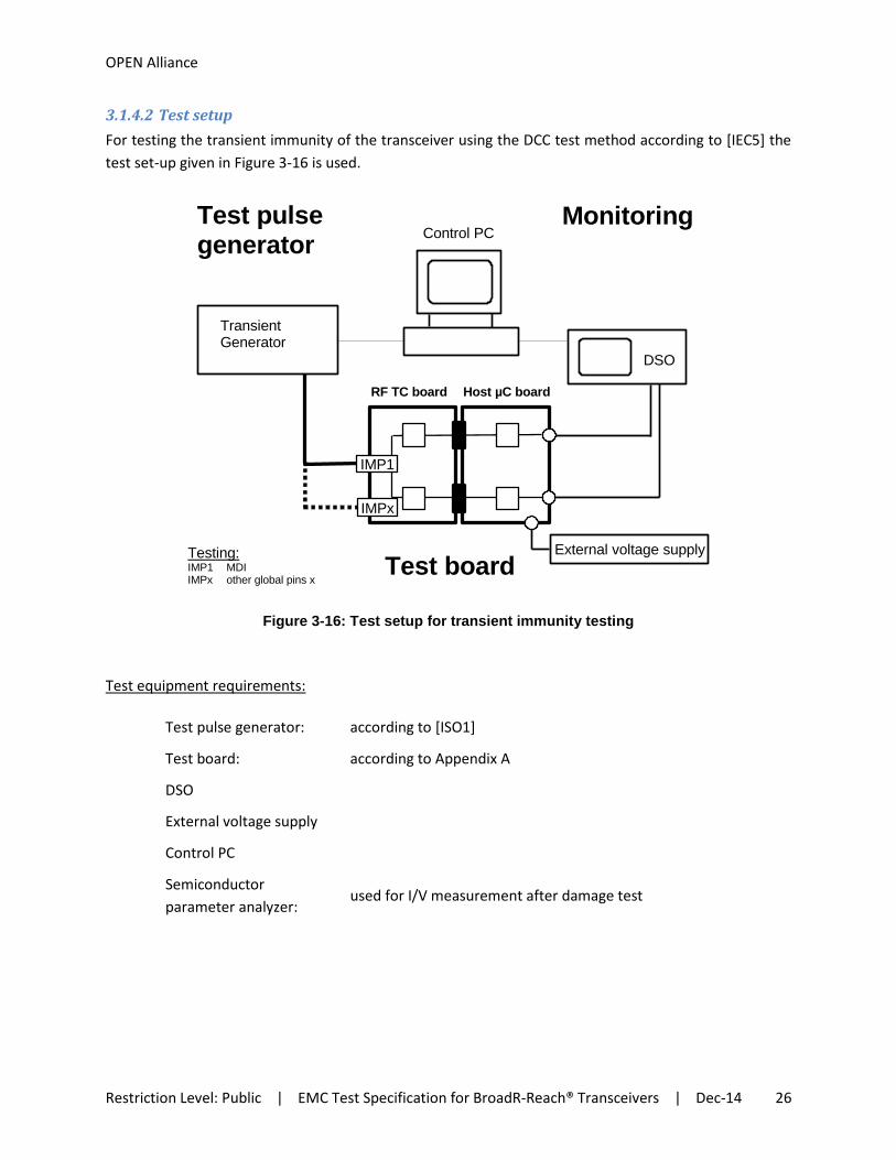
3.1.4.2 Test setup
For testing the transient immunity of the transceiver using the DCC test method according to [IEC5] the
test set-up given in Figure 3-16 is used.
Monitoring
DSO
Test board External voltage supply
IMP1
Host µC board RF TC board
Test pulse generator
Transient Generator
Control PC
IMPx
Testing: IMP1 MDI IMPx other global pins x
Figure 3-16: Test setup for transient immunity testing
Test equipment requirements:
Test pulse generator: according to [ISO1]
Test board: according to Appendix A
DSO
External voltage supply
Control PC
Semiconductor
parameter analyzer: used for I/V measurement after damage test

OPEN Alliance
Restriction Level: Public | EMC Test Specification for BroadR-Reach® Transceivers | Dec-14 27
3.1.4.3 Test parameters
To prove transceiver immunity against transient tests with standard pulses (defined in [ISO1]) tests with
parameters given in Table 12 shall be carried out.
Test pulse )1 Pulse repetition frequency [Hz]
(1/T1 )1)
Test duration )3 [s]
Ri [] Remarks
1)2 2
600 / 60 / 5
10 t2 = 0 s
2a 2 2
3a 10000 50
3b 10000 50
)1 according to [ISO1]
)2 parameters for 12 V-Systems
)3 600 s for damage test, 60 s for malfunction test result validation (maximum achieved test level), 5 s for malfunction test at every voltage step
Table 3-10: Parameters for transient malfunction and damage test
As a test result, the respective peak voltage values of each standard pulse (see [ISO1]) shall be
documented for the immunity of the Ethernet system. The maximum test values are given in Table 3-11.
Test pulse Vs [V]
1 - 100
2a + 75
3a - 150
3b + 100
Table 3-11: Maximum test voltages for transient malfunction and damage test
For malfunction tests, the amplitudes of the standard impulses shall be increased up to the malfunction
or up to the respective maximum test voltage is reached with an increment of 10 V. For every voltage
level, a minimum dwell time of 5 s is required. The maximum voltage level for the immunity achieved in
this case shall be proven with a dwell time of 60 s.
For damage test, the test amplitude shall applied 600 s for each test case.
OPEN Alliance
Restriction Level: Public | EMC Test Specification for BroadR-Reach® Transceivers | Dec-14 28
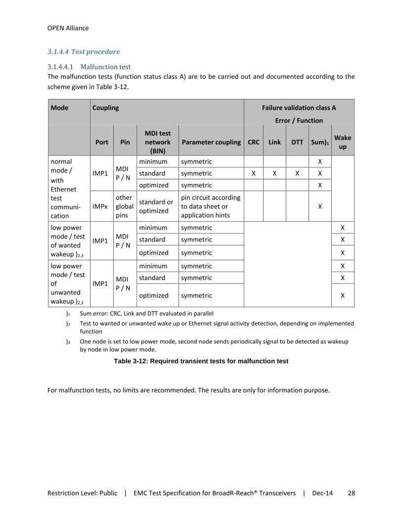
3.1.4.4 Test procedure
3.1.4.4.1 Malfunction test
The malfunction tests (function status class A) are to be carried out and documented according to the
scheme given in Table 3-12.
Mode Coupling Failure validation class A
Error / Function
Port Pin
MDI test network
(BIN) Parameter coupling CRC Link DTT Sum)1
Wake up
normal mode /
with Ethernet test communi-cation
IMP1 MDI P / N
minimum symmetric X
standard symmetric X X X X
optimized symmetric X
IMPx other global pins
standard or optimized
pin circuit according to data sheet or application hints
X
low power mode / test of wanted wakeup )2,3
IMP1 MDI P / N
minimum symmetric
X
standard symmetric X
optimized symmetric X
low power mode / test of unwanted wakeup )2,3
IMP1 MDI P / N
minimum symmetric X
standard symmetric X
optimized symmetric X
)1 Sum error: CRC, Link and DTT evaluated in parallel
)2 Test to wanted or unwanted wake up or Ethernet signal activity detection, depending on implemented function
)3 One node is set to low power mode, second node sends periodically signal to be detected as wakeup by node in low power mode.
Table 3-12: Required transient tests for malfunction test
For malfunction tests, no limits are recommended. The results are only for information purpose.

OPEN Alliance
Restriction Level: Public | EMC Test Specification for BroadR-Reach® Transceivers | Dec-14 29
3.1.4.4.2 Damage test
The damage tests are to be carried out and documented according to the scheme given in Table 3-13. The
fault criteria are evaluated after each single test.
Mode Coupling Failure validation class
Port Pin MDI test network (BIN)
Parameter coupling
normal mode
/ with
Ethernet test
communi-
cation
IMP1 MDI
P / N
standard or
optimized symmetric
C or D
must be stated as test
result IMPx
other
global
pins
standard or
optimized
pin circuit according to
data sheet or application
hints
Table 3-13: Required transient tests for damage test
Recommended limits are given in Appendix C.3.
OPEN Alliance
Restriction Level: Public | EMC Test Specification for BroadR-Reach® Transceivers | Dec-14 30
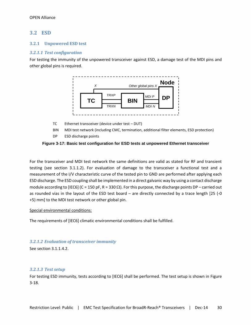
3.2 ESD
3.2.1 Unpowered ESD test
3.2.1.1 Test configuration
For testing the immunity of the unpowered transceiver against ESD, a damage test of the MDI pins and
other global pins is required.
MDI N
Node
TC BIN TRXP
TRXN
DP
Other global pins X
MDI P
X
TC Ethernet transceiver (device under test – DUT)
BIN MDI test network (including CMC, termination, additional filter elements, ESD protection)
DP ESD discharge points
Figure 3-17: Basic test configuration for ESD tests at unpowered Ethernet transceiver
For the transceiver and MDI test network the same definitions are valid as stated for RF and transient
testing (see section 3.1.1.2). For evaluation of damage to the transceiver a functional test and a
measurement of the I/V characteristic curve of the tested pin to GND are performed after applying each
ESD discharge. The ESD coupling shall be implemented in a direct galvanic way by using a contact discharge
module according to [IEC6] (C = 150 pF, R = 330 ). For this purpose, the discharge points DP – carried out
as rounded vias in the layout of the ESD test board – are directly connected by a trace length [25 (-0
+5) mm] to the MDI test network or other global pin.
Special environmental conditions:
The requirements of [IEC6] climatic environmental conditions shall be fulfilled.
3.2.1.2 Evaluation of transceiver immunity
See section 3.1.1.4.2.
3.2.1.3 Test setup
For testing ESD immunity, tests according to [IEC6] shall be performed. The test setup is shown in Figure
3-18.
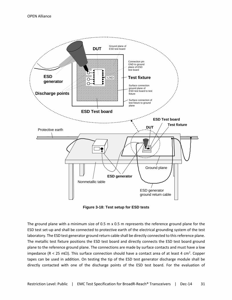
OPEN Alliance
Restriction Level: Public | EMC Test Specification for BroadR-Reach® Transceivers | Dec-14 31
Ground plane
Protective earth
ESD generator
ESD generator ground return cable
Test fixture
ESD Test board
DUT
Nonmetallic table
ESD Test board
GND
Discharge points
Ground plane of ESD test board
Connection pin GND to ground plane of ESD test board
Test fixture
Surface connection ground plane of ESD test board to test fixture
Surface connection of test fixture to ground plane
DUT
ESD generator
Figure 3-18: Test setup for ESD tests
The ground plane with a minimum size of 0.5 m x 0.5 m represents the reference ground plane for the
ESD test set-up and shall be connected to protective earth of the electrical grounding system of the test
laboratory. The ESD test generator ground return cable shall be directly connected to this reference plane.
The metallic test fixture positions the ESD test board and directly connects the ESD test board ground
plane to the reference ground plane. The connections are made by surface contacts and must have a low
impedance (R < 25 m). This surface connection should have a contact area of at least 4 cm2. Copper
tapes can be used in addition. On testing the tip of the ESD test generator discharge module shall be
directly contacted with one of the discharge points of the ESD test board. For the evaluation of

OPEN Alliance
Restriction Level: Public | EMC Test Specification for BroadR-Reach® Transceivers | Dec-14 32
functionality of tested transceiver after each single test a specific test extension frame may be used for
this purpose for contacting the ESD test board.
Test equipment requirements:
ESD test generator: according to [IEC6]; contact discharge module with discharge
capacitor 150 pF and discharge resistor 330
ESD test board: according to Appendix A
Second Ethernet node
system: used for functional testing after ESD discharge
Semiconductor
parameter analyzer: used for I/V measurement after ESD discharge
OPEN Alliance
Restriction Level: Public | EMC Test Specification for BroadR-Reach® Transceivers | Dec-14 33
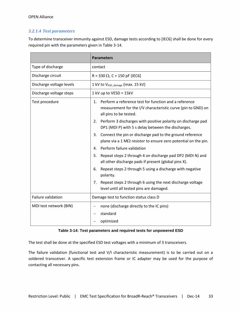
3.2.1.4 Test parameters
To determine transceiver immunity against ESD, damage tests according to [IEC6] shall be done for every
required pin with the parameters given in Table 3-14.
Parameters
Type of discharge contact
Discharge circuit R = 330 , C = 150 pF [IEC6]
Discharge voltage levels 1 kV to VESD_damage (max. 15 kV)
Discharge voltage steps 1 kV up to VESD = 15kV
Test procedure 1. Perform a reference test for function and a reference
measurement for the I/V characteristic curve (pin to GND) on
all pins to be tested.
2. Perform 3 discharges with positive polarity on discharge pad
DP1 (MDI P) with 5 s delay between the discharges.
3. Connect the pin or discharge pad to the ground reference
plane via a 1 M resistor to ensure zero potential on the pin.
4. Perform failure validation
5. Repeat steps 2 through 4 on discharge pad DP2 (MDI N) and
all other discharge pads if present (global pins X).
6. Repeat steps 2 through 5 using a discharge with negative
polarity.
7. Repeat steps 2 through 6 using the next discharge voltage
level until all tested pins are damaged.
Failure validation Damage test to function status class D
MDI test network (BIN) none (discharge directly to the IC pins)
standard
optimized
Table 3-14: Test parameters and required tests for unpowered ESD
The test shall be done at the specified ESD test voltages with a minimum of 3 transceivers.
The failure validation (functional test and V/I characteristic measurement) is to be carried out on a
soldered transceiver. A specific test extension frame or IC adapter may be used for the purpose of
contacting all necessary pins.

OPEN Alliance
Restriction Level: Public | EMC Test Specification for BroadR-Reach® Transceivers | Dec-14 34
3.2.1.5 Test procedure for damage test
The damage tests are to be carried out and documented according to the scheme given in Table 3-15. The
fault criteria are evaluated after each single test.
Coupling Failure validation class
Points Pin MDI test network (BIN)
Parameter coupling
DP1,2 MDI P / N
none
(discharge direct
to IC pins)
direct, contact discharge
D
standard direct, contact discharge
optimized direct, contact discharge
DPx
other
global pins
standard or
optimized
direct, contact discharge,
external pin circuit
according to data sheet
or application hints
Table 3-15: Required tests for unpowered ESD
Recommended limits are given in Appendix C.4.

OPEN Alliance
Restriction Level: Public | EMC Test Specification for BroadR-Reach® Transceivers | Dec-14 35
3.2.2 Powered ESD test
3.2.2.1 Test configuration
For testing the immunity of the powered transceiver against ESD, a damage test of the MDI pins is
required.
Counterpart node
µC
TC µC BIN
Enhanced MII interfaces
TC BIN
Host µC board Transceiver ESD board
MII interface
MII interface
Voltage supply
Voltage supply
MDI P
MDI N
DP
TC Ethernet transceiver (device under test – DUT)
BIN MDI test network (including CMC, termination, additional filter elements, ESD protection)
DP ESD discharge points
Figure 3-19: Basic test configuration for ESD tests at powered Ethernet transceiver
For the transceiver and MDI test network the same definitions are valid as stated for RF and transient
testing (see section 3.1.1.2). For testing the powered transceiver a second counterpart node is used for
communication test.
All other definitions of section 3.2.1.1 are valid.
3.2.2.2 Evaluation of transceiver immunity
See section 3.1.1.4.2.
3.2.2.3 Test setup
See section 3.2.1.3.
OPEN Alliance
Restriction Level: Public | EMC Test Specification for BroadR-Reach® Transceivers | Dec-14 36
3.2.2.4 Test parameters
To determine the immunity against ESD of the powered transceiver, tests according to [IEC6] shall be done
for the MDI pins with the parameters given in Table 3-16.
Parameters
Type of discharge contact
Discharge circuit R = 330 , C = 150 pF [IEC6]
Discharge voltage levels 1 kV to VESD_damage (max. 15 kV)
Discharge voltage steps 1 kV up to VESD = 15kV
Test procedure 1. Perform a reference test for function and a reference
measurement for the I/V characteristic curve (pin to GND) on
all pins to be tested.
2. Perform 3 discharges with positive polarity on discharge pad
DP1 (MDI P) with 5 s delay between the discharges.
3. Connect the pin or discharge pad to the ground reference
plane via a 1 M resistor to ensure zero potential on the pin.
4. Perform failure validation
5. Repeat steps 2 through 4 on discharge pad DP2 (MDI N)
6. Repeat steps 2 through 5 using a discharge with negative
polarity.
Table 3-16: Test parameters and required tests for powered ESD
The test shall be done at the specified ESD test voltages with a minimum of 3 transceivers.
3.2.2.5 Test procedure for damage test
The tests are to be carried out and documented according to the scheme given in Table 3-17. The fault
criteria are evaluated after each single test.

OPEN Alliance
Restriction Level: Public | EMC Test Specification for BroadR-Reach® Transceivers | Dec-14 37
Coupling Failure validation class
Points Pin MDI test network (BIN)
Parameter coupling
DP1,2 MDI P / N standard or
optimized direct, contact discharge
C or D
must be stated as test
result
Table 3-17: Required tests for powered ESD
Recommended limits are given in Appendix C.4.
OPEN Alliance
Restriction Level: Public | EMC Test Specification for BroadR-Reach® Transceivers | Dec-14 38
Appendix A - Test circuit boards
A.1 RF and transient tests
A printed circuit board shall be used for RF and transient tests with the used node to node network. To
ensure good RF parameters of the coupling and measuring networks, a PCB with at least four layers should
be used. The length of the coupling paths on the test board should be kept as short as possible. The
insertion losses of the DPI coupling ports as well as the 150 Ohm emission ports to the respective
transceiver signal pads of the test board shall be measured and documented in the test report.
Examples for test board for the Ethernet node to node network:
Figure A-1: Example RF and transient test board system for BroadR-Reach® transceiver, consisting of Host µC board, Enhanced MII interface and Transceiver RF board

OPEN Alliance
Restriction Level: Public | EMC Test Specification for BroadR-Reach® Transceivers | Dec-14 39
Example for definition of enhanced MII interface between Host µC board and Transceiver RF board used
for the Ethernet node to node network:
Use connector : Samtec - ERM8-030-01-L-D-EM2-L and ERF8-030-05.0-L-DV-L-TR
Figure A-2: Example for definition of enhanced MII interface between Host µC board and Transceiver RF board used for the Ethernet node to node network
Pin Signal Signal Pin
1 GND VCC(3.3V) 2
3 GND VCC(3.3V) 4
5 GND GND 6
7 GND MDC 8
9 GND MDIO 10
11 GND GND 12
13 GND CRS 14
15 GND COL 16
17 GND GND 18
19 GND RXD3 20
21 GND RXD2 22
23 GND RXD1 24
25 GND RXD0 26
27 GND GND 28
29 GND RX_CLK 30
31 GND RX_DV 32
33 GND GND 34
35 GND TX_CLK 36
37 GND GND 38
39 GND TXD3 40
41 GND TXD2 42
43 GND TXD1 44
45 GND TXD0 46
47 GND GND 48
49 GND TX_EN 50
51 GND GND 52
53 SF1 *) TX_ER 54
55 SF2 *) RX_ER 56
57 SF3 *) GND 58
59 SF4 *) Reset 60

OPEN Alliance
Restriction Level: Public | EMC Test Specification for BroadR-Reach® Transceivers | Dec-14 40
A.2 ESD tests
For ESD tests a printed circuit board shall be used. A four-layer construction of the PCB shall be chosen
with extensive ground area. The pads for the discharge points DPx are to be carried out in such a way that
a safe contact to the discharge tip of the testing generator is guaranteed. The passive components of the
minimal wiring network shall be placed in direct proximity of the transceiver.
The insulation distance between the signal lines and pads of the passive components and the extensive
ground area should be chosen in such a way, that a disruptive discharge at a test voltage of 8 kV is
impossible at these points.
Further requirements apply to the ESD test board:
Trace length between pads MDI test network and
discharge point: 25 (-0 + 5) mm
Track width of the conducting path: 0,254mm (10 mil)
Substrate material: FR4
Thickness substrate: 1.5mm
The test adapter used for functional and leakage current examination makes direct contacting of the
transceiver pins possible.
Examples for ESD test board for Ethernet transceiver:
Figure A-3: Example ESD test board for Ethernet transceiver
OPEN Alliance
Restriction Level: Public | EMC Test Specification for BroadR-Reach® Transceivers | Dec-14 41
Appendix B - Required information from semiconductor manufacturer
The following information is required for setting up and doing the EMC tests at BroadR-Reach 100 Mbit/s
transceivers and shall be supported by the semiconductor manufacturer:
test circuit for typical application of transceiver according to section 3.1.1.2 (standard MDI test
network)
software configuration data for setting the transceiver in typical application according to section 0
detailed information for data transmission and error register read out activity.
The following additional information should be supported by the semiconductor manufacturer, if
available or needed respectively:
EMC optimized test circuit (optimized MDI test network and optimized filter or supplier specific
filter at voltage supply pins)
information for ESD protection devices
layout application hints or equivalent layout requirements
software configuration data for setting the transceiver in EMC optimized state.
OPEN Alliance
Restriction Level: Public | EMC Test Specification for BroadR-Reach® Transceivers | Dec-14 42
Appendix C – Recommended limits for tests
C.1 Emission of RF disturbances
For evaluation of RF emissions at the MDI, other global pins and voltage supply pins the limits given in
Figure C-0-1 are recommended.
Figure C-0-1: Recommended limits for RF emission
0
10
20
30
40
50
60
70
80
0,1 1 10 100 1000
Limit MDI, other global pins
Limit local pins (voltage supplies)
150 Ohm Emission Measurement - OA BroadRReachDetector: Peak
[MHz]
[dBµV]
76 MHz50 MHz10 MHz0.75 MHz0.3 MHz

OPEN Alliance
Restriction Level: Public | EMC Test Specification for BroadR-Reach® Transceivers | Dec-14 43
C.2 Immunity to RF disturbances
For evaluation of RF immunity of the MDI and other global pins the limits given in Figure C-0-2 for damage
tests and Figure C-0-3 for malfunction tests are recommended.
Figure C-0-2: Recommended limits for RF immunity damage tests
Figure C-0-3: Recommended limits for RF immunity malfunction tests
10
15
20
25
30
35
40
45
1 10 100 1000
Limit MDI / Damage
Limit other global pins / Damage
[MHz]
[dBm]
DPI Test - OA BroadRReachRF coupling: MDI, other global pins - AM
88 MHz8 MHz
10
15
20
25
30
35
40
45
1 10 100 1000
Limit MDI / Malfunction
Limit other global pins / Malfunction
[MHz]
[dBm]
88 MHz8 MHz
DPI Test - OA BroadRReachRF coupling: MDI - AM / other global pins - CW, AM

OPEN Alliance
Restriction Level: Public | EMC Test Specification for BroadR-Reach® Transceivers | Dec-14 44
C.3 Immunity to transients
For evaluation of transient immunity of the MDI and other global pins only limits for damage are
recommended:
Test pulse Vs [V]
1 - 100
2a + 75
3a - 150
3b + 100
Table C-1: Recommended voltage levels for transient immunity to damage
C.4 ESD
For ESD immunity to damage of the MDI and other global pins +/- 6 kV are recommended.
=== END OF DOCUMENT ===