generic ic emc test specification - zvei.org · may 2017 german electrical and electronic...
TRANSCRIPT
May 2017
German Electrical and Electronic Manufacturers´ Association
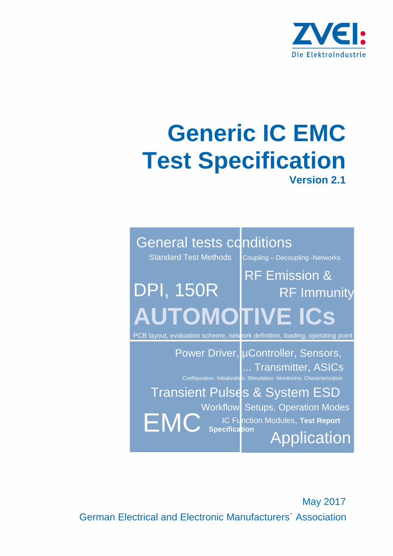
Generic IC EMC Test Specification
Version 2.1
General tests conditions Standard Test Methods Coupling – Decoupling -Networks
DPI, 150R
AUTOMOTIVE ICs PCB layout, evaluation scheme, network definition, loading, operating point
Power Driver, µController, Sensors,
... Transmitter, ASICs Configuration, Initialization, Stimulation, Monitoring, Characterization
Transient Pulses & System ESD Workflow, Setups, Operation Modes
IC Function Modules, Test Report
RF Emission &
RF Immunity
EMC Specification Application

2
Imprint
Generic IC EMC Test Specification Version 2.1 Published by: ZVEI - German Electrical and Electronic Manufacturers’ Association Electrical Components and Systems Division Lyoner Strasse 9 60528 Frankfurt am Main, Germany
Responsible: Dr.-Ing. Rolf Winter Phone: +49 69 6302-402 E-mail: [email protected] Authors: This specification version 2.1 was created by the following company’s experts, Robert Bosch GmbH: Dr. Wolfgang Pfaff, Michael Bischoff, Frank Brandl, Dr. Carsten Hermann, Infineon Technologies AG: Dr. Frank Klotz, Thomas Steinecke, Markus Unger Continental Automotive GmbH: Felix Müller, Christian Rödig, Gerhard Schmid. July 2017 Conditions of use:
This document may be reproduced free of charge in any format or medium provided it is reproduced accurately and is not used in a misleading context.
This document may also be revised and reproduced in a revised form, provided that any changes have been made visible as such.
Every effort was made to ensure that the information given herein is accurate, but no legal responsibility is accepted for any errors, omissions or misleading statements in this information.
The document can be found at: http://www.zvei.org/generic-ic-emc-test-specification
3
1 SCOPE .........................................................................................................................6
2 NORMATIVE REFERENCE .........................................................................................7
2.1 International standards ....................................................................................7 2.2 Other relevant documents ...............................................................................8 2.3 Internet references ...........................................................................................8
3 DEFINITIONS AND ABBREVIATIONS .......................................................................9
3.1 Definitions .........................................................................................................9 3.2 Abbreviations ................................................................................................. 11
4 GENERAL ................................................................................................................. 12
4.1 Objective ......................................................................................................... 12 4.2 Workflow for selection and test ................................................................... 13
5 TEST DEFINITIONS .................................................................................................. 14
5.1 Test methods ................................................................................................. 14 5.1.1 Conducted RF test methods ......................................................................... 14 5.1.2 Radiated RF test methods ............................................................................ 14 5.1.3 Transient pulse test methods ....................................................................... 14 5.1.4 ESD Test methods ....................................................................................... 14
5.2 Test parameters ............................................................................................. 15 5.2.1 General test conditions ................................................................................. 15 5.2.2 RF Emission: Bandwidths and frequency step sizes ................................... 15 5.2.3 Immunity against RF disturbances ............................................................... 16 5.2.4 Immunity against transient pulses ................................................................ 17 5.2.5 Immunity against ESD .................................................................................. 18
6 IC FUNCTION MODULES ......................................................................................... 19
6.1 General ........................................................................................................... 19 6.2 Port module .................................................................................................... 19 6.3 Supply module ............................................................................................... 20 6.4 Core module ................................................................................................... 21 6.5 Oscillator module .......................................................................................... 22 6.6 Splitting ICs into IC function modules ........................................................ 23
6.6.1 Matrix for splitting ICs ................................................................................... 23 6.6.2 Example of an IC built up with IC function modules ..................................... 24
7 SELECTION GUIDE FOR TEST CONFIGURATION ............................................... 25
7.1 Conducted tests............................................................................................. 25 7.1.1 Pin selection for conducted RF emission and RF immunity tests ................ 25 7.1.2 Coupling and injection points ....................................................................... 25 7.1.3 Configuration for conducted RF emission tests ........................................... 26 7.1.4 Configuration for conducted RF immunity tests ........................................... 27 7.1.5 Pin selection for conducted transient pulse immunity tests .......................... 28 7.1.6 Configuration for conducted transient pulse immunity tests......................... 30 7.1.7 Pin selection for unpowered system level ESD tests ................................... 31 7.1.8 Configuration for unpowered system level ESD tests .................................. 31
7.2 Radiated tests ................................................................................................ 31 7.2.1 Criteria for performing radiated emission and immunity tests ...................... 31 7.2.2 Test configuration for radiated emission ...................................................... 31 7.2.3 Test configuration for radiated immunity ...................................................... 31
8 TEST AND MEASUREMENT NETWORKS ............................................................. 32
8.1 Emission and immunity tests ....................................................................... 32 8.1.1 Port module .................................................................................................. 32
8.1.1.1 Line driver ............................................................................................... 32
8.1.1.2 Line receiver ........................................................................................... 34

4
8.1.1.3 Symmetrical line driver ............................................................................ 35
8.1.1.4 Symmetrical line receiver ........................................................................ 36
8.1.1.5 Regional driver ........................................................................................ 37
8.1.1.6 Regional input ......................................................................................... 39
8.1.1.7 High side driver ....................................................................................... 40
8.1.1.8 Low side driver ........................................................................................ 42
8.1.1.9 RF antenna driver ................................................................................... 45
8.1.1.10 RF antenna receiver ............................................................................... 45
8.1.2 Supply module .............................................................................................. 46 8.1.3 Core module ................................................................................................. 48 8.1.4 Oscillator module .......................................................................................... 48
8.2 ESD test .......................................................................................................... 49 8.2.1 Test network for unpowered system level ESD tests ................................... 49
9 TEST SETUP ............................................................................................................. 50
9.1 Signal decoupling for stimulus and monitoring ......................................... 50 9.1.1 Stimulus setup .............................................................................................. 50 9.1.2 DUT Monitoring ............................................................................................ 50 9.1.3 Monitoring setup ........................................................................................... 51 9.1.4 Performance classes for immunity testing.................................................... 52
9.2 (G)TEM-cell setup .......................................................................................... 53 9.3 IC stripline setup............................................................................................ 53 9.4 System level ESD test setup ........................................................................ 54 9.5 Test board ...................................................................................................... 54
9.5.1 General ......................................................................................................... 54 9.5.2 RF emission and immunity ........................................................................... 54 9.5.3 Transient pulses ........................................................................................... 55 9.5.4 System level ESD ......................................................................................... 55
10 FUNCTIONAL CONFIGURATIONS AND OPERATING MODES ............................ 56
10.1 Test configuration for ICs without CPU ...................................................... 56 10.1.1 Emission test configuration .......................................................................... 56 10.1.2 Immunity and transient test configuration..................................................... 58
10.2 Test configuration for ICs with CPU ............................................................ 60 10.2.1 Software initialization for emission tests....................................................... 60 10.2.2 Software initialization for immunity and transient voltage tests .................... 63 10.2.3 Software loop ................................................................................................ 65
11 EMC LIMITS FOR AUTOMOTIVE ICS ..................................................................... 66
11.1 RF emission ................................................................................................... 66 11.1.1 Emission level scheme ................................................................................. 66 11.1.2 General emission limit classes ..................................................................... 67 11.1.3 Emission limits for microcontrollers with external digital bus systems ......... 71
11.2 RF immunity ................................................................................................... 74 11.2.1 General immunity limit classes ..................................................................... 74
11.3 Pulse immunity .............................................................................................. 76 11.3.1 Preliminary pulse immunity limit classes 12 V ............................................. 76 11.3.2 Preliminary pulse immunity limit classes 24V .............................................. 76
11.4 System level ESD .......................................................................................... 77 11.4.1 Preliminary limits for unpowered system level ESD test .............................. 77
12 IC EMC SPECIFICATION ......................................................................................... 78
13 TEST REPORT .......................................................................................................... 78
14 CONTACTS AND AUTHORS ................................................................................... 79
5
ANNEX A TEST NETWORK MODIFICATION (EMISSION, NORMATIVE).................... 80
A.1 Start frequency calculation .......................................................................... 80
ANNEX B TEST DEFINITION FOR ICS WITH RF ANTENNA PINS (NORMATIVE) .... 81
B.1 General ........................................................................................................... 81 B.2 GTEM-cell test board and setup for ICs with RF antenna port ................. 81
B.2.1 Radiated emission test ................................................................................. 81 B.2.2 Radiated immunity test ................................................................................. 82 B.2.3 Positioning and naming of the DUT in GTEM cell ........................................ 82
ANNEX C LAYOUT RECOMMENDATION (INFORMATIVE) ......................................... 84
C.1 Several networks ........................................................................................... 84 C.1.1 Layout example of 150 networks on 2 layer and multi layer PCB ............ 84 C.1.2 Layout example of 1 network on 2 layer and multi layer PCB .................. 84 C.1.3 Layout example of DPI network on 2 layer and multi layer PCB.................. 85 C.1.4 Layout Example of a TEM cell test board..................................................... 85 C.1.5 Layout example for systems with IC types microcontroller, RAM and flash 86
C.2 Multi method test board ................................................................................ 86 C.3 Example of multi method test board for microcontrollers ........................ 86
C.3.1 Component side (top layer, components, power planes) ............................. 86 C.3.2 Inner layer 1 (mid layer 1, ground plane): .................................................... 88 C.3.3 Inner layer 2 (mid layer 2, split power planes): ............................................ 88 C.3.4 Inner layer 3 (mid layer 3, ground plane) : ................................................... 89 C.3.5 Inner layer 4 (mid layer 4, signal wiring, split power plane): ........................ 90 C.3.6 Bottom side (DUT, shielding GND for TEM-cell): ......................................... 90
C.4 Layout examples of system level ESD test boards .................................... 91
ANNEX D TRACE IMPEDANCE CALCULATION (INFORMATIVE) .............................. 95
D.1 Equations for calculating micro stripline impedances .............................. 95 D.1.1 Micro stripline ............................................................................................... 95 D.1.2 Symmetrical stripline .................................................................................... 95 D.1.3 Offset stripline ............................................................................................... 96
ANNEX E MODULATION DEFINITION FOR IMMUNITY TESTS (INFORMATIVE) ...... 97
ANNEX F EXAMPLE OF AN IC EMC SPECIFICATION (INFORMATIVE).................... 99
ANNEX G CALCULATION OF PIN SPECIFIC LIMITS (INFORMATIVE).................... 102
G.1 Fourier transformation of time domain signals ........................................ 102
15 LIST OF FIGURES .................................................................................................. 104
16 LIST OF TABLES .................................................................................................... 106
6
1 Scope
This document defines common tests characterising the EMC behaviour of integrated circuits (ICs) in terms of RF emission and RF immunity in the frequency range from 150 kHz up to 3 GHz as well as pulse immunity and system level ESD*), based on international standards for integrated circuits and related standards for IC applications. It contains all information to evaluate any kind of ICs in the same way. In this document general information and definitions of IC types, pin types, test and measurement networks, pin selection, operation modes and limit classes are given. This allows the user to create an EMC specification for a dedicated IC as well as to provide comparable results for comparable ICs.
*) Note: Unpowered system level ESD test covered, powered system level ESD test under consideration

7
2 Normative Reference
2.1 International standards
The following referenced documents are indispensable for the application of this document. For dated references, only the edition cited applies. For undated references, the latest edition of the referenced document (including any amendments) applies.
RF Emission:
[1] IEC 61967-1 Ed. 1: 2002, Integrated circuits – Measurement of electromagnetic emissions 150 kHz to 1 GHz – Part 1: General conditions and definitions
[2] IEC 61967-2 Ed. 1: 2005, Integrated circuits – Measurement of electromagnetic emissions 150 kHz to 1 GHz – Part 2: Measurement of radiated emissions – TEM cell and wideband TEM cell method
[3] IEC 61967-4 Ed. 1: 2006, Integrated circuits – Measurement of electromagnetic emissions 150 kHz to 1 GHz – Part 4: Measurement of conducted emissions –
1 /150 direct coupling method
[4] CISPR 25 3rd Ed. 2008-03: Vehicles, boats and internal combustion engines – Radio disturbance characteristics – Limits and methods of measurement for the protection of on-board receivers
[5] IEC 61967-8 Ed.1: 2011 Integrated Circuits – Measurement of Electromagnetic Emissions Part 8: Measurement of radiated emissions – IC stripline method
RF Immunity:
[6] IEC 62132-1 Ed. 1: 2006, Integrated circuits – Measurement of electromagnetic immunity 150 kHz to 1 GHz – Part 1: General and definitions
[7] IEC 62132-2 Ed. 1: 2010, Integrated circuits – Measurement of electromagnetic immunity 150 kHz to 1 GHz – Part 2: Measurement of radiated immunity – TEM Cell and Wide Band TEM Cell Method
[8] IEC 62132-4 Ed. 1: 2006, Integrated circuits – Measurement of electromagnetic immunity 150 kHz to 1 GHz – Part 4: Direct RF Power Injection Method
[9] IEC 62132-8 Ed. 1:2012, Integrated circuits – Measurement of electromagnetic immunity – Part 8: Measurement of radiated immunity – IC stripline method
Transient voltages:
[10] IEC 62215-3 Ed.1: Integrated circuits – Measurement of impulse immunity – Part 3: Non-synchronous transient injection method
[11] ISO 7637-2 3rd Ed. 2011, Road vehicles – Electrical disturbances from conduction and coupling – Part 2: Electrical transient conduction along supply lines only
[12] ISO 7637-3 2nd Ed. 2007-07-01: Road vehicles – Electrical disturbances from conduction and coupling – Part 3: Electrical transient transmission by capacitive and inductive coupling via lines other than supply lines
Electrostatic discharge:
[13] IEC61000-4-2 2nd Ed. 2008, Electromagnetic compatibility (EMC) – Part 4: Testing and measuring techniques – Section 2: Electrostatic discharge immunity test – Basic EMC publication
[14] ISO 10605 2nd Ed. 2008-07-15: Road vehicles – Test methods for electrical disturbances from electrostatic discharge
[15] EIA JEP155A: 01/2012 Recommended ESD target levels for HBM/MM qualification
[16] EIA JEP157: 10/2009 Recommended ESD-CDM target levels

8
[17] ANSI/ESDA/JEDEC JS-001-2011, Electrostatic Discharge Sensitivity Testing Human Body Model (HBM) – Component Level
[18] JESD22-C101E 12/2009: Field-Induced Charged-Device Model Test Method For Electrostatic Discharge Withstand Thresholds of Microelectronic Components:
2.2 Other relevant documents
[19] IEC 62228 TS Ed. 1: 2007: Integrated circuits – EMC evaluation of CAN transceivers
[20] Hardware Requirements for LIN, CAN and FlexRay Interfaces in Automotive Applications, Version 1.3, 2012
[21] ISO11452-1 Road vehicles — Component test methods for electrical disturbances from narrowband radiated electromagnetic energy — Part 1: General principles and terminology
[22] Hall/Hall/McCall, High Speed Digital System Design, issue 2000, ISBN 0-471-36090-2
2.3 Internet references
[IEV] http://www.electropedia.org/iev/iev.nsf/Welcome?OpenForm&Seq=1

9
3 Definitions and Abbreviations
3.1 Definitions
analog Pertaining to the representation of information by means of a physical quantity which may at any instant within a continuous time interval assume any value within a continuous interval of values. Note: - The quantity considered may, for example, follow continuously the values of another physical quantity representing information.
[IEV 101-12-05]
core
An IC function module without any connection to outside of the IC via pins. (Note: The supply is connected via the IC function module supply to pins, signals to pins are connected via IC function module driver)
digital Pertaining to the representation of information by distinct states or discrete values.
[IEV 101-12-07]
EMC pin type
global pin
A 'global' pin carries a signal or power, which enters or leaves the application board without any active component in between.
local pin
A 'local' pin carries a signal or power, which does not leave the application board. It remains on the application PCB as a signal between two components.
fixed function unit (FFU)
Functional core sub-unit of the IC function module 'Core', designed to perform one fixed function without instruction decoding and executing capability.
function A set of relations which determines the value of the output variable from a given state of a system and the simultaneous value(s) of the input variable(s) [IEV 351-29-08, "Output function"]
IC type
IC with a characteristic set of functions built in. These functions are realized with IC function modules.
IC function module An IC function module is a device functional part of an IC with at least one function and its supply connection, if needed. (see also Figure 1)
Passive IC function module: No supply system for function
Active IC function module: A dedicated supply connection needed for function.
Note: The supply connection is handled as a separate input/output pair as it has a dedicated EMC behavior.

10
supply connection
supply referenceconnection
inputs outputsIC FunctionModule
Figure 1: Common definition of an IC function module
integrated circuit (IC)
An integrated circuit (IC) is a set of implemented IC function modules in one die or package.
mandatory components Mandatory components are components needed for proper function of IC function modules as specified by the IC manufacturer (e.g. application note).
pin Interface between an IC and its circuit environment.
port
An IC function module containing minimum one driver and/or minimum one input each connected to a signal pin.
active port
An active port is initialized to a defined configuration or connected to a fixed-function module unit and is in operating mode during EMC measurements.
inactive port An inactive port is initialized to a defined configuration or connected to a
fixed-function module unit and remains in a defined static mode.
power net Main Power Supply of an application system.
printed circuit board (PCB): A piece of isolating material with fixed metal traces to connect electronic components.
sub supply net Supply Net derived from Power Net.
supply pin pairs Supply pin pairs are all supply voltage pins of the same supply voltage system with their related ground pin(s) of an IC supply module.
system level
Application-like test conditions (e.g. taken from electronic control unit requirements) directly applied on IC pins with or without external components
11
3.2 Abbreviations
AM Amplitude Modulation
BAN Broadband Artificial Network
BW Bandwidth
CAN Controller Area Network
CDM Charged Device Model
CW Continuous Wave
DPI Direct Power Injection
E-Field Electric Field
EMC Electromagnetic Compatibility
ESD Electrostatic Discharge
ETSI European Telecommunications Standards Institute
FCC Federal Communications Commission
FFU Fixed Function Unit
GTEM-Cell Gigahertz Transversal Electromagnetic Wave Cell
IC Integrated Circuit
I/O Input / Output
H-Field Magnetic Field
HBM Human Body Model
HSD High Side Driver
LIN Local Interconnect Network
LNA Low Noise Amplifier
LSD Low Side Driver
LVDS Low Voltage Differential Signalling
LVR Linear Voltage Regulator
PCB Printed Circuit Board
PM Pulse Modulation
RBW Resolution Bandwidth
RF Radio Frequency
SMPS Switched Mode Power Supply
TEM-Cell Transverse Electromagnetic Cell

12
4 General
4.1 Objective
The objective and benefit of the document is
to obtain relevant quantitative IC EMC measurement results
to reduce the number of IC EMC test methods to a necessary minimum
to strengthen the acceptance of IC EMC test results
to minimize EMC test effort to get comparable results for IC suppliers and users
to release ICs based on IC level EMC results

13
4.2 Workflow for selection and test
The following recommended workflow shows in sequential order the steps required to generate a dedicated IC EMC specification and to perform the EMC measurements. A template of the IC EMC specification is provided in Chapter 12.
EMC specification
definition of EMC test requirements and targets
identification of all IC function modules and selection of the EMC relevant modules(as defined in chapter 6)
listing of all related pins and classification in local and global pins (as defined in chapter 6)
selection of pins to be measured (chapter 7.1) and monitored (chapter 9.1.2)
selection of functional configuration, operation mode and software
requirements (as defined in chapter 10)
selection of test- and measurement networks
(as defined in chapter 8)
add radiated test methods, if criteria are met (see chapter 7.2.1)
selection of the test limits and monitoring definition
(as defined in chapter 11 and 9.1.2)
EMC test
design of test schematic and board layout (see chapter 9.5)
performing measurements according to EMC specification (see chapter 12)
test report (see chapter 13)
Table 1: Workflow to perform IC EMC measurements
14
5 Test definitions
5.1 Test methods
5.1.1 Conducted RF test methods
The conducted RF tests have to be performed for all ICs.
test type coupling method method name reference
conducted emission
direct coupling via 150 / 1 network 150 / 1 method IEC61967-4
conducted immunity
direct RF-power injection via DC block capacitor
direct power injection (DPI) IEC62132-4
Table 2: Conducted test methods
5.1.2 Radiated RF test methods
The radiated RF tests have to be performed only for dedicated ICs, see chapter 7.2.1.
test type coupling method method name reference
radiated emission
E- and H-field radiation of entire IC (G)TEM-cell method IEC61967-2
IC stripline IEC61967-8
radiated immunity
E- and H-field radiation on entire IC (G)TEM-cell method IEC62132-2
IC stripline IEC62132-8
Table 3: Radiated test methods
5.1.3 Transient pulse test methods
The transient pulse tests have to be performed for all ICs if transient exposure is expected, see chapter 7.1.5.
test type coupling method method name reference
transient immunity
direct transient coupling non-synchronous transient injection
IEC62215-3 capacitive transient coupling
Table 4: Transient test methods
5.1.4 ESD Test methods
Unpowered system level ESD tests have to be performed only for dedicated IC pins, see chapter 7.1.7.
test type coupling Method model reference
IC level ESD
contact discharge HBM-IC ANSI/ESDA/JEDEC JS-001-2011
IC level ESD
contact discharge CDM JESD22-C101E
system level ESD
contact discharge HBM-System ISO10605 2nd Ed
Table 5: ESD Test methods

15
5.2 Test parameters
5.2.1 General test conditions
Environment: Temperature 23°C +/-5°C
Supply: Nominal voltage +/- 5%
5.2.2 RF Emission: Bandwidths and frequency step sizes
For all measurements the noise floor must be minimum 6 dB below the limit.
method frequency range receiver****)
RBW step size
1
15
0
µT
EM
GT
EM
***
)
IC s
trip
line 150 kHz to 30 MHz 9 kHz / 10 kHz 4,5 / 5 kHz
30 MHz to 200 MHz
100 kHz / 120 kHz**) 50 / 60 kHz *) 200 MHz to 1000 MHz
1000 MHz to 3000 MHz
Table 6: General test parameters: Emission with RF receiver
*) Note: Upper frequency range of 1 method is critical to handle, see layout recommendations **) Note: Instead of 120 kHz / 100 kHz a bandwidth of 10 kHz / 9 kHz (with appropriate step size) can be
used to reduce the noise level in case of no difference of the disturbances. ***) Note: The GTEM cell can be used above 3 GHz for homologation of transmitter applications according to
ETSI and FCC specifications ****) Note: Time domain FFT analyzers can also be used if the results are identical
method frequency range analyzer
RBW sweep time**)
1
15
0
µT
EM
GT
EM
***
*)
IC s
trip
line
150 kHz to 30 MHz 9 kHz / 10 kHz
RBW
FRLT NP st
30 MHz to 200 MHz
100 kHz / 120 kHz***) *) 200 MHz to 1000 MHz
1000 MHz to 3000 MHz
Table 7: General test parameters: Emission with RF analyser
*) Note: Upper frequency range of 1 method is critical to handle, see layout recommendations **) Note: NP = Number of Points; LT = Loop time or minimum period; FT = Frequency range ***) Note: Instead of 120 kHz / 100 kHz a bandwidth of 10 kHz / 9 kHz (with appropriate step size) can be
used to reduce the noise level in case of no difference of the disturbances. ****) Note: The GTEM cell can be used above 3 GHz for homologation of transmitter applications according to
ETSI and FCC specifications
Detector type: Peak detector
Measurement time: The emission measurement time at one frequency shall be minimal the period or test software loop time (LT).
16
5.2.3 Immunity against RF disturbances
Frequency step sizes
Frequency step sizes related to frequency ranges are shown in Table 8. Critical frequencies such as clock frequencies, system frequencies of RF devices etc. should be tested using smaller frequency steps agreed by the users of this procedure. Deviations have to be stated in the test report.
method frequency range step size
linear
DP
I
µT
EM
GT
EM
*)
IC s
trip
line
150 kHz to 1 MHz 100 kHz
1 MHz to 10 MHz 0,5 MHz
10 MHz to 100 MHz 1 MHz
100 MHz to 200 MHz 2 MHz
200 MHz to 400 MHz 4 MHz
400 MHz to 1000 MHz 10 MHz
1000 MHz to 3000 MHz 20 MHz
Table 8: General test parameters for immunity
*) Note: The GTEM cell can be used above 3 GHz for homologation of transmitter applications according to ETSI standards and FCC rules
Dwell time
at each frequency should be set according to the loop time but at least 1000 ms.
DPI immunity result diagram
shows the maximum applied RF forward power without any monitored failures.
(G)TEM or IC stripline immunity result diagram
shows the maximum applied field strength calculated from the forward power (substitution method) without any monitored failures.
Modulation definition
Modulation frequency range
150 kHz – 800 MHz 800 MHz – 3000 MHz
CW A
AM B
PM B
Table 9: Modulation frequency ranges
A: The continuous wave (CW) test is mandatory.
B: A modulation test (AM, PM) is optional.
Amplitude modulation:
Parameters: 1 kHz, 80%, according to ISO 11452-1 automotive specifications: reduced carrier for same peak CW and AM (see Annex E). The frequency range is 150 kHz up to 800 MHz.
17
CW
equal peak value
AM 80 %
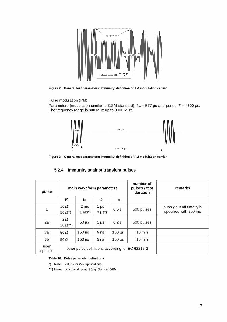
Figure 2: General test parameters: Immunity, definition of AM modulation carrier
Pulse modulation (PM):
Parameters (modulation similar to GSM standard): ton = 577 μs and period T = 4600 μs. The frequency range is 800 MHz up to 3000 MHz.
CWCW off
t = 577 µs
t = 4600 µs
Figure 3: General test parameters: Immunity, definition of PM modulation carrier
5.2.4 Immunity against transient pulses
pulse main waveform parameters
number of pulses / test
duration remarks
Ri td tr t1
1 10
50 *)
2 ms
1 ms*)
1 µs
3 µs*) 0,5 s 500 pulses
supply cut off time t2 is specified with 200 ms
2a 2
10 **) 50 µs 1 µs 0,2 s 500 pulses
3a 50 150 ns 5 ns 100 µs 10 min
3b 50 150 ns 5 ns 100 µs 10 min
user specific
other pulse definitions according to IEC 62215-3
Table 10: Pulse parameter definitions
*) Note: values for 24V applications
**) Note: on special request (e.g. German OEM)

18
5.2.5 Immunity against ESD
pins model
component values
standard ESD level remark
C R
all pins HBM 100 pF 1500 Ω ANSI/ESDA/JEDEC JS-001-
2011
≤ 1 kV*)
or customer specific
IC level ESD test
(for information, not part of this specification) all pins CDM IC specific JESD22-C101E
≤ 250 V*)
or customer specific
global pins
HBM 150 pF 330 Ω ISO10605 2nd Ed.
2 kV
4 kV
6 kV
or customer specific
system level ESD test
Table 11: ESD test definition
*) Note: Recommended ESD levels HBM acc. to JEDEC Publication 155A (JEP 155A)
and CDM JEDEC Publication 157 (JEP 157)
To derive a statistical result at least 3 samples have to be tested. If a higher sample number is preferred for e.g. test automation a certain number of samples for each test level can be used as well.
# Step implementation remark
1 pre-
measurement e.g. DC sweep over DC operating conditions, full
parameter test, …
“0-point” measurement with defined max. current condition
e.g.10 µA
2 pre-charge prevention
Rd ≥ 220 kΩ at all pins under test to GND implemented on PCB
ensure no pre-charging of the pin under test prior testing
3 start level +/- 1 kV default, if not otherwise
specified
4 number of
pulses 3 pulses of each polarity
with discharge after each single pulse for analyses 3 pulses of one
polarity recommended
5 discharge of
pin under test Rd ≥ 220 kΩ at all pins under test to GND
implemented on PCB min. 1 sec. discharge time
between pulses
6 post-
measurement e.g. DC sweep over DC operating conditions, full
parameter test, … once for each test level
7 voltage step 1 kV default, if not otherwise
specified
8 Loop repetition of steps 2 to 7 till max. test voltage level
or failure criteria is reached
Table 12: Test procedure system level ESD

19
6 IC function modules
6.1 General
To define the relevant IC function modules influencing the EMC behaviour of an IC significantly all integrated functions have to be classified according to the following definitions.
6.2 Port module
A port consists of minimum one port module as defined below.
Supply module
CoreSupply
Core
PortSupply module
PortSupply
Driver orInput
Driver orInput
Driver orInput
Driver orInput
Digital Logicor analogFixed-function Unit
Digital Logicor analogFixed-function Unit
Digital Logicor analogFixed-function Unit
Digital Logicor analogFixed-function Unit
Oscillator(PLL)
Supply module
OscillatorSupply
PLL factor
Figure 4: Port module
Port modules are:
a) Line driver
drives a signal leaving the application board (global pin). Examples: ISO9141 outputs, LIN outputs, RF outputs
b) Line receiver
receives a signal from outside of the application board (global pin). Examples: ISO9141 inputs, LIN inputs, RF inputs
c) Symmetrical line driver
drives a differential signal leaving the application board with two phase-correlated outputs (global pin). Examples: CAN outputs, LVDS outputs
d) Symmetrical line receiver
receives a differential signal from outside of the application board with two phase-correlated inputs (global pin). Examples: CAN inputs, LVDS inputs
e) Regional driver
drives a signal not leaving the application board (local pin). Examples: serial data outputs, operational amplifier outputs, RF outputs

20
f) Regional input
receives a signal from the application board (local pin). Examples: serial data inputs, Input stages of operational amplifiers, analog-digital-Converter (ADC) inputs, RF inputs
g) High side driver
drives power into loads. The current flows out of the driver (local or global pin). Examples: High side switch, Switched mode power supply current output (buck converter)
h) Low side driver
drives power into loads. The current flows into the driver (local or global pin). Examples: Low side switch, Switched mode power supply current input (boost converter)
i) RF antenna driver
drives a radio frequency signal into an antenna matching circuitry. Example: RF amplifier
j) RF antenna receiver
receives an RF signal via an antenna matching circuitry. Example: Low noise amplifier (LNA)
6.3 Supply module
A supply module distributes supply current to at least one IC function module (local or global pin).
It is an IC function module with at least one current input pin of the same supply system and minimum one current output. It may contain active elements like voltage stabilization and/or passive elements like internal charge buffering, current limiting elements etc.
Supply module
CoreSupply
Supply module
PortSupply
Driver orInput
Driver orInput
Driver orInput
Driver orInput
Digital Logicor analogFixed-function Unit
Digital Logicor analogFixed-function Unit
Digital Logicor analogFixed-function Unit
Digital Logicor analogFixed-function Unit
Oscillator(PLL)
Supply module
OscillatorSupply
PLL factor
Figure 5: Supply module

21
6.4 Core module
A core module is an IC function module without any connection to outside of the IC via pins. The core is supplied via the IC function module supply. It contains a set of minimum one core module described below.
Supply module
CoreSupply
Core
Supply module
PortSupply
Driver orInput
Driver orInput
Driver orInput
Driver orInput
Digital Logicor analogFixed-function Unit
Digital Logicor analogFixed-function Unit
Digital Logicor analogFixed-function Unit
Digital Logicor analogFixed-function Unit
Oscillator(PLL)
Supply module
OscillatorSupply
PLL factor
Figure 6: Core module
Core modules are:
Central processing unit (CPU)
A CPU decodes and executes instructions, can make decisions and jump to a new set of instructions based on those decisions. Sub-units within the CPU decode and execute instructions (Sub-Unit CU (Control Unit)) and perform arithmetic and logical operations (Sub-Unit ALU (Arithmetic/Logic Unit)), making use of small number-holding areas called registers.
Digital logic fixed-function unit
Functional core sub-unit, designed to perform one fixed core digital logic function without instruction decode and execute capability. Examples: Clock distribution, Memory logic and arrays, Registers, Timer,
Watchdog Timer, State Machines, Programmable Logic Arrays (PLA).
Analog fixed-function unit
Functional core analog sub-unit, clocked or unclocked, designed to perform one fixed core analog function without instruction decode and execute capability. Examples: Analog-to-digital-converter (ADC), Digital-to-analog-converter
(DAC), Sample-and-hold-circuits, Switched capacitor filter, Charge Coupled Devices (CCDs).
22
Dedicated analog fixed function unit: Sensor element
A sensor element is a converter of an environmental value into an electrical value and therefore a FFU.
Examples: Hall sensor element for magnetic field sensing, E-field sensing, Acceleration sensing. It can be combined with a precision amplifier (FFU), a supply module and a line driver to realize an IC type "sensor".
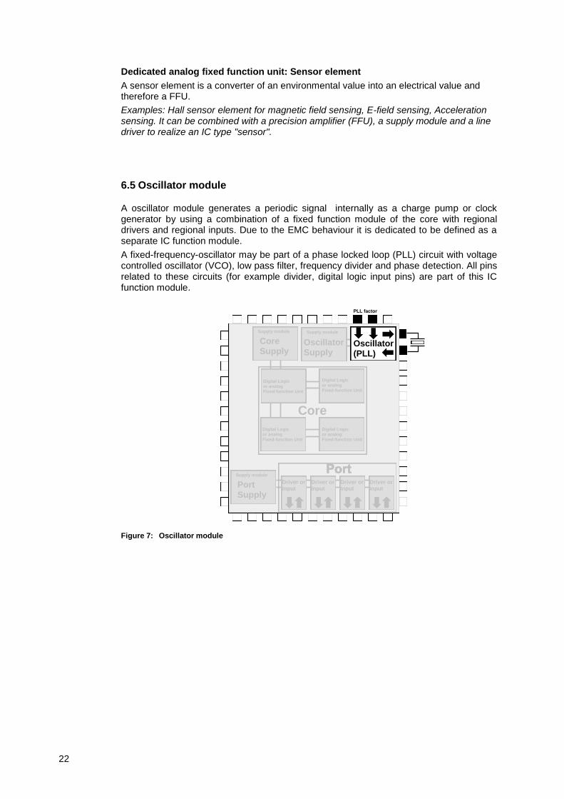
6.5 Oscillator module
A oscillator module generates a periodic signal internally as a charge pump or clock generator by using a combination of a fixed function module of the core with regional drivers and regional inputs. Due to the EMC behaviour it is dedicated to be defined as a separate IC function module.
A fixed-frequency-oscillator may be part of a phase locked loop (PLL) circuit with voltage controlled oscillator (VCO), low pass filter, frequency divider and phase detection. All pins related to these circuits (for example divider, digital logic input pins) are part of this IC function module.
Supply module
CoreSupply
Core
Supply module
PortSupply
Driver orInput
Driver orInput
Driver orInput
Driver orInput
Digital Logicor analogFixed-function Unit
Digital Logicor analogFixed-function Unit
Digital Logicor analogFixed-function Unit
Digital Logicor analogFixed-function Unit
Oscillator(PLL)
Supply module
OscillatorSupply
PLL factor
Figure 7: Oscillator module
23
6.6 Splitting ICs into IC function modules
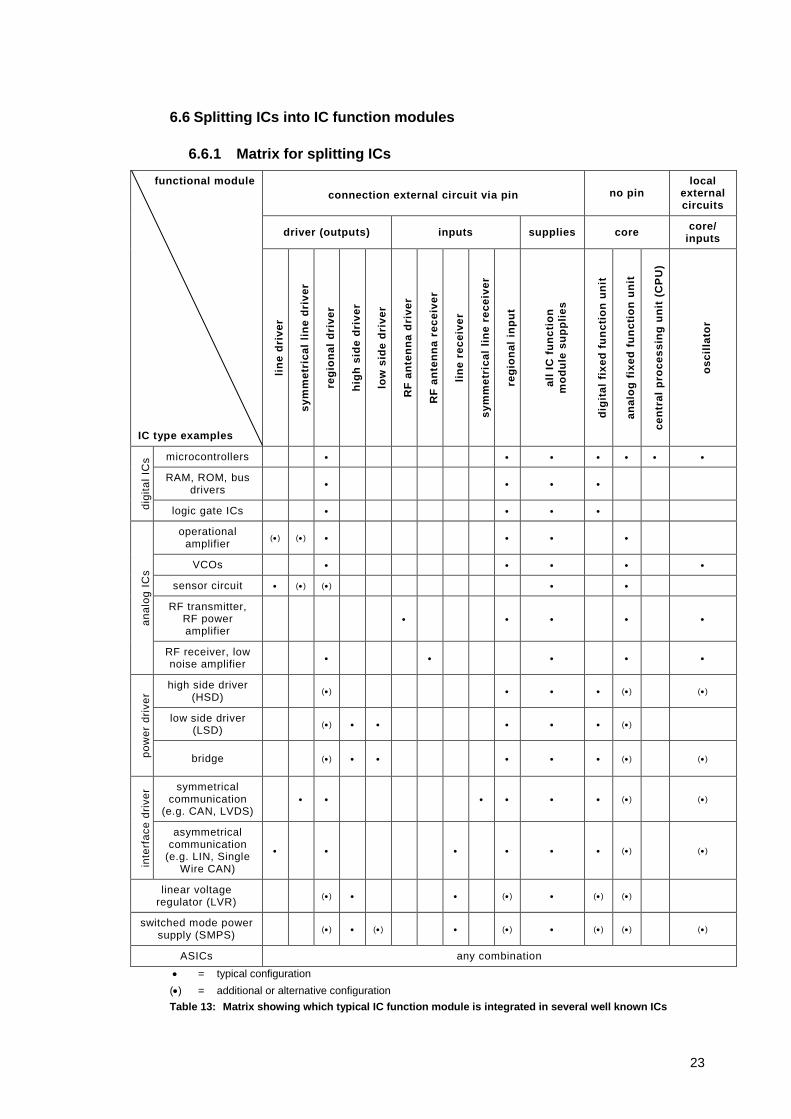
6.6.1 Matrix for splitting ICs
functional module
IC type examples
connection external circuit via pin no pin local
external circuits
driver (outputs) inputs supplies core core/
inputs
lin
e d
riv
er
sy
mm
etr
ica
l li
ne
dri
ve
r
reg
ion
al
dri
ve
r
hig
h s
ide
dri
ve
r
low
sid
e d
riv
er
RF
an
ten
na
dri
ve
r
RF
an
ten
na
re
ce
ive
r
lin
e r
ec
eiv
er
sy
mm
etr
ica
l li
ne
re
ce
ive
r
reg
ion
al
inp
ut
all
IC
fu
nc
tio
n
mo
du
le s
up
pli
es
dig
ita
l fi
xe
d f
un
cti
on
un
it
an
alo
g f
ixe
d f
un
cti
on
un
it
ce
ntr
al
pro
ce
ss
ing
un
it (
CP
U)
os
cil
lato
r
dig
ita
l IC
s microcontrollers
RAM, ROM, bus drivers
logic gate ICs
an
alo
g I
Cs
operational amplifier
() ()
VCOs
sensor circuit () ()
RF transmitter, RF power amplifier
RF receiver, low noise amplifier
po
we
r d
rive
r
high side driver (HSD)
() () ()
low side driver (LSD)
() ()
bridge () () ()
inte
rfa
ce
dri
ve
r symmetrical communication
(e.g. CAN, LVDS)
() ()
asymmetrical communication
(e.g. LIN, Single Wire CAN)
() ()
linear voltage regulator (LVR)
() () () ()
switched mode power supply (SMPS)
() () () () () ()
ASICs any combination
= typical configuration
() = additional or alternative configuration
Table 13: Matrix showing which typical IC function module is integrated in several well known ICs
24
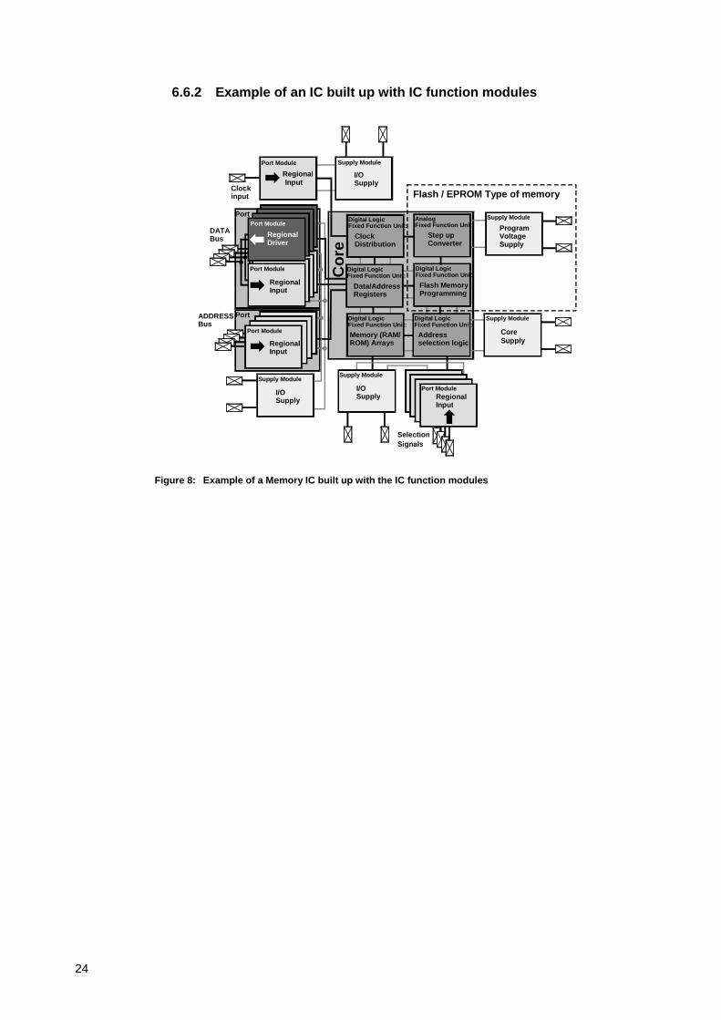
6.6.2 Example of an IC built up with IC function modules
Figure 8: Example of a Memory IC built up with the IC function modules
Co
re
Supply Module I/O Supply
Supply Module I/O Supply
Data/Address Registers
Digital Logic Fixed Function Unit:
Clock Distribution
DATA Bus
ADDRESS Bus
Supply Module I/O Supply
Selection Signals
Clock input
Address selection logic
Supply Module Program Voltage Supply
Analog Fixed Function Unit:
Step up Converter
Supply Module Core Supply
Flash Memory Programming
Flash / EPROM Type of memory
Memory (RAM/ ROM) Arrays
Regional Input
Digital Logic Fixed Function Unit:
Digital Logic Fixed Function Unit:
Digital Logic Fixed Function Unit:
Digital Logic Fixed Function Unit:
Port Module
Regional Input
Port Module
Regional Driver
Port Module
Regional Input
Port Module
Port
Port
Regional Input
Port Module
25
7 Selection guide for test configuration
7.1 Conducted tests
The test and measurement selection guide for conducted tests describes typical selection criteria for the coupling and injection points. It defines configurations and operating functions to characterize the EMC behaviour of the IC at relevant pins. The pin selection, configuration and function should be based on a typical application of the IC.
7.1.1 Pin selection for conducted RF emission and RF immunity tests
Port modules
All global pins shall be measured.
At a global driver pin the emission and immunity of the direct pin function, the crosstalk behaviour pin to core and the crosstalk behaviour port to pin can be detected.
At a global receiver pin only the crosstalk core to pin and port to pin can be detected.
If an IC has a high number of pins with the same specified functionality, it is not mandatory to measure all pins of such a functional group when a worst case assessment with respect to emission and immunity of the design has been performed and the selection is documented.
Local pin measurements are not mandatory.
Local pin measurements are optional and should be performed only on special request.
Supply modules
All supply pins shall be measured.
Core modules
The core can be measured indirectly only by crosstalk at global or local pins.
Oscillator modules
The emission of the oscillator should be measured only by crosstalk at global or local pins.
Immunity measurements can be performed optionally at the oscillator pins.
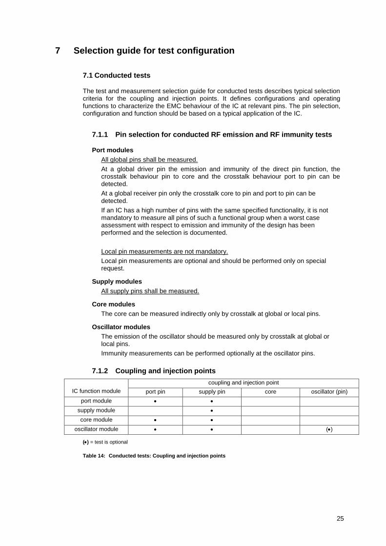
7.1.2 Coupling and injection points
IC function module
coupling and injection point
port pin supply pin core oscillator (pin)
port module
supply module
core module
oscillator module ()
() = test is optional
Table 14: Conducted tests: Coupling and injection points

26
7.1.3 Configuration for conducted RF emission tests
The following table provides necessary details to apply the selection part of the workflow for a dedicated IC. It starts with the selection of function modules with the related pin types, defines the measurement networks to be connected and it shows the operation modes and the expected coupling mechanisms in order to select the correct functional configuration and software if necessary.
coupling point
coupling mechanism functional configuration
direct indirect without CPU
(see chapter 10.1)
with CPU
(see chapter 10.2)
IC f
unctio
n m
odule
pin
type
measure
me
nt
netw
ork
(see c
hapte
r 8)
opera
tio
n m
ode *
)
functio
nal sig
nal
cro
ssta
lk c
ore
m
odule
to
cro
ssta
lk p
ort
mo
dule
to
cro
ssta
lk o
scill
ato
r
mo
dule
to
port
mo
dule
core
mo
dule
oscill
ato
r m
odule
port
mo
dule
core
mo
dule
oscill
ato
r m
odule
line driver global 8.1.1.1
T PM1 C1-S3
H CM1 C4-S2
H OM1 C6-S0
line receiver global 8.1.1.2 IA () CM1 C4-S2
sym. line driver
global 8.1.1.3
T PM3 C1-S3
IA CM1 C4-S2
IA OM1 C6-S0
sym. line receiver
global 8.1.1.4 IA () CM1 C4-S2
regional driver
local
8.1.1.5
config. A T PM5 C1-S3
H, L
CM1 C4-S2
H, L
OM1 C6-S0
8.1.1.5
config. B
H, L
PM5 C1-S2 C1-S3
regional Input
local 8.1.1.6 IA () CM1 C4-S2
high side driver
local, global
8.1.1.7
T PM7 C1-S3
H CM1 C4-S2
H OM1 C6-S0
low side driver
local, global
8.1.1.8
T PM8 C1-S3
H CM1 C4-S2
H OM1 C6-S0
RF antenna driver
see Annex B
RF antenna receiver
see Annex B
supply local, global
8.1.2
H SM1 C1-S3
H CM1 C4-S2
H OM1 C6-S0
() = test is optional
Table 15: Selection guide conducted RF emission
*) Note: T = toggle; H = static high potential, L = static low potential IA = defined inactive, realized with internal or external pull up or pull down

27
7.1.4 Configuration for conducted RF immunity tests
The following table provides the necessary details to apply the selection part of the workflow for a dedicated IC. It starts with the selection of function modules with the related pin types, defines the measurement networks to be connected and it shows the operation modes in order to select the correct functional configuration and the software if necessary.
injection point
functional configuration
without CPU (see chapter 10.1)
with CPU (see
chapter 10.2)
IC f
un
ctio
n
mo
dule
pin
typ
e
test n
etw
ork
(se
e c
hap
ter
8)
op
era
tio
n m
ode
*)
po
rt m
od
ule
co
re m
odu
le
oscill
ato
r m
odu
le
po
rt-,
co
re-,
oscill
ato
r m
odu
les
line driver global 8.1.1.1
T PM9 CM2 OM2 C10-S3
H PM9 CM2 OM2 C10-S3
IA CM3
line receiver global 8.1.1.2 A PM10 CM2 OM2 C10-S3
IA CM3
sym. line driver global 8.1.1.3
T PM11 CM2 OM2 C10-S3
IA PM11 CM2 OM2 C10-S3
IA CM3
sym. line receiver global 8.1.1.4 A PM12 CM2 OM2 C10-S3
IA CM3
regional driver local 8.1.1.5
config. A
T PM13 CM2 OM2 C10-S3
(H) PM13 CM2 OM2 C10-S3
(L) PM13 CM2 OM2
IA CM3
regional input local 8.1.1.6 A PM14 CM2 OM2 C10-S3
IA CM3
high side driver local, global
8.1.1.7
T PM15 CM2 OM2 C10-S3
(H) PM15 CM2 OM2 C10-S3
(L) PM15 CM2 OM2 C10-S3
IA CM3
low side driver local, global
8.1.1.8
T PM16 CM2 OM2 C10-S3
(H) PM16 CM2 OM2 C10-S3
(L) PM16 CM2 OM2 C10-S3
IA CM3
RF antenna driver see Annex B
RF antenna receiver see Annex B
supply local, global
8.1.2 H SM2 CM2 OM2 C10-S3
H SM2 CM3 OM2 C10-S3
oscillator local 8.1.4 T PM9 CM2 OM2 C10-S3
(operation mode) = test is optional
Table 16: Selection guide conducted RF immunity
*) Note: T = toggle; H = static high potential, L = static low potential A = defined active; IA = defined inactive, realized with internal or external pull up or pull down

28
7.1.5 Pin selection for conducted transient pulse immunity tests
If an IC function module has a related pin it has to be checked if this pin belongs to a transient exposure category according to Table 17.
transient exposure pin category
coupling of transient disturbances EMC pin type
1 pin directly connected to vehicle battery supply lines
global
2 pin directly connected to wiring harness
3 pin indirectly connected to vehicle battery supply lines (via loads, expected but not mandatory specified filter or protection devices)
4 pin indirectly connected to wiring harness I/O lines (via loads, expected but not mandatory specified filter or protection devices)
5 pin not directly connected to vehicle wiring harness (only relevant for cross coupling on PCB, coupling networks must be adapted)
local
Table 17: Pulse affected pins according to IEC62215-3
IC function modules might be assigned to different transient exposure pin categories. For a dedicated IC only one category shall be selected for testing.
IC function module configuration
transient exposure pin category
1 2 3 4 5
line driver single, multi - -
line receiver single, multi - -
sym. line driver - - -
sym. line receiver - - -
regional driver single, multi - - - - ()
regional input single, multi - - - - ()
high side driver
HSD*) - () - - -
LVR - - - () -
SMPS - - - () -
low side driver LSD - () - -
SMPS - - - -
RF antenna driver - - - - -
RF antenna receiver - - - - -
supply -
core - - - - -
oscillator - - - - ()
() = means to be tested optionally
*) HSD input directly tested via supply
Table 18: IC function module to transient exposure pin category matrix
29
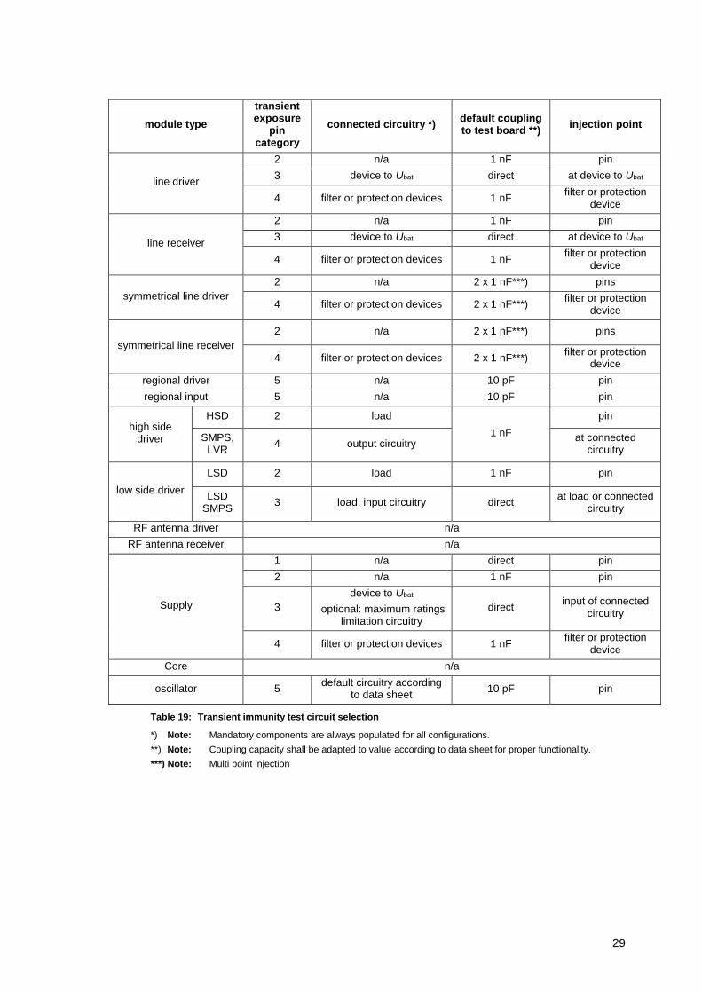
module type
transient exposure
pin category
connected circuitry *) default coupling to test board **)
injection point
line driver
2 n/a 1 nF pin
3 device to Ubat direct at device to Ubat
4 filter or protection devices 1 nF filter or protection
device
line receiver
2 n/a 1 nF pin
3 device to Ubat direct at device to Ubat
4 filter or protection devices 1 nF filter or protection
device
symmetrical line driver
2 n/a 2 x 1 nF***) pins
4 filter or protection devices 2 x 1 nF***) filter or protection
device
symmetrical line receiver
2 n/a 2 x 1 nF***) pins
4 filter or protection devices 2 x 1 nF***) filter or protection
device
regional driver 5 n/a 10 pF pin
regional input 5 n/a 10 pF pin
high side driver
HSD 2 load
1 nF
pin
SMPS, LVR
4 output circuitry at connected
circuitry
low side driver
LSD 2 load 1 nF pin
LSD SMPS
3 load, input circuitry direct at load or connected
circuitry
RF antenna driver n/a
RF antenna receiver n/a
Supply
1 n/a direct pin
2 n/a 1 nF pin
3
device to Ubat
optional: maximum ratings limitation circuitry
direct input of connected
circuitry
4 filter or protection devices 1 nF filter or protection
device
Core n/a
oscillator 5 default circuitry according
to data sheet 10 pF pin
Table 19: Transient immunity test circuit selection
*) Note: Mandatory components are always populated for all configurations.
**) Note: Coupling capacity shall be adapted to value according to data sheet for proper functionality.
***) Note: Multi point injection

30
7.1.6 Configuration for conducted transient pulse immunity tests
The following table provides the necessary details to apply the selection part of the workflow for a dedicated IC. It starts with the selection of function modules with the related pin types, defines the measurement networks to be connected and it shows the operation modes in order to select the correct functional configuration and the software if necessary.
injection point
functional configuration
without CPU (see chapter 10.1)
with CPU (see
chapter 10.2)
IC f
un
ctio
n
mo
dule
pin
typ
e
test
ne
two
rk
(se
e
ch
apte
r 8
)
op
era
tio
n
mo
de
*)
po
rt
mo
dule
co
re
mo
dule
oscill
ato
r
mo
dule
po
rt-,
co
re-
, o
scill
ato
r
mo
dule
s
line driver global 8.1.1.1
T PM9 CM2 OM2 C10-S3
H PM9 CM2 OM2 C10-S3
IA CM3
line receiver global 8.1.1.2 A PM10 CM2 OM2 C10-S3
IA CM3
sym. line driver global 8.1.1.3
T PM11 CM2 OM2 C10-S3
IA PM11 CM2 OM2 C10-S3
IA CM3
sym. line receiver global 8.1.1.4 A PM12 CM2 OM2 C10-S3
IA CM3
regional driver local 8.1.1.5
config. A
T PM13 CM2 OM2 C10-S3
(H) PM13 CM2 OM2 C10-S3
(L) PM13 CM2 OM2
IA CM3
regional input local 8.1.1.6 A PM14 CM2 OM2 C10-S3
IA CM3
high side driver local, global
8.1.1.7
T PM15 CM2 OM2 C10-S3
(H) PM15 CM2 OM2 C10-S3
(L) PM15 CM2 OM2 C10-S3
IA CM3
low side driver local, global
8.1.1.8
T PM16 CM2 OM2 C10-S3
(H) PM16 CM2 OM2 C10-S3
(L) PM16 CM2 OM2 C10-S3
IA CM3
RF antenna driver Annex B
RF antenna receiver Annex B
supply sub net
local, global
8.1.2 H SM2 CM2 OM2 C10-S3
H SM2 CM3 OM2 C10-S3
power net global 8.1.2 H SM2 CM2 OM2 C10-S3
oscillator local 8.1.4 T PM9 CM2 OM2 C10-S3
(operation mode) = test is optional
Table 20: Selection guide conducted transient immunity
*) Note: T = toggle; H = static high potential, L = static low potential A = defined active; IA = defined inactive, realized with internal or external pull up or pull down

31
7.1.7 Pin selection for unpowered system level ESD tests
The purpose of system level ESD packaging and handling test is to characterize protection capability for global pins of integrated circuits including mandatory components.
All global pins shall be tested according to the IC or customer specification vs. GND only.
IC level ESD packaging and handling tests on all pins (global and local) shall guarantee sufficient protection capability for safe and proper handling of semiconductor components (IC- manufacturing, - transport, - assembly on PCB). These tests and requirements are described in [15, 16, 17, 18]. They are part of the IC specification according to AECQ100 and therefore not considered in this specification.
7.1.8 Configuration for unpowered system level ESD tests
For unpowered system level ESD tests on IC pins an IC test configuration is not necessary.
7.2 Radiated tests
7.2.1 Criteria for performing radiated emission and immunity tests
Emission:
- the IC has a CPU, or
- the IC has a digital logic FFU or an oscillator module with an operating frequency higher than 10 MHz and a package diagonal dimension greater than 25 mm
Immunity:
- the IC has an analog FFU as sensing element working with electrical or magnetic fields, or
- the IC has an analog or digital FFU with charge coupled devices (CCD) for filtering
7.2.2 Test configuration for radiated emission
Table 21: Selection guide radiated emission
7.2.3 Test configuration for radiated immunity
injection structure test setup functional configuration
entire IC
(G)TEM-cell chapter 9.2 or
IC stripline chapter 9.3
without CPU with CPU
CM2 C10-S3
CM3 C11-S3
Table 22: Selection guide radiated immunity
coupling structure test setup functional configuration
entire IC
(G)TEM-cell chapter 9.2 or
IC stripline chapter 9.3
without CPU with CPU
CM1 C1-S2

32
8 Test and measurement networks
8.1 Emission and immunity tests
This chapter describes the coupling, injection and monitoring networks for conducted emission measurements and immunity tests. All unused pins shall be set into a defined state and configuration according to the IC data sheet. The electrical characteristics (power dissipation, voltage, current, frequency properties) of the passive components on the test PCB shall meet the functional and test requirements.
The trace impedance between the RF connector and coupling network and to the pin under test shall be 50 Ω.
8.1.1 Port module
8.1.1.1 Line driver
For common line drivers the following networks shall be used, for special line drivers type LIN refer to specification [20].
IC
lin
e d
river
core
R2
C1
R1
Ztrace = 50 Ω
configuration A: single line driver port
ICli
ne
dri
ver
core
RA1
R2
Ztrace = 50 Ω
CB1
RA2
RAn
CB2
CBn
configuration B: common mode network *)
Figure 9: Test and measurement networks for line driver
*) Note: Use circuit B for common mode testing only (e.g. airbag squib driver, sensors, application acc. to Annex F of IEC 61967-4)
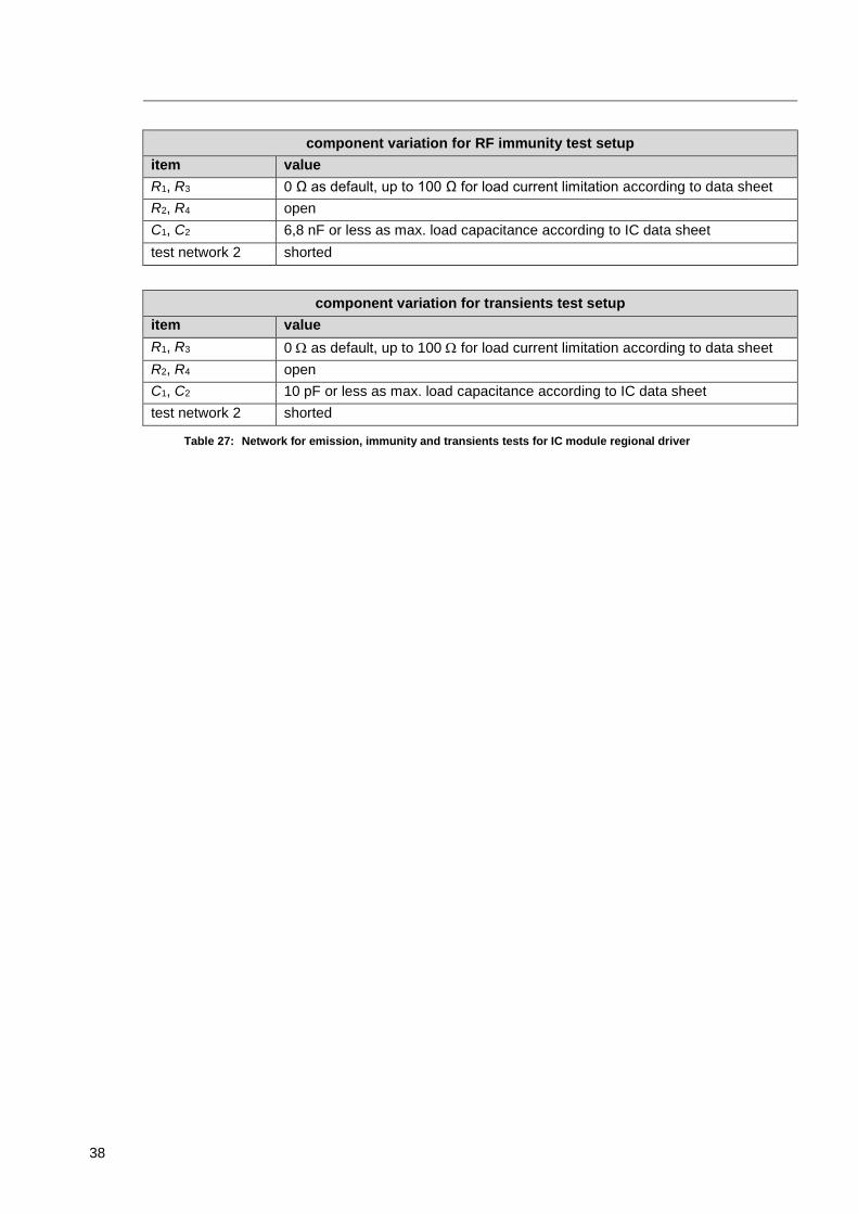
component variation for RF emission test setup
item value
R1 120 Ω
R2 51 Ω
C1 6.8 nF or less as max. load capacitance according to IC data sheet
RA1= RA2=...=RAn nR 120%5A n = number of Line Drivers
select a resistor according to resistor standard set within tolerance of 5%
CB1= CB2=...= CBn n
CC 1
%5B n = number of Line Drivers
Select a capacitor according to capacitor standard set within tolerance of 5%
33
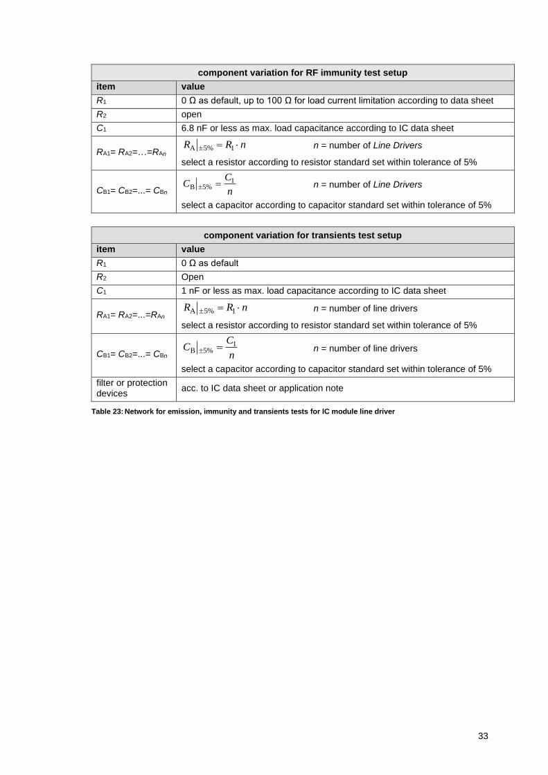
component variation for RF immunity test setup
item value
R1 0 Ω as default, up to 100 Ω for load current limitation according to data sheet
R2 open
C1 6.8 nF or less as max. load capacitance according to IC data sheet
RA1= RA2=…=RAn nRR 1%5A n = number of Line Drivers
select a resistor according to resistor standard set within tolerance of 5%
CB1= CB2=...= CBn n
CC 1
%5B n = number of Line Drivers
select a capacitor according to capacitor standard set within tolerance of 5%
component variation for transients test setup
item value
R1 0 Ω as default
R2 Open
C1 1 nF or less as max. load capacitance according to IC data sheet
RA1= RA2=...=RAn nRR 1%5A n = number of line drivers
select a resistor according to resistor standard set within tolerance of 5%
CB1= CB2=...= CBn n
CC 1
%5B n = number of line drivers
select a capacitor according to capacitor standard set within tolerance of 5%
filter or protection devices
acc. to IC data sheet or application note
Table 23: Network for emission, immunity and transients tests for IC module line driver
34
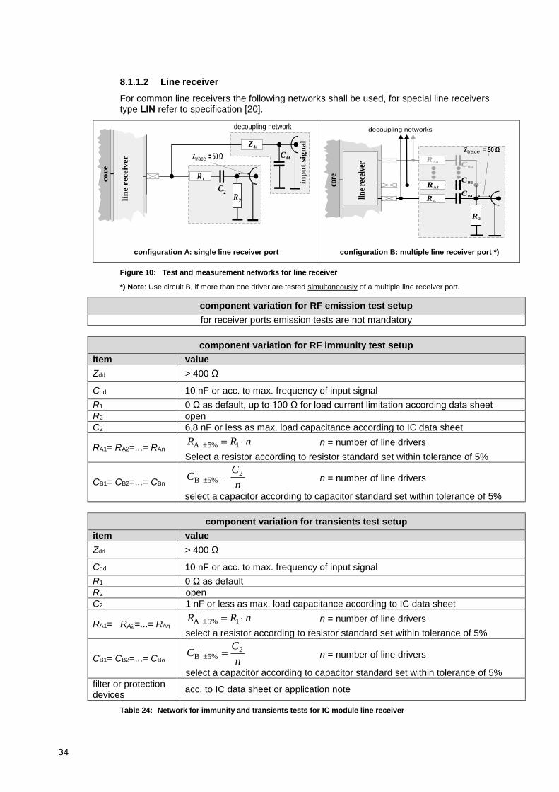
8.1.1.2 Line receiver
For common line receivers the following networks shall be used, for special line receivers type LIN refer to specification [20].
IC
core
Cdd
lin
e r
eceiv
er
Zdd
R1
R2
C2
in
pu
t sig
nal
decoupling network
Ztrace = 50 Ω
configuration A: single line receiver port
IC
lin
e re
ceiv
er
core
RA1
R2
CB1
RA2
RAn
CB2
CBn
Ztrace = 50 Ω
decoupling networks
configuration B: multiple line receiver port *)
Figure 10: Test and measurement networks for line receiver
*) Note: Use circuit B, if more than one driver are tested simultaneously of a multiple line receiver port.
component variation for RF emission test setup
for receiver ports emission tests are not mandatory
component variation for RF immunity test setup
item value
Zdd > 400 Ω
Cdd 10 nF or acc. to max. frequency of input signal
R1 0 Ω as default, up to 100 Ω for load current limitation according data sheet
R2 open
C2 6,8 nF or less as max. load capacitance according to IC data sheet
RA1= RA2=...= RAn nRR 1%5A n = number of line drivers
Select a resistor according to resistor standard set within tolerance of 5%
CB1= CB2=...= CBn n
CC 2
%5B n = number of line drivers
select a capacitor according to capacitor standard set within tolerance of 5%
component variation for transients test setup
item value
Zdd > 400 Ω
Cdd 10 nF or acc. to max. frequency of input signal
R1 0 Ω as default
R2 open
C2 1 nF or less as max. load capacitance according to IC data sheet
RA1= RA2=...= RAn nRR 1%5A n = number of line drivers
select a resistor according to resistor standard set within tolerance of 5%
CB1= CB2=...= CBn n
CC 2
%5B n = number of line drivers
select a capacitor according to capacitor standard set within tolerance of 5%
filter or protection devices
acc. to IC data sheet or application note
Table 24: Network for immunity and transients tests for IC module line receiver

35
8.1.1.3 Symmetrical line driver
For common symmetrical line drivers the following networks shall be used, for special symmetrical line drivers type CAN refer to specification [19].
Figure 11: Test and measurement networks for symmetrical line driver
component variation for RF emission test setup
item value
RB according to bus specification*)
RA 240 Note: the resistors shall be matched with tolerance better than 0.1%
R2 51
CB
6,8 nF or max. load capacitance according to IC data sheet Note: the capacitors shall be matched with tolerance better than 1%
component variation for RF immunity test setup
item value
RB according to bus specification*)
RA 0 as default, up to 100 for load current limitation according to data sheet Note: the resistors shall be matched with tolerance better than 0.1%
R2 open
CB 6,8 nF or less as max. load capacitance according to IC data sheet Note: the capacitors shall be matched with tolerance better than 1%
component variation for transients test setup
item value
RB according to bus specification*)
RA 0 as default
R2 open
CB 1 nF (or less as max. load capacitance according to data sheet) Note: the capacitors shall be matched with tolerance better than 1%
filter or protection devices
acc. to IC data sheet or application note
Table 25: Network for emission, immunity and transients tests for IC module symmetrical line driver
*) Note: Termination is not part of the test network, but may be needed for the symmetrical line driver
sym
met
rica
l
lin
e d
riv
er
core
CB
CB
RA
RA
RB
2
Ztrace = 50 Ω
R

36
8.1.1.4 Symmetrical line receiver
For common symmetrical line drivers the following networks shall be used, for special symmetrical line receivers type CAN refer to specification [19].
IC
sym
met
rica
l
lin
e re
ceiv
er
core
CB
CB
RA
RA
RB
2
Ztrace = 50 Ω
R
Figure 12: Test and measurement networks for symmetrical line receiver
component variation for RF emission test setup
for symmetrical line receiver ports emission tests are not mandatory
component variation for RF immunity test setup
item value
RB according to bus specification*)
RA 0 as default, up to 100 for load current limitation according to data sheet Note: the resistors shall be matched with tolerance better than 0,1%
R2 open
CB 6,8 nF or less as max. load capacitance according to IC data sheet Note: the capacitors shall be matched with tolerance better than 1%
component variation for transients test setup
item value
RB according to bus specification*)
RA 0 as default, up to 100 for load current limitation according to data sheet Note: the resistors shall be matched with tolerance better than 0,1%
R2 open
CB 1 nF (or less as max. load capacitance according to data sheet) Note: the capacitors shall be matched with tolerance better than 1%
filter or protection devices
acc. to IC data sheet or application note
Table 26: Network for immunity and transients tests for IC module symmetrical line receiver
*) Note: Termination is not part of the test network, but may be needed for the symmetrical line receiver
37
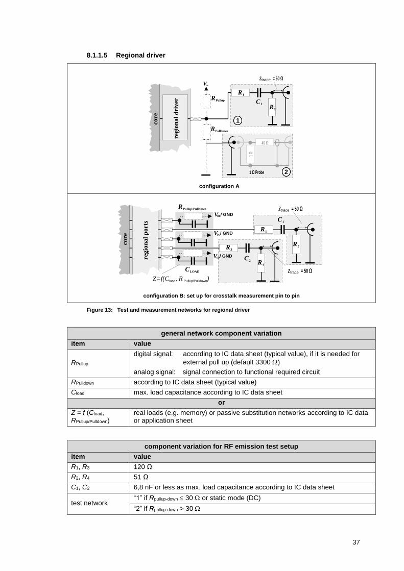
8.1.1.5 Regional driver
core
R1
R2
C1
Vcc
RPullup
2
49 Ω
1
RPulldown
reg
ion
al
dri
ver
Ztrace = 50 Ω
1 Ω
1 Ω Probe
configuration A
IC
core
R1
R2
C1
CLOAD
RPullup/Pulldown
V / GNDDD
R3
R4
reg
ion
al
port
s
C2
V / GNDDD
V / GNDDD
Z=f(C , R )load Pullup/Pulldown
Ztrace = 50 Ω
Ztrace = 50 Ω
configuration B: set up for crosstalk measurement pin to pin
Figure 13: Test and measurement networks for regional driver
general network component variation
item value
RPullup
digital signal: according to IC data sheet (typical value), if it is needed for
external pull up (default 3300 )
analog signal: signal connection to functional required circuit
RPulldown according to IC data sheet (typical value)
Cload max. load capacitance according to IC data sheet
or
Z = f (Cload, RPullup/Pulldown)
real loads (e.g. memory) or passive substitution networks according to IC data or application sheet
component variation for RF emission test setup
item value
R1, R3 120 Ω
R2, R4 51 Ω
C1, C2 6,8 nF or less as max. load capacitance according to IC data sheet
test network “1” if Rpullup-down 30 or static mode (DC)
“2” if Rpullup-down > 30
38
component variation for RF immunity test setup
item value
R1, R3 0 Ω as default, up to 100 Ω for load current limitation according to data sheet
R2, R4 open
C1, C2 6,8 nF or less as max. load capacitance according to IC data sheet
test network 2 shorted
component variation for transients test setup
item value
R1, R3 0 as default, up to 100 for load current limitation according to data sheet
R2, R4 open
C1, C2 10 pF or less as max. load capacitance according to IC data sheet
test network 2 shorted
Table 27: Network for emission, immunity and transients tests for IC module regional driver

39
8.1.1.6 Regional input
IC
core
Cdd
reg
ion
al
inp
ut
Zdd
R2
C2
in
pu
t si
gn
al
decoupling network
Ztrace = 50 Ω
R1
Figure 14: Test and measurement networks for regional input
component variation for RF emission test setup
for input ports emission tests are not mandatory
component variation for RF immunity test setup
item value
Zdd > 400 Ω
Cdd 10 nF or acc. to max. frequency of input signal
R1 0 Ω as default, up to 100 Ω for load current limitation according to data sheet
R2 open
C2 6,8 nF or less as max. load capacitance according to IC data sheet)
component variation for transients test setup
item value
Zdd > 400 Ω
Cdd 10 nF or acc. to max. frequency of input signal
R1 0 as default, up to 100 for load current limitation according to data sheet
R2 open
C2 10 pF(or less as max. load capacitance according to IC data sheet)
Table 28: Network for immunity and transients tests for IC module regional input
40
8.1.1.7 High side driver
Emission: In addition to IEC61967-4, the impedance determining 150 network and the load impedance are decoupled by a 5 µH coil (LBAN), to get results independent from the load impedance.
Immunity: In addition to IEC62132-4, a broadband artificial network (BAN) consisting
of a 5 µH coil (LBAN) and a 150 matching network (RBAN , CBAN) for impedance fixing is added.
reference
outputIC
hig
h s
ide
dri
ver
core
R1
R2
C 1
LBAN
C2
RLoad
supply
1
RBAN
CBAN
Ztrace = 50 ΩZtrace = 50 Ω
decoupling
network
21 Ω Probe
1 Ω
49 Ω
configuration high side driver
reference
outputIC
hig
h s
ide
dri
ver
core
R1
R2
C 1
LBAN
C2
RLoad
D1
supply
1L1
RBAN
CBAN
Ztrace = 50 ΩZtrace = 50 Ω
decoupling
network
configuration switched mode power supply / linear voltage regulator
Figure 15: Test and measurement networks for high side driver

41
general network component variation
item value for high side driver
value for linear voltage regulator
value for switched mode power supply (buck converter)
LBAN 5 µH (independent of load current, no saturation effects, ZLBAN (5-1000MHz) ≥ 150 )
L1 shorted shorted acc. to IC data sheet
D1 open open acc. to IC data sheet
C2 open acc. to IC data sheet acc. to IC data sheet
Rload
according to Imeas*)
C150,onthmeas
RR
TI
(T = 65 K, Imeas 10 A)
according to Imeas*)
Imeas = 80 % of Inom
according to Imeas*)
Imeas = 80% of Inom
*) Note: The IC dissipation power Pdissipation is basically limited by Rth of the housing and the maximum temperature Tmax of the semiconductor at a maximum ambient temperature Tamb according to data
sheet. With the definitions Tmax = 150°C at Tamb = 85°C a T = 65K is given. The typical power
dissipation is additionally given by Ron,150*C and a typical load current Iload: CRIP 150,on2
oadlndissipatio
and thndissipatio RPT .
component variation for RF emission test setup
item value for high side driver
value for linear voltage regulator
value for switched mode power supply (buck converter)
R1 120 120 120
R2 51 51 51
C1 6,8 nF 6,8 nF 6,8 nF
test network 1
Rload 30 or static mode (DC)
Rload 30 or static mode (DC)
Rload 30 or static mode (DC)
test network 2
Rload > 30 ,
LBAN short n/a n/a
RBAN open open open
CBAN open open open
component variation for RF immunity test setup
item value for high side driver
value for linear voltage regulator
value for switched mode power supply (buck converter)
R1 0 as default, up to 100 for load current limitation according to data sheet
R2 open open open
C1 6,8 nF or less as max. load capacitance according to IC data sheet
RBAN 150 150 150
CBAN 6,8 nF 6,8 nF 6,8 nF
42
component variation for transients test setup
item value for high side
driver value for linear voltage
regulator
value for switched mode power supply (buck
converter)
R1 0 as default, up to 100 for load current limitation according to data sheet
R2 open open open
C1 global pin: 1 nF (or less as max. load capacitance according to IC data sheet)
local pin: 10 pF(or less as max. load capacitance according to IC data sheet)
RBAN 150 150 150
CBAN 6,8 nF 6,8 nF 6,8 nF
Table 29: Network for emission, immunity and transients tests for IC module high side driver
8.1.1.8 Low side driver
Emission: In addition to IEC61967-4, the impedance determining 150 network and the load impedance are decoupled by a 5 µH coil (LBAN), to get results independent from the load impedance.
Immunity: In addition to IEC62132-4, a broadband artificial network (BAN) consisting
of a 5 µH coil (LBAN) and a 150 matching network (RBAN , CBAN) for impedance fixing is added.

43
output l
ow
sid
e
dri
ver
core
R2
C1
supply
2
1
reference
RLoad,1
VSupply
LBAN1
RBAN1
CBAN1
R1
Ztrace = 50 ΩZtrace = 50 Ω
1 Ω Probe
1 Ω
49 Ω
decoupling
network
configuration low side driver
outputIC
lo
w s
ide
dri
ver
core
R3
R4
C2
supply
1reference
L1
D1
C4
RLoad,2
VSupply
LBAN1
C3
LBAN2
RBAN2
CBAN2
RBAN1
CBAN1
R1
R2
C1
1
Ztrace = 50 Ω Ztrace = 50 Ω
Ztrace = 50 Ω
configuration switched mode power supply
Figure 16: Test and measurement networks for low side driver

44
general network component variation
item value for low side driver value for switched mode power supply (boost converter)
L1 shorted acc. to IC data sheet
D1 shorted acc. to IC data sheet
C3 open acc. to IC data sheet
C4 open acc. to IC data sheet
Rload,1**)
according to Imeas*)
CRR
TI
150,onthmeas
(T = 65 K, Imeas 10 A)
n/a
Rload,2 n/a according to Imeas
Imeas = 80% of Inom
*) Note: The IC dissipation power Pdissipation is basically limited by Rth of the housing and the maximum temperature Tmax of the semiconductor at a maximum ambient temperature Tamb according to data
sheet. With the definitions Tmax = 150°C at Tamb = 85°C a T = 65K is given. The typical power
dissipation is additionally given by Ron,150*C and a typical load current Iload: CRIP 150,on2
oadlndissipatio
and thndissipatio RPT .
**) Note: If a specific load (e.g. solenoid) is defined and available it shall be used.
component variation for RF emission test setup
item value for low side driver value for switched mode power supply (boost converter)
LBAN1 5 µH (independent of load current, no saturation effects, ZLBAN (5-1000MHz) ≥ 150 )
LBAN2 shorted 5 µH
R1, R3 120 120
R2, R4 51 51
C1, C2 6,8 nF 6,8 nF
test network 1 Rload 30 or static mode (DC) Rload 30 or static mode (DC)
test network 2 Rload > 30 n/a
RBAN1, RBAN2 open open
CBAN1, CBAN2 open open
component variation for RF immunity test setup
item value for low side driver value for switched mode power supply (boost converter)
LBAN1 5 µH (independent of load current, no saturation effects, ZLBAN (5-1000MHz) ≥ 150 )
LBAN2 shorted 5 µH
R1, R3 0 as default, up to 100 for load current limitation according to data sheet
R2, R4 open open
C1, C2 6,8 nF or less as max. load capacitance according to IC data sheet
RBAN1, RBAN2 150 150
CBAN1, CBAN2 6,8 nF 6,8 nF
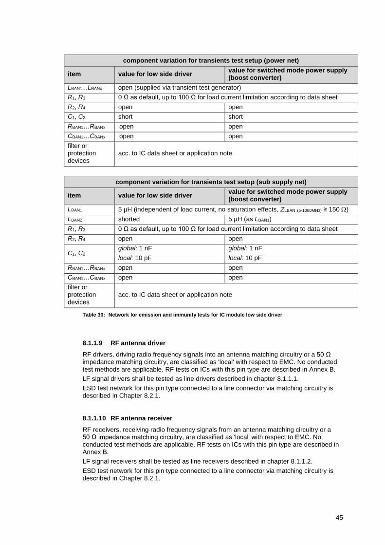
45
component variation for transients test setup (power net)
item value for low side driver value for switched mode power supply (boost converter)
LBAN1...LBANx open (supplied via transient test generator)
R1, R3 0 Ω as default, up to 100 Ω for load current limitation according to data sheet
R2, R4 open open
C1, C2 short short
RBAN1…RBANx open open
CBAN1…CBANx open open
filter or protection devices
acc. to IC data sheet or application note
component variation for transients test setup (sub supply net)
item value for low side driver value for switched mode power supply (boost converter)
LBAN1 5 µH (independent of load current, no saturation effects, ZLBAN (5-1000MHz) ≥ 150 )
LBAN2 shorted 5 µH (as LBAN1)
R1, R3 0 Ω as default, up to 100 Ω for load current limitation according to data sheet
R2, R4 open open
C1, C2 global: 1 nF global: 1 nF
local: 10 pF local: 10 pF
RBAN1…RBANx open open
CBAN1…CBANx open open
filter or protection devices
acc. to IC data sheet or application note
Table 30: Network for emission and immunity tests for IC module low side driver
8.1.1.9 RF antenna driver
RF drivers, driving radio frequency signals into an antenna matching circuitry or a 50 Ω impedance matching circuitry, are classified as 'local' with respect to EMC. No conducted test methods are applicable. RF tests on ICs with this pin type are described in Annex B.
LF signal drivers shall be tested as line drivers described in chapter 8.1.1.1.
ESD test network for this pin type connected to a line connector via matching circuitry is described in Chapter 8.2.1.
8.1.1.10 RF antenna receiver
RF receivers, receiving radio frequency signals from an antenna matching circuitry or a 50 Ω impedance matching circuitry, are classified as 'local' with respect to EMC. No conducted test methods are applicable. RF tests on ICs with this pin type are described in Annex B.
LF signal receivers shall be tested as line receivers described in chapter 8.1.1.2.
ESD test network for this pin type connected to a line connector via matching circuitry is described in Chapter 8.2.1.
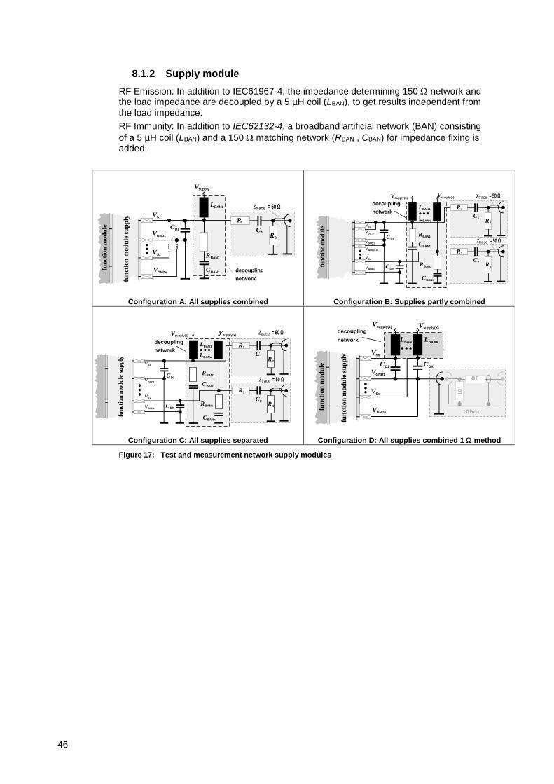
46
8.1.2 Supply module
RF Emission: In addition to IEC61967-4, the impedance determining 150 network and the load impedance are decoupled by a 5 µH coil (LBAN), to get results independent from the load impedance.
RF Immunity: In addition to IEC62132-4, a broadband artificial network (BAN) consisting
of a 5 µH coil (LBAN) and a 150 matching network (RBAN , CBAN) for impedance fixing is added.
decoupling
network
R1
R2
C1
fun
ctio
n m
od
ule
fun
ctio
n m
od
ule
su
pp
ly
VSx
VS1
VGND1
VGNDx
Vsupply
LBAN1
CD1
RBAN1
CBAN1
Ztrace = 50 Ω
Configuration A: All supplies combined
IC
fun
ctio
n m
od
ule
VSx
VS1
VGND1
VGNDx
Vsupply(x)Vsupply(1)
LBAN1
LBANx
CDX
CD1
C1
VGND2..n
VS2..n
C2
RBAN1
RBANx
CBAN1
CBANx
R3
R1
R2
R4
Ztrace = 50 Ω
Ztrace = 50 Ω
decoupling
network
Configuration B: Supplies partly combined
fun
ctio
n m
od
ule
su
pp
ly
VSx
VS1
VGND1
VGNDx
Vsupply(x)Vsupply(1)
LBAN1
LBANx
CDX
CD1
C1
C2
RBAN1
RBANx
CBAN1
CBANx
R3
R1
R2
R4
Ztrace = 50 Ω
decoupling
network
Ztrace = 50 Ω
Configuration C: All supplies separated
IC
fun
ctio
n m
od
ule
fun
ctio
n m
od
ule
su
pp
ly
VSx
VS1
VGND1
VGNDx
Vsupply(X)Vsupply(1)
LBAN1 LBANX
CDXCD1
decoupling
network
1 Ω Probe
1 Ω
49 Ω
Configuration D: All supplies combined 1 method
Figure 17: Test and measurement network supply modules
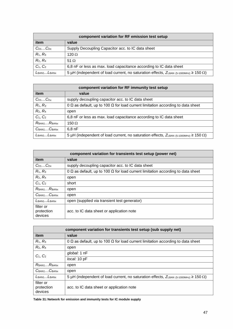
47
component variation for RF emission test setup
item value
CD1…CDx Supply Decoupling Capacitor acc. to IC data sheet
R1, R3 120
R2, R4 51
C1, C2 6,8 nF or less as max. load capacitance according to IC data sheet
LBAN1...LBANx 5 µH (independent of load current, no saturation effects, ZLBAN (5-1000MHz) ≥ 150 )
component variation for RF immunity test setup
item value
CD1…CDx supply decoupling capacitor acc. to IC data sheet
R1, R3 0 Ω as default, up to 100 Ω for load current limitation according to data sheet
R2, R4 open
C1, C2 6,8 nF or less as max. load capacitance according to IC data sheet
RBAN1…RBANx 150
CBAN1…CBANx 6,8 nF
LBAN1...LBANx 5 µH (independent of load current, no saturation effects, ZLBAN (5-1000MHz) ≥ 150 )
component variation for transients test setup (power net)
item value
CD1…CDx supply decoupling capacitor acc. to IC data sheet
R1, R3 0 Ω as default, up to 100 Ω for load current limitation according to data sheet
R2, R4 open
C1, C2 short
RBAN1…RBANx open
CBAN1…CBANx open
LBAN1...LBANx open (supplied via transient test generator)
filter or protection devices
acc. to IC data sheet or application note
component variation for transients test setup (sub supply net)
item value
R1, R3 0 Ω as default, up to 100 Ω for load current limitation according to data sheet
R2, R4 open
C1, C2 global: 1 nF
local: 10 pF
RBAN1…RBANx open
CBAN1…CBANx open
LBAN1...LBANx 5 µH (independent of load current, no saturation effects, ZLBAN (5-1000MHz) ≥ 150 )
filter or protection devices
acc. to IC data sheet or application note
Table 31: Network for emission and immunity tests for IC module supply

May 2017
German Electrical and Electronic Manufacturers´ Association
8.1.3 Core module
The conducted emission and immunity of the core module cannot be measured directly. All emission or immunity tests shall be performed by using cross talk effects between
core and supply
core and port
core and oscillator
8.1.4 Oscillator module
The emission of the oscillator should be measured only by crosstalk at global or local pins.
Immunity measurements can be performed optionally directly at the oscillator.
IC
osc
illa
tor
in
pu
t
ou
tpu
t
core
quartz
C2
(Ztrace = 50
C1
(Ztrace = 50
JMP1
JMP2
R1
R2
R3
R4
Figure 18: Test and measurement networks oscillator module
component variation for RF emission test setup
for oscillator modules emission tests are not required
component variation for RF immunity test setup
item value
R1, R2 0 Ω
C1, C2 oscillator capacitors: 10 pF or maximum according to data sheet
JMP1, JMP2 jump plug (R3=R4=50 ) connected to the not used injection point
component variation for transients test setup
item value
R1, R2 0 Ω
C1, C2 Oscillator capacitors: 10 pF or maximum according to data sheet
JMP1, JMP2 Jump plug (R3=R4=50 ) connected to the not used injection point
Table 32: Network for immunity tests for IC module oscillator

49
8.2 ESD test
8.2.1 Test network for unpowered system level ESD tests
ESD test on global pins shall be performed according to the following test network. All GND pins shall be shorted on the test board. All other pins can be left open.
mandatory
components
Vsupply
PUT
GNDGND
Vsupply
contact discharge point
CsRd Rp
Figure 19: Test network for unpowered system ESD test on global pin
ESD network for global supply pin
item value
Cs
capacitor for decoupling purpose
100 nF
if no other value is specified
Rd
discharge resistor parallel to decoupling capacitance Vsupply to GND for self-discharging after ESD test and avoids pre-charging of the pin under test by the ESD gun before testing (see Figure 19)
≥ 220 kΩ
mandatory components as specified acc. to data sheet
additional
external components
as described in application note, test specification, test report, etc.
Table 33: External components global supply pin
ESD network for global port pin
item value
Rp
discharge resistor parallel to pin under test to avoid pre-charging of the pin under test by the ESD gun before testing and to discharge the pin under test after ESD testing (see Figure 19)
≥ 220 kΩ
mandatory components as specified acc. to data sheet
additional external components as described in application note, test specification, test report, etc.
Table 34: External components global port pin

50
9 Test setup
9.1 Signal decoupling for stimulus and monitoring
9.1.1 Stimulus setup
The stimulus signals and setup should not affect the measurements. Following topics should be considered to reach this requirement:
The reference ground on PCB for functionality, RF and transient test signals should be checked and optimized for current separation.
For external clock injection coaxial cables with appropriate RF connector types, short traces to the clock input pin(s) and separate ground routing shall be used. The emission of the unpowered test board with active external clock has to be verified.
For emission measurements the signal-to-disturbance margin of the stimulus signal can be reduced to the minimum stimulus signal definition parameters: maximum rise and fall times, minimum signal amplitude, maximum source impedance.
9.1.2 DUT Monitoring
The pins to be monitored shall be specified in the dedicated IC EMC test specification.
Generally, all DUT functions, which are decided to be monitored, have to be checked. For conducted RF immunity and transient tests the DUT functions can be monitored directly or indirectly at output ports. For radiated immunity tests the distinction between direct and indirect monitoring is not possible. All monitored signals shall be within the failure criteria of the IC EMC test specification.
direct monitoring: Monitoring at the pin under test
indirect monitoring: All other monitoring
RF decoupling: RF filter necessary to prevent the monitoring device from the disturbance.
transients decoupling: Signal decoupling by fibre optic conversion might be necessary to prevent the monitoring device from the disturbance.
monitoring device: The monitoring can be realized e.g. by a microcontroller (µC) test application with a cycling test program, an oscilloscope with a programmable signal tolerance mask, a multimeter.
An example how the monitored signals can be combined to a logical sum "within specification or out of specification” is shown in Figure 20.
Figure 20: DUT monitoring
output signal
function
DUT
DUT within spec.
or
one or more functions out of spec.
failure criteria
indirect monitoring
direct monitoring
decoupling
decoupling
decoupling
monitoring device
pass
fail
pass
fail
pass
fail
disturbance injection
OR function
function
output signal
output signal

51
Failure criteria:
For monitored signals failure criteria have to be defined in the dedicated IC EMC test specification. A failure criterion is defined by its nominal signal values and allowed tolerances. An example of failure criteria for typical signals is shown in Table 35.
failure criterion no. monitored function failure criteria
1 analog output 2,5 V 0,2 V
2 'status' output digital signal '1'
n … …
Table 35: Example of a failure criteria table
Disturbance signatures superposed on the monitored signal are not regarded as failure caused by the IC under test and shall not be considered.
Activated protection or diagnosis functions (over voltage, under voltage, over current, etc.) or for example current variations caused by changing operation conditions during transient pulse injection test shall not be regarded as functional failure but have to be noted in the test report.
9.1.3 Monitoring setup
The signal decoupling- and monitoring setup with or without external filter elements should not affect functional signals and not significantly reduce injected disturbance signals. It is recommended that the filter impedance is higher than 400 Ω in the test frequency range. An example of filter definition is shown in Figure 21.
in-/outputIC
core
R1
supply
reference
C1
Ulowpass, outUlowpass,in
to load network /from signal source
to supply network
1
2
port
/Su
pp
ly/
osc
illa
tor
mod
ule
Configuration 1: Monitoring network at input or output
Configuration 2: Monitoring network supply
Figure 21: General setup for a decoupling network for monitoring
Basis of filter calculation:
transfer ratio: 11inlowpass,
outlowpass,
21
1
CRfjU
Ua
magnitude of the transfer ratio in dB
2
12
122
inlowpass,
outlowpass,
41
1log20
CRfU
Ua
Limit for the magnitude of the transfer ratio < -20 dB, requires R1 > 400 Ω in the test frequency range
Note: Reflection coefficient for R1 ≥ 400 Ω in a 50 Ω system ≥ 0,8

52
-100
-90
-80
-70
-60
-50
-40
-30
-20
-10
0
0,01 0,1 1 10 100 1000
frequency f / MHz
tra
ns
fer
rati
o /
dB
R=400Ohm, C=0.5nF
R=400Ohm, C=10nF
R=1kOhm, C=1nF
R=6.8kOhm, C=2nF
R=10kOhm, C=6.8nF
transfer function chart for examples for different
values of R1, C1
for direct and indirect monitoring
Figure 22: Decoupling network for monitoring: transfer functions for low pass circuitry examples
9.1.4 Performance classes for immunity testing
The FFU functional states are defined in [10].
performance class
definition
similar to
FPSC in ISO 11452-1
AIC all monitored functions of the IC perform within the defined tolerances during and after exposure to disturbance
I
BIC*) short time degradation of one or more monitored signals during exposure to disturbance is not evaluable for IC only. Therefore this classification may not be applicable for ICs
CIC at least one of the monitored functions of the IC is out of the defined tolerances during the disturbance but returns automatically to the defined tolerances after exposure to disturbance
II
D1IC, D2IC
at least one monitored function of the IC does not perform within the defined tolerances during exposure and does not return to normal operation by itself. The IC returns to normal operation by manual intervention
class D1: reset
class D2: power cycling
III
IV
EIC at least one monitored function of the IC does not perform within the defined tolerances after exposure and cannot be returned to proper operation
Table 36: Definition of performance classes
*) Note: Short time degradation of one or more monitored signals might be tolerable in the application by its error handling. This error handling is unknown in most cases for IC test.

53
9.2 (G)TEM-cell setup
The measurement of radiated electromagnetic fields with the (G)TEM cell and the immunity against electromagnetic fields with the (G)TEM cell shall be performed according to [2] and [7].
With the (G)TEM cell the field coupling between the IC structure and the (G)TEM cell septum is measured. Therefore the IC is mounted on one side of the test board, which is oriented to the septum of the (G)TEM cell. All other circuit elements are located on the other side of the test board and therefore outside of the (G)TEM cell.
(G)TEM cell measurements shall be performed in at least two orientations with 90° rotation in the x- and y- direction. The data sets shall be documented separately for each direction.
Pin 1
Direction x
Pin 1
Direction y
Figure 23: Example of "Direction x" and "Direction y" of TEM cell test PCB
9.3 IC stripline setup
The measurement of radiated electromagnetic fields with the IC stripline and the immunity against electromagnetic fields with the IC stripline are measured according to [9] and [5].
With the IC stripline the field coupling between the IC structure and the IC stripline septum is measured. The default value for the distance between septum and test board reference ground plane is 6,7 mm. The IC is mounted on one side of the test board, which is oriented to the septum of the IC stripline. All the other circuit elements are located on the other side of the test board.
IC stripline measurements have to be performed for two orientations with 90° difference in the x- and y- plane at least. The data sets shall be documented separately for each direction.
DUT
DUT direction „X“
TerminationRF source
RF receiver
50 Ohm
DU
T
DUT direction „y“
TerminationRF source
RF receiver
50 Ohm
Figure 24: Example of "Direction X" and "Direction Y" of IC stripline test PCB

54
9.4 System level ESD test setup
The setup for unpowered system level ESD test consisting of test PCB, ESD generator, PCB fixture and GND reference are shown in Figure 25 and Figure 57. The ESD generator return shall be connected to the test PCB GND directly or via the test PCB fixture. For automated test systems the contact discharge tip of the ESD generator can be replaced by an appropriated spring tip.
Figure 25: System level ESD test setup
9.5 Test board
9.5.1 General
The minimum requirement for the test PCB is a two-layer board with a common ground plane on the bottom side used as reference ground.
An IC- socket might be used on the test board for transient pulse und system level ESD tests if the applied test signal at the pin has a rise time longer than 5ns (e.g. if any device is between the discharge point and the pin under test which limits the signal rise time).
In general all ground areas should be connected to a common ground system.
9.5.2 RF emission and immunity
For conducted measurements the geometry of the board may have any rectangular or circular shape. This is dependent on the IC specific application and necessary additional components, measuring- and decoupling networks. The DUT and all mandatory components needed to operate the DUT, as described in the data sheet or application note should be mounted onto the topside of the test board. As much wiring as possible should be routed in the top layer. The device under test should be placed in the centre of the PCB, while the needed matching networks should be placed around this centre. The wiring between the IC pins and the matching network should be as short as possible. A trace length equal to 1/20 of the shortest occurring wave length (1 GHz) is a reasonable target. The wiring of the outputs of the matching networks should be designed to have a
line impedance of 50 connected with a RF-connector (e.g. SMA or SMB) at the end. If
the 1 -Method is used a socket for the RF current probe should be used. The shield of the RF current probe tip shall be connected to RF- peripheral ground by the socket, while the measured IC Pin is connected to the current probe tip. The connection between the
test fixture
test board
ESD generator return
discharge tip
ground plane (optional)
Rp discharge point
mandatory component
test board ground
IC under test

55
IC Pin and the probe tip should be as short as possible. In any case the trace length should not exceed 15 mm (at 1 GHz upper frequency range limit).
In general the transfer characteristic of each RF measurement point at the test board including all functional, decoupling and measuring components without the DUT shall be
measured and documented in the test report. The DUT has to be substituted by 50 resistors to ground at the DUT pin pads.
For radiated RF measurements with (G)TEM-cell or IC stripline the geometry of the board is given by the hole in the (G)TEM cell or IC stripline fixture where the board has to fit in. To fulfill the requirements of the application on such a limited board a multi-layer board should be used. In any case the DUT has to be mounted on the bottom side with the common ground plane.
Examples of board layouts for 150- -, 1- - , DPI- and (G)TEM-cell testing are shown in Annex C.
9.5.3 Transient pulses
For transient pulse tests the RF emission and immunity test board can be reused if the test board is designed to handle the voltage and current characteristics of the applied transient pulses.
9.5.4 System level ESD
For unpowered system level ESD tests a well defined test board shall be used to provide test conditions similar to application conditions for global pins and to achieve high reproducibility of results.
The DUT shall be assembled on top of the test board and all pins under test should be connected directly by a trace to the discharge point without any via to ensure proper test signal transfer to the pin. The length of the discharge trace should be as short as possible (e.g. < 30 mm) and the trace width (e.g. 0,254 mm) shall handle the expected discharge current without significant attenuation. If a directional change of the discharge trace is necessary it shall be designed with rounded corners or an angle < 45°. The Discharge point, where the tip of the ESD generator shall be connected, should have a circular shape with a diameter of e.g. 3 mm and a connected via of 1.5 mm to snap in the discharge tip. Alternatively a landing pad of e.g. 3 mm without via should be designed for connecting the ESD generator by a spring tip to the board. To avoid sparkover between discharge point and reference ground a distance of e.g. > 5 mm should be assured. The bottom side of the test board shall be designed as GND reference plane. The GND connection of the ESD generator to the test board GND can be realized e.g. by a socket, metallic frame or test fixture. If mandatory or additionally recommended components are used they shall be placed close to the DUT. The DUT can also be connected by an IC socket, if the rise time of the test signal is reduced by external components or not affecting the test results.
Examples of test boards are given in Annex C.
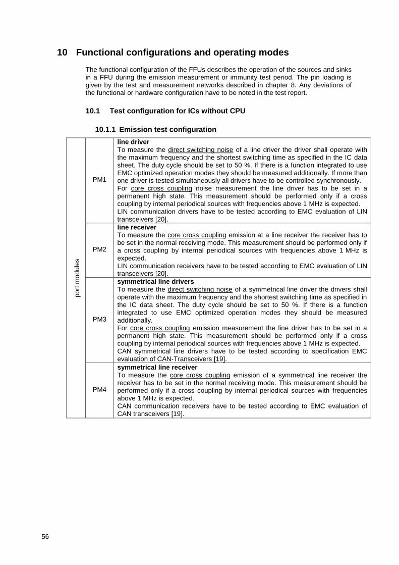
56
10 Functional configurations and operating modes
The functional configuration of the FFUs describes the operation of the sources and sinks in a FFU during the emission measurement or immunity test period. The pin loading is given by the test and measurement networks described in chapter 8. Any deviations of the functional or hardware configuration have to be noted in the test report.
10.1 Test configuration for ICs without CPU
10.1.1 Emission test configuration
port
modu
les
PM1
line driver To measure the direct switching noise of a line driver the driver shall operate with the maximum frequency and the shortest switching time as specified in the IC data sheet. The duty cycle should be set to 50 %. If there is a function integrated to use EMC optimized operation modes they should be measured additionally. If more than one driver is tested simultaneously all drivers have to be controlled synchronously. For core cross coupling noise measurement the line driver has to be set in a permanent high state. This measurement should be performed only if a cross coupling by internal periodical sources with frequencies above 1 MHz is expected. LIN communication drivers have to be tested according to EMC evaluation of LIN transceivers [20].
PM2
line receiver To measure the core cross coupling emission at a line receiver the receiver has to be set in the normal receiving mode. This measurement should be performed only if a cross coupling by internal periodical sources with frequencies above 1 MHz is expected. LIN communication receivers have to be tested according to EMC evaluation of LIN transceivers [20].
PM3
symmetrical line drivers To measure the direct switching noise of a symmetrical line driver the drivers shall operate with the maximum frequency and the shortest switching time as specified in the IC data sheet. The duty cycle should be set to 50 %. If there is a function integrated to use EMC optimized operation modes they should be measured additionally. For core cross coupling emission measurement the line driver has to be set in a permanent high state. This measurement should be performed only if a cross coupling by internal periodical sources with frequencies above 1 MHz is expected. CAN symmetrical line drivers have to be tested according to specification EMC evaluation of CAN-Transceivers [19].
PM4
symmetrical line receiver To measure the core cross coupling emission of a symmetrical line receiver the receiver has to be set in the normal receiving mode. This measurement should be performed only if a cross coupling by internal periodical sources with frequencies above 1 MHz is expected. CAN communication receivers have to be tested according to EMC evaluation of CAN transceivers [19].
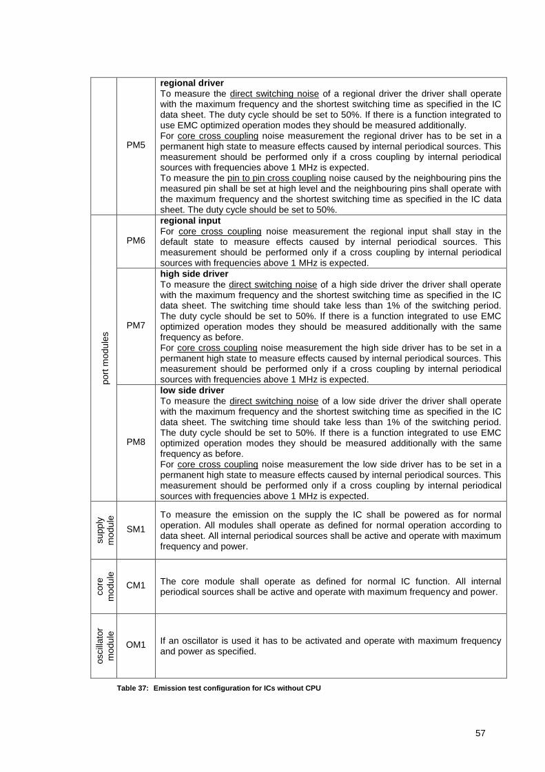
57
PM5
regional driver To measure the direct switching noise of a regional driver the driver shall operate with the maximum frequency and the shortest switching time as specified in the IC data sheet. The duty cycle should be set to 50%. If there is a function integrated to use EMC optimized operation modes they should be measured additionally. For core cross coupling noise measurement the regional driver has to be set in a permanent high state to measure effects caused by internal periodical sources. This measurement should be performed only if a cross coupling by internal periodical sources with frequencies above 1 MHz is expected. To measure the pin to pin cross coupling noise caused by the neighbouring pins the measured pin shall be set at high level and the neighbouring pins shall operate with the maximum frequency and the shortest switching time as specified in the IC data sheet. The duty cycle should be set to 50%.
port
modu
les
PM6
regional input For core cross coupling noise measurement the regional input shall stay in the default state to measure effects caused by internal periodical sources. This measurement should be performed only if a cross coupling by internal periodical sources with frequencies above 1 MHz is expected.
PM7
high side driver To measure the direct switching noise of a high side driver the driver shall operate with the maximum frequency and the shortest switching time as specified in the IC data sheet. The switching time should take less than 1% of the switching period. The duty cycle should be set to 50%. If there is a function integrated to use EMC optimized operation modes they should be measured additionally with the same frequency as before. For core cross coupling noise measurement the high side driver has to be set in a permanent high state to measure effects caused by internal periodical sources. This measurement should be performed only if a cross coupling by internal periodical sources with frequencies above 1 MHz is expected.
PM8
low side driver To measure the direct switching noise of a low side driver the driver shall operate with the maximum frequency and the shortest switching time as specified in the IC data sheet. The switching time should take less than 1% of the switching period. The duty cycle should be set to 50%. If there is a function integrated to use EMC optimized operation modes they should be measured additionally with the same frequency as before. For core cross coupling noise measurement the low side driver has to be set in a permanent high state to measure effects caused by internal periodical sources. This measurement should be performed only if a cross coupling by internal periodical sources with frequencies above 1 MHz is expected.
supply
modu
le
SM1
To measure the emission on the supply the IC shall be powered as for normal operation. All modules shall operate as defined for normal operation according to data sheet. All internal periodical sources shall be active and operate with maximum frequency and power.
core
modu
le
CM1 The core module shall operate as defined for normal IC function. All internal periodical sources shall be active and operate with maximum frequency and power.
oscill
ato
r
modu
le
OM1 If an oscillator is used it has to be activated and operate with maximum frequency and power as specified.
Table 37: Emission test configuration for ICs without CPU
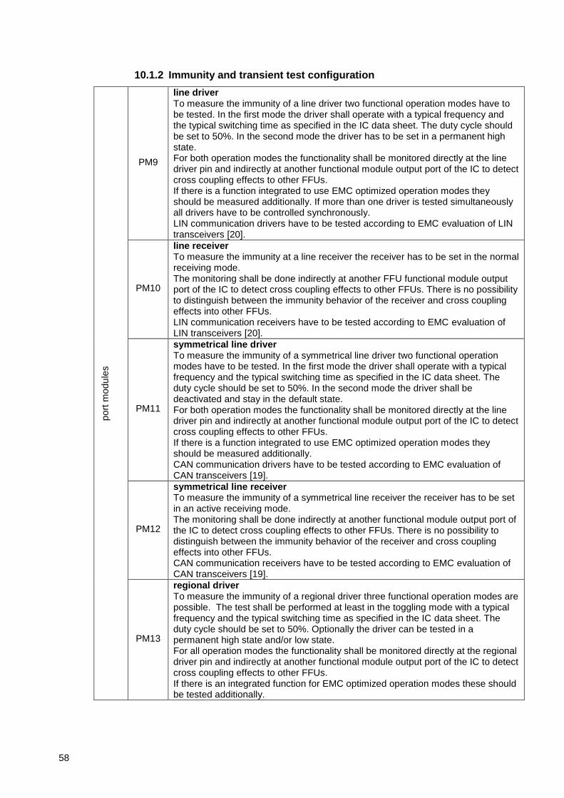
58
10.1.2 Immunity and transient test configuration
port
modu
les
PM9
line driver To measure the immunity of a line driver two functional operation modes have to be tested. In the first mode the driver shall operate with a typical frequency and the typical switching time as specified in the IC data sheet. The duty cycle should be set to 50%. In the second mode the driver has to be set in a permanent high state. For both operation modes the functionality shall be monitored directly at the line driver pin and indirectly at another functional module output port of the IC to detect cross coupling effects to other FFUs. If there is a function integrated to use EMC optimized operation modes they should be measured additionally. If more than one driver is tested simultaneously all drivers have to be controlled synchronously. LIN communication drivers have to be tested according to EMC evaluation of LIN transceivers [20].
PM10
line receiver To measure the immunity at a line receiver the receiver has to be set in the normal receiving mode. The monitoring shall be done indirectly at another FFU functional module output port of the IC to detect cross coupling effects to other FFUs. There is no possibility to distinguish between the immunity behavior of the receiver and cross coupling effects into other FFUs. LIN communication receivers have to be tested according to EMC evaluation of LIN transceivers [20].
PM11
symmetrical line driver To measure the immunity of a symmetrical line driver two functional operation modes have to be tested. In the first mode the driver shall operate with a typical frequency and the typical switching time as specified in the IC data sheet. The duty cycle should be set to 50%. In the second mode the driver shall be deactivated and stay in the default state. For both operation modes the functionality shall be monitored directly at the line driver pin and indirectly at another functional module output port of the IC to detect cross coupling effects to other FFUs. If there is a function integrated to use EMC optimized operation modes they should be measured additionally. CAN communication drivers have to be tested according to EMC evaluation of CAN transceivers [19].
PM12
symmetrical line receiver To measure the immunity of a symmetrical line receiver the receiver has to be set in an active receiving mode. The monitoring shall be done indirectly at another functional module output port of the IC to detect cross coupling effects to other FFUs. There is no possibility to distinguish between the immunity behavior of the receiver and cross coupling effects into other FFUs. CAN communication receivers have to be tested according to EMC evaluation of CAN transceivers [19].
PM13
regional driver To measure the immunity of a regional driver three functional operation modes are possible. The test shall be performed at least in the toggling mode with a typical frequency and the typical switching time as specified in the IC data sheet. The duty cycle should be set to 50%. Optionally the driver can be tested in a permanent high state and/or low state. For all operation modes the functionality shall be monitored directly at the regional driver pin and indirectly at another functional module output port of the IC to detect cross coupling effects to other FFUs. If there is an integrated function for EMC optimized operation modes these should be tested additionally.

59
port
modu
les
PM14
regional input To measure the immunity of a regional input the input has to be set in an active mode. The monitoring shall be done indirectly at another functional module output port of the IC to detect cross coupling effects to other FFUs. There is no possibility to distinguish between the immunity behaviour of the input and cross coupling effects into other FFUs.
PM15
high side driver To measure the immunity of a high side driver three functional operation modes are possible. The test shall be performed at least in the toggling mode with a typical frequency and the typical switching time as specified in the IC data sheet. The duty cycle should be set to 50%. Optionally the driver can be tested in a permanent high state and/or low state. For all operation modes the functionality shall be monitored directly at the high side driver pin and indirectly at another functional module output port of the IC to detect cross coupling effects to other FFUs. If there is an integrated function for EMC optimized operation modes these should be tested additionally.
PM16
low side driver To measure the immunity of a Low Side driver three functional operation modes are possible. The test shall be performed at least in the toggling mode with a typical frequency and the typical switching time as specified in the IC data sheet. The duty cycle should be set to 50%. Optionally the driver can be tested in a permanent high state and/or low state. For all operation modes the functionality shall be monitored directly at the Low Side driver pin and indirectly at another functional module output port of the IC to detect cross coupling effects to other FFUs. If there is an integrated function for EMC optimized operation modes these should be tested additionally.
supply
modu
le
SM2
To measure the immunity of the supply the IC shall be powered for normal operation. All modules shall operate as defined for normal operation according to data sheet. All internal periodical sources shall be active and operate with maximum frequency and power. The monitoring shall be done indirectly at the supplied FFUs of the IC.
core
mod
ule
CM2 core active mode The core module shall operate as defined for normal IC function. All internal functions shall be active and operate with typical frequency and power.
CM3 core sleep modes If it is possible to set the IC in other modes different to the normal mode such as sleep mode, standby mode etc. these should be tested additionally.
oscill
ato
r
modu
le
OM2 If an oscillator is used it has to be activated and operate with typical frequency and power as specified.
Table 38: Immunity test configuration for ICs without CPU

60
10.2 Test configuration for ICs with CPU
10.2.1 Software initialization for emission tests
configuration software module
description and definition of test initialization software module
nu
mb
er
nam
e
sh
ort
descri
pti
on
C1
refe
rence
‘wors
t case’ settin
g
system clock:
- frequency f = fmax
CPU: - active
FFUs: - all Fixed-function Units active, if available: system clock output active
active ports: - all multifunction ports switched to FFU function
- fastest slew rate of drivers
inactive Ports:
- all other ports
memory access:
- choose the memory access for the loop software module with highest emission potential available, for example:
- synchronous access from external memory (burst mode)
- asynchronous access from external memory
- internal access from on-chip memory
C2
bus m
ode
1
pro
gra
m e
xecution w
ith s
ynchro
nous
bus a
ccess/ syste
m c
lock
system clock:
- frequency f = fmax
CPU: - active
FFUs: - all Fixed-function Units inactive, except the memory interface
active ports: - buses
- bus clock (system clock output active)
- fastest slew rate of drivers
inactive Ports:
- all other ports
memory access:
- memory access for the loop software module: synchronous access from external memory (burst mode)
C3 2
pro
gra
m e
xecution w
ith
asynchro
nous b
us a
ccess/
syste
m c
lock
system clock:
- frequency f = fmax
CPU: - active
FFUs: - all Fixed-function Units inactive, except the memory interface
active ports: - buses
- fastest slew rate of drivers
inactive Ports:
- all other ports
- bus clock (System clock output inactive)
memory access:
- memory access for the loop software module: asynchronous access from external memory
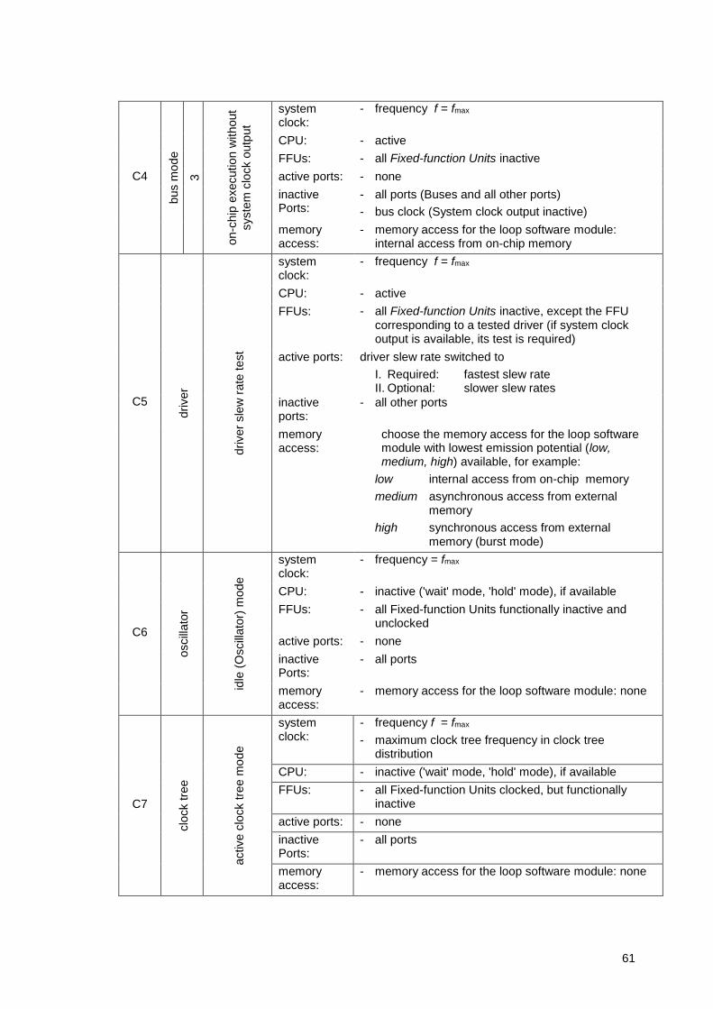
61
C4 bus m
ode
3
on-c
hip
execution w
ithout
syste
m c
lock o
utp
ut
system clock:
- frequency f = fmax
CPU: - active
FFUs: - all Fixed-function Units inactive
active ports: - none
inactive Ports:
- all ports (Buses and all other ports)
- bus clock (System clock output inactive)
memory access:
- memory access for the loop software module: internal access from on-chip memory
C5
driver
driver
sle
w r
ate
test
system clock:
- frequency f = fmax
CPU: - active
FFUs: - all Fixed-function Units inactive, except the FFU corresponding to a tested driver (if system clock output is available, its test is required)
active ports: driver slew rate switched to
I. Required: fastest slew rate II. Optional: slower slew rates
inactive ports:
- all other ports
memory access:
choose the memory access for the loop software module with lowest emission potential (low, medium, high) available, for example:
low internal access from on-chip memory
medium asynchronous access from external memory
high synchronous access from external memory (burst mode)
C6
oscill
ato
r
idle
(O
scill
ato
r) m
ode
system clock:
- frequency = fmax
CPU: - inactive ('wait' mode, 'hold' mode), if available
FFUs: - all Fixed-function Units functionally inactive and unclocked
active ports: - none
inactive Ports:
- all ports
memory access:
- memory access for the loop software module: none
C7
clo
ck t
ree
active c
lock t
ree
mo
de
system clock:
- frequency f = fmax
- maximum clock tree frequency in clock tree distribution
CPU: - inactive ('wait' mode, 'hold' mode), if available
FFUs: - all Fixed-function Units clocked, but functionally inactive
active ports: - none
inactive Ports:
- all ports
memory access:
- memory access for the loop software module: none
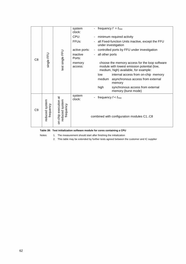
62
C8
sin
gle
FF
U
test sin
gle
FF
U
system clock:
- frequency f = fmax
CPU: - minimum required activity
FFUs: - all Fixed-function Units inactive, except the FFU under investigation
active ports: - controlled ports by FFU under investigation
inactive Ports:
- all other ports
memory access:
choose the memory access for the loop software module with lowest emission potential (low, medium, high) available, for example:
low internal access from on-chip memory
medium asynchronous access from external memory
high synchronous access from external memory (burst mode)
C9
reduced s
yste
m
freque
ncy
on-c
hip
exe
cution a
t
reduced s
yste
m
freque
ncy
system clock:
- frequency f < fmax
combined with configuration modules C1..C8
Table 39: Test initialization software module for cores containing a CPU
Notes: 1. The measurement should start after finishing the initialization
2. This table may be extended by further tests agreed between the customer and IC supplier

63
10.2.2 Software initialization for immunity and transient voltage tests
configuration software module
description and definition of test initialization software module
nu
mb
er
nam
e
sh
ort
descri
pti
on
C10
imm
un
ity r
efe
rence
functiona
l ‘W
ors
t case
’ sett
ing
system clock:
- frequency f = fmax
CPU: - active
FFUs: - all Fixed-function Units active, if available: system clock output active
active ports: - all multifunction ports switched to FFU function
- fastest slew rate of drivers
inactive ports:
- all other ports
monitor pin: - a pin of a non-multifunction port without FFU function, toggle signal with fixed relation to system clock (constant frequency), CPU-driven
error detection:
- all possible error detections should be active (e.g. watchdog, oscillator loss of lock, internal/external bus errors / FFU-errors, traps, interrupts)
- load/compare/store loop inside internal/external memory
- each error case should stop the toggling signal on the monitor pin
memory access:
choose the memory access for the loop software module with highest functional potential (high, medium, low) available, for example:
high synchronous access from external memory (burst mode)
medium asynchronous access from external memory
low internal access from on-chip memory
C11
oscill
ato
r
idle
mode
(oscill
ato
r te
st-
mode)
system clock:
- frequency f = foscillator
CPU: - inactive ('wait' mode, 'hold' mode), if available
FFUs: - all Fixed-function Units functionally inactive and unclocked
OSC: - all different Oscillator-driver-settings must be tested on a typical crystal (e.g. according to data sheet like 4 MHz / 16 MHz)
active ports: - clock output or a toggling port for monitoring
inactive Ports:
- all ports
memory access:
- memory access for the loop software module: none
Table 40: Immunity test configuration for ICs with CPU
Notes: 1. The measurement shall start after finishing the initialization
2. This table may be extended by further tests agreed between the customer and IC supplier

64
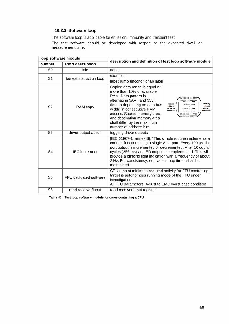
65
10.2.3 Software loop
The software loop is applicable for emission, immunity and transient test.
The test software should be developed with respect to the expected dwell or measurement time.
loop software module description and definition of test loop software module
number short description
S0 idle none
S1 fastest instruction loop example:
label: jump(unconditional) label
S2 RAM copy
Copied data range is equal or more than 10% of available RAM. Data pattern is alternating $AA.. and $55.. (length depending on data bus width) in consecutive RAM access. Source memory area and destination memory area shall differ by the maximum number of address bits
S3 driver output action toggling driver outputs
S4 IEC increment
[IEC 61967-1, annex B]: "This simple routine implements a counter function using a single 8-bit port. Every 100 µs, the port output is incremented or decremented. After 10 count cycles (256 ms) an LED output is complemented. This will provide a blinking light indication with a frequency of about 2 Hz. For consistency, equivalent loop times shall be maintained."
S5 FFU dedicated software
CPU runs at minimum required activity for FFU controlling, target is autonomous running mode of the FFU under investigation All FFU parameters: Adjust to EMC worst case condition
S6 read receiver/input read receiver/input register
Table 41: Test loop software module for cores containing a CPU

66
11 EMC limits for automotive ICs
All relevant pins of an IC shall be classified according to the limits given in the following chapters. Mandatory components are regarded as part of the IC and shall be added for the test.
The limit classes are different depending on the requirements given by the application. The application EMC effort is defined by the application itself, ECU housing, number of layers, filters elements etc.
limit class description
I low EMC requirement
II medium EMC requirement
III high EMC requirement
C customer specific
Table 42: EMC limits for automotive ICs
11.1 RF emission
11.1.1 Emission level scheme
The following level scheme can be used to classify the emission of ICs.
Figure 26: Emission level scheme according to IEC61967-2, IEC61967-4 and IEC61967-8

67
By selecting the right emission level and defining a limit class for a dedicated IC pin the desired functionality and operation mode has to be considered.
Toggling digital data pins, periodically switching analog power outputs etc. generate switching harmonics as a matter of principle. This may violate emission requirements in terms of standard limit classes but cannot be avoided by IC design measures for functional reasons. The resulting spectrum can be obtained by Fourier transformation of the functional specified signal waveform as described in Annex G. This spectrum describes the limitation of the minimal emission and has to be considered to define superimposed specific limits for those pins.
11.1.2 General emission limit classes
limit class 150 method 1 method (G)TEM cell method
IC stripline method global local global local
I 8-H 6-F 10-K 8-H I F
II 10-K 8-H 12-M 10-K L H
III 12-M 10-K 14-O 12-M N K
C customer specific
Table 43: General emission limit classes
Note: Stripline limits are calculated for stripline with septum height of 6,7 mm (16,6 dB) and adapted to the emission level scheme in Figure 26.
A conversion factor (X) to correlate measuring results of IC striplines with different heights to the default IC stripline height of 6,7 mm can be obtained by:
2
1log20h
hX
X = conversion factor in dB to IC stripline 6,7 mm height type results h1 = active conductor height of specific type h2 = active conductor height of 6,7 mm type

68
conducted emission 150 Ω method limit line set for all IC function modules
Figure 27: Limit line set 150 method for global pins
Figure 28: Limit line set 150 method for local pins

69
conducted emission 1 Ω method limit line set for all IC function modules
Figure 29: Limit line set 1 emission test method for global pins
Figure 30: Limit line set 1 emission test method for local pins

70
radiated emission test methods (G)TEM-cell and IC stripline
Figure 31: Limit line set for (G)TEM cell emission test method
Figure 32: Limit line set for IC stripline emission test method
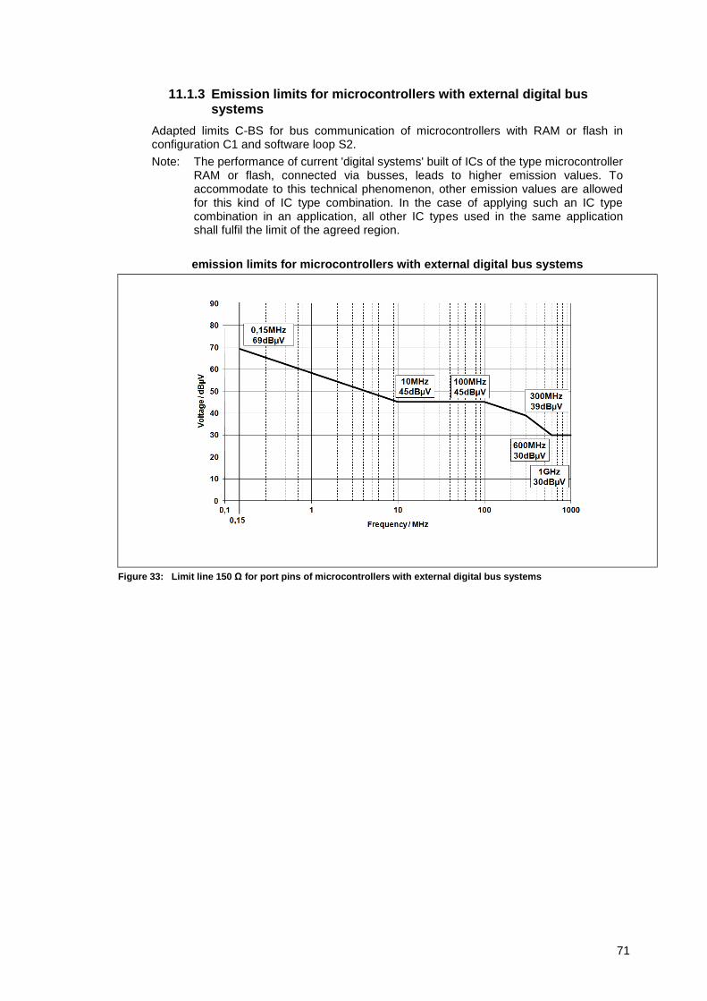
71
11.1.3 Emission limits for microcontrollers with external digital bus systems
Adapted limits C-BS for bus communication of microcontrollers with RAM or flash in configuration C1 and software loop S2.
Note: The performance of current 'digital systems' built of ICs of the type microcontroller RAM or flash, connected via busses, leads to higher emission values. To accommodate to this technical phenomenon, other emission values are allowed for this kind of IC type combination. In the case of applying such an IC type combination in an application, all other IC types used in the same application shall fulfil the limit of the agreed region.
emission limits for microcontrollers with external digital bus systems
Figure 33: Limit line 150 Ω for port pins of microcontrollers with external digital bus systems
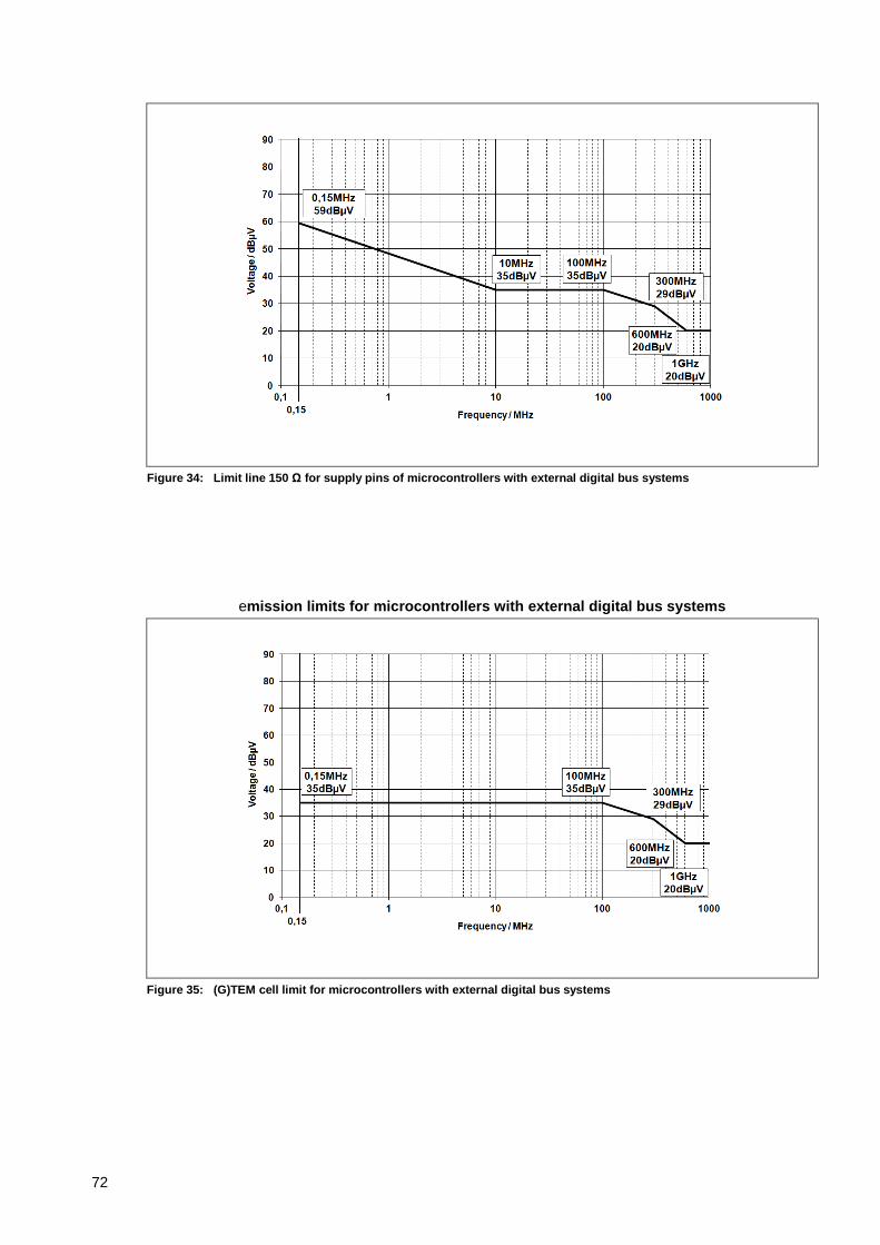
72
Figure 34: Limit line 150 Ω for supply pins of microcontrollers with external digital bus systems
emission limits for microcontrollers with external digital bus systems
Figure 35: (G)TEM cell limit for microcontrollers with external digital bus systems

73
Figure 36: IC Stripline (6,7 mm) limit for microcontrollers with external digital bus systems

74
11.2 RF immunity
11.2.1 General immunity limit classes
immunity limit classes
DPI
forward power / dBm
(G)TEM
E-field / (V/m)
IC stripline
E-field / (V/m)
global pin local pin entire IC entire IC
I 18 0 200 200
II 24 6 400 400
III 30 12 800 800
C customer specific
Table 44: General immunity limit classes
conducted immunity DPI method limit line set for all IC function modules
Figure 37: DPI limit line set for global pins

75
Figure 38: DPI limit line set for local pins
radiated immunity test methods (G)TEM-cell and IC stripline
Figure 39: Limit line set for (G)TEM and IC stripline radiated immunity test method

76
11.3 Pulse immunity
The specified test pulse voltage has to be applied to the pulse injection point. Depending on maximum ratings external protection might be required and test relevance has to be considered.
11.3.1 Preliminary pulse immunity limit classes 12 V
pulse
immunity limit
classes
transient exposure pin category / coupling
performance class
global local
1 2 3 4 5
direct 1nF direct
filtered 1nF
filtered 10pF
ISO 1 I II III
-75 -112 -150
V V V
n/a -75
-112 -150
V V V
n/a n/a CIC
ISO 2a I II III
37 55
112
V V V
n/a 37 55
112
V V V
n/a n/a AIC, CIC
ISO 3a I II III
-112 -165 -220
V V V
-112 -165 -220
V V V
-112 -165 -220
V V V
-112 -165 -220
V V V
-112 -165 -220
V V V
AIC, CIC
ISO 3b I II III
75 112 150
V V V
75 112 150
V V V
75 112 150
V V V
75 112 150
V V V
75 112 150
V VV
AIC, CIC
Table 45: General immunity limit classes 12V
11.3.2 Preliminary pulse immunity limit classes 24V
pulse
immunity limit
classes
transient exposure pin category / coupling
performance class
global local
1 2 3 4 5
direct 1nF direct filtered
1nF filtered
10pF
ISO 1 I II III
-300 -450 -600
V V V
n/a -300 -450 -600
V V V
n/a n/a CIC
ISO 2a I II III
37 55
112
V V V
n/a 37 55
112
V V V
n/a n/a AIC, CIC
ISO 3a I II III
-150 -220 -300
V V V
-150 -220 -300
V V V
-150 -220 -300
V V V
-150 -220 -300
V V V
-150 -220 -300
V V V
AIC, CIC
ISO 3b I II III
150 220 300
V V V
150 220 300
V V V
150 220 300
V V V
150 220 300
V V V
150 220 300
V V V
AIC, CIC
Table 46: General immunity limit classes 24V

77
11.4 System level ESD
11.4.1 Preliminary limits for unpowered system level ESD test
pin type model
ESD generator
discharge network standard ESD class ESD level
C R
global pin HBM
(system level) 150 pF 330 Ω ISO 10605 2nd Ed.
I
II
III
C
2 kV
4 kV
6 kV
customer specific
Table 47: Preliminary limit classes for unpowered system level ESD tests

78
12 IC EMC specification
The IC EMC specification for a dedicated IC is either provided by the customer or by the IC supplier. It contains the pin selection, functional configuration, measurement method and limits (EMC requirements) for emission and immunity tests. Additionally the test board’s schematic and special agreements may be included. Examples are given in Annex F.
13 Test report
Following items shall be part of the test report:
References to used specifications and standards
Schematic diagram of test board
Pictures of test board layout and/or parts of it
Description of external components
Transfer characteristics of RF coupling paths
Functional configurations of FFUs and description of implemented software modules for ICs with CPU
Description of test equipment
Description of monitoring points and failure criteria for immunity and transient voltage tests
Description of any deviation from previously defined test parameters
Result diagrams (emission: scaled in dBµV, immunity: scaled in dBm for DPI or V/m for (G)TEM and IC stripline) including limit lines
Result table for transient and system level ESD tests

79
14 Contacts and authors
The following table shows company contact persons listed in alphabetic order:
Name Company Email address
Felix Mueller Continental Automotive GmbH P.O. Box 10 09 43 93009 Regensburg
Dr. Frank Klotz Infineon Technologies AG Automotive Power – EMC Center 81726 München
Dr. Wolfgang Pfaff Robert Bosch GmbH P.O. Box 300240 70442 Stuttgart
Thomas Steinecke Infineon Technologies AG Automotive Microcontrollers 81726 München
Table 48: List of contact persons
This specification version 2.1 was created by a working group with experts and members of the German national standardization organization DKE from Bosch, Infineon and Continental. The authors are listed in alphabetical order by companies: Robert Bosch GmbH:
Michael Bischoff, Frank Brandl, Dr. Carsten Hermann, Dr. Wolfgang Pfaff Infineon Technologies AG: Dr. Frank Klotz, Thomas Steinecke, Markus Unger Continental Automotive GmbH: Felix Müller, Christian Rödig, Gerhard Schmid Other authors, listed in alphabetical order, have contributed to a previous version of this specification: Dr. Jörg Brückner, Michael Jöster, Herman Roozenbeek, Andreas Rupp, Christoph Schulz-Linkholt.
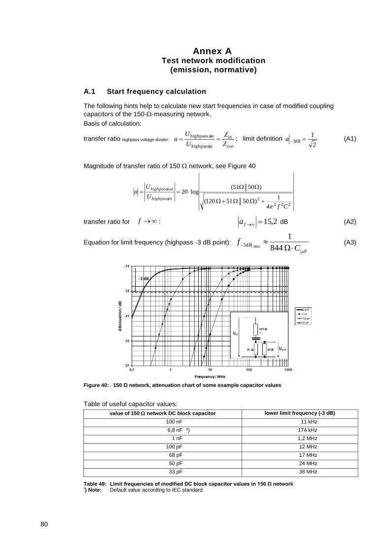
80
Annex A Test network modification
(emission, normative)
A.1 Start frequency calculation
The following hints help to calculate new start frequencies in case of modified coupling
capacitors of the 150--measuring network.
Basis of calculation:
transfer ratio highpass voltage divider out
in
inhighpass,
uthighpass.o
Z
Z
U
Ua ; limit definition
2
1dB3 a (A1)
Magnitude of transfer ratio of 150 network, see Figure 40.
222
2,
,
4
1)5051120(
)5051(log20
Cf
U
Ua
inhighpass
outhighpass
transfer ratio for f : 2,15fa dB (A2)
Equation for limit frequency (highpass -3 dB point):
F
dBC
fMHz
Ω 844
13 (A3)
Figure 40: 150 Ω network, attenuation chart of some example capacitor values
Table of useful capacitor values:
value of 150 network DC block capacitor lower limit frequency (-3 dB)
100 nF 11 kHz
6,8 nF *) 174 kHz
1 nF 1,2 MHz
100 pF 12 MHz
68 pF 17 MHz
50 pF 24 MHz
33 pF 36 MHz
Table 49: Limit frequencies of modified DC block capacitor values in 150 Ω network *) Note: Default value according to IEC standard
81
Annex B Test definition for ICs with RF antenna pins
(normative)
B.1 General
RF antenna pins cannot be tested with conducted IC EMC test methods as defined in [3, 8]. The only exception would be a conducted emission measurement in a 50 Ω system at a 50 Ω matched network directly connected to the RF measuring receiver for information purpose.
Furthermore ICs with RF antenna pins cannot be tested properly with radiated IC EMC test methods as defined in [2, 5, 7, 9]. They have to fulfill special requirements specified in ETSI and FCC for wireless applications. Therefore these special IC types have to be tested similar to the target application in res pect to radiated RF emission and RF immunity.
For ICs targeted for small autarkic wireless applications e.g. remote keyless entry (RKE) or tire pressure monitoring (TPMS) the test effort can be limited to the mandatory radiated tests. Local pin measurements are optional and should be performed only on special request.
B.2 GTEM-cell test board and setup for ICs with RF antenna port
For predicting the IC performance a test board shall be used which carries the IC and all mandatory components but no system components as an antenna. This can be realized with a 50 Ω board which comprises the IC, mandatory elements and a matching network, transforming the impedance of the RF antenna driver/receiver pin to a 50 Ω port. The transformation network has to fulfill the requirements of the IC specification. The 50 Ω port shall be terminated with 50 Ω.
For testing the IC the terminated 50 Ω board is placed in GTEM cell on system level position as shown in Figure 41 and Figure 42, not on IC level position as in [2] and [7]. Therewith, all orientations can be tested. The IC is preferably supplied by a small battery on the test board. The 50 Ω test board as described fully provides emission/sensitivity caused by direct coupling of applied EM fields to the IC or to the mandatory components connected to the IC on the test board without overlaid antenna effects. Therefore this test provides IC level results based on tests similar to application tests without system effects e.g. caused by special antenna characteristics. During test the IC shall be set in a constant transmitting/receiving mode.
B.2.1 Radiated emission test
For radiated emission 24 test directions should be tested, which means 2 positions top/bottom in 4 directions 0°, 90°, 180°, 270° and in each x-, y-, z-orientation. The frequencies of interest are the harmonics of the carrier fcarrier up to the 10th harmonic of fcarrier (2 . fcarrier, 3 . fcarrier,…, 10 . fcarrier ). For each harmonic, the maximum received value is noted of each test direction. Out of all measured radiated field components the equivalent isotropic radiated power (EIRP) value has to be calculated (e.g. with a software tool provided by GTEM cell manufacturer). For one position with the IC in x-orientation (see x_a in Figure 43) a full scan in the frequency range up to 3 GHz shall be performed for information purpose.
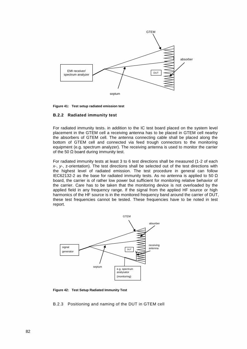
82
Figure 41: Test setup radiated emission test
B.2.2 Radiated immunity test
For radiated immunity tests, in addition to the IC test board placed on the system level placement in the GTEM cell a receiving antenna has to be placed in GTEM cell nearby the absorbers of GTEM cell. The antenna connecting cable shall be placed along the bottom of GTEM cell and connected via feed trough connectors to the monitoring equipment (e.g. spectrum analyzer). The receiving antenna is used to monitor the carrier of the 50 Ω board during immunity test. For radiated immunity tests at least 3 to 6 test directions shall be measured (1-2 of each x-, y-, z-orientation). The test directions shall be selected out of the test directions with the highest level of radiated emission. The test procedure in general can follow IEC62132-2 as the base for radiated immunity tests. As no antenna is applied to 50 Ω board, the carrier is of rather low power but sufficient for monitoring relative behavior of the carrier. Care has to be taken that the monitoring device is not overloaded by the applied field in any frequency range. If the signal from the applied HF source or high harmonics of the HF source is in the monitored frequency band around the carrier of DUT, these test frequencies cannot be tested. These frequencies have to be noted in test report.
Figure 42: Test Setup Radiated Immunity Test
B.2.3 Positioning and naming of the DUT in GTEM cell
septum
signal
generator
absorber
GTEM
e.g. spectrum analysator
(monitoring)
receiving antenna
DUT
septum
EMI receiver/
spectrum analyzer
absorber
GTEM
DUT

83
For positioning of the test board with the DUT up to 24 directions are possible, if a rotation angle of 90 degree is used. Some examples and terms are given in the figures below indicating the x-,y-,z- field orientation and DUT position.
If the main positions of the DUT in respect to RF emission or RF reception are known, the test can be limited to these positions.
Figure 43: DUT Setup position in GTEM cell
septum of GTEM
cross-section of GTEM
orientations: Z_b orientations: Z_a
50 board
IC
50 board
axis of rotation
axis of rotation
IC
septum of GTEM
E-field E-field
50 board
IC
50 board
axis of rotation
axis of rotation
septum of GTEM
septum of GTEM
cross-section of GTEM cross-section of GTEM
orientations: Y_b orientations: Y_a
E-field E-field
IC
septum of GTEM
50 board IC
septum of GTEM
axis of rotation
axis of rotation
50 board
IC
orientations: X_a
E-field E-field
cross-section of GTEM cross-section of GTEM
orientations: X_b
cross-section of GTEM

84
Annex C Layout recommendation
(informative)
C.1 Several networks
C.1.1 Layout example of 150 networks on 2 layer and multi layer PCB
IC
6.8 nF
120
51
SMA or SMBconnector
R1
R2
C1
Conducted Emissionconfiguration
R1 C1
R2
50 micro stripline
length < /20
Signal or supply to IC pin
CX
CX
ZX
ZX
51
120 6.8nF
CX e.g.: Output mode load capacitor or supply buffer capacitor
IC-Pin
ZX e.g.: 0 for connection to circuit or pullup resitor for input mode
= top layer
= bottom layer circuit ground TEM cell RF ground plane
DUT on bottom side Components as closetogether as possible
SMA or SMB connectoron top side
150 network on 2 layer PCB
IC
6.8 nF
120
51
SMA or SMBconnector
R1
R2
C1
Conducted Emissionconfiguration
R1 C1
R2
50 micro stripline
length < /20
Signal or supply to IC pin
CX
CX
ZX
ZX
51
120 6.8nF
CX e.g.: Output mode load capacitor or supply buffer capacitor
IC-Pin
ZX e.g.: 0 for connection to circuit or pullup resitor for input mode
= top layer
.
.
.
.
= 1st inner layer
= other inner layer
= bottom layer reserverd for TEM cell RF ground plane
DUT on bottom side Components as closetogether as possible
SMA or SMB connectoron top side
150 network on multi layer PCB
Figure 44: Layout recommendation 150 Ω network
Notes: The impedance of the signal island at the IC pin is not 150 , but can be neglected as it is as small as possible.
This layout recommendation can be configured to perform Direct Power Injection (DPI) according to IEC62132-4.
The distance of the 50 trace edges to the ground copper edges on the same layer should be
minimal twice of the distance between the 50 trace and the ground plane underneath the trace.
C.1.2 Layout example of 1 network on 2 layer and multi layer PCB
IC
1
1 Probe
Conducted emission
1 method
50 micro stripline
length < /20
DUT on bottom sideSMA or SMB connectoron top side
CDecoupling
IC-ground-pin
= top layer
= bottom layer circuit ground TEM cell RF ground plane
IC sum ground island
VSupply Pin
IC-ground-pin
IC-ground-pin
Groundisland Signal
ground
CDecoupling
VSupply Pin
.
. inner layers
Figure 45: Layout recommendation 1 Ω network
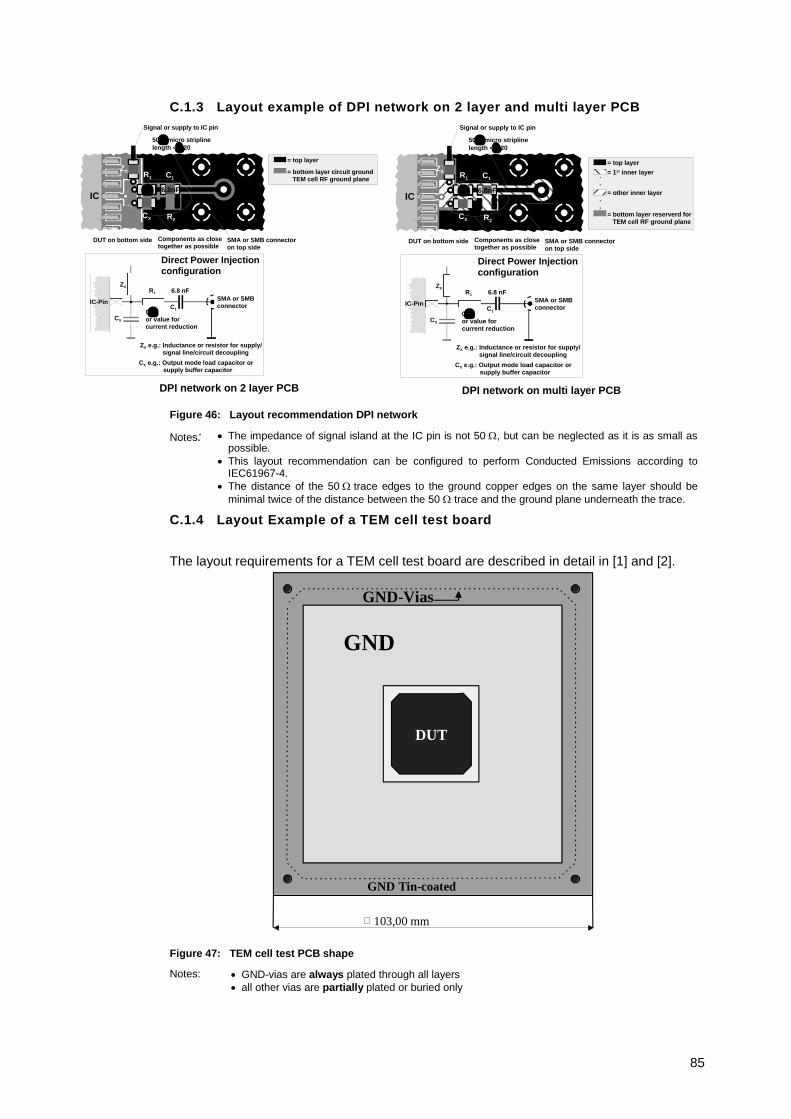
85
C.1.3 Layout example of DPI network on 2 layer and multi layer PCB
IC
6.8 nF
0
or value forcurrent reduction
SMA or SMBconnector
R1
C1
Direct Power Injectionconfiguration
R1 C1
R2
50 micro stripline
length < /20
Components as closetogether as possible
DUT on bottom side
Signal or supply to IC pin
SMA or SMB connectoron top side
CX
CX
ZX
ZX
0 6.8nF
CX e.g.: Output mode load capacitor or supply buffer capacitor
IC-Pin
ZX e.g.: Inductance or resistor for supply/ signal line/circuit decoupling
= top layer
= bottom layer circuit ground TEM cell RF ground plane
DPI network on 2 layer PCB
IC
6.8 nF
0
or value forcurrent reduction
SMA or SMBconnector
R1
C1
Direct Power Injectionconfiguration
R1 C1
R2
50 micro stripline
length < /20
Components as closetogether as possible
DUT on bottom side
Signal or supply to IC pin
SMA or SMB connectoron top side
CX
CX
ZX
ZX
0 6.8nF
CX e.g.: Output mode load capacitor or supply buffer capacitor
IC-Pin
ZX e.g.: Inductance or resistor for supply/ signal line/circuit decoupling
= top layer
.
.
.
.
= 1st inner layer
= other inner layer
= bottom layer reserverd for TEM cell RF ground plane
DPI network on multi layer PCB
Figure 46: Layout recommendation DPI network
Notes: The impedance of signal island at the IC pin is not 50 , but can be neglected as it is as small as possible.
This layout recommendation can be configured to perform Conducted Emissions according to IEC61967-4.
The distance of the 50 trace edges to the ground copper edges on the same layer should be
minimal twice of the distance between the 50 trace and the ground plane underneath the trace.
C.1.4 Layout Example of a TEM cell test board
The layout requirements for a TEM cell test board are described in detail in [1] and [2].
DUT
GND-Vias
GND Tin-coated
GND
103,00 mm
GND-Vias are always plated through all layers and all
other Vias are partial plated or buried only.
Figure 47: TEM cell test PCB shape
Notes: GND-vias are always plated through all layers
all other vias are partially plated or buried only
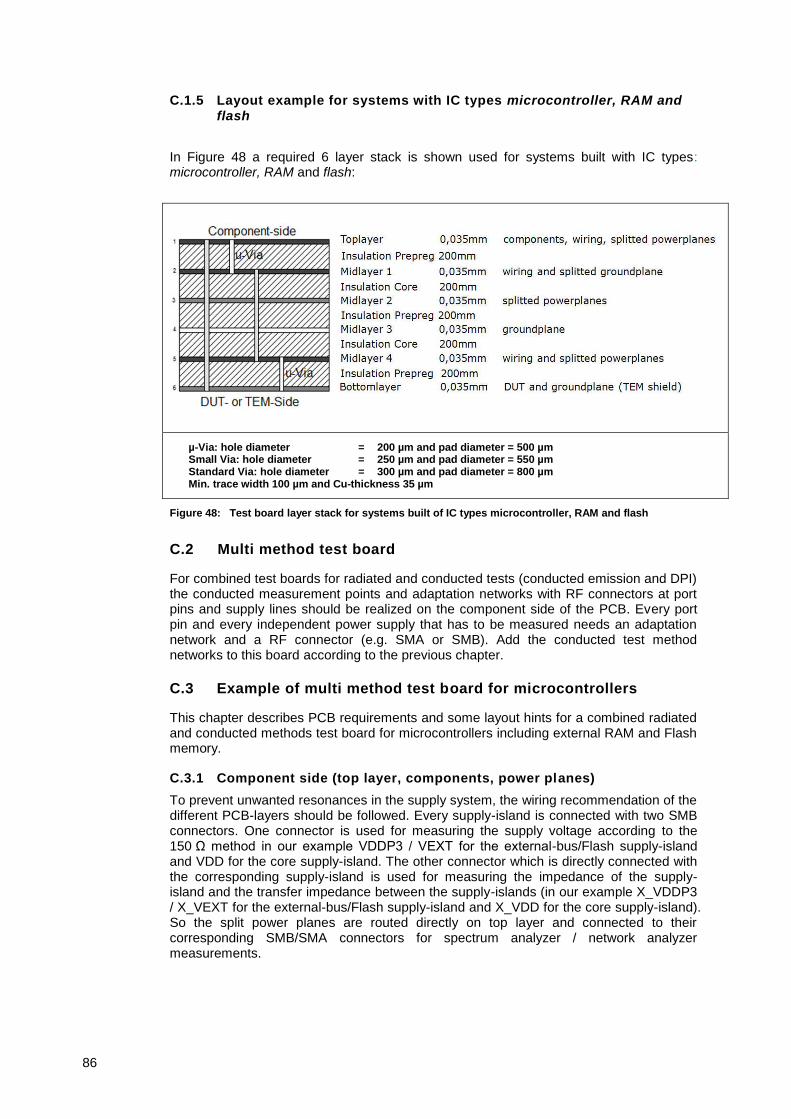
86
C.1.5 Layout example for systems with IC types microcontroller, RAM and flash
In Figure 48 a required 6 layer stack is shown used for systems built with IC types: microcontroller, RAM and flash:
µ-Via: hole diameter = 200 µm and pad diameter = 500 µm Small Via: hole diameter = 250 µm and pad diameter = 550 µm Standard Via: hole diameter = 300 µm and pad diameter = 800 µm Min. trace width 100 µm and Cu-thickness 35 µm
Figure 48: Test board layer stack for systems built of IC types microcontroller, RAM and flash
C.2 Multi method test board
For combined test boards for radiated and conducted tests (conducted emission and DPI) the conducted measurement points and adaptation networks with RF connectors at port pins and supply lines should be realized on the component side of the PCB. Every port pin and every independent power supply that has to be measured needs an adaptation network and a RF connector (e.g. SMA or SMB). Add the conducted test method networks to this board according to the previous chapter.
C.3 Example of multi method test board for microcontrollers
This chapter describes PCB requirements and some layout hints for a combined radiated and conducted methods test board for microcontrollers including external RAM and Flash memory.
C.3.1 Component side (top layer, components, power planes)
To prevent unwanted resonances in the supply system, the wiring recommendation of the different PCB-layers should be followed. Every supply-island is connected with two SMB connectors. One connector is used for measuring the supply voltage according to the 150 Ω method in our example VDDP3 / VEXT for the external-bus/Flash supply-island and VDD for the core supply-island. The other connector which is directly connected with the corresponding supply-island is used for measuring the impedance of the supply-island and the transfer impedance between the supply-islands (in our example X_VDDP3 / X_VEXT for the external-bus/Flash supply-island and X_VDD for the core supply-island). So the split power planes are routed directly on top layer and connected to their corresponding SMB/SMA connectors for spectrum analyzer / network analyzer measurements.

87
Figure 49: Component side
An integrated voltage regulator has to be placed on the test-board, too. Separated supply-lines to the different islands and component units should be used. Only plated-through holes through all layers and no partial vias shall be used for ground connections. For all other connections only partial vias are allowed. Bus wiring should be limited on component layer and inner layer 4 only. Any wiring between core decoupling capacitors at the component side should be prevented.
Figure 50: Detail of component side layer
The supply islands are connected by a special land to the supply line at the component side, which makes it possible to separate the island from the supply line very easily. Such an island is shown below in a picture detail of the component side layer.
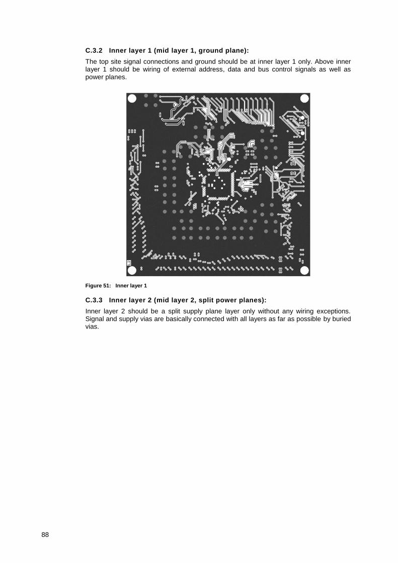
88
C.3.2 Inner layer 1 (mid layer 1, ground plane):
The top site signal connections and ground should be at inner layer 1 only. Above inner layer 1 should be wiring of external address, data and bus control signals as well as power planes.
Figure 51: Inner layer 1
C.3.3 Inner layer 2 (mid layer 2, split power planes):
Inner layer 2 should be a split supply plane layer only without any wiring exceptions. Signal and supply vias are basically connected with all layers as far as possible by buried vias.

89
Figure 52: Inner layer 2
C.3.4 Inner layer 3 (mid layer 3, ground plane) :
The main ground island can be placed more favorable at the inner layer 3 with access to buried vias and through hole vias.
Figure 53: Inner layer 3
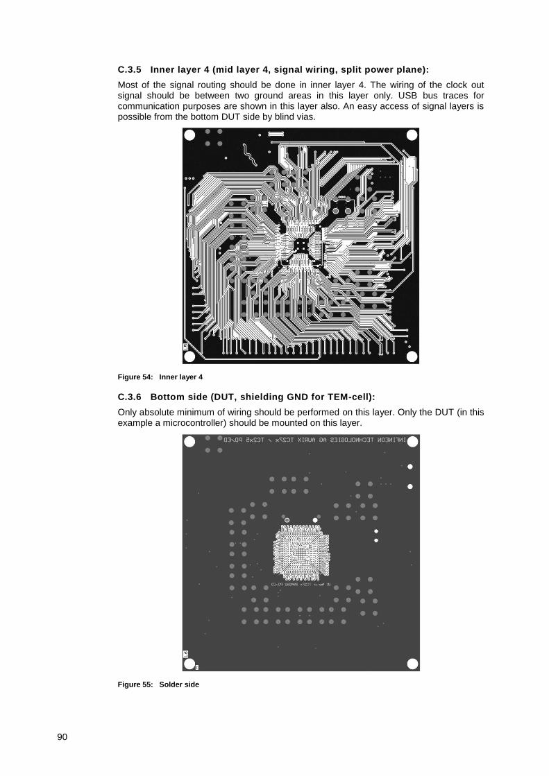
90
C.3.5 Inner layer 4 (mid layer 4, signal wiring, split power plane):
Most of the signal routing should be done in inner layer 4. The wiring of the clock out signal should be between two ground areas in this layer only. USB bus traces for communication purposes are shown in this layer also. An easy access of signal layers is possible from the bottom DUT side by blind vias.
Figure 54: Inner layer 4
C.3.6 Bottom side (DUT, shielding GND for TEM-cell):
Only absolute minimum of wiring should be performed on this layer. Only the DUT (in this example a microcontroller) should be mounted on this layer.
Figure 55: Solder side

91
C.4 Layout examples of system level ESD test boards
An example of a system level ESD test board with soldered IC used for testing global pins of transceiver ICs is shown in Figure 56.
Figure 56: Example of system level ESD test board with soldered IC in top- and bottom layer view
Figure 57: Example of system level ESD test board and fixture
An example of a system level ESD test board with IC connected via socket and external components is shown in Figure 59 to Figure 63.
µ-via (e.g. for BGA socket) : hole diameter = 200-250 µm and pad diameter = 500 µm small via (DC-sweep) : hole diameter = 500 µm and pad diameter = 800 µm ESD discharge via (24A) : hole diameter = 800 µm and pad diameter = 1600 µm discharge point diameter 3mm and Cu-thickness 35 µm min. 1mm clearance around discharge points min. trace width 800 µm and Cu-thickness 35 µm at primary discharge path (24A) min. 250µm clearance around power planes (outer part) min. trace width 250 µm and Cu-thickness 35 µm for power traces (outer part) min. 100µm clearance around power planes (for plane fills inner part like BGA) min. trace width 100 µm and Cu-thickness 35 µm for signal / power traces (inner part like BGA for fanout)
Figure 58: Recommended 4 layer stack up of a test board for IC type microcontroller
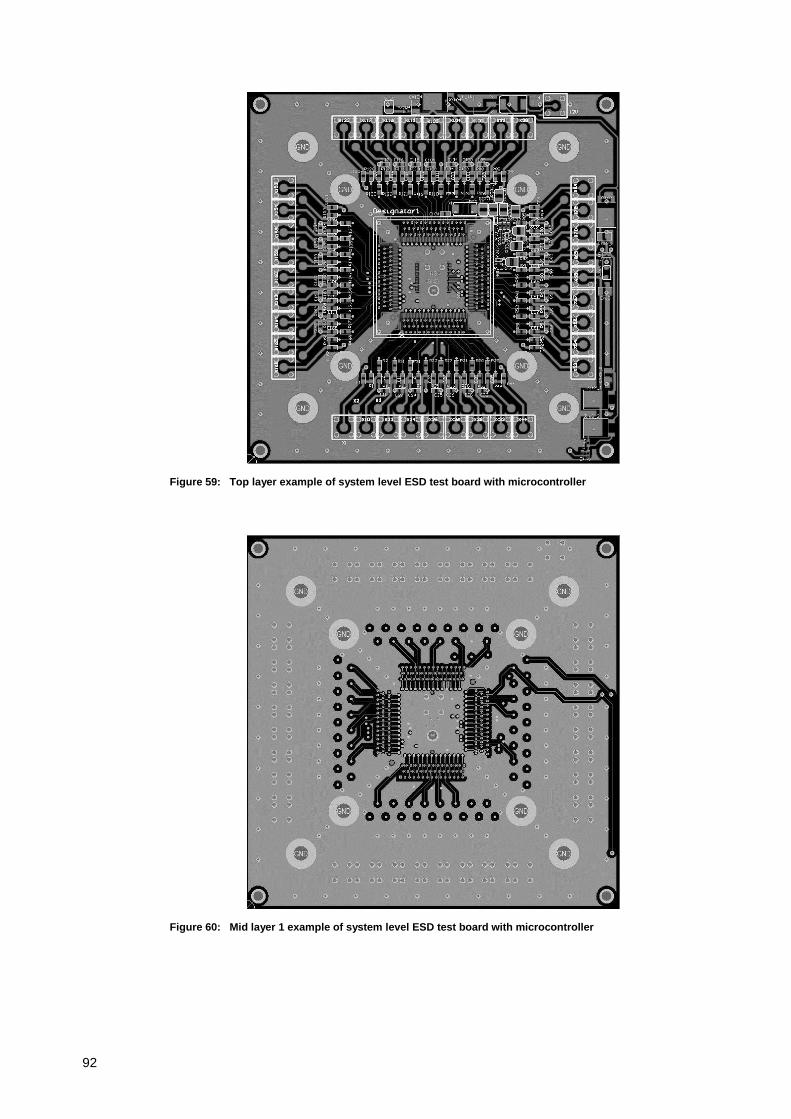
92
Figure 59: Top layer example of system level ESD test board with microcontroller
Figure 60: Mid layer 1 example of system level ESD test board with microcontroller

93
Figure 61: Mid layer 2 example of system level ESD test board with microcontroller
Figure 62: Bottom layer example of system level ESD test board with microcontroller

94
Figure 63: Example of system level ESD test board with IC connected via socket
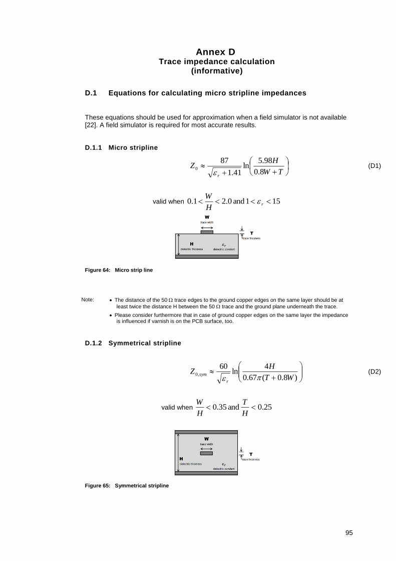
95
Annex D Trace impedance calculation
(informative)
D.1 Equations for calculating micro stripline impedances
These equations should be used for approximation when a field simulator is not available [22]. A field simulator is required for most accurate results.
D.1.1 Micro stripline
TW
HZ
r8.0
98.5ln
41.1
870
(D1)
valid when 151 and 0.21.0 rH
W
Figure 64: Micro strip line
Note: The distance of the 50 trace edges to the ground copper edges on the same layer should be at
least twice the distance H between the 50 trace and the ground plane underneath the trace.
Please consider furthermore that in case of ground copper edges on the same layer the impedance is influenced if varnish is on the PCB surface, too.
D.1.2 Symmetrical stripline
)8.0(67.0
4ln
60,0
WT
HZ
r
sym
(D2)
valid when 25.0 and 35.0 H
T
H
W
Figure 65: Symmetrical stripline

96
D.1.3 Offset stripline
The impedance for an offset stripline is calculated from the results of the symmetrical strip line formulas. The reader should note that this formula D3 is an approximation and the accuracy of the results should be treated as such. For more accurate results, use a field solver.
rr
rr
TWBZTWAZ
TWBZTWAZZ
symsym
symsym
offset
,,,2,,,2
,,,2,,,22
00
00
0
(D3)
Figure 66: Offset stripline
Note: The distance of the 50 trace edges to the ground copper edges on the same layer should be at least
H/2 (Figure 65) or B (Figure 66) between the 50 trace and the ground plane underneath/above the trace.

97
Annex E
Modulation definition for immunity tests (informative)
This annex describes the principle of constant peak test level conservation for modulated signals according to ISO11452-1.
Example for electric field strength:
The electric field strength of the continuous wave (CW) signal, CWE may be written in
the form
)cos( tEE CWCW
with CWE
peak value of CWE
The mean power may be calculated to
2
2CW
CW
EkP
with k proportionality factor depending on the specific test setup, e.g.
Z
hk
2
for the IC stripline with h height of stripline and 50RZ source impedance.
The electric field strength of an amplitude modulated (AM) signal, AME may be written
in the form
)cos()cos1( ttmEE CWAM
with modulation frequency, e.g. 12 kHz.
Where the peak value is
)1( mEE CWAM
The mean power can be calculated by
22
221 CW
AM
EmkP
Note: The total power is the sum of the power in the carrier component and the power in the side- frequency component.
The peak test level preservation may be written as
AMpeakCWpeak EE

98
The relation between CW mean power and AM mean power is then
2
221
2
2'2
E
Em
P
P
CW
AM
2
2
'2
)1(
21
21
m
m
E
Em
Therefore
2
2
)1(2
2
m
mPP CWAM
For 8,0m (AM 80%) this relation gives CWAM PP 407,0
In all these formula m is the modulation index, other symbols are explained in the
relevant parts of ISO11452.
The electric field strength of an pulse modulated (PM) signal, PME may be written in the
form
on
onCW
PM
T
T
TtE
E
0
0)cos(
with Ton and T according to figure 67.
The r.m.s. value of PME is
2
0cos11
,
0
2
0
2 CWon
TT
PMrmsPM
E
T
TdttE
TdtE
TE
on
And the mean power can be written as
2
2
CWonPM
E
T
TkP
For sT 5770 and sT 6004 this relation gives CWPM PP 125,0
CW AM 80 %, 1 kHz
t = 577 µs
t = 4600 µs
PM
Figure 67: CW signal, AM signal and PM signal for constant peak test level
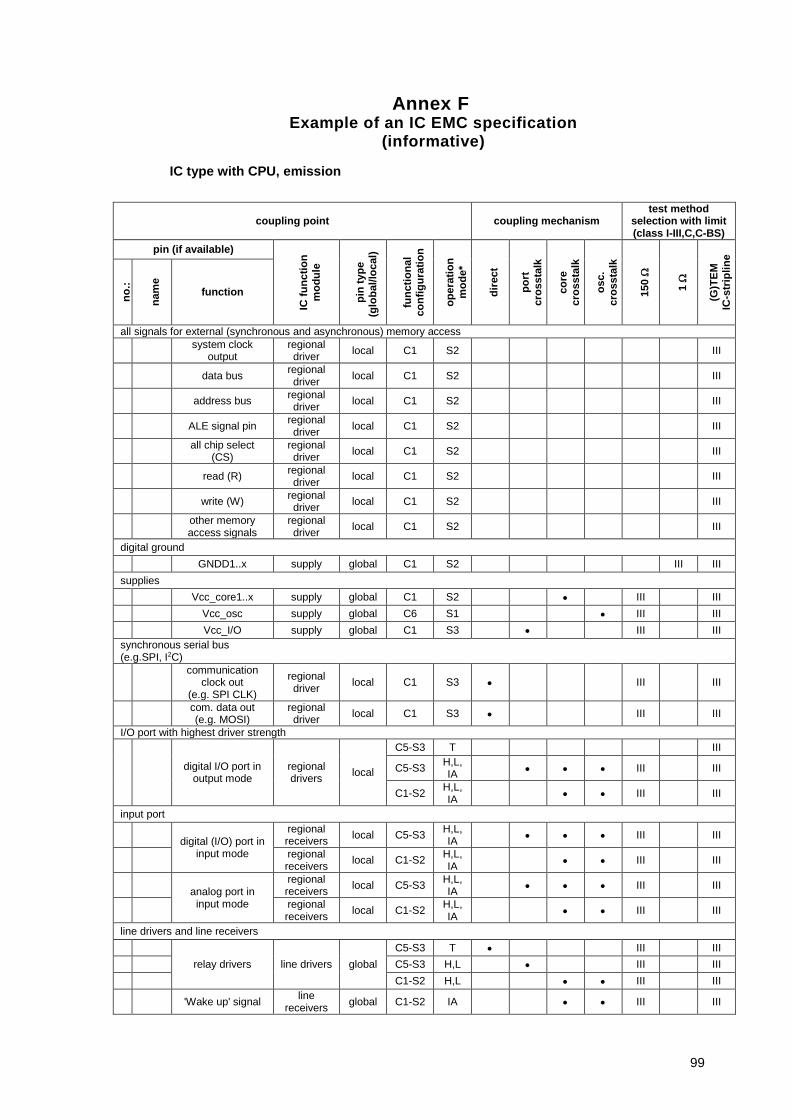
99
Annex F Example of an IC EMC specification
(informative)
IC type with CPU, emission
coupling point coupling mechanism test method
selection with limit (class I-III,C,C-BS)
pin (if available)
IC f
un
cti
on
mo
du
le
pin
typ
e
(glo
ba
l/lo
cal)
fun
cti
on
al
co
nfi
gu
rati
on
op
era
tio
n
mo
de
*
dir
ect
po
rt
cro
ssta
lk
co
re
cro
ssta
lk
os
c.
cro
ssta
lk
150
1
(G)T
EM
IC
-str
iplin
e
no
.:
nam
e
function
all signals for external (synchronous and asynchronous) memory access
system clock
output regional driver
local C1 S2 III
data bus regional driver
local C1 S2 III
address bus regional driver
local C1 S2 III
ALE signal pin regional driver
local C1 S2 III
all chip select
(CS) regional driver
local C1 S2 III
read (R) regional driver
local C1 S2 III
write (W) regional driver
local C1 S2 III
other memory access signals
regional driver
local C1 S2 III
digital ground
GNDD1..x supply global C1 S2 III III
supplies
Vcc_core1..x supply global C1 S2 III III
Vcc_osc supply global C6 S1 III III
Vcc_I/O supply global C1 S3 III III
synchronous serial bus (e.g.SPI, I2C)
communication
clock out (e.g. SPI CLK)
regional driver
local C1 S3 III III
com. data out (e.g. MOSI)
regional driver
local C1 S3 III III
I/O port with highest driver strength
digital I/O port in
output mode regional drivers
local
C5-S3 T III
C5-S3 H,L, IA
III III
C1-S2 H,L, IA
III III
input port
digital (I/O) port in
input mode
regional receivers
local C5-S3 H,L, IA
III III
regional receivers
local C1-S2 H,L, IA
III III
analog port in input mode
regional receivers
local C5-S3 H,L, IA
III III
regional receivers
local C1-S2 H,L, IA
III III
line drivers and line receivers
relay drivers line drivers global
C5-S3 T III III
C5-S3 H,L III III
C1-S2 H,L III III
'Wake up' signal line
receivers global C1-S2 IA III III
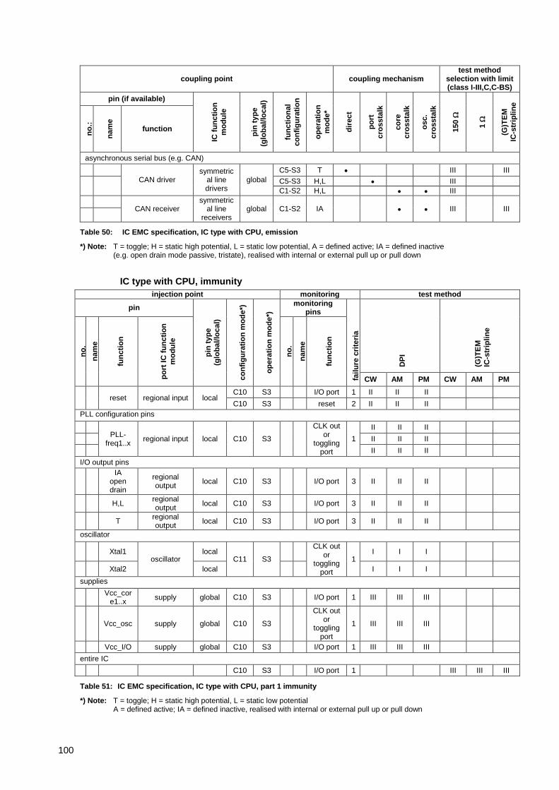
100
coupling point coupling mechanism test method
selection with limit (class I-III,C,C-BS)
pin (if available)
IC f
un
cti
on
mo
du
le
pin
typ
e
(glo
ba
l/lo
cal)
fun
cti
on
al
co
nfi
gu
rati
on
op
era
tio
n
mo
de
*
dir
ect
po
rt
cro
ssta
lk
co
re
cro
ssta
lk
os
c.
cro
ssta
lk
150
1
(G)T
EM
IC
-str
iplin
e
no
.:
nam
e
function
asynchronous serial bus (e.g. CAN)
CAN driver symmetric
al line drivers
global
C5-S3 T III III
C5-S3 H,L III
C1-S2 H,L III
CAN receiver
symmetrical line
receivers global C1-S2 IA III III
Table 50: IC EMC specification, IC type with CPU, emission
*) Note: T = toggle; H = static high potential, L = static low potential, A = defined active; IA = defined inactive (e.g. open drain mode passive, tristate), realised with internal or external pull up or pull down
IC type with CPU, immunity
injection point monitoring test method
pin
pin
typ
e
(glo
ba
l/lo
cal)
co
nfi
gu
rati
on
mo
de
*)
op
era
tio
n m
od
e*)
monitoring pins
fail
ure
cri
teri
a
DP
I
(G)T
EM
IC-s
trip
lin
e
no
.
nam
e
fun
cti
on
po
rt I
C f
un
cti
on
mo
du
le
no
.
nam
e
fun
cti
on
CW AM PM CW AM PM
reset regional input local C10 S3 I/O port 1 II II II
C10 S3 reset 2 II II II
PLL configuration pins
PLL-
freq1..x regional input local C10 S3
CLK out or
toggling port
1
II II II
II II II
II II II
I/O output pins
IA
open drain
regional output
local C10 S3 I/O port 3 II II II
H,L regional output
local C10 S3 I/O port 3 II II II
T regional output
local C10 S3 I/O port 3 II II II
oscillator
Xtal1 oscillator
local C11 S3
CLK out
or toggling
port
1 I I I
Xtal2 local I I I
supplies
Vcc_cor
e1..x supply global C10 S3 I/O port 1 III III III
Vcc_osc supply global C10 S3
CLK out or
toggling port
1 III III III
Vcc_I/O supply global C10 S3 I/O port 1 III III III
entire IC
C10 S3 I/O port 1 III III III
Table 51: IC EMC specification, IC type with CPU, part 1 immunity
*) Note: T = toggle; H = static high potential, L = static low potential A = defined active; IA = defined inactive, realised with internal or external pull up or pull down

101
Failure criteria
failure criterion no. monitored function failure criteria
1 toggling port frequency ±3%
2 voltage at pin as specified in data sheet ±10%
Table 52: IC EMC specification, IC type with CPU, part 2 failure criteria
Pulse immunity
injection point monitoring test method
pin
pin
typ
e
(glo
ba
l/lo
cal)
fun
cti
on
al
co
nfi
gu
rati
on
op
era
tio
n m
od
e*)
monitoring pins
fail
ure
cri
teri
a
tran
sie
nts
on
su
pp
ly
no
.
na
me
fun
cti
on
po
rt I
C f
un
cti
on
mo
du
le
no
.
na
me
fun
cti
on
example:
reset regional
input local
C1-S2 A I/O Port 1 III
C1-S2 A reset 2 III
PLL-
freq1..x regional
input local C1-S2 A
CLK out or toggling port
1
III
III
III
Table 53: Structure of an IC EMC specification, part 1 pulse immunity
*) Note: T = toggle; H = static high potential, L = static low potential A = defined active; IA = defined inactive, realized with internal or external pull up or pull down
Failure criteria
failure criterion no. monitored function failure criteria
1 toggling port frequency ±3%
2 voltage at pin as specified in data sheet ±10%
Table 54: Structure of an IC EMC specification, part 2 pulse immunity
System level ESD
pin no.
name function external components ESD Level
example:
3 OUT low side driver none I
7 VCC supply 100 nF to GND II
12 LIN line driver diode III
Table 55: Structure of an IC EMC specification, part system level ESD

102
Annex G Calculation of pin specific limits
(informative)
G.1 Fourier transformation of time domain signals
Toggling digital data pins or periodically switching analog power outputs generate switching harmonics as a matter of principle defined by the functionally necessary and specified signal waveform. The resulting harmonics of those wanted signal waveforms can be calculated with Fourier-transformation.
For trapezoidal periodic signals as shown in Figure 68, the envelope of the resulting amplitude versus frequency spectrum can be subdivided into 3 sections. From the fundamental frequency of the signal up to the first corner frequency fg1 the spectral response is parallel with the frequency axis. After the first corner frequency fg1 the amplitudes diminish up to the second corner frequency fg2 with 20 dB/decade. From this point the spectrum decreases with 40 dB/decade, as shown in Figure 68. The simplified equations to calculate amplitudes and corner frequencies of the spectrum are shown in Figure 69. AO is defined as the amplitude of original signal (I or V), ti as the signal pulse width, ts as the switching time, TO as the period of the fundamental frequency and n as the multiples of the fundamental frequency.
A0
0
ti
tsts T
2+
T
2-
Time
Amplitude
A0
2
T
Figure 68: Periodical trapezoidal signal, time domain

103
Figure 69: Fourier analysis of periodical signals (simplified calculation)
sn
t
T
nAA 0
220
12
sg
tf
12
ig
tf
11
nAAn
120
0
02
T
tAA i
n
104
15 List of figures
Figure 1: Common definition of an IC function module 10
Figure 2: General test parameters: Immunity, definition of AM modulation carrier 17
Figure 3: General test parameters: Immunity, definition of PM modulation carrier 17
Figure 4: Port module 19
Figure 5: Supply module 20
Figure 6: Core module 21
Figure 7: Oscillator module 22
Figure 8: Example of a Memory IC built up with the IC function modules 24
Figure 9: Test and measurement networks for line driver 32
Figure 10: Test and measurement networks for line receiver 34
Figure 11: Test and measurement networks for symmetrical line driver 35
Figure 12: Test and measurement networks for symmetrical line receiver 36
Figure 13: Test and measurement networks for regional driver 37
Figure 14: Test and measurement networks for regional input 39
Figure 15: Test and measurement networks for high side driver 40
Figure 16: Test and measurement networks for low side driver 43
Figure 17: Test and measurement network supply modules 46
Figure 18: Test and measurement networks oscillator module 48
Figure 19: Test network for unpowered system ESD test on global pin 49
Figure 20: DUT monitoring 50
Figure 21: General setup for a decoupling network for monitoring 51
Figure 22: Decoupling network for monitoring: transfer functions for low pass circuitry examples 52
Figure 23: Example of "Direction x" and "Direction y" of TEM cell test PCB 53
Figure 24: Example of "Direction X" and "Direction Y" of IC stripline test PCB 53
Figure 25: System level ESD test setup 54
Figure 26: Emission level scheme according to IEC61967-2, IEC61967-4 and IEC61967-8 66
Figure 27: Limit line set 150 method for global pins 68
Figure 28: Limit line set 150 method for local pins 68
Figure 29: Limit line set 1 emission test method for global pins 69
Figure 30: Limit line set 1 emission test method for local pins 69
Figure 31: Limit line set for (G)TEM cell emission test method 70
Figure 32: Limit line set for IC stripline emission test method 70
Figure 33: Limit line 150 Ω for port pins of microcontrollers with external digital bus systems 71
Figure 34: Limit line 150 Ω for supply pins of microcontrollers with external digital bus systems 72
Figure 35: (G)TEM cell limit for microcontrollers with external digital bus systems 72
Figure 36: IC Stripline (6,7 mm) limit for microcontrollers with external digital bus systems 73
Figure 37: DPI limit line set for global pins 74
Figure 38: DPI limit line set for local pins 75
Figure 39: Limit line set for (G)TEM and IC stripline radiated immunity test method 75
Figure 40: 150 Ω network, attenuation chart of some example capacitor values 80
Figure 41: Test setup radiated emission test 82
Figure 42: Test Setup Radiated Immunity Test 82
105
Figure 43: DUT Setup position in GTEM cell 83
Figure 44: Layout recommendation 150 Ω network 84
Figure 45: Layout recommendation 1 Ω network 84
Figure 46: Layout recommendation DPI network 85
Figure 47: TEM cell test PCB shape 85
Figure 48: Test board layer stack for systems built of IC types microcontroller, RAM and flash 86
Figure 49: Component side 87
Figure 50: Detail of component side layer 87
Figure 51: Inner layer 1 88
Figure 52: Inner layer 2 89
Figure 53: Inner layer 3 89
Figure 54: Inner layer 4 90
Figure 55: Solder side 90
Figure 56: Example of system level ESD test board with soldered IC in top- and bottom layer view 91
Figure 57: Example of system level ESD test board and fixture 91
Figure 58: Recommended 4 layer stack up of a test board for IC type microcontroller 91
Figure 59: Top layer example of system level ESD test board with microcontroller 92
Figure 60: Mid layer 1 example of system level ESD test board with microcontroller 92
Figure 61: Mid layer 2 example of system level ESD test board with microcontroller 93
Figure 62: Bottom layer example of system level ESD test board with microcontroller 93
Figure 63: Example of system level ESD test board with IC connected via socket 94
Figure 64: Micro strip line 95
Figure 65: Symmetrical stripline 95
Figure 66: Offset stripline 96
Figure 67: CW signal, AM signal and PM signal for constant peak test level 98
Figure 68: Periodical trapezoidal signal, time domain 102
Figure 69: Fourier analysis of periodical signals (simplified calculation) 103
106
16 List of Tables
Table 1: Workflow to perform IC EMC measurements 13
Table 2: Conducted test methods 14
Table 3: Radiated test methods 14
Table 4: Transient test methods 14
Table 5: ESD Test methods 14
Table 6: General test parameters: Emission with RF receiver 15
Table 7: General test parameters: Emission with RF analyser 15
Table 8: General test parameters for immunity 16
Table 9: Modulation frequency ranges 16
Table 10: Pulse parameter definitions 17
Table 11: ESD test definition 18
Table 12: Test procedure system level ESD 18
Table 13: Matrix showing which typical IC function module is integrated in several well known ICs 23
Table 14: Conducted tests: Coupling and injection points 25
Table 15: Selection guide conducted RF emission 26
Table 16: Selection guide conducted RF immunity 27
Table 17: Pulse affected pins according to IEC62215-3 28
Table 18: IC function module to transient exposure pin category matrix 28
Table 19: Transient immunity test circuit selection 29
Table 20: Selection guide conducted transient immunity 30
Table 21: Selection guide radiated emission 31
Table 22: Selection guide radiated immunity 31
Table 23: Network for emission, immunity and transients tests for IC module line driver33
Table 24: Network for immunity and transients tests for IC module line receiver 34
Table 25: Network for emission, immunity and transients tests for IC module symmetrical line driver 35
Table 26: Network for immunity and transients tests for IC module symmetrical line receiver 36
Table 27: Network for emission, immunity and transients tests for IC module regional driver 38
Table 28: Network for immunity and transients tests for IC module regional input 39
Table 29: Network for emission, immunity and transients tests for IC module high side driver 42
Table 30: Network for emission and immunity tests for IC module low side driver 45
Table 31: Network for emission and immunity tests for IC module supply 47
Table 32: Network for immunity tests for IC module oscillator 48
Table 33: External components global supply pin 49
Table 34: External components global port pin 49
Table 35: Example of a failure criteria table 51
Table 36: Definition of performance classes 52
Table 37: Emission test configuration for ICs without CPU 57
Table 38: Immunity test configuration for ICs without CPU 59
Table 39: Test initialization software module for cores containing a CPU 62
Table 40: Immunity test configuration for ICs with CPU 63
Table 41: Test loop software module for cores containing a CPU 65
Table 42: EMC limits for automotive ICs 66
Table 43: General emission limit classes 67

107
Table 44: General immunity limit classes 74
Table 45: General immunity limit classes 12V 76
Table 46: General immunity limit classes 24V 76
Table 47: Preliminary limit classes for unpowered system level ESD tests 77
Table 48: List of contact persons 79
Table 49: Limit frequencies of modified DC block capacitor values in 150 Ω network 80
Table 50: IC EMC specification, IC type with CPU, emission 100
Table 51: IC EMC specification, IC type with CPU, part 1 immunity 100
Table 52: IC EMC specification, IC type with CPU, part 2 failure criteria 101
Table 53: Structure of an IC EMC specification, part 1 pulse immunity 101
Table 54: Structure of an IC EMC specification, part 2 pulse immunity 101
Table 55: Structure of an IC EMC specification, part system level ESD 101

108
ZVEI - German Electrical and Electronic Manufacturers’ Association Electronic Components and Systems Division Lyoner Strasse 9 60528 Frankfurt am Main, Germany
Phone: +49 69 6302-276 Fax: +49 69 6302-407 E-mail: [email protected] www.zvei.org/ecs