emt 251/4 introduction to ic design - unimap...
TRANSCRIPT
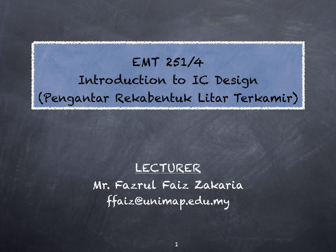
EMT 251/4!Introduction to IC Design!
(Pengantar Rekabentuk Litar Terkamir)
LECTURER!Mr. Fazrul Faiz Zakaria!
�1

Course EvaluationCourse Work = 30%!
Lab - 5%!
Mini Project - 15%!
Assignment / Tutorial / Quiz - 10%
Examination = 70%!
Test 1 - 10%!
Test 2 - 10%!
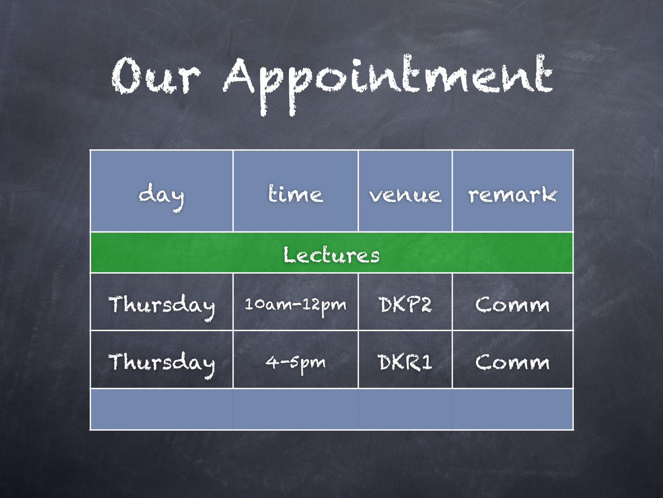
Our Appointment
day time venue remark
Lectures
Thursday 10am-12pm DKP2 Comm
Thursday 4-5pm DKR1 Comm
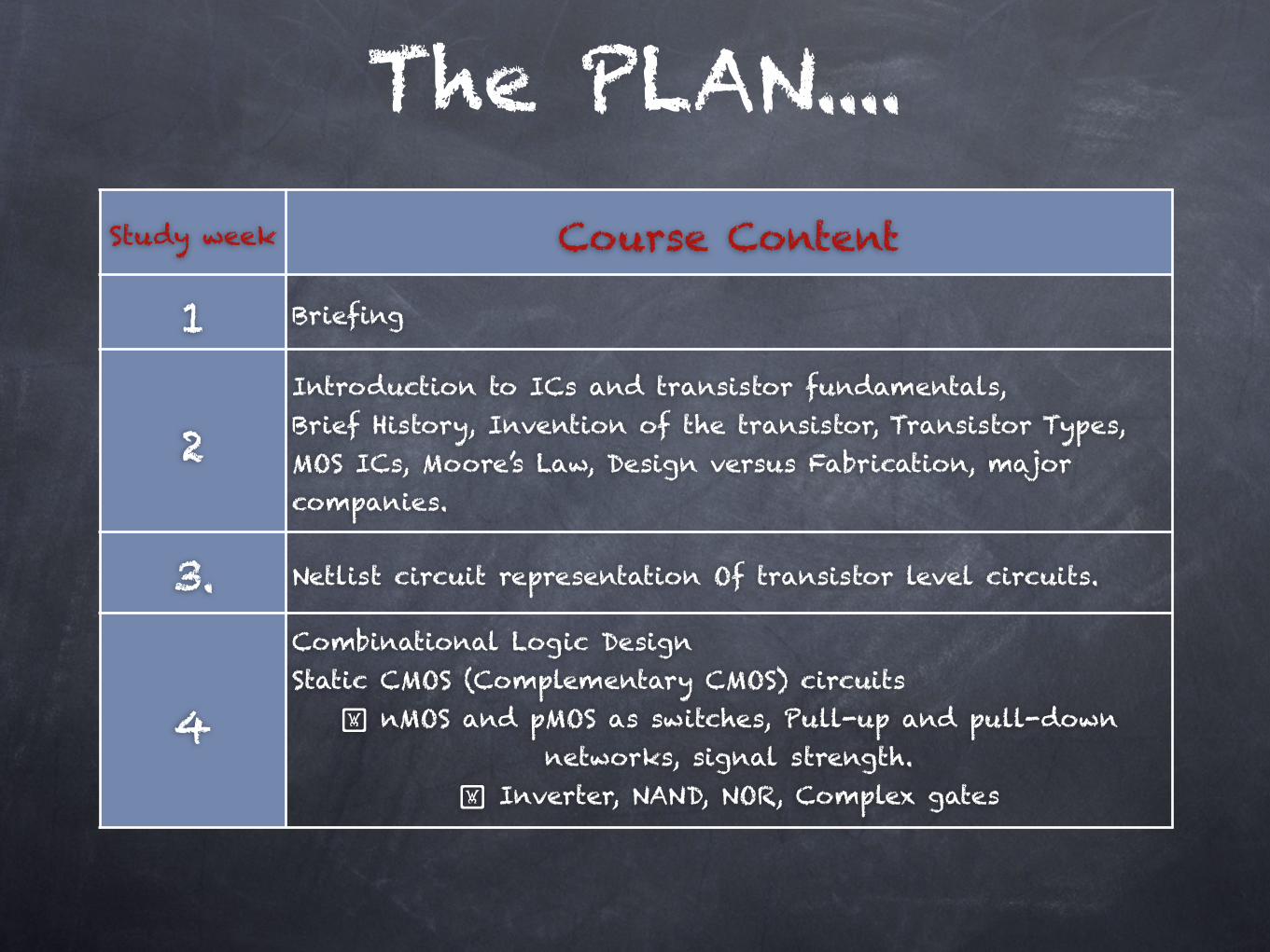
The PLAN....Study week Course Content
1 Briefing
2Introduction to ICs and transistor fundamentals, !Brief History, Invention of the transistor, Transistor Types, MOS ICs, Moore’s Law, Design versus Fabrication, major companies.
3. Netlist
Netlist circuit representation Of transistor level circuits.
4
Combinational Logic Design!Static CMOS (Complementary CMOS) circuits!! nMOS and pMOS as switches, Pull-up and pull-down
networks, signal strength.!! Inverter, NAND, NOR, Complex gates!
!
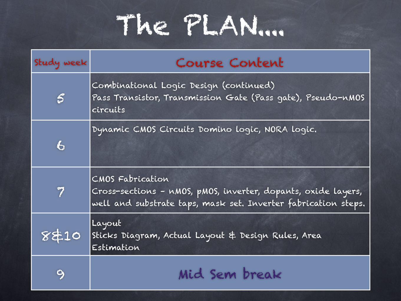
The PLAN....Study week Course Content
5Combinational Logic Design (continued)!Pass Transistor, Transmission Gate (Pass gate), Pseudo-nMOS circuits
6Dynamic CMOS Circuits Domino logic, NORA logic.!!
7CMOS Fabrication!Cross-sections – nMOS, pMOS, inverter, dopants, oxide layers, well and substrate taps, mask set. Inverter fabrication steps.
8&10Layout!Sticks Diagram, Actual Layout & Design Rules, Area Estimation
9 Mid Sem break
The PLAN....Study week Course Content
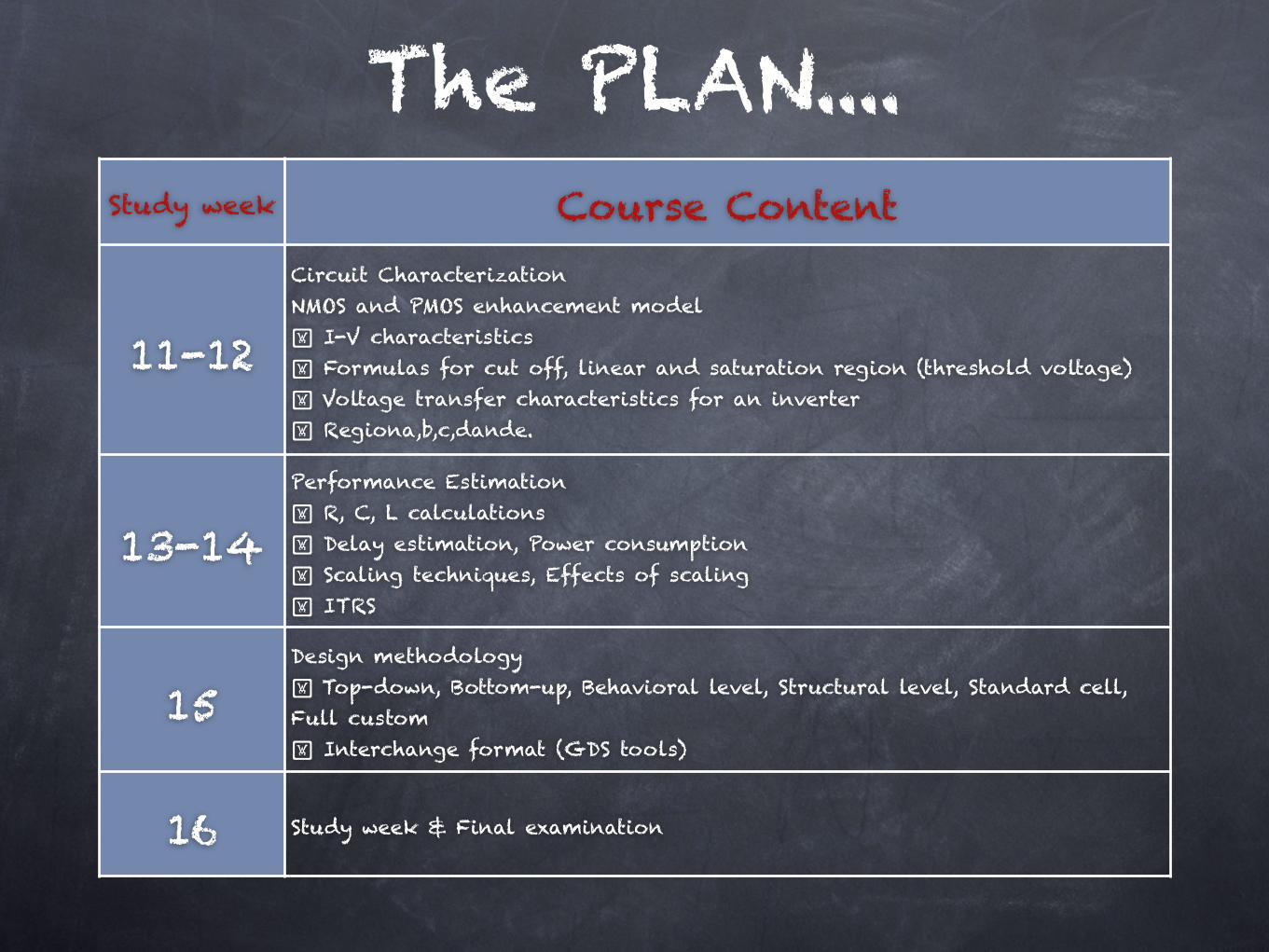
11-12
Circuit Characterization!NMOS and PMOS enhancement model!! I-V characteristics!! Formulas for cut off, linear and saturation region (threshold voltage)!! Voltage transfer characteristics for an inverter!! Regiona,b,c,dande.
13-14Performance Estimation!! R, C, L calculations!! Delay estimation, Power consumption!! Scaling techniques, Effects of scaling!! ITRS
15Design methodology!! Top-down, Bottom-up, Behavioral level, Structural level, Standard cell, Full custom!! Interchange format (GDS tools)
16 Study week & Final examination
Text book
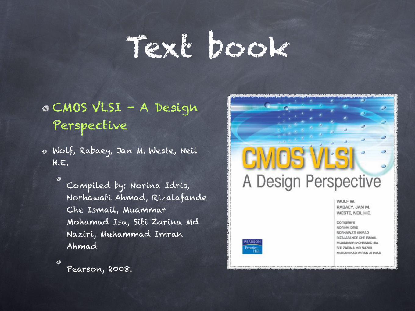
CMOS VLSI - A Design Perspective!
Wolf, Rabaey, Jan M. Weste, Neil H.E. !
Compiled by: Norina Idris, Norhawati Ahmad, Rizalafande Che Ismail, Muammar Mohamad Isa, Siti Zarina Md Naziri, Muhammad Imran Ahmad !
Pearson, 2008.
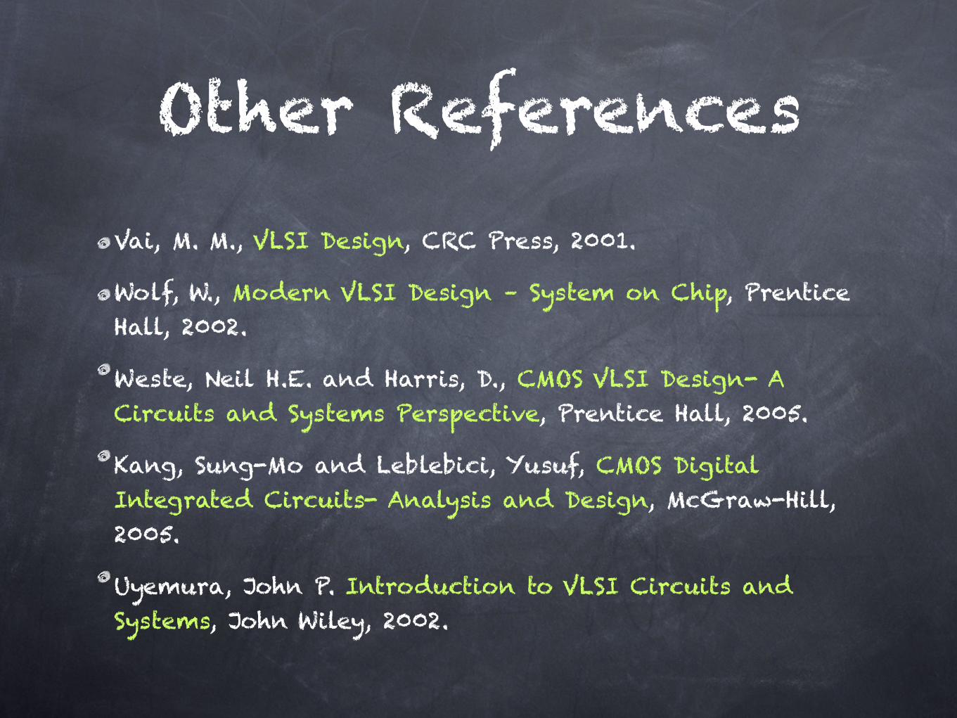
Other ReferencesVai, M. M., VLSI Design, CRC Press, 2001. !
Wolf, W., Modern VLSI Design – System on Chip, Prentice Hall, 2002. !
Weste, Neil H.E. and Harris, D., CMOS VLSI Design- A Circuits and Systems Perspective, Prentice Hall, 2005. !
Kang, Sung-Mo and Leblebici, Yusuf, CMOS Digital Integrated Circuits- Analysis and Design, McGraw-Hill, 2005. !
Uyemura, John P. Introduction to VLSI Circuits and Systems, John Wiley, 2002.

What is IC???
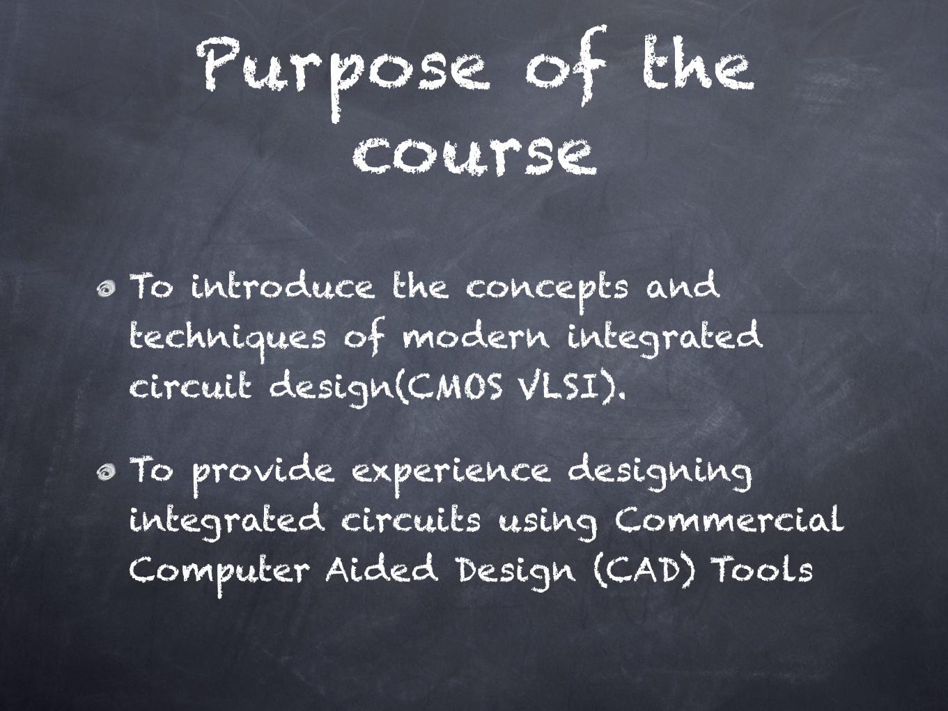
Purpose of the course
To introduce the concepts and techniques of modern integrated circuit design(CMOS VLSI).!
To provide experience designing integrated circuits using Commercial Computer Aided Design (CAD) Tools
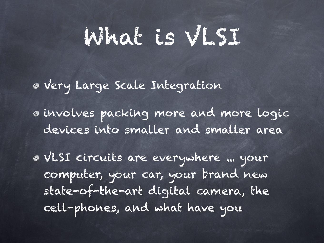
What is VLSI
Very Large Scale Integration!
involves packing more and more logic devices into smaller and smaller area!
VLSI circuits are everywhere ... your computer, your car, your brand new state-of-the-art digital camera, the cell-phones, and what have you
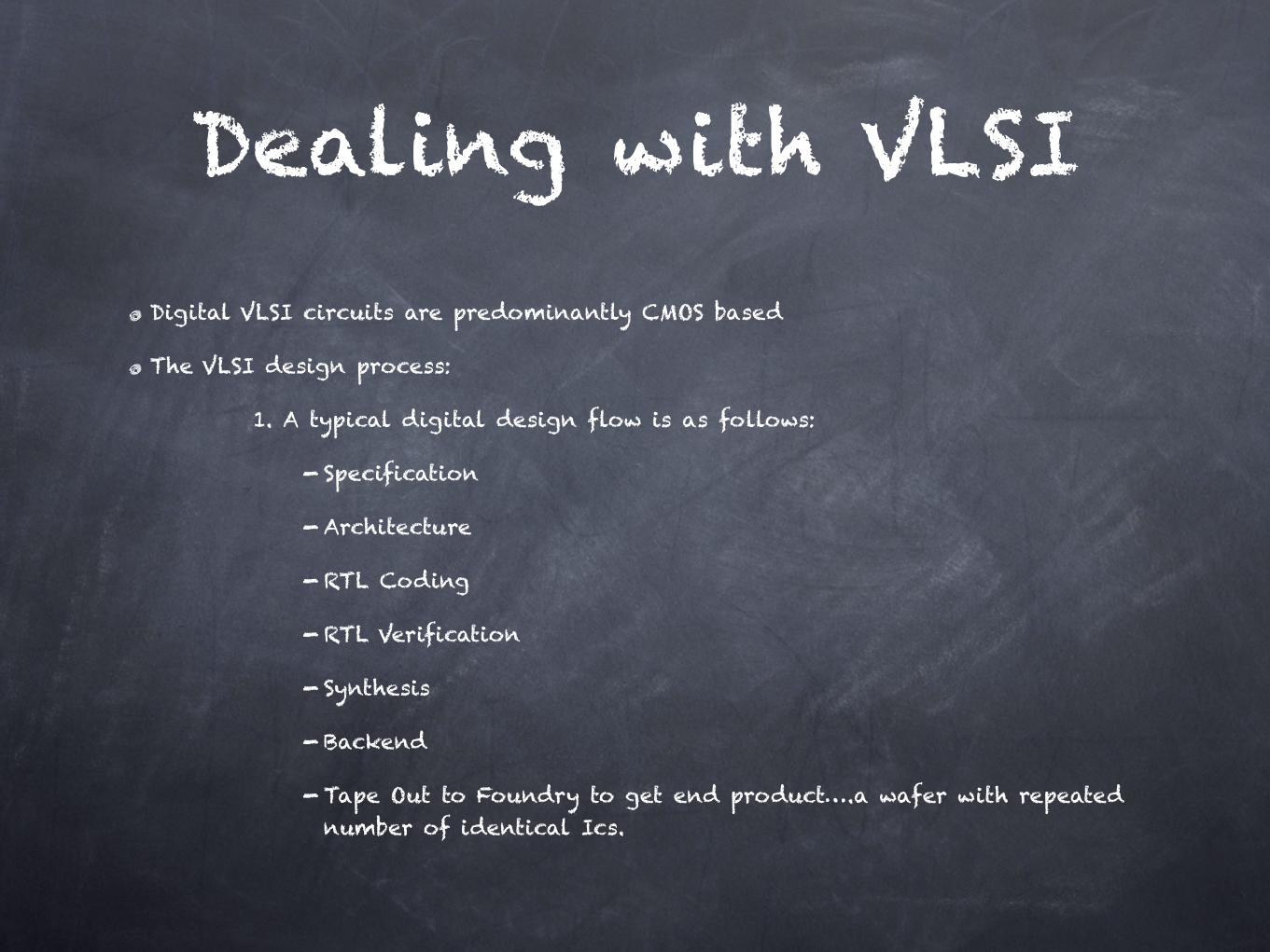
Dealing with VLSIDigital VLSI circuits are predominantly CMOS based!
The VLSI design process:!
1. A typical digital design flow is as follows:!
- Specification !
-Architecture !
-RTL Coding !
-RTL Verification !
- Synthesis !
- Backend !
-Tape Out to Foundry to get end product….a wafer with repeated number of identical Ics.