enee482-dr. zaki1 impedance matching with lumped elements ylyl jx 1 jb 2
Post on 21-Dec-2015
229 views
TRANSCRIPT

ENEE482-Dr. Zaki 1
Impedance Matching with Lumped Elements
1G when usedCircuit L YL
jX1
jB2
LL
L
LL
LLLLL
LLL
LLL
LLL
in
RB
Z
R
ZX
BX
XR
RZXRZRXB
XRZBXBX
ZRZXRXB
Z
jXRjB
jX
ZjB
jXZ
2
00
21
220
220
2
0221
0012
0
2
1
2
1
1
/
)1(
)(
11
11

ENEE482-Dr. Zaki 2
jB2
jX1
ZL
1R when usedCircuit L
0
02
01
022
0102
01
2
/)(
)(
)(
)(
/1)(
1
Z
RRZB
XRZRX
RZBXX
RZXXZB
ZXXjR
jBY
LL
LLL
LL
LL
LLin

ENEE482-Dr. Zaki 3
Single-Stub Matching
Load impedance jBYin 1
1tan
2length stub The
1
1cos
4
1
epoint wher minimum- voltage thefrom distance thebe Let
real ist coefficien reflection then thereal, is If1
1
10
10
0
S
S
S
Sd
jBY
d
Y
SY
in
L
in
Input admittance=S

ENEE482-Dr. Zaki 4
Series Stub
Input impedance=1/S
Voltage minimum
S
S
Xjj
dS
X
S
Sd
djjS
djSXjZ
SZ
in
in
1tan
2
tan
tan)1
1(
1
1cos
4
tan1
tan1
/1
10
0
0
10
01
01

ENEE482-Dr. Zaki 5
Double Stub Matching Network
jB1jB2YL
ab
2
1
P tocircle econductancconstant along
point themoves which Bj esusceptanc a adds stubfirst The
aa plane at the
into ed transformis
LLL
LL
BjGY
YY
b a

ENEE482-Dr. Zaki 6
0
r=1
x=1
x=-1
Real part ofRefl. Coeff.
Pshort circuit Popen circuit
r=0.5
Smith Chart
YL
. cancel willstub The circle. 1G on the liemust P The
.Y is admittanceinput theb-b plane At the
d2
anglean through circle radiusconstant a along P toP from Move
3
b
32
b
bb
Bj
BjG

ENEE482-Dr. Zaki 7
0
r=1
x=1
x=-1
Real part ofRefl. Coeff.
Pshort circuit Popen circuit
r=0.5
Smith Chart
YL
Rotate the the G=1 circle through an angle -The intersection of G=1 and the GL circle determine
The point P2
P2
P3
G1=1

ENEE482-Dr. Zaki 8
0
r=1
x=1
x=-1
Real part ofRefl. Coeff.
Pshort circuit Popen circuit
r=0.5
Smith Chart
YL
The shaded range is for the load impedance whichcannot be matched when d=1/8 wavelength

ENEE482-Dr. Zaki 9
Quarter-Wave Transformers
ZL
4
ZC=Z0 ZC=Z1
LL
L
in
in
L
L
L
LL
Lin
ZZjtZZ
ZZ
ZZ
ZZ
fttjZZ
tjZZZ
ZZZ
ZZ
Z
jZZ
jZZZZ
00
0
0
0
1
11in
01
0
21
1
11
2
)(tantan , Z
matchperfect
)4/tan(
)4/tan(

ENEE482-Dr. Zaki 10
small very is )(f2f width band The
1)(
2cos
is of valueingcorrespond The
toleratedbecan that
t coefficien reflection of valuemaximum theis If
cos2
1sec and /2 then fnear is f If
sec2
1
1
0
21
11
m
m
1
1
20
2
1
1
m
mL
Lmm
L
L
L
L
f
ZZ
ZZ
ZZ
ZZ
ZZ
ZZ

ENEE482-Dr. Zaki 11
m
2
m
Bandwidth characteristic for a singleSection quarter wave transformer
m2
2Bandwidth

ENEE482-Dr. Zaki 12
Theory of Small Reflection
2
23
12
112
12
2121
1212
121
2
, 2
1
,
ZZ
ZZ
ZZ
ZT
ZZ
ZT
ZZ
ZZ
L
L
L1
2
1

ENEE482-Dr. Zaki 13
unity tocompared small are and If
1
1 , 11for Substitute
1
...
31
2312
31
231
1211212
232
232112
12
30
22
321121
42
232112
2321121
jj
j
j
jjnn
n
nj
jj
ee
e
TT
e
eTTeeTT
eTTeTT
1 3
21T je

ENEE482-Dr. Zaki 14
1 21
jeTT 232112
jeTT 4232112
jeTT 623
222112
jeT 2321
jeT 423212
jeT 623
2221
jeT 23221
jeT 423
2221
Multiple reflection of waves for a circuitwith two reflection junctions

ENEE482-Dr. Zaki 15
Approximate Theory for Multi-Section Quarter Wave Transformers
L
021 N
A multi-section quarter-wave transformer
NNL
NLN
nnn
nnn
L
ZZ
ZZ
ZZ
ZZ
ZZ
ZZ
Z
ist coefficien reflectionlast The
,
real is Assume
1
10
01
010

ENEE482-Dr. Zaki 16
even Nfor ]cos
...)cos(...)2cos(cos[2
odd Nfor ]cos
...)2cos(...)2cos(cos[2
...])()([
...etc , , ,
i.e. lsymmetrica isr tranforme that theAssume
....
2/)(
10
2/)1(
10
)2()2(10
22110
242
210
N
njN
N
njN
NjNjjNjNjN
NNN
jNN
jj
nNNNe
nNNNe
eeeee
eee

ENEE482-Dr. Zaki 17
Binomial Transformer
0L
0L
0
n
2j-
0
Z
Z)0( , or 0when
/4for which ffrequency center the toscorrespond /2
1-N1,2,...,nfor /2at 00/)(d
and /2for 0)( that Note
)(cos2
)(
)eA(1)( Choose
/2. wherefrequency matching
at the vanish )or (frequency w.r.t sderivative 1-Nfirst theand
if obtained is sticscharacteri passbandflat maximally A
Z
Z
d
A
eeeA
f
n
NN
NjjNj
N

ENEE482-Dr. Zaki 18
nNNn
L
LNn
jNN
jjjn
NN
NNNnN
Nn
CZZ
ZZ
eeee
CNCCCC
0
0
242
210
2N
0n
Nn
110
2
....CA)(
:bygiven
response actual the toresponse passband desired theEquate
..... , 1, ,
!)!(
!
!
)1)...(2)(1(
Z
Z2)1(
Z
Z2)(
Z
Z2A , 2)0(
2
00L
0L2
0L
0L
0L
0L
nnN
N
n
nNNNNC
eCZ
Ze
Z
Z
Z
ZA
Nn
jN
n
Nn
NNjN
NN

ENEE482-Dr. Zaki 19
01
2
0
1
1
2
0
1
0
)1(
00
01
21
1
11
nn
ln2
1)...ln(
2
1
ln...lnln2
1)0(2
)ln(2
ln2]2[22ln
ln2
1
thefrom found becan Zimpedances sticcharacteri The
Z
Z
Z
Z
Z
Z
Z
Z
Z
Z
Z
Z
Z
ZA
Z
ZA
Z
ZCC
ZZ
ZZ
Z
Z
eZZ
ZZ
ZZ
Z
Z
L
N
L
N
LN
LN
LNn
NNn
L
LNn
n
n
nn
nnn
nn
n
n
n
1
12l : Use
x
xnx

ENEE482-Dr. Zaki 20
N
mmm
N
m
m
mNN
m
Af
ff
A
A
/1
1
0
0
0
/1
1m
2
1cos
42
42
)(2
f
f
:isbandwidth fractional The
2
1cos
passband theof edgelower theis 2/
cos2
is passband over the
toleratedbecan that coeficient reflection of valuemaximum The

ENEE482-Dr. Zaki 21
Example
ZLZ2Z1Z0
Z3
Design a three section binomial transformer to match a 50 Ohms load to a 100 Ohms line. Calculate the bandwidthFor max reflection =.05 over the passband.
1!3)!33(
!3 ,3
!2)!23(
!3
, 3!1)!13(
!3 , 1
!0)!03(
!3
ln2
12
100 Z,50 Z3,N sections 3For
33
32
31
30
04
0
03
0L
CC
CC
Z
Z
ZZ
ZZA L
L
L

ENEE482-Dr. Zaki 22
5.5400.4100
50ln)3(27.70lnln
ln2lnlnZ :2
7.7026.4100
50ln)3(27.91lnln
ln2lnlnZ :1
7.91518.4100
50ln2100lnln
ln2lnlnZ :0
33
3
0
32
323
23
2
0
31
312
13
1
0
30
301
ZZ
Z
ZCZn
ZZ
Z
ZCZn
ZZ
Z
ZCZn
L
L
L

ENEE482-Dr. Zaki 23
Chebyshev Transformer
nT
xTxxTxT
xxxT
xxT
xxT
xT
n
nnn
n
cos)(cos
)()(2)(
34)(
12)(
)(
n degree of polynomial Chebyshev :)(
21
33
22
1
m
m
0
0
ZZ
ZZ
L
L
m

ENEE482-Dr. Zaki 24
)(sec T
)cos(sec T
Z
Zln
2
1
)(sec T2
)/ln(
ln2
1)(sec TA
Z
Z
: have we0When
)cos(sec T A
.......] )2cos(
....)2cos(cos[2
cos
coscoscos
cos
cos Consider
mN
mN
0
L
mN
0
0mN
0L
0L
mN
10
1
jN
L
L
jN
n
jN
mmn
e
ZZA
Z
Z
Z
Z
e
nN
NNe
nT

ENEE482-Dr. Zaki 25
)12(cossec4)34cos2cos4(sec)cos(secT
cossec3)3coscos3(sec)cos(sec T
1)2cos1(sec1)cossec(2)cos(sec T
cossec)cos(sec T
....])2cos(.......)2cos(cos[2
2)1(2)(cos
2
)/ln(cos
1cossec , )/ln(
2
1)(sec T
)(sec T2
)/ln(
unity is )cos(sec T of valuemaximum thepassband In the
2m
4m4
m3
m3
22mm2
mm1
101
2
0
2
01m0
1mN
mN
0
mN
mm
mm
m
nm
nnn
jmn
m
nm
jnnnjjnnn
m
LLm
Lm
mnCnCnC
eCeee
ZZ
NZZ
ZZ
ENEE482-Dr. Zaki 26
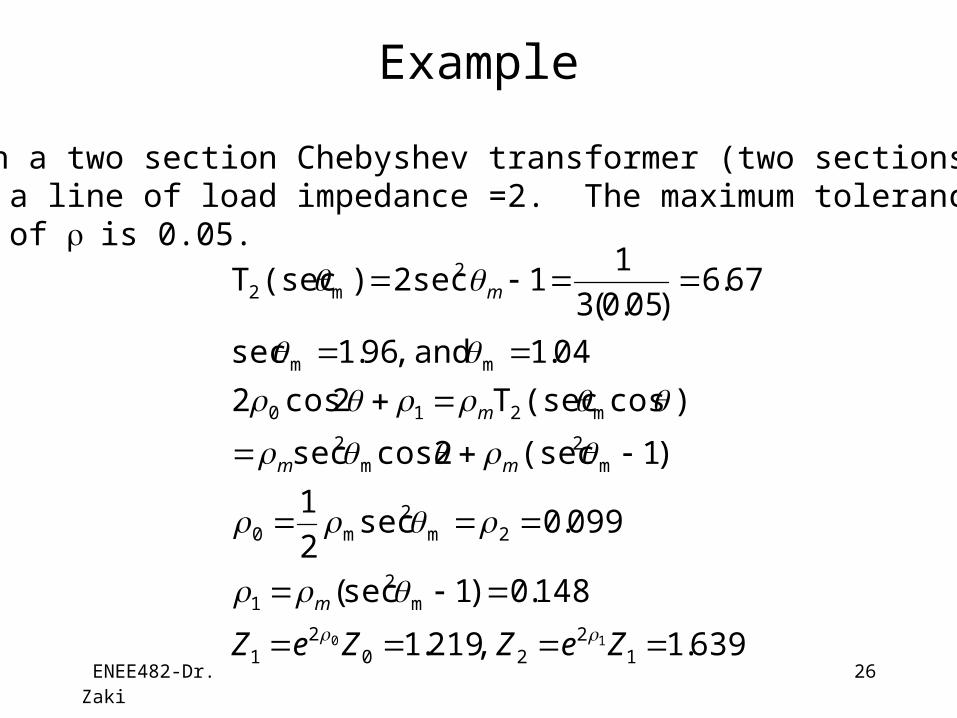
Example
Design a two section Chebyshev transformer (two sections) toMatch a line of load impedance =2. The maximum tolerance Value of is 0.05.
639.1 ,219.1
148.0)1sec(
099.0sec2
1
)1(seccos2sec
)cos(secT2cos2
04.1 and ,96.1sec
67.6)05.0(3
11sec2)(secT
12
202
1
m2
1
2m2
m0
m2
m2
m210
mm
2m2
10
ZeZZeZ
m
mm
m
m

ENEE482-Dr. Zaki 27

ENEE482-Dr. Zaki 28
Design of Complex Impedance Termination
Amplifier ZcZc
Input Matchingnetwork
Output Matchingnetwork
ZsZL
Microwave amplifier circuit

ENEE482-Dr. Zaki 29
MM
PMR
V
ZZ
RR
R
VR
jXRZ
R
V
L
inLT
c
LT
LT
T
cL
TTT
T
c
42
14
42
1 todeliveredpower The
42
1 :isnetwork thefrompower available The
2
0
2
2
0
2
0

ENEE482-Dr. Zaki 30
jB1
Stub
ZL ZcZL
l l
G=1
jB1ZL G=1jB2ZL G=1
jX1 jX2
=
Transmission Line Matching Network
Alternative Matching Networks

ENEE482-Dr. Zaki 31
Gen
erat
or
Load
l/ =
0.43
75l/ = 0.0626j1
-j1
YL
ZL= 0.4-j0.2
Y’in1
2
G=1
G=2
Y”in
Design Procedure for the Matching Network with Shunt Stub

ENEE482-Dr. Zaki 32
Impedance Mismatch Factor
factormismatch impedance thecalled is 4
4
42
1
42
1
obtained ispower available Maximum
X , then ZIf
2
1
2
2
2
2
in*
in
2
Sin
Sin
ava
Sin
Sin
S
Sin
S
Sava
SSinS
ininS
Sin
inS
S
ZZ
RRM
MPZZ
RR
R
VP
R
VP
XRRZ
RZZ
VP
ZZ
VI

ENEE482-Dr. Zaki 33
Z11-Z12Z22-Z12
Z12
ZL
ZS
VS
Zin
ZT
Voc
ZL
ML
A T matching network Thevenin equivalentnetwork
2122211
11
22T
11
12 Z,
ZZZ
ZZ
ZZ
ZZ
VZV
S
S
S
Soc

ENEE482-Dr. Zaki 34
Impedance Transformation and MatchingReview of Transmission Lines and Smith Chart
0
0
0
0
0
0
00
0
0
0
00
00
TCOEFFICEIN REFLECTION
I(z)
T.L. theof Impedance ticCharacters :
,)()()(
)()()(
V
V
eZ
Ve
Z
V
ZI
V
I
V
eIeIzIzIzI
eVeVzVzVzV
zz
zz
zz
Zg
ZL
Z0Vg
Finite Transmission Line terminated with load impedance
Z=LZ=0
L

ENEE482-Dr. Zaki 35
LZZ
LZZZLzZ
zZZ
zZZZ
zI
zVzZ
zZzZZ
IzI
zZzZIzV
zLz
eZZeZZZ
IzI
eZZeZZI
zV
eZIVVeZIVV
eZ
Ve
Z
VIeVeVV
L
Lin
L
L
LL
LL
zLL
zLL
L
zLL
zLL
L
LLL
LLL
LLL
LLL
tanh
tanh)(
tanh
tanh
)(
)()(
)coshsinh()(
)sinhcosh()(
Let
])()[(2
)(
])()[(2
)(
)(2
1 )(
2
1
, ,
0
00
0
00
00
0
)(0
)(0
0
)(0
)(0
0000
0
0
0
000

ENEE482-Dr. Zaki 36
Standing wave ration (SWR) S:
1S
1-S ;
1
1
min
max
V
VS
Smith Chart:
jjL
jjL
jL
jLin
in
j
j
LL
Lir
L
LL
L
L
L
L
L
L
L
e
e
e
e
Z
ZZ
e
ez
z
z
jxrZ
Z
eZZ
ZZ
2
2
2
2
0
0L
L
0
0
1
1
1
1
)(1
)(1
1
1 ;
1
1
1
1z
z impedance normalized The

ENEE482-Dr. Zaki 37
x
xxx
r
r
rrr
r
xr
j
jjxr
ir
ir
ir
ir
ir
i
ir
ir
ir
ir
1 and 1at centered and
1 radius of circle a ofEquation ;
11)1(
0 and 1
at centered and
1
1 radius a of circle a ofEquation ;
1
1)
1(
)1(
2 ;
)1(
1
)1(
)1(
222
222
2222
22

ENEE482-Dr. Zaki 38
Imaginary part ofRefl. Coeff.
0
r=1
x=1
x=-1
Real part ofRefl. Coeff.
Pshort circuit
Popen circuit
r=0.5
Smith Chart

ENEE482-Dr. Zaki 39
Review of Transmission Lines and Smith Chart
0
0
0
0
0
0
00
0
0
0
00
00
TCOEFFICEIN REFLECTION
I(z)
T.L. theof Impedance ticCharacters :
,)()()(
)()()(
V
V
eZ
Ve
Z
V
ZI
V
I
V
eIeIzIzIzI
eVeVzVzVzV
zz
zz
zz
Zg
ZL
Z0Vg
Finite Transmission Line terminated with load impedance
Z=LZ=0
L