energy efficiency analysis and implementation of …cgebotys/new/kenney_david.pdf · energy...
TRANSCRIPT

Energy Efficiency Analysis and
Implementation of AES on an FPGA
by
David Kenney
A thesis
presented to the University of Waterloo
in fulfillment of the
thesis requirement for the degree of
Master of Applied Science
in
Electrical and Computer Engineering
Waterloo, Ontario, Canada, 2008
©David Kenney 2008

ii
AUTHOR'S DECLARATION
I hereby declare that I am the sole author of this thesis. This is a true copy of the thesis, including any
required final revisions, as accepted by my examiners.
I understand that my thesis may be made electronically available to the public.

iii
Abstract
The Advanced Encryption Standard (AES) was developed by Joan Daemen and Vincent Rjimen and
endorsed by the National Institute of Standards and Technology in 2001. It was designed to replace
the aging Data Encryption Standard (DES) and be useful for a wide range of applications with
varying throughput, area, power dissipation and energy consumption requirements.
Field Programmable Gate Arrays (FPGAs) are flexible and reconfigurable integrated circuits that
are useful for many different applications including the implementation of AES. Though they are
highly flexible, FPGAs are often less efficient than Application Specific Integrated Circuits (ASICs);
they tend to operate slower, take up more space and dissipate more power. There have been many
FPGA AES implementations that focus on obtaining high throughput or low area usage, but very little
research done in the area of low power or energy efficient FPGA based AES; in fact, it is rare for
estimates on power dissipation to be made at all.
This thesis presents a methodology to evaluate the energy efficiency of FPGA based AES designs
and proposes a novel FPGA AES implementation which is highly flexible and energy efficient. The
proposed methodology is implemented as part of a novel scripting tool, the AES Energy Analyzer,
which is able to fully characterize the power dissipation and energy efficiency of FPGA based AES
designs. Additionally, this thesis introduces a new FPGA power reduction technique called
Opportunistic Combinational Operand Gating (OCOG) which is used in the proposed energy efficient
implementation.
The AES Energy Analyzer was able to estimate the power dissipation and energy efficiency of the
proposed AES design during its most commonly performed operations. It was found that the
proposed implementation consumes less energy per operation than any previous FPGA based AES
implementations that included power estimations. Finally, the use of Opportunistic Combinational
Operand Gating on an AES cipher was found to reduce its dynamic power consumption by up to 17%
when compared to an identical design that did not employ the technique.

iv
Acknowledgements
I would like to thank my supervisor Dr. Catherine Gebotys, for all her support, advice and
encouragement over throughout this thesis. Additionally, I would also like to my parents, Doug and
Cheryl Kenney, as well Rachel Morrison for all of their kindness, support and encouragement.
I also greatly appreciate the funding that was made available to me for this research by the Natural
Sciences and Engineering Research Council of Canada (NSERC) as well as the University of
Waterloo and the Electrical and Computer Engineering at the University of Waterloo.

v
Table of Contents
List of Figures ..................................................................................................................................... viii
List of Tables .......................................................................................................................................... x
Chapter 1 Introduction ............................................................................................................................ 1
1.1 Motivation .................................................................................................................................... 1
1.2 Contributions of This Thesis ........................................................................................................ 2
1.3 Thesis Outline ............................................................................................................................... 2
Chapter 2 Background ............................................................................................................................ 4
2.1 Advanced Encryption Standard .................................................................................................... 4
2.1.1 Overview ............................................................................................................................... 4
2.1.2 SubBytes ................................................................................................................................ 6
2.1.3 ShiftRows .............................................................................................................................. 8
2.1.4 MixColumns .......................................................................................................................... 9
2.1.5 AddRoundKey ..................................................................................................................... 10
2.1.6 Key Expansion..................................................................................................................... 10
2.1.7 Equivalent Inverse Cipher ................................................................................................... 11
2.1.8 Composite Fields SubBytes ................................................................................................. 13
2.2 Field Programmable Gate Arrays ............................................................................................... 15
2.2.1 Altera Cyclone II ................................................................................................................. 16
2.3 Power and Energy Analysis........................................................................................................ 18
2.3.1 Power Usage in FPGAs ....................................................................................................... 19
2.4 FPGA Design and Analysis Tools .............................................................................................. 20
2.4.1 Altera Quartus II Design and Analysis Tools ...................................................................... 22
2.5 Chapter Summary ....................................................................................................................... 24
Chapter 3 Related Work ....................................................................................................................... 25
3.1 Low Power FPGA Design Methodologies ................................................................................. 25
3.2 High Throughput FPGA Based AES Implementations .............................................................. 27
3.3 Low Area FPGA Based AES Implementations .......................................................................... 27
3.4 Low Power FPGA Based AES Implementations ....................................................................... 27
3.5 Chapter Summary ....................................................................................................................... 29
Chapter 4 Design Methodology............................................................................................................ 30
4.1 Design Goals .............................................................................................................................. 30

vi
4.2 Energy Efficiency Design Strategies ......................................................................................... 30
4.2.1 Pipelining ............................................................................................................................ 31
4.2.2 Use of Embedded Block RAM Components ...................................................................... 32
4.2.3 Economic Key Expansion ................................................................................................... 32
4.2.4 Register Clock Enable Gating ............................................................................................. 33
4.2.5 Opportunistic Combinational Operand Gating ................................................................... 35
4.3 Methodology to Develop a High Energy Efficiency Full AES Design ..................................... 37
4.4 Chapter Summary ...................................................................................................................... 37
Chapter 5 Advanced Encryption Standard Designs ............................................................................. 38
5.1 Balanced AES Round Structure ................................................................................................. 38
5.2 S-Box Architectures ................................................................................................................... 39
5.2.1 Logic Based Composite Field S-Box Architecture ............................................................. 40
5.2.2 Pipelined Logic Based Composite Field S-Box Architecture ............................................. 41
5.2.3 Opportunistically Gated Composite Fields S-Box Design .................................................. 42
5.2.4 Memory Based S-Box Design ............................................................................................. 47
5.3 MixColumns Designs ................................................................................................................. 48
5.3.1 Logic Based MixColumns Design ...................................................................................... 48
5.3.2 Pipelined Logic Based MixColumns Design ...................................................................... 50
5.3.3 Opportunistically Gated MixColumns Design .................................................................... 51
5.4 AES Cipher Designs .................................................................................................................. 52
5.4.1 Basic Logic Cipher.............................................................................................................. 52
5.4.2 Piped Logic Cipher ............................................................................................................. 56
5.4.3 OCOG Logic Cipher ........................................................................................................... 59
5.4.4 Basic Memory Based Cipher .............................................................................................. 59
5.4.5 Enhanced Memory Based Cipher........................................................................................ 62
5.5 Full AES with Key Expansion Design ....................................................................................... 65
5.5.1 Application of Economic Key Expansion ........................................................................... 65
5.5.2 Full AES Key Expander Design ......................................................................................... 66
5.5.3 Full AES Cipher Design ..................................................................................................... 70
5.6 Chapter Summary ...................................................................................................................... 75
Chapter 6 Energy Analysis Methodology ............................................................................................ 76
6.1 Analysis Objectives ................................................................................................................... 76
vii
6.1.1 Operations Assessed for Power Dissipation and Energy Efficiency ................................... 77
6.2 Methodology to Assess Energy Efficiency and Power Consumption ........................................ 78
6.3 AES Energy Efficiency Analyzer Script .................................................................................... 79
6.3.1 Operational Flow of Script .................................................................................................. 79
6.3.2 Project Setup ........................................................................................................................ 80
6.3.3 Compilation ......................................................................................................................... 81
6.3.4 Operation Simulation ........................................................................................................... 83
6.3.5 Design Analysis ................................................................................................................... 86
6.4 Chapter Summary ....................................................................................................................... 87
Chapter 7 Experimental Results and Discussion .................................................................................. 88
7.1 Cipher Designs ........................................................................................................................... 88
7.1.1 Resource Usage and Performance of AES Ciphers ............................................................. 89
7.1.2 Power Dissipation of AES Ciphers ..................................................................................... 90
7.1.3 Energy Efficiency of AES Ciphers ...................................................................................... 91
7.2 Energy Efficient Full AES Design ............................................................................................. 92
7.2.1 Resource Utilization and Performance of Full AES Design ............................................... 92
7.2.2 Power Dissipation of Full AES Design ............................................................................... 93
7.2.3 Energy Efficiency of Full AES Design ............................................................................... 94
7.2.4 Effect of Varying Frequency on Energy Efficiency ............................................................ 96
7.3 Comparison to Previous Research .............................................................................................. 97
7.3.1 Resource Utilization and Performance of Compared AES Designs .................................... 98
7.3.2 Energy Efficiency of Compared AES Designs .................................................................. 100
7.4 Discussion and Analysis ........................................................................................................... 102
7.4.1 The AES Energy Analyzer ................................................................................................ 102
7.4.2 Energy Efficiency Strategies in AES................................................................................. 103
7.4.3 The Full Energy Efficient AES Implementation ............................................................... 104
7.5 Chapter Summary ..................................................................................................................... 104
Chapter 8 Conclusions ........................................................................................................................ 106
8.1 Summary and Contributions ..................................................................................................... 106
8.2 Future Work ............................................................................................................................. 106
Appendix A Glossary of Acronyms ................................................................................................... 108
Bibliography ....................................................................................................................................... 110

viii
List of Figures
Figure 1: Standard AES Round Structure ............................................................................................. 5
Figure 2: AES State Array [7]............................................................................................................... 6
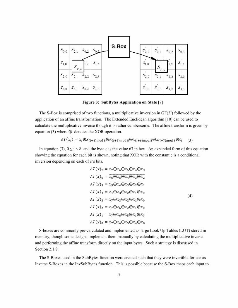
Figure 3: SubBytes Application on State [7] ........................................................................................ 7
Figure 4: ShiftRows Application on State [7] ....................................................................................... 8
Figure 5: InvShiftRows Application on State [7] ................................................................................. 9
Figure 6: AES Key Expansion ............................................................................................................. 11
Figure 7: Standard AES Round Structure with Equivalent Inverse Cipher ........................................ 12
Figure 8: Composite Fields Multiplicative Inversion ......................................................................... 14
Figure 9: Cyclone II Logic Element [17] ............................................................................................ 17
Figure 10: Cyclone II Block RAM [17] .............................................................................................. 17
Figure 11: Cyclone II Routing Resources [17] ................................................................................... 18
Figure 12: Cyclone II Average Dynamic Power Dissipation [21] ...................................................... 20
Figure 13: Power Aware Memory Synthesis [21] .............................................................................. 23
Figure 14: Iterative Pipeline Structure ................................................................................................ 31
Figure 15: Single Valid Data Propagation in Iterative Pipeline Structure .......................................... 34
Figure 16: Opportunistic Combinational Operand Gating Example ................................................... 36
Figure 17: Balanced AES Round Structure ........................................................................................ 39
Figure 18: Combined Affine and Isomorphic Mapping Composite Field S-Box ............................... 40
Figure 19: No Cut Composite Fields S-Box ....................................................................................... 41
Figure 20: Six Cut Composite Fields S-Box ....................................................................................... 42
Figure 21: Pre Multiplicative Inverse Technology Map ..................................................................... 43
Figure 22: Potential LUTs to Gate in the Pre Multiplicative Inverse Technology Map ..................... 44
Figure 23: Memory Based S-Box Implementation ............................................................................. 47
Figure 24: No Cut Substructure Sharing MixColumns ....................................................................... 50
Figure 25: One Cut Substructure Sharing MixColumns ..................................................................... 51
Figure 26: Opportunistically Gated One Cut Substructure Sharing MixColumns .............................. 52
Figure 27: Basic General Purpose Logic Cipher ................................................................................ 53
Figure 28: Round Finite State Machine .............................................................................................. 54
Figure 29: Composite Fields S-Boxes with ShiftRows....................................................................... 55
Figure 30: Shift Register Key Storage ................................................................................................ 56
Figure 31: Pipelined General Purpose Logic Cipher .......................................................................... 57

ix
Figure 32: Pipelined General Purpose Logic Cipher Control FSM ..................................................... 58
Figure 33: Basic Memory Based Cipher Control FSM ....................................................................... 59
Figure 34: Basic Memory Based Cipher ............................................................................................. 60
Figure 35: Basic Memory Based Cipher Memory Key Storage .......................................................... 62
Figure 36: Initial and Final Key Storage for Memory Based Cipher .................................................. 62
Figure 37: Gated Pipeline Memory Based Cipher Control FSM ........................................................ 63
Figure 38: Enhanced Memory Cipher ................................................................................................. 64
Figure 39: Gated Pipeline Memory Based Cipher Memory Key Storage ........................................... 65
Figure 40: Full AES Operation Concurrency ...................................................................................... 66
Figure 41: Full AES Control FSM ...................................................................................................... 67
Figure 42: Activate Key Expander Input ............................................................................................. 67
Figure 43: Full AES Key Expander ..................................................................................................... 69
Figure 44: Full AES Initial and Final Key Storage ............................................................................. 70
Figure 45: Full AES Cipher ................................................................................................................. 71
Figure 46: Full AES Shift Keys ........................................................................................................... 72
Figure 47: Full AES Memory Key Storage Enable Signals ................................................................ 73
Figure 48: Full AES Key Storage Memory Address Encoding ........................................................... 74
Figure 49: Flow of AES Energy Efficiency Analyzer ......................................................................... 80
Figure 50: Flow of AES Energy Analyzer Compilation ..................................................................... 82
Figure 51: Flow of AES Energy Analyzer Operation Simulation ....................................................... 84
Figure 52: Effect of Varying Frequency on Energy Efficiency ........................................................... 97
x
List of Tables
Table 1: Round Constant Values ........................................................................................................ 10
Table 2: Altera Cyclone II Resources [17] ......................................................................................... 16
Table 3: AES Cipher Resource Usage and Performance .................................................................... 89
Table 4: AES Cipher Power Dissipation at 50 MHz........................................................................... 90
Table 5: AES Cipher Energy Efficiency ............................................................................................. 92
Table 6: Full AES Resource Usage and Performance ........................................................................ 93
Table 7: Full AES Power Dissipation at 50 MHz Under Multi Stream Conditions ........................... 93
Table 8: Full AES Power Dissipation at 50 MHz Under Single Stream Conditions .......................... 94
Table 9: Full AES Energy Efficiency Under Multi Stream Conditions .............................................. 95
Table 10: Full AES Energy Efficiency Under Single Stream Conditions .......................................... 95
Table 11: Effect of Considering Static Power on Energy Efficiency ................................................. 96
Table 12: Comparison AES Resource Usage and Performance ......................................................... 99
Table 13: Comparison AES Normalized Energy Efficiency ............................................................. 101

1
Chapter 1
Introduction
1.1 Motivation
Since its announcement in 2001, the Advanced Encryption Standard (AES) has become a widely
known and relied upon block cipher. It has been used for countless different applications ranging in
size and scale from internet banking operations performed on large web servers [1] to private
communications between a wireless smart card and its reader [2]. Every application has different
requirements such as the speed at which security operations must be performed, the physical area for
embedded hardware, or its power budget. Given this large range of applications and requirements, it
isn‟t surprising that AES designs have been implemented using all sorts of platforms, ranging from
software running on general purpose computer hardware to fully customized hardware platforms
which are able to run much faster, or have a much smaller chip area and power consumption.
Field Programmable Gate Arrays (FPGAs) are a form of customizable hardware platform that is
generally regarded as being much easier to design for than fully customizable hardware is, but unable
to achieve the same level of efficiency in terms of speed, chip area, or power usage as a fully
customized solution. They have been used for many AES implementations, usually attempting to
obtain high speeds for use in server environments that require multiple simultaneous security sessions
or fit in a physically small chip. Though they are usually able to achieve data rates that are high
enough to meet the requirements of many systems, FPGAs are generally regarded as being
unacceptably power hungry for very power constrained environments. In order to counteract FPGA‟s
historically negative reputation with regards to power consumption, FPGA manufacturers have begun
to focus more on the power and energy usage of their products by offering lower power consuming
FPGAs [3] and providing design tools which are useful for estimating and reducing power
consumption [4]. Though FPGAs have a come a long way in terms of improving power
consumption, they still lag behind custom hardware significantly.
In spite of these efforts, FPGAs are still believed to be impractical for AES implementations that
are to be used in an extremely low power environment such a contactless smart card or wireless
sensor network [5]. Regardless, there is no reason why AES cannot be made more energy efficient on
an FPGA platform. There are many large scale server farms that could benefit from more energy
efficient technology to reduce huge electricity costs [6], and mobile electronics which implement
Systems on Chips (SoCs) could benefit from extended battery life. Despite this, there have been very
few attempts to even assess the power consumption or energy efficiency of AES designs on FPGAs
and even fewer attempts to improve its energy efficiency.
2
1.2 Contributions of This Thesis
The main goals of this thesis are to research a thorough and complete methodology to evaluate the
power consumption and energy efficiency of FPGA based AES designs as well as to develop a highly
energy efficient practical AES implementation.
A scripting tool called the AES Energy Analyzer which is capable of completely and thoroughly
assessing the power and energy profile of an FPGA based AES design is presented in this thesis. The
tool takes advantage of a vendor supplied FPGA power estimation tool to develop an energy profile
for the evaluated design based on simulation data, completely automating the analysis process.
Additionally, the tool automates the complex FPGA compilation flow in order to maximize a design‟s
energy efficiency.
A complete and practical energy efficient FPGA based AES implementation is also presented. The
design uses low power and high throughput design techniques to be as energy efficient as possible. It
is also highly flexible and useful for a range of applications including complex multisession or SoC
environments that require moderately high data rates. The power and energy usage of the design is
fully characterized by the AES Energy Analyzer.
Additionally, a novel FPGA specific dynamic power reduction technique called Opportunistic
Combinational Operand Gating (OCOG) is presented. The strategy takes advantage of unused Look
Up Table inputs to reduce signal activity in a design at no additional logic cost. Though only limited
tests have been performed using this technique, initial improvements in dynamic power consumption
of up to 17% above that which is possible through heavy pipelining alone have been observed.
1.3 Thesis Outline
The rest of this thesis is organized as follows: Chapter 2 presents background information on AES,
FPGAs, power and energy analysis, and FPGA design tools which is required for understanding the
rest of the thesis. Chapter 3 discusses related research that has been done in the area of low power
FPGA design techniques as well as FPGA based AES implementations. This chapter also describes
some initial research which has attempted to assess the power consumption of FPGA based AES.
Chapter 4 discusses the methodology used to develop a highly energy efficient AES implementation
and details the low power and high throughput design strategies that are used including OCOG.
Chapter 5 presents the designs which were implemented and evaluated for energy efficiency. This
includes several cipher only designs intended to assess the effectiveness of the design strategies
chosen including OCOGs as well as the proposed energy efficient design. Chapter 6 presents the
power and energy efficiency assessment methodology and fully describes the AES Energy Analyzer
Script. Chapter 7 presents the experimental results obtained by implementing the introduced designs.
This includes a discussion on the effectiveness of the various energy efficiency strategies, and of
course, the energy profile of the proposed full design. This chapter also compares the results obtained

3
in this thesis to previous research which examined FPGA based AES implementations‟ power usage.
Finally, Chapter 8 offers suggestions for future work along with concluding remarks.

4
Chapter 2
Background
This chapter is intended to give background information required for the understanding of the rest of
the thesis. Section 2.1 starts off the chapter with background information on the Advanced
Encryption Standard followed by Section 2.2 which gives background information on Field
Programmable Gate Arrays and introduces the Altera Cyclone II. Section 2.3 introduces the concepts
of power and energy and discusses their analysis in FPGAs. Finally Section 2.4 discusses the FPGA
design and analysis tools used in this thesis.
2.1 Advanced Encryption Standard
The Advanced Encryption Standard is the standard symmetric key block cipher endorsed by the
National Institute of Standards and Technology (NIST) in Federal Information Processing Standard
(FIPS) 197[7]. The standard was published in 2001 by NIST after a four year public competition
which was proposed to find a replacement for the aging Data Encryption Standard (DES). The
Rijndael design submitted by Joan Daemen and Vincent Rjimen won this competition and was
selected as the new Advanced Encryption Standard based on its robust security properties and simple
implementation in both hardware and software [8]. The original Rijndael specification was an
iterative round based cipher which supported block and key sizes of 128, 192 and 256 bytes. The
AES specification is identical to the original except that it limits the block size to 128 bits, retaining
the option of specifying a key size of 128, 192 or 256 bits. The use of larger key sizes increases the
cryptographic strength of the cipher but requires that a greater number of processing rounds be
performed. Currently, 128 bit AES is sufficient for most purposes and is the most commonly used; it
will be the focus of the work done in this thesis. Using a key length of 128 bits requires 10 rounds of
processing.
The remainder of this section is intended to introduce the structure and components of AES.
Section 2.1.1 gives an overview of AES as well as showing its structure. Sections 2.1.2 though 2.1.5
discuss the cipher components of SubBytes, ShiftRows, MixColumns and AddRoundKey, while
Section 2.1.6 discusses the Expand Key function. Section 2.1.7 presents an alternate AES structure
that allows for easier decryption, while Section 2.1.8 introduces a specific method of implementing
the SubBytes Function. For more detailed information on the structure and operation of AES please
see the original NIST FIPS-197 standard [7], or the work of William Stallings [9].
2.1.1 Overview
A full AES implementation can be broken down into two main components: the cipher and the key
expander. The cipher is the component which is responsible for performing encryption or decryption

5
on blocks of input data, while the key expander is responsible for preparing the input key for use by
the cipher in each round. Both encryption and decryption require the cipher to perform 10 rounds of
substitution and permutation operations in order to transform the input data. In order to accomplish
this, encryption uses the SubBytes, ShiftRows, MixColumns, and AddRoundKey functions, while
decryption uses InvSubBytes, InvShiftRows, InvMixColumns and AddRoundKey. The
AddRoundKey function in each round of cipher operation requires the addition of a key which is the
same size as 128 bit block of data. This 128 bit round key must be based on the original 128 bit key
which is supplied along with the data to encrypt or decrypt. The role of the key expander is to
calculate the 128 bit key used in each round based on the original key. A diagram of the operation of
AES can be found in Figure 1.
Figure 1: Standard AES Round Structure
6
As can be seen in Figure 1, the decryption function is the reverse of the encryption function. It
uses the same set of round keys, but in the opposite order, and uses the inverse form of SubBytes,
ShiftRows and MixColumns.
The FIPS defining AES [7] often refers to the 128 bits of data being operated on in the cipher as a 4
byte by 4 byte array called the State. This representation is very useful when describing the operation
of the internal cipher functions and is also used here. An example of the State is pictured in Figure 2
[7]. Each byte of the State is denoted Sr,c, where r and c are the row and column of the byte in the
State.
Figure 2: AES State Array [7]
All of the mathematical operations done in the functions of AES are performed in GF(28). This
means that addition of two bytes can be performed by XORing their corresponding bits together. If
the commonly used polynomial representation of equation (1) is used to represent a byte, GF(28)
addition is simply the addition modulo 2 of the bytes‟ corresponding coefficients.
(1)
Multiplication in GF(28) is also straightforward. It can be done using the polynomial
representation above by simply multiplying the two byte‟s representative polynomials together
modulo AES‟s irreducible polynomial, m(x), given in equation (2).
(2)
A more in depth discussion on finite field arithmetic can be found in Menezes Handbook of
Applied Cryptography [10].
2.1.2 SubBytes
The SubBytes function performs a non-linear transformation on each of the bytes of the input State.
In order to perform this transformation, each byte is fed through an identical function referred to as a
Substitution Box (S-Box). A diagram depicting the application of the SubBytes function to a State
can be found in Figure 3.
7
Figure 3: SubBytes Application on State [7]
The S-Box is comprised of two functions, a multiplicative inversion in GF(28) followed by the
application of an affine transformation. The Extended Euclidean algorithm [10] can be used to
calculate the multiplicative inverse though it is rather cumbersome. The affine transform is given by
equation (3) where denotes the XOR operation.
(3)
In equation (3), 0 ≤ i < 8, and the byte c is the value 63 in hex. An expanded form of this equation
showing the equation for each bit is shown, noting that XOR with the constant c is a conditional
inversion depending on each of c‟s bits.
(4)
S-boxes are commonly pre-calculated and implemented as large Look Up Tables (LUT) stored in
memory, though some designs implement them manually by calculating the multiplicative inverse
and performing the affine transform directly on the input bytes. Such a strategy is discussed in
Section 2.1.8.
The S-Boxes used in the SubBytes function were created such that they were invertible for use as
Inverse S-Boxes in the InvSubBytes function. This is possible because the S-Box maps each input to

8
exactly one output. Like the forward S-box, the inverse S-Box is comprised of two functions, the
inverse of the affine transform followed by multiplicative inversion in GF(28). The inverse affine
transform is given by equation (5).
(5)
In equation (5), 0 ≤ i < 8, and the byte d, is the value 05 in hex. As was done for the affine
transform, an expanded form of this equation showing the equation for each bit is shown next, again
noting that XOR with the constant d is a conditional inversion depending on each of d‟s bits.
(6)
2.1.3 ShiftRows
The ShiftRows function performs byte wise circular shifts on each of the rows of the State, and is
intended to transpose or move bytes throughout the State in each round. Each row is rotated left by a
different number of bytes; the first row is not rotated but the second, third and fourth rows are rotated
by one, two and three bytes respectively. The operation of ShiftRows can be seen in Figure 4 [7].
Figure 4: ShiftRows Application on State [7]

9
The inverse of ShiftRows, InvShiftRows, is used in the decryption function of the cipher. Inverse
Shift rows functions exactly the same as ShiftRows, only in the opposite direction. The first row is
not rotated, while the second, third and fourth rows are rotated right by one, two and three bytes
respectively. InvShiftRows‟ operation is depicted in Figure 5 [7].
Figure 5: InvShiftRows Application on State [7]
2.1.4 MixColumns
The MixColumns function independently operates on each of the four columns of the current State,
producing four four-byte columns as its output. Each byte of an output column is a function of all
four of the bytes that were supplied as input. The mapping between input and output of MixColumns
is defined by the matrix multiplication given in equation (7). Each multiplication between a constant
value from the transformation matrix and a State byte is performed modulo m(x).
(7)
InvMixColumns is used in the decryption function of the cipher. It works exactly as MixColumns
does, except that it uses the inverse of MixColumns‟ transformation matrix in its matrix
multiplication, shown in equation (8).
(8)

10
2.1.5 AddRoundKey
AddRoundKey is the final cipher function, and is used to mix key information in with the data that is
being operated on. It is a straightforward cipher function comprised only of a simple bitwise XOR
between the current State and the current round key which was expanded from the input key. Both
encryption and decryption function of the cipher use AddRoundKey.
2.1.6 Key Expansion
As was stated above, the purpose of the key expander is to calculate a round key for each round based
on the original input key. The full expanded set of keys used in AES is often referred to as its key
schedule. As was seen in Figure 1, the initial AddRoundKey operation uses the input key, but all ten
of the following rounds need to use an expanded key which is based on this original key.
The key expander produces the key schedule one four byte word at time, with each word based on
the previous word and the word from four word positions back. Four word positions back happens to
be exactly one key length, so stating that the word from four word positions back used is the same as
stating that the corresponding word from the previous round key is used. Each word is commonly
given an index i such that 0 ≤ i < 44, with words 1 though 4 corresponding to the original input key.
For most words, the new word is calculated such that it is simply an XOR between the previous word
and the corresponding word from the previous round key, but every word that has an index which is a
multiple of 4 is given special treatment. In this case, the word has three additional functions applied
to it, RotWord, SubWord, and AddRcon. RotWord is very similar to the ShiftRows function used in
the cipher; it is a circular shifting, or rotation, of one byte applied to the word. Similarly, SubWord is
nearly identical to the cipher‟s SubBytes function. Both run each of the input bytes through the S-
boxes discussed in Section 2.1.2. The only difference is that SubWord is only applied to a four byte
word, while SubBytes was used on a 16 byte State. AddRcon is the XORing of the word with a
Round Constant. The Rcon Values for each round all have different Most Significant Bytes (MSBs)
which are given in Table 1 as hex values. The MSB for the Rcon value for round 1 is 01, and every
Rcon MSB after that is simply the previous value multiplied by 02 in GF(28) using m(x) as the
modulus. The least significant three bytes of each Rcon word are always 00. A diagram depicting
the operation of Key Expansion can be seen in Figure 6.
Table 1: Round Constant Values
Round 1 2 3 4 5 6 7 8 9 10
Rcon 01 02 04 08 10 20 40 80 1B 36

11
Figure 6: AES Key Expansion
2.1.7 Equivalent Inverse Cipher
Figure 1 showed that the inverse AES cipher was the reverse of the forward cipher using the inverse
of each of the cipher functions. This results in a different order of functions being applied during the
inverse cipher when compared to the forward cipher; in the forward cipher, each round consists of the
application of SubBytes, followed by ShiftRows then MixColumns and AddRoundKey, while in the
inverse cipher, each round consists of the application of InvShiftRows, followed by InvSubBytes then
AddRoundKey and InvMixColumns. Since this differing order of function application can make
implementation of AES awkward when both encryption and decryption functions are supported, the
AES specification [7] also specifies an equivalent inverse cipher which has the same order of function
application as the forward cipher.
When compared to the regular inverse cipher, the equivalent inverse cipher reverses the order of
InvShiftRows and InvSubBytes, and the order of AddRoundKey and InvMixColumns. Since

12
InvSubBytes processes each byte of the State independently, it does not matter if it occurs before or
after the byte wise rotations performed in Inverse Shift rows. Changing the order of Add Round key
and InvMixColumns is slightly more complicated. Normally, since the round key is XORed with the
State before InvMixColumns has been applied, the round key information is also transformed by
InvMixColumns. In order to preserve this when AddRoundKey is moved to happen after
InvMixColumns, InvMixColumns must also be applied to the Round Key before it is XORed with the
State. This is possible because both AddRoundKey and InvMixColumns are linear operations with
respect to columns of input data. The equivalent cipher is shown in Figure 7.
Figure 7: Standard AES Round Structure with Equivalent Inverse Cipher
Note in Figure 7 that InvMixColumns is not applied to the key schedule in round 0 or in round 10.
This is because neither of these rounds contains the InvMixColumns function in the cipher operation.
13
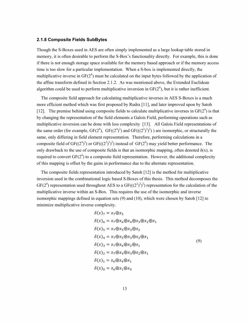
2.1.8 Composite Fields SubBytes
Though the S-Boxes used in AES are often simply implemented as a large lookup table stored in
memory, it is often desirable to perform the S-Box‟s functionality directly. For example, this is done
if there is not enough storage space available for the memory based approach or if the memory access
time is too slow for a particular implementation. When a S-box is implemented directly, the
multiplicative inverse in GF(28) must be calculated on the input bytes followed by the application of
the affine transform defined in Section 2.1.2. As was mentioned above, the Extended Euclidean
algorithm could be used to perform multiplicative inversion in GF(28), but it is rather inefficient.
The composite field approach for calculating multiplicative inverses in AES S-Boxes is a much
more efficient method which was first proposed by Rudra [11], and later improved upon by Satoh
[12]. The premise behind using composite fields to calculate multiplicative inverses in GF(28) is that
by changing the representation of the field elements a Galois Field, performing operations such as
multiplicative inversion can be done with less complexity [13]. All Galois Field representations of
the same order (for example, GF(28), GF((2
4)
2) and GF(((2
2)
2)
2) ) are isomorphic, or structurally the
same, only differing in field element representation. Therefore, performing calculations in a
composite field of GF((24)
2) or GF(((2
2)
2)
2) instead of GF(2
8) may yield better performance. The
only drawback to the use of composite fields is that an isomorphic mapping, often denoted δ(x), is
required to convert GF(28) to a composite field representation. However, the additional complexity
of this mapping is offset by the gains in performance due to the alternate representation.
The composite fields representation introduced by Satoh [12] is the method for multiplicative
inversion used in the combinational logic based S-Boxes of this thesis. This method decomposes the
GF(28) representation used throughout AES to a GF(((2
2)
2)
2) representation for the calculation of the
multiplicative inverse within an S-Box. This requires the use of the isomorphic and inverse
isomorphic mappings defined in equation sets (9) and (10), which were chosen by Satoh [12] to
minimize multiplicative inverse complexity.
(9)

14
(10)
This design builds up the composite field representation out of lower order fields. The irreducible
polynomials given in equation set (11) are used to build up to the final representation from GF(2). In
these equations, φ is the binary value of 10, while λ is the binary value 1100.
(11)
Using the equations given in (11) and the isomorphic mappings of equation sets (9) and (10), the
multiplicative inverse of any element in GF(28) can be calculated using the design pictured in Figure
8 [12][14][15]. In this design, the overall multiplicative inverse shown between δ(x) and δ-1
(x) is
performed in GF((24)
2), which in turn performs its GF(2
4) operations in GF(2
2)
2. The GF(2
2)
operations are further decomposed so that finally simple GF(2) operations are performed where
multiplication can be performed using a simple AND, and while addition remains a simple XOR.
Figure 8: Composite Fields Multiplicative Inversion
The sub operations in Figure 8 are defined as follows. The x2 operation is squaring in GF(2
4), the
Xλ is constant multiplication in GF(24), the X operation is multiplication in GF(2
4), while the x
-1 is

15
inversion in GF(24). For a more detailed description of the composite fields multiplicative inversion,
see the works of Zhang [14], and Mui [15].
2.2 Field Programmable Gate Arrays
Field Programmable Gate Arrays (FPGAs) are reprogrammable hardware platforms that are intended
as alternatives to Application Specific Integrated Circuit (ASIC) and software based processor
platforms. ASICs are custom created to perform a specific function so they are generally very fast
and efficient in terms of physical area and energy consumption and are very cheap per unit when
produced in high volumes, but have very high non-recurring engineering costs and a long time to
market. Generally they are not flexible and cannot be reprogrammed to do anything other than
perform their originally intended function. Software based processor platforms on the other hand
consist of a generic microprocessor which is programmed to perform a specific function. Generally,
they tend to be more flexible, but less efficient and have lower development times and costs.
Additionally, they are very flexible and designs can be updated or changed simply by running new
code. FPGAs fit in the grey area in between ASICs and software based processor platforms; they are
much faster and more efficient than processors, as well as more flexible and cheaper and easier to
develop for than ASICs. However, development on an FPGA is typically more expensive and time
consuming than on a processor, and the final product costs more per unit when produced in high
volumes and are slower and less efficient than they would have been had they been implemented on
an ASIC.
The speed and efficiency of FPGAs combined with their flexibility makes them very attractive for
cryptographic applications [16]. The ability to reconfigure an FPGA to use a different cryptographic
algorithm on the fly or to be able to update, modify or even replace an outdated algorithm if necessary
make them very useful for cryptosystems. Likewise, the high speeds, and subsequently throughputs,
that FPGAs are capable of running at make them very useful in high speed communications links or
servers that often require security.
Most FPGAs such as ones belonging to Altera‟s Cyclone II family [17] or Xilinx‟s Virtex II family
[18] consist of a network of configurable general purpose logic and embedded functional blocks
connected by configurable routing. General purpose logic is usually implemented as a series of
multiple input Look Up Tables (LUTs) with their outputs optionally connected to register storage
elements. Embedded functional blocks are intended to implement common operations that most
designers require with greater efficiency than is possible using general purpose logic. Commonly
available functional blocks include block RAMs, hardwired arithmetic circuits, Digital Signal
Processors (DSPs), Phase Locked Loops (PLLs) or other clock management functions, or even full
microprocessors.
16
2.2.1 Altera Cyclone II
The Altera EP2C35 Cyclone II FPGA [17] was chosen for use in this thesis. It is a relatively simple,
low cost FPGA that is widely available. The Cyclone II uses general purpose logic resources called
Logic Elements (LEs), and has 4 kb RAM, embedded multiplier and PLL embedded functional
blocks. Table 2 shows the available resources in each of the Cyclone II models. The EP2C35 was
used. Of the available device features, only the general purpose logic and block RAMs were used in
the designs presented in this thesis.
Table 2: Altera Cyclone II Resources [17]
Feature EP2C5 EP2C8 EP2C15 EP2C20 EP2C35 EP2C50 EP2C70
LEs 4,608 8,256 14,448 18,752 33,216 50,528 68,416
4 kb RAM
Blocks 26 36 52 52 105 129 250
Embedded
Multipliers 13 18 26 26 35 86 150
PLLs 2 2 4 4 4 4 4
Usable IO
Pins 158 182 315 315 475 450 622
The LEs of the Cyclone II contain a four input lookup table and an optional storage register, and
are organized into groups of 16 called Logic Array Blocks (LABs). A diagram of the layout of a LE
in normal use can be found in Figure 9 [17]. As can be seen in the diagram, the outputs from the LE
can go to multiple routing resources, and can be taken either from the register or the lookup table.
Likewise, the register can be fed by either the lookup table or another register. Note also that the
control signals used, including the clock enable, are all shared between all the LEs of a lab.
The embedded RAM blocks in the Cyclone II are each capable of storing 4 kb data and can operate
in true dual port mode. A diagram of a Cyclone II dual port memory block can be found in Figure 10.
As can be seen in the figure, each of the ports has its own set of data and address lines as well as its
own write enable and control lines. This means that both ports can be operated completely
independently of one another, can both perform any combination of reads and writes. It supports read
during write, meaning that when a write operation is performed, the written value will also appear at
the output the same as if a read had been performed with the written value already in the memory.
The memory can be operated completely synchronously with clocked inputs and outputs. This means
that it takes one clock cycle to write one value to a memory, and two to retrieve one: one to set up the
address, and a second to register the output. Each of the ports can support up to 16 bit wide outputs.

17
Therefore, if it is operated as a single port memory, output widths of up to 32 bits are possible. Block
RAMs in the Cyclone II, like in most FPGAs, are distributed evenly throughout the chip in columns.
Figure 9: Cyclone II Logic Element [17]
Figure 10: Cyclone II Block RAM [17]
The routing resources in the Cyclone II consist of local interconnects, direct links, and row and
column interconnects. A diagram of the routing network can be seen in Figure 11 [17]. Local
interconnects are the shortest routing resource and are used to connect signals between LEs that are in

18
the same LAB. Direct link interconnects are the next shortest and are used to connect signals from
adjacent LABs or functional blocks such as block RAMs. Row and column interconnects are longest
routing resources which are used to connect signals from distant blocks. It is fastest and most
efficient to use the shortest interconnect possible when connecting adjacent blocks.
Figure 11: Cyclone II Routing Resources [17]
2.3 Power and Energy Analysis
In modern digital electronics design, both power dissipation and energy consumption need to be
considered. Energy consumption can be a large concern both in mobile and backend computing
environments since it has a direct impact on battery life and electricity costs respectively. Power
dissipation is the rate at which energy is consumed and transformed mostly into heat during a
device‟s operation, and also needs to be considered to ensure that electrical components do not
overheat.
Measurements for power usage are much easier to obtain than ones for energy consumption, so
this thesis typically calculates the average amount of energy consumption based on its average power
dissipation using the fundamental equation of:
(12)
19
Where E is the energy consumed over the interval of time given by t at an average power
dissipation rate of P. Of course, for any electronic component, the amount of power dissipated is
given by the product of the voltage across the component and the current flowing through it:
(13)
2.3.1 Power Usage in FPGAs
Power usage in an FPGA, or in any digital electronic device, can be broken down into static and
dynamic components with the total amount of power dissipated as the sum of the two:
(14)
Static power is the power that is dissipated in the device due to current leakage in transistors and
occurs at all times when the device is on [19]. Since power is given by the product of voltage and
current, the static leakage power is proportional to both the supply voltage for the FPGA as well as
the leakage current. The leakage current itself is dependent on transistor junction temperature and
will increase along with the device‟s temperature.
FPGAs dissipate much more static power than ASICs, simply because there are many more
transistor based components that have leakage current flowing through them [20]. These additional
components all stem from an FPGA‟s reconfigurable nature. The configuration data for most FPGAs
is stored in SRAM based memory. When the device is powered up, every configuration bit stored in
this memory has leakage current associated with it. Similarly, the routing in FPGAs also requires
multiplexors to function properly; every multiplexor uses more logic that also has leakage current.
Finally, the use of flexible lookup tables in FPGAs for logic implementation requires more logic, and
thus has more leakage current, than the basic logic gates used in ASICs.
Dynamic power, on the other hand, is all the power that is dissipated in an FPGA due to signals
transitioning, and can be broken down into switching and short circuit power [19], Switching power
is the power dissipated through the changing and discharging of capacitances associated with
transistors or routing, while short circuit power is the power dissipated by current flowing from
voltage supply to ground between the pair of CMOS logic transistors while both transistors are
momentarily on during a logic transition. The equation for dynamic power is:
(15)
The left term of the equation defines switching power, while the right defines short circuit power.
Both parts of dynamic power are affected by the frequency that the device is operating at, f, as well as
the activity factor of the component. The activity factor, or switching rate, is the percentage of clock
cycles where the signal transitions. If a component goes unused or its output doesn‟t change for a
number of clock cycles its activity factor will be below 100%. Glitching or unnecessary signal
20
transitions on the other hand, can cause the activity factor to be greater than 100%, increasing
dynamic power consumption. The switching power is also dependent on the capacitance, C, of the
component or routing, as well as the supply voltage, while the short circuit power is dependent on the
amount of current flowing between the transistors as well the supply voltage and the amount of time
both transistors are on.
FPGAs also dissipate more static power than ASICs. The most obvious reason for this is that the
longer routing lengths and more complex routing that is required for FPGAs results in larger
capacitance on the routing wires and thus more switching dynamic power. Additionally however, the
programmable switches located on the routing paths increase capacitance even further, resulting in
even more power dissipation [20].
Though there is often very little that an FPGA designer can do to mitigate static power
consumption for a given FPGA platform, dynamic power consumption can vary greatly depending on
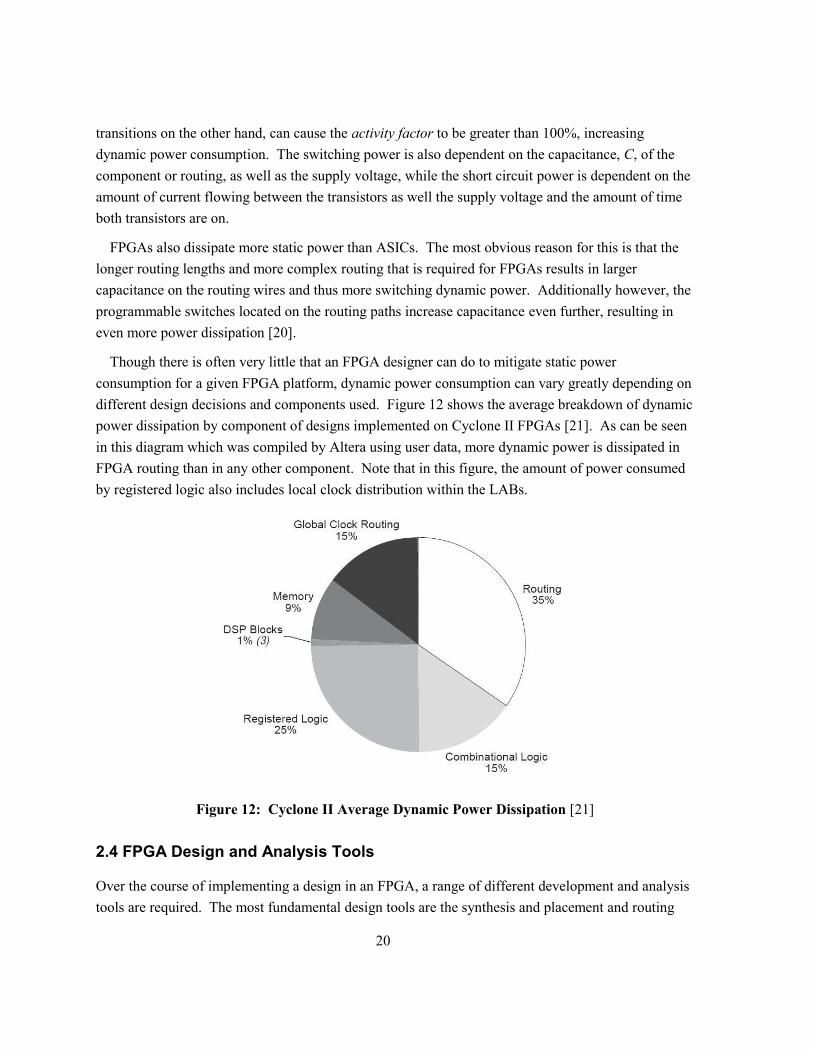
different design decisions and components used. Figure 12 shows the average breakdown of dynamic
power dissipation by component of designs implemented on Cyclone II FPGAs [21]. As can be seen
in this diagram which was compiled by Altera using user data, more dynamic power is dissipated in
FPGA routing than in any other component. Note that in this figure, the amount of power consumed
by registered logic also includes local clock distribution within the LABs.
Figure 12: Cyclone II Average Dynamic Power Dissipation [21]
2.4 FPGA Design and Analysis Tools
Over the course of implementing a design in an FPGA, a range of different development and analysis
tools are required. The most fundamental design tools are the synthesis and placement and routing
21
tools that are required to compile a FPGA design, while simulation and power analysis tools are very
useful in order to verify that a design meets its specifications.
Synthesis tools are used to interpret the source Hardware Description Language (HDL) code
(usually VHDL or Verilog) and transform it into its intended logic functions. The tools typically
convert the HDL code to a Register Transfer Level (RTL) netlist which defines the logical functions
that must be performed and how they fit between the synchronous register elements of a design.
These logical functions can then be optimized and mapped to the resources that are available in the
target FPGA. Synthesis tools are commonly provided by FPGA manufacturers such as Altera or
Xilinx or by third party Electronic Design Automation (EDA) tool developers like Mentor Graphics
or Synplicity.
Placement and routing tools, on the other hand, are used to select where the resources required to
implement the design are placed in the target FPGA and how they should be connected together.
They are usually provided directly from the FPGA manufacturer.
Simulation tools are used to test the functionality of designs both before they have been placed and
routed for a specific FPGA and after. Before a design has been fitted for a specific device, simulation
is used to ensure that the VHDL or Verilog code is functionally correct. After placement and routing,
timing information for the specific components used in the design are available, and the design can be
tested to make sure it will work on the specific FPGA. The most popular simulation tool is Mentor
Graphic‟s ModelSim, though FPGA manufacturers typically provide their own simulation tools as
well.
Power analysis tools can be used to estimate how much power a design will use on a specific
device before being actually uploaded to it [19]. The tools have a model of the power consumption of
each of the device‟s components and can evaluate how much power a design will dissipate based on
the usage of each of the components by a design. The tools determine which routing, logical and
functional resources are used by a design using information from the post place and route design file,
and use frequency and activity factor information obtained either by estimation or from post place and
route simulation of the design. Due to the detailed device information that is required to create an
accurate power analysis tool, such tools are provided by the FPGA manufacturers. Xilinx provides
the Xpower power analyzer [22] while Altera offers the PowerPlay Power Analyzer [4].
Early estimator power analysis spreadsheets and web sites are also available from Xilinx and Altera
[23] [24] to estimate power consumption, but they are often less reliable than the full fledged tools
described above. Since they cannot have access to simulation data when assessing power usage, they
must rely only on the amount of resource utilization and estimated switching activity.

22
2.4.1 Altera Quartus II Design and Analysis Tools
Altera FPGAs were chosen for study in this thesis in order to gain the advantages of using the power
analysis and power driven synthesis and placement and routing features of Altera‟s Quartus II FPGA
design software. This thesis uses the Quartus II integrated synthesizer, fitter, and simulator as well as
the Quartus II PowerPlay Power Analyzer.
The PowerPlay Power analyzer is a robust software tool which provides estimates of power
consumption in Altera FPGAs to within 10% of the true power consumption as measured on a
physical device [19]. As was stated above, the software bases its analysis on the resources used, and
can estimate the signal activities in the design or use post place and route simulation results to
determine the actual signal activities while the device is performing its intended function. The
simulation data method is much more accurate provided that the simulation exercises the entire
design using a variety of different typical inputs [4]. When this method is used, the power usage
estimates will be the power that is used by the device while performing the operations used in the
simulation. The PowerPlay Power analyzer is capable of accepting simulation data in the form of
Value Change Dumps (VCDs) or Signal Activity Files (SAFs). Value change dump files can be
output by the Quartus II integrated simulator, or by third party simulators such as ModelSim. Signal
activity files can only be output by the Quartus II integrated simulator, but they are much smaller in
size and easier to manage than their equivalent VCD files. The power analyzer also has an option
called glitch filtering. The glitch filtering option is used to cause the power analyzer to disregard
glitches that occur in rapid succession in simulation and would not propagate in a physical device.
The Quartus II integrated simulator is a simple simulator that is a part of the Quartus II
development software package [25]. It does however, have two notable features: the ability to output
SAF files from simulation, and the ability to take simple text based files as test bench inputs. The
use of SAF files in power analysis is preferable to the use of VCD files due to their small size. The
simulator is also able to use text based table test bench files which can be easily generated
automatically by other programs.
The Quartus II integrated synthesizer allows for power driven synthesis that can result in designs
that dissipate less power [26] [21]. When the extra power effort synthesis option is used, the
synthesizer attempts to synthesize logic and memory such that the minimum amount of power is used.
Power aware logic mapping is performed in which logic is rearranged if possible in an attempt to
eliminate routing segments that are likely to have high activity factors. Power aware memory
mapping attempts to structure memories such that as few memories as possible are enabled at once.
Often memories are required by designs that are larger than the blocks available in an FPGA. In such
cases there may be multiple ways the memory could be divided into the block sizes available; power
aware memory mapping chooses the structure that is most likely to yield the lowest power
dissipation. An example is pictured in Figure 13 [21]. If a memory that was capable of storing 4 k 4

23
bit values was required by a design that is to be implemented on an FPGA with only 4 kb memory
blocks, the most obvious way of implementing it would be to use four 4 kb blocks in parallel that
each output a single bit. This is pictured in the right hand side of Figure 13. However, if power
aware memory mapping is used power savings could be obtained by implementing the four memories
as storing 1k 4 bit values each with only one memory being enabled at any given time. This is shown
in the left hand side of Figure 13. This power optimization comes at the cost of an additional decoder
that would be required to convert the upper most address bits to clock enable lines for the four
memories and an additional multiplexor on the output.
The Quartus II fitter allows for power driven placement and routing as well as adjustable placement
and routing effort [26] [21]. When the extra power effort fitter option is used, the fitter can use a
previously generated SAF file for the design to try to minimize the distance that wires with high
activity factors have to travel. Recall that the largest component of an FPGAs dynamic power
consumption occurs in its routing resources. If components that are connected by wires that have a
high activity factor can be placed closer together such that shorter lower capacitance local
interconnects or direct links can be used, less power will be dissipated in the wire. This technique can
result in large power savings, but also requires that a SAF file from a previously compiled version of
the same design be available. This leads to a more complicated design flow in which the design must
be compiled then simulated to generate an initial SAF file, then placed and routed again with the new
signal activity information. By default, the fitter will use the bare minimum amount of computational
effort to place and route a design while still meeting any timing goals that are specified. The standard
fitter effort option changes this so that the maximum amount of computational effort is used
regardless of the specified timing goals.
Figure 13: Power Aware Memory Synthesis [21]
24
2.5 Chapter Summary
This chapter introduced important background information required for the understanding of the rest
of this thesis. Specifically, the Advanced Encryption Standard and Field Programmable Gate Arrays
along with the basics of their power analysis were introduced. The Altera Cyclone II and Quartus II
design tools used in this thesis were also presented. The next chapter reviews some of the previous
research that has been performed in the areas of low power FPGA design methodologies and FPGA
based AES implementations.

25
Chapter 3
Related Work
The purpose of this chapter is to introduce some of the previous work that has been done in the areas
of low power FPGA design techniques as well as AES FPGA implementations. Section 3.1
introduces low power FPGA design methodologies while Sections 3.2, 3.3 and 3.4 discuss previous
high throughput, low area, and low power FPGA based AES implementations.
3.1 Low Power FPGA Design Methodologies
Low power design techniques are often more difficult to utilize in FPGAs than they are in ASICs.
This section discusses pipelining, use of embedded functional blocks, clock gating, voltage scaling,
and use of extra flip flops with phase shifted clock strategies that have been proposed to lower the
power dissipation in FPGAs.
Pipelining is a basic digital design strategy that is frequently used to increase the operating
frequency and throughput of designs, but it can also have a large impact on the dynamic power
consumption of FPGA designs [21] [27]. Glitching though multiple layers of combinational logic
and routing resources accounts for a large amount of power consumption in FPGAs. By inserting
pipelining registers to break up these large runs of combinational logic and routing, glitches are
unable to propagate as far, and power savings are obtained. Studies by Altera show that by applying
basic pipeline techniques, dynamic power reductions of up to 31% are possible using a Cyclone II
[21]. An academic study by Wilton shows that heavy pipelining can reduce power consumption by
between 40% and 82% depending on the specific FPGA and the design being pipelined. [27]
The use of the embedded function blocks in FPGAs instead of general purpose logic elements can
also reduce dynamic power consumption [21] [28]. Embedded functions and RAM blocks in FPGAs
basically function as ASIC circuits within the FPGA fabric; they do not have any programmable
routing within them. Therefore their internal routing is much more power efficient than the routing
used for general purpose logic. If some functionality required of the FPGA can be implemented by
an embedded functional block, it will generally be more efficient than if it were implemented in
general purpose logic. Kuon performed a generalized study that shows that the dynamic power
consumption in an FPGA can be reduced almost by half though the use of embedded functional
blocks [28], while an Altera study showed that the use of embedded multipliers could reduce dynamic
power consumption by up to 88% in a Cyclone II [21]. This same study showed that the use of block
RAMs in a Cyclone II could reduce dynamic power consumption by up to 23%.
Clock gating is a commonly used ASIC dynamic power reduction technique that can also be
applied to FPGAs albeit less effectively and in an indirect way [21] [29]. Clock gating involves
blocking off or gating a clock when the operation of the components it is driving is not required. This

26
is accomplished by ANDing the clock with a control signal. Blocking off the clock not only prevents
clock switching in unneeded portions of the design, but also prevents unnecessary toggling of data
signals there as well. Unfortunately, FPGA clock networks use special low skew routing resources
that do not contain user configurable logic so direct clock gating as is done in ASICs is not
recommended [21]. FPGAs however, can use a form of gating where the clock is still run to all
registers in the general purpose logic network of an FPGA, but their outputs are fed back to their
inputs using a register feedback path like the one seen in Figure 9 when the component‟s functionality
is not required. An academic study by Zhang showed that this form of gating, which essentially
prevents outputs on registers from toggling, was able to reduce the dynamic power consumption in
FPGAs by 45% to 87% depending on the design when the gate was applied 100% of the time [29].
The same study showed that traditional clock gating in ASICs was able to reduce the dynamic power
consumption by 82% to 99% under the same conditions. Additionally, most FPGA resources include
a clock enable signal which disables the clock for the entire embedded functional block or general
purpose logic block (LAB in the Cyclone II), and FPGAs typically shut down the clock for sections
of the chip that are not configured for the current design [21].
Dynamic voltage scaling is another technique that can be used to reduce both static and dynamic
power consumption in FPGAs [30]. Reducing the supply voltage to an FPGA will reduce both the
static and dynamic power dissipation in a design, but will also reduce the maximum operating
frequency and could cause the device to function improperly if it is reduced too far. Dynamic voltage
scaling seeks to reduce the supply voltage and power consumption of a design until it can barely meet
its timing requirements and still function properly. This is complicated by the fact that the amount of
delay in the circuit is also dependant on the device‟s temperature which can change during operation.
Thus, dynamic voltage scaling also requires additional FPGA overhead in the form of some logic
usage for delay monitoring as well as hardware overhead external to the FPGA used for supply
voltage adjustments. The FPGA itself does not require modification however, and total core power
savings between 4% and 54% for a variety of designs have been observed.
The use of extra flip flops driven by a phase shifted clock is another FPGA power reduction
technique which has been proposed [31]. This strategy is similar to pipelining in that it reduces
dynamic power consumption by using registers to prevent glitches from propagating through the
design. The difference in this case is that the registers added are driven by an out of phase clock to
get the benefits of glitch blockage without increasing the latency of the design as pipelining would.
This allows existing designs to be more easily modified for dynamic power savings than pipelining
would allow, but also doesn‟t come with the added benefits of increased maximum operating
frequency and throughput that pipelining provides. In fact, insertion of additional pipelines actually
slightly reduces the maximum frequency that the design is capable of attaining. This technique
showed dynamic power reduction of between 5% and 70% depending on the design assessed, which
is comparable to the savings obtained through the use of pipelining.

27
3.2 High Throughput FPGA Based AES Implementations
There have been many FPGA based AES designs which focused on obtaining high throughputs.
These designs often fully unroll the iterative round structure of AES and rely heavily on pipelining
within each round to increase throughput. Unrolling the AES round structure is the practice of
implementing separate hardware for each of AES‟s rounds instead of feeding data values through the
same round hardware repeatedly. This allows new data values to be accepted every clock cycle as
previous data values are passed onto new round hardware. Adding pipeline stages within each round
increases latency, but allows for higher clock frequencies and thus higher throughputs. Such designs
typically avoid the use of block RAMs because they insert large unbreakable delays in the data path
and implement S-boxes using a more pipeline friendly composite fields approach. They also tend to
expand keys on the fly along with cipher operations and discard them when they are no longer
required in order to avoid having to store large amounts of key data for the multiple encryption and
decryption operations which will be occurring along its lengthy pipeline at any given time. High
throughput FPGA AES designs typically achieve throughputs above 20 Gbps and are intended for use
in cryptographic co-processors that need to simultaneously handle multiple security sessions running
in a backend server environment. Examples of very good high throughput FPGA AES include
implementations by Zhang [13], Iyer [32] and Good [33] [34].
3.3 Low Area FPGA Based AES Implementations
There are also many FPGA based AES implementations that are focused on using very little area and
being able to fit on as small an FPGA as possible. Many of these designs also claim to be useful for
low power applications, but rarely include an accompanying power analysis. Most designs rely
heavily on the use of embedded functional blocks and data path width reduction strategies to achieve
low area usage. Embedded functional blocks make better use of chip area than general purpose logic
since they do not require additional programmable routing resources. Reducing the data path width
of an AES implementation means that multiple runs through the same hardware are required to
perform a single round of operation. A well known example of this is a design by Codowiec and Gaj
[35] which uses a 32 bit wide data path. Only four S-Boxes and one MixColumns modules are used
with a single round of data processing requiring the use of them four times. Other examples of
excellent low area FPGA AES include implementations by Rouvroy [36], Good [37] and Huang [38].
3.4 Low Power FPGA Based AES Implementations
Most likely due to the relatively high power consumption in FPGAs when compared to ASICs, there
has been very little work performed in the area of low power or energy efficient AES
implementations on FPGAs. Three designs that did make attempts to achieve low power operation
and included power usage estimates are discussed.

28
Alam et al implemented a T-Box based FPGA AES design intended to have high throughput and
low power usage[39]. The T-Box method combines the SubBytes, ShiftRows, and MixColumns of a
round into four table lookups per column with each column of table lookups requiring 4 kB of
memory storage to implement [8]. For comparison purposes, this is four times the memory per
column than would be required to implement the S-boxes alone. This method was originally intended
for software applications since it can be very efficiently implemented in systems with a 32 bit data
path and large amounts of available memory. It also has the potential to be very power and energy
efficient in an FPGA since it relies more on the embedded RAM blocks than general purpose logic.
The design implemented is capable of performing encryption and key expansion, but not decryption
in order to conserve memory resources. In a further attempt to conserve memory resources, the
design also uses a 32 bit data path requiring four clock cycles per round. Additionally a 128 bit data
path one clock cycle per round version is discussed, but not fully implemented. The key expansion in
the design must be performed before encryption can begin, and the expanded key is stored and used
on all plaintexts until a key change takes place. The design fully unrolls the iterative AES loop, so
plaintexts can be continually passed through it. The authors were able to estimate core dynamic
power dissipation of 154 mW on a Xilinx Vertex II running at 10 MHz by using Xilinx‟s XPower
tool. The estimate was based on signal activity data obtained by performing timing simulation on the
design‟s first round.
Rejeb et al implemented several low data path width FPGA designs which were intended to
achieve low power and low area. The designs used several techniques designed to lower their power
dissipation. The first method was the use of a novel GF((24)
2) composite fields S-Box intended to be
compact and power efficient. The second method is use of low data path width components to reduce
the amount of hardware in use concurrently. The three implemented designs use one, two and four S-
Box components in parallel. Finally, the structure is set up so that components are disabled when
there is not enough data available for them to work on. The designs are capable of performing key
expansion, encryption and decryption, though no details are given about the key expander‟s
functionality. Designs using one, two and four parallel S-Boxes performing at 18.56, 45.5 and 68
Mbps were estimated to dissipate 137, 158 and 169 mW of dynamic power on a Xilinx Virtex FPGA.
Power estimates were obtained using the Xilinx Power Estimator Spreadsheet based on synthesis
report data.
Katashita et al proposed the FPGA power reduction technique of using extra flip flops driven by a
phase shifted clock, and was successful in applying it to AES for power savings [31]. The technique
was applied to two AES designs which used two different methods to implement the AES S-Boxes;
the first method used asynchronous block RAMs for S-Boxes, while the second manually
implemented them using composite fields performing multiplicative inversion in GF((24)
2). Both of
the designs used an iterative round structure with a 128 bit data path which implements the hardware
for a single round then cycles the data through it 11 times. Since the use of extra phase shifted flip

29
flops is intended as a replacement to pipelining, there are no pipeline registers within the round
structures of the designs, and both designs are able to perform an entire round in a single clock cycle.
The designs were capable of performing both encryption and decryption, but not key expansion, and
used a static pre expanded key stored in block memory. Using the proposed power reduction
technique, the block RAM based design was able to achieve dynamic power consumptions of 309.255
mW and 332.460 mW for encryption and decryption respectively when run at 66.66 MHz, while the
composite fields based design was able to achieve 306.690 mW and 319.170 mW when run at 50
MHz. All of the power analysis was performed using Xilinx‟s XPower tool based on signal activity
data obtained from timing simulation for a Virtex II.
3.5 Chapter Summary
This chapter summarized some of the important research that has been performed in the areas of
FPGA based AES implementations and FPGA power reduction design techniques. Though there has
been a great deal of research focusing on the development of high throughput and low area utilization
FPGA based AES designs, there has been very little research focusing on lower power or higher
energy efficiency. This is likely due to the higher power consumption which is typically observed in
FPGAs combined with the awkwardness and limited availability of power reducing design techniques
for the platform. Further frustrating the development of lower power or energy efficient AES
implementations for FPGAs is the difficulty in estimating the power consumption of a given design.
Most research simply does not include power consumption data for proposed designs, likely due to
the cumbersome simulation process required to gain accurate estimates. Of the three discussed
designs that did include power consumption estimates, only the designs by Katashita et al [31]
obtained power estimations using full simulation data; the other two relied on estimates from partial
simulation or synthesis data only.
The following three chapters present the research done in this thesis to overcome some of the issues
surrounding the implementation of energy efficient FPGA based AES. Chapter 4 discusses low
power and energy efficiency strategies used within the context of AES and presents a new FPGA
dynamic power reduction technique called Opportunistic Combinational Operand Gating. Chapter 5
presents the proposed energy efficient AES design along with several AES cipher designs used to
evaluate the effectiveness of the chosen power reduction strategies, while Chapter 6 introduces the
methodology employed to assess energy efficiency using the developed AES Energy Analyzer script.

30
Chapter 4
Design Methodology
This chapter describes the methodology and strategies used to develop a high energy efficiency
Advanced Encryption Standard design. Section 4.1 starts off the chapter by discussing the overall
design goal as well as the rationale behind choosing to target energy efficiency. Section 4.2 discusses
the energy efficiency strategies and techniques that were employed while Section 4.3 details the
process used to evaluate the effectiveness of the chosen strategies and use them to create an energy
efficient full AES design.
4.1 Design Goals
One of the main goals of this thesis is to develop a full featured FPGA AES implementation which is
as energy efficient as possible. A full AES implementation includes key expansion functionality as
well as both encryption and decryption functions. To be as flexible as possible, this design must also
have the ability to perform encryption in parallel with key expansion. That is, it is important that the
design not have to fully expand a key before encryption takes place.
High energy efficiency was chosen as the target for the design as opposed to low power
consumption as is often done in ASIC design. Low power consumption is an important goal for
many applications in which AES is used such as RFIDs and sensor networks [5], but it is simply an
impractical goal for FPGA based designs. As was discussed in Section 2.3.1, the larger amount of
static and dynamic power consumption in most FPGAs make them a poor choice for low power
applications when compared to ASICs regardless of dynamic power reduction techniques which
could be used. Though FPGA based designs simply cannot achieve low power consumption, they can
achieve a respectable level of energy efficiency by offsetting their large power dissipation with a
high throughput; FPGAs are very useful for System on Chip, special purpose co-processing and other
potentially high throughput embedded systems applications where lower energy consumption would
still be advantageous. Such applications are also likely to require security features that require AES.
Given FPGAs inability to achieve low power and their likelihood of being used in high throughput
designs, high energy efficiency is a much better design goal for FPGA based AES implementations
than simple low power consumption.
4.2 Energy Efficiency Design Strategies
There were several different strategies used to achieve energy efficiency in AES. The high level
strategy of adding flexibility to the key schedule was intended to make the design more energy
efficient at the algorithm level, while lower level design techniques such as register clock enable and
combinational operand gating were used to reduce the amount of unnecessary logic switching, and
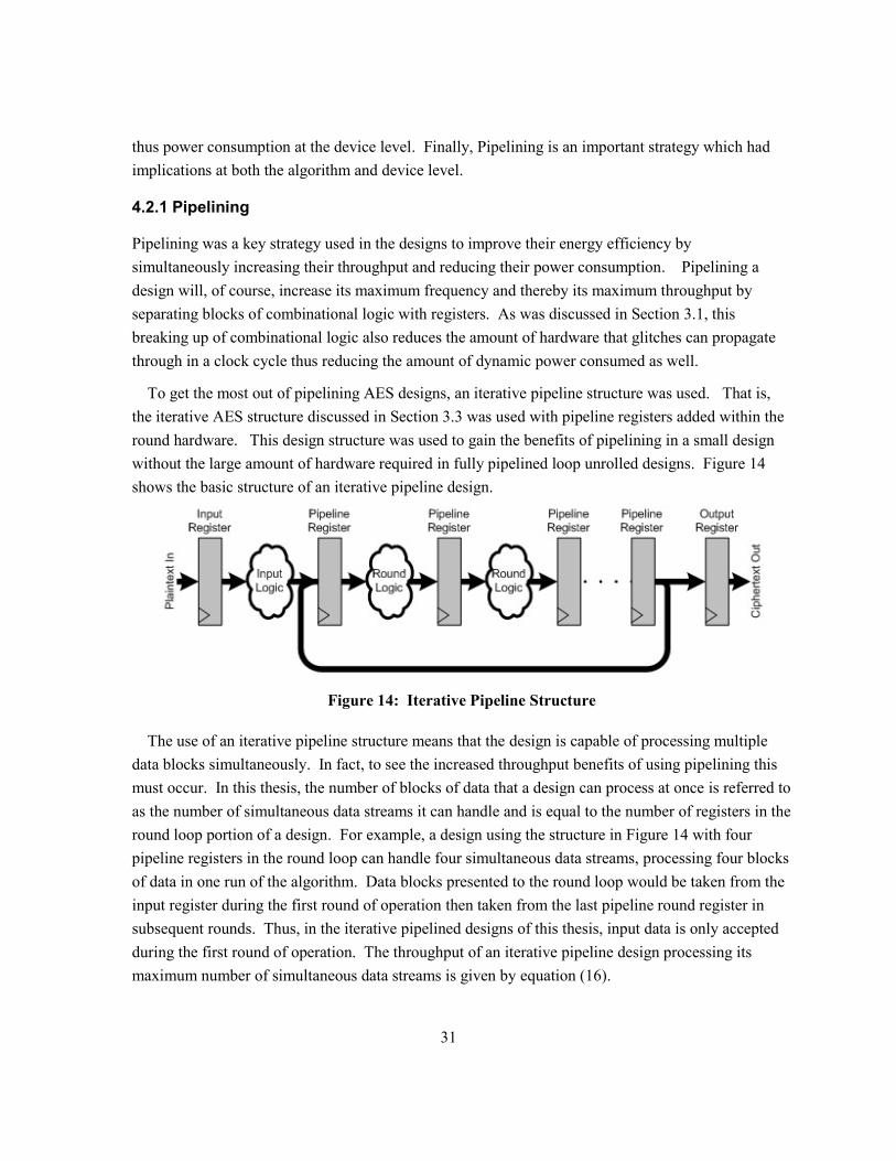
31
thus power consumption at the device level. Finally, Pipelining is an important strategy which had
implications at both the algorithm and device level.
4.2.1 Pipelining
Pipelining was a key strategy used in the designs to improve their energy efficiency by
simultaneously increasing their throughput and reducing their power consumption. Pipelining a
design will, of course, increase its maximum frequency and thereby its maximum throughput by
separating blocks of combinational logic with registers. As was discussed in Section 3.1, this
breaking up of combinational logic also reduces the amount of hardware that glitches can propagate
through in a clock cycle thus reducing the amount of dynamic power consumed as well.
To get the most out of pipelining AES designs, an iterative pipeline structure was used. That is,
the iterative AES structure discussed in Section 3.3 was used with pipeline registers added within the
round hardware. This design structure was used to gain the benefits of pipelining in a small design
without the large amount of hardware required in fully pipelined loop unrolled designs. Figure 14
shows the basic structure of an iterative pipeline design.
Figure 14: Iterative Pipeline Structure
The use of an iterative pipeline structure means that the design is capable of processing multiple
data blocks simultaneously. In fact, to see the increased throughput benefits of using pipelining this
must occur. In this thesis, the number of blocks of data that a design can process at once is referred to
as the number of simultaneous data streams it can handle and is equal to the number of registers in the
round loop portion of a design. For example, a design using the structure in Figure 14 with four
pipeline registers in the round loop can handle four simultaneous data streams, processing four blocks
of data in one run of the algorithm. Data blocks presented to the round loop would be taken from the
input register during the first round of operation then taken from the last pipeline round register in
subsequent rounds. Thus, in the iterative pipelined designs of this thesis, input data is only accepted
during the first round of operation. The throughput of an iterative pipeline design processing its
maximum number of simultaneous data streams is given by equation (16).
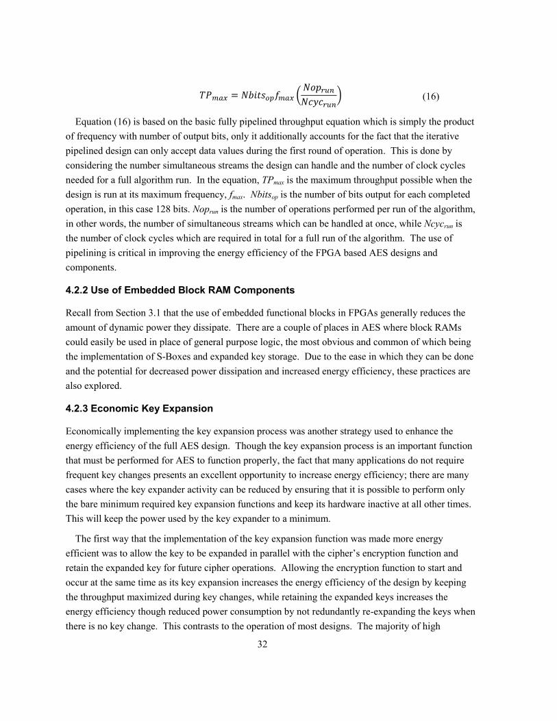
32
(16)
Equation (16) is based on the basic fully pipelined throughput equation which is simply the product
of frequency with number of output bits, only it additionally accounts for the fact that the iterative
pipelined design can only accept data values during the first round of operation. This is done by
considering the number simultaneous streams the design can handle and the number of clock cycles
needed for a full algorithm run. In the equation, TPmax is the maximum throughput possible when the
design is run at its maximum frequency, fmax. Nbitsop is the number of bits output for each completed
operation, in this case 128 bits. Noprun is the number of operations performed per run of the algorithm,
in other words, the number of simultaneous streams which can be handled at once, while Ncycrun is
the number of clock cycles which are required in total for a full run of the algorithm. The use of
pipelining is critical in improving the energy efficiency of the FPGA based AES designs and
components.
4.2.2 Use of Embedded Block RAM Components
Recall from Section 3.1 that the use of embedded functional blocks in FPGAs generally reduces the
amount of dynamic power they dissipate. There are a couple of places in AES where block RAMs
could easily be used in place of general purpose logic, the most obvious and common of which being
the implementation of S-Boxes and expanded key storage. Due to the ease in which they can be done
and the potential for decreased power dissipation and increased energy efficiency, these practices are
also explored.
4.2.3 Economic Key Expansion
Economically implementing the key expansion process was another strategy used to enhance the
energy efficiency of the full AES design. Though the key expansion process is an important function
that must be performed for AES to function properly, the fact that many applications do not require
frequent key changes presents an excellent opportunity to increase energy efficiency; there are many
cases where the key expander activity can be reduced by ensuring that it is possible to perform only
the bare minimum required key expansion functions and keep its hardware inactive at all other times.
This will keep the power used by the key expander to a minimum.
The first way that the implementation of the key expansion function was made more energy
efficient was to allow the key to be expanded in parallel with the cipher‟s encryption function and
retain the expanded key for future cipher operations. Allowing the encryption function to start and
occur at the same time as its key expansion increases the energy efficiency of the design by keeping
the throughput maximized during key changes, while retaining the expanded keys increases the
energy efficiency though reduced power consumption by not redundantly re-expanding the keys when
there is no key change. This contrasts to the operation of most designs. The majority of high

33
throughput designs simply expand the key on the fly for every operation while the majority of low
power designs expand the key separately before cipher operation at the expense of throughput.
Another way that the efficiency of the key expander is increased is by not requiring that keys be
expanded for unused data streams. As was noted in Section 4.2.1, iteratively pipelining the AES
design means that it is possible to operate on multiple independent streams of data, and each of these
must be capable of using its own key which can be expanded when required independently of the
others. When not operating at peak capacity, it is possible that the use of all of the available data
streams simultaneously would not be required; in such cases, it would be wasteful to expand keys for
the unused data streams.
Finally, the efficiency of the key expander can also be increased by not requiring that reverse key
expansion be performed for a stream unless the decryption function will be used for that stream. In
many applications, one of the parties will need to perform only encryption or decryption but not both
in a session, and there are many modes of operation that do not require the use of the decryption
function at all. Recall from Section 2.1.7, that the equivalent inverse cipher structure requires
additional processing on the expanded key to obtain the reverse expanded key. This additional
processing would be a waste of power if the cipher only needed to perform the encryption function.
4.2.4 Register Clock Enable Gating
The use of the clock enable signals on registers of the AES designs was another strategy used to
increase their energy efficiency by reducing the amount of dynamic power consumption. Recall from
Section 3.1 that register clock enable gating is a commonly used power reduction technique which is
used in FPGA based designs. The register clock enable signal is used to prevent the register from
latching new input values, and can even be used to prevent the clock from being propagated to all of
the registers in a LAB since they all share a common clock enable signal.
The main use of register clock enable gating is to prevent invalid data from propagating though the
energy efficient full AES design where they would cause unnecessary signal transitions and power
consumption. Each parcel of valid data is accompanied by a valid bit which is used as the clock
enable signal for the next register in the data path. Using this technique, the AES hardware is only
active for valid streams of data. The use of this scheme is also able to prevent activity in the key
expander when no key change is required. Additionally, this also prevents activity as a whole when
the design is idle with no data being presented. As an example of this technique, Figure 15 shows the
propagation of a single data value though the iterative pipeline cipher structure introduced earlier.

34
Figure 15: Single Valid Data Propagation in Iterative Pipeline Structure
Figure 15 shows how the use of the valid bit technique prevents unnecessary signal transitions in
the iterative pipeline cipher. In each of the diagrams the darkened lines are paths in which data is
propagating and transitions may occur while the lighter paths are ones that are disabled due to the
clock enable signal where transitions cannot occur. Figure 15a shows the design when a valid data
parcel is placed at its input register and the in valid signal is high. All other data paths are disabled
since there are no valid data parcels in the design. Figure 15b shows the design one clock cycle after
the valid data parcel has been read in. At this point, the only area where signals can be transitioning

35
is in the input logic section before the round loop. Figure 15c shows the design two clock cycles after
the data parcel was supplied. By this time, the input logic has been disabled again, and the only logic
where signal transitions would be taking place would be in the first stage of the round loop. This
process of one stage of logic being enabled at a time would continue from here until the data parcel
has gone though all of the AES rounds and been output. Though this example showed only one valid
data parcel propagating though the design, it of course is possible to have multiple valid data parcels
processed sequentially at the same time.
4.2.5 Opportunistic Combinational Operand Gating
The use of operand gating using excess combinational logic resources was also done to increase
energy efficiency by reducing the amount of dynamic power consumption. Operand gating is a
commonly used processor power reduction technique in which unused portions of the data path are
gated off to conserve energy [40]. This technique could be used quite effectively in FPGAs and in
could even be done with no additional combinational logic usage in some situations. Recall from
Section 2.2 that combinational logic in most FPGAs is implemented in lookup tables that have a fixed
number of inputs. For example, devices in the Altera Cyclone II family all use four input LUTs.
Depending on the specific design, it is not uncommon for some lookup table inputs to go unused. In
these cases, operand gating could be obtained in the function being implemented at no additional
hardware cost simply by utilizing the previously unused LUT input as a gating signal. An example of
this technique, referred to as Opportunistic Combinational Operand Gating (OCOG) and developed as
part of the contributions of this thesis, can be seen in Figure 16.
Two lookup tables implementing the same three input function with and without gating are shown
in Figure 16. The design in this example requires a three input function while the device being used
utilizes four input LUTs. This means that there will be one unused input on the LUT implementing
this function when the design is mapped to the target FPGA as can be seen in Figure 16a. If gating
would be useful for this function to reduce the power consumption of the design, it can be
implemented at no additional hardware cost by utilizing this unused input as can be seen in Figure
16b.
It should be noted however, that the use of this technique might not always be advantageous. Of
course, if the function that is required fits exactly into one or more LUTs on its own with no unused
inputs, adding a gating signal will require an additional LUT, nullifying the power savings obtained
by gating. Additionally, even if it is possible to implement without additional LUT usage,
implementing gating always adds an additional gating signal, increasing routing congestion and
potentially decreasing the effect on power reduction.

36
Figure 16: Opportunistic Combinational Operand Gating Example
Implementing combinational gating in practice can be quite complex, and care must be taken to
ensure that no extra hardware is accidentally added to the design in the process. Look Up Tables with
gating signals added often must be manually instantiated to ensure that they are not optimized away
by the FPGA design tools. Though this does ensure that the gating signals are included, preventing
the tools from being able to optimize areas of design also means that it may end up being larger or
more complex than is necessary, often undoing any energy efficiency gains. In order to get the
benefits of allowing optimization to be performed while still using operand gating, a two step
approach is taken. First, the design is implemented without any operand gating to allow the design
tools to perform as many optimizations as possible. The resulting logic structure is then examined
post technology mapping to determine what the optimal logic structure is as well as to find places
where combinational operand gating could be performed. The design can then be re-implemented
using an HDL coding structure that follows the optimized logic structure with the identified LUTs
manually instantiated to perform combinational gating. This strategy ensures that an optimized logic
structure is used and combinational operand gating can be performed opportunistically with no
additional hardware resources used.
37
The main use of combinational operand gating in the AES designs was to gate out specialized
encryption or decryption hardware when the converse operation was in use. This technique was
experimented with in both the S-Box and MixColumns designs, and its use in these components is
discussed further in Sections 5.2 and 5.3.
4.3 Methodology to Develop a High Energy Efficiency Full AES Design
To effectively use the strategies discussed in this chapter to develop a highly energy efficient full
AES design it is important to be able to tell how effective each strategy was, both in reducing power
dissipation and increasing energy efficiency. To determine this, each strategy was used separately in
its own cipher design and evaluated on the basis of power dissipation and energy efficiency. A
comparison of the effectiveness of the strategies was made by observing their effects on the
implemented ciphers.
Using a combination of the most effective strategies, an energy efficient cipher can be developed
and used as the basis of an energy efficient full AES design which includes key expansion
functionality. The main focus of this design methodology was to develop a highly energy efficient
cipher, even, if necessary, it was at the expense of a less efficient key expander. Allowing for parallel
encryption and key expansion operation as was discussed in 4.2.3 means that cipher and key
expansion hardware must take an equal number of clock cycles per round for processing, and the key
expander must have each round key ready in time for it to be added in the cipher‟s operation. Since
this constraint makes it impossible to design both the cipher and key expander completely
independently of each, the decision was made to develop a highly efficient cipher then design the key
expander to be as efficient as possible while meeting the cipher‟s requirements. The main reason for
this is simply that the cipher is used far more often than the key expander in actual applications.
Encryption or decryption is almost always performed on multiple blocks of data using the same key
resulting in much greater cipher than key expansion usage. Even in the worst case situation in which
each block of data is operated on with a different key, the key expander is only used as often as the
cipher and never more. Given how much more often the cipher hardware is likely to be used than the
key expander hardware it makes more sense to prioritize its energy efficiency.
4.4 Chapter Summary
This chapter presented the methodology used to develop an energy efficient FPGA implementation of
AES. Most notably, the strategies used to increase the efficiency of AES were discussed and a new
dynamic power reduction technique called Opportunistic Combinational Operand Gating was
presented. The following chapter details the cipher designs used to evaluate these energy efficiency
strategies within the context of AES and gives the implementation details of the proposed full energy
efficient AES design.
38
Chapter 5
Advanced Encryption Standard Designs
The purpose of this chapter is to introduce and discuss the AES implementations which were
designed based on the strategies presented in Chapter 4. The chapter starts with Section 5.1
introducing the overall structure used in the test cipher and full AES implementations. The S-Box and
MixColumns architectures used to assess the effects of the various energy efficiency strategies are
presented in Sections 5.2 and 5.3. Section 5.4 details ciphers which were implemented and tested to
investigate the effectiveness of these strategies. Finally, Section 5.5 presents the proposed energy
efficient full AES design which includes a key expander.
The strategies of pipelining, OCOG and block RAM usage are illustrated in their own ciphers, with
the use of register clock enable gating performed in the cipher which combines the most effective
techniques. Of course, the economic key expansion strategies cannot be applied until the key
expander functionality is added in the Full AES design.
5.1 Balanced AES Round Structure
The implementations in this thesis do not use the standard AES round structure defined in Section
2.1.1. To allow for easier hardware reuse between the encryption and decryption functions, the
equivalent inverse cipher discussed in Section 2.1.7 is used instead. Additionally, a balanced round
structure was used which has 10 rounds of equal length. This contrasts with the standard structure
which consists of an initial key addition followed by 9 identical middle rounds and a final short
round. The modified structure is pictured in Figure 17. It should be noted that this structure is
functionally identical to the standard one; it simply groups the functions into rounds differently and is
easier to use to conceptualize heavily pipelined designs.
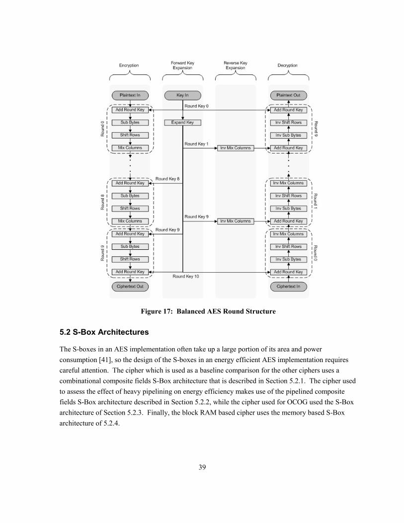
39
Figure 17: Balanced AES Round Structure
5.2 S-Box Architectures
The S-boxes in an AES implementation often take up a large portion of its area and power
consumption [41], so the design of the S-boxes in an energy efficient AES implementation requires
careful attention. The cipher which is used as a baseline comparison for the other ciphers uses a
combinational composite fields S-Box architecture that is described in Section 5.2.1. The cipher used
to assess the effect of heavy pipelining on energy efficiency makes use of the pipelined composite
fields S-Box architecture described in Section 5.2.2, while the cipher used for OCOG used the S-Box
architecture of Section 5.2.3. Finally, the block RAM based cipher uses the memory based S-Box
architecture of 5.2.4.

40
5.2.1 Logic Based Composite Field S-Box Architecture
Logic based composite field S-box designs are fairly commonly used in both ASIC and high
throughput FPGA based AES implementations. Recall from Section 2.1.2 that the SubBytes and
inverse SubBytes functions are comprised of two operations each, the multiplicative inverse in GF(28)
followed by an affine transform for the former, and the inverse of the affine transform followed by
the multiplicative inverse in GF(28) for the latter. Also recall, from Section 2.1.8, that multiplicative
inversion in GF(28) can be performed more efficiently using an isomorphic composite field which has
been built iteratively from lower order fields, though this requires performing an isomorphic
mapping, represented by δ(x), between differing field representations.
The composite field architecture was implemented almost as it was described in Section 2.1.8. To
decease the critical path though the S-Box, the inverse affine transform and isomorphic mapping were
combined into one operation for use in the inverse S-Box and the affine transform and inverse
isomorphic mapping were combined for use in the forward S-Box. This technique, also used by [34]
and [13], can be seen in Figure 18.
Figure 18: Combined Affine and Isomorphic Mapping Composite Field S-Box
Equation sets (17) and (18) show the equations for each of the bits of AT-1
δ(x) and ATδ-1
(x).
Recall that δ(x) and δ-1
(x) were defined in equation sets (9) and (10) in Section 2.1.8.
(17)
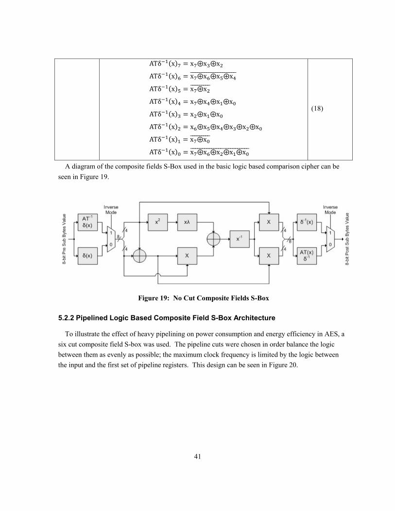
41
(18)
A diagram of the composite fields S-Box used in the basic logic based comparison cipher can be
seen in Figure 19.
Figure 19: No Cut Composite Fields S-Box
5.2.2 Pipelined Logic Based Composite Field S-Box Architecture
To illustrate the effect of heavy pipelining on power consumption and energy efficiency in AES, a
six cut composite field S-box was used. The pipeline cuts were chosen in order balance the logic
between them as evenly as possible; the maximum clock frequency is limited by the logic between
the input and the first set of pipeline registers. This design can be seen in Figure 20.

42
Figure 20: Six Cut Composite Fields S-Box
5.2.3 Opportunistically Gated Composite Fields S-Box Design
To evaluate the effects of OCOG, the Opportunistic Combinational Operand Gating technique
discussed in Section 4.2.5 was applied to the pipelined composite fields S-Box.
The goal of opportunistic gating in the composite fields S-Box is to gate out hardware which is
required for only the forward or inverse SubBytes operation when the opposite function is performed.
As was seen in Figure 18, the δ(x) and ATδ-1
(x) functions are used only in the forward SubBytes
function, while the AT-1
δ(x) and δ-1
(x) functions are used only in the inverse function. This means
that combinational gating can be applied to both the pre and post multiplicative inverse sections of the
design, using the inverse mode signal for gating purposes. The pre multiplicative inverse section was
examined first.
The first step of performing opportunistic combinational gating in the pre multiplicative inverse
section of the six cut composite fields S-Box was to assess the post technology mapped design for
LUTs to gate. The post mapped hardware structure of the pre multiplicative inverse section can be
seen in Figure 21. This diagram shows all of the hardware from the input of the S-box all the way
until the first pipeline cut after the first multiplexor. The eight bits of S-Box input as well as the
inverse mode signal are on the left of the diagram while the eight bits output by the pre multiplicative
inverse multiplexor can be seen on the right.

43
Figure 21: Pre Multiplicative Inverse Technology Map
Each LUT in the diagram is surrounded by a box. Lookup tables that contain AND gates are used
to perform the multiplexing feature and cannot be further gated since they are used in both the
forward and inverse operation of the S-Box. Lookup tables that contain only XOR logic, on the other
hand, can be gated provided that they have an unused input available and that their output is not used
in both the forward and inverse SubBytes functions. Figure 22 shows the pre multiplicative inverse
technology map diagram again with the LUTs of interest labeled and all but the signals important for
gating removed for easier analysis.
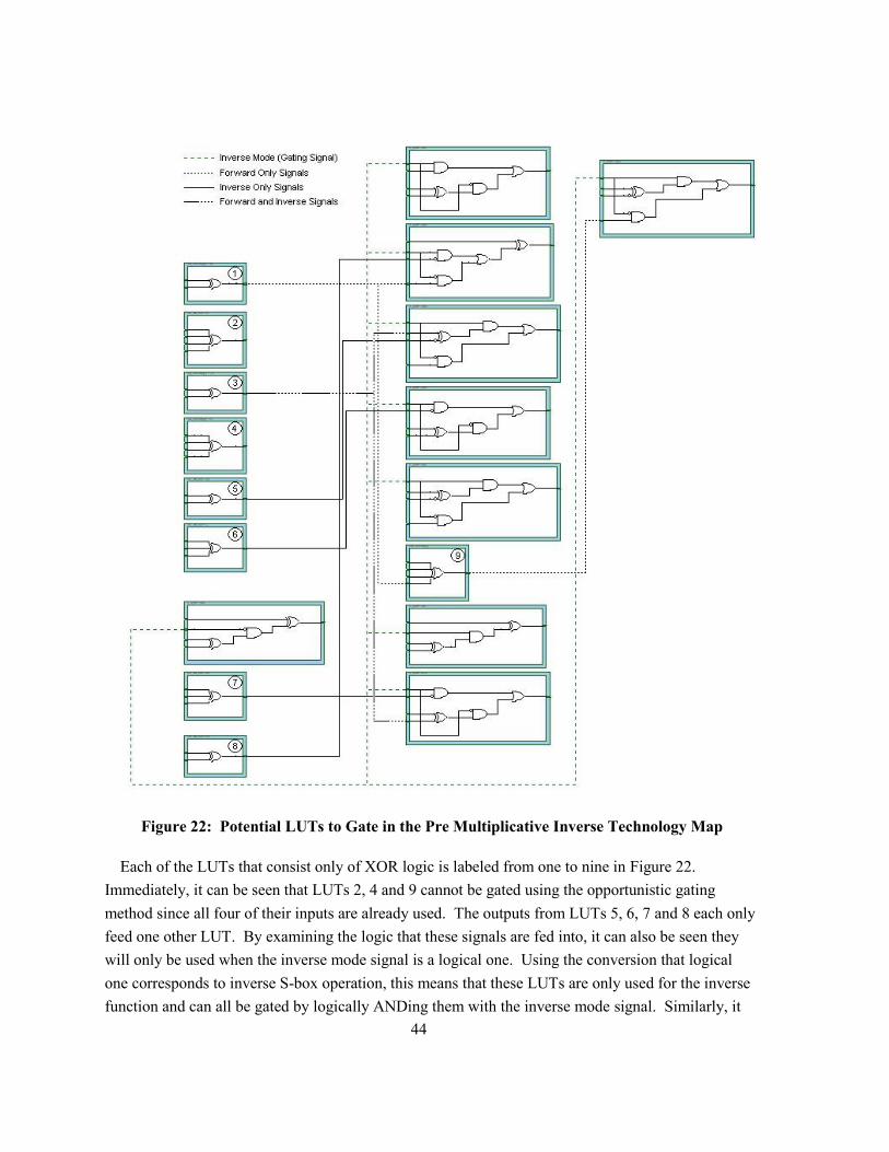
44
Figure 22: Potential LUTs to Gate in the Pre Multiplicative Inverse Technology Map
Each of the LUTs that consist only of XOR logic is labeled from one to nine in Figure 22.
Immediately, it can be seen that LUTs 2, 4 and 9 cannot be gated using the opportunistic gating
method since all four of their inputs are already used. The outputs from LUTs 5, 6, 7 and 8 each only
feed one other LUT. By examining the logic that these signals are fed into, it can also be seen they
will only be used when the inverse mode signal is a logical one. Using the conversion that logical
one corresponds to inverse S-box operation, this means that these LUTs are only used for the inverse
function and can all be gated by logically ANDing them with the inverse mode signal. Similarly, it

45
can be seen that the output from LUT 1 will only be used when the inverse mode signal is a logical
zero, and it can be gated by logically ANDing with the inverse of the inverse mode signal. At first
glance, it appears that LUT 3 can also be gated since it only uses two of the LUTs available inputs,
but this is not the case. The signal output from LUT 3 is a common sub expression used in the both
the forward and reverse SubBytes functions and cannot be gated since it is required in both cases.
To implement opportunistic combinational gating on the pre multiplicative inverse section, the
revised equation sets for the combined inverse affine transform with isomorphic mapping and
isomorphic mapping given in (19) and (20) were used. In these equations, the inverse mode signal is
defined as IM, and the gated LUTs are defined by the PreGate signals.
(19)
(20)

46
The exact same process was used to implement opportunistic combinational gating in the post
multiplicative inverse section of the design. The equations shown in sets (21) and (22) define how
gating was applied. The PostGate signals define the LUTs that are gated in the post multiplicative
inverse section, while IM again is the inverse mode signal.
(21)
(22)
The post technology map hardware structure of both the gated pre and post multiplicative inverse
sections were examined to verify that gating was applied as expected.
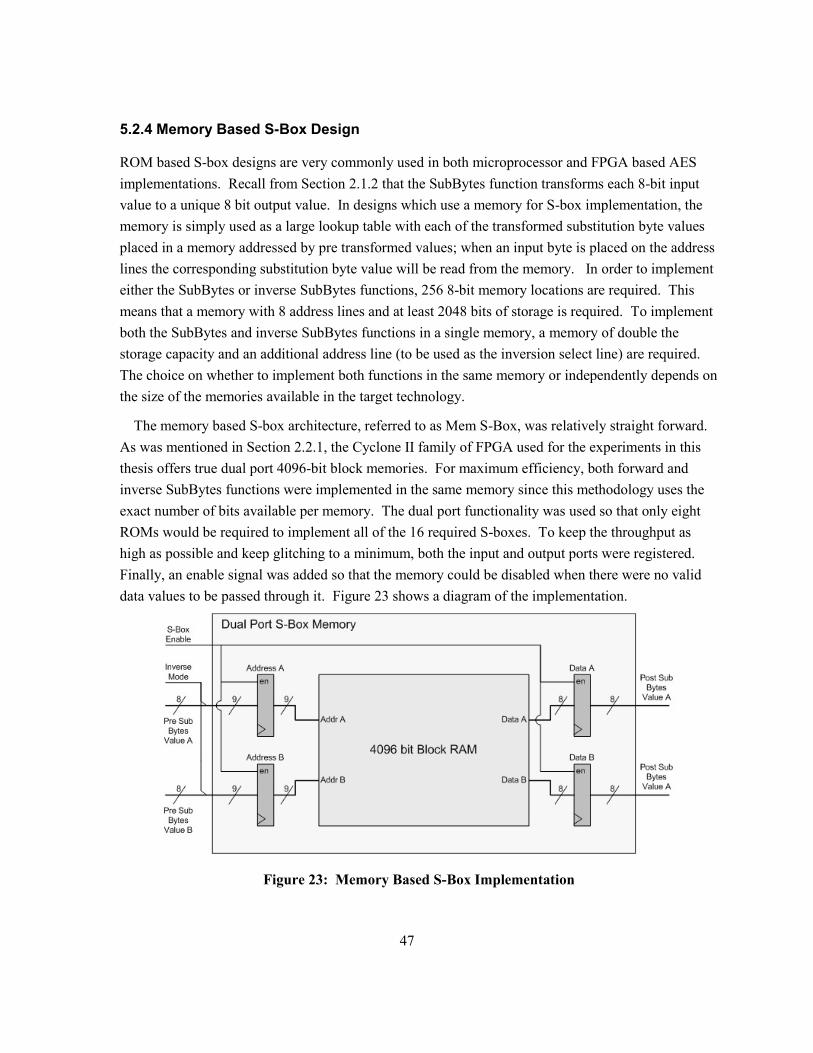
47
5.2.4 Memory Based S-Box Design
ROM based S-box designs are very commonly used in both microprocessor and FPGA based AES
implementations. Recall from Section 2.1.2 that the SubBytes function transforms each 8-bit input
value to a unique 8 bit output value. In designs which use a memory for S-box implementation, the
memory is simply used as a large lookup table with each of the transformed substitution byte values
placed in a memory addressed by pre transformed values; when an input byte is placed on the address
lines the corresponding substitution byte value will be read from the memory. In order to implement
either the SubBytes or inverse SubBytes functions, 256 8-bit memory locations are required. This
means that a memory with 8 address lines and at least 2048 bits of storage is required. To implement
both the SubBytes and inverse SubBytes functions in a single memory, a memory of double the
storage capacity and an additional address line (to be used as the inversion select line) are required.
The choice on whether to implement both functions in the same memory or independently depends on
the size of the memories available in the target technology.
The memory based S-box architecture, referred to as Mem S-Box, was relatively straight forward.
As was mentioned in Section 2.2.1, the Cyclone II family of FPGA used for the experiments in this
thesis offers true dual port 4096-bit block memories. For maximum efficiency, both forward and
inverse SubBytes functions were implemented in the same memory since this methodology uses the
exact number of bits available per memory. The dual port functionality was used so that only eight
ROMs would be required to implement all of the 16 required S-boxes. To keep the throughput as
high as possible and keep glitching to a minimum, both the input and output ports were registered.
Finally, an enable signal was added so that the memory could be disabled when there were no valid
data values to be passed through it. Figure 23 shows a diagram of the implementation.
Figure 23: Memory Based S-Box Implementation

48
As can be seen in the diagram, a single clock enable is used to control both the synchronous inputs
and outputs of the memory. This means that the S-box ROM must always be kept active for at least
two clock cycles at a time to ensure that data clears the memory outputs if data retrieval is necessary.
5.3 MixColumns Designs
The MixColumns component is also considered to be an important part of the AES cipher. Sections
5.3.1 and 5.3.2 discusses the basic logic based and pipelined logic based MixColumns architectures
used while Section 5.3.3 adds OCOG to the pipelined version.
5.3.1 Logic Based MixColumns Design
While there have been many different logic based MixColumns implementation strategies proposed,
the common substructure sharing one introduced first by Satoh and Morioka [12] and later used by
Zhang [13] and Good [34] is of the most interest for energy efficient design. This design strategy
elegantly uses common substructure sharing to minimize the amount of specialized hardware required
for forward and inverse MixColumns operation, and is easily pipelined to increase throughput. The
way that this common substructure is obtained is by factoring out common terms in the matrix
multiplication introduced in equations (7) and (8) in Section 2.1.4. The factored form of the
MixColumns and InvMixColumns equations, as presented by Satoh and Morioka in [12], can be seen
in equations (23) and (24) respectively.
(23)
(24)

49
Equation sets (23) and (24) show how both forward and inverse MixColumns operations can be
performed using simple constant multiplication in GF(28) and how common substructures can be
shared between the two. In fact, the entirety of the MixColumns structure defined in equation (23) is
contained in the InvMixColumns Structure of equation (24), allowing its hardware to be used for both
operations. These equations also show that both the forward and inverse MixColumns operations can
be performed using a series of constant multiplications in GF(28) on selected bytes of input column
and XORing the results. To implement forward MixColumns, only constant GF(28) multiplication by
two and GF(28) addition (XOR) of individual input bytes is required, while implementing
InvMixColumns only requires additional GF(28) multiplications by eight and four.
Constant multiplication in GF(28) can be performed by repeated application of the “Xtime”
function [7]. “Xtime” is constant multiplication by two in GF(28) modulo the AES irreducible
polynomial of equation (2) so named because it is the multiplication by „x‟ of a GF(28) value when
expressed in polynomial form [8]. “Xtime” is commonly expressed as it is shown in equation (25),
and can be easily implemented with only three two input XOR gates. Similarly, multiplication by
four in GF(28) can be obtained by applying “Xtime” twice, and will be referred to as “X
2time”. The
equation for “X2time” is defined in (26) and can be implemented using four two input XOR gates and
one three input XOR gate.
(25)
(26)
The structure chosen for the MixColumns hardware module was based on the one used by Good
[34] and uses both the “Xtime” and “X2time” structures discussed above. It uses the substructure

50
sharing strategy to re-use the forward MixColumns hardware for the inverse MixColumns function.
While GF(28) multiplication by two and four are performed directly based on equations (25) and (26),
multiplication by eight is performed by using the “Xtime” function again on the results of the
multiplication by four. This structure can be seen in Figure 24.
Figure 24: No Cut Substructure Sharing MixColumns
The diagram shows the logic used in the MixColumns hardware module. The s0, s1, s2 and s3
values are the four bytes of the input 32-bit column. The 2x and y terms are required for the forward
and inverse MixColumns outputs, and are the required input bytes multiplied by two and one
respectively. The bytes summed together for these terms correspond directly to the terms in equation
(23). The 4w and 8z terms on the other hand, are only required by the inverse MixColumns operation
and are the required input bytes multiplied by four and eight with the bytes summed corresponding
directly to the additional terms in equation (24). The final block in both the forward and inverse
MixColumns paths is the operation‟s sum of products.
5.3.2 Pipelined Logic Based MixColumns Design
A single cut version of this design was implemented for use in the designs examining the impact of
pipelining can be seen in Figure 25. A single pipeline cut in the middle of the design was used to
ensure that its maximum clock frequency was about the same as the combinational S-Box‟s. The
speed is limited by the logic between the set of pipeline registers and the output.
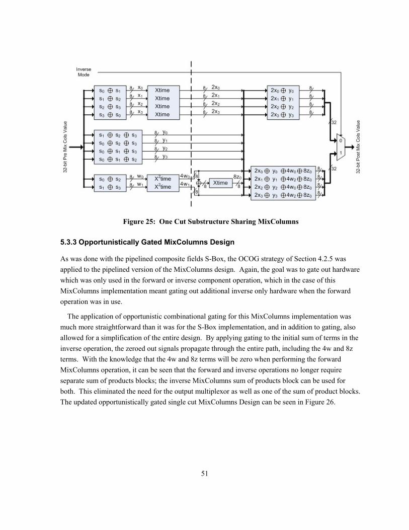
51
Figure 25: One Cut Substructure Sharing MixColumns
5.3.3 Opportunistically Gated MixColumns Design
As was done with the pipelined composite fields S-Box, the OCOG strategy of Section 4.2.5 was
applied to the pipelined version of the MixColumns design. Again, the goal was to gate out hardware
which was only used in the forward or inverse component operation, which in the case of this
MixColumns implementation meant gating out additional inverse only hardware when the forward
operation was in use.
The application of opportunistic combinational gating for this MixColumns implementation was
much more straightforward than it was for the S-Box implementation, and in addition to gating, also
allowed for a simplification of the entire design. By applying gating to the initial sum of terms in the
inverse operation, the zeroed out signals propagate through the entire path, including the 4w and 8z
terms. With the knowledge that the 4w and 8z terms will be zero when performing the forward
MixColumns operation, it can be seen that the forward and inverse operations no longer require
separate sum of products blocks; the inverse MixColumns sum of products block can be used for
both. This eliminated the need for the output multiplexor as well as one of the sum of product blocks.
The updated opportunistically gated single cut MixColumns Design can be seen in Figure 26.

52
Figure 26: Opportunistically Gated One Cut Substructure Sharing MixColumns
5.4 AES Cipher Designs
Five different cipher designs were implemented to be evaluated for power consumption and energy
efficiency. Three of these designs were intended to evaluate the effectiveness of the energy
efficiency stratagies of pipelining, OCOG, and the use of embedded block RAMs, while a fourth was
used as a baseline comparison design. The fifth design uses a combination of the energy efficiency
strategies evaluated as well as the application of clock enable gating in an attempt to develop an
energy efficient cipher. The basic comparison cipher is described first in Section 5.4.1 followed by
the strategy illustration ciphers in Sections 5.4.2, 5.4.3 and 5.4.4. Finally the Enhanced Memory
Based cipher which combines the techniques is introduced in Section 5.4.5.
5.4.1 Basic Logic Cipher
The Basic General Purpose Logic Cipher was the first design implemented and is used as a
comparison for other, more advanced designs. It is representative of a standard AES cipher where the
main goal is to ensure proper AES functionality with little to no effort applied to increase its
throughput or decrease power consumption; it does not use any of the pipelining or gating techniques
discussed in Section 4.2. The design applies one AES round per clock cycle, as it is not pipelined.
No memories were used, so the SubBytes function was implemented using the no cut composite
fields S-Box design of Figure 19, and the round keys are stored in registers. A diagram of the Basic
Logic cipher can be found in Figure 27, while the Finite State Machine (FSM) it uses to keep track of
the current round can be found in Figure 28.

53
Figure 27: Basic General Purpose Logic Cipher

54
Figure 28: Round Finite State Machine
As can been seen in Figure 27 and Figure 28, there are five inputs and two outputs on the design.
The In Data input signal is the 128 bit plain or cipher text to be operated on, while the accompanying
In Inverse Mode signal is used to indicate whether the data is to be encrypted or decrypted. The Start
which goes with these signals is used to indicate that a new valid data is being applied to the cipher
and that the round FSM should be started. The Reset signal is used to reset the FSM back to the
starting state. As can be seen in Figure 28, the design remains in Round 9 until it is started with the
Start signal. The Out Valid signal is used to indicate when the cipher operation is complete and Out
Data contains the processed data.
Figure 27 shows the flow of data through the Basic General Purpose Logic Cipher. The dotted
lines in the figure show the boundary between rounds, and all signals crossing it must be registered,
though only registers that use an enable signal or are at the input or output of the cipher have a
register pictured to reduce clutter on the diagram. The first multiplexor in the data path is used to

55
select whether the signals being supplied to the round comes from cipher input, as is required in the
initial round, or from the previous round. The first operation in the round is the AddRoundKey
function where the registered forward or inverse round key is XORed with the data depending on
whether the encryption or decryption operation is being performed. Once this is done, the SubBytes
and ShiftRows functions are applied to the data. As was discussed above, the sixteen S-Boxes are
implemented using the no cut composite fields S-Box design of Figure 19. The shift and inverse shift
rows functions can be implemented at no logic cost by simply routing the output bytes to their post
shifted positions, though two different routings are required since the forward and inverse shifts move
the bytes in different directions. Normally, an additional multiplexor would be required to implement
both directions, but by performing the forward shift rows by routing directly after the inverse
isomorphic mapping and the inverse shift rows directly after the combined affine transform / inverse
isomorphic mapping, both can be done using the S-Box‟s output multiplexor. This technique is
commonly used [34] [13] and is pictured in Figure 29. The last operation performed in the round is
MixColumns, which is implemented using the no cut common substructure sharing design of Figure
24. In parallel with MixColumns, the Final AddRoundKey function is also performed for output in
round 9, with the forward or inverse final key being applied depending on the inverse mode signal.
The Final Round Check signal indicates when the final round (round 9) has been reached and is used
to enable the data output of the design as well as to reset the valid and inverse mode signals after
cipher operation is complete.
Figure 29: Composite Fields S-Boxes with ShiftRows

56
As was mentioned above, since no memories are used in the Basic General Purpose Logic Cipher,
the pre expanded round keys must be stored in registers. For both the sets of forward and inverse
keys, a series of shift registers is loaded with the pre expanded keys for rounds 0 through 9, while a
single non-shifting register is loaded with the final round key. The series of shift registers shifts
every round that the cipher is active, that is, when not in round 9 or when the start signal is high, such
that the current round key is always output from the same register. The final round keys remain
stationary since they are only used in a single round of the cipher. A diagram of the shift register key
storage can be found in Figure 30.
Figure 30: Shift Register Key Storage
5.4.2 Piped Logic Cipher
The Pipelined Logic cipher was intended to assess the impact of applying heavy pipelining to reduce
dynamic power dissipation and improve energy efficiency. The design takes eleven clock cycles per
round, and thus can process eleven data values simultaneously and will likely achieve a very high
throughput. Like the Basic Logic cipher, no memories were used so this design also requires a
composite fields SubBytes implementation and registered key storage. In this case, the SubBytes
function was implemented using the six cut composite fields S-Box design of Figure 20 while the
same shift register key storage method shown in Figure 30 was used. Pipelining strategies were also
applied in the MixColumns component with the use of the One Cut Substructure Sharing
MixColumns design of Figure 25. A diagram of the Gated Pipeline General Purpose Logic Cipher
can be found in Figure 31.

57
Figure 31: Pipelined General Purpose Logic Cipher

58
The biggest change to the Pipelined General Purpose Logic Cipher from the basic design, other
than the addition of pipeline registers, is the more advanced control structure required to manage the
processing of eleven data values per round. The biggest complexity is making sure that round
dependent operations, such as adding a round key or enabling the output section of the design, are
applied correctly to all eleven data values. Using the case of round key application as an example,
care must be taken to ensure that the correct round key is used for all eleven values and that the round
key does not change until the final value has passed the AddRoundKey stage. To manage the flow of
data through each round, a second FSM in addition to the round FSM of Figure 28 is required. This
Control FSM is pictured in Figure 32. As can be seen in the figure, the Round FSM is only enabled
once per round, in state 0, to ensure that the proper round is used by the input multiplexor in stage 1
of the cipher. Similarly, the key storage shift registers are only enabled once per round in state 1 to
ensure that the correct round key is applied in stage 2 of the cipher. Finally, the Final Round Check
signal is enabled once per round in state 9 so that output section of the design is enabled instead of the
MixColumns section for all eleven data values in their final round through the cipher. As was the
case for the Basic General Purpose Logic Cipher, the Final Round Check signal is also used to reset
the valid and inverse mode signals after cipher operation is complete.
Figure 32: Pipelined General Purpose Logic Cipher Control FSM

59
Pipelining the design also means that a single additional input is required. A valid bit signal now
accompanies each of the input data values. Recall that in the non-pipelined version only the start
input was required since the design could only handle one data value per run of the cipher. Now that
eleven data values can be processed per cipher run, a valid bit is needed for each, in addition to the
start input which indicates the start of a cipher run.
5.4.3 OCOG Logic Cipher
The OCOG Logic cipher was intended to assess the impact of applying the Operational
Combinational Operand Gating strategy in addition to pipelining to reduce dynamic power dissipation
and improve energy efficiency. The design is identical to the Pipelined Logic cipher in every way
other than the fact that it uses the OCOGed S-Box and MixColumns architectures of Sections 5.2.3
and 5.3.3 instead of the pipelined only ones used previously.
5.4.4 Basic Memory Based Cipher
The Basic Memory Based cipher was intended to analyze the effect of using embedded memory
blocks in the design on power consumption and energy efficiency. It is representative of an AES
design which uses block RAMs for S-box and expanded key storage. Though the design does use
memories efficiently and has some naturally occurring pipelining due to the use of block RAMs with
synchronous inputs and outputs, none of the gating or heavy pipelining techniques were used to
attempt to further reduce the power consumption. Because of the natural pipelining, the design takes
three clock cycles per round, and can process three data values simultaneously. The Memory Based
S-Box Implementation of Figure 23 was used to perform the SubBytes function while the No Cut
Substructure Sharing design of Figure 24 was used to perform the MixColumns function. A diagram
of the Basic Memory Based Cipher can be found in Figure 34, while its control FSM can be found in
Figure 33. Like the previous designs, it uses the Round FSM of Figure 28 to keep track of the current
round.
Figure 33: Basic Memory Based Cipher Control FSM

60
Figure 34: Basic Memory Based Cipher

61
The most noticeable difference in the between the Basic Memory Based Cipher and the previous
general purpose logic designs that can be seen in Figure 34 other than the use of memories for S-
Boxes is the re-arrangement of the AddRoundKey section to also include the ShiftRows operation.
Recall that the general purpose logic designs of Sections 5.4.1 and 5.4.3 performed the ShiftRows
operation before the output of the SubBytes component to avoid requiring a second multiplexor for
the simple shift by routing. Since the output of both the forward and inverse S-Boxes come from the
same memory in the Basic Memory Based Cipher, this is no longer an option. In this case, the
application of ShiftRows is now combined with the AddRoundKey function. The input to the
AddRoundKey function is shifted in both the forward and inverse directions, then XORed with the
Round keys which have also been shifted in the appropriate direction. The round key selector
multiplexor then occurs after the application of the round key instead of before, as was previously the
case.
In addition to using memories for the application of the SubBytes function, the Basic Memory
Based Cipher also uses memories to hold all pre expanded forward and inverse keys for rounds 1
through 9. As can be seen in Figure 33, the memories are enabled in the final state of the round, state
2, and the initial state of the round, state 0. The addresses of the required forward and inverse keys
are applied to the memories in state 2 so that the read action can occur during state 0 and the keys will
be ready at the memory outputs in state 1 when they are first required for the round. This means that
the read operation for a given round key must start in the final state of the previous round. For
example, the read operation to retrieve the keys for round 1 would start at the end of round 0 and the
read operation to retrieve the keys for round 9 would start at the end of round 9. Since round 9 is the
final round, the memory would be disabled during this round. The address scheme used for the
memories is a simple binary encoding of the round when the read is taking place. A diagram of the
memory based key storage can be found in Figure 35. Recall from Section 2.2.1 that each Cyclone II
block RAM can have a maximum of 32 bits, so eight block RAMs are required to store both the
forward and inverse round keys.
The initial and final round keys are stored separately in registers. Since the read for each set of
round keys must be started in the previous round, the initial round keys cannot be stored in the
memories because they would not be accessible in time for the initial round. Also, recall that the final
round requires the application of two round keys. Since only one round key can be retrieved from a
memory at once, the final round keys also must be stored outside of the block RAMs. Fortunately,
the initial forward key and the final inverse key are the same, as are the initial inverse key and final
forward key, so only two 128 bit registers are required for all of the initial and final round keys. The
initial and final round key storage registers can be seen in Figure 36.

62
Figure 35: Basic Memory Based Cipher Memory Key Storage
Figure 36: Initial and Final Key Storage for Memory Based Cipher
5.4.5 Enhanced Memory Based Cipher
The Enhanced Memory cipher used a combination of all of the applicable energy efficiency strategies
of Section 4.2 in an attempt to create the most energy efficient AES cipher possible. The goal for
this design was to achieve high energy efficiency by focusing on minimizing power wherever
possible through the use of memory and gating techniques while still keeping the maximum
throughput possible. The design takes four clock cycles per round, and thus can process four data
values simultaneously. Like the Basic Memory Based Cipher, this design uses block RAMs to
implement both the SubBytes function and expanded key storage. In this case however, the
Opportunistically Gated One Cut Substructure Sharing design of Figure 26 was used for the
MixColumns component to get the low power benefits of further pipelining and combinational gating.
This design also takes advantage of the enable line on the Memory Based S-Box Implementation of
Figure 23 to reduce unnecessary usage of the S-Box Memories as part of the clock enable gating
strategy. Finally, The Enhanced Memory cipher uses an enhanced Gray style memory encoding to

63
reduce the activity of the key expander memory address encoder and save power. A diagram of the
cipher‟s control FSM can be seen in Figure 37 while the cipher itself can be seen in Figure 38. The
design‟s memory based expanded key storage with new encoding can be seen in Figure 39.
Figure 37: Gated Pipeline Memory Based Cipher Control FSM
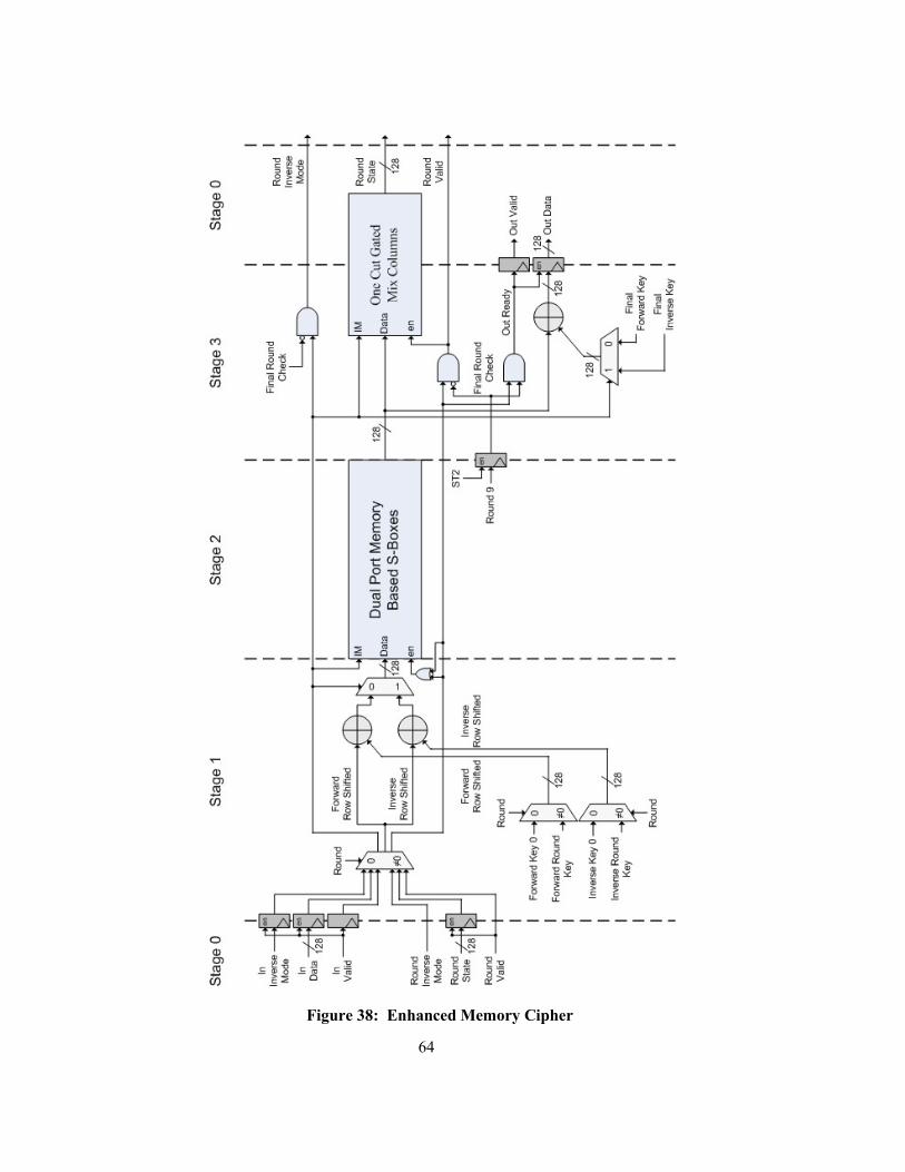
64
Figure 38: Enhanced Memory Cipher

65
Figure 39: Gated Pipeline Memory Based Cipher Memory Key Storage
5.5 Full AES with Key Expansion Design
The final design to be discussed is the Full AES with key expansion implementation. The goal of this
design was simply to develop a complete AES implementation that is as energy efficient as possible.
As was planned in Section 4.3, this design is based on the most energy efficient cipher that was
evaluated, the Enhanced Memory cipher. To retain as much of the energy efficiency of this cipher as
possible, only minor changes were made to its design to accommodate the addition of a key expander;
the key expander was constructed to fit the existing high efficiency cipher.
5.5.1 Application of Economic Key Expansion
As was discussed in Section 4.2.3, the principles of economic key expansion were used to help
make the Full AES implementation as energy efficient as possible. The key expander expands keys
in parallel with cipher operation as is done with most high throughput designs, but also saves the
expanded key for future use as is done with most low power designs. Separate keys are expanded for
each of the concurrent data streams but keys do not need to be expanded for unused data streams, and
inverse key expansion does not have to be performed for data streams that will not be using the
decryption function.
The use of these economic key expansion principles means that four operations can be performed
by the Full AES design, either individually or in various combinations. The Full AES design can
perform Encryption, Decryption, Forward Key Expansion and Inverse Key Expansion. Any of the
operations can be performed on their own to minimize the amount of energy they consume, but of
course, some operations are dependent on others. Both Encryption and Inverse Key Expansion
require the expanded forward key, so Forward Key Expansion must be performed before or at the
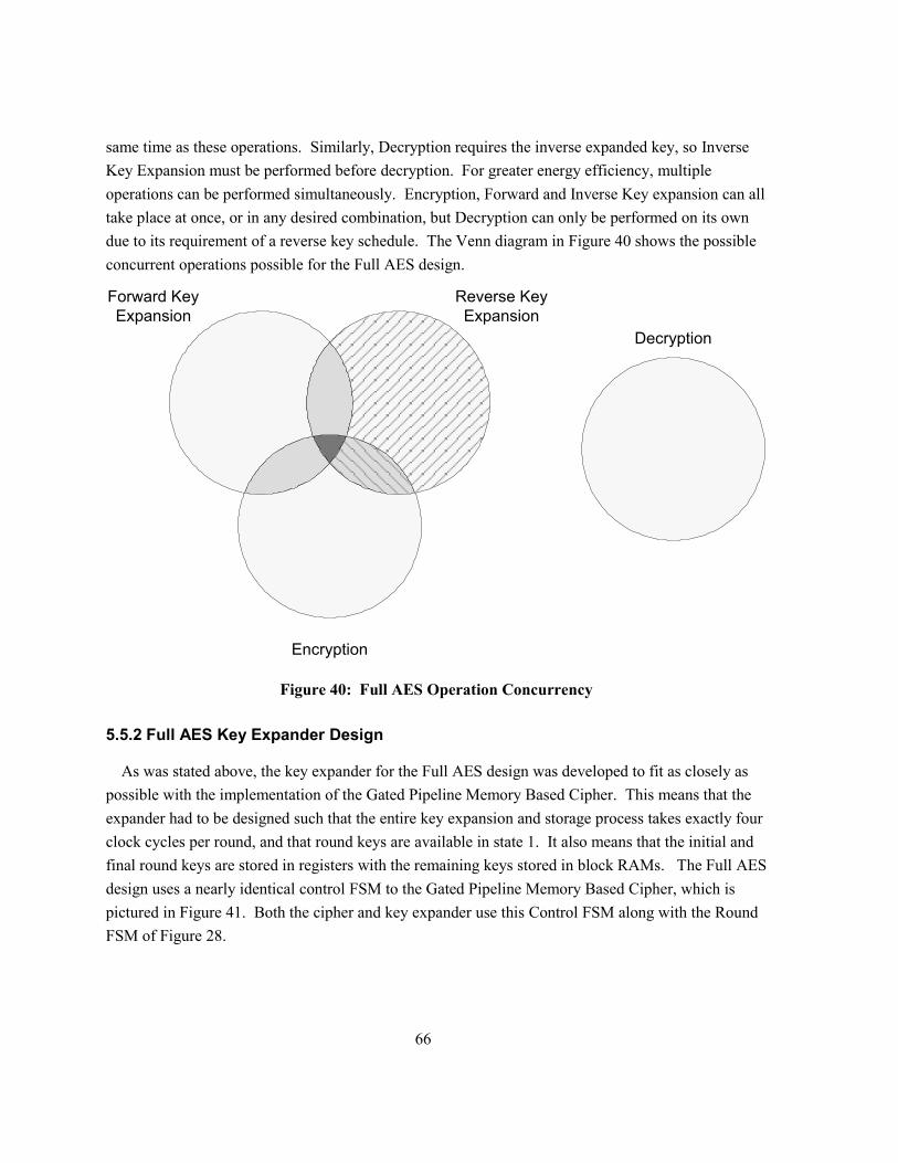
66
same time as these operations. Similarly, Decryption requires the inverse expanded key, so Inverse
Key Expansion must be performed before decryption. For greater energy efficiency, multiple
operations can be performed simultaneously. Encryption, Forward and Inverse Key expansion can all
take place at once, or in any desired combination, but Decryption can only be performed on its own
due to its requirement of a reverse key schedule. The Venn diagram in Figure 40 shows the possible
concurrent operations possible for the Full AES design.
Figure 40: Full AES Operation Concurrency
5.5.2 Full AES Key Expander Design
As was stated above, the key expander for the Full AES design was developed to fit as closely as
possible with the implementation of the Gated Pipeline Memory Based Cipher. This means that the
expander had to be designed such that the entire key expansion and storage process takes exactly four
clock cycles per round, and that round keys are available in state 1. It also means that the initial and
final round keys are stored in registers with the remaining keys stored in block RAMs. The Full AES
design uses a nearly identical control FSM to the Gated Pipeline Memory Based Cipher, which is
pictured in Figure 41. Both the cipher and key expander use this Control FSM along with the Round
FSM of Figure 28.
Encryption
Decryption
Forward Key
Expansion
Reverse Key
Expansion

67
Figure 41: Full AES Control FSM
In addition to the input signals required by the cipher and FSM of the Full AES design, four more
input signals are required that are used only by the key expander. The most obvious of these is, of
course, is the 128 bit input key to be expanded. The Activate Key Expander signal, pictured in Figure
42, is used to enable components of the key expander for an entire run of the cipher using the Exp En
signal. As can been seen in the control FSM of Figure 41, the updating of the round constant and the
enabling of initial round check signals are both dependant on the Exp En signal. The final two key
expander input signals, In Expand Forward and In Expand Inverse, are used to indicate that the key
for the current data stream should be forward or inverse expanded. If the In Expand Forward signal is
set high, the accompanying key will be forward expanded for the current data stream. If In Expand
Inverse signal is set high, the key will be Inverse expanded for the current data stream. Of course
both of these signals can be used at the same time if both forward and inverse key expansion are
required.
Figure 42: Activate Key Expander Input

68
A diagram showing the Full AES designs key expander can be seen Figure 43. There are two main
data paths through the key expander that are activated for either forward or inverse key expansion as
well as a common feedback path that is used for both. The forward key expander path goes from the
Least Significant Word (LSW) of Input Key or looped Temp word from the previous key through the
SubBytes, RotWord, Rcon application functions then through the word wise XORing with the
previous key and finally into the forward key storage memory or final key storage register. The
previous 128 bit key that is word wise XORed with the current key words are obtained from the set of
the initial key storage registers for the calculation of round key 1 during round 0, or from the
feedback path for the calculation of the other round keys. The common feedback path is used both
for XORing the previous key with the current key words, as well as for supplying the forward keys
for the inverse keys to be calculated from. The common portion of the feedback path starts at the
output of the forward key storage memory and includes one register inserted so that the feedback
value is available at the proper time. The Most Significant Double Word (MSDW) from the common
portion of the feedback path is available to be XORed with the first half of the current forward key in
Stage 2, while the Least Significant Double Word (LSDW) is registered again for application in Stage
3. The inverse key expansion path starts directly after the common feedback portion where the
previously calculated forward round key is fed into the InvMixColumns function. Once
InvMixColumns has been applied, the inverse key expansion path ends with the inverse key being
stored in the inverse key storage memory.
The expand forward and inverse control paths beginning with the Expand Forward and Expand
Inverse input signals discussed above control which of these data paths are active at any given time.
As expected, the expand forward signal path controls the forward key expansion data path, while the
expand inverse signal path controls the inverse key expansion data path. Both control paths can cause
the common feedback path to be activated.

69
Figure 43: Full AES Key Expander
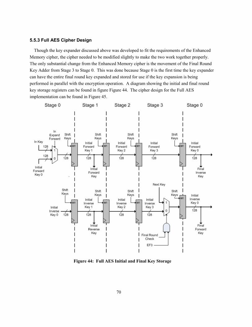
70
5.5.3 Full AES Cipher Design
Though the key expander discussed above was developed to fit the requirements of the Enhanced
Memory cipher, the cipher needed to be modified slightly to make the two work together properly.
The only substantial change from the Enhanced Memory cipher is the movement of the Final Round
Key Adder from Stage 3 to Stage 0. This was done because Stage 0 is the first time the key expander
can have the entire final round key expanded and stored for use if the key expansion is being
performed in parallel with the encryption operation. A diagram showing the initial and final round
key storage registers can be found in figure Figure 44. The cipher design for the Full AES
implementation can be found in Figure 45.
Figure 44: Full AES Initial and Final Key Storage
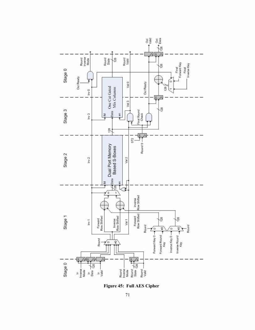
71
Figure 45: Full AES Cipher

72
Since both the final and initial keys are required by the cipher only one clock cycle after they are
available, they must be stored in registers instead of in the key storage memories with the rest of the
round keys. Since each of the four data streams needs to be able to operate independently, each one
requires its own initial and final keys. Again, since the initial forward keys are identical to the final
inverse keys and the initial inverse keys are identical to the final forward keys, only eight keys must
be stored in total to have the full set of initial and final keys for both encryption and decryption for all
streams. An initial key is stored in the upper set of key registers during round 0 whenever a forward
key is being expanded for a data stream. When the forward key expansion for the data stream reaches
round 9, a new final key is stored in the lower set of key registers. The initial and final round key
registers need to be shifted every clock cycle whenever they are in use to make sure that the keys
remained lined up with their corresponding data stream. This is accomplished through the use of the
Shift Keys signal, pictured in Figure 46.
Figure 46: Full AES Shift Keys
The Shift Keys signal of Figure 46 ensures that all of the initial and final round keys are kept in
sync with their corresponding data streams whenever they are needed while preventing unnecessary
and energy wasting shifting at other times. The keys must be kept in sync with their data values
during round 0, obviously so that the correct initial keys are applied during the initial AddRoundKey
operation and so that the proper feedback words are XORed during the initial round of key expansion,
but also so that final data streams from the previous cipher round that are still in their final round have
their final round key added properly. Similarly, the keys also need to be kept in sync during round 9
to ensure that the final round keys are applied to the correct data stream. The additional logic
included with the round 9 signal is to ensure that the key registers do not needlessly shift when the
design is in the idle state of round 9, state 0, when there is no new data value on the way. Finally, the
registers need to be kept in sync during round 1 when the key expander is in use to ensure that
feedback XORing works correctly for all of the data streams.
The remaining middle keys are all stored in key storage memories. Each of the four data streams
requires nine forward and nine inverse 128 bit keys to be stored in key storage memory. This means
that 9216 bits of memory are required: 4608 for forward keys and 4608 for inverse keys. As was the
case for the memory based cipher however, 8 4096 bit block RAMS are required in total to

73
implement these, due to the limitation of only being able to output 32 bits at once from each RAM.
As can be seen in Figure 43, both the forward and inverse key storage memories have synchronous
inputs and outputs, and use enable and write enable signals to control their operation. The use of
synchronous inputs and outputs mean that it only takes one clock cycle to write a new key into the
memory during expansion, but takes two clock cycles to retrieve a key from the memory. Key
retrieval is, of course, required during both encryption and decryption but is also required from the
forward key storage memory during forward and inverse key expansion. During forward key
expansion, the most recently expanded key needs to be fed back into the expander to expand the next
forward key, while the inverse key expander requires previously expanded forward round keys to
transform into inverse round keys. Key retrieval is performed regardless of whether a write
operation is being performed due to the read during write functionality of the block RAMs. This
functionality is what allows the forward key storage memories to be used as feedback elements during
forward key expansion, and also allows for the possibility of performing encryption and/or inverse
key expansion at the same time as forward expansion. Writing a key to the memory is only required
during the key expansion process. Figure 47 shows the enable signals that are used for the forward
and inverse key storage memories.
Figure 47: Full AES Memory Key Storage Enable Signals
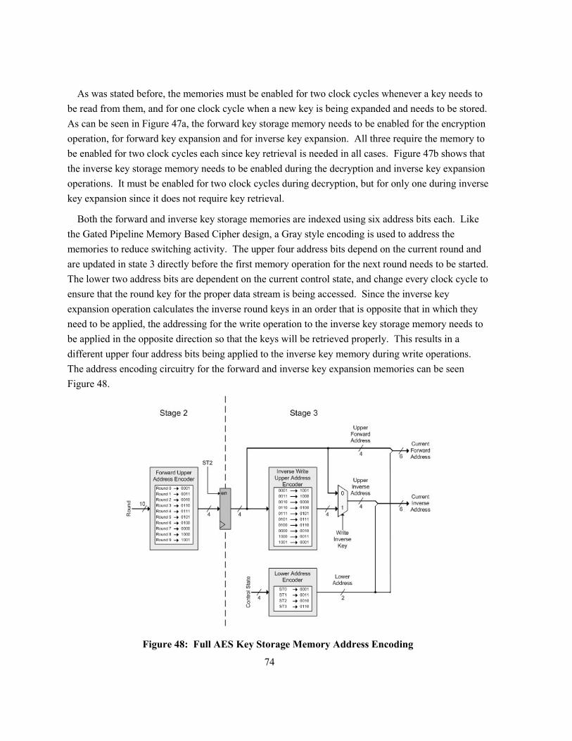
74
As was stated before, the memories must be enabled for two clock cycles whenever a key needs to
be read from them, and for one clock cycle when a new key is being expanded and needs to be stored.
As can be seen in Figure 47a, the forward key storage memory needs to be enabled for the encryption
operation, for forward key expansion and for inverse key expansion. All three require the memory to
be enabled for two clock cycles each since key retrieval is needed in all cases. Figure 47b shows that
the inverse key storage memory needs to be enabled during the decryption and inverse key expansion
operations. It must be enabled for two clock cycles during decryption, but for only one during inverse
key expansion since it does not require key retrieval.
Both the forward and inverse key storage memories are indexed using six address bits each. Like
the Gated Pipeline Memory Based Cipher design, a Gray style encoding is used to address the
memories to reduce switching activity. The upper four address bits depend on the current round and
are updated in state 3 directly before the first memory operation for the next round needs to be started.
The lower two address bits are dependent on the current control state, and change every clock cycle to
ensure that the round key for the proper data stream is being accessed. Since the inverse key
expansion operation calculates the inverse round keys in an order that is opposite that in which they
need to be applied, the addressing for the write operation to the inverse key storage memory needs to
be applied in the opposite direction so that the keys will be retrieved properly. This results in a
different upper four address bits being applied to the inverse key memory during write operations.
The address encoding circuitry for the forward and inverse key expansion memories can be seen
Figure 48.
Figure 48: Full AES Key Storage Memory Address Encoding

75
5.6 Chapter Summary
This chapter presented the implementation details of the AES designs used in this thesis. The
individual S-Box and MixColumns components which used the various energy efficiency strategies
were given first, followed by the ciphers to be used to assess the strategies‟ effectiveness. Finally, the
implementation details of the proposed energy efficient AES design were given. The next chapter
presents the methodology and scripting tool used to evaluate energy efficiency of these designs.

76
Chapter 6
Energy Analysis Methodology
The purpose of this chapter is to describe the methodology used to assess the energy efficiency and
power consumption of the AES designs. The cipher designs presented in Chapter 5 need to be
assessed so that the effectiveness of the strategies they employ can be evaluated while the Full AES
design must be fully analyzed in terms of power and energy efficiency to evaluate how energy
efficient it is. Given the importance of having a fixed and reliable method for compiling designs for
energy efficiency and evaluating these designs, a software tool called the AES Energy Analyzer was
also developed to automate the process. The use of this tool allowed for in depth power and energy
efficiency analysis to be performed.
The chapter is laid out as follows. Section 6.1 discusses the specific objectives of the energy
analysis of the designs, while Section 6.2 discusses the exact method used to obtain energy and power
estimates. The details of the AES Energy Analyzer are given in Section 6.3.
6.1 Analysis Objectives
The overall goal of the energy analysis of an AES design is, of course, to assess the energy efficiency
of that design. This is evaluated by determining the amount of energy that each design uses during
each operation it performs.
For the purpose of this thesis, the core energy consumption is evaluated and the I/O energy
consumption is ignored. Encryption algorithm implementations such as AES are rarely implemented
by themselves on a reconfigurable platform such as an FPGA; it is much more likely that the
algorithm would be implemented as a component of a larger System on Chip design. In these
situations, the inputs and outputs of the encryption algorithm would likely be connected to other
components of the SoC design and would not go off chip. Therefore, no energy would be consumed
by the encryption component in chip I/O. Given that this is the most common usage scenario in
FPGA based designs, it makes little sense to assess the energy efficiency of the designs by including
I/O energy.
The assumption of whether a design is implemented as part of a larger SoC or on its own in an
FPGA also has an impact on how much of an effect the static power dissipation of a design will factor
into its energy efficiency. If a design is implemented on its own in an FPGA that the full amount of
energy consumed resulting from the static power of the FPGA simply being on must be considered
when evaluating energy efficiency. If a design is part of a larger SoC on the other hand, it is
reasonable to assume at the static power costs of having the FPGA powered up can be shared among
all of the operations being performed in the system. This means that the amount of static energy

77
considered when determining the energy efficiency of a design should be proportional to the amount
of FPGA resources used by the design.
To evaluate a proposed design at its highest efficiency, its energy consumption is assessed when it
is operating at the highest possible data rate. This means that the design must be run at its maximum
frequency, and that data parcels must be supplied to it immediately when it is able to accept them.
For a pipelined design, this means that every pipe stage will always be full. Inputting data parcels
whenever possible in pipelined designs leads to them operating at their maximum energy efficiency
and is a valid practice assuming that one of the non feedback modes of operation (Counter, ECB) is
being used, or that a feedback mode of operation is being used and multiple streams of data needed
processing simultaneously. For this thesis, this usage situation is referred to as normal multi-stream
operation.
It was also important to evaluate the energy consumption of the design when it is operated in the
worst case situation in which a feedback mode of operation (such as CBC) is used and only a single
stream of data is required. To assess the maximum energy efficiency of a design in this situation, it is
necessary reduce the rate at which parcels were supplied to ensure that only a single parcel of data is
being processed at any time. For this thesis, this usage situation is referred to as single-stream
operation.
In addition to evaluating the energy efficiency that a design is capable of achieving at its maximum
clock rate, it is also of interest to determine its energy efficiency at lower frequencies. Since dynamic
power dissipation and throughput are proportional to the frequency that a design is run at but static
power dissipation is not, running a design at lower frequencies will demonstrate the effect that static
power has on energy efficiency.
6.1.1 Operations Assessed for Power Dissipation and Energy Efficiency
When assessing a design for power and energy efficiency, it is important to analyze it during all of the
operations it can perform. The cipher designs can perform encryption, decryption while the Full AES
implementation can perform encryption, decryption, or any combination of key expansion functions
with or without encryption. Power dissipation and energy consumed per encryption and decryption
were assessed for the cipher and Full AES designs. The combinations of key expansion operations
and encryption operations which were assessed were indicated in Figure 40 by having no fill pattern.
Unfortunately, due to the way reverse key expansion was performed, it was not possible to reliably
use the methodology described in Section 6.2 to determine the energy consumed by reverse key
expansion when forward key expansion was not simultaneously done. These operation combinations
which were not evaluated were indicated in Figure 40 by having a hatching fill pattern.
In addition to the above operations, the AES cipher and Full AES design also had the power
dissipated when in an idle state assessed. Assessing the power usage while the devices were idle

78
made more sense than evaluating the energy consumption since no task is being performed; it makes
little sense to evaluate the amount of energy consumed per operation if technically no operation is
being performed. Since it is common in many applications for hardware to sit idle and ready for data,
it was important to determine how much power the designs would require in this state.
6.2 Methodology to Assess Energy Efficiency and Power Consumption
For this thesis, energy efficiency analysis was performed based on power consumption data obtained
by simulating the design in operation. This method involves logging the transitions of internal signals
of a design during post place and route simulation and is the most accurate way to estimate power
consumption of a design using the tools discussed in Section 2.4 [19].
Evaluating the power consumption of a design is the first step in determining its energy efficiency.
To evaluate the designs over a large input range, repeated simulation of each of the operations
discussed in Section 6.1.1 was performed using randomly generated input values. For a given
simulation, only a single type of operation was tested to ensure that all of the power consumed by the
device during simulation was because of the current operation of interest. Though it was not
absolutely necessary because of the large number of each type of test performed, the same set of
random input values were used for tests of the same operations on different designs to ensure a fair
comparison between the cipher designs. As an example, to determine the power consumption while
performing encryption, a simulation of the design repeatedly performing encryption on a random set
of plaintexts would be run. This same set of plaintexts in the same order would be used to evaluate
the power consumption of the encryption function of all of the other AES cipher designs.
Once the power consumption for a design performing a given operation was determined, the
amount of energy used per operation could be calculated. Based on equation (12), the energy used
per operation is given by equation (27) below:
(27)
Where EPerOp is the energy per operation, Pop is the average power dissipation while the operation is
being performed, and top is the time it takes for the operation to complete. In many of the designs that
were evaluated, the use of pipelining meant that it was often possible to have multiple operations
being performed simultaneously. In order to factor in this possibility, equation (27) was modified to
equation (28) as follows:
(28)
Where Tsim is the clock period that the operation is being simulated at, Ncycrun is the number of
cycles that it takes for one operation to be completely run through the design, and Noprun is the
number of operations which can be concurrently run at the same time. The product of Tsim and

79
Ncycrun gives the amount of time taken to run through the algorithm, while division by Noprun
accounts for the fact that Noprun operations were performed during this time. Noting the similarities
between equation (28) and equation (16) from Section 4.2.1, the energy per operation could be given
in terms of throughput:
(29)
Where Nbitsop is the number of bits processed per operation, and TPsim is the throughput for the
design at the frequency it was simulated at. Equation (29) was used to calculate the energy per
operation for all of the operations discussed in Section 6.1.1.
6.3 AES Energy Efficiency Analyzer Script
The AES Energy Efficiency Analyzer Script, as its name suggests, is a software tool which was
developed to simplify the process of performing power and energy analysis on the AES designs
which were developed. It uses the repeated operation simulation methodology described in Section
6.2 to determine the amount of energy used per operation for each design according to Section 6.1.1.
According to the goals discussed in Section 6.1, the script attempts to assess the amount of energy
consumed by the FPGA core at the full range of frequencies that the design is capable of running at.
The script was developed using Perl and Tcl programming and Altera Quartus II FPGA design
tools. Tcl was used to interface with the Quartus II tools since Quartus II has integrated Tcl support.
Perl was used for the majority of script, including setup processing and results calculation as well as
output formatting. Perl was chosen for these tasks over Tcl since Perl is much easier to script with
and has powerful text parsing abilities.
6.3.1 Operational Flow of Script
The AES Energy Efficiency Analyzer Script automates the entire process of evaluating the power
consumption and energy efficiency of AES designs. It uses the Quartus II Synthesis and Fitter tools
to synthesize and place and route the design based on the input VHDL code. Based on the set of
input values supplied, it will also generate a test bench file for each of the operations to be evaluated
at each of the frequencies of interest then runs them on the post place and route designs using the
Quartus II Simulator. This will generate the SAF files required for power analysis, which it will then
perform using the Quartus II PowerPlay Power Analyzer. Finally, the amount of energy consumed
per operation is calculated, and output in Comma Separated Value (CSV) format along with the
amount of power dissipated and other design data. Figure 49 shows the general flow of operation of
the script.

80
Figure 49: Flow of AES Energy Efficiency Analyzer
The Project Setup, Compilation, Operation Simulation, and Design Analysis processes performed
by the script are discussed in more detail in the following Sections.
6.3.2 Project Setup
The purpose of the Project Setup process is, as its name implies, to do the initial generic setup tasks
required so that the rest of the script can be performed. The main function performed is the retrieval
of the information required to run energy assessment from the AES Energy Project (AEP) file. The
AEP file is a file that contains all the project, device and design information required by the script for
an AES design or component.
Project information is the information required for compilation of the project and includes the name
of the project as well as lists of all of the VHDL and memory initialization files required for the
design. The VHDL files are required; they contain the hardware description of the design. One of
the VHDL files must have the same name as the project name, and will be used as the top level entity
of the design. The memory initialization files contain the initial values for the memories in a design
and are only required for designs that use S-Box or pre expanded key storage ROMs. If they are not
required, the list will be left blank.

81
Device information is the information that defines the hardware the design will be implemented on
and includes the device family and name, as well as, if required, the IO standard which will be used
for fast clock input. The Altera EP2C35F672C6 device from the Cyclone II family was used for all
designs assessed in this thesis.
Design information is the information about the particular design which is being assessed. It is the
information which defines the timing of the design. Included in the design information is number of
identical rounds in the design, the number of clock cycles required by each identical round, the
number of modified final rounds in the design, and the number of clock cycles required by each
modified final round. Using the AES structure used in this thesis, the AES cipher and Full AES
designs all contain nine identical rounds and one modified final round which may contain a different
number of clock cycles from the identical rounds depending on the specific design.
6.3.3 Compilation
The goal of the Compilation process is to synthesize and place and route the design that is being
evaluated on the specified device while using all of the available low power options. The script uses
the Quartus II Integrated Synthesizer for synthesis and the Quartus II Fitter for placement and routing.
As was discussed in Section 2.4.1, signal activity data from the design is required to perform power
driven placement and routing. This means that two separate compilations must be performed: A
preliminary compilation without using low power options followed by a power driven compilation
using the signal activity data obtained by running a simulation on the first compilation. Figure 50
shows the flow of the compilation process.
The preliminary compilation must be performed first and can be seen at the top of Figure 50. This
compilation is made with the standard fitter effort, and balanced speed goal options set. The first step
in the preliminary compile is to compile the design without any timing constraints. A compilation
such as this with no timing constraints will often yield a design that cannot be simulated at or even
near the maximum reported frequency due to the wide distribution of setup and hold time
requirements of the input pins, but it is important to perform to get a realistic target maximum
frequency for the design. The setup and hold time restrictions from the initial preliminary compile
are examined to see if it is possible to find a toggle time which will work for all of the design‟s pins.
If a possible common toggle time exists, the preliminary compilation is complete, if not, the design
must be recompiled with timing constraints. Equation set (30) shows the minimum acceptable
maximum frequency and maximum acceptable setup and hold time values which are used as
constraints. FmaxC is the constrained maximum frequency while Fmaxi is the initial maximum
frequency reported after compilation. The thC and tsuC values are the hold and setup time
requirements respectively. Finally, TminC is the inverse of the maximum frequency constraint.
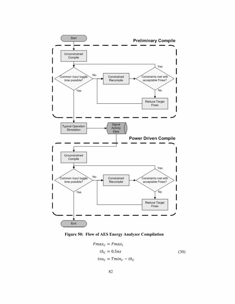
82
Figure 50: Flow of AES Energy Analyzer Compilation
(30)

83
After the recompile is complete, the resulting maximum frequency and worst case setup and hold
time restrictions are re-examined. If the setup or hold time constraints could not be met, or if the
resulting maximum frequency was less than 95% of the previous compile, the target maximum
frequency is reduced by 2 MHz and recompilation is performed again. This process repeats until a
compilation is completed with an acceptable maximum frequency and setup and hold time constraints
met. At this point a final check is made to ensure that it is possible to find a common acceptable
toggle time for all of the device pins, and the preliminary compilation is complete.
The next step in the compilation process is to obtain the required signal activity data by performing
timing simulation on the preliminary design. In order to simulate the design using the most varied
data possible, a typical set of operations consisting of a random mixture of encryptions and
decryptions operations is simulated on the design using the process that will be described in Section
6.3.4. The typical operation for the Full AES design also contains a full key expansion operation.
Once the typical signal activity data from the preliminary compilation has been obtained, the power
driven compile can be performed. In addition to the standard fitter effort and balanced speed goal
options used in the preliminary compilation, the power driven compilation also uses the extra power
effort synthesis and fitter options. The power driven compilation uses the same multiple compilation
process that the preliminary compilation used to ensure that simulation at high frequencies is a
possibility.
Once an acceptable power driven compilation has been completed, the compilation data is output in
CSV format. This compilation data includes the area consumed by the design as well the maximum
reported frequency. The area consumed is reported in total LEs used, registers used, and bits of
memory used. The total number of LEs is also broken down into the number of LEs implementing
logic and the number of LEs in which the internal register is used.
6.3.4 Operation Simulation
The goal of the operation simulation process is to obtain signal activity data from the design for the
operation currently being evaluated. In order to do this, the script needs to access the set of test
values that are required for the operation, use these values to generate test benches for every
frequency of interest then run timing simulations on the design using the generated test benches.
Figure 51 shows the flow of the operation simulation process.

84
Figure 51: Flow of AES Energy Analyzer Operation Simulation
The first task that must be performed in the operation simulation process is the retrieval of the
testing data to be used. The testing values required for each operation are stored in files called AES
Energy Data (AED) files. The cipher only designs use three AED files: one each for plain and
ciphertext data and a third which contains the order of encryption and decryption operations during
the typical test used in compilation. The Full AES design also uses these AED files along with a
fourth one which contains the set of keys to use for key expansion. For the tests performed in this
thesis, each AED file contains 256 values.
Once the test data has been read in, the generation of the test bench to be used during the
simulation of the design can be performed. The test benches are created in the table format which is
supported by the Quartus II Simulator. In the table format, a separate test bench must be created for
85
every frequency that each operation is to be evaluated at, and it may be necessary to make several
attempts to generate a test bench which will stimulate the design without timing violations. In fact,
despite all efforts made during the compilation and operation simulation processes it might not be
possible to find a working test bench at the maximum reported frequency for some designs. For each
attempt at making a test bench, the toggle time is shifted over by 10%, starting with an initial attempt
setting it at the worst case setup time. In most cases this initial attempt results in a viable test bench.
If no working test bench can be found at the maximum reported frequency, the script moves on and
generates a test bench for the next lower frequency of interest. For the experiments run in this thesis,
operations were evaluated at 10 MHz intervals. For the simulation run as part of the compilation
process, simulations are only performed until one is successful since the results from only one
simulation are required.
Each of the test benches created follow the same format: pre-operation setup if required, followed
by repeated application of the operation being tested. Pre-operation setup is all of the steps that need
to be taken before the operation of interest can be performed, and some form of it is required by both
AES cipher and Full AES designs. For AES cipher designs, the pre-operation setup is a simple reset,
while Full AES designs require a reset and initial full key expansion to ensure that any operation can
be performed following it. The repeated application of the operation is the implementation of the
methodology discussed in Section 6.2. For normal multi-stream tests, data values are continually
input to the design until the pipeline is full, at which point no more data is presented to the design
until it has completed all of the required processing rounds. Due to the iterative structures used, nine
additional rounds must be completed before new data can be applied. New data is continually applied
until there is not enough data left to perform a run of operations with a full pipeline. For single-
stream tests, a single data value is applied per full run of the operation. Even though new values are
potentially being input at a much slower rate, the total number of data values applied is limited such
that the same number of operation runs are performed as would have been if a multi-stream test had
been performed. This was done to keep single stream simulation times from becoming excessively
long.
Once the test bench for an operation has been created, it is used to perform a post place and route
timing simulation on the design. Simulations performed by the script are done using the Quartus II
Integrated Simulator. When the simulation is performed as part of design analysis, the simulator is
configured to log all of the internal signal transition times in the form of a SAF file starting at the
time directly before the repeated application of the operation began. The transitions due to the pre-
operation setup are not included unless the simulation is performed as part of the compilation process
to ensure that the design is fully exercised. The simulator option to detect timing violations is
enabled to ensure that the signal activity data gathered is valid. If a timing violation occurs, a new
test bench must be generated.

86
6.3.5 Design Analysis
Design analysis occurs directly after operation simulation for every test that is performed. Its purpose
is ultimately to assess the design‟s energy efficiency for the operation of interest. There are three
main tasks performed in the design analysis process: Power analysis, analysis calculations, and data
output.
The first step is to use the Quartus II PowerPlay Power Analyzer to perform power analysis on the
SAF file obtained during the operation simulation process. The glitch filtering option is used to get
results that are closer to what would be observed in a physical design. Though the power analyzer
will output the average static, dynamic and IO power consumed by the design, only the core (static
and dynamic) power usage is evaluated for the purpose of this thesis.
The next step is to perform the required calculations in order to assess the design. The first
calculation performed is the latency of the operation in clock cycles. Though it does not directly
affect the energy efficiency of the design it is a common figure of merit so it is included. The
throughput of the operation at the simulation frequency is then calculated using equation (16). The
total core power usage is calculated as the sum of the static and dynamic power estimates obtained
though power analysis. The proportional core power is calculated as the sum of the dynamic power
estimate and the static power scaled by the amount of resource utilization in the design. The
throughput is then used along with the dynamic, total and proportional core power estimates to
calculate the dynamic, total core and proportional core energy usage per operation using equation
(29). The amounts of total and proportional core energy per operation consumed are the measures of
energy efficiency used in this thesis.
The last step performed in the design analysis process is to output the data obtained in three CSV
files. The first CSV file output is a summary file which contains all of the design data (area,
frequency, etc) obtained during the compilation process, as well as the data obtained for each
operation when it was simulated at the maximum frequency possible and at a constant frequency of
50 MHz. The 50 MHz data is included so that the designs can be compared on the basis of power
alone. The data reported per operation includes the maximum reported frequency, simulation
frequency, latency, throughput, dynamic, static and total core power, and dynamic and core energy
per operation are included in the operation data. The summary CSV reports are useful for comparing
designs. Another CSV file is output for each operation that contains the data obtained at every
frequency which was successfully simulated. The operation data is reported in each file, without the
compilation data. These CSV files are useful for analyzing the effects of varying frequency on the
designs. Finally a full CSV file is output which contains all of the design compilation and operation
data for every operation successfully simulated at every frequency. This CSV file is useful for
having all of the data in one location.

87
6.4 Chapter Summary
This chapter presented the methodology used to evaluate the power usage and energy efficiency of
the FPGA based AES designs. It also detailed the operation of the AES Energy Analyzer, a scripting
tool which is capable of fully automating the compilation, simulation and power and energy
evaluation of AES designs. The next chapter gives the results obtained through the use of this tool on
the designs presented in Chapter 5 and provides a discussion on the results‟ significance.
88
Chapter 7
Experimental Results and Discussion
The main purpose of this chapter is the presentation of the results of the power and energy efficiency
analysis performed on the proposed energy efficient full AES design. Additionally, the power and
energy efficiency of several ciphers implemented showcasing the strategies of pipelining, OCOG and
use of embedded memories is evaluated to assess the effectiveness of these techniques. Section 7.1
assesses the designs demonstrating these techniques, followed by an in depth power and energy
analysis of the proposed energy efficient design in Section 7.2. Section 7.3 compares the proposed
design to several other FPGA based AES implementations that have had power analysis performed on
them. Finally, a more detailed discussion and analysis is given in Section 7.4.
All of the designs developed for this thesis were implemented on an Altera Cyclone II EP2C35
device, and were evaluated using the AES Energy Analyzer. The AES Energy Analyzer uses the
integrated synthesizer, fitter, simulator and PowerPlay Power Analyzer from version 7.2 of Altera‟s
Quartus II development software.
7.1 Cipher Designs
Recall from Chapter 5 that five different cipher designs were implemented, three of which used only
general purpose logic resources and two others that also used block memories. The first design
performed an entire round per clock cycle by utilizing the composite fields S-Boxes and substructure
sharing MixColumns modules implemented in general purpose logic. The next design was the same
as the first, but added 11 sets of pipeline registers throughout the design to reduce glitching and
increase throughput. The final general purpose logic design used 11 pipeline cuts as well, but also
used the OCOG strategy in the S-Boxes and MixColumns modules. A basic design which used ROM
based S-Boxes and substructure sharing MixColumns modules was the first memory based
implementation. It was followed by a second memory based design which also utilized OCOGed and
pipelined MixColumns modules, as well as enhanced use of enable lines and address encoding.
The goal of this section is to assess the effectiveness of the use of pipelining, OCOG, and
memories on the AES cipher as well as analyze a cipher which combines these elements in a way that
seeks to maximize energy efficiency. The standard assessment of resource utilization and
performance of the ciphers is given first in Section 7.1.1 followed by a power assessment in 7.1.2.
The energy efficiencies resulting for the varying design decisions is discussed in Section 7.1.3.
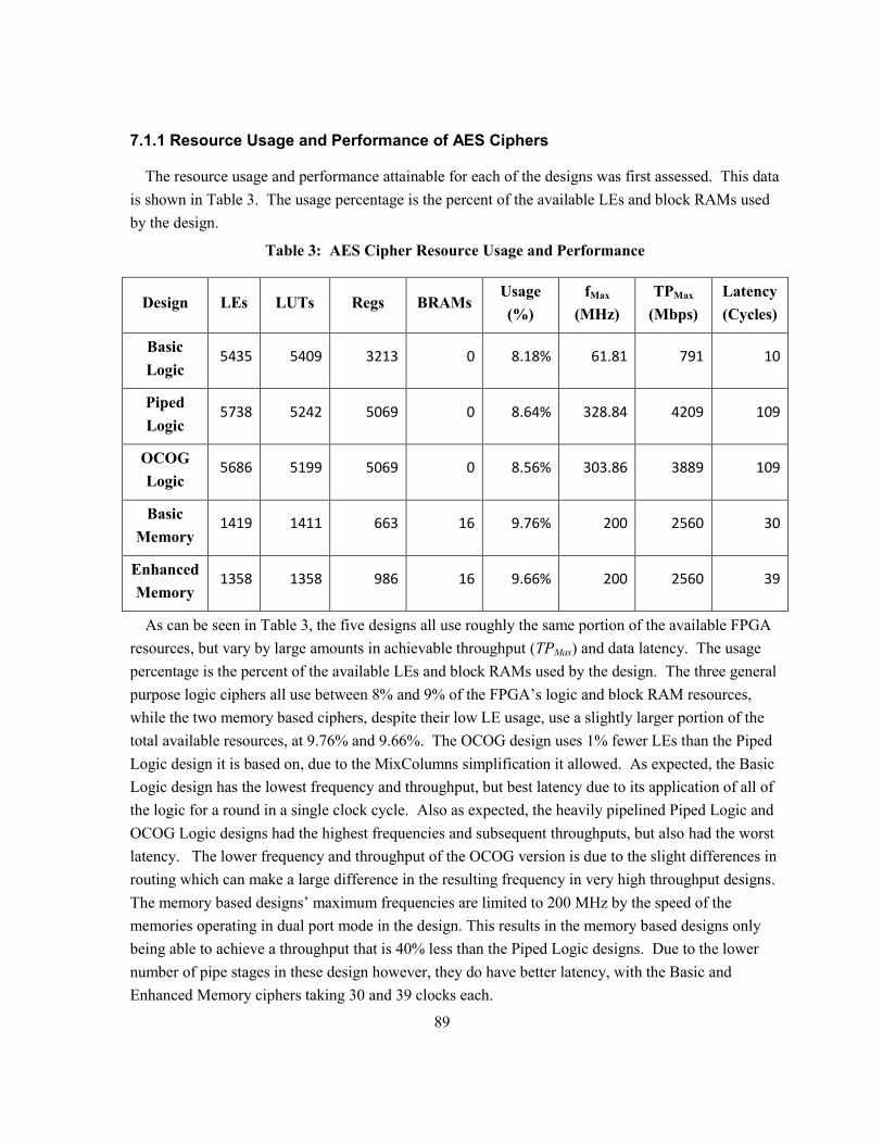
89
7.1.1 Resource Usage and Performance of AES Ciphers
The resource usage and performance attainable for each of the designs was first assessed. This data
is shown in Table 3. The usage percentage is the percent of the available LEs and block RAMs used
by the design.
Table 3: AES Cipher Resource Usage and Performance
Design LEs LUTs Regs BRAMs Usage
(%)
fMax
(MHz)
TPMax
(Mbps)
Latency
(Cycles)
Basic
Logic 5435 5409 3213 0 8.18% 61.81 791 10
Piped
Logic 5738 5242 5069 0 8.64% 328.84 4209 109
OCOG
Logic 5686 5199 5069 0 8.56% 303.86 3889 109
Basic
Memory 1419 1411 663 16 9.76% 200 2560 30
Enhanced
Memory 1358 1358 986 16 9.66% 200 2560 39
As can be seen in Table 3, the five designs all use roughly the same portion of the available FPGA
resources, but vary by large amounts in achievable throughput (TPMax) and data latency. The usage
percentage is the percent of the available LEs and block RAMs used by the design. The three general
purpose logic ciphers all use between 8% and 9% of the FPGA‟s logic and block RAM resources,
while the two memory based ciphers, despite their low LE usage, use a slightly larger portion of the
total available resources, at 9.76% and 9.66%. The OCOG design uses 1% fewer LEs than the Piped
Logic design it is based on, due to the MixColumns simplification it allowed. As expected, the Basic
Logic design has the lowest frequency and throughput, but best latency due to its application of all of
the logic for a round in a single clock cycle. Also as expected, the heavily pipelined Piped Logic and
OCOG Logic designs had the highest frequencies and subsequent throughputs, but also had the worst
latency. The lower frequency and throughput of the OCOG version is due to the slight differences in
routing which can make a large difference in the resulting frequency in very high throughput designs.
The memory based designs‟ maximum frequencies are limited to 200 MHz by the speed of the
memories operating in dual port mode in the design. This results in the memory based designs only
being able to achieve a throughput that is 40% less than the Piped Logic designs. Due to the lower
number of pipe stages in these design however, they do have better latency, with the Basic and
Enhanced Memory ciphers taking 30 and 39 clocks each.
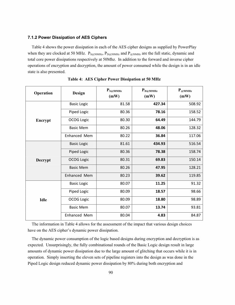
90
7.1.2 Power Dissipation of AES Ciphers
Table 4 shows the power dissipation in each of the AES cipher designs as supplied by PowerPlay
when they are clocked at 50 MHz. PS@50MHz, PD@50MHz and P@50MHz are the full static, dynamic and
total core power dissipations respectively at 50Mhz. In addition to the forward and inverse cipher
operations of encryption and decryption, the amount of power consumed while the design is in an idle
state is also presented.
Table 4: AES Cipher Power Dissipation at 50 MHz
Operation Design PS@50MHz
(mW)
PD@50MHz
(mW)
P@50MHz
(mW)
Encrypt
Basic Logic 81.58 427.34 508.92
Piped Logic 80.36 78.16 158.52
OCOG Logic 80.30 64.49 144.79
Basic Mem 80.26 48.06 128.32
Enhanced Mem 80.22 36.84 117.06
Decrypt
Basic Logic 81.61 434.93 516.54
Piped Logic 80.36 78.38 158.74
OCOG Logic 80.31 69.83 150.14
Basic Mem 80.26 47.95 128.21
Enhanced Mem 80.23 39.62 119.85
Idle
Basic Logic 80.07 11.25 91.32
Piped Logic 80.09 18.57 98.66
OCOG Logic 80.09 18.80 98.89
Basic Mem 80.07 13.74 93.81
Enhanced Mem 80.04 4.83 84.87
The information in Table 4 allows for the assessment of the impact that various design choices
have on the AES cipher‟s dynamic power dissipation.
The dynamic power consumption of the logic based designs during encryption and decryption is as
expected. Unsurprisingly, the fully combinational rounds of the Basic Logic design result in large
amounts of dynamic power dissipation due to the large amount of glitching that occurs while it is in
operation. Simply inserting the eleven sets of pipeline registers into the design as was done in the
Piped Logic design reduced dynamic power dissipation by 80% during both encryption and

91
decryption operations. The application of OCOG to all sixteen S-Boxes and four MixColumns
modules in addition to pipelining in OCOG Logic further reduced dynamic power dissipation by an
additional 17% during encryption and 10% during decryption. This is an 85% and 84%
improvement over the Basic logic design in terms of power consumption during encryption and
decryption.
The use of memory components for S-Box implementation and expanded key storage resulted in
even less dynamic power consumption during encryption and decryption than the application of
pipelining and OCOG did. The Basic Memory design reduced dynamic power dissipation by about
89% for both operations.
The Enhanced Memory design further reduces the dynamic power consumption during encryption
and decryption by an additional 23% and 17% respectively. These gains were the result of combining
the demonstratively effective strategies of using embedded block RAMs for key storage and applying
pipelining and OCOG to the 4 MixColumns modules. The use of gray code for memory encoding did
not affect the resulting design to a large degree. The enhanced memory based cipher offers the lowest
dynamic power consumption for both encryption and decryption of all of the ciphers, with a reduction
of 90% when compared to the Basic Logic cipher.
The amount of idle dynamic power consumed by the ciphers is closely related to the number of
clock enables used in the round logic. The Enhanced Memory cipher uses clock enables at every pipe
stage within its round structure, resulting in very little unneeded signal propagation when no valid
data is present. This design has the lowest idle dynamic power consumption. The Piped Logic,
OCOG Logic and Basic Memory designs all have multiple pipe stages per round, but only use one
clock enable during a single stage, allowing more unneeded signal propagation when no valid data is
present. This results in higher idle dynamic power consumption. The Basic Logic design only has
one register in its round structure, and its clock enable prevents data from propagating at all in the
design unless valid data is supplied.
7.1.3 Energy Efficiency of AES Ciphers
Table 5 shows the energy efficiencies of all of the implemented AES ciphers. Since these designs
lack a key expander, it is assumed that they will be implemented on the same chip as other logic.
This means that only the amount of static power that is proportional to the recourse utilization of the
design needs to be accounted for when energy efficiency is assessed. Each of the designs was
simulated at the maximum frequency possible without simulation errors, FMaxSim, and the power
consumption and throughput resulting at this frequency was used for determining the amount of
energy consumed per operation. TP@Max is the throughput obtained when simulating at FMaxSim.
Similarly, PS@Max and PD@Max are the static and power dissipations reported by the script when the
operation was simulated at FMaxSim,. PS prop is the amount of PS@Max that is proportional to the amount of

92
FPGA resources used by the design. The energy efficiency is assessed in terms of energy per
operation, EPerOp.
Table 5: AES Cipher Energy Efficiency
Operation Design FMaxSim
(MHz)
TP@Max
(Mbps)
PS@Max
(mW)
PS prop
(mW)
PD@Max
(mW)
EPerOp
(nJ)
Encrypt
Basic Logic 61.80 791 81.96 6.71 528.22 86.6
Piped Logic 328.73 4208 82.30 7.11 513.77 15.8
OCOG Logic 303.77 3888 81.76 7.00 391.77 13.1
Basic Mem 200.00 2560 80.98 7.90 192.05 10.0
Enhanced Mem 200.00 2560 80.83 7.81 147.51 7.8
Decrypt
Basic Logic 61.80 791 81.99 6.71 537.61 88.1
Piped Logic 328.73 4208 82.30 7.11 515.2 15.9
OCOG Logic 303.77 3888 81.80 7.00 424.21 14.2
Basic Mem 200.00 2560 80.98 7.90 191.59 10.0
Enhanced Mem 200.00 2560 80.86 7.81 158.63 8.3
As can be seen in Table 5, the amount of energy consumed per operation of each of the designs
corresponds very closely to the amount of power they dissipated at 50 MHz. The Basic Logic design,
of course, is the least efficient, while the Enhanced Memory design is the most efficient. Since only a
comparatively small amount of the total static power was considered when evaluating the energy
efficiency, it had a relatively small impact on the energy efficiency.
7.2 Energy Efficient Full AES Design
As was discussed in Chapter 5, the energy efficient Full AES design proposed was based on the
Enhanced Memory cipher design with the addition of key expansion hardware. The resulting full
AES design was capable of performing varying combinations of key expansion and cipher operations,
the power consumption and energy efficiency of which will be discussed here. As was the case for
the AES ciphers, the discussion starts with an assessment of the design‟s resource utilization and
performance, then moves on to discuss its power dissipation and energy efficiency characteristics.
The effect of varying frequency on the energy efficiency of this design is also assessed.
7.2.1 Resource Utilization and Performance of Full AES Design
As was done for the AES components, the resource usage and performance attainable for each of
the designs was first assessed. This data is shown in Table 3.
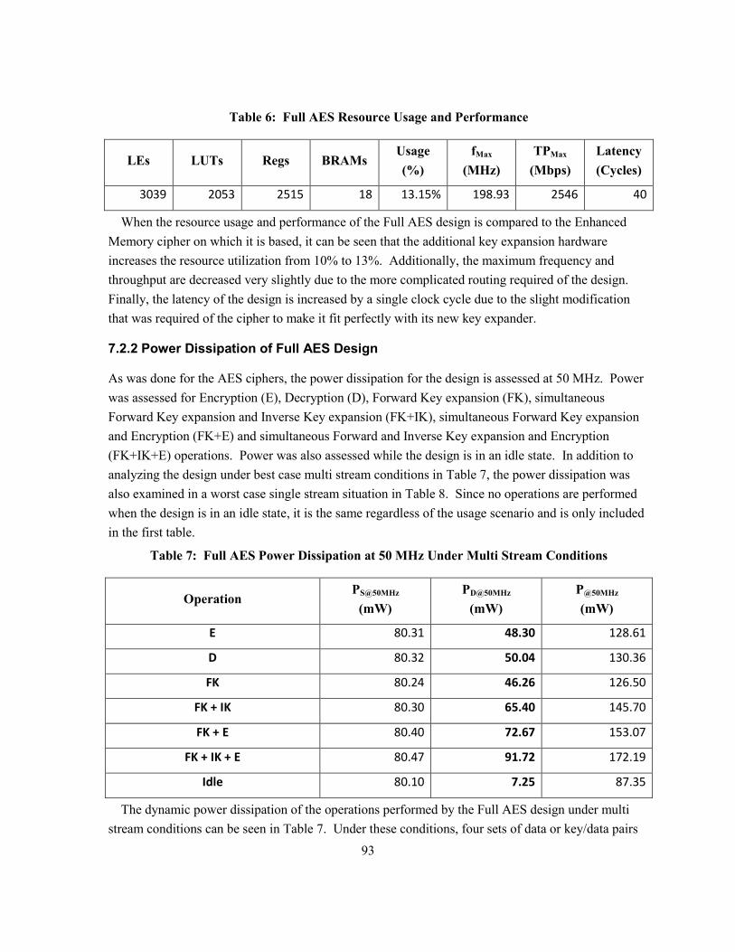
93
Table 6: Full AES Resource Usage and Performance
LEs LUTs Regs BRAMs Usage
(%)
fMax
(MHz)
TPMax
(Mbps)
Latency
(Cycles)
3039 2053 2515 18 13.15% 198.93 2546 40
When the resource usage and performance of the Full AES design is compared to the Enhanced
Memory cipher on which it is based, it can be seen that the additional key expansion hardware
increases the resource utilization from 10% to 13%. Additionally, the maximum frequency and
throughput are decreased very slightly due to the more complicated routing required of the design.
Finally, the latency of the design is increased by a single clock cycle due to the slight modification
that was required of the cipher to make it fit perfectly with its new key expander.
7.2.2 Power Dissipation of Full AES Design
As was done for the AES ciphers, the power dissipation for the design is assessed at 50 MHz. Power
was assessed for Encryption (E), Decryption (D), Forward Key expansion (FK), simultaneous
Forward Key expansion and Inverse Key expansion (FK+IK), simultaneous Forward Key expansion
and Encryption (FK+E) and simultaneous Forward and Inverse Key expansion and Encryption
(FK+IK+E) operations. Power was also assessed while the design is in an idle state. In addition to
analyzing the design under best case multi stream conditions in Table 7, the power dissipation was
also examined in a worst case single stream situation in Table 8. Since no operations are performed
when the design is in an idle state, it is the same regardless of the usage scenario and is only included
in the first table.
Table 7: Full AES Power Dissipation at 50 MHz Under Multi Stream Conditions
Operation PS@50MHz
(mW)
PD@50MHz
(mW)
P@50MHz
(mW)
E 80.31 48.30 128.61
D 80.32 50.04 130.36
FK 80.24 46.26 126.50
FK + IK 80.30 65.40 145.70
FK + E 80.40 72.67 153.07
FK + IK + E 80.47 91.72 172.19
Idle 80.10 7.25 87.35
The dynamic power dissipation of the operations performed by the Full AES design under multi
stream conditions can be seen in Table 7. Under these conditions, four sets of data or key/data pairs
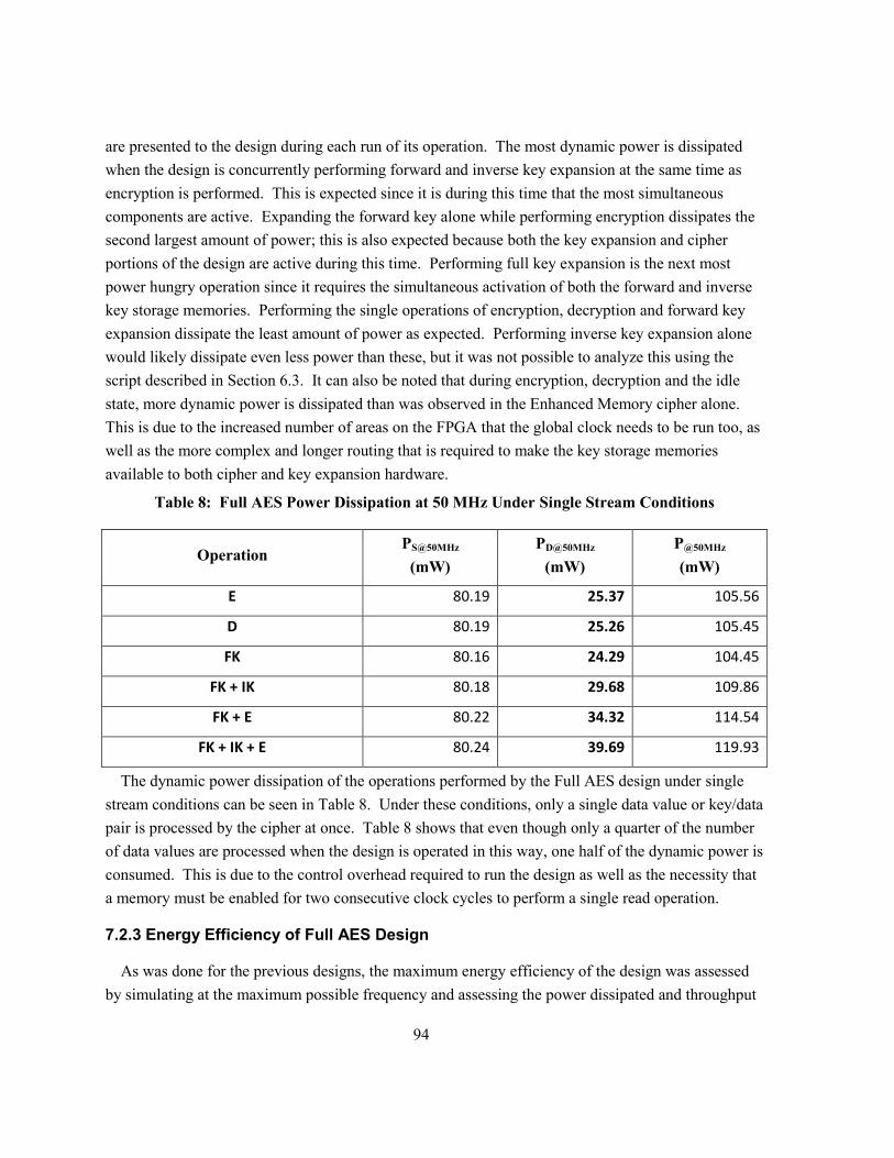
94
are presented to the design during each run of its operation. The most dynamic power is dissipated
when the design is concurrently performing forward and inverse key expansion at the same time as
encryption is performed. This is expected since it is during this time that the most simultaneous
components are active. Expanding the forward key alone while performing encryption dissipates the
second largest amount of power; this is also expected because both the key expansion and cipher
portions of the design are active during this time. Performing full key expansion is the next most
power hungry operation since it requires the simultaneous activation of both the forward and inverse
key storage memories. Performing the single operations of encryption, decryption and forward key
expansion dissipate the least amount of power as expected. Performing inverse key expansion alone
would likely dissipate even less power than these, but it was not possible to analyze this using the
script described in Section 6.3. It can also be noted that during encryption, decryption and the idle
state, more dynamic power is dissipated than was observed in the Enhanced Memory cipher alone.
This is due to the increased number of areas on the FPGA that the global clock needs to be run too, as
well as the more complex and longer routing that is required to make the key storage memories
available to both cipher and key expansion hardware.
Table 8: Full AES Power Dissipation at 50 MHz Under Single Stream Conditions
Operation PS@50MHz
(mW)
PD@50MHz
(mW)
P@50MHz
(mW)
E 80.19 25.37 105.56
D 80.19 25.26 105.45
FK 80.16 24.29 104.45
FK + IK 80.18 29.68 109.86
FK + E 80.22 34.32 114.54
FK + IK + E 80.24 39.69 119.93
The dynamic power dissipation of the operations performed by the Full AES design under single
stream conditions can be seen in Table 8. Under these conditions, only a single data value or key/data
pair is processed by the cipher at once. Table 8 shows that even though only a quarter of the number
of data values are processed when the design is operated in this way, one half of the dynamic power is
consumed. This is due to the control overhead required to run the design as well as the necessity that
a memory must be enabled for two consecutive clock cycles to perform a single read operation.
7.2.3 Energy Efficiency of Full AES Design
As was done for the previous designs, the maximum energy efficiency of the design was assessed
by simulating at the maximum possible frequency and assessing the power dissipated and throughput

95
attainable. In addition to assessing the efficiency in a multi stream situation in Table 9, the design‟s
energy efficiency under the worst case single stream operating conditions was also examined in Table
10. Since this is a complete design, it is reasonable to assume that it could be implemented on its
own in an FPGA in addition to being implemented as part of a larger SoC. In this situation, the
energy efficiency of the design must take the entire static power dissipation of the FPGA into
consideration. Table 11 is used to show this under the multi stream operation condition.
Table 9: Full AES Energy Efficiency Under Multi Stream Conditions
Operation FMaxSim
(MHz)
TP@Max
(Mbps)
PS@MaxSim
(mW)
PS prop
(mW)
PD@MaxSim
(mW)
EPerOp
(nJ)
E 198.89 2546 81.03 10.65 192.34 10.2
D 198.89 2546 81.05 10.65 199.28 10.6
FK 198.89 2546 80.73 10.61 184.16 9.8
FK + IK 198.89 2546 81 10.65 260.28 13.6
FK + E 198.89 2546 81.39 10.70 289.23 15.1
FK + IK + E 198.89 2546 81.66 10.74 364.99 18.9
Table 10: Full AES Energy Efficiency Under Single Stream Conditions
Operation FMaxSim
(MHz)
TP@Max
(Mbps)
PS@MaxSim
(mW)
PS prop
(mW)
PD@MaxSim
(mW)
EPerOp
(nJ)
E 198.89 636 80.51 0.00 101.11 20.5
D 198.89 636 80.51 0.00 100.72 22.4
FK 198.89 636 80.42 10.57 96.74 21.6
FK + IK 198.89 636 80.49 10.58 118.21 25.9
FK + E 198.89 636 80.64 10.60 136.93 29.7
FK + IK + E 198.89 636 80.71 10.61 158.3 34.0
When comparing the energy efficiency values in Table 9 and Table 10 it can be seen that the
energy efficiency of the design is basically cut in half when it is operated in single stream mode.
Even though half the dynamic power is consumed by the design when operating in this way, its
efficiency is reduced due to the four times drop in throughput.

96
Table 11 shows the effect including static power in the determination of energy efficiency. The
first column shows the amount of energy consumed per operation if static power is completely
disregarded. This value is useful for comparison purposes but is only an approximation of energy per
operation. The second column shows the familiar value of energy consumed per operation assuming
that the design will be part of a larger design that takes up a significant portion of the remaining
FPGA resources. This value is useful if the Full AES design is intended for use in a system on chip.
Finally, the third column shows the amount of energy consumed per operation if the full amount of
static power dissipated by the FPGA is considered. This value is a valid measure of energy efficiency
if the Full AES design is intended to be used by its self on an FPGA. It should be noted that the
reason the medium sized EP2C35 FPGA used would be required for this in order to accommodate all
of the input and output pins required by an AES design.
Table 11: Effect of Considering Static Power on Energy Efficiency
Operation Dynamic EPerOp
(nJ)
Prop Static EPerOp
(nJ)
Full EPerOp
(nJ)
E 9.7 10.2 13.7
D 10.0 10.6 14.1
FK 9.3 9.8 13.3
FK + IK 13.1 13.6 17.2
FK + E 14.5 15.1 18.6
FK + IK + E 18.4 18.9 22.5
The impact of disregarding the static component of power dissipation when assessing the energy
efficiency of the Full AES design can be seen in Table 11. If the design was to be implemented in a
larger system on chip, disregarding the static power of the FPGA would result in energy efficiency
estimates that were 3% to 5% overly optimistic. If the design was to be implemented by itself on an
FPGA however, disregarding the static power dissipation would have a much larger impact, resulting
in energy efficiency estimates that are 20% to 55% overly optimistic. As such, it is important to take
static power into consideration if a design is intended to be implemented on its own in an FPGA or
takes up a significant portion of the FPGA‟s resources.
7.2.4 Effect of Varying Frequency on Energy Efficiency
Finally, the effects of varying the frequency the Full AES design is run at were assessed. Figure 52
shows the amount of energy consumed per encryption when the design was simulated at every
frequency from its maximum of just under 200 MHz down to 10 MHz in 10 MHz increments.

97
Figure 52: Effect of Varying Frequency on Energy Efficiency
Energy efficiency disregarding static power dissipation, using proportional static power dissipation,
and full static power dissipation are shown in Figure 52. The lowest line shows that, as expected,
there is no change in energy consumed per encryption if static power dissipation is completely
disregarded. The middle curve shows that if only a static power dissipation which is proportional to
the amount of FPGA resources used is considered, reduction in frequency will decrease the energy
efficiency of the design, but it will only do so at an appreciable amount at very low speeds. The
upper curve shows that if the full static power dissipation of the FPGA is considered reducing the
operating frequency could have a large impact on the energy efficiency of the design. As can be seen
in the diagram, reducing the clock speed to less than 80 MHz would cut the energy efficiency of the
design in half.
7.3 Comparison to Previous Research
Comparison of the Full AES design implemented in this thesis to other works is difficult, mostly due
to the lack of research that has been in the area of energy efficient FPGA based AES
implementations. Though there have been many excellent FPGA based AES implementations, nearly
all of them focus on high throughput or low resource utilization, and do not evaluate the power
dissipated by the design let alone its energy efficiency. Though they were intended for lower power
consumption as opposed to high energy efficiency and only give values dynamic power consumption,
the designs discussed in Section 3.4 were evaluated for energy efficiency for comparison with the
energy efficient Full AES implementation described in 5.5.
The two main factors which must be considered comparing designs for energy efficiency are the
technology that the design was implemented on and the reliability of the power estimates that were
98
obtained. The platform in which the designs were implemented can have a large impact on their
perceived energy efficiencies. Different FPGAs implement general purpose logic and embedded
functional blocks such as memories differently, and have slightly different routing networks. As
such, implementing the same design on different hardware platforms results in different resource
utilizations, maximum frequencies and power dissipations. In order to have a fairer comparison,
these metrics must be normalized. The second thing that must be considered when comparing
designs is the reliability of the power consumption estimates that are available. Of course, the most
reliable method for determining core power dissipation on a device would be to physically measure it
while it is in operation. This practice is difficult and time consuming to set up so it is rarely done in
practice. The second most reliable method for assessing power dissipation is to use vendor supplied
power estimation tools such as XPower or PowerPlay, and provide it with signal activity information
based on accurate simulation data. The least reliable method is by using power estimator websites or
spreadsheets which estimate power consumption based on design utilization and sometimes routing
information that is based solely on synthesis reports or hardware utilization. These designs use
default or user entered signal activity estimates instead of activity rates based on a simulation of the
design‟s intended operation.
7.3.1 Resource Utilization and Performance of Compared AES Designs
Table 12 shows a resource usage and performance comparison between the discussed designs. The
resource usage of each device is normalized to the Cyclone II used in this thesis by showing it as a
percentage of the available equivalent EP2C35 resources. Since registers and LUTs are occasionally
placed by themselves in a LE during Cyclone II fitting, it is impossible to tell exactly how many LEs
would be actually used by the comparison designs when implemented on the EP2C35. Because of
this, the best case, though unlikely, situation of having all registers fit into LEs where the LUT is
already used is assumed when determining the normalized usage percentage. Even though the Virtex
II and Virtex 4 are more advanced devices than the Cyclone II and are more capable of achieving
high clock speeds, the obtained maximum frequency was not normalized.
As can be seen in Table 12, the proposed Full AES design uses the largest amount of resources of
any of the compared designs, though the functionality of the designs must also be considered when
assessing the significance of this. The proposed Full AES design offers full encryption and
decryption operations along with the option of performing full key expansion in parallel with
encryption.
The two proposed designs by Katashita et al [31], BRAM-I and LUT-II, do not include any key
expansion hardware and must be operated using a pre expanded key, limiting their functionality. If a
key expander were also included, it would have increased the amount of resources consumed.
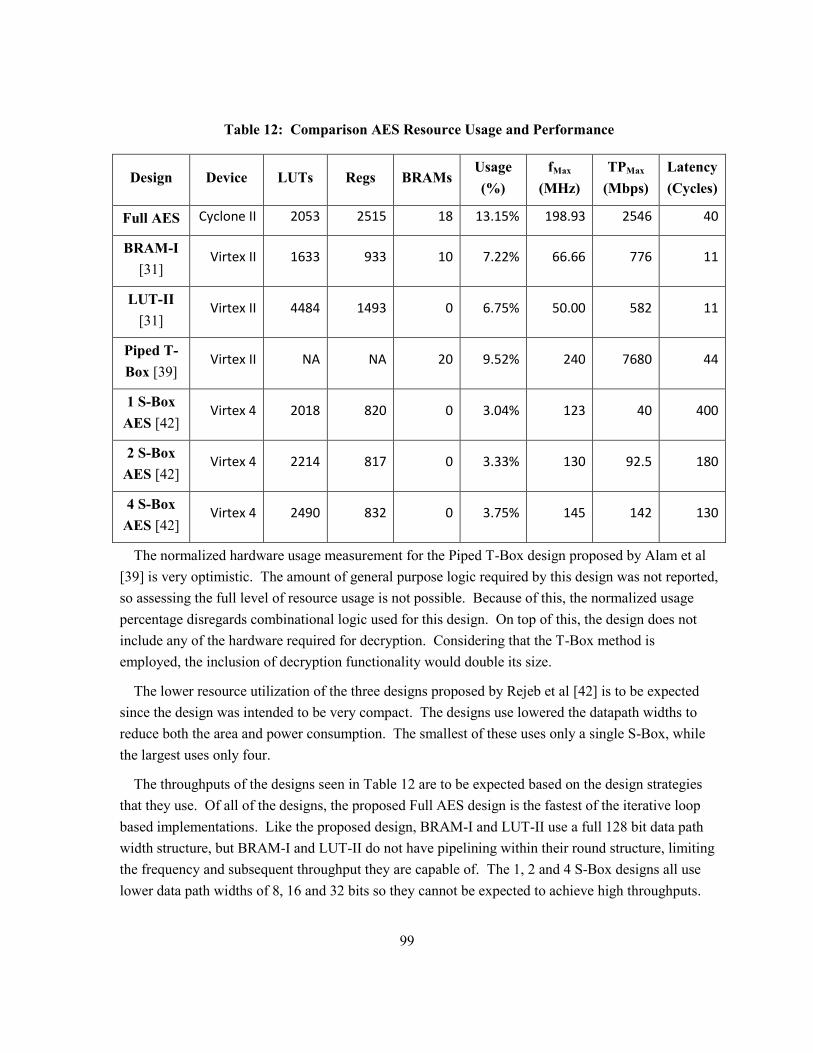
99
Table 12: Comparison AES Resource Usage and Performance
Design Device LUTs Regs BRAMs Usage
(%)
fMax
(MHz)
TPMax
(Mbps)
Latency
(Cycles)
Full AES Cyclone II 2053 2515 18 13.15% 198.93 2546 40
BRAM-I
[31] Virtex II 1633 933 10 7.22% 66.66 776 11
LUT-II
[31] Virtex II 4484 1493 0 6.75% 50.00 582 11
Piped T-
Box [39] Virtex II NA NA 20 9.52% 240 7680 44
1 S-Box
AES [42] Virtex 4 2018 820 0 3.04% 123 40 400
2 S-Box
AES [42] Virtex 4 2214 817 0 3.33% 130 92.5 180
4 S-Box
AES [42] Virtex 4 2490 832 0 3.75% 145 142 130
The normalized hardware usage measurement for the Piped T-Box design proposed by Alam et al
[39] is very optimistic. The amount of general purpose logic required by this design was not reported,
so assessing the full level of resource usage is not possible. Because of this, the normalized usage
percentage disregards combinational logic used for this design. On top of this, the design does not
include any of the hardware required for decryption. Considering that the T-Box method is
employed, the inclusion of decryption functionality would double its size.
The lower resource utilization of the three designs proposed by Rejeb et al [42] is to be expected
since the design was intended to be very compact. The designs use lowered the datapath widths to
reduce both the area and power consumption. The smallest of these uses only a single S-Box, while
the largest uses only four.
The throughputs of the designs seen in Table 12 are to be expected based on the design strategies
that they use. Of all of the designs, the proposed Full AES design is the fastest of the iterative loop
based implementations. Like the proposed design, BRAM-I and LUT-II use a full 128 bit data path
width structure, but BRAM-I and LUT-II do not have pipelining within their round structure, limiting
the frequency and subsequent throughput they are capable of. The 1, 2 and 4 S-Box designs all use
lower data path widths of 8, 16 and 32 bits so they cannot be expected to achieve high throughputs.

100
Finally though the Piped T-Box design also uses a 32 bit data path width, it has the highest
throughput of the designs due to the fact that it also features a fully unrolled round loop structure.
7.3.2 Energy Efficiency of Compared AES Designs
Table 13 shows an energy efficiency comparison between the discussed designs. As was done in
previous sections, the energy efficiency is determined based on the amount of core energy consumed
per operation with only the fraction of static power which is proportional to the resource utilization
considered. For the purposes of this comparison, a normalized total static power of 80 mW is
assumed, and the dynamic power dissipation is normalized using a scaling factor based on the
original FPGA used. In order to find the proper scaling factors for each device, power estimator
spreadsheets and websites [24] [23] [43] were used to determine the dynamic power dissipation on all
three devices when a specific amount of general purpose logic and block RAM resources were used
with the same operating frequency and activity factors. It was found that the Virtex II and Virtex 4
FPGAs dissipate 4.5 and 1.1 times more dynamic power than the Cyclone II with identical resource
usage and operating conditions. The amount of energy consumed per operation for each design was
calculated assuming that the design was run at its maximum frequency.
The results in Table 13 show that the proposed Full AES design is the most energy efficient of all
the compared designs.
Examining the amount of energy consumed per operation in BRAM-I and LUT-II proposed by
Katashita [31] gives further insight into some of the observations that were made during the analysis
of the candidate AES ciphers of this thesis. These designs add glitch reducing elements to ciphers
which use block RAM and general purpose logic based S-Boxes in BRAM-I and LUT-II respectively.
Similar to what was seen in Section 7.1, the use of block RAMs resulted in BRAM-I consuming less
energy per operation than LUT-II. The improvements in energy efficiency in the Full AES design
over BRAM-I are due to the large increases in throughput and glitch reduction resulting from
additional pipelining, as well the reduced power consumption due to the use of OCOG.
Even though the use of block RAMs is generally more energy efficient then the use of general
purpose logic, the Piped T-Box design proposed by Alam [39] was likely less energy efficient than
the proposed Full AES design due to its over reliance on them. Since FPGAs only have block
memory resources arranged in a fixed structure throughout the FPGA if a large portion of them are
used by a design, routing will be required across the entire chip, increasing dynamic power
consumption. The larger size of block RAMs required to implement T-Boxes are also likely to
dissipate more power than the smaller ones which can be used to fit S-Boxes in them.

101
Table 13: Comparison AES Normalized Energy Efficiency
Operation Design FAssed At
(MHz)
TP@Assd
(Mbps)
PSNorm
(mW)
PS prop
(mW)
PDNorm
(mW)
EProp
(nJ)
Encrypt
Full AES 198.89 2546 81.03 10.65 192.34 10.2
BRAM-I
[31] 66.66 776 80 5.78 69 12
LUT-II
[31] 50.00 582 80 5.40 68 16
Piped T-
Box [39] 240 7680 80 7.62 821 14
Decrypt
Full AES 198.89 2546 81.05 10.65 199.28 10.6
BRAM-I
[31] 66.66 776 80 5.78 73.88 13
LUT-II
[31] 50.00 582 80 5.40 70.93 17
Not
Specified
1 S-Box
AES [42] 123 40 80 2.43 125 406
2 S-Box
AES [42] 130 92.5 80 2.67 139 196
4 S-Box
AES [42] 145 142 80 3.00 154 141
There are several likely reasons why the low data path width designs by Reheb [42] appear to have
performed so poorly in terms of energy efficiency. Since the designs have such low throughputs, it is
very hard for them to offset the power that they dissipate. With such small data path widths of 8, 16
and 32 bits in 1 S-Box AES, 2 S-Box AES and 4 S-box AES, the designs are likely to be bogged
down with a lot of extra overhead for the implementation of control logic. This will slow them down
and cause additional power consumption. Additionally, since MixColumns operations require 32 bits
of input data, designs that have a lower data path width than this will spend a lot of extra time with
MixColumns waiting for enough data to be available for it, hurting both power consumption and
throughput. The designs do disable hardware when it cannot operate which lessens the impact on

102
dynamic power consumption, but there is nothing that can be done to improve the very low
throughput. Additionally, the amounts of power consumption originally specified are likely not as
reliable as they could be since the power usages of the designs were estimated using a power
estimator spreadsheet instead of using actual switching rates from simulations. It is likely that the
signal activity estimates did not take into consideration the large amount of time that most of the
components will spend in an inactive state, resulting in overly pessimistic predictions of dynamic
power consumption.
Considering the differences in functionality of the designs, the energy efficiency of the proposed
Full AES design seems even more impressive. The Full AES design offers the option of full or
partial key expansion on the fly, and allows for an independent key to be stored for each data stream.
The BRAM-I and LUT-II designs are not able to perform key expansion, and the Piped T-Box design
forces a single key to be used for all encryptions until a key change takes place. The key must be pre
expanded before encryption can take place, which will significantly slow down the operation of the
cipher if frequent key changes are necessary. Additionally, the Piped T-Box design does not support
decryption.
7.4 Discussion and Analysis
The purpose of this section is to provide and analysis and more detailed discussion on some of the
observations made during the reporting of results.
7.4.1 The AES Energy Analyzer
The AES Energy Analyzer scripting tool played a large role in the analysis of the FPGA energy
efficiency strategies in AES as well as the evaluation of the final energy efficient design. In addition
to managing the complex compilation flow used, the script was able to fully automate the simulation
and power analysis processes required to assess the energy efficiency for each of the commonly
required AES operations. The script allowed the full AES design to have its power and energy
consumption profile fully characterized. In addition to allowing for the evaluation of the design
under both best and worst case data stream utilization conditions, it also allowed for power
dissipation while in an idle state to be assessed. Finally, the script allowed for easy assessment of the
design at multiple operating frequencies. In short, the AES Energy Analyzer allowed for a much
more in depth and complete power and energy analysis to be performed on the proposed FPGA
design strategies and full energy efficient AES implementation than has been possible in previous
research.

103
7.4.2 Energy Efficiency Strategies in AES
The results presented in Section 7.1 show the effectiveness of the use of pipelining, OCOG and
embedded block RAM components in reducing dynamic power consumption and increasing energy
efficiency in AES.
The use of block RAMs appears to have had the largest impact on power consumption and energy
efficiency in AES, reducing dynamic power and energy per operation by up to nearly 90%. It should
be noted however, that using the synchronous block RAMs meant that the round logic was effectively
broken up into three pipe stages, reducing power through pipelining in addition to simply using
embedded resources. That said, considering the large amount of power savings obtained using
effectively three pipe stages and block RAMs when compared to slightly lesser power savings from
the use of eleven pipe stages in the heavy pipelining design, it is apparent that the use of block RAM
components does have a significant impact on power consumption and energy efficiency in AES.
The use of heavy pipelining had a large impact on power consumption and energy efficiency in
AES as well, reducing dynamic power and energy per operation by about 80%. This technique
improved dynamic power consumption through glitch reduction and improved throughput by
increasing the maximum possible frequency. Unfortunately, increasing the maximum throughput
through the increased frequency afforded by pipelining doesn‟t have a large impact on energy
efficiency due to the fact that increasing the operating frequency of a design will increase its dynamic
power consumption at the same rate as it increases its throughput (recall equation (29)). Though
increasing the throughput in this way cannot offset dynamic energy consumption, it can offset the
potentially large static power consumption of an FPGA for greater energy efficiency, as was
illustrated in Figure 52. The effect of increasing throughput by increasing frequency has a larger
impact on energy efficiency of designs implemented on their own in a FPGA as opposed to designs
assumed to be implemented as part of a larger SoC. Regardless of the implementation, it was shown
that the use of pipelining has large benefits to the energy efficiency of AES through dynamic power
reduction.
The use of Opportunistic Combinational Operand Gating had a positive impact on power and
energy usage in AES, with the combination of OCOG and heavy pipelining reducing dynamic power
dissipation and energy per operation of by 85% and 84% for encryption and decryption respectively.
This is a reduction of an additional 17% and 10% for encryption and decryption when compared to
the dynamic power dissipation and energy per operation possible through heavy pipelining alone.
The technique allowed for the reduction of dynamic power in AES by gating out specific LUTs that
are not required by the current operation, and reducing the amount of hardware required by the
design. It did not cause any additional logic usage since it simply inserts the gating signal into the
unused inputs of LUTs that were not fully utilized. In fact, it allowed for the simplification of the
MixColumns module used, reducing the number of Logic Elements required by the design by 1%

104
when compared to the heavily pipelined design on which it is based. The large reduction in power
can also be partially attributed to this simplified logic and subsequent simplified routing it allows.
Unfortunately, The technique did reduce the maximum frequency and subsequent throughput possible
when compared to the heavily pipelined design. This was likely due to the slightly increased routing
required to account for the additional gating signals. Fortunately, as was mentioned previously,
reduction in throughput due to lower operating frequency does not have a significant impact on
energy efficiency in most situations.
7.4.3 The Full Energy Efficient AES Implementation
The full energy efficiency AES implementation proposed was fully characterized using the AES
Energy Analyzer and was found to be more energy efficient than any of the compared designs which
included power estimation data. The largest reason for this efficiency was the successful combination
of the energy efficiency strategies introduced in Chapter 4 . In addition to the cipher design strategies
evaluated in Section 7.4.2, the use of economic key expansion also improved the energy efficiency of
the design. This strategy made sure that the design never had to unnecessarily perform key expansion
operations while ensuring the design could be used on independent streams of data, maximizing its
usefulness.
Through the use of the AES Energy Analyzer, it was found that the design was most energy
efficient when it was fully utilized and running at its maximum frequency. Though a dynamic power
reduction of 50% was shown to be possible by running only one data stream though the design at
once instead of four, it was found that energy efficiency was reduced by nearly 50% as well. This
illustrates that more than just the dynamic power consumption of a design must be considered when
assessing energy efficiency. Reducing the frequency that the design is run at can also have a large
impact on its energy efficiency depending on whether the design is implemented as part of a larger
SoC or on its own. If the design was implemented on its own, a reduction in frequency of only 60%
could reduce its energy efficiency by 50%. These results indicate that care must be taken if frequency
scaling is used to reduce to power consumption of the Full AES design implemented on its own if
energy efficiency is of any consequence.
7.5 Chapter Summary
Over the course of this chapter, many observations were made about the energy efficient Full AES
design, and its dynamic power reduction techniques. The most important of these are summarized
here.
The Full AES design proposed was seen to be very energy efficient when compared to current
FPGA based AES designs which have had their power dissipation rates assessed. The energy
efficiency of its cipher is obtained through the use of synchronous block RAMs for S-Box
implementation and expanded key storage as well as heavy pipelining and the application of

105
Opportunistic Combinational Operand Gating. The energy efficiency of the design is further
enhanced by its flexible key expander which allows for the minimum amount of expander energy
usage possible while ensuring the cipher‟s usefulness regardless of its application.
The effectiveness of the energy efficiency techniques was assessed by applying them to a simple
iterative combinational logic based cipher. When examining the cipher alone, the use of embedded
block RAMs was able to reduce the dynamic power consumption of a basic combinational logic
cipher by 90%. Alternately, the application of heavy pipelining on the basic combination logic cipher
improved dynamic power consumption by 80%. When Opportunistic Combinational Operand Gating
was applied to the heavy pipelined version of cipher, 17% and 10% reductions in dynamic power
consumptions were observed during encryption and decryption respectively.
The energy efficiency of the Full AES design was also examined under less than ideal conditions.
It was found that energy efficiency would be cut in half if the design were operated under the worse
case condition that only one value could be processed at a time. Additionally, if the design is
implemented on its own in an FPGA, energy efficiency can be reduced significantly if it is not run at
is maximum operating frequency.

106
Chapter 8
Conclusions
8.1 Summary and Contributions
In this thesis, the development and assessment of a high energy efficiency FPGA based full AES
implementation was discussed. The proposed design takes advantage of pipelining, the use of
embedded block RAM components, register clock enable signals, Opportunistic Combinational
Operand Gating, and flexible economic key expansion functionality to keep the amount of energy
consumed per operation to as low a level as possible. An assessment of the impact of the energy
efficiency design strategies of pipelining, the use of embedded block RAMs and Opportunistic
Combinational Operand Gating was made. The power and energy profile for the proposed design
was fully characterized in all usage situations allowing recommendations to be made for the
conditions it should be run under for the best possible energy efficiency.
The three main contributions of this work include the first known attempt at the implementation of
an energy efficient FPGA based AES design, the most thorough and complete assessment of the
power and energy consumption of an FPGA based AES design, and the introduction of a novel FPGA
dynamic power consumption strategy called Opportunistic Combinational Operand Gating. The
effort in implementing energy efficiency strategies yielded a design that was found to have better
energy efficiency than all of the other examined FPGA based AES designs that included a power
analysis. On top of this, it also offered greater functionality in its ability to handle multiple
simultaneous encryption sessions. The in depth analysis of the design in terms of power and energy
consumption was enabled by use of the AES Energy Analyzer scripting tool which automated the
assessment process and provided detailed results. Finally, the Opportunistic Combinational Operand
Gating technique proposed demonstrated the ability to lower dynamic power consumption at no
additional hardware cost.
8.2 Future Work
The research performed in this thesis also exposed several new research areas that could be explored.
The first of these is the potential to make further improvements to the energy efficient full AES
design. Though the use of a composite field GF(((22)
2)
2 based multiplicative inversion in the S-Boxes
was examined, it has been suggested that GF((24)
2) based implementations could dissipate less power
[44] [42]. A Pipelined version of this form of S-Box with Opportunistic Combinational Operand
Gating applied could lead to efficient results. Also, it would be valuable to experiment with other
AES structures, such as using lower data path widths or fully unrolling the loop architecture in order
to evaluate the impact of these design decisions on energy efficiency. Experimenting with enabling

107
data to be input over multiple clock cycles to reduce the number of input pins required would also be
useful.
Though the AES Energy Efficiency Analyzer performed its function very well, it could be
improved upon. The most notable way would be to generalize the tool so it could be used for a
variety of different design types instead of just AES. There are many non-AES FPGA based designs
that could benefit from the in depth power and energy analysis provided by the script. Additionally,
generalizing the tool to work with other FPGA manufacturers would make it much more useful. As
the design is implemented currently, it only works for Altera based designs due mostly to the method
used to generate test benches for simulation. One of the largest problems in comparing the proposed
design to other works was how to compare designs implemented on different hardware platforms.
This problem could be alleviated if the script was also able to assess designs implemented on Xilinx
hardware. The script could also be expanded to supply even more information which would be
useful for power and energy analysis such as I/O power estimates or the number of times important
signals transition during simulation. Being able to track the number of times a signal transitions
would aid greatly in evaluating the impact of power reduction techniques, while having I/O power
data would be beneficial for evaluating non SoC designs.
Finally, the results obtained through the use of Opportunistic Combinational Operand Gating
appear to be promising, but further study is required to determine if it really is an effective FPGA
power reduction strategy. Though the results observed in pipelined AES were very promising it is
difficult to tell if the results are purely because of OCOG or are also the result of other design,
compilation, or device technology factors. Implementing the strategy on a variety of different designs
of varying sizes, complexities and structures would help to further explore its capabilities.
Additionally, experimenting with different device technologies and compilation tools would also help
evaluate its effectiveness. Currently, the strategy is rather cumbersome to implement manually, so
software tools that could automate the process would be very helpful during further testing.

108
Appendix A
Glossary of Acronyms
AES Advanced Encryption Standard
AED AES Energy Data
AEP AES Energy Project
ASIC Application Specific Integrated Circuit
CBC Cipher Block Chaining
CSV Comma Separated Value
DES Data Encryption Standard
DSP Digital Signal Processor
ECB Electronic Code Book
EDA Electronic Design Automation
FPGA Field Programmable Gate Array
FSM Finite State Machine
HDL Hardware Description Language
LAB Logic Array Block
LUT Look Up Table
LE Logic Element
LSDW Least Significant Double Word
LSW Least Significant Word
MSB Most Significant Bytes
MSDW Most Significant Double Word
NIST National Institute of Standard and Technology
OCOG Opportunistic Combinational Operand Gating
PLL Phase Locked Loop
RAM Random Access Memory
ROM Read Only Memory

109
RTL Register Transfer Level
SAF Signal Activity File
SoC System on Chip
VCD Value Change Dump
VHDL Very high speed integrated circuit (VHSIC) Hardware Description Language

110
Bibliography
[1] IBM Corp. (2008). IBM 4764 product and PCIXCC feature overview [Online]. Available:
http://www-03.ibm.com/security/cryptocards/pcixcc/overview.shtml
[2] NXP Corp. (2008). NXP takes lead on security for contactless smart cards [Online]. Available:
http://www.nxp.com/news/content/file_1273.html
[3] Altera Corp. (2008, November). Stratix IV device handbook [Online]. Available:
http://www.altera.com/literature/hb/stratix-iv/stratix4_handbook.pdf
[4] Altera Corp. (2008, November). Quartus II development software literature: PowerPlay power
analysis [Online]. Available: http://www.altera.com/literature/hb/qts/qts_qii5v3_03.pdf
[5] P. Hämäläinen, M. Hännikäinen and T. Hämäläinen, "Review of Hardware Architectures for
Advanced Encryption Standard Implementations Considering Wireless Sensor Networks," Embedded
Computer Systems: Architectures, Modeling, and Simulation, pp. 443-453, 2007.
[6] D. Raths. (2006, December 19). Energy hogs on the server farm [Online]. Available:
http://www.govtech.com/pcio/102970?id=102970&full=1&story_pg=1
[7] FIPS Publication 197, "the Advanced Encryption Standard (AES)," U.S. DoC/NIST, November,
2001.
[8] J. Daemen and V. Rijmen, Design of Rijndael : AES--the Advanced Encryption Standard. Berlin ;
New York: Springer, 2002, pp. xvii, 238 p.
[9] W. Stallings and Stallings,William.Network and internetwork security, Cryptography and
Network Security : Principles and Practice. ,4th ed ed.Upper Saddle River, N.J.: Pearson/Prentice
Hall, 2006, pp. xvi, 680 p.
[10] A. J. Menezes, P. C. Van Oorschot and S. A. Vanstone, Handbook of Applied Cryptography.
Boca Raton: CRC Press, 1997, pp. xxviii, 780 p.
[11] A. Rudra, P. K. Dubey, C. S. Jutla, V. Kumar, J. R. Rao and P. Rohatgi, "Efficient rijndael
encryption implementation with composite field arithmetic," in CHES '01: Proceedings of the Third
International Workshop on Cryptographic Hardware and Embedded Systems, 2001, pp. 171-184.
[12] A. Satoh, S. Morioka, K. Takano and S. Munetoh, "A compact rijndael hardware architecture
with S-box optimization," in ASIACRYPT '01: Proceedings of the 7th International Conference on the
Theory and Application of Cryptology and Information Security, 2001, pp. 239-254.

111
[13] X. Zhang and K. K. Parhi, "High-speed VLSI architectures for the AES algorithm," IEEE
Transactions on very Large Scale Integration (VLSI) Systems, vol. 12, pp. 957-967, 09. 2004.
[14] J. Zhang, Q. Zuo and T. Zhang, "Reducing the power consumption of the AES S-box by SSC,"
in 2007 International Conference on Wireless Communications, Networking and Mobile Computing,
WiCOM 2007, Startdate 20070921-Enddate 20070925, 2007, pp. 2226-2229.
[15] E. Mui, "Practical Implementation of Rijndael S-Box Using Combinational Logic," 2007.
[16] M. Feldhofer, K. Lemke, E. Oswald, F. Standaert, T. Wollinger and J. Wolkerstorfer, "State of
the Art in Hardware Architectures," Information Society Technologies, September 2005.
[17] Altera Corp. (2007, February). Cyclone II device family data sheet [Online]. Available:
http://www.altera.com/literature/hb/cyc2/cyc2_cii51001.pdf
[18] Xilinx Corp. (2007, November). Virtex-II platform FPGAs: Complete data sheet [Online].
Available: http://www.xilinx.com/support/documentation/data_sheets/ds031.pdf
[19] Altera Corp. (2007, November). FPGA power management and modeling techniques [Online].
Available: http://www.altera.com/literature/wp/wp-01044.pdf
[20] J. Lamoureux and W. Luk, "An Overview of Low-Power Techniques for Field-Programmable
Gate Arrays," Adaptive Hardware and Systems, 2008. AHS '08. NASA/ESA Conference on, pp. 338-
345, 2008.
[21] Altera Corp. (2008, November). Quartus II development software literature: Power optimization
[Online]. Available: http://www.altera.com/literature/hb/stratix-iv/stratix4_handbook.pdf
[22] Xilinx Corp. (2008). Xilinx Logic Design: XPower Analyzer [Online]. Available:
http://www.xilinx.com/products/design_tools/logic_design/verification/xpower_an.htm
[23] Xilinx Corp. (2008). Xilinx Power Estimator Worksheet [Online]. Available:
http://www.origin.xilinx.com/cgi-bin/power_tool/power_Virtex2
[24] Altera Corp. (2008, November). PowerPlay early power estimators (EPE) and power analyzer
[Online]. Available: http://www.altera.com/support/devices/estimator/pow-powerplay.jsp
[25] Altera Corp. (2008, November). Quartus II development software literature: Quartus II
simulator [Online]. Available: http://www.altera.com/literature/hb/qts/qts_qii53017.pdf

112
[26] Altera Corp. (2008, November). Quartus II development software literature: Quartus II
integrated synthesis [Online]. Available: http://www.altera.com/literature/hb/qts/qts_qii51008.pdf
[27] S. J. E. Wilton, S. Ang and W. Luk, "The Impact of Pipelining on Energy per Operation in Field-
Programmable Gate Arrays," Field Programmable Logic and Application, pp. 719-728, 2004.
[28] I. Kuon and J. Rose, "Measuring the Gap Between FPGAs and ASICs," Computer-Aided Design
of Integrated Circuits and Systems, IEEE Transactions on, vol. 26, pp. 203-215, 2007.
[29] Yan Zhang, J. Roivainen and A. Mammela, "Clock-Gating in FPGAs: A Novel and Comparative
Evaluation," Digital System Design: Architectures, Methods and Tools, 2006. DSD 2006. 9th
EUROMICRO Conference on, pp. `584-590, 2006.
[30] C. T. Chow, L. S. M. Tsui, P. H. W. Leong, W. Luk and S. J. E. Wilton, "Dynamic voltage
scaling for commercial FPGAs," Field-Programmable Technology, 2005. Proceedings. 2005 IEEE
International Conference on, pp. 173-180, 2005.
[31] T. Katashita, A. Maeda and Y. Yamaguchi, "A low-power design method for FPGA using extra
flip-flops driven by phase-shifted clock," Electronics and Communications in Japan, vol. 90, pp. 35-
44, Part 2 (Electronics),vol.90,no.8,pp.35-44,2007. 2007.
[32] N.C. Iyer, P.V. Anandmohan, D.V Poornaiah and V.D. Kulkarni, "High Throughput, low cost,
Fully Pipelined Architecture for AES Crypto Chip," Annual India Conference, 2006, pp. 1-6, 2006.
[33] T. Good and M. Benaissa, "AES on FPGA from the Fastest to the Smallest," Cryptographic
Hardware and Embedded Systems – CHES 2005, pp. 427-440, 2005.
[34] T. Good and M. Benaissa, "Pipelined AES on FPGA with support for feedback modes (in a
multi-channel environment)," IET Information Security, vol. 1, pp. 1-10, 03. 2007.
[35] P. Chodowiec and K. Gaj, "Very Compact FPGA Implementation of the AES Algorithm,"
Cryptographic Hardware and Embedded Systems - CHES 2003, pp. 319-333, 2003.
[36] G. Rouvroy, F. Standaert, J. Quisquater and J. Legat, "Compact and efficient
encryption/decryption module for FPGA implementation of the AES Rijndael very well suited for
small embedded applications," Information Technology: Coding and Computing, 2004. Proceedings.
ITCC 2004. International Conference on, vol. 2, pp. 583-587 Vol.2, 2004.
[37] T. Good and M. Benaissa, "Very small FPGA application-specific instruction processor for
AES," IEEE Trans. Circuits Syst. I Fundam. Theor. Appl., vol. 53, pp. 1477-1486, 07. 2006.

113
[38] Chi-Wu Huang, Chi-Jeng Chang, Mao-Yuan Lin and Hung-Yun Tai, "Compact FPGA
implementation of 32-bits AES algorithm using Block RAM," TENCON 2007 - 2007 IEEE Region 10
Conference, pp. 1-4, 2007.
[39] M. Alam, W. Badawy and G. Jullien, "A novel pipelined threads architecture for AES encryption
algorithm," Application-Specific Systems, Architectures and Processors, 2002. Proceedings. the IEEE
International Conference on, pp. 296-302, 2002.
[40] D. Brooks and M. Martonosi, "Dynamically exploiting narrow width operands to improve
processor power and performance," in HPCA '99: Proceedings of the 5th International Symposium on
High Performance Computer Architecture, 1999, pp. 13.
[41] S. Morioka and A. Satoh, "An Optimized S-Box Circuit Architecture for Low Power AES
Design," Cryptographic Hardware and Embedded Systems - CHES 2002, pp. 271-295, 2003.
[42] J. Rejeb, T. Lee and S. Kaginele, "Compact and power conscious private-key cryptosystem for
wireless devices," in Second International Conference on Wireless and Mobile Communications,
ICWMC 2006, 2006, 2006,
[43] Xilinx Corp. (2008, November). Xilinx Virtex 4 Power Estimator [Online]. Available:
http://www.xilinx.com/ise/power_tools/license_virtex4.htm
[44] J. Wolkerstorfer, E. Oswald and M. Lamberger, "An ASIC Implementation of the AES SBoxes,"
Topics in Cryptology — CT-RSA 2002, pp. 29-52, 2002.