ethercat p®, uart, and motor control application...
TRANSCRIPT
2018 Microchip Technology Inc. DS50002825A
EtherCAT P®, UART,and Motor Control
Application Example
DS50002825A-page 2 2018 Microchip Technology Inc.
Note the following details of the code protection feature on Microchip devices:
• Microchip products meet the specification contained in their particular Microchip Data Sheet.
• Microchip believes that its family of products is one of the most secure families of its kind on the market today, when used in the intended manner and under normal conditions.
• There are dishonest and possibly illegal methods used to breach the code protection feature. All of these methods, to our knowledge, require using the Microchip products in a manner outside the operating specifications contained in Microchip’s Data Sheets. Most likely, the person doing so is engaged in theft of intellectual property.
• Microchip is willing to work with the customer who is concerned about the integrity of their code.
• Neither Microchip nor any other semiconductor manufacturer can guarantee the security of their code. Code protection does not mean that we are guaranteeing the product as “unbreakable.”
Code protection is constantly evolving. We at Microchip are committed to continuously improving the code protection features of ourproducts. Attempts to break Microchip’s code protection feature may be a violation of the Digital Millennium Copyright Act. If such actsallow unauthorized access to your software or other copyrighted work, you may have a right to sue for relief under that Act.
Microchip received ISO/TS-16949:2009 certification for its worldwide headquarters, design and wafer fabrication facilities in Chandler and Tempe, Arizona; Gresham, Oregon and design centers in California and India. The Company’s quality system processes and procedures are for its PIC® MCUs and dsPIC® DSCs, KEELOQ® code hopping devices, Serial EEPROMs, microperipherals, nonvolatile memory and analog products. In addition, Microchip’s quality system for the design and manufacture of development systems is ISO 9001:2000 certified.
QUALITYMANAGEMENTSYSTEMCERTIFIEDBYDNV
== ISO/TS16949==
Information contained in this publication regarding device applications and the like is provided only for your convenience and may besuperseded by updates. It is your responsibility to ensure that your application meets with your specifications. MICROCHIP MAKES NOREPRESENTATIONS OR WARRANTIES OF ANY KIND WHETHER EXPRESS OR IMPLIED, WRITTEN OR ORAL, STATUTORY OROTHERWISE, RELATED TO THE INFORMATION, INCLUDING BUT NOT LIMITED TO ITS CONDITION, QUALITY, PERFORMANCE,MERCHANTABILITY OR FITNESS FOR PURPOSE. Microchip disclaims all liability arising from this information and its use. Use of Micro-chip devices in life support and/or safety applications is entirely at the buyer’s risk, and the buyer agrees to defend, indemnify and holdharmless Microchip from any and all damages, claims, suits, or expenses resulting from such use. No licenses are conveyed, implicitly orotherwise, under any Microchip intellectual property rights unless otherwise stated.
Trademarks
The Microchip name and logo, the Microchip logo, AnyRate, AVR, AVR logo, AVR Freaks, BitCloud, chipKIT, chipKIT logo, CryptoMemory, CryptoRF, dsPIC, FlashFlex, flexPWR, Heldo, JukeBlox, KeeLoq, Kleer, LANCheck, LINK MD, maXStylus, maXTouch, MediaLB, megaAVR, MOST, MOST logo, MPLAB, OptoLyzer, PIC, picoPower, PICSTART, PIC32 logo, Prochip Designer, QTouch, SAM-BA, SpyNIC, SST, SST Logo, SuperFlash, tinyAVR, UNI/O, and XMEGA are registered trademarks of Microchip Technology Incorporated in the U.S.A. and other countries.
ClockWorks, The Embedded Control Solutions Company, EtherSynch, Hyper Speed Control, HyperLight Load, IntelliMOS, mTouch, Precision Edge, and Quiet-Wire are registered trademarks of Microchip Technology Incorporated in the U.S.A.
Adjacent Key Suppression, AKS, Analog-for-the-Digital Age, Any Capacitor, AnyIn, AnyOut, BodyCom, CodeGuard, CryptoAuthentication, CryptoAutomotive, CryptoCompanion, CryptoController, dsPICDEM, dsPICDEM.net, Dynamic Average Matching, DAM, ECAN, EtherGREEN, In-Circuit Serial Programming, ICSP, INICnet, Inter-Chip Connectivity, JitterBlocker, KleerNet, KleerNet logo, memBrain, Mindi, MiWi, motorBench, MPASM, MPF, MPLAB Certified logo, MPLIB, MPLINK, MultiTRAK, NetDetach, Omniscient Code Generation, PICDEM, PICDEM.net, PICkit, PICtail, PowerSmart, PureSilicon, QMatrix, REAL ICE, Ripple Blocker, SAM-ICE, Serial Quad I/O, SMART-I.S., SQI, SuperSwitcher, SuperSwitcher II, Total Endurance, TSHARC, USBCheck, VariSense, ViewSpan, WiperLock, Wireless DNA, and ZENA are trademarks of Microchip Technology Incorporated in the U.S.A. and other countries.
SQTP is a service mark of Microchip Technology Incorporated in the U.S.A.
Silicon Storage Technology is a registered trademark of Microchip Technology Inc. in other countries.
GestIC is a registered trademark of Microchip Technology Germany II GmbH & Co. KG, a subsidiary of Microchip Technology Inc., in other countries.
All other trademarks mentioned herein are property of their respective companies.
© 2018, Microchip Technology Incorporated, All Rights Reserved.
ISBN: 978-1-5224-3844-1
ETHERCAT P®, UART,AND MOTOR CONTROL
APPLICATION EXAMPLE
Preface
INTRODUCTION
This chapter contains general information that will be useful to know before using the EtherCAT P® technology. Items discussed in this chapter include:
• Document Layout
• Conventions Used in this Guide
• The Microchip Web SiteThe Microchip Web Site
• Development Systems Customer Change Notification Service
• Customer Support
• Document Revision History
DOCUMENT LAYOUT
This document describes how to use EtherCAT P that includes a UART interface and motor control circuitry to operate a motor using the EtherCAT® protocol in an industrial or commercial environment.
• Chapter 1. “Overview” – Shows a brief description of EtherCAT P and the other features used in the application example.
• Chapter 2. “System Requirements” – Describes the list of requirements used for the development of EtherCAT P based application.
• Chapter 3. “Schematics Design” – Description of the EtherCAT P schematics.
• Chapter 4. “PCB Layout” – Describes the PCB layout of the EtherCAT P.
• Chapter 5. “Software” – Describes the software and firmware required for opera-tion of the EtherCAT P.
• Chapter 6. “Hardware Testing” – Describes the basic flow for testing the Ether-CAT P.
• Appendix A. “Schematics” – This appendix shows the schematics of the Ether-CAT P board.
NOTICE TO CUSTOMERS
All documentation becomes dated, and this manual is no exception. Microchip tools and documentation are constantly evolving to meet customer needs, so some actual dialogs and/or tool descriptions may differ from those in this document. Please refer to our web site (www.microchip.com) to obtain the latest documentation available.
Documents are identified with a “DS” number. This number is located on the bottom of each page, in front of the page number. The numbering convention for the DS number is “DSXXXXXA”, where “XXXXX” is the document number and “A” is the revision level of the document.
For the most up-to-date information on development tools, see the MPLAB® IDE online help. Select the Help menu, and then Topics to open a list of available online help files.
2018 Microchip Technology Inc. DS50002825A-page 3
EtherCAT P®, UART, and Motor Control Application Example
CONVENTIONS USED IN THIS GUIDE
This manual uses the following documentation conventions:
DOCUMENTATION CONVENTIONS
Description Represents Examples
Arial font:
Italic characters Referenced books MPLAB® IDE User’s Guide
Emphasized text ...is the only compiler...
Initial caps A window the Output window
A dialog the Settings dialog
A menu selection select Enable Programmer
Quotes A field name in a window or dialog
“Save project before build”
Underlined, italic text with right angle bracket
A menu path File>Save
Bold characters A dialog button Click OK
A tab Click the Power tab
N‘Rnnnn A number in verilog format, where N is the total number of digits, R is the radix and n is a digit.
4‘b0010, 2‘hF1
Text in angle brackets < > A key on the keyboard Press <Enter>, <F1>
Courier New font:
Plain Courier New Sample source code #define START
Filenames autoexec.bat
File paths c:\mcc18\h
Keywords _asm, _endasm, static
Command-line options -Opa+, -Opa-
Bit values 0, 1
Constants 0xFF, ‘A’
Italic Courier New A variable argument file.o, where file can be any valid filename
Square brackets [ ] Optional arguments mcc18 [options] file [options]
Curly brackets and pipe character: { | }
Choice of mutually exclusive arguments; an OR selection
errorlevel {0|1}
Ellipses... Replaces repeated text var_name [, var_name...]
Represents code supplied by user
void main (void){ ...}
DS50002825A-page 4 2018 Microchip Technology Inc.

Preface
THE MICROCHIP WEB SITE
Microchip provides online support via our web site at www.microchip.com. This web site is used as a means to make files and information easily available to customers. Accessible by using your favorite Internet browser, the web site contains the following information:
• Product Support – Data sheets and errata, application notes and sample programs, design resources, user’s guides and hardware support documents, latest software releases and archived software
• General Technical Support – Frequently Asked Questions (FAQs), technical support requests, online discussion groups, Microchip consultant program member listing
• Business of Microchip – Product selector and ordering guides, latest Microchip press releases, listing of seminars and events, listings of Microchip sales offices, distributors and factory representatives
DEVELOPMENT SYSTEMS CUSTOMER CHANGE NOTIFICATION SERVICE
Microchip’s customer notification service helps keep customers current on Microchip products. Subscribers will receive e-mail notification whenever there are changes, updates, revisions or errata related to a specified product family or development tool of interest.
To register, access the Microchip web site at www.microchip.com, click on Customer Change Notification and follow the registration instructions.
The Development Systems product group categories are:• Compilers – The latest information on Microchip C compilers, assemblers, linkers
and other language tools. These include all MPLAB C compilers; all MPLAB assemblers (including MPASM assembler); all MPLAB linkers (including MPLINK object linker); and all MPLAB librarians (including MPLIB object librarian).
• Emulators – The latest information on Microchip in-circuit emulators.This includes the MPLAB REAL ICE and MPLAB ICE 2000 in-circuit emulators.
• In-Circuit Debuggers – The latest information on the Microchip in-circuit debuggers. This includes MPLAB ICD 3 in-circuit debuggers and PICkit 3 debug express.
• MPLAB IDE – The latest information on Microchip MPLAB IDE, the Windows Integrated Development Environment for development systems tools. This list is focused on the MPLAB IDE, MPLAB IDE Project Manager, MPLAB Editor and MPLAB SIM simulator, as well as general editing and debugging features.
• Programmers – The latest information on Microchip programmers. These include production programmers such as MPLAB REAL ICE in-circuit emulator, MPLAB ICD 3 in-circuit debugger and MPLAB PM3 device programmers. Also included are non-production development programmers such as PICSTART Plus and PIC-kit 2 and 3.
CUSTOMER SUPPORT
Users of Microchip products can receive assistance through several channels:
• Distributor or Representative
• Local Sales Office
• Field Application Engineer (FAE)
• Technical Support
2018 Microchip Technology Inc. DS50002825A-page 5
EtherCAT P®, UART, and Motor Control Application Example
Customers should contact their distributor, representative or field application engineer (FAE) for support. Local sales offices are also available to help customers. A listing of sales offices and locations is included in the back of this document.
Technical support is available through the web site at: http://www.microchip.com/support
DOCUMENT REVISION HISTORY
Revision Section/Figure/Entry Correction
DS50002825A (11-12-18)
Initial document release
DS50002825A-page 6 2018 Microchip Technology Inc.
ETHERCAT P®, UART,AND MOTOR CONTROL
APPLICATION EXAMPLE
Table of Contents
Preface ........................................................................................................................... 3Introduction............................................................................................................ 3
Document Layout .................................................................................................. 3
Conventions Used in this Guide ............................................................................ 4
The Microchip Web Site ........................................................................................ 5
Development Systems Customer Change Notification Service ............................ 5
Customer Support ................................................................................................. 5
Document Revision History ................................................................................... 6
Chapter 1. Overview1.1 Introduction ..................................................................................................... 91.2 Audience ........................................................................................................ 91.3 References ..................................................................................................... 91.4 Terms and Abbreviations ............................................................................. 10
Chapter 2. System Requirements2.1 Introduction ................................................................................................... 112.2 System Block Diagram ................................................................................. 12
Chapter 3. Schematics Design3.1 EtherCAT P® Schematics ............................................................................. 13
3.1.1 LAN9252 ................................................................................................... 133.1.2 MCP16301 ................................................................................................ 143.1.3 dsPIC33EP256MC504 .............................................................................. 153.1.4 MCP8026 .................................................................................................. 15
Chapter 4. PCB Layout4.1 Introduction ................................................................................................... 17
4.1.1 Baseline Wander ....................................................................................... 21
Chapter 5. Software5.1 EtherCAT P® Software Requirements .......................................................... 23
5.1.1 dsPIC33 SDK ............................................................................................ 235.1.2 EEPROM Programming ............................................................................ 235.1.3 Example .................................................................................................... 24
Chapter 6. Hardware Testing6.1 Introduction ................................................................................................... 25
6.1.1 Power Supply ............................................................................................ 256.1.2 dsPIC33EP256MC504 .............................................................................. 25
Appendix A. Schematics
Worldwide Sales and Service .................................................................................... 34
2018 Microchip Technology Inc. DS50002825A-page 7

EtherCAT P®, UART, and Motor Control Application Example
DS50002825A-page 8 2018 Microchip Technology Inc.
NOTES:
ETHERCAT P®, UART,AND MOTOR CONTROL
APPLICATION EXAMPLE
Chapter 1. Overview
1.1 INTRODUCTION
This application example is intended for an EtherCAT P®-based application. The Eth-erCAT P standard enables devices to receive power and data using the same Ether-CAT P cables. This can simplify the system design with multiple industrial devices spread across the entire industrial system. Controlling a motor or communicating with a UART device are two examples of devices that can utilize the EtherCAT P standard.
This document describes the development process to provide a deeper understanding of the design.
The application example provides the following features:
• LAN9252 2-/3-port EtherCAT slave controller (ESC)
• Two EtherCAT ports with EtherCAT P connectors
• A UART port
• dsPIC33EP256MC504, which is a 16-bit microcontroller with DSC engine opti-mized for motor control applications
• MCP16301H, which is a DC-DC converter with 4V-30V input voltage and up to 600 mA output current
• PWM and GPIO output
1.2 AUDIENCE
Recipients of this material are expected to have an interest in one or more of the fol-lowing areas: EtherCAT P, EtherCAT Motor Control, EtherCAT Serial Ports, and/or dsPIC motor control.
The recipient will either be working with the board and materials described in this doc-ument or be looking to implement the same within their own design. In such cases, we invite customers to discuss with their local Embedded Systems Engineer and use our free LANCheck® design review services. Links to all resources can be found on the Microchip web site.
1.3 REFERENCES
Concepts and materials available in the following documents may be helpful when reading this document. Visit www.microchip.com for the latest documentation.
• LAN9252 Data Sheet
• dsPIC33EP256MC504 Data Sheet
• MCP16301H Data Sheet
• dsPIC33 SDK User’s Guide
• LAN9252 schematic, placement, and routing checklist
2018 Microchip Technology Inc. DS50002825A-page 9
EtherCAT P®, UART, and Motor Control Application Example
1.4 TERMS AND ABBREVIATIONS
• BLDC – Brushless Direct Current
• ESC – EtherCAT slave controller
• EtherCAT P – Power over EtherCAT
• EVB – Engineering Validation Board
• SDK – Software Development Kit
• SPI – Serial Peripheral Interface
• TVS – Transient Voltage Suppression
• UART – Universal Asynchronous Receiver-Transmitter
DS50002825A-page 10 2018 Microchip Technology Inc.
ETHERCAT P®, UART,AND MOTOR CONTROL
APPLICATION EXAMPLE
Chapter 2. System Requirements
2.1 INTRODUCTION
A typical design project starts with an initial list of project requirements, which is refined as more detail is provided during the review process.
This section outlines the system design requirements for this project.
The system should:
• Implement an EtherCAT P application that utilizes two EtherCAT P ports with industry standard connectors
• Include an RS-232 converter
• Include a motor control supporting circuit
• Have a controller that interfaces EtherCAT data, motor control, and RS-232 con-troller
• Operate from the power extracted through the EtherCAT P connectors
• Have separate LEDs for indication for port 1, port 2, and run/error
• Have general purpose I/Os and a PWM output
2018 Microchip Technology Inc. DS50002825A-page 11
EtherCAT P®, UART, and Motor Control Application Example
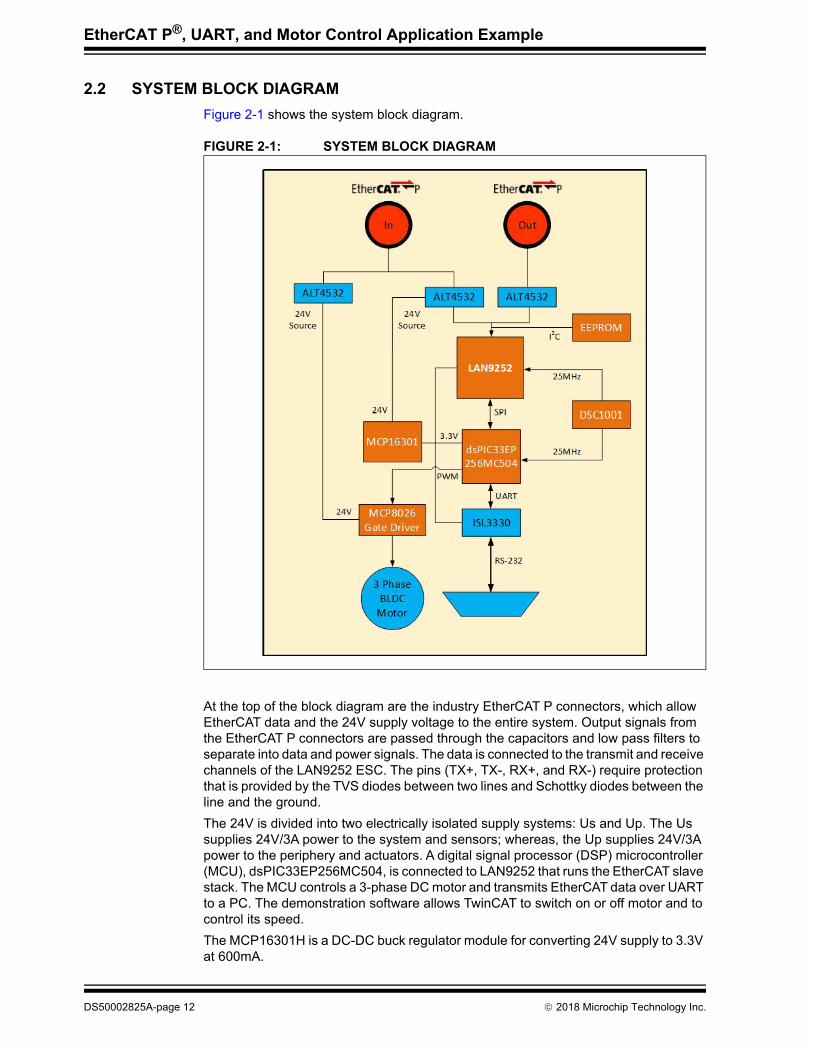
2.2 SYSTEM BLOCK DIAGRAM
Figure 2-1 shows the system block diagram.
FIGURE 2-1: SYSTEM BLOCK DIAGRAM
At the top of the block diagram are the industry EtherCAT P connectors, which allow EtherCAT data and the 24V supply voltage to the entire system. Output signals from the EtherCAT P connectors are passed through the capacitors and low pass filters to separate into data and power signals. The data is connected to the transmit and receive channels of the LAN9252 ESC. The pins (TX+, TX-, RX+, and RX-) require protection that is provided by the TVS diodes between two lines and Schottky diodes between the line and the ground.
The 24V is divided into two electrically isolated supply systems: Us and Up. The Us supplies 24V/3A power to the system and sensors; whereas, the Up supplies 24V/3A power to the periphery and actuators. A digital signal processor (DSP) microcontroller (MCU), dsPIC33EP256MC504, is connected to LAN9252 that runs the EtherCAT slave stack. The MCU controls a 3-phase DC motor and transmits EtherCAT data over UART to a PC. The demonstration software allows TwinCAT to switch on or off motor and to control its speed.
The MCP16301H is a DC-DC buck regulator module for converting 24V supply to 3.3V at 600mA.
DS50002825A-page 12 2018 Microchip Technology Inc.
ETHERCAT P®, UART,AND MOTOR CONTROL
APPLICATION EXAMPLE
Chapter 3. Schematics Design
®
3.1 ETHERCAT P SCHEMATICS3.1.1 LAN9252
Component selection starts by looking at the list of the requirements to identify compo-nents that could be used for the application. At the center of the design is a LAN9252 ESC.
The LAN9252 is used for this design because it is an EtherCAT slave transceiver with dual integrated PHYs. It supports 4-process data interfaces: SPI, SQI, HBI, and a 16-bit digital I/O. This design uses the SPI bus because it provides a low pin count synchro-nous slave interface that facilitates communication between LAN9252 ESC and dsPIC MCU.
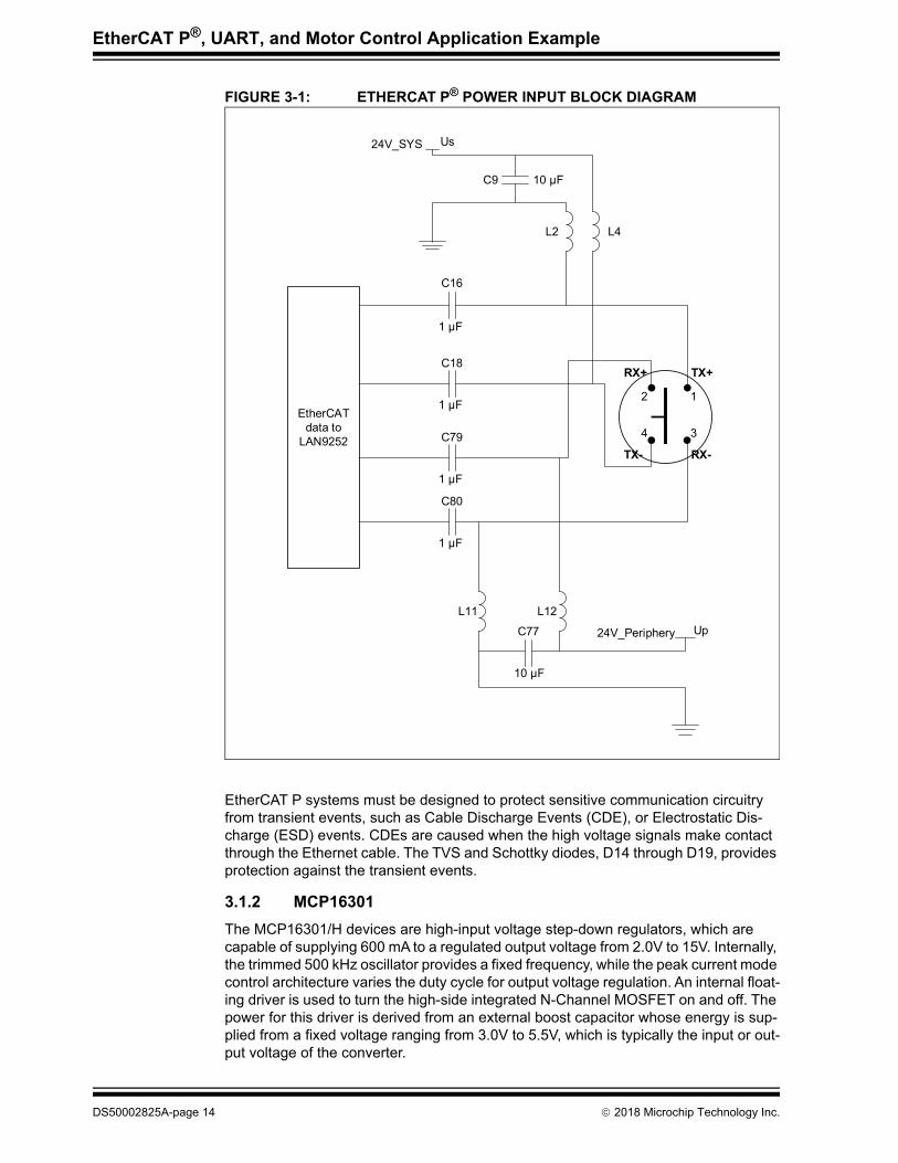
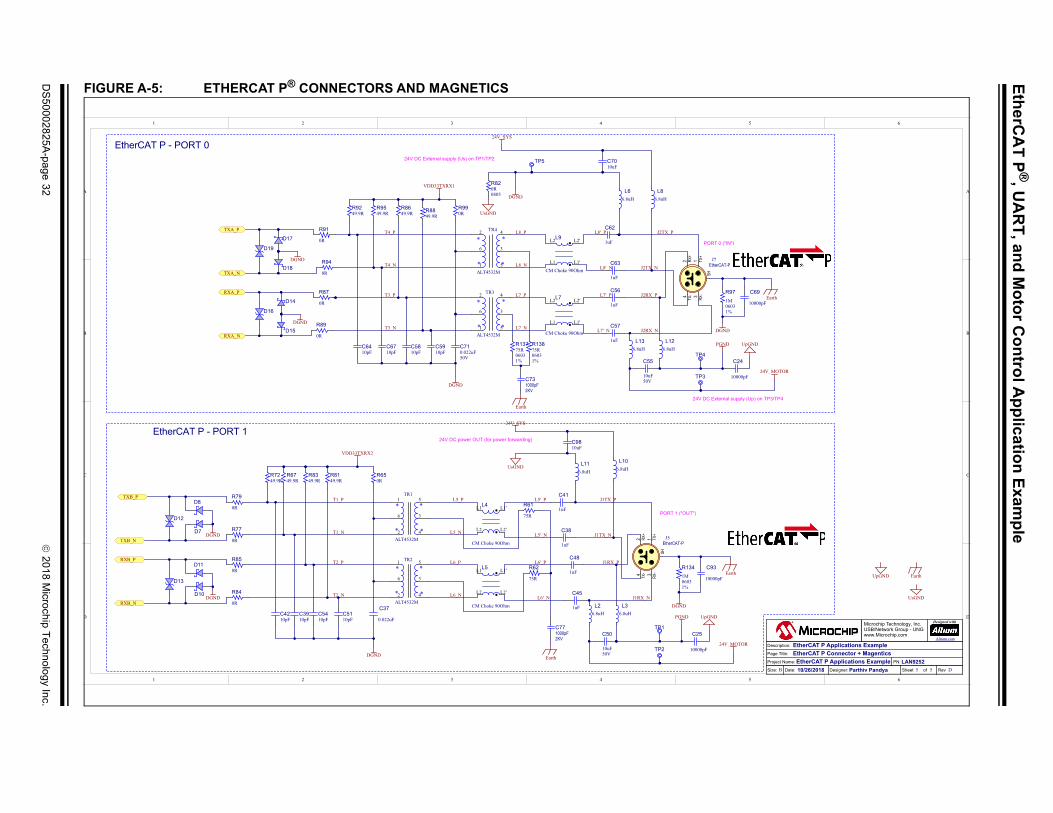
Based on the EtherCAT P standard requirements, the signals received over the Ether-CAT P interface should be split into data and power lines. The data is transmitted to the ESC and two separate power signals of 24V/3A each is supplied to the internal circuitry, external sensors (Us), and local actors (Up). Figure 3-1 shows the block diagram of the arrangement. As shown in Appendix A. “Schematics”, L2, L4, C9, L11, L12, and C77 form second order LC filters. These filters separate the 24V DC supply voltage. Capac-itors C16, C18, C79, and C80 blocks the DC voltage.
2018 Microchip Technology Inc. DS50002825A-page 13
EtherCAT P®, UART, and Motor Control Application Example
FIGURE 3-1: ETHERCAT P® POWER INPUT BLOCK DIAGRAM
EtherCAT P systems must be designed to protect sensitive communication circuitry from transient events, such as Cable Discharge Events (CDE), or Electrostatic Dis-charge (ESD) events. CDEs are caused when the high voltage signals make contact through the Ethernet cable. The TVS and Schottky diodes, D14 through D19, provides protection against the transient events.
3.1.2 MCP16301
The MCP16301/H devices are high-input voltage step-down regulators, which are capable of supplying 600 mA to a regulated output voltage from 2.0V to 15V. Internally, the trimmed 500 kHz oscillator provides a fixed frequency, while the peak current mode control architecture varies the duty cycle for output voltage regulation. An internal float-ing driver is used to turn the high-side integrated N-Channel MOSFET on and off. The power for this driver is derived from an external boost capacitor whose energy is sup-plied from a fixed voltage ranging from 3.0V to 5.5V, which is typically the input or out-put voltage of the converter.
EtherCAT data to
LAN9252
24V_SYS Us
C9 10 µF
L2 L4
C16
1 µF
C18
1 µF
C79
1 µF
C80
1 µF
L11 L12
C77
10 µF
24V_Periphery Up
RX+
TX-
TX+
RX-
2
4 3
1
DS50002825A-page 14 2018 Microchip Technology Inc.
Schematics Design
The MCP16301 integrates an N-Channel MOSFET. A high-side supply is needed to drive the gate of the N-Channel MOSFET above the input voltage to turn it on. This example uses the 3.3V output voltage to charge the boost capacitor (C4) while the inductor current flows, clamping the SW node to a diode drop below ground. Prior to startup, there is no inductor current, so an internal precharged circuit charges the boost cap up to a minimum threshold. Once C4 is charged, NMOS can be turned on, ramping current into the inductor. The D1 diode is used to provide a charging path for the C4 capacitor, while current is flowing through the inductor.
The R1 and R3 sense resistors set the output at 3.3V according to Equation 3-1.
EQUATION 3-1:
Where, VFB = 0.8V is the reference voltage of the FB pin.
The external divider resistors have no effect on system gain, so a wide range of values can be used. A 10 k resistor is recommended as a good trade-off for quiescent cur-rent and noise immunity.
Internally, approximately half of the inductor current downslope is summed with the internal current sense signal. For the proper amount of slope compensation, it is rec-ommended to keep the inductor downslope current constant by varying the inductance with VOUT. For the 3.3V output, a 15 µH inductor is recommended.
The input capacitor must filter the high-input ripple current because of pulsing or chop-ping the input voltage. A low Equivalent Series Resistance (ESR), preferably a ceramic capacitor, is recommended. The necessary capacitance is dependent on the maximum load current and source impedance. Minimum capacitance at light load is 2.2 µF.
The output capacitor helps in providing a stable output voltage during sudden load tran-sients and reduces the output voltage ripple. The minimum value of the output capaci-tance is limited to 20 µF, due to the integrated compensation of the MCP16301.
The freewheeling diode creates a path for inductor current flow after the internal switch is turned off. The efficiency of the converter is a function of the forward drop voltage value and speed of the freewheeling Schottky diode.
For detailed information, see the MCP16301 Data Sheet (DS25004).
3.1.3 dsPIC33EP256MC504
The dsPIC33EP256MC504 MCU runs the EtherCAT slave stack. It receives data and command from the EtherCAT master and controls the external motor by outputting three sets of PWM signals for the 3-phase BLDC motor. According to the system requirements, the MCU also implements bridging between EtherCAT and RS232 inter-faces.
3.1.4 MCP8026
The MCP8026 is a 3-phase brushless DC (BLDC) motor gate driver with integrated power module. Along with the dsPIC33EP256MC504 MCU, it provides the necessary drive signals to drive a 3-phase BLDC motor. The MCP8026 contains the high-side and low-side drivers for external N-channel MOSFETs. The dsPIC MCU supplies the PWM inputs to the MCP8026.
The major internal blocks of this device include a voltage bias generator and a motor control unit.
RTOP RBOT VOUT VFB 1– =
2018 Microchip Technology Inc. DS50002825A-page 15
EtherCAT P®, UART, and Motor Control Application Example
3.1.4.1 BIAS GENERATOR
MCP8026 contains two internal low drop outs (LDOs), 5V and 12V output voltage, and an internal buck switch mode power supply (SMPS).
The 5V rail is used for bias of the internal current sense amplifier and the gate control. A minimum of 4.7 µF ceramic output capacitance is required for the 5V LDO.
The 12V rail is used for bias of the 3-phase power MOSFET bridge. It can supply up to 30 mA of load current. A 10 µF ceramic output capacitance is required for the 12V LDO.
The internal SMPS is capable of supplying 750 mW of power to an external load at 460 kHz switching frequency with an input voltage of 6V. An external inductor is used at the LX pin for the SMPS block.
The maximum inductor value for the operation in discontinuous conduction mode can be determined by using Equation 3-2.
EQUATION 3-2:
Using the LMAX inductor value ensures discontinuous conduction mode operation for output load currents below the critical current level, Iocrit.
An internally unregulated charged pump is utilized to boost the input to the 12V LDO during low input conditions. A typical charge pump flying capacitor (C29 and C30 as shown in Figure A-3) is a 0.1-1.0 µF ceramic capacitor.
The device has an internal temperature sensor. If the temperature rises above the threshold, all functions are turned off and the device signals the MCU using the DE2 pin. The MCU should take the appropriate action.
3.1.4.2 MOTOR CONTROL
Each motor phase is driven with external NMOS/PMOS MOSFET pairs. A low-side and a high-side gate driver control these MOSFET pairs. The gate drivers are controlled directly by the digital input pins PWM[1:3]H/L. A logic high turns the associated gate driver on, and a logic low turns the associated gate driver off. The PWM[1:3]H/L digital inputs are equipped with internal pull-down resistors. The low-side gate drivers are biased by the 12V LDO output. The high-side gate drivers are a floating drive biased by a bootstrap capacitor circuit. The bootstrap capacitor is charged by 12V LDO when-ever the accompanying low-side MOSFET is turned on.
For detailed information, see the MCP8026 Data Sheet (DS20005905). It shows the detailed component calculations.
LMAX Vo 1 V0– Vin T 2 locrit
DS50002825A-page 16 2018 Microchip Technology Inc.
ETHERCAT P®, UART,AND MOTOR CONTROL
APPLICATION EXAMPLE
Chapter 4. PCB Layout
4.1 INTRODUCTION
Input to the PCB layout process includes component signal connectivity (netlist), mechanical requirements, and electrical constraints. As part of the electrical con-straints, signals that need special attention include high frequency signals, high power rails, and analog signals.
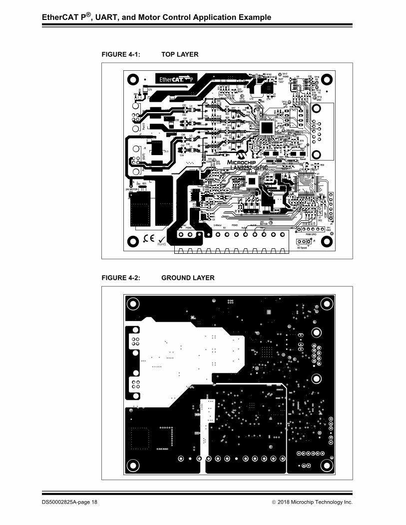
All the VDD pins should directly be routed into a solid +3.3V power plane, and the pin-to-plane trace should be short and wide. All the decoupling capacitors should be placed near the VDD pins and should have short and direct connections to each power plane (+3.3V and digital ground plane). The VDDCR pins must be routed with a heavy, wide trace with multiple vias to the three decoupling capacitors and the single bulk capacitor associated with it. All three pins and the capacitors should be routed directly into a solid, +1.2V power plane. The digital and analog ground pins should be tied together and should be connected directly into a solid, contiguous, internal ground plane.
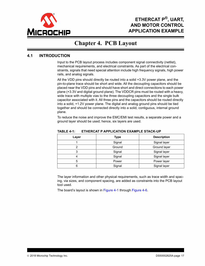
To reduce the noise and improve the EMC/EMI test results, a separate power and a ground layer should be used; hence, six layers are used.
The layer information and other physical requirements, such as trace width and spac-ing, via sizes, and component spacing, are added as constraints into the PCB layout tool used.
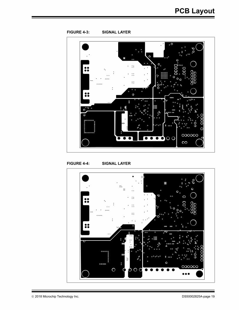
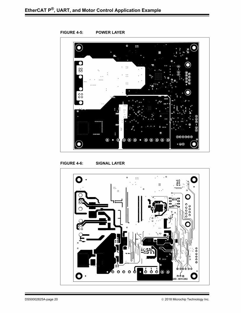
The board’s layout is shown in Figure 4-1 through Figure 4-6.
TABLE 4-1: ETHERCAT P APPLICATION EXAMPLE STACK-UP
Layer Type Description
1 Signal Signal layer
2 Ground Ground layer
3 Signal Signal layer
4 Signal Signal layer
5 Power Power layer
6 Signal Signal layer
2018 Microchip Technology Inc. DS50002825A-page 17
EtherCAT P®, UART, and Motor Control Application Example
FIGURE 4-1: TOP LAYER
FIGURE 4-2: GROUND LAYER
DS50002825A-page 18 2018 Microchip Technology Inc.
PCB Layout
FIGURE 4-3: SIGNAL LAYER
FIGURE 4-4: SIGNAL LAYER
2018 Microchip Technology Inc. DS50002825A-page 19
EtherCAT P®, UART, and Motor Control Application Example
FIGURE 4-5: POWER LAYER
FIGURE 4-6: SIGNAL LAYER
DS50002825A-page 20 2018 Microchip Technology Inc.
PCB Layout
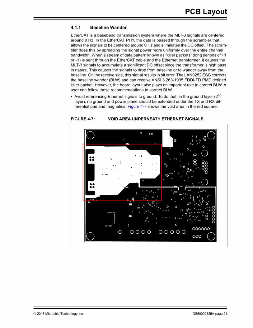
4.1.1 Baseline Wander
EtherCAT is a baseband transmission system where the MLT-3 signals are centered around 0 Hz. In the EtherCAT PHY, the data is passed through the scrambler that allows the signals to be centered around 0 Hz and eliminates the DC offset. The scram-bler does this by spreading the signal power more uniformly over the entire channel bandwidth. When a stream of data pattern known as “killer packets” (long periods of +1 or -1) is sent through the EtherCAT cable and the Ethernet transformer, it causes the MLT-3 signals to accumulate a significant DC offset since the transformer is high pass in nature. This causes the signals to drop from baseline or to wander away from the baseline. On the receive side, this signal results in bit error. The LAN9252 ESC corrects the baseline wander (BLW) and can receive ANSI 3 263-1995 FDDI-TD PMD defined killer packet. However, the board layout also plays an important role to correct BLW. A user can follow these recommendations to correct BLW.
• Avoid referencing Ethernet signals to ground. To do that, in the ground layer (2nd layer), no ground and power plane should be extended under the TX and RX dif-ferential pair and magnetics. Figure 4-7 shows the void area in the red square.
FIGURE 4-7: VOID AREA UNDERNEATH ETHERNET SIGNALS
2018 Microchip Technology Inc. DS50002825A-page 21
EtherCAT P®, UART, and Motor Control Application Example
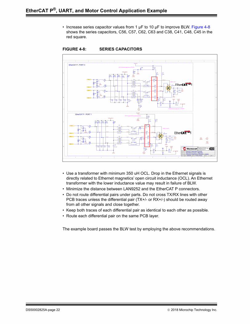
• Increase series capacitor values from 1 µF to 10 µF to improve BLW. Figure 4-8 shows the series capacitors, C56, C57, C62, C63 and C38, C41, C48, C45 in the red square.
• Use a transformer with minimum 350 uH OCL. Drop in the Ethernet signals is directly related to Ethernet magnetics’ open circuit inductance (OCL). An Ethernet transformer with the lower inductance value may result in failure of BLW.
• Minimize the distance between LAN9252 and the EtherCAT P connectors.
• Do not route differential pairs under parts. Do not cross TX/RX lines with other PCB traces unless the differential pair (TX+/- or RX+/-) should be routed away from all other signals and close together.
• Keep both traces of each differential pair as identical to each other as possible.
• Route each differential pair on the same PCB layer.
The example board passes the BLW test by employing the above recommendations.
FIGURE 4-8: SERIES CAPACITORS
1
1
2
2
3
3
4
4
5
5
6
6
D D
C C
B B
A A
Page Title:
Project Name:
EtherCAT P Connector + MagenticsEtherCAT P Applications Example PN: LAN9252
Description:
Date:Size: Sheet of RevB 5 5 D10/26/2018 Designer: Parthiv Pandya
EtherCAT P Applications Example
Designed withMicrochip Technology, Inc.USB/Network Group - UNGwww.Microchip.com
Altium.com
VDD33TXRX1
0.022uF50V
C71
L2 L2'
L1 L1'
CM Choke 90Ohm
L9
L2 L2'
L1 L1'
CM Choke 90Ohm
L7
75R06031%
R13775R06031%
R138
VDD33TXRX2
0.022uF
C37
L2 L2'
L1 L1'
CM Choke 90Ohm
L4
L2 L2'
L1 L1'
CM Choke 90Ohm
L5
75R
R61
75R
R62
1uF
C62
1uF
C63
1uF
C56
1uF
C57
24V_SYS
49.9RR72
49.9RR67
49.9RR83
49.9RR81
49.9RR92
49.9RR95
49.9RR86
49.9RR88
0RR65
0RR99
Earth
Earth
1uF
C41
1uF
C38
1uF
C48
1uF
C45
Earth
Earth
PORT 1 ("OUT")
PORT 0 ("IN")
EtherCAT P - PORT 0
EtherCAT P - PORT 124V DC power OUT (for power forwarding)
1M06031%
R134
10000pF
C93
1M06031%
R97
10000pF
C69
10pFC64
10pFC67
10pFC58
10pFC59
10pFC42
10pFC39
10pFC54
10pFC51
10uFC70
10uF50V
C55
TXA_N
TXA_P
RXA_N
RXA_P
TXB_N
TXB_P
RXB_N
RXB_P
24V_MOTOR
T4_P
T4_N
T3_P
T3_N
L8_P
L8_N
L7_P
L7_N
T1_P
T1_N
T2_P
T2_N
L5_P
L5_N
L6_P
L6_N
0R
R91
0R
R94
0R
R87
0R
R89
0R
R79
0R
R77
0R
R85
0R
R84
D19
D16
D12
D13
L8'_P
L8'_N
L7'_P
L7'_N
J2TX_P
J2TX_N
J2RX_P
J2RX_N
L5'_P
L5'_N
L6'_P
L6'_N
J1TX_P
J1TX_N
J1RX_P
J1RX_N
TP4
24V DC External supply (Us) on TP1/TP2 TP5
TP3
UpGND
24V DC External supply (Up) on TP3/TP4
DGND
DGND
DGND
DGND
UsGND
10uFC98
24V_SYS
UsGND
UsGND
UpGND Earth
DGND
PGND
10000pF
C24
10uF50V
C50
24V_MOTOR
TP1
TP2
UpGNDPGND
10000pF
C25
DGND
DGND
DGND
DGND
D17
D18
D14
D15
D8
D7
6
2
51
*
* *
3
4
*
ALT4532M
TR4
6
2
51
*
* *
3
4
*
ALT4532M
TR3
6
2
51
*
* *
3
4*ALT4532M
TR1
6
2
51
*
* *
3
4*ALT4532M
TR2
6.8uH
L66.8uH
L8
6.8uH
L126.8uH
L13
6.8uH
L116.8uH
L10
6.8uH
L26.8uH
L3
0R0805
R82
D11
D10
1000pF2KV
C73
1000pF2KV
C77
12
34RX
+
TX+
TX-
RX-
SH
EtherCAT-PJ5
12
34RX
+
TX+
TX-
RX-
SH
EtherCAT-PJ7
DS50002825A-page 22 2018 Microchip Technology Inc.
ETHERCAT P®, UART,AND MOTOR CONTROL
APPLICATION EXAMPLE
Chapter 5. Software
®
5.1 ETHERCAT P SOFTWARE REQUIREMENTSSeveral software components are required, including dsPIC33 SDK, EEPROM pro-gramming, and a system application.
5.1.1 dsPIC33 SDK
The dsPIC33 SDK is an EtherCAT software stack for the LAN9252 device written for the dsPIC33 device. The SDK implements the EtherCAT slave functions that can com-municate with the EtherCAT master.
The SDK is available from www.microchip.com web site. It includes a quick start guide that explains the steps to:
1. Install TwinCAT (EtherCAT master) drivers on a PC that acts as an EtherCAT master
2. Generate the slave source files using the SSC® tool
3. Integrate dsPIC33EP256MC504 MCU configuration files in the slave source files generated in step 2
4. Compile the MPLAB X® IDE based project and program it on a demo board
5. Scan the EtherCAT slave device from TwinCAT
6. Program EEPROM with ESI
7. Run the example
There are several source files required to develop the EtherCAT slave project. To speed up the process, the EtherCAT.org web site provides the SSC tool, which uses a graphical user interface or GUI-based approach to select the required parameters to generate the source files.
5.1.2 EEPROM Programming
Once the SDK is programmed on the dsPIC MCU, the system requires that the on-board EEPROM be programmed with EtherCAT Slave Information (ESI). When the system starts, the EtherCAT master, TwinCAT in this case, reads the LAN9252 ESC profile using the LAN9252’s internal register.
2018 Microchip Technology Inc. DS50002825A-page 23
EtherCAT P®, UART, and Motor Control Application Example
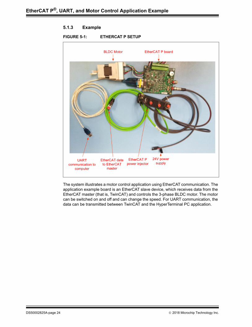
5.1.3 Example
The system illustrates a motor control application using EtherCAT communication. The application example board is an EtherCAT slave device, which receives data from the EtherCAT master (that is, TwinCAT) and controls the 3-phase BLDC motor. The motor can be switched on and off and can change the speed. For UART communication, the data can be transmitted between TwinCAT and the HyperTerminal PC application.
FIGURE 5-1: ETHERCAT P SETUP
BLDC Motor EtherCAT P board
24V power supply
EtherCAT P power injector
EtherCAT data to EtherCAT
master
UART communication to
computer
DS50002825A-page 24 2018 Microchip Technology Inc.
ETHERCAT P®, UART,AND MOTOR CONTROL
APPLICATION EXAMPLE
Chapter 6. Hardware Testing
6.1 INTRODUCTION
During hardware testing, the various system functional blocks should be verified, start-ing with the power supply.
6.1.1 Power Supply
The MCP16301H input voltage should be tested for the correct 24V supply voltage. Confirm that the output voltage is 3.3V using a digital voltmeter. Also, confirm 3.3V sup-ply voltage to all the digital ICs such as, dsPIC33EP256MC504, MCP8026, LAN9252, and so on. The power supply verification should include verifying the voltage, ripple, and operation under various load conditions, including the maximum rated load.
6.1.2 dsPIC33EP256MC504
A simple software routine should be done on the MCU to test the following parts:
• On-board debug LED. This LED can be used to test if the MCU is running. A small program can be run on the MCU, which causes the debug LED to blink at a partic-ular frequency. This test validates that the MCU is programmed successfully and working properly.
• UART. Successful transmission and reception of data from a PC to the ESC con-firms that the UART connections are correct.
• Motor control. Correct connections and component selection for the motor control circuit must be ensured.
Once correct operation of individual parts is verified, the software SDK should be pro-grammed on the board and tested for the complete functionality.
2018 Microchip Technology Inc. DS50002825A-page 25
EtherCAT P®, UART, and Motor Control Application Example
NOTES:
DS50002825A-page 26 2018 Microchip Technology Inc.
ETHERCAT P®, UART,AND MOTOR CONTROL
APPLICATION EXAMPLE
Appendix A. Schematics
This appendix shows the schematics of the EtherCAT P board.
2018 Microchip Technology Inc. DS50002825A-page 27
Eth
erCA
T P
®, U
AR
T, an
d M
oto
r Co
ntro
l Ap
plic
ation
Exam
ple
DS
50002825A
-page 28
2018 M
icrochip Technolo
gy Inc.
5
5
6
6
D
C
B
A
Page Title:
Project Name:
Block DiagramEtherCAT P Applications Example PN: LAN9252
Description:
Date:Size: Sheet of RevB 1 5 D10/26/2018 Designer: Parthiv Pandya
EtherCAT P Applications Example
Designed withMicrochip Technology, Inc.USB/Network Group - UNGwww.Microchip.com
Altium.com
Revision Summary Author
nts
nctional
m
unctional
vers + UART + 3V3Regulator
onnector + Magnetics
FIGURE A-1: ETHERCAT P® APPLICATION EXAMPLE BLOCK DIAGRAM
1
1
2
2
3
3
4
4
D
C
B
A
Revision HistoryRevision Date
EtherCAT P Application Example Board
Table of Conte
1
DescriptionSheet
2
3
LAN9252 Fu
Block Diagra
dsPIC33EP F
Block Diagram
4
5
MOSFET dri
EtherCAT P C
Sch
ematics
2018
Microchip T
echnology Inc.D
S5
0002825A-p
age 29
FIG
5
5
6
6
D D
C C
B B
A A
Page Title:
Project Name:
LAN9252 FunctionalEtherCAT P Applications Example PN: LAN9252
Description:
Date:Size: Sheet of RevB 2 5 D10/26/2018 Designer: Parthiv Pandya
EtherCAT P Applications Example
Designed withMicrochip Technology, Inc.USB/Network Group - UNGwww.Microchip.com
Altium.com
0.1uFC46
URE A-2: LAN9252 STRAP AND EEPROM CONNECTIONS
1
1
2
2
3
3
4
4
STB1
GND2
OUT3
VDD4
STBGND
OUTVDD
DSC1001
U3
CLK_25
12.1kR136
3V3
LAN9252_IRQ
3V3
VDDCR
TXA_NTXA_PRXA_NRXA_P
3V3
3V3
3V3
TXB_NTXB_PRXB_NRXB_P
I2C_SCLI2C_SDA
dsPIC_SCK
dsPIC_MISOdsPIC_MOSI
VDD12TX
3V3 VDDCR
VDD33TXRX1VDD33TXRX2
VDD12TX
dsPIC_SS
3V3
51R
R68RST#
220OHM
FB4
3V3
100Base - FX LOS Enable
Loss Of Signal mode is enabled for both PHY A and PHY B
rxa_n
Fixed EEPROM address "000"
rxa_p
txa_ptxa_n
rxb_nrxb_p
txb_ptxb_n
Power Supply Filtering
VDD33TXRX1
VDD33TXRX2
1uFC100
1uFC105
TP14TP17Put this TestPoint close to IRQ Testpoint
Sync1Sync0
0.012uFC60
0.012uFC52
0.012uF
C47
1uFC65
1uFC44
10k
DNP
R73
10k
R74
4.7kR93
4.7kR90
10k
R135
10kR76
GREEN
D21
GREEN
D22
GREEN
D23
LINK/ACT LED PORT 0
LINK/ACT LED PORT 1
RUN LED
chip_mode_strap[1:0] = 00 (2 Port mode)
LED Straps
1k
R118
1k
R119
1k
R96
GPIO0
GPIO1
GPIO2
GPIO0GPIO1
GPIO2
3V3
0.1uFC40
TP10
TP11
TP8
TP9
SCK
SS
SDI
SDO
0.1uFC66
A01
SDA5
A23
A12
WP7
VSS4
SCL6
VCC8
24FC512T
DNPU9
0.1uFC102
0.1uFC101
0.1uFC49
0.1uFC53
0.1uFC61
0.1uFC104 0.1uF
C1061uFC103
DGND
DGND
DGND DGND DGND DGND
DGND DGND
DGND
DGND
DGND
DGND
DGND
DGND DGND
DGNDDGND
DGND
DGND
DGND
DGND
DGND DGND
DGND DGND1k
R112
1k
R111
1k
R110
220OHM
FB2
220OHM
FB5
220OHMFB3
Place R127 near U3
DGND
12
DNP
TP7
A01
SDA5
A23
A12
WP7
VSS4
SCL6
VCC8
24FC512T
U10
DGND
3V3
RBIAS57
OSCI1
OSCO2
OSCVDD123
OSCVSS4
REG_EN7
FXLOSEN8
RST_n11
IRQ44
TESTMODE41
LINKACTLED0/TDO/CHIP_MODE048
LINKACTLED1/TDI/CHIP_MODE146
RUNLED/E2PSIZE45
EESCL/TCK43
EESDA/TMS42
FXSDA/FXLOSA/FXSDENA9
FXSDB/FXLOSB/FXSDENB10
TXNA52
TXPA53
RXNA54
RXPA55
RXPB60
RXNB61
TXPB62
TXNB63
A0/D15/AD15/DIGIO9/GPI9/GPO9/MII_RXER33
D14/AD14/DIGIO8/GPI8/GPO8/MII_TXD3/TX_SHIFT115
D13/AD13/DIGIO7/GPI7/GPO7/MII_TXD2/TX_SHIFT016
D12/AD12/DIGIO6/GPI6/GPO6/MII_TXD121
D11/AD11/DIGIO5/GPI5/GPO5/MII_TXD022
D10/AD10/DIGIO4/GPI4/GPO4/MII_TXEN23
D9/AD9/LATCH_IN/SCK19
D8/AD8/DIGIO2/GPI2/GPO2/MII_MDIO40
D7/AD7/DIGIO1/GPI1/GPO1/MII_MDC39
D6/AD6/DIGIO0/GPI0/GPO0/MII_RXCLK36
D5/AD5/OUTVALID/SCS#50
D3/AD3/WD_TRIG/SIO335
D2/AD2/SOF/SIO212
D1/AD1/EOF/SO/SIO113
D0/AD0/WD_STATE/SI/SIO017
D4/AD4/DIGIO3/GPI3/GPO3/MII_LINK49
A4/DIGIO12/GPI12/GPO12/MII_RXD027
A3/DIGIO11/GPI11/GPO11/MII_RXDV26
A2/ALEHI/DIGIO10/GPI10/GPO10/LINKACTLED2/MII_LINKPOL29
A1/ALELO/OE_EXT/MII_CLK2525
RD/RD_WR/DIGIO15/GPI15/GPO15/MII_RXD331
WR/ENB/DIGIO14/GPI14/GPO14/MII_RXD230
CS/DIGIO13/GPI13/GPO13/MII_RXD128
SYNC1/LATCH118
SYNC0/LATCH034
RBIAS
OSCIOSCO
OSCVDD12
OSCVSS
REG_EN
FXLOSEN
RST_nIRQ
TESTMODE
LINKACTLED0/TDO/CHIP_MODE0LINKACTLED1/TDI/CHIP_MODE1
RUNLED/E2PSIZE
EESCL/TCKEESDA/TMS
FXSDA/FXLOSA/FXSDENA
FXSDB/FXLOSB/FXSDENB
TXNATXPA
RXNARXPA
RXPBRXNBTXPBTXNB
A0/D15/AD15/DIGIO9/GPI9/GPO9/MII_RXERD14/AD14/DIGIO8/GPI8/GPO8/MII_TXD3/TX_SHIFT1
D13/AD13/DIGIO7/GPI7/GPO7/MII_TXD2/TX_SHIFT0D12/AD12/DIGIO6/GPI6/GPO6/MII_TXD1D11/AD11/DIGIO5/GPI5/GPO5/MII_TXD0D10/AD10/DIGIO4/GPI4/GPO4/MII_TXEN
D9/AD9/LATCH_IN/SCKD8/AD8/DIGIO2/GPI2/GPO2/MII_MDIOD7/AD7/DIGIO1/GPI1/GPO1/MII_MDC
D6/AD6/DIGIO0/GPI0/GPO0/MII_RXCLK
D5/AD5/OUTVALID/SCS#
D3/AD3/WD_TRIG/SIO3D2/AD2/SOF/SIO2
D1/AD1/EOF/SO/SIO1D0/AD0/WD_STATE/SI/SIO0AA
D4/AD4/DIGIO3/GPI3/GPO3/MII_LINK
A4/DIGIO12/GPI12/GPO12/MII_RXD0A3/DIGIO11/GPI11/GPO11/MII_RXDV
A2/ALEHI/DIGIO10/GPI10/GPO10/LINKACTLED2/MII_LINKPOLA1/ALELO/OE_EXT/MII_CLK25
RD/RD_WR/DIGIO15/GPI15/GPO15/MII_RXD3WR/ENB/DIGIO14/GPI14/GPO14/MII_RXD2
CS/DIGIO13/GPI13/GPO13/MII_RXD1
SYNC1/LATCH1SYNC0/LATCH0
INTERRUPT/RESET PORTA Twisted Pair
PORTB Twisted Pair
POWER
MISC
OSCILLATOR
I2C/JTAG
STRAPS/MISC
AD[15:0]/DIGIO[15:0] / GPI/15:0]/GPO[15:0]/MII
VDD33BIAS58
VDD335
VDDIO114
VDDIO220
VDDIO332
VDDIO437
VDDIO547
VDD33TXRX151
VDD33TXRX264
VDD12TX156
VDD12TX259
VDDCR16
VDDCR224
VDDCR338
ePAD65
LAN9252U6
DGND
10kDNPR114
Eth
erCA
T P
®, U
AR
T, an
d M
oto
r Co
ntro
l Ap
plic
ation
Exam
ple
DS
50002825A
-page 30
2018 M
icrochip Technolo
gy Inc.
5
5
6
6
D
C
B
A
Page Title:
Project Name:
dsPIC33EP_FunctionalEtherCAT P-Applications Example PN: LAN9252
Description:
Date:Size: Sheet of RevB 3 5 D10/26/2018 Designer: Parthiv Pandya
EtherCAT P-Applications Example
Designed withMicrochip Technology, Inc.USB/Network Group - UNGwww.Microchip.com
Altium.com
V12
PGND PGND
VBA VBB VBC
PGND
PGND
HS2HS1HS0
VBAVBBVBC
V12
PGND
PGNDLX
HS0HS1HS2
V5
HALLAHALLBHALLC
PGND
AV33
AGND
V33AV33
AGND
FB
U_Motor V_Motor W_Motor
PG
ND
10RR18
10RR2010RR19
B26
A27
B29
A30
B32
A33
D35
D36
C25
C28
C31
O34
10kR42
10kR43
AGND
SMF33AT1GDNP
D3SMF33AT1GDNP
D2SMF33AT1GDNP
D1
0.1uF
C22
1uFC90
1uFC88
1uFC89
V5
PGND
0R
DNP
R46
10uF16
C3210uF16
C6
DGND
F
DGND
DGND
2.2uF10V0603
C26
U_MotorV_MotorW_Motor
24V_MOTORPGND
Motor Position Signals and Hall Sensors
L1
15uH
Moto
rP
osi
tio
nS
ign
als
and
Hal
lS
enso
rs
24V_MOTOR
10uFC20
1N5819HW-7-FD24
1N5819HW-7-FD25
1N5819HW-7-FD26
1.8kR51
1.1kR44
1N5819HW-7-FD4
4.7uFC91
rence
2
1
3
FDD1
0AN0
6A0
Q7
PGND
SMAJ24A-E3/61D29
PGND
10kR113
11
2
3
4
5
6
7
8
9
10
11
12
J1
15uF50V
C21
w designs.
2627
2930
3233
3536
25
28
31
34
BA
BA
BA
DD
C
C
C
O
FIGURE A-3: DSPIC33EP FUNCTIONAL AND MOTOR CONTROL
1
1
2
2
3
3
4
4
D
C
B
A
MotorGateDrv_CE
I_OUT3I_SENSE3-I_SENSE3+I_OUT2
I_S
EN
SE
2-
I_S
EN
SE
2+
Moto
rGat
eDrv
_IL
IMIT
_O
UT
LS
0L
S1
LS
2
V5
V33
ADBUS
VBUS Monitor
HALLA HALLA_F
HALLB_F
HALLC_F
DGND
HALLB
HALLC
Filtered Motor Position Sensor Signals
FB
AD_SPEED
PHA
PHB
PHC
Terminal Voltage Sensing
PGND
ISPCLKISPDATA
V33
ICSP
DGND
PGND
Motor Controller Power (24V Nominal)
VREF 1/2 VDD = 1.65V
VREF
AGND
I_SENSE1+
I_OUT1
DGND
AGND
PGND
I_SENSE3+
I_SENSE3- I_OUT3
Differential Current Amplifier Gain = 15
I_OUT2
I_SENSE2+
VREF
I_SENSE2-
Differential Current Amplifier Gain = 15
DGND
LX
LS
0L
S1
LS
2
U_Motor
IPHASEA+IPHASEB+
V_Motor
W_Motor
I_O
UT
1
I_S
EN
SE
1+
I_S
EN
SE
1-
PG
ND
PG
ND
PG
ND
PGND
DE2
300RR25
300RR6
300RR49
12kR8
12kR12
12kR47
1k
R24
1k
R13
1kR48
20kR22
1kR21
1k
R36
1k
R37
1k
R39
1k
R40
47kR29
200R
R26
EP
49
ISE
NS
E2-
13
PW
M2H
48
/IL
IMIT
15
IOU
T1
16
PW
M3H
46
PW
M3L
45
ISE
NS
E+
18
PG
ND
19
CA
P1
43
CA
P2
42
LA
21
LB
22
FB
40
VD
D39
PG
ND
24
LX
37
PGND7
LV_OUT18
HV_IN25
LV_OUT24
PWM1H2
PWM1L1
HH
PHPH
VBVB
PGNPGN
IOUT212
IOUT39
CE3
HV_IN16
ISE
NS
E2+
14
ISE
NS
E1-
17
PG
ND
20
LC
23
PW
M2L
47
DE
244
5V
LD
O41
VD
D38
H
PH
VB
12VLD
ISENSE3+11
ISENSE3-10
MCP8026
U2
PGND
TMS/ASDA1/RP41/RB91
RP54/RC62
RP55/RC73
RP56/RC84
RP57/RC95
VSS6
VCAP7
RP42/PWM3H/RB108
RP43/PWM3L/RB119
RPI44/PWM2H/RB1210
RPI45/PWM2L/CTPLS/RB1311
TDO/RA1012
TDI/RA713
RPI46/PWM1H/T3CK/RB1414
RPI47/PWM1L/T5CK/RB1515
AVSS16
AVDD17
MCLR18
AN0/OA2OUT/RA019
AN1/C2IN1+/RA120
PGED3/VREF-/AN2/C2IN1-/SS1/RPI32/CTED2/RB021
PGEC3/VREF+/AN3/OA1OUT/RPI33/CTED1/RB122
PGEC1/AN4/C1IN1+/RPI34/RB223
PGED1/AN5/C1IN1-/RP35/RB324
AN6/OA3OUT/C4IN1+/OCFB/RC025
AN7/C3IN1-/C4IN1-/RC126
AN8/C3IN1+/U1RTS/BCLK1/FLT3/RC227
VDD28
VSS29
OSC1/CLKI/RA230
OSC2/CLKO/RA331
SDA2/RPI24/RA832
FLT32/SCL2/RP36/RB433
CVREF2O/SDO1/RP20/T1CK/RA434
SDI1/RPI25/RA935
SCK1/RPI51/RC336
SDA1/RPI52/RC437
SCL1/RPI53/RC538
VSS39
VDD40
PGED2/ASDA2/RP37/RB541
PGEC2/ASCL2/RP38/RB642
RP39/INT0/RB743
TCK/CVREF1O/ASCL1/RP40/T4CK/RB844
TMS/ASDA1/RP41/RB9RP54/RC6RP55/RC7RP56/RC8RP57/RC9VSSVCAPRP42/PWM3H/RB10RP43/PWM3L/RB11RPI44/PWM2H/RB12RPI45/PWM2L/CTPLS/RB13TDO/RA10TDI/RA7RPI46/PWM1H/T3CK/RB14RPI47/PWM1L/T5CK/RB15AVSSAAAVDDAAMCLRAN0/OA2OUT/RA0AN1/C2IN1+/RA1PGED3/VREF-/AN2/C2IN1-/SS1/RPI32/CTED2/RB0PGEC3/VREF+/AN3/OA1OUT/RPI33/CTED1/RB1 PGEC1/AN4/C1IN1+/RPI34/RB2
PGED1/AN5/C1IN1-/RP35/RB3AN6/OA3OUT/C4IN1+/OCFB/RC0
AN7/C3IN1-/C4IN1-/RC1AN8/C3IN1+/U1RTS/BCLK1/FLT3/RC2
VDDVSS
OSC1/CLKI/RA2OSC2/CLKO/RA3SDA2/RPI24/RA8
FLT32/SCL2/RP36/RB4CVREF2O/SDO1/RP20/T1CK/RA4
SDI1/RPI25/RA9SCK1/RPI51/RC3SDA1/RPI52/RC4SCL1/RPI53/RC5
VSSVDD
PGED2/ASDA2/RP37/RB5PGEC2/ASCL2/RP38/RB6
RP39/INT0/RB7TCK/CVREF1O/ASCL1/RP40/T4CK/RB8
DSPIC33EP256MC504
U1
AV33
V33
PWM3H/GPIO5PWM3L/GPIO4PWM2H/GPIO3PWM2L/GPIO2
PWM1H/GPIO1PWM1L/GPIO0
PHB
I_OUT2
ADBUS
I_OUT3AD_SPEED
MotorGateDrv_CE
DGND
DE2
MotorGateDrv_ILIMIT_OUT
V33
ISPDATAISPCLK
AGND
dsPIC_SCKdsPIC_MISOdsPIC_MOSI
dsPIC_SSPHC
HALLB_FHALLC_F
LAN9252_IRQSync1
Sync0
HALLA_FU
AR
T_T
x
UART_Tx
UART_Rx
2kR30 DE2
AGND
AGND
PHA
DGNDDGND
4.7uFC36
DGND
0RR16
330RR35
5600pFC17
330RR14
5600pFC13
47kR28
AV33
AGND
V33
DGND
DE2
DGND
100pFC23
VREF
1k
R54
1k
R55
1k
R52
1k
R53100pF
C33
1uFC30
1uFC29
0.1uFC94
1uFC96 1uF
C18
DGND
0.1uFC35
0RR131
0R
R129
0.01uFDNP
C11
0.01uFDNP
C4
0.01uFDNP
C27
2.2uF10V0603
C28
1800pC5
4.99RR7
0.1uFC15
0.1uFC7
10uF50V
C87
PGND
100pF
C8
100pF
C3
100pF
C9
AD Speed
DE2
10kR64
V33
DGND
0.1uF
C16AGND
AGND
90.9kDNP
R990.9kDNP
R390.9kDNP
R11
/MCLR
/MCLR
1k
R60"D11"
D6
DGND
1kR59
"D12"
D5
DGND
4.7k
R754.7kR71
Btn1
V33
1 2
EG4576
SW1
DGND0.1uF
DNP
C43
Btn1
24V_MOTOR
24V_MOTOR
1uF
C31
Indicate pin 1 on PCB
IPHASEB+
AD_SPEED
4.7k
R32
4.7k
R17IPHASEA+
47kR33
10000pFC12
PGND
2.2kR27
V5
4.7kR125
4.7kR124
4.7kR123
IPHASEB- IPHASEA-
30kR58
30kR38
30k
R45
30k
R50
Overcurrent Monitor Plus Debug Input
Debug Input for Speed Setting
Voltage Refe
Buffered VREF
Manual Start/Stop
V33
47kR23
0.1uFC14
DGND
/MCLR
PWM1L/GPIO0
PWM1L/GPIO0PWM1H/GPIO1
PWM1H/GPIO1
PWM2L/GPIO2
PWM2L/GPIO2
PWM2H/GPIO3
PWM2H/GPIO3
PWM3L/GPIO4
PWM3L/GPIO4
PWM3H/GPIO5
PWM3H/GPIO5
PGND PGND
220OHM
FB1
123456
J2
123456
J4
12
J3DGND
V33
470RR10470RR4470RR5
680uF50V
C1
11
2
3
J8
MCU_
TX
Note: MCP8026 is not recommended for the ne
49
13
48
1555
1666
46
45
18
19
43
42
21
22
40
39
24
37
78
54
21
12
9
3
6
14
17
20
23
47
44
41
38
1110
EP
ISE
NS
E2-
PW
M2H
/IL
IMIT
IOU
T1
PW
M3H
PW
M3L
ISE
NS
E+
PG
ND
CA
P1
CA
P2
LA
LB
FB
VD
D
PG
ND
LX
PGNDLV_OUT1LL
HV_IN2LV_OUT2LL
PWM1HPWM1L
HH
PHPH
VBVB
PGNPGN
IOUT2
IOUT3
CE
HV_IN1
ISE
NS
E2+
ISE
NS
E1-
PG
ND
LC
PW
M2L
DE
2
5V
LD
O
VD
D
H
PH
VB
12VLD
ISENSE3+ISENSE3-
MCP8026
U2
9
18
1 16 5
1 13 2
2 20 9
27
1
1 1 2 2
7 4 1 8
11
Sch
ematics
2018
Microchip T
echnology Inc.D
S5
0002825A-p
age 31
FIG
5
5
6
6
D D
C C
B B
A A
Page Title:
Project Name:
MOSFETs + UART + 3V3 RegulatorEtherCAT P Applications Example PN: LAN9252
Description:
Date:Size: Sheet of RevB 4 5 D10/26/2018 Designer: Parthiv Pandya
EtherCAT P Applications Example
Designed withMicrochip Technology, Inc.USB/Network Group - UNGwww.Microchip.com
Altium.com
1
2
3
4
5
6
7
8
9
J6
3V3
For RS-232: Do not populate R84, R98, R100, R104, R107
For RS-485: Do not populate R81, R92, R95, R111
0R DNPR1050RR103
0RR104
0R DNP
R106
0R DNPR107
0R DNP
R108
0R R109
RS-232/485
0.1uF
C84
0.1uF
C107
0.1uF
C78
DGND
DGND
DGNDDGND
FID2Fiducials
FID5 FID4
FID1 FID6 FID3
3V3TP12
TP13
0R
DNPR63
V33
1k
R98
"3V3 Power"
D27
DGND
DGND
10uFC72
10uFC74 31.6k
06031%
R100
DGND
B0540WSD28
DGND
A1
K2
1N4448
D20
DGND DGND
0.1uFC68
15uH
L14
10kR102
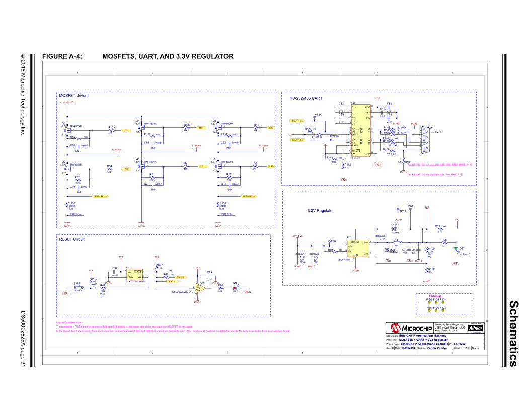
URE A-4: MOSFETS, UART, AND 3.3V REGULATOR
1
1
2
2
3
3
4
4
U_Motor
W_Motor
PGND
3V3
1kR139
10kR120
C2-19
DZ14
DY15
Z7
VCC18
C1+1
C1-2
C2+20
ISL3330
Y6
VS-11
VS+3
B5
RA17
RB16
A4
485/2328
GND10
DEN9
ON13
RXEN12
U8
3V3
TP15
TP16UART_Rx
UART_Tx
HS0HS2
LS0LS2
1 2
EG4576
SW2
100R06031%
R69
3V3
10k06031%
R70 GND1
RESET2
MR3
Vcc4
MIC6315-26D2UY
U4
3V3 3V3
2 4VCC
5
GND
3
VCC
GNDD
C
D
U5
74LVC1G14GW,125
3V3
RST#
RED
D9
RESET Circuit
2.2k
R80
4.7kR78
RS-232/485 UART
IPHASEA+ IPHASEB+
V_Motor
HS1
LS1
47R
R127
47R
R2
300kR126
5600pF
DNP
C86
5600pF
DNP
C2
47R
R128
47R
R34
300kR15
5600pF
DNP
C10
5600pF
DNP
C19
47R
R41
47R
R56
300kR132
5600pF
DNP
C92
5600pF
DNP
C34
PGND PGND
0.025R2512
R1300.025R2512
R133
MOSFET drivers
0R
DNP
R141
0RR140
/MCLR470R
DNP
R66
IPHASEA-
24V_MOTOR
0.1uF
C83
0.1uF
C85
0.1uF
C97
0.1uF
C99
DGND
DGND
DGND
DGNDDGND
DGND
IPHASEB-
There must be a PCB trace that connects R46 and R49 directly to the lower side of the two shunts on MOSFET driver circuit.In the layout, two traces coming from each shunt and connecting to R39-R46 and R40-R46 should run parallel to each other, as close as possible to each other and as far away as possible from any switching signal.
Layout Considerations -
300k
R31300k
R1
300k
R57
24V_SYS
3.3V Regulator
TP6
DGND
DGND
0RR101
BOOST
1
GND
2
VFB3
EN4
SW6
VIN5
BOOST
GND VFBEN
SWVIN
MCP16301HT
U7
4.7uF50V0805
C75
DGND
4.7uF50V0805
C76
4
1,2,3
5,6,7,8 TPHR8504PLQ1
4
1,2,3
5,6,7,8 TPHR8504PLQ5
4
1,2,3
5,6,7,8 TPHR8504PLQ2
4
1,2,3
5,6,7,8 TPHR8504PLQ4
4
1,2,3
5,6,7,8 TPHR8504PLQ6
4
1,2,3
5,6,7,8 TPHR8504PLQ3
Eth
erCA
T P
®, U
AR
T, an
d M
oto
r Co
ntro
l Ap
plic
ation
Exam
ple
DS
50002825A
-page 32
2018 M
icrochip Technolo
gy Inc.
5
5
6
6
D
C
B
A
Page Title:
Project Name:
EtherCAT P Connector + MagenticsEtherCAT P Applications Example PN: LAN9252
Description:
Date:Size: Sheet of RevB 5 5 D10/26/2018 Designer: Parthiv Pandya
EtherCAT P Applications Example
Designed withMicrochip Technology, Inc.USB/Network Group - UNGwww.Microchip.com
Altium.com
Earth
Earth
0 ("IN")
F
1M06031%
R97
10000pF
C69
24V_MOTOR
UpGND
ernal supply (Up) on TP3/TP4
GND
UsGND
UpGND Earth
GND
10000pF
C24
24V_MOTOR
CAT-P
FIGURE A-5: ETHERCAT P® CONNECTORS AND MAGNETICS
1
1
2
2
3
3
4
4
D
C
B
AVDD33TXRX1
0.022uF50V
C71
L2 L2'
L1 L1'
CM Choke 90Ohm
L9
L2 L2'
L1 L1'
CM Choke 90Ohm
L7
75R06031%
R13775R06031%
R138
VDD33TXRX2
0.022uF
C37
L2 L2'
L1 L1'
CM Choke 90Ohm
L4
L2 L2'
L1 L1'
CM Choke 90Ohm
L5
75R
R61
75R
R62
1uF
C62
1uF
C63
1uF
C56
1uF
C57
24V_SYS
49.9RR72
49.9RR67
49.9RR83
49.9RR81
49.9RR92
49.9RR95
49.9RR86
49.9RR88
0RR65
0RR99
1uF
C41
1uF
C38
1uF
C48
1uF
C45
Earth
Earth
PORT 1 ("OUT")
PORT
EtherCAT P - PORT 0
EtherCAT P - PORT 124V DC power OUT (for power forwarding)
1M06031%
R134
10000p
C93
10pFC64
10pFC67
10pFC58
10pFC59
10pFC42
10pFC39
10pFC54
10pFC51
10uFC70
10uF50V
C55
TXA_N
TXA_P
RXA_N
RXA_P
TXB_N
TXB_P
RXB_N
RXB_P
T4_P
T4_N
T3_P
T3_N
L8_P
L8_N
L7_P
L7_N
T1_P
T1_N
T2_P
T2_N
L5_P
L5_N
L6_P
L6_N
0R
R91
0R
R94
0R
R87
0R
R89
0R
R79
0R
R77
0R
R85
0R
R84
D19
D16
D12
D13
L8'_P
L8'_N
L7'_P
L7'_N
J2TX_P
J2TX_N
J2RX_P
J2RX_N
L5'_P
L5'_N
L6'_P
L6'_N
J1TX_P
J1TX_N
J1RX_P
J1RX_N
TP4
24V DC External supply (Us) on TP1/TP2 TP5
TP3
24V DC Ext
DGND
DGND
DGND
D
UsGND
10uFC98
24V_SYS
UsGND
DGND
P
10uF50V
C50TP1
TP2
UpGNDPGND
10000pF
C25
DGND
DGND
DGND
DGND
D17
D18
D14
D15
D8
D7
6
2
51
*
* *
3
4
*
ALT4532M
TR4
6
2
51
*
* *
3
4
*
ALT4532M
TR3
6
2
51
*
* *
3
4*ALT4532M
TR1
6
2
51
*
* *
3
4*ALT4532M
TR2
6.8uH
L66.8uH
L8
6.8uH
L126.8uH
L13
6.8uH
L116.8uH
L10
6.8uH
L26.8uH
L3
0R0805
R82
D11
D10
1000pF2KV
C73
1000pF2KV
C77
12
34RX
+
TX+
TX-
RX-
SH
EtherCAT-PJ5
12
34RX
+
TX+
TX-
RX-
SH
EtherJ7
2018 Microchip Technology Inc. DS50002825A-page 33
NOTES:
DS50002825A-page 34 2018 Microchip Technology Inc.
AMERICASCorporate Office2355 West Chandler Blvd.Chandler, AZ 85224-6199Tel: 480-792-7200 Fax: 480-792-7277Technical Support: http://www.microchip.com/supportWeb Address: www.microchip.com
AtlantaDuluth, GA Tel: 678-957-9614 Fax: 678-957-1455
Austin, TXTel: 512-257-3370
BostonWestborough, MA Tel: 774-760-0087 Fax: 774-760-0088
ChicagoItasca, IL Tel: 630-285-0071 Fax: 630-285-0075
DallasAddison, TX Tel: 972-818-7423 Fax: 972-818-2924
DetroitNovi, MI Tel: 248-848-4000
Houston, TX Tel: 281-894-5983
IndianapolisNoblesville, IN Tel: 317-773-8323Fax: 317-773-5453Tel: 317-536-2380
Los AngelesMission Viejo, CA Tel: 949-462-9523Fax: 949-462-9608Tel: 951-273-7800
Raleigh, NC Tel: 919-844-7510
New York, NY Tel: 631-435-6000
San Jose, CA Tel: 408-735-9110Tel: 408-436-4270
Canada - TorontoTel: 905-695-1980 Fax: 905-695-2078
ASIA/PACIFICAustralia - SydneyTel: 61-2-9868-6733
China - BeijingTel: 86-10-8569-7000
China - ChengduTel: 86-28-8665-5511
China - ChongqingTel: 86-23-8980-9588
China - DongguanTel: 86-769-8702-9880
China - GuangzhouTel: 86-20-8755-8029
China - HangzhouTel: 86-571-8792-8115
China - Hong Kong SARTel: 852-2943-5100
China - NanjingTel: 86-25-8473-2460
China - QingdaoTel: 86-532-8502-7355
China - ShanghaiTel: 86-21-3326-8000
China - ShenyangTel: 86-24-2334-2829
China - ShenzhenTel: 86-755-8864-2200
China - SuzhouTel: 86-186-6233-1526
China - WuhanTel: 86-27-5980-5300
China - XianTel: 86-29-8833-7252
China - XiamenTel: 86-592-2388138
China - ZhuhaiTel: 86-756-3210040
ASIA/PACIFICIndia - BangaloreTel: 91-80-3090-4444
India - New DelhiTel: 91-11-4160-8631
India - PuneTel: 91-20-4121-0141
Japan - OsakaTel: 81-6-6152-7160
Japan - TokyoTel: 81-3-6880- 3770
Korea - DaeguTel: 82-53-744-4301
Korea - SeoulTel: 82-2-554-7200
Malaysia - Kuala LumpurTel: 60-3-7651-7906
Malaysia - PenangTel: 60-4-227-8870
Philippines - ManilaTel: 63-2-634-9065
SingaporeTel: 65-6334-8870
Taiwan - Hsin ChuTel: 886-3-577-8366
Taiwan - KaohsiungTel: 886-7-213-7830
Taiwan - TaipeiTel: 886-2-2508-8600
Thailand - BangkokTel: 66-2-694-1351
Vietnam - Ho Chi MinhTel: 84-28-5448-2100
EUROPEAustria - WelsTel: 43-7242-2244-39Fax: 43-7242-2244-393
Denmark - CopenhagenTel: 45-4450-2828 Fax: 45-4485-2829
Finland - EspooTel: 358-9-4520-820
France - ParisTel: 33-1-69-53-63-20 Fax: 33-1-69-30-90-79
Germany - GarchingTel: 49-8931-9700
Germany - HaanTel: 49-2129-3766400
Germany - HeilbronnTel: 49-7131-67-3636
Germany - KarlsruheTel: 49-721-625370
Germany - MunichTel: 49-89-627-144-0 Fax: 49-89-627-144-44
Germany - RosenheimTel: 49-8031-354-560
Israel - Ra’anana Tel: 972-9-744-7705
Italy - Milan Tel: 39-0331-742611 Fax: 39-0331-466781
Italy - PadovaTel: 39-049-7625286
Netherlands - DrunenTel: 31-416-690399 Fax: 31-416-690340
Norway - TrondheimTel: 47-7288-4388
Poland - WarsawTel: 48-22-3325737
Romania - BucharestTel: 40-21-407-87-50
Spain - MadridTel: 34-91-708-08-90Fax: 34-91-708-08-91
Sweden - GothenbergTel: 46-31-704-60-40
Sweden - StockholmTel: 46-8-5090-4654
UK - WokinghamTel: 44-118-921-5800Fax: 44-118-921-5820
Worldwide Sales and Service
08/15/18