evolution of ev charging and solutions for future needs
TRANSCRIPT

TI Information – Selective Disclosure
Evolution of EV charging and solutions for future needs
by Harald Parzhuber
1
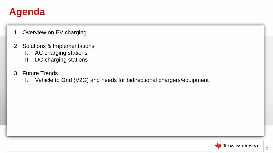
1. Overview on EV charging
2. Solutions & Implementations
I. AC charging stations
II. DC charging stations
3. Future Trends
I. Vehicle to Grid (V2G) and needs for bidirectional chargers/equipment
2
Agenda
TI Information – Selective Disclosure
Overview of EV charging
1. Overview on EV charging
2. Solutions & Implementations
• AC charging stations
• DC charging stations
3. Future Trends
• Vehicle to Grid (V2G) and needs for bidirectional chargers/equipment
3
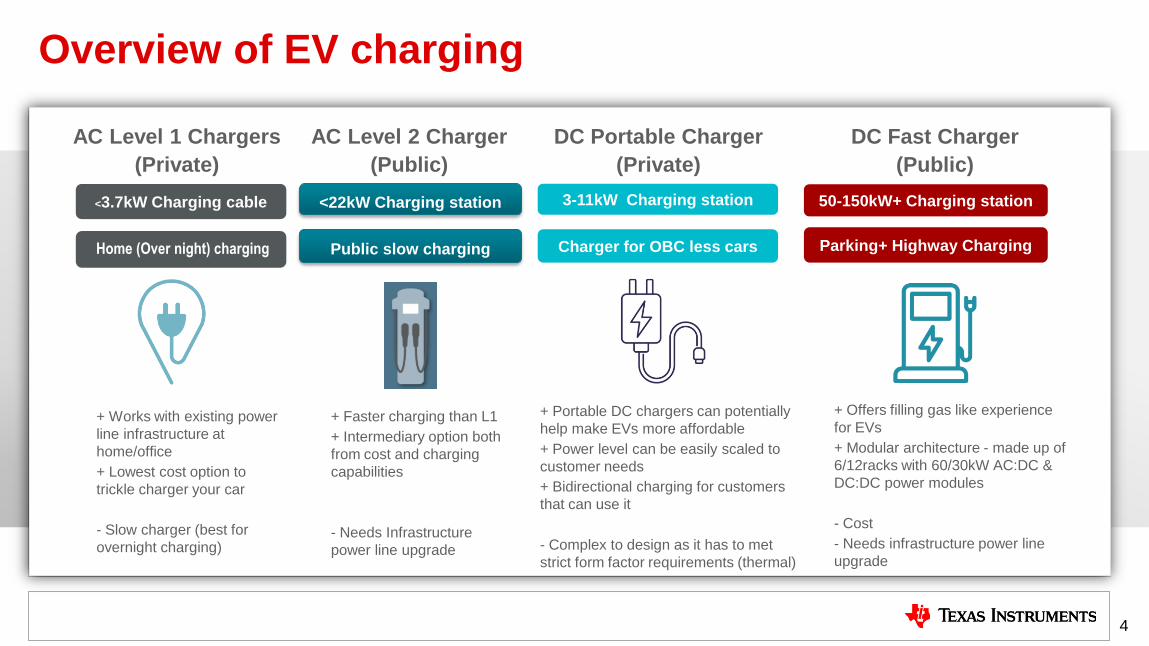
<3.7kW Charging cable
Public slow charging
<22kW Charging station 20%-50% savings20-80KW
Micro
Inverter
Power
Optimizer
+ Works with existing power
line infrastructure at
home/office
+ Lowest cost option to
trickle charger your car
- Slow charger (best for
overnight charging)
Home (Over night) charging
20%-50% savings
20-80KW
Parking+ Highway Charging
50-150kW+ Charging station
+ Faster charging than L1
+ Intermediary option both
from cost and charging
capabilities
- Needs Infrastructure
power line upgrade
+ Portable DC chargers can potentially
help make EVs more affordable
+ Power level can be easily scaled to
customer needs
+ Bidirectional charging for customers
that can use it
- Complex to design as it has to met
strict form factor requirements (thermal)
+ Offers filling gas like experience
for EVs
+ Modular architecture - made up of
6/12racks with 60/30kW AC:DC &
DC:DC power modules
- Cost
- Needs infrastructure power line
upgrade
AC Level 1 Chargers
(Private)
AC Level 2 Charger
(Public)
DC Fast Charger
(Public)
DC Portable Charger
(Private)
3-11kW Charging station
Charger for OBC less cars
4
Overview of EV charging
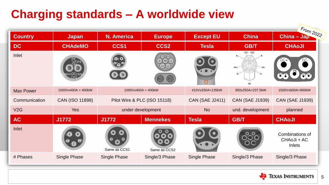
Charging standards – A worldwide view
Country Japan N. America Europe Except EU China China – Jap
DC CHAdeMO CCS1 CCS2 Tesla GB/T CHAoJI
Inlet
Max Power 1000Vx400A = 400kW 1000Vx400A = 400kW 410Vx330A=135kW 950x250A=237.5kW 1500Vx600A=900kW
Communication CAN (ISO 11898) Pilot Wire & PLC (ISO 15118) CAN (SAE J2411) CAN (SAE J1939) CAN (SAE J1939)
V2G Yes under development No und. development planned
AC J1772 J1772 Mennekes Tesla GB/T CHAoJI
Inlet
Combinations of
CHAoJi + AC
Inlets
# Phases Single Phase Single Phase Single/3 Phase Single Phase Single/3 Phase Single/3 Phase
5
DC + DC -
L1L2/N
CP PPPE
DC + DC -
PE
CAN-H CAN-L
CP1CP3
CP2
CP
L2
L1
L3
N
CC
PEL1L2/N
CP PPPE
Same as CCS2Same as CCS1
TI Information – Selective Disclosure
Charging solutions – AC charging
1. Overview on EV charging
2. Solutions & Implementations
• AC charging stations
• DC charging stations
3. Future Trends
• Vehicle to Grid (V2G) and needs for bidirectional chargers/equipment
6
Level 1 & 2 EV charging station
IO
Voltages
AC Grid Connection Vehicle Connection
Input Power Protection
E-Fuse
Isolated AC/DC Power
Supply
Isolated
AC/DC
Non-Isolated DC/DC
Power Supply
Low Noise Power
DC/DC
Isolated DC/DC
Power Supply
Isolated
DC/DC
Isolated
Power
Wired
Interface
Pilot Wire
PLC
RS-232
RS-485
Signal Input/
Output
Protection
ESD
Signal
Isolation
Data
Isolation
Wireless
Interface
NFC
Wi-Fi
Clocking
RTC
Analog Front End
ADC Reference
Relay Control
Power Stage
Relay
Driver
Relay
Input Current and
Voltage Sense
AMP
ISO
AMP
Current Sensor
Input Current and
Voltage Sense
AMP
ISO
AMP
Current Sensor
Output User
Interface
LED
Driver
LCD
Display
Digital Processing
MCU/MPUPWM
Controller
SVS RTC
TIDA-00637
Gen-1
J1772 compliant L1/2 EVSE
TIDC-EVSE-WIFI
WiFi® enabled L1/2 EVSE
TIDC-EVSE-NFC
NFC enabled L1/2 EVSE
TIDA-010071
Gen-2
J1772 compliant L1/2 EVSE
7
• SAE J1772 compliant pilot signal output and return
• High efficiency, tight output voltage regulated, low standby isolated
AC-DC fly back power stage based on UCC28740 and TL431
• DRV110 current controller used for driving high current relays or
contactors
• Isolated line voltage sensing using ISO1212 digital-input receiver for
welded relay/contactor detection
• Onboard Launchpad connectors to interface with any MCU family
• Output voltage regulation (<±5% ) of AC-DC flyback stage and high
slew of TL1805 enables to meet SAE J1772 certification for control
pilot interface
• Low standby of UCC28740 based AC-DC stage enables to achieve
energy star ratings for EV charging stations
• Current controlled relay/contactor driver to avoid thermal problems and
reduce power dissipation
• Isolated line voltage sensing to detect fusing of contacts due to arcing
Features
Benefits
• TIDA-010071
• Design Files: Schematics, BOM and BOM Analysis, CAD Files
• Key TI Devices: UCC28740, TL431 DRV110, ISO1212,
TLV1805, CSD19538Q5A
Level 1 and 2 SAE J1772 compliant EV Service Equipment (EVSE) – Reference design TIDA-010071
8
Tools & Resources
• AC charging (pile) station
• DC charging (pile) station
Applications

System block diagram
9
TIDA-010071 Block Diagram
EVSE GND
1
2
3
4
5Monitoring circuit
Line
Neutral
J1772 Charge Coupler
Electric Vehicle Inlet
UCC28740Constant-Voltage Constant-Current
Flyback
TLV713P150mA LDO with Foldback Current
Limit
+12V
-12V
+5V
Enable
ISO1212Isolated 24-V to 60-V digital input receiver
Drive
Pilot Control
OUT1
OUT2
+12V
-12V
TLV1805µ-Power
+3.3V
+5V
+3.3V
+12V+12V
+3.3V
Relay/Contactor
DRV110Single-Channel Relay Low-Side
Controller CSD19534Q5A
TI Launchpad
AC PowerGNDDC InputDC OutputLogic SignalsIsolation
TL431 Precision
Programmable Reference
Feedback
40% reduction in power dissipation using DRV110
10
Features:
• DRV110 capable of driving any solenoid with
extended period of actuation of solenoids, relays,
contactors, etc
• Reliable ON/OFF through current control
• Peak/hold current architecture
• Internal Zener and external FET support high-
voltage VIN:
o 120V and 230V AC supply through rectifier and
RS resistor
o 24V, 48V, and higher DC supply through RS
resistor
Benefits:
• Reliable current control ensures relays stay
energized regardless of temperature
• Peak/hold current architecture reduces power
consumption (Half as compared to constant
voltage drive) and thermal dissipation resulting in
higher performance efficiency over time
• Integrated Zener can accommodate a wide range of
voltages, external FET can be sized for suitable
current
Constant Voltage Drive
Average Power = 944mWDRV110 based Current Drive
Average Power = 535mW
Relay or
Contactor
Gate PWM ON
Hold Current

SAE J1772 compliant control pilot signal interface
11
Pilot signal rise time = 42ns
Pilot signal fall time = 95ns

Isolated line sensing for contact weld detection
12
• For safety reasons, detecting the output
voltage of the primary relay is critical
• The contacts can experience arcing and
become fused together, providing power
to the plug even when the system is not
powering it
• Checking that the operation completed
correctly is important and should be done
every time the relay is opened
• To implement this check, the ISO1212
fully-integrated, isolated digital-input
receiver is used to sense line voltage
• The outputs (OUT1 and OUT2) from the
ISO1212 device are GPIO-level DC
signals that are high when voltage is
present and are fed directly into the MCU
for fault detection
TI Information – Selective Disclosure
DC charging stations
1. Overview on EV charging
2. Solutions & Implementations
• AC charging stations
• DC charging stations
3. Future Trends
• Vehicle to Grid (V2G) and needs for bidirectional chargers/equipment
13
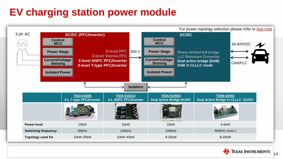
EV charging station power module
14
AC/DC (PFC/Inverter)
2-level PFC
3-level Vienna PFC
3-level ANPC PFC/Inverter
3-level T-type PFC/Inverter
ControlMCU
Isolated Power
Power Stage
DC/DC
Phase shifted full bridge
LLC Resonant Converter
Dual active bridge (DAB)
DAB in CLLLC mode
Isolation
800 V
50-920VDC
3 ph AC
CAN/PLCCurrent/Voltage
Sensing
For power topology selection please refer to App note
ControlMCU
Isolated Power
Power Stage
Current/Voltage Sensing
TIDA-01606
3-L T-type PFC/Inverter
TIDA-010210
3-L ANPC PFC/Inverter
TIDA-010054
Dual Active Bridge DC/DC
TIDM-02002
Dual Active Bridge in CLLLC DC/DC
Power level 10kW 10kW 10kW 6.6kW
Switching frequency 50kHz 100kHz 100kHz 500kHz (nom.)
Topology used for 10kW-25kW 10kW-40kW 8-25kW 8-25kW
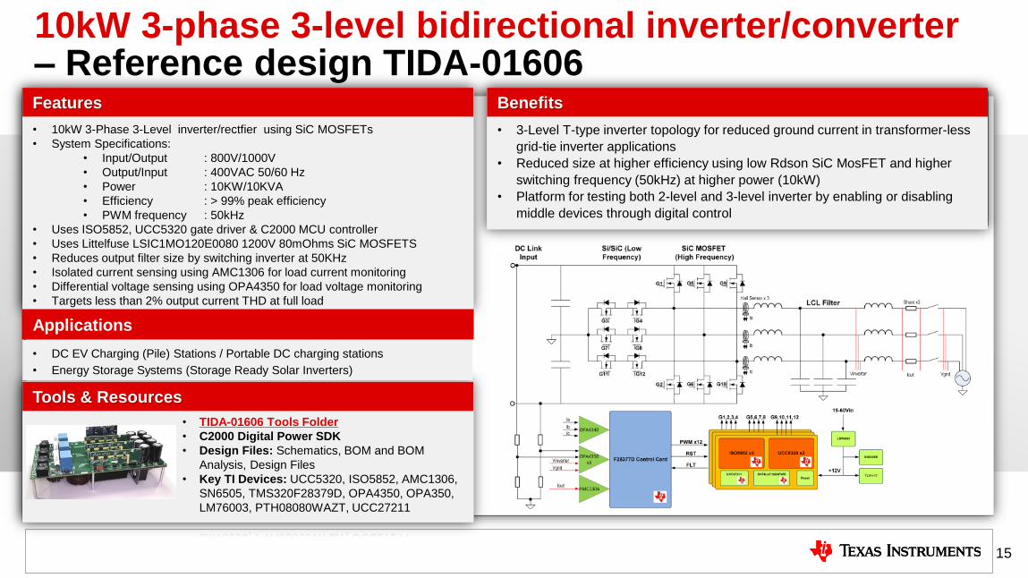
• 10kW 3-Phase 3-Level inverter/rectfier using SiC MOSFETs
• System Specifications:
• Input/Output : 800V/1000V
• Output/Input : 400VAC 50/60 Hz
• Power : 10KW/10KVA
• Efficiency : > 99% peak efficiency
• PWM frequency : 50kHz
• Uses ISO5852, UCC5320 gate driver & C2000 MCU controller
• Uses Littelfuse LSIC1MO120E0080 1200V 80mOhms SiC MOSFETS
• Reduces output filter size by switching inverter at 50KHz
• Isolated current sensing using AMC1306 for load current monitoring
• Differential voltage sensing using OPA4350 for load voltage monitoring
• Targets less than 2% output current THD at full load
• 3-Level T-type inverter topology for reduced ground current in transformer-less
grid-tie inverter applications
• Reduced size at higher efficiency using low Rdson SiC MosFET and higher
switching frequency (50kHz) at higher power (10kW)
• Platform for testing both 2-level and 3-level inverter by enabling or disabling
middle devices through digital control
Features Benefits
• TIDA-01606 Tools Folder
• C2000 Digital Power SDK
• Design Files: Schematics, BOM and BOM
Analysis, Design Files
• Key TI Devices: UCC5320, ISO5852, AMC1306,
SN6505, TMS320F28379D, OPA4350, OPA350,
LM76003, PTH08080WAZT, UCC27211
10kW 3-phase 3-level bidirectional inverter/converter – Reference design TIDA-01606
15
Tools & Resources
• DC EV Charging (Pile) Stations / Portable DC charging stations
• Energy Storage Systems (Storage Ready Solar Inverters)
Applications
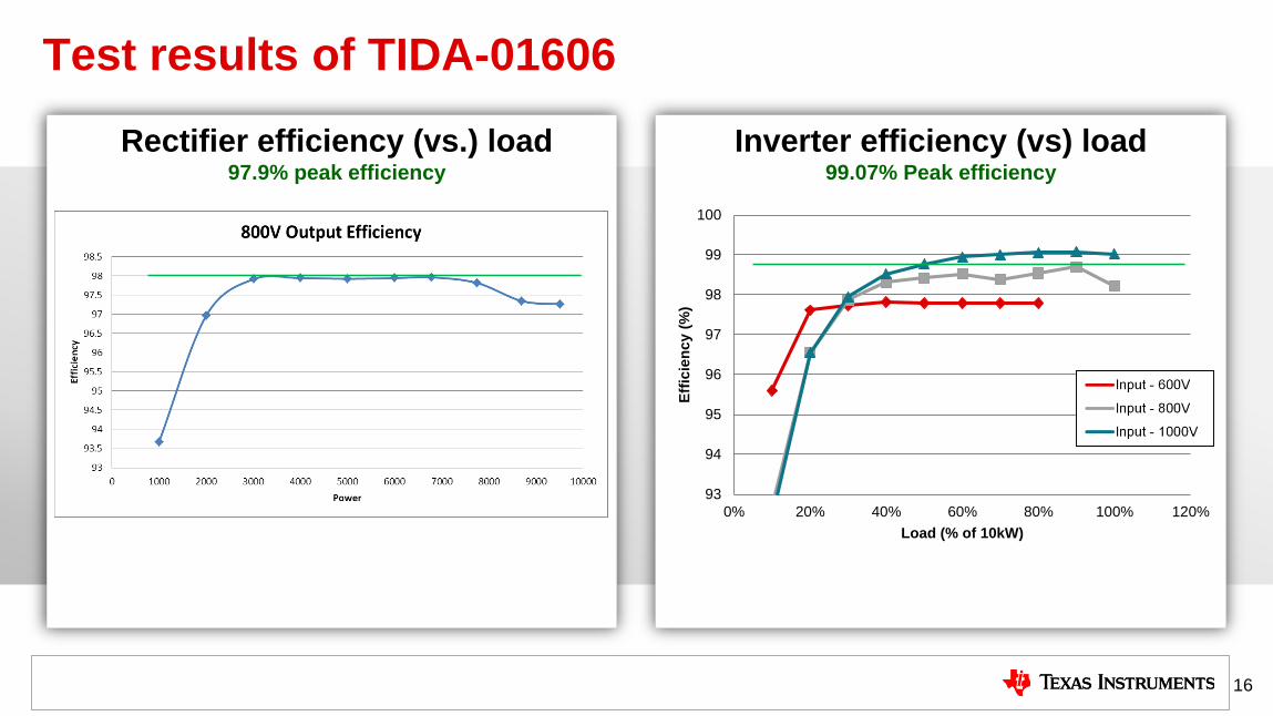
Test results of TIDA-01606
16
Inverter efficiency (vs) load99.07% Peak efficiency
93
94
95
96
97
98
99
100
0% 20% 40% 60% 80% 100% 120%
Eff
icie
ncy (
%)
Load (% of 10kW)
Rectifier efficiency (vs.) load97.9% peak efficiency
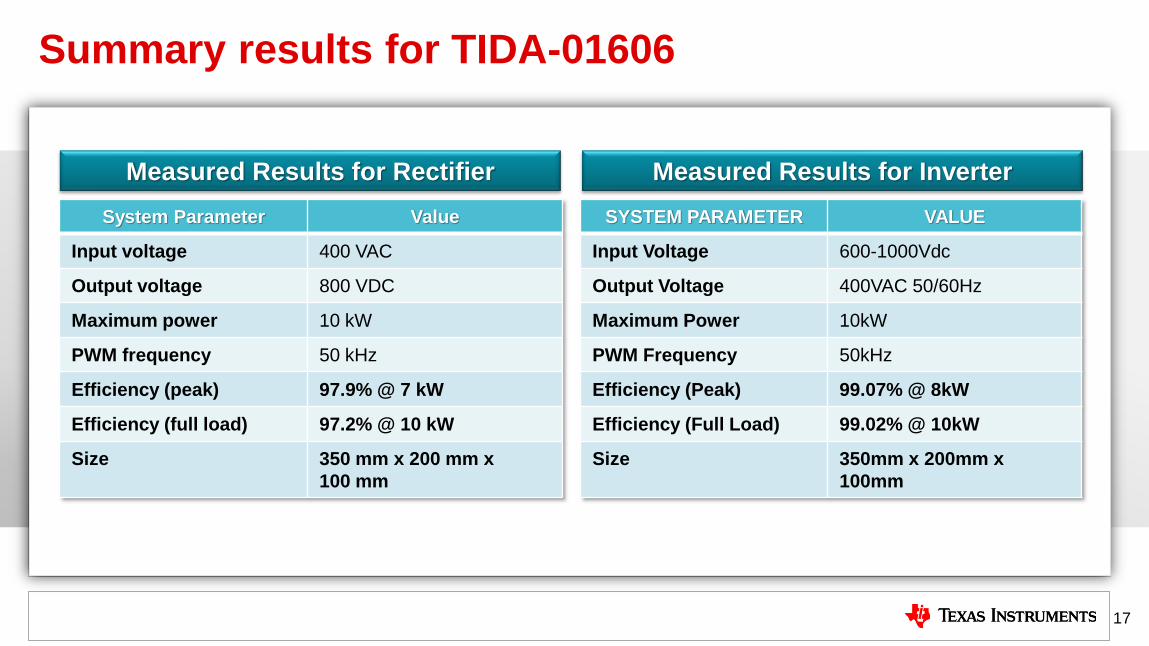
SYSTEM PARAMETER VALUE
Input Voltage 600-1000Vdc
Output Voltage 400VAC 50/60Hz
Maximum Power 10kW
PWM Frequency 50kHz
Efficiency (Peak) 99.07% @ 8kW
Efficiency (Full Load) 99.02% @ 10kW
Size 350mm x 200mm x
100mm
Measured Results for Inverter
Summary results for TIDA-01606
17
System Parameter Value
Input voltage 400 VAC
Output voltage 800 VDC
Maximum power 10 kW
PWM frequency 50 kHz
Efficiency (peak) 97.9% @ 7 kW
Efficiency (full load) 97.2% @ 10 kW
Size 350 mm x 200 mm x
100 mm
Measured Results for Rectifier
• DC EV Charging (Pile) Stations / Portable DC charging stations
• Energy Storage Systems (Storage Ready Solar Inverters)
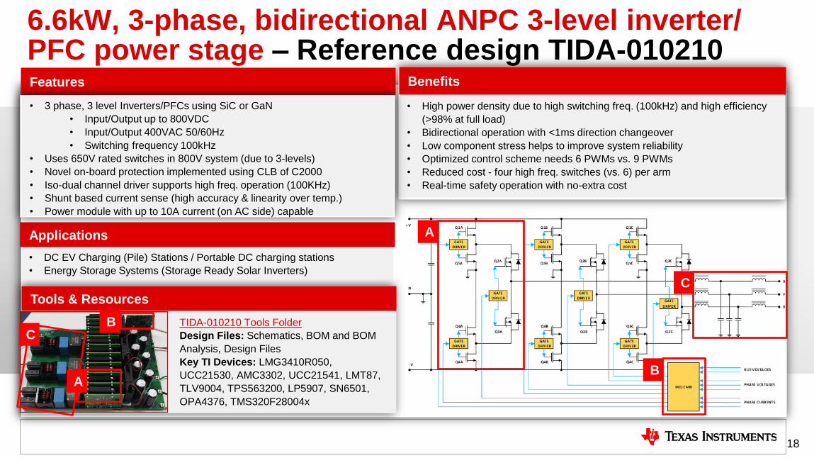
• High power density due to high switching freq. (100kHz) and high efficiency
(>98% at full load)
• Bidirectional operation with <1ms direction changeover
• Low component stress helps to improve system reliability
• Optimized control scheme needs 6 PWMs vs. 9 PWMs
• Reduced cost - four high freq. switches (vs. 6) per arm
• Real-time safety operation with no-extra cost
• TIDA-010210 Tools Folder
• Design Files: Schematics, BOM and BOM
Analysis, Design Files
• Key TI Devices: LMG3410R050,
UCC21530, AMC3302, UCC21541, LMT87,
TLV9004, TPS563200, LP5907, SN6501,
OPA4376, TMS320F28004x
6.6kW, 3-phase, bidirectional ANPC 3-level inverter/ PFC power stage – Reference design TIDA-010210
18
BenefitsFeatures
Applications
• 3 phase, 3 level Inverters/PFCs using SiC or GaN
• Input/Output up to 800VDC
• Input/Output 400VAC 50/60Hz
• Switching frequency 100kHz
• Uses 650V rated switches in 800V system (due to 3-levels)
• Novel on-board protection implemented using CLB of C2000
• Iso-dual channel driver supports high freq. operation (100KHz)
• Shunt based current sense (high accuracy & linearity over temp.)
• Power module with up to 10A current (on AC side) capable
Tools & Resources
A
AB
B
C
C
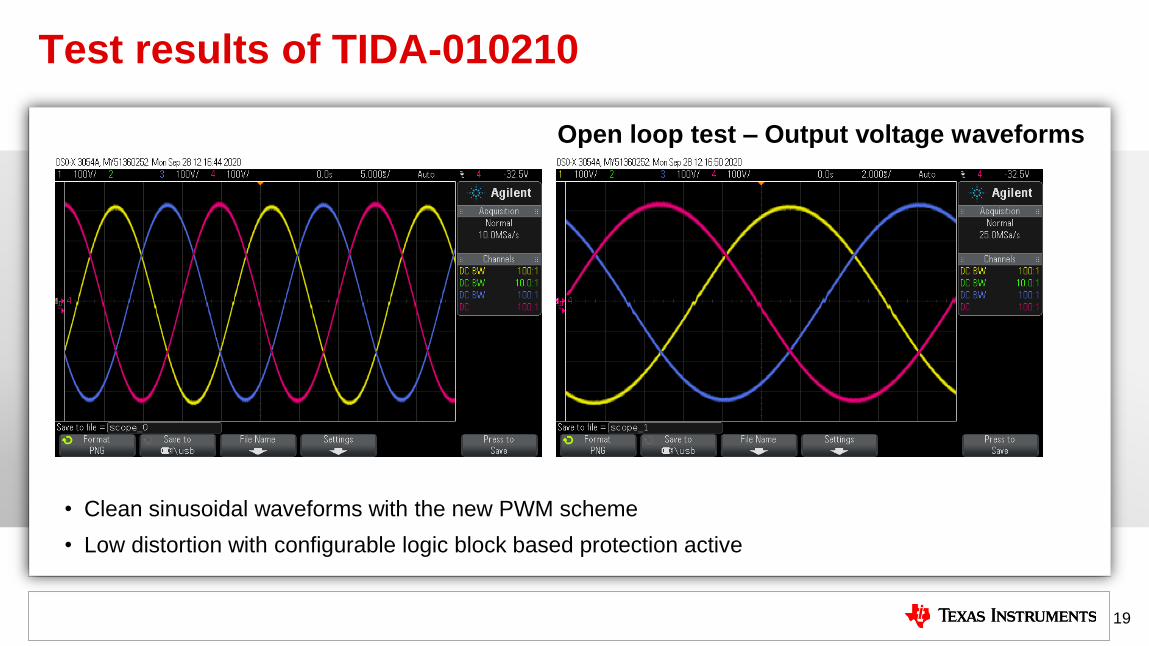
Test results of TIDA-010210
19
Open loop test – Output voltage waveforms
• Clean sinusoidal waveforms with the new PWM scheme
• Low distortion with configurable logic block based protection active
Transient response
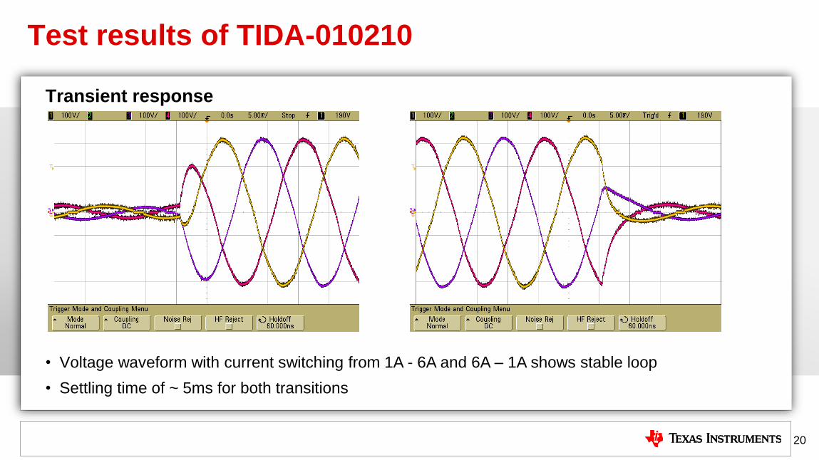
Test results of TIDA-010210
20
• Voltage waveform with current switching from 1A - 6A and 6A – 1A shows stable loop
• Settling time of ~ 5ms for both transitions
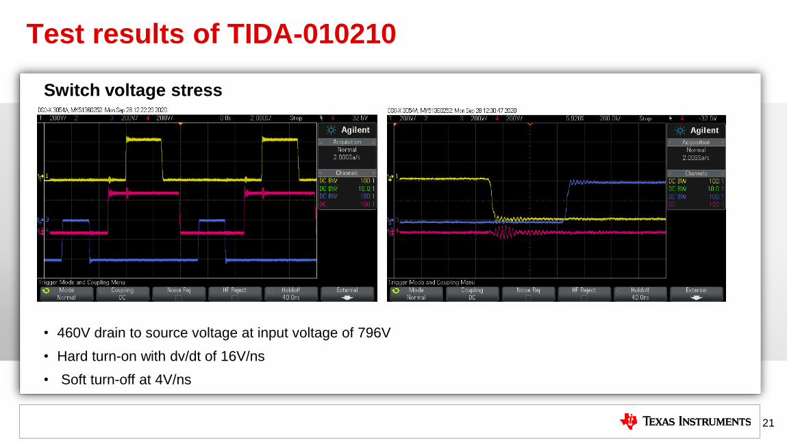
Switch voltage stress
• 460V drain to source voltage at input voltage of 796V
• Hard turn-on with dv/dt of 16V/ns
• Soft turn-off at 4V/ns
Test results of TIDA-010210
21
Test results of TIDA-010210
22
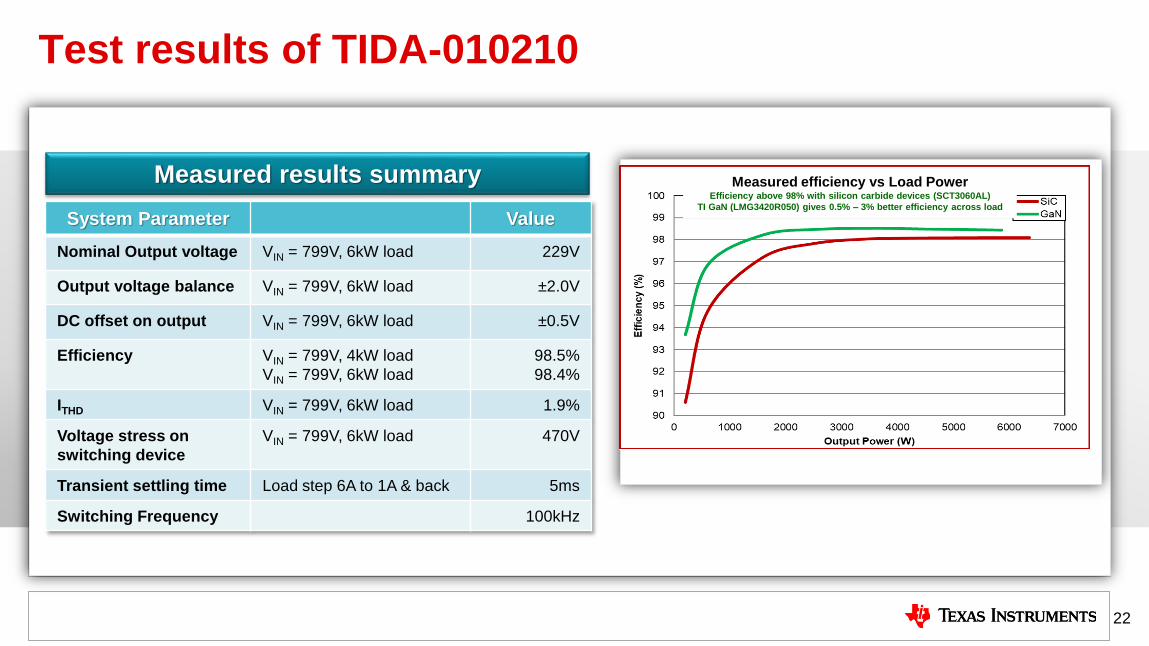
System Parameter Value
Nominal Output voltage VIN = 799V, 6kW load 229V
Output voltage balance VIN = 799V, 6kW load ±2.0V
DC offset on output VIN = 799V, 6kW load ±0.5V
Efficiency VIN = 799V, 4kW load
VIN = 799V, 6kW load
98.5%
98.4%
ITHD VIN = 799V, 6kW load 1.9%
Voltage stress on
switching device
VIN = 799V, 6kW load 470V
Transient settling time Load step 6A to 1A & back 5ms
Switching Frequency 100kHz
Measured results summary Measured efficiency vs Load PowerEfficiency above 98% with silicon carbide devices (SCT3060AL)
TI GaN (LMG3420R050) gives 0.5% – 3% better efficiency across load

• DC Charging (Pile) Station / Portable DC Charging Station
• On board chargers (OBC)
• Power conversion systems (PCS) in energy storage
Bidirectional Dual Active Bridge (DAB) DC/DC – Reference design TIDA-010054
23
• Input Voltage: 700-800-V DC (HV-Bus voltage/Vienna output)
• Output Voltage: 350-500 V
• Output power level: 10kW (@400 – 500V) , 7.5KW (@350V)
• Single phase DAB capable of bidirectional operation
• Soft switching operation of switches over a wide range
• Achieves peak efficiency – 98.2%, full load efficiency – 97.5%
• Less than 3% ripple target for output voltage
• Dual channel reinforced isolated gate driver
• Single phase shift modulation
• Switching frequency -100 kHz
• Power density – 2.25 KW/L
Features
Applications
Tools & Resources
• TIDA-010054 Tools Folder
• Design Files: Schematics, BOM and BOM
Analysis, Design Files
• Key TI Devices: TMS320F280049, AMC1311,
AMC3302, AMC3306 UCC21530, ISO7721,
TPS82130, SN6501, SN6505, OPA320
• Single phase shift modulation provides easy control loop implementation.
Can be extended to dual phase shift modulation for better range of ZVS
and efficiency
• SiC devices offer best in class power density and efficiency
• Dual channel reinforced gate driver UCC21530 reduces the total
component count for driving SiC MOSFETS
• Provides modularity and ease of bidirectional operation
Benefits
Test results of TIDA-010054
24
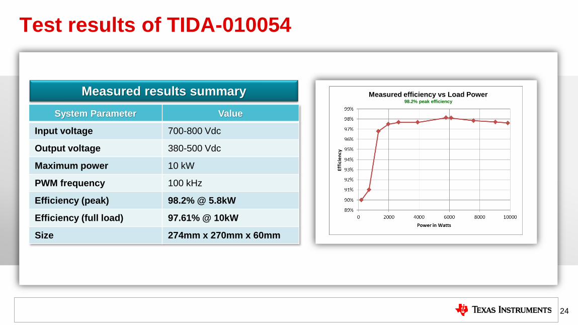
System Parameter Value
Input voltage 700-800 Vdc
Output voltage 380-500 Vdc
Maximum power 10 kW
PWM frequency 100 kHz
Efficiency (peak) 98.2% @ 5.8kW
Efficiency (full load) 97.61% @ 10kW
Size 274mm x 270mm x 60mm
Measured results summary Measured efficiency vs Load Power98.2% peak efficiency
• On Board Chargers (OBC)
• DC Charing (Pile) Station / Portable DC Chargers
• Power conversion systems (PCS) in energy storage
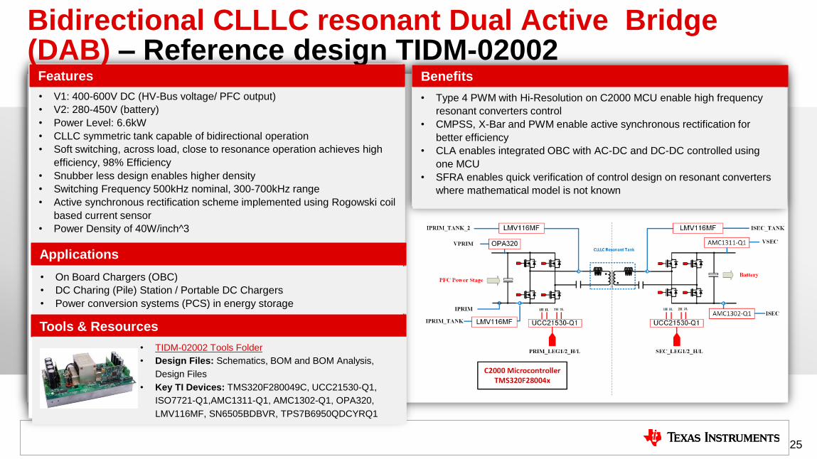
Bidirectional CLLLC resonant Dual Active Bridge (DAB) – Reference design TIDM-02002
25
• Type 4 PWM with Hi-Resolution on C2000 MCU enable high frequency
resonant converters control
• CMPSS, X-Bar and PWM enable active synchronous rectification for
better efficiency
• CLA enables integrated OBC with AC-DC and DC-DC controlled using
one MCU
• SFRA enables quick verification of control design on resonant converters
where mathematical model is not known
• V1: 400-600V DC (HV-Bus voltage/ PFC output)
• V2: 280-450V (battery)
• Power Level: 6.6kW
• CLLC symmetric tank capable of bidirectional operation
• Soft switching, across load, close to resonance operation achieves high
efficiency, 98% Efficiency
• Snubber less design enables higher density
• Switching Frequency 500kHz nominal, 300-700kHz range
• Active synchronous rectification scheme implemented using Rogowski coil
based current sensor
• Power Density of 40W/inch^3
Features Benefits
Applications
Tools & Resources
• TIDM-02002 Tools Folder
• Design Files: Schematics, BOM and BOM Analysis,
Design Files
• Key TI Devices: TMS320F280049C, UCC21530-Q1,
ISO7721-Q1,AMC1311-Q1, AMC1302-Q1, OPA320,
LMV116MF, SN6505BDBVR, TPS7B6950QDCYRQ1
TI Information – Selective Disclosure
Future trends
1. Overview on EV charging
2. Solutions & Implementations
• AC charging stations
• DC charging stations
3. Future Trends
• Vehicle to Grid (V2G) and needs for bidirectional chargers/equipment
26
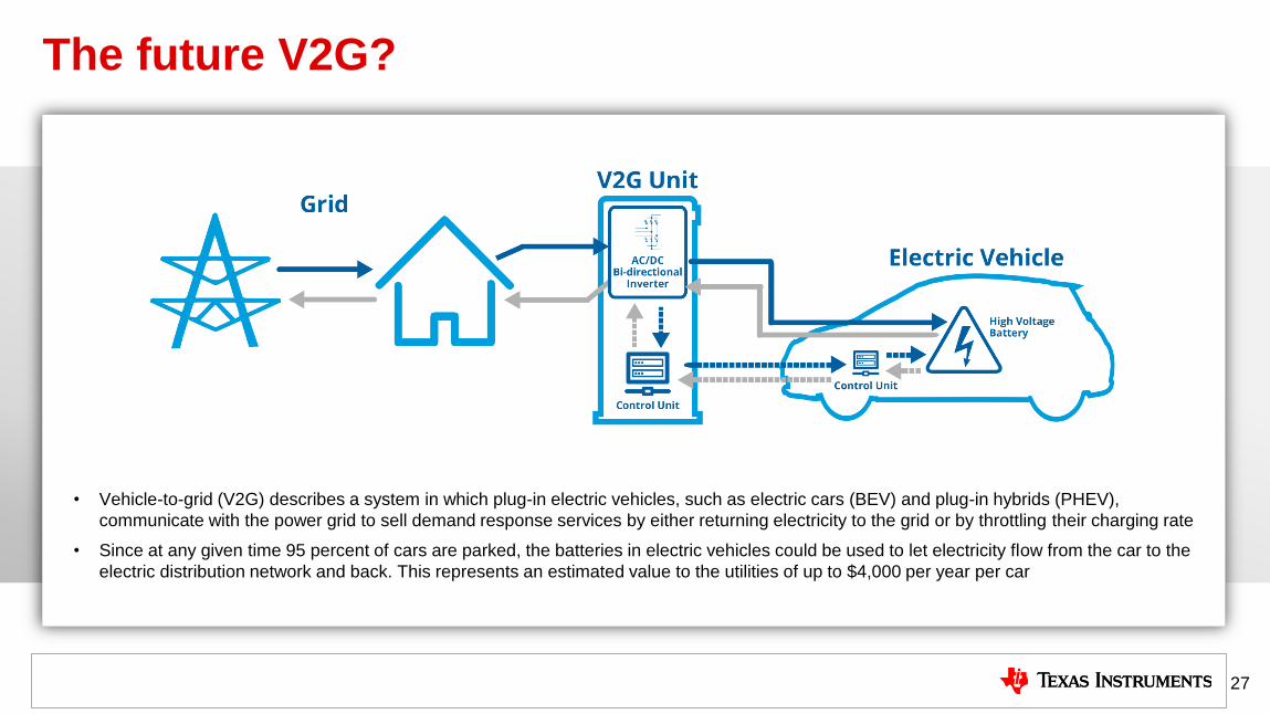
The future V2G?
• Vehicle-to-grid (V2G) describes a system in which plug-in electric vehicles, such as electric cars (BEV) and plug-in hybrids (PHEV),
communicate with the power grid to sell demand response services by either returning electricity to the grid or by throttling their charging rate
• Since at any given time 95 percent of cars are parked, the batteries in electric vehicles could be used to let electricity flow from the car to the
electric distribution network and back. This represents an estimated value to the utilities of up to $4,000 per year per car
27
Multilevel topologies enable vehicle to gird (V2G)
28
Multilevel topologies
• Smaller passives offer up to 50% reduction in size for a 3-level inverter vs. a 2-level inverter.
• Multilevel topology enables FETs with significantly lower switching and conduction losses which improves efficiency by using FETs
with half the blocking voltage for the same DC bus voltage
• Three level topologies keep the switching voltage to half of a 2-level inverter which improves overall EMI and makes EVs with 800V
battery technology easier to support
Bidirectional topologies
• GaN and SiC improve overall efficiency and absorbs losses in the additional switches required in a bidirectional topology
• Real-time micro controller with high-frequency PWMs and high-bandwidth current and voltage sensing enables that higher switching
frequency offered by GaN and SiC
• Bidirectional charging benefits customers with time-of-use plans and help make the grid more resilient
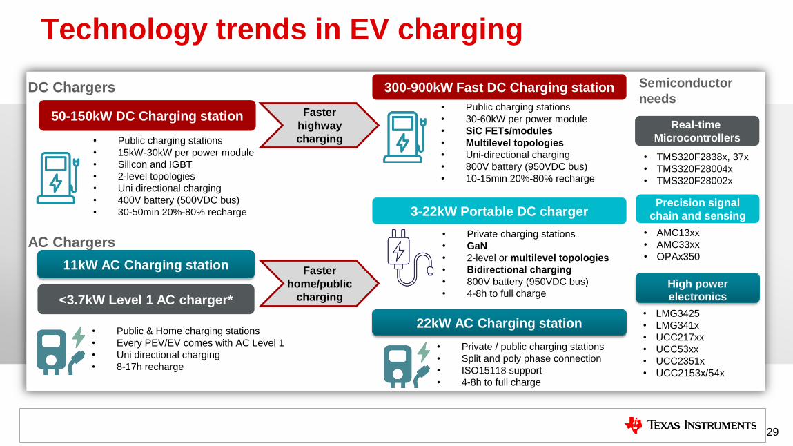
50-150kW DC Charging station
300-900kW Fast DC Charging station
• Public charging stations
• 30-60kW per power module
• SiC FETs/modules
• Multilevel topologies
• Uni-directional charging
• 800V battery (950VDC bus)
• 10-15min 20%-80% recharge
3-22kW Portable DC charger
• Public charging stations
• 15kW-30kW per power module
• Silicon and IGBT
• 2-level topologies
• Uni directional charging
• 400V battery (500VDC bus)
• 30-50min 20%-80% recharge
• Private charging stations
• GaN
• 2-level or multilevel topologies
• Bidirectional charging
• 800V battery (950VDC bus)
• 4-8h to full charge
Faster
highway
charging
Faster
home/public
charging<3.7kW Level 1 AC charger*
22kW AC Charging station
11kW AC Charging station
• Private / public charging stations
• Split and poly phase connection
• ISO15118 support
• 4-8h to full charge
Technology trends in EV charging
DC Chargers
• Public & Home charging stations
• Every PEV/EV comes with AC Level 1
• Uni directional charging
• 8-17h recharge
AC Chargers
Real-time
Microcontrollers
Semiconductor
needs
Precision signal
chain and sensing
High power electronics
29
• TMS320F2838x, 37x
• TMS320F28004x
• TMS320F28002x
• AMC13xx
• AMC33xx
• OPAx350
• LMG3425
• LMG341x
• UCC217xx
• UCC53xx
• UCC2351x
• UCC2153x/54x

Thank you
30