experiment no:- 1 - bhagwant university
TRANSCRIPT

BHAGWANT UNIVERSITY AJMER Lab Name :- Microprocessor Lab code:-06BEC-202
BU
Experiment No:- 1
Object:- Study the hardware, functions, memory structure and operation of
8085 microprocessor kit.
Apparatus:- 8085 Microprocessor Kit
THEORY- SYSTEM INTRODUCTIONS GENERAL DESCRIPTION 8085 Micro Processor is a single board Microprocessor training/ Development Kit
configured around the most widely used Microprocessor of todays world. Based on
8085 Microprocessor, it can be used to train engineers to control any industrial process
and to develop software for 8080 and 8085 based systems. The 8085 communicates with the outside world through a key board having 28 keys and
seven segement hexadecimal display. The kit also has the capability of interacting with
CRT Terminal and IBM PC compatible computer system through the serial interface
provided on the board. The 8085 model has an extra on board facility of audio cassette
interface. 8085 provides 8K/32K bytes of RAM and 8K bytes of EPROM. The total on board
memory can be very easily expanded to 64K bytes in an appropriate combination of
RAM and ROM. The monitor is incorporated from 0000 - 1FFF and the necessary 8K
bytes of RAM has an address of 2000 - 3FFF. The Input / Output structure of 8085 provides 24 programmable I/O lines using 8255. It
has got 16 bit programmable Timer/Counter for generating any type of counting etc. The on board residents system monitor software is very powerful and provides various
software utilities. The kit provides various powerful software commands like, INSERT,

BHAGWANT UNIVERSITY AJMER Lab Name :- Microprocessor Lab code:-06BEC-202
BU
DELETE, BLOCK MOVE, RELOCATE, STRING FILL & MEMORY COMPARE etc. which are
very helpful in debugging/developing the software. 8085 is configured around the internationally adopted STD Bus, which is the most
popular bus for process control and real time applications. All the address, data and
control lines are available at the edge connector. The kit is fully expandable for any kind
of application. SYSTEM SPECIFICATION CPU - 8 bit Microprocessor, the 8085
MEMORY - Total on board capacity of 64K bytes
RAM - 8K/32K bytes and space for further expansion
ROM - 8K bytes of EPROM loaded with powerful program
TIMER - 16 bit programmable timer / counter using 8253
I/O - 24 I/O lines using 8255 KEYBOARD - 10 keys for command
16 keys for hexadecimal data entry
1 key for vector interrupt & 1 key for reset LED DISPLAY - 6 seven segment deisplay
4 for address field & 2 for data field BUS - All data, address and control signals (TTL compatible available at FRC connector) INTERFACE - RS - 232 - C through SID/SOD lines with auto baud rate (optional) POWER SUPPLY - +5v, 1.5Amp for the kit REQUIREMENT - +12V + 5%, 250mA for CRT/PC interface OPERATING - 0 to 50oC TEMPERATURE

BHAGWANT UNIVERSITY AJMER Lab Name :- Microprocessor Lab code:-06BEC-202
BU
SYSTEM CAPABILITIES (KEYBOARD MODE) SYSTEM CAPABILITIES (SERIAL MODE) Most of the commands mentioned above can also be used in the serial mode. HARDWARE DISCRIPTION GENERAL The system has got 8085 as the Central Processing Unit. The clock frequency for the
system is 3.07 MHz and is generated from a crystal of 6.14 MHz. 8085 has got 8 data lines and 16 address lines. The lower 8 address lines and 8 bit data
lines are multiplexed. Since the lower 8 address bits appear on the bus during the first
clock cycle of a machine cycle and the 8 bit data appears on the bus during the 2nd and
3rd clock cycle, it becomes necessary to latch the lower 8 address bits during the first
clock cycle so that the 16 bit address remains available in subsequent cycles. This is
achieved using a latch 74 -LS 373 MEMORY 8085 provides 8/32K bytes of RAM using 6264/62256 chip and 8K bytes of EPROM for
monitor. There is one memory space provided on 8085. This one space can be defined
any address slots from 8000 - DFFF depending upon the size of the memory chip to be
used. Total on board memory can be extended to 64k bytes. I/O DEVICES The various I/O chips used in 8085 are 8279, 8255 & 8253. The functional role of all these chips is given below: 8279 (KEYBOARD & DISPLAY CONTROLLER) 8279 is a general purpose programmable keyboard and display I/O interface device
designed for use with the 8085 microprocessor. It provides a scanned interface to 28

BHAGWANT UNIVERSITY AJMER Lab Name :- Microprocessor Lab code:-06BEC-202
BU
contact key matrix provided in 8085 and scanned interface for the six seven segment
displays. 8279 has got 16 x 8 display RAM which can be loaded or interrogated by the
CPU. When a key is pressed, its corresponding code is entered in the FIFO Queue of
8279 and can now be read by the microprocessor. 8279 also refreshes the display RAM
automatically. 8255 (PROGRAMMABLE PERIPHERAL INTERFACE) 8255 is a Programmable Peripheral Interface (PPI) designed to use with 8085
Microprocessor. This basically acts as a general purpose I/O device to interface
peripheral equipments to the system bus. It is not necessary to have an external logic to
interface with peripheral devices since the functional configuration of 8255 is
programmed by the system software. It has got three Input/Output ports of 8 lines each
(PORT - A, PORT - B & PORT - C). Port C can be divided into two ports of 4 lines each
named as Port C upper and Port C lower. Any Input/Output combination of Port A, Port
B and Port C upper and lower can be defined using the appropriate software commands.
The port addresses for these port are given in Chapter - 6. 8085 provides 24
Input/Output ports using 8255 chips. INSTALLATION OF 8085 KIT 1. Connect +5V and GND to the 8085 Kit. 2. Switch on the power supply. 3. ‘UP 85’ message will come on the display. Note: Supply connection should be proper according to the connector details C3.
2001 DATA ;2nd no. to be added
2002 RESULT ;Result
Step-1
2003 21 00 20 START LXI H,2000 ;Point to 1st no.

BHAGWANT UNIVERSITY AJMER Lab Name :- Microprocessor Lab code:-06BEC-202
BU
Step-2
2006 7E MOV A,M ;Load the accumulator
Step-3
2007 23 INX H ;Advance pointer
Step-4
2008 86 ADD M ;Add IInd number
2009 23 INX H ;Advance pointer
200A 77 MOV MA ;Store result
Step-5
200B EF RST 5
Example
Address Data
2000 1A
2001 18
2002 32 Data in Hex Number

BHAGWANT UNIVERSITY AJMER Lab Name :- Microprocessor Lab code:-06BEC-202
BU
Experiment No:- 2
Object:- Write a program to perform integer division
Apparatus:- Vinytics VMC8509 Microprocessor Kit
Program:
Memory Address Mnemonics Label Hex
Code
2000 LXI H,2500 21
2001 0
2002 25
2003 MOV A,M 7E
2004 INX H 23
2005 MVI C,00 0E
2006 0
2007 CMP M L1 BE
2008 JC 2010 L2 DA
;2009 10
200A 20
200B SUB M 96
200C INR C 0C
200D JMP 2007 C3
200E 7
200F 20
2010 INX H 23
2011 MOV M,A 77
2012 INX H 23
2013 MOV M,C 71
2014 HLT 76

BHAGWANT UNIVERSITY AJMER Lab Name :- Microprocessor Lab code:-06BEC-202
BU
Result:-
Before Execution:-
2500-09
2501-02
2503- Reminder
2504-Questioned
AFTER EXECUTION:-
2502:- 01
2503:-04

BHAGWANT UNIVERSITY AJMER Lab Name :- Microprocessor Lab code:-06BEC-202
BU
Experiment No:- 3
Object:- Write a program to transfer a block of data placed in one memory
location to another memory location in forward order.
Apparatus:- Vinytics VMC8509 Microprocessor Kit
Program:
Memory Address Mnemonics Label Hex
Code
2000 LXI H 2500 21
2001 00
2002 25
2003 LXI D 3500 11
2004 00
2005 35
2006 MVI C,05 0E
2007 05
2008 MOV A,M L1 7E
2009 STAX D 12
200A INX H 23
200B INX D 13
200C DCR C 0D
200D JNZ 2008 C2
200E 08
200F 20
2010 HLT 76
BHAGWANT UNIVERSITY AJMER Lab Name :- Microprocessor Lab code:-06BEC-202
BU
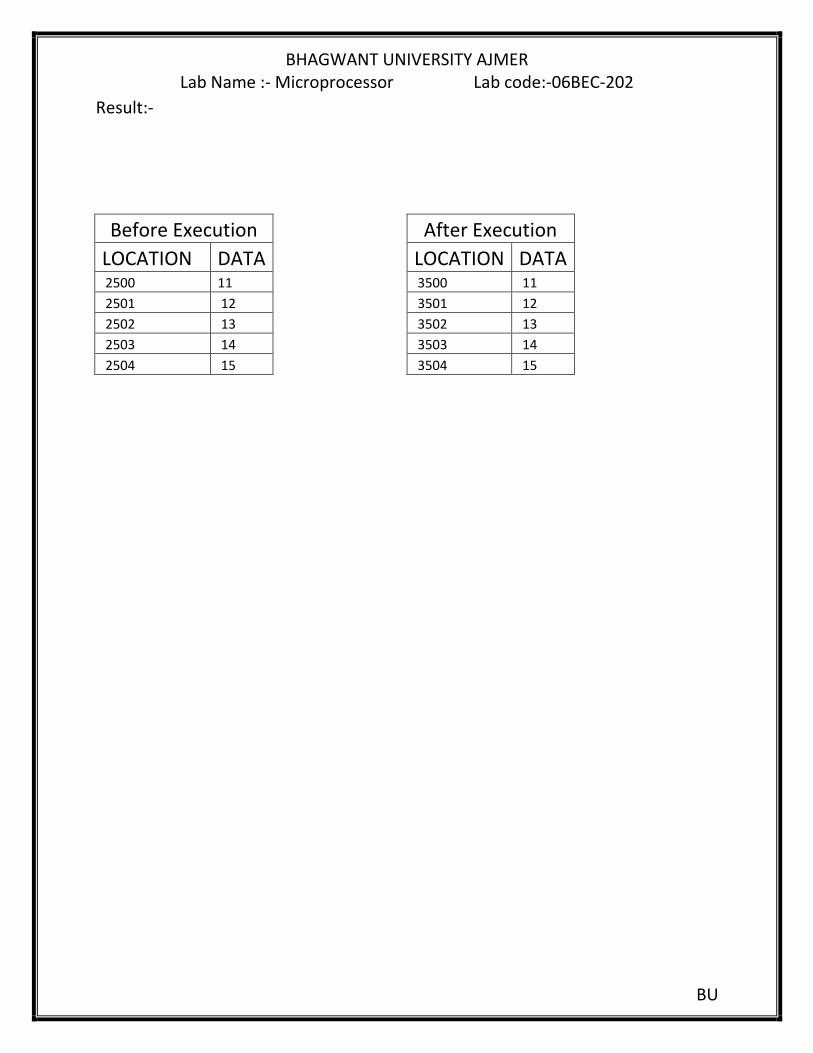
Result:-
Before Execution
After Execution
LOCATION DATA
LOCATION DATA 2500 11
3500 11
2501 12
3501 12
2502 13
3502 13
2503 14
3503 14
2504 15
3504 15

BHAGWANT UNIVERSITY AJMER Lab Name :- Microprocessor Lab code:-06BEC-202
BU
Experiment No:-4
Object:- Write a program to searching a no. in array & find the occurance of
that data.
Apparatus:- Vinytics VMC8509 Microprocessor Kit
Program:
Memory Address Mnemonics Label Hex
Code
2000 MVI D,00 16
2001
00
2002 LXI H 2500 21
2003 00
2004
25
2005 MOV C,M 4E
2006 INX H 23
2007 MOV A,M 7E
2008 INX H L1 23
2009 CMP M BE
200A JNZ 200E C2
200B 0E
200C
20
200D INR D 14
200E DCR C L2 0D
200F JNZ 2008
C2
2010
08
2011
20
2012 HLT
76

BHAGWANT UNIVERSITY AJMER Lab Name :- Microprocessor Lab code:-06BEC-202
BU
Result:-
Before Execution LOCATION DATA 2500 05 2501 02 2502 01 2503 02 2504 08 2505 02 2506 02
OUTPUT :- D=03

BHAGWANT UNIVERSITY AJMER Lab Name :- Microprocessor Lab code:-06BEC-202
BU
Experiment No:-5
Object:-write a Program to sort an arrary in ascending Order.
Apparatus:- Vinytics VMC 8509 Microprocessor Kit
Program:-
Memory Adderess Mnemonics Label
Hex Code
2000 LXI H,2500
21
2001 -
00
2002 -
25
2003 Mov C,M
4E
2004 MOV D,C
51
2005 INX H @ 23
2006 MOV A,M
7E
2007 INX H # 23
2008 MOV B,M
46
2009 CMP B
B8
200A JNC ($)
D2
200B
13
200C
20
200D DCX H
2B
200E MOV M,A
77
200F MOV A,B
78
2010 JMP*
C3
2011
15
2012
20

BHAGWANT UNIVERSITY AJMER Lab Name :- Microprocessor Lab code:-06BEC-202
BU
Result:-
2013 DCX H ($) 2B
Memory Adderess Mnemonics Label Hex Code
2014 MOV M,B
70
2015 INX H * 23
2016 DCR D
15
2017 JNZ#
C2
2018
07
2019
20
201A MoV M,A
77
201B DCR C
0D
201C JNZ@
C2
201D
05
201E
20
201F HLT
76
Before Execution
After Execution
Location Data
Location Data
2500 05
2500 02
2501 09
2501 03
2502 03
2502 04
2503 04
2503 05
2504 07
2504 07
2505 02
2505 09

BHAGWANT UNIVERSITY AJMER Lab Name :- Microprocessor Lab code:-06BEC-202
BU
Experiment No:-6
Object:- An Assembly Language Program to arrange an array of data in
descending order using 8085.
Apparatus: - 8085 Microprocessor Kit
Program:-
Algorithm
1) Initialize HL pair as memory pointer. 2) Get the count at 4200 in to C register. 3) Copy it in D register. 4) Get the first vale in Accumulator. 5) Compare it with the value at next location. 6) If they are out of order, exchange the contents of accumulator
and memory. 7) Decrement D register’s content by 1. 8) Repeat steps 5 and 7 till the value in D register become zero. 9) Decrement C register’s content by 1. 10) Repeat steps 3 to 9 till the value in C register becomes zero. 11) Terminate the program.
Program
MEMORY LABEL MNEMONIC HEX
CODE
COMMENT
4400 LXI H,4200 21
Load the array size to the HL pair 4401 00
4402 42
4403 MOV C,M 4E Copy the array size to C register
4404 DCR C 0D Decrement C by 1
4405 REPEAT MOV D,C 51 Copy content of C to D register
4406 LXI H,4201 21
Load the first data to the HL pair 4407 01
4408 42

BHAGWANT UNIVERSITY AJMER Lab Name :- Microprocessor Lab code:-06BEC-202
BU
4409 LOOP MOV A,M 7E Copy the data to the accumulator
440A INX H 23 Increment memory by 1
440B CMP M BE Compare accumulator and
memory content
440C JNC SKIP DA Jump on no carry to the label
SKIP 440D 14
440E 44
440F MOV B,M 46 Copy memory content to B
register
4410 MOV M,A 77 Copy accumulator content to
memory
4411 DCX H 2B Decrement memory by 1
4412 MOV M,B 70 Copy B register’s content to
memory
4413 INX H 23 Increment memory by 1
4414 SKIP DCR D 15 Decrement D by 1
4415 JNZ LOOP C2 Jump on non-zero to the label
LOOP 4416 09
4417 44
4418 DCR C 0D Decrement C by 1
4419 JNZ REPEAT C2 Jump on non-zero to the label
REPEAT 441A 05
441B 44
441C HLT 76 Program ends
Observation Input at 4200 : 05H ---------- Array Size 4201 : 01H 4202 : 02H 4203 : 03H 4204 : 04H 4205 : 05H Output at 4200 : 05H ---------- Array Size 4201 : 05H 4202 : 04H 4203 : 03H 4204 : 02H 4205 : 01H

BHAGWANT UNIVERSITY AJMER Lab Name :- Microprocessor Lab code:-06BEC-202
BU
EXPERIMENT NO.:-7
Object:- Write a program to perform BCD to Hexadecimal conversion.
Apparatus:- VINYTICS VMC 8509 Microprocessor Kit
Program:-
Memory Adderess Mnemonics Label Hex Code
F000 LXI H,F500 21
F001
00
F002
F5
F003 MOV A,M 7E
F004 ANI ,OF E6
F005 0F
F006 MOV B,A 47
F007 MOV A,M 7F
F008 ANI F0 E6
F009
F0
F00A RRC 0F
F00B RRC 0F
F00C RRC 0F
F00D RRC 0F
F00E MOV D,A 57
F00F MVI C,09
0E
F010
09
F011 ADD D # 82
F012 DCR C
0D
F013 JNZ #
C2

BHAGWANT UNIVERSITY AJMER Lab Name :- Microprocessor Lab code:-06BEC-202
BU
F014
11
F015
F0
F016 ADD B
80
F017 INX H
23
F018 MOV M,A
77
F019 HLT 76
RESULT:-
INPUT:- OUTPUT:-
F500:-25 F501:-19H

BHAGWANT UNIVERSITY AJMER Lab Name :- Microprocessor Lab code:-06BEC-202
BU
Experiment No:-8
Object:- Wirte a program to generate the Fibonicci No.
Apparatus:- Vinytics VMC8509 Microprocessor Kit
Program:
Memory Address Mnemonics Label Hex
Code
2000 LXI H,2500 21
2001 0
2002 25
2003 MOV C,M 4E
2004 INX H 23
2005 MOV A,M 0E
2006 INX H 23
2007 ADD M L1 BE
2008 INX H L2 DA
;2009 MOV M,A 10
200A DCX H 20
200B MOv A, M 96
200C DCR C 0C
200D JNZ C2
200E 06
200F 20
2010 HLT 76

BHAGWANT UNIVERSITY AJMER Lab Name :- Microprocessor Lab code:-06BEC-202
BU
EXPERIMENT No.:9
OBJECT:- Write a program to generate 15 Fibbonacci Number and sum
of 15 Fibbonacci
APPARATUS :- Vinytics VMC 8509 Microprocessor Kit
PROGRAM:-
Memory Adderess Mnemonics Label Hex Code
2000 LXI H,2500 21
2001 00
2002 25
2003 MOV C,M 4E
2004 INX H 23
2005 MOV A,M 7E
2006 INX H 23
2007 MVI B,01 06
2008 01
2009 ADD M @ 86
200A MOV D,A 57
200B ADD B 80
200C MOV B,A 47
200D INX H 23
200E MOV M,D 72
200F DCX H
2B
2010 MOV A,M
7E
2011 INX H
23
2012 DCR C
0D

BHAGWANT UNIVERSITY AJMER Lab Name :- Microprocessor Lab code:-06BEC-202
BU
2013 JNZ @
C2
2014
09
2015
20
2016 MOV A,B
78
2017 STA 2600
32
2018
00
2019
26
201A HLT
76
RESULT:-
INPUT:- OUTPUT:-
2500:- COUNT 2501 -00
2501 – 00 2502 - 01
2501 – 01 2503 -01
2504 – 02
2505 – 03
2506 – 05
2507 – 08
2508 – 0D

BHAGWANT UNIVERSITY AJMER Lab Name :- Microprocessor Lab code:-06BEC-202
BU
EXPERIMENT No.10
OBJECT:- Write a program for rolling disply of message “ INDIA”
APPARATUS :- Vinytics VMC 8509 Microprocessor Kit
PROGRAM:-
Memory Adderess Mnemonics Label
Hex Code
F000 LXI H, F500 # 21
F001 00
F002 F5
F003 PUSH H @ E5
F004 XRA A AF
F005 MOV B,A 47
F006 CALL (O/P) CD
F007 B7
F008 02
F009 MVI A,01 3E
F00A 01
F00B MVI B.00 06
F00C 00
F00D CALL (O/P) CD
F00E B7
F00F 02
F010 LXI D, FFFF H 11
F011 FF
F012 FF
F013 CALL (Delay) CD

BHAGWANT UNIVERSITY AJMER Lab Name :- Microprocessor Lab code:-06BEC-202
BU
F014 70
F015 F5
F016 MOV A,M 7E
F017 CPI FF FE
F018 FF
F019 POP H E1
F01A INX H 23
F01B JNZ @
C2
F01C
03
F01D
F0
F01E JMP #
C3
F01F
00
F020
F0
Delay Subroutine:-
Memory Adderess Mnemonics Label Hex Code
F570 DCX D @ 1B
F571 MOV A,D 7A
F572 ORA E B3
F573 JNZ @ C2
F574 70
F575 F5
F576 RET C9

BHAGWANT UNIVERSITY AJMER Lab Name :- Microprocessor Lab code:-06BEC-202
BU
EXPERIMENT No.11
OBJECT:- Programme to multiply two 8-bit numbers
Address Mnemonics Operand Opcode Remarks
2000 LXI H, 3000H 21 Load H-L pair with address 3000H.
2001 00 Lower-order of 3000H.
2002 30 Higher-order of 3000H.
2003 MOV B, M 46 Move the 1st operand from memory to reg. B.
2004 INX H 23 Increment H-L pair.
2005 MOV C, M 4E Move the 2nd operand from memory to reg. C.
2006 MVI A, 00H 3E Initialize accumulator with 00H.
2007 00 Immediate value 00H.
2008 ADD B 80 Add B with A.
2009 DCR C 0D Decrement reg. C (counter).
200A JNZ 2008H C2 Jump back to address 2008H if C ≠ 0.
200B 08 Lower-order of 2008H.
200C 20 Higher-order of 2008H.
200D INX H 23 Increment H-L pair.
200E MOV M, A 77 Move the result from accumulator to memory.
200F HLT 76 Halt.

BHAGWANT UNIVERSITY AJMER Lab Name :- Microprocessor Lab code:-06BEC-202
BU
Output:
Before Execution: 3000H: 02H
3001H: 05H After Execution: 3002H: 0AH