experimental study on carrier transport mechanism in
TRANSCRIPT

Experimental Study on Carrier Transport Mechanism in Ultrathin-body SOI MOSFETs
Ken Uchida*, Hiroshi Watanabe, Junji Koga, Atsuhiro Kinoshita, and Shin-ichi Takagi Advanced LSI Technology Laboratory, Toshiba Corp., 8, Shinsugita-cho, Isogo-ku, Yokohama 235-8522, Japan
*E-mail: [email protected]
Abstract— The electrical characteristics of ultrathin-body SOI CMOSFETs are intensively investigated. It is demonstrated that electron mobility increases as SOI thickness decreases, when SOI thickness, TSOI, is in the range from 3.5 nm to 4.5 nm. On the other hand, hole mobility decreases monotonically as TSOI decreases. In addition, it is demonstrated that, when SOI thickness is thinner than 4 nm, slight (even atomic-level) SOI thickness fluctuations have a significant impact on threshold voltage, gate-channel capacitance, and carrier mobility of ultrathin-body CMOSFETs.
Keywords- ultrathin-body, SOI, MOSFET, mobility, quantum-mechanical confinement
I. INTRODUCTION Ultrathin body (UTB) SOI MOSFETs are promising
candidates for a sub-30-nm MOSFET structure. In order to utilize the UTB MOSFETs in the deep-sub-20-nm regime, the realization of sub-5-nm SOI films is essential. Although much theoretical work has been done on the electrical characteristics of UTB MOSFETs [1-4], there are only a few experimental works [5-13]. Therefore, the electrical characteristics of UTB MOSFETs have not been fully understood yet.
In this report, the electrical characteristics of UTB CMOSFETs with SOI thickness, TSOI, ranging from 2.3 nm to 13 nm are intensively investigated. As a result, it is shown that electron mobility of UTB MOSFETs with TSOI of greater than 6 nm shows no TSOI dependence at low temperatures [14], indicating that the room-temperature mobility degradation in UTB MOSFETs with TSOI of less than 20 nm is mainly due to the phonon scattering. It is demonstrated for the first time that electron mobility increases as TSOI decreases, when TSOI is in the range from 3.5 nm to 4.5 nm [15]. It is also demonstrated that, when TSOI is thinner than 4 nm, slight (even atomic-level) SOI thickness fluctuations have a significant impact on threshold voltage, gate-channel capacitance, and carrier mobility of UTB CMOSFETs [15]. In addition, the relevance of a new type of scattering mechanism, that is, SOI-thickness-fluctuation- induced scattering is pointed out and experimentally verified [15].
II. DEVICE STRUCTURE Ultrathin-body (UTB) CMOSFETs with thick source and
drain regions were fabricated using UNIBOND wafers with 10Ωcm p-type 200-nm Si film over 400-nm buried oxide (Fig. 1). Fig. 2 shows a TEM image of a fabricated SOI channel, indicating the successful fabrication of ultrathin, 2.4-nm-thick
SOI channel. The SOI channels were left undoped for both n- and p-MOSFETs.
Since residual stress in the channel of MOSFETs strongly affects carrier mobility, residual stress in the ultrathin SOI channel should be evaluated. Raman spectra of ultrathin (5-nm and 7-nm) SOI layers were taken, utilizing slanting-polish-from-backside and laser-illumination-through-buried-oxide techniques. The schematic of the prepared sample is shown in the inset of Fig. 3. As shown in Fig, 3, the Raman spectra of ultrathin SOI films are almost the same as the Raman spectrum of bulk Si, indicating that there is no significant residual stress in the ultrathin SOI films.
n+n+ Gate
BOX
Substrate
70nm
400nm
500µm
0.5µm
n+ p+n+ Gate
BOX
p+FOXp- p-
500µm
0.5µm
nMOSFET pMOSFET
p-type 10Ωcm silicon-on-insulatorL/W = 500µm/200µm
TOX = 10nm, TSOI = 2.4nm ~ 13nm, TBOX=400nm Fig.1. Schematic of fabricated SOI CMOSFETs. The channel of both n- and p-MOSFETs is p-type 10Ωcm SOI, and its thickness is varied from 2.3 nm to 13 nm.
Gate Oxide
Buried Oxide
2.4nm
Fig.2. TEM image of fabricated SOI channel. Successful fabrication of ultrathin (2.4nm) SOI channel is confirmed.
SOIBuried OxideSubstrate
Gate OxideAluminum
He-Ne Laser(632.8nm)
Inte
nsity
[arb
. uni
ts.]
Ram an shift [cm -1]
TSOI=5nmTSOI=7nmBulk Si
480 500 520 540 5600
0.5
1
Fig. 3: Raman spectra of ultrathin SOIfilms. Raman spectrum of bulk Si isalso indicated as a reference. Thespectrum of the ultrathin SOI films issimilar to that of bulk Si, showing thatthere is no significant residual stress inultrathin SOI films.
0-7803-7826-1/03/$17.00 © 2003 IEEE- 8 -

III. TSOI DETERMINATION In order to investigate the TSOI dependence of UTB
CMOSFET characteristics, it is essential to precisely determine the thickness of SOI channel. Therefore, the relative comparison of SOI thickness is firstly performed using the substrate-bias-induced Vth shifts. Since the effect of substrate bias on the Vth shift is less in thinner body CMOSFETs, smaller Vth shift corresponds to thinner TSOI. Fig. 4 depicts the measured relationship between Vth’s and Vth shifts in UTB CMOSFETs. The Vth increase in thinner TSOI in both n- and p-MOSFETs suggests that the subband energy level increase is due to quantum-mechanical confinement effects in ultrathin SOI channel. The universal relationship between Vth’s and Vth shifts confirms that the variation of UTB CMOSFET characteristics is dominated by TSOI variation and that the variations of other device parameters, such as gate-oxide thickness, buried-oxide thickness, and substrate impurity concentration, are sufficiently suppressed and have negligible effects on UTB CMOSFET characteristics.
Next, in order to determine the actual SOI thickness, several TEM images are obtained, and the relationship between the TSOI’s and Vth shifts is empirically determined (Fig. 5). As a result, TSOI’s are now precisely estimated from the substrate-bias-induced Vth shift.
IV. MOBILITY CHARACTERISTICS First, the electrical characteristics of UTB nMOSFETs with
TSOI of greater than 8 nm are investigated. Fig. 6 shows effective electron mobility µeff versus effective field, Eeff, characteristics of UTB MOSFETs at room temperature. The mobility of a 68-nm SOI MOSFET almost coincides with the bulk universal mobility. This SOI MOS-FET is therefore referred to as a bulk-like SOI MOSFET in the following part of this article. The decrease of µeff with a decrease in TSOI is observed, which quantitatively agrees with the previously reported results [3,4].
In order to investigate the physical origin of µeff degradation, the µeff-Eeff characteristics were measured over wide temperature ranges in relatively thicker UTB SOI MOSFETs, whose SOI channel thickness in the range from 7 nm to 13 nm. As shown in Fig. 7, the difference of the mobility between the UTB MOSFETs and the bulk-like SOI-MOSFET becomes large in low Eeff regions as temperature decreases. However, at temperatures lower than 100K, the electron mobility of 8.7-nm and 12.4-nm UTB MOSFETs, whose mobility is lower than bulk-MOSFET mobility at room temperature, coincides with that of thick, bulk-like SOI-MOSFET, as shown in Fig. 8. This result indicates that, in UTB MOSFETs with TSOI of greater than 8 nm, 1) SOI
Thre
shol
d Vo
ltage
@
Ns=
5x10
11/c
m2
[V]
nMOS
pMOS
Vth Shift [V]
0.45
0.40
0.35
0.30
0.25
0.1240.1220.1200.1180.116
-1.55
-1.50
-1.45
-1.40
-1.35
-1.30
-1.25
0.1380.1360.1340.1320.130
TSOIThin Thick Fig.4. Threshold voltage shift versus threshold voltage of UTB CMOSFETs.
nMOS
Vth Shift [V]
T SO
I by
TEM
[nm
]
3.9e-11 exp(205.7x)+14.8x [nm]
0.116 0.12 0.1242
3
4
5
6
Fig.5. Threshold voltage shift versus SOI thickness measured by TEM.
Bulk universalTSOI = 7.0 nmTSOI = 8.7 nmTSOI = 12.4 nmTSOI = 68 nm
Electron Mobility [c
m2/Vsec]
Effective Field [MV/cm]
T=300K
0.1 1
1000
200
400
600
800
Fig. 6. Effective electron mobility versus transverseeffective field of ultrathin body (UTB) SOI MOSFETsfor various SOI thickness. The electron mobility of UTBMOSFETs decreases with a decrease in the SOI thickness.
Effective Field [MV/cm]Electron Mobility [c
m2/Vsec]
UniversalTSOI = 8.7 nmTSOI = 68 nm
100K
150K200K250K
300K
T = 100K - 300K
10-1 100102
103
Fig. 7. Effective electron mobility of ultrathin(TSOI=8.7nm) and thick (TSOI=68nm) SOI MOSFETs asa function of transverse effective field for varioustemperatures (100K ~ 300K). The mobility of the 8.7-nmUTB MOSFETs is less than that of the 68-nm, bulk-likeSOI MOSFET.
0-7803-7826-1/03/$17.00 © 2003 IEEE- 9 -
thickness of UTB MOSFETs is so uniform that there is no scattering center resulting from thickness fluctuations and that 2) the effect of Coulomb scattering and roughness scattering on the electron mobility in UTB MOSFETs with TSOI of greater than 8 nm is basically the same as that in bulk MOSFETs, at least at low temperatures. These results indicate that room-temperature mobility degradation in UTB MOSFETs is mainly caused by phonon scattering.
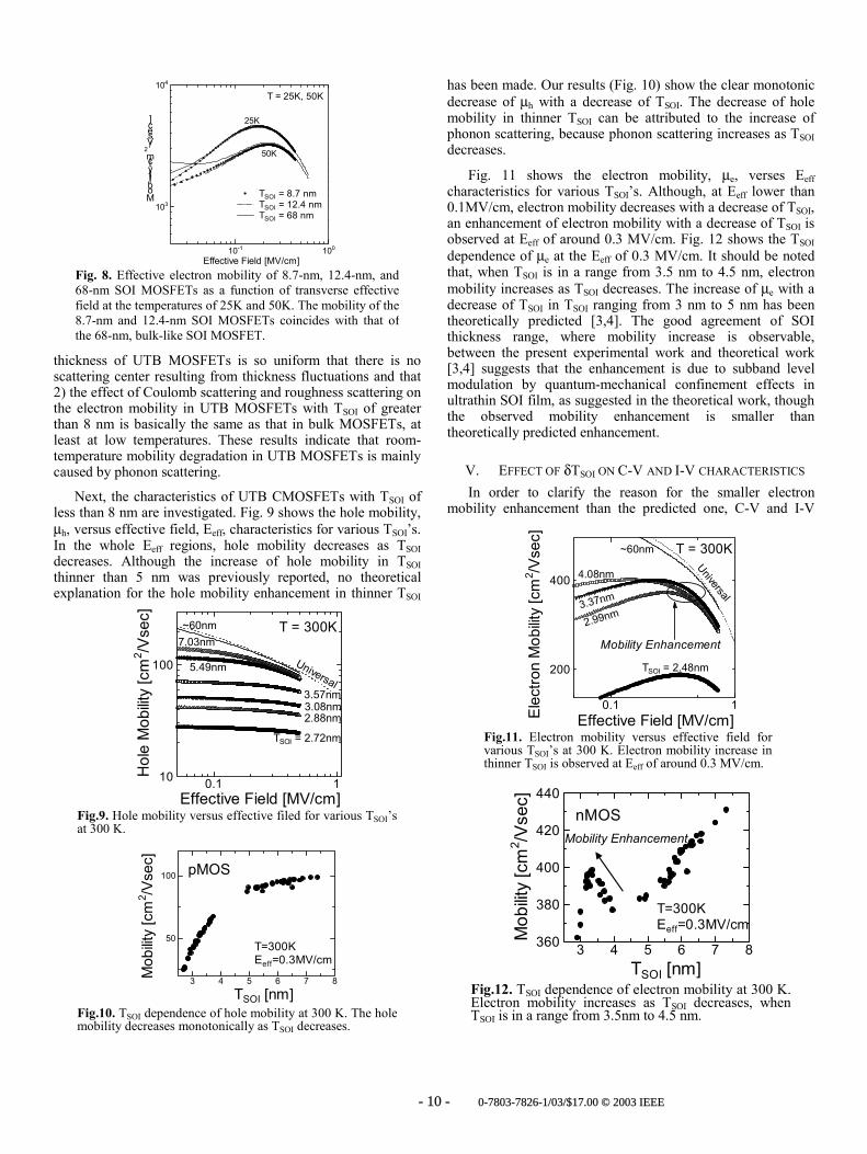
Next, the characteristics of UTB CMOSFETs with TSOI of less than 8 nm are investigated. Fig. 9 shows the hole mobility, µh, versus effective field, Eeff, characteristics for various TSOI’s. In the whole Eeff regions, hole mobility decreases as TSOI decreases. Although the increase of hole mobility in TSOI thinner than 5 nm was previously reported, no theoretical explanation for the hole mobility enhancement in thinner TSOI
has been made. Our results (Fig. 10) show the clear monotonic decrease of µh with a decrease of TSOI. The decrease of hole mobility in thinner TSOI can be attributed to the increase of phonon scattering, because phonon scattering increases as TSOI decreases.
Fig. 11 shows the electron mobility, µe, verses Eeff characteristics for various TSOI’s. Although, at Eeff lower than 0.1MV/cm, electron mobility decreases with a decrease of TSOI, an enhancement of electron mobility with a decrease of TSOI is observed at Eeff of around 0.3 MV/cm. Fig. 12 shows the TSOI dependence of µe at the Eeff of 0.3 MV/cm. It should be noted that, when TSOI is in a range from 3.5 nm to 4.5 nm, electron mobility increases as TSOI decreases. The increase of µe with a decrease of TSOI in TSOI ranging from 3 nm to 5 nm has been theoretically predicted [3,4]. The good agreement of SOI thickness range, where mobility increase is observable, between the present experimental work and theoretical work [3,4] suggests that the enhancement is due to subband level modulation by quantum-mechanical confinement effects in ultrathin SOI film, as suggested in the theoretical work, though the observed mobility enhancement is smaller than theoretically predicted enhancement.
V. EFFECT OF δTSOI ON C-V AND I-V CHARACTERISTICS
In order to clarify the reason for the smaller electron mobility enhancement than the predicted one, C-V and I-V
Effective Field [MV/cm]
Hol
e M
obilit
y [c
m2 /V
sec]
TSOI = 2.72nm
2.88nm3.08nm3.57nm
5.49nm
~60nm
Universal
T = 300K7.03nm
0.1 110
100
Fig.9. Hole mobility versus effective filed for various TSOI’sat 300 K.
Mob
ility
[cm
2 /Vse
c] pMOS
TSOI [nm]
T=300KEeff=0.3MV/cm
3 4 5 6 7 8
50
100
Fig.10. TSOI dependence of hole mobility at 300 K. The holemobility decreases monotonically as TSOI decreases.
Elec
tron
Mob
ility
[cm
2 /Vse
c]
Effective Field [MV/cm]
TSOI = 2.48nm
2.99nm3.37nm
4.08nm
T = 300K~60nm
Universal
Mobility Enhancement
0.1 1
200
400
Fig.11. Electron mobility versus effective field for various TSOI’s at 300 K. Electron mobility increase in thinner TSOI is observed at Eeff of around 0.3 MV/cm.
Mob
ility
[cm
2 /Vse
c]
TSOI [nm]
T=300KEeff=0.3MV/cm
nMOS
3 4 5 6 7 8360
380
400
420
440
Mobility Enhancement
Fig.12. TSOI dependence of electron mobility at 300 K.Electron mobility increases as TSOI decreases, whenTSOI is in a range from 3.5nm to 4.5 nm.
Effective Field [MV/cm]
Mobility [cm
2 /Vsec]
TSOI = 8.7 nmTSOI = 12.4 nmTSOI = 68 nm
25K
T = 25K, 50K
50K
10-1 100
103
104
Fig. 8. Effective electron mobility of 8.7-nm, 12.4-nm, and68-nm SOI MOSFETs as a function of transverse effectivefield at the temperatures of 25K and 50K. The mobility of the8.7-nm and 12.4-nm SOI MOSFETs coincides with that ofthe 68-nm, bulk-like SOI MOSFET.
0-7803-7826-1/03/$17.00 © 2003 IEEE- 10 -

characteristics of UTB CMOSFETs are thoroughly compared with self-consistent calculation results of Schrödinger and Poisson equations. In order to examine the influence of TSOI on Cgc with higher sensitivity, the derivative of Cgc with respect to Vg, that is, dCgc/dVg, is utilized. Fig. 13 shows TSOI dependence of dCgc/dVg. As shown in the figure, the increase of theoretical dCgc/dVg with a decrease of TSOI is clearly observed, which is due to the quantum-mechanical confinement effects of carriers in ultrathin SOI. However, when TSOI is thinner than 4 nm, experimental dCgc/dVg decreases with a decrease of TSOI.
Fig. 14 shows the TSOI dependence of Vth’s of UTB nMOSFETs. Although the experimental Vth’s agree well with theoretical ones when TSOI is greater than 4 nm, additional Vth increase is observed in TSOI of less than 4 nm. Fig. 15 shows Vth’s of UTB pMOSFETs as a function of TSOI. Additional Vth
increase compared to the theoretical one is also observed.
The degradation of dCgc/dVg and the additional Vth increase in thinner TSOI can be understood in terms of SOI thickness fluctuation, δTSOI. Since Si/SiO2 interface has ±1 atomic layer interface roughness, it is reasonable to assume that SOI has δTSOI of approximately 4 atomic layers (Fig. 16a). Fig. 16b shows changes in conduction band energy, ∆EC, induced by 4-atomic-layer δTSOI, as a function of average TSOI. When TSOI is thinner than 4 nm, ∆EC exceeds the thermal energy at room temperature, meaning that potential barriers due to difference of quantum-mechanical confinement effects from one part to another are formed in the ultrathin SOI channel (Fig. 16c). Therefore, in the case of UTB CMOSFETS having SOI fluctuations, higher gate voltage is necessary to obtain the same surface carrier concentration than in the case of UTB MOSFETs having no SOI fluctuation. As a result, Vth increase and slow Cgc rise are observed in UTB MOSFETs with SOI thickness fluctuations.
VI. EFFECT OF δTSOI ON MOBILITY CHARACTERISTICS
Next, the effect of SOI-thickness fluctuations on carrier mobility is discussed. Since the potential barriers shown in Fig. 16b are expected to work as scattering potential for carriers, µe and µh are expected to decrease as TSOI decreases. In fact, in GaAs/AlAs quantum wells, scattering by GaAs-width-fluctuation-induced potential is reported [16]. It is also reported that the width-fluctuation-limited mobility shows d6 dependence, where d is the GaAs channel width [16,17].
In order to examine whether this type of scattering is associated or not, µe for various TSOI’s is measured at low temperatures, because at low temperature phonon scattering is suppressed and the effect of thickness-fluctuation-induced scattering is observable more clearly. Fig. 17 shows µe-Eeff characteristics at 25 K, showing monotonic decrease of µe with a decrease of TSOI. Fig. 18 shows the TSOI dependence of µe at 25 K. The TSOI
6 dependence is clearly observed, meaning that
TSOI [nm]
dCgc
/dV g
[nF/
V]
TheoryExperimentT=300K
Decrease of dCgc/dVgin thinner TSOI
2 4 6 81.3
1.35
1.4
1.45
1.5
Fig.13. SOI thickness dependence of dCgc/dVg at Cgc of 150pF. Experimental and theoretical (self-consistent calculation) results are shown. Deviation from theoretical curve (degradation of dCgc/dVg) is clearly observed in TSOI thinner than approximately 4 nm.
TSOI [nm]V th @
Ns=
5x10
11/c
m2 [V
]
TheoryExperiment
Additional increase of Vthin thinner TSOI
T=300K
nMOS
2 4 6 80.2
0.25
0.3
0.35
0.4
Fig.14. TSOI dependence of nMOS Vth. Additional Vth increase is observed in TSOI thinner than 4nm.
TSOI [nm]-Vth
@N
s=5x
1011
/cm
2 [V]
Additional increase of Vthin thinner TSOI
T=300K
pMOS
TheoryExperiment
2 4 6 81.2
1.3
1.4
1.5
Fig. 15. TSOI dependence of pMOS Vth. Additional Vth increase is observed as in the case of nMOSFETs.
(c)
EF
EC
Potential barrier due to larger quantum confinement effect
Electrons
GOXSOIBOX
(a)
Interface roughnessThickness fluctuation
(b)
Thermal Energy∆EC [e
V]
TSOI [nm]2 4 6 8 100
0.05
0.1
0.15
Fig.16. (a) Si/SiO2 interface roughness induces SOI thickness fluctuations. (b) Variation of conduction band energy level due to SOI thickness fluctuation. The interface roughness of ±1atomic-layer per Si/SiO2 interface is assumed. (c) Schematics of EC variation effects.
0-7803-7826-1/03/$17.00 © 2003 IEEE- 11 -

in extremely thin SOI film the µe is dominated by scattering due to δTSOI-induced potential. Fig. 19 shows the temperature dependence of µe in nMOSFETs with TSOI of 2.48 nm. The temperature dependence is qualitatively the same as that of well-width-fluctuation-limited mobility in quantum wells [16]. Thus, it is concluded that this is the first observation of the relevance of a new type of scattering mechanism, namely δTSOI-induced scattering, peculiar to UTB MOSFETs. Fig. 20 shows the µh-Eeff characteristics at 25 K. The rapid decrease of µh in thinner TSOI suggests that δTSOI-induced scattering is also influential to pMOSFETs. Fig. 21 shows the µe-Eeff characteristics, where δTSOI-fluctuation-induced scattering is subtracted using Mathiessen’s rule. The increase of µe with a decrease of TSOI is clearly observed in the whole Eeff region, when TSOI changes from 4.08 nm to 3.37 nm. Therefore, it is concluded that the realization of atomically flat SOI is vital (Fig. 22), in order to enjoy the full advantages of UTB CMOSFETs in deep-sub-20-nm regime.
VII. CONCLUSION The carrier transport mechanism in UTB CMOSFETs with
TSOI ranging from 2.3 nm to 13 nm is investigated. It is demonstrated, for the first time, that electron mobility increases as TSOI decreases, when TSOI is in the range from 3.5 nm to 4.5 nm, because of subband-energy modulation effects. It is also demonstrated that, when TSOI is extremely thin (<4nm), slight (even atomic-level) TSOI fluctuations have a significant impact on Vth and Cgc of UTB CMOSFETs. In addition, δTSOI-induced
Temperature [K]
Mob
ility
[cm
2 /Vse
c]
TSOI=2.48nm
Eeff=0.1MV/cm
10 100100
200
300
Fig.19. Temperature dependence of electron mobility of2.4-nm-thick SOI nMOSFET at Eeff of 0.1 MV/cm. Thetemperature dependence is qualitatively the same as thatof the well-width-fluctuation-limited mobility inGaAs/AlAs quantum-wells [5].
3.57nm3.08nm2.88nm
TSOI = 2.72nm
Effective Field [MV/cm]
Hol
e M
obilit
y [c
m2 /V
sec] T = 25K
~60nm
5.49nm
7.03nm
0.1 110
100
1000
Fig.20. Hole mobility versus effective field at 25 K.
M
obilit
y [c
m2 /V
sec]
Effective Field [MV/cm]
TSOI=2.48nm
T=300K
4.08nm
3.37nm
Effect of thicknes fluctuation issubtracted
10.2 0.4 0.6 0.8
200
400
600Mobility increase with a decrease of TSOI
Fig.21. Effective field dependence of electronmobility, where the effect of thickness fluctuation issubtracted.
8
6
4
2
δTSO
I [at
omic
laye
r]
765432TSOI [nm]
δδδδTSOI should be smaller than this line.
Fig. 22. Requirements for SOI thickness fluctuation, δTSOI, as a function of TSOI, calculated on the assumption that ∆EC should be smaller than the half of thermal energy at room temperature. 1-atomic layer corresponds to approximately 0.28nm
TSOI = 2.48nm2.99nm3.37nm
4.08nm
5.7nm
~60nm
T = 25K
Effective Field [MV/cm]Elec
tron
Mob
ility
[cm
2 /Vse
c]7.2nm
0.1 1100
1000
Fig.17. Electron mobility versus effective field at 25K.Electron mobility decreases in the whole Eeff regions whenTSOI is thinner than approximately 4nm.
TSOI [nm]
Mob
ility
[cm
2 /Vse
c]
∝TSOI6
T=25KEeff=0.1MV/cm
2 3 4100
1000
Fig.18. TSOI dependence of electron mobility at 25 K.TSOI
6 dependence indicates that the dominant scatteringmechanism is TSOI-fluctuation- induced scattering.
0-7803-7826-1/03/$17.00 © 2003 IEEE- 12 -

scattering, which is a new scattering mechanism to strongly limit the mobility of UTB MOSFETs with TSOI of less than 3nm, is observed, for the first time. It should be noted that this type of scattering also limits the mobility of other thin-channel MOSFETs, such as FinFETs [18]. It is concluded that the realization of atomically flat SOI is vital, in order to enjoy the full advantages of UTB CMOSFETs, such as electron mobility enhancement and larger Cgc rise, in deep-sub-20-nm regime.
ACKNOWLEDGEMENT This work was performed under the management of JEITA,
which is supported by NEDO.
REFERENCES [1] D. Esseni, A. Abramo, L. Selmi, and E. Sangiorgi, Tech. Dig. Int.
Electron Devices Meet. (2002), p.719. [2] F. Gámiz, J. B. Roldán, J. A. López-Villanueva, P. Catrujo-Cassinello,
and J. E. Carceller, J. Appl. Phys., 86, 6854, 1999. [3] M. Shoji and S. Horiguchi, J. Appl. Phys., 85, 2722, 1999. [4] S. Takagi, J. Koga, and A. Toriumi, Tech. Dig. Int. Electron Devices
Meet. (1997), p.219. [5] Y. Omura, S. Horiguchi, M. Tabe, and K. Kishi, IEEE Electron Device
Lett., 14, 569, 1993. [6] J. Wang, N. Kistler, J. Woo, and C. R. Viswanathan, IEEE Electron
Device Lett., 15, 117, 1994. [7] J.-H. Choi, Y.-J. Park, and H.-S. Min, IEEE Electron Device Lett., 16,
527, 1995. [8] A. Toriumi, J. Koga, H. Satake, and A. Ohata, Tech. Dig. of Int.
Electron Devices Meet. (1995), p.847. [9] D. Esseni, M. Mastrapasqua, G. K. Celler, F. H. Baumann, C. Fiegna, L.
Selmi, and E. Sangiorgi, Tech. Dig. Int. Electron Devices Meet. (2000), p.671.
[10] D. Esseni, Tech. Dig. Int. Electron Devices Meet. (2001), p.445. [11] J. Koga, S. Takagi, and A. Toriumi, IEEE Trans. Electron Devices, 49,
1042, 2002. [12] Z. Ren, P. Solomon, T. Kanarsky, B. Doris, O. Dokumaci, P. Oldiges, R.
Roy, E. Jones, M. Ieong, R. Miller, W. Haensch, H. Whong, Tech. Dig. Int. Electron Devices Meet. (2002), p.51.
[13] T. Ernst, D. Munteanu, S. Cristoloveanu, T. Ouisse, S. Horiguchi, Y. Ono, Y. Takahashi, and K. Murase, Microelectronic Eng., 48, 339, 1999.
[14] K. Uchida, J. Koga, R. Ohba, T. Numata, and S. Takagi, Tech. Dig. of Int. Electron Devices Meet. (2001), p.633.
[15] K. Uchida, H. Watanabe, A. Kinoshita, J. Koga, T. Numata, and S. Takagi, Tech. Dig. of Int. Electron Devices Meet. (2002), p.47.
[16] H. Sakaki, T. Noda, K. Hirakawa, M. Tanaka, and T. Matsusue, Appl. Phys. Lett., 51, 1934, 1987.
[17] A. Gold, Phys. Rev. B, 35, 723, 1987. [18] D. Hisamoto, W.-C. Lee, J. Kedzierski, H. Takeuchi, K. Asano, C. Kuo,
R. Anderson, T.-J. King, J. Bokor, and C. Hu, IEEE Trans. Electron Devices, 47, 2320, 2000.
0-7803-7826-1/03/$17.00 © 2003 IEEE- 13 -