external memory interface handbook...external memory interface handbook volume 3: reference material...
TRANSCRIPT

External Memory Interface HandbookVolume 3: Reference Material
Last updated for Altera Complete Design Suite: 14.1
Subscribe
Send Feedback
EMI_RM2014.12.15
101 Innovation DriveSan Jose, CA 95134www.altera.com

Contents
Functional Description—UniPHY......................................................................1-1I/O Pads.........................................................................................................................................................1-2Reset and Clock Generation....................................................................................................................... 1-3Dedicated Clock Networks......................................................................................................................... 1-3Address and Command Datapath............................................................................................................. 1-4Write Datapath.............................................................................................................................................1-5
Leveling Circuitry............................................................................................................................ 1-5Read Datapath.............................................................................................................................................. 1-7Sequencer...................................................................................................................................................... 1-8
Nios II-Based Sequencer................................................................................................................. 1-9RTL-based Sequencer....................................................................................................................1-13
Shadow Registers........................................................................................................................................1-15Shadow Registers Operation........................................................................................................ 1-17
UniPHY Interfaces.....................................................................................................................................1-17The DLL and PLL Sharing Interface........................................................................................... 1-18The OCT Sharing Interface.......................................................................................................... 1-19
UniPHY Signals..........................................................................................................................................1-21PHY-to-Controller Interfaces.................................................................................................................. 1-25Using a Custom Controller...................................................................................................................... 1-30AFI 4.0 Specification..................................................................................................................................1-31
Bus Width and AFI Ratio............................................................................................................. 1-32AFI Parameters...............................................................................................................................1-32AFI Signals...................................................................................................................................... 1-34
Register Maps............................................................................................................................................. 1-41UniPHY Register Map...................................................................................................................1-42Controller Register Map............................................................................................................... 1-45
Ping Pong PHY.......................................................................................................................................... 1-46Ping Pong PHY Feature Description.......................................................................................... 1-46Ping Pong PHY Architecture....................................................................................................... 1-47Ping Pong PHY Operation........................................................................................................... 1-49
Efficiency Monitor and Protocol Checker..............................................................................................1-50Efficiency Monitor.........................................................................................................................1-50Protocol Checker............................................................................................................................1-50Read Latency Counter................................................................................................................... 1-50Using the Efficiency Monitor and Protocol Checker................................................................1-50Avalon CSR Slave and JTAG Memory Map...............................................................................1-51
UniPHY Calibration Stages......................................................................................................................1-53Calibration Overview.................................................................................................................... 1-54Calibration Stages.......................................................................................................................... 1-54Memory Initialization................................................................................................................... 1-55Stage 1: Read Calibration Part One—DQS Enable Calibration and DQ/DQS Centering...1-55Stage 2: Write Calibration Part One............................................................................................1-59
TOC-2 External Memory Interface Handbook Volume 3: Reference Material
Altera Corporation

Stage 3: Write Calibration Part Two—DQ/DQS Centering.................................................... 1-61Stage 4: Read Calibration Part Two—Read Latency Minimization........................................1-61Calibration Signals.........................................................................................................................1-61Calibration Time............................................................................................................................1-61
Document Revision History.....................................................................................................................1-62
Functional Description—Arria 10 EMIF............................................................2-1Supported Memory Protocols.................................................................................................................... 2-2Key Differences Compared to UniPHY IP and Previous Device Families.......................................... 2-2Migrating from Previous Device Families................................................................................................2-2Arria 10 EMIF Architecture: Introduction...............................................................................................2-3
Arria 10 EMIF Architecture: I/O Subsystem............................................................................... 2-4Arria 10 EMIF Architecture: I/O Column....................................................................................2-4Arria 10 EMIF Architecture: I/O AUX......................................................................................... 2-5Arria 10 EMIF Architecture: I/O Bank......................................................................................... 2-5Arria 10 EMIF Architecture: I/O Lane..........................................................................................2-8Arria 10 EMIF Architecture: Input DQS Clock Tree............................................................... 2-11Arria 10 EMIF Architecture: PHY Clock Tree.......................................................................... 2-12Arria 10 EMIF Architecture: PLL Reference Clock Networks................................................ 2-12Arria 10 EMIF Architecture: Clock Phase Alignment..............................................................2-13
Hardware Resource Sharing Among Multiple EMIFs..........................................................................2-14I/O Aux Sharing............................................................................................................................. 2-15I/O Bank Sharing........................................................................................................................... 2-15PLL Reference Clock Sharing.......................................................................................................2-16Core Clock Network Sharing....................................................................................................... 2-17RZQ Pin Sharing............................................................................................................................ 2-17
Arria 10 EMIF IP Component................................................................................................................. 2-17Instantiating Your Arria 10 EMIF IP in a Qsys Project............................................................2-18File Sets............................................................................................................................................2-21Customized readme.txt File..........................................................................................................2-22Clock Domains...............................................................................................................................2-22ECC in Arria 10 EMIF IP..............................................................................................................2-23
Examples of External Memory Interface Implementations for DDR4.............................................. 2-24Arria 10 EMIF Sequencer......................................................................................................................... 2-29Arria 10 EMIF Calibration....................................................................................................................... 2-30
Calibration Stages ......................................................................................................................... 2-30Calibration Stages Descriptions................................................................................................... 2-31Calibration Algorithms................................................................................................................. 2-32Calibration Flowchart................................................................................................................... 2-34
Hard Memory Controller Rate Conversion Feature.............................................................................2-34Compiling Arria 10 EMIF IP with the Quartus II Software................................................................ 2-35
Instantiating the Arria 10 EMIF IP............................................................................................. 2-35Setting I/O Assignments in Arria 10 EMIF IP...........................................................................2-35
Debugging Arria 10 EMIF IP................................................................................................................... 2-35External Memory Interface Debug Toolkit................................................................................2-36On-Chip Debug for Arria 10........................................................................................................2-36Configuring Your EMIF IP for Use with the Debug Toolkit...................................................2-36Arria 10 EMIF Debugging Examples.......................................................................................... 2-37
External Memory Interface Handbook Volume 3: Reference Material TOC-3
Altera Corporation

Arria 10 EMIF for Hard Processor Subsystem...................................................................................... 2-39Restrictions on I/O Bank Usage for Arria 10 EMIF IP with HPS........................................... 2-40
Arria 10 EMIF Ping Pong PHY................................................................................................................2-42Ping Pong PHY Feature Description.......................................................................................... 2-42Ping Pong PHY Architecture....................................................................................................... 2-44Ping Pong PHY Limitations......................................................................................................... 2-45Ping Pong PHY Calibration......................................................................................................... 2-47Using the Ping Pong PHY............................................................................................................ 2-47Ping Pong PHY Simulation Example Design............................................................................ 2-47
AFI 4.0 Specification..................................................................................................................................2-48Bus Width and AFI Ratio............................................................................................................. 2-48AFI Parameters...............................................................................................................................2-48AFI Signals...................................................................................................................................... 2-50
Memory Mapped Register (MMR) Tables............................................................................................. 2-57ctrlcfg0: Controller Configuration.............................................................................................. 2-59ctrlcfg1: Controller Configuration.............................................................................................. 2-61ctrlcfg2: Controller Configuration.............................................................................................. 2-63ctrlcfg3: Controller Configuration.............................................................................................. 2-64ctrlcfg4: Controller Configuration.............................................................................................. 2-65ctrlcfg5: Controller Configuration.............................................................................................. 2-66ctrlcfg6: Controller Configuration.............................................................................................. 2-67ctrlcfg7: Controller Configuration.............................................................................................. 2-67ctrlcfg8: Controller Configuration.............................................................................................. 2-68ctrlcfg9: Controller Configuration.............................................................................................. 2-68dramtiming0: Timing Parameters............................................................................................... 2-68dramodt0: On-Die Termination Parameters............................................................................. 2-69dramodt1: On-Die Termination Parameters............................................................................. 2-69sbcfg0: Sideband Configuration...................................................................................................2-70sbcfg1: Sideband Configuration...................................................................................................2-70sbcfg2: Sideband Configuration...................................................................................................2-70sbcfg3: Sideband Configuration...................................................................................................2-71sbcfg4: Sideband Configuration...................................................................................................2-71sbcfg5: Sideband Configuration...................................................................................................2-71sbcfg6: Sideband Configuration...................................................................................................2-72sbcfg7: Sideband Configuration...................................................................................................2-72sbcfg8: Sideband Configuration...................................................................................................2-72sbcfg9: Sideband Configuration...................................................................................................2-73caltiming0: Command/Address/Latency Parameters...............................................................2-73caltiming1: Command/Address/Latency Parameters...............................................................2-73caltiming2: Command/Address/Latency Parameters...............................................................2-74caltiming3: Command/Address/Latency Parameters...............................................................2-74caltiming4: Command/Address/Latency Parameters...............................................................2-75caltiming5: Command/Address/Latency Parameters...............................................................2-75caltiming6: Command/Address/Latency Parameters...............................................................2-75caltiming7: Command/Address/Latency Parameters...............................................................2-75caltiming8: Command/Address/Latency Parameters...............................................................2-76caltiming9: Command/Address/Latency Parameters...............................................................2-76caltiming10: Command/Address/Latency Parameters.............................................................2-77dramaddrw: Row/Column/Bank Address Width Configuration........................................... 2-77
TOC-4 External Memory Interface Handbook Volume 3: Reference Material
Altera Corporation

sideband0: Sideband...................................................................................................................... 2-77sideband1: Sideband...................................................................................................................... 2-77sideband2: Sideband...................................................................................................................... 2-78sideband3: Sideband...................................................................................................................... 2-78sideband4: Sideband...................................................................................................................... 2-78sideband5: Sideband...................................................................................................................... 2-78sideband6: Sideband...................................................................................................................... 2-79sideband7: Sideband...................................................................................................................... 2-79sideband8: Sideband...................................................................................................................... 2-79sideband9: Sideband...................................................................................................................... 2-79sideband10: Sideband....................................................................................................................2-79sideband11: Sideband....................................................................................................................2-80sideband12: Sideband....................................................................................................................2-80sideband13: Sideband....................................................................................................................2-80sideband14: Sideband....................................................................................................................2-81sideband15: Sideband....................................................................................................................2-81dramsts: Calibration Status...........................................................................................................2-81
Document Revision History.....................................................................................................................2-82
Functional Description—MAX 10 EMIF............................................................3-1MAX 10 EMIF Overview............................................................................................................................ 3-1External Memory Protocol Support.......................................................................................................... 3-2MAX 10 Memory Controller......................................................................................................................3-2MAX 10 Memory PHY................................................................................................................................3-2
Supported Topologies..................................................................................................................... 3-3Read Datapath.................................................................................................................................. 3-3Write Datapath.................................................................................................................................3-4Address and Command Datapath................................................................................................. 3-6Sequencer.......................................................................................................................................... 3-7
Calibration.................................................................................................................................................... 3-9Read Calibration............................................................................................................................ 3-10Write Calibration........................................................................................................................... 3-10
Sequencer Debug Information.................................................................................................................3-10Register Maps............................................................................................................................................. 3-12Document Revision History.....................................................................................................................3-12
Functional Description—Hard Memory Interface.............................................4-1Multi-Port Front End (MPFE)...................................................................................................................4-2Multi-port Scheduling.................................................................................................................................4-3
Port Scheduling................................................................................................................................ 4-3DRAM Burst Scheduling.................................................................................................................4-3DRAM Power Saving Modes..........................................................................................................4-4
MPFE Signal Descriptions.......................................................................................................................... 4-4Hard Memory Controller........................................................................................................................... 4-7
Clocking............................................................................................................................................ 4-8Reset................................................................................................................................................... 4-8DRAM Interface...............................................................................................................................4-8
External Memory Interface Handbook Volume 3: Reference Material TOC-5
Altera Corporation

ECC.................................................................................................................................................... 4-8Bonding of Memory Controllers................................................................................................... 4-9
Hard PHY................................................................................................................................................... 4-10Interconnections............................................................................................................................ 4-10Clock Domains...............................................................................................................................4-11Hard Sequencer..............................................................................................................................4-11MPFE Setup Guidelines................................................................................................................ 4-11Soft Memory Interface to Hard Memory Interface Migration Guidelines............................4-12Bonding Interface Guidelines.......................................................................................................4-13
Document Revision History.....................................................................................................................4-13
Functional Description—HPS Memory Controller........................................... 5-1Features of the SDRAM Controller Subsystem....................................................................................... 5-1SDRAM Controller Subsystem Block Diagram.......................................................................................5-2SDRAM Controller Memory Options...................................................................................................... 5-3SDRAM Controller Subsystem Interfaces................................................................................................ 5-4
MPU Subsystem Interface.............................................................................................................. 5-4L3 Interconnect Interface................................................................................................................5-4CSR Interface.................................................................................................................................... 5-5FPGA-to-HPS SDRAM Interface.................................................................................................. 5-5
Memory Controller Architecture.............................................................................................................. 5-6Multi-Port Front End...................................................................................................................... 5-7Single-Port Controller..................................................................................................................... 5-8
Functional Description of the SDRAM Controller Subsystem........................................................... 5-10MPFE Operation Ordering...........................................................................................................5-10MPFE Multi-Port Arbitration......................................................................................................5-10MPFE SDRAM Burst Scheduling................................................................................................ 5-13Single-Port Controller Operation................................................................................................5-14
SDRAM Power Management...................................................................................................................5-24DDR PHY................................................................................................................................................... 5-25Clocks.......................................................................................................................................................... 5-25Resets........................................................................................................................................................... 5-26
Taking the SDRAM Controller Subsystem Out of Reset ........................................................ 5-26Port Mappings............................................................................................................................................5-26Initialization................................................................................................................................................5-27
FPGA-to-SDRAM Protocol Details............................................................................................ 5-27SDRAM Controller Subsystem Programming Model.......................................................................... 5-33
HPS Memory Interface Architecture.......................................................................................... 5-33HPS Memory Interface Configuration....................................................................................... 5-33HPS Memory Interface Simulation............................................................................................. 5-34Generating a Preloader Image for HPS with EMIF...................................................................5-34
Debugging HPS SDRAM in the Preloader.............................................................................................5-36Enabling UART or Semihosting Printout.................................................................................. 5-36Enabling Simple Memory Test.....................................................................................................5-37Enabling the Debug Report.......................................................................................................... 5-38Writing a Predefined Data Pattern to SDRAM in the Preloader............................................ 5-41
SDRAM Controller Address Map and Register Definitions................................................................5-42SDRAM Controller Address Map............................................................................................... 5-42
TOC-6 External Memory Interface Handbook Volume 3: Reference Material
Altera Corporation

Document Revision History.....................................................................................................................5-72
Functional Description—HPC II Controller......................................................6-1HPC II Memory Interface Architecture................................................................................................... 6-1HPC II Memory Controller Architecture.................................................................................................6-2
Backpressure Support......................................................................................................................6-4Command Generator...................................................................................................................... 6-5Timing Bank Pool............................................................................................................................ 6-5Arbiter................................................................................................................................................6-5Rank Timer....................................................................................................................................... 6-5Read Data Buffer and Write Data Buffer......................................................................................6-5ECC Block......................................................................................................................................... 6-5AFI and CSR Interfaces...................................................................................................................6-6
HPC II Controller Features........................................................................................................................ 6-6Data Reordering............................................................................................................................... 6-6Pre-emptive Bank Management.................................................................................................... 6-6Quasi-1T and Quasi-2T.................................................................................................................. 6-6User Autoprecharge Commands................................................................................................... 6-7Address and Command Decoding Logic......................................................................................6-7Low-Power Logic............................................................................................................................. 6-7ODT Generation Logic....................................................................................................................6-7Burst Merging.................................................................................................................................6-10ECC.................................................................................................................................................. 6-10
External Interfaces..................................................................................................................................... 6-13Clock and Reset Interface............................................................................................................. 6-13Avalon-ST Data Slave Interface................................................................................................... 6-13AXI Data Slave Interface...............................................................................................................6-13Controller-PHY Interface............................................................................................................. 6-21Memory Side-Band Signals...........................................................................................................6-21Controller External Interfaces......................................................................................................6-22
Top-Level Signals Description................................................................................................................. 6-23Clock and Reset Signals.................................................................................................................6-23Local Interface Signals...................................................................................................................6-25Controller Interface Signals..........................................................................................................6-31CSR Interface Signals.....................................................................................................................6-33Soft Controller Register Map........................................................................................................6-34Hard Controller Register Map..................................................................................................... 6-41
Sequence of Operations............................................................................................................................ 6-45Document Revision History.....................................................................................................................6-46
Functional Description—QDR II Controller..................................................... 7-1Block Description.........................................................................................................................................7-1
Avalon-MM Slave Read and Write Interfaces............................................................................. 7-1Command Issuing FSM.................................................................................................................. 7-2AFI......................................................................................................................................................7-2
Avalon-MM and Memory Data Width.....................................................................................................7-2Signal Descriptions...................................................................................................................................... 7-3
External Memory Interface Handbook Volume 3: Reference Material TOC-7
Altera Corporation

Document Revision History.......................................................................................................................7-4
Functional Description—QDR IV Controller....................................................8-1Block Description.........................................................................................................................................8-1
Avalon-MM Slave Read and Write Interfaces............................................................................. 8-1AFI......................................................................................................................................................8-2
Avalon-MM and Memory Data Width.....................................................................................................8-2Signal Descriptions...................................................................................................................................... 8-3Document Revision History.......................................................................................................................8-4
Functional Description—RLDRAM II Controller............................................. 9-1Block Description.........................................................................................................................................9-1
Avalon-MM Slave Interface............................................................................................................9-1Write Data FIFO Buffer.................................................................................................................. 9-2Command Issuing FSM.................................................................................................................. 9-2Refresh Timer................................................................................................................................... 9-2Timer Module...................................................................................................................................9-2AFI......................................................................................................................................................9-2
User-Controlled Features........................................................................................................................... 9-3Error Detection Parity.....................................................................................................................9-3User-Controlled Refresh................................................................................................................. 9-3
Avalon-MM and Memory Data Width.....................................................................................................9-3Signal Descriptions...................................................................................................................................... 9-3Document Revision History.......................................................................................................................9-4
Functional Description—RLDRAM 3 PHY-Only IP....................................... 10-1Block Description.......................................................................................................................................10-1Features....................................................................................................................................................... 10-1RLDRAM 3 AFI Protocol......................................................................................................................... 10-2RLDRAM 3 Controller with Arria 10 EMIF Interfaces........................................................................10-3Document Revision History.....................................................................................................................10-5
Functional Description—Example Designs......................................................11-1UniPHY-Based Example Designs............................................................................................................11-1
Synthesis Example Design............................................................................................................ 11-1Simulation Example Design......................................................................................................... 11-3Traffic Generator and BIST Engine.............................................................................................11-5Creating and Connecting the UniPHY Memory Interface and the Traffic Generator in
Qsys............................................................................................................................................ 11-9Arria 10 EMIF IP Example Designs...................................................................................................... 11-10
Synthesizable Example Design...................................................................................................11-10Simulation Example Design....................................................................................................... 11-11
Document Revision History...................................................................................................................11-11
Introduction to UniPHY IP.............................................................................. 12-1
TOC-8 External Memory Interface Handbook Volume 3: Reference Material
Altera Corporation

Release Information...................................................................................................................................12-1Device Support Levels............................................................................................................................... 12-2Device Family and Protocol Support...................................................................................................... 12-2UniPHY-Based External Memory Interface Features.......................................................................... 12-3System Requirements................................................................................................................................ 12-5MegaCore Verification..............................................................................................................................12-6Resource Utilization.................................................................................................................................. 12-6
DDR2, DDR3, and LPDDR2 Resource Utilization in Arria V Devices................................. 12-6DDR2 and DDR3 Resource Utilization in Arria II GZ Devices..............................................12-7DDR2 and DDR3 Resource Utilization in Stratix III Devices.................................................12-9DDR2 and DDR3 Resource Utilization in Stratix IV Devices...............................................12-11DDR2 and DDR3 Resource Utilization in Arria V GZ and Stratix V Devices................... 12-13QDR II and QDR II+ Resource Utilization in Arria V Devices............................................12-16QDR II and QDR II+ Resource Utilization in Arria II GX Devices..................................... 12-17QDR II and QDR II+ Resource Utilization in Arria II GZ, Arria V GZ, Stratix III,
Stratix IV, and Stratix V Devices..........................................................................................12-17RLDRAM II Resource Utilization in Arria V Devices............................................................12-18RLDRAM II Resource Utilization in Arria II GZ, Arria V GZ, Stratix III, Stratix IV, and
Stratix V Devices.................................................................................................................... 12-18Document Revision History...................................................................................................................12-19
Latency for UniPHY IP..................................................................................... 13-1DDR2 SDRAM LATENCY...................................................................................................................... 13-1DDR3 SDRAM LATENCY...................................................................................................................... 13-2LPDDR2 SDRAM LATENCY..................................................................................................................13-3QDR II and QDR II+ SRAM Latency..................................................................................................... 13-4RLDRAM II Latency..................................................................................................................................13-5RLDRAM 3 Latency.................................................................................................................................. 13-5Variable Controller Latency..................................................................................................................... 13-6Document Revision History.....................................................................................................................13-6
Timing Diagrams for UniPHY IP.....................................................................14-1DDR2 Timing Diagrams...........................................................................................................................14-1DDR3 Timing Diagrams...........................................................................................................................14-7QDR II and QDR II+ Timing Diagrams.............................................................................................. 14-15RLDRAM II Timing Diagrams.............................................................................................................. 14-19LPDDR2 Timing Diagrams....................................................................................................................14-24RLDRAM 3 Timing Diagrams...............................................................................................................14-30Document Revision History...................................................................................................................14-34
External Memory Interface Debug Toolkit...................................................... 15-1Architecture................................................................................................................................................ 15-1
Communication............................................................................................................................. 15-1Calibration and Report Generation.............................................................................................15-2
Setup and Use............................................................................................................................................. 15-2General Workflow......................................................................................................................... 15-3
External Memory Interface Handbook Volume 3: Reference Material TOC-9
Altera Corporation

Linking the Project to a Device.................................................................................................... 15-3Establishing Communication to Connections...........................................................................15-4Selecting an Active Interface........................................................................................................ 15-4Reports.............................................................................................................................................15-4
Operational Considerations..................................................................................................................... 15-6Troubleshooting.........................................................................................................................................15-7EMIF On-Chip Debug Toolkit................................................................................................................ 15-7
Access Protocol.............................................................................................................................. 15-8Command Codes Reference......................................................................................................... 15-9Header Files.................................................................................................................................. 15-10Generating IP With the Debug Port......................................................................................... 15-10Example C Code for Accessing Debug Data............................................................................15-11
Debug Report for Arria V and Cyclone V SoC Devices.....................................................................15-12Enabling the Debug Report for Arria V and Cyclone V SoC Devices..................................15-12
Document Revision History...................................................................................................................15-12
Upgrading to UniPHY-based Controllers from ALTMEMPHY-basedControllers..................................................................................................... 16-1
Generating Equivalent Design................................................................................................................. 16-1Replacing the ALTMEMPHY Datapath with UniPHY Datapath...................................................... 16-2Resolving Port Name Differences............................................................................................................16-2Creating OCT Signals................................................................................................................................16-4Running Pin Assignments Script.............................................................................................................16-4Removing Obsolete Files...........................................................................................................................16-4Simulating your Design.............................................................................................................................16-4Document Revision History.....................................................................................................................16-6
TOC-10 External Memory Interface Handbook Volume 3: Reference Material
Altera Corporation

Functional Description—UniPHY 12014.12.15
EMI_RM Subscribe Send Feedback
UniPHY is the physical layer of the external memory interface.
The major functional units of the UniPHY layer include the following:
• Reset and clock generation• Address and command datapath• Write datapath• Read datapath• Sequencer
The following figure shows the PHY block diagram.
© 2014 Altera Corporation. All rights reserved. ALTERA, ARRIA, CYCLONE, ENPIRION, MAX, MEGACORE, NIOS, QUARTUS and STRATIX words and logos aretrademarks of Altera Corporation and registered in the U.S. Patent and Trademark Office and in other countries. All other words and logos identified astrademarks or service marks are the property of their respective holders as described at www.altera.com/common/legal.html. Altera warrants performanceof its semiconductor products to current specifications in accordance with Altera's standard warranty, but reserves the right to make changes to anyproducts and services at any time without notice. Altera assumes no responsibility or liability arising out of the application or use of any information,product, or service described herein except as expressly agreed to in writing by Altera. Altera customers are advised to obtain the latest version of devicespecifications before relying on any published information and before placing orders for products or services.
ISO9001:2008Registered
www.altera.com101 Innovation Drive, San Jose, CA 95134

Figure 1-1: PHY Block Diagram
I/O PadsExternalMemoryDevice
UniPHY
FPGA
Write Datapath
Address and
Command Datapath
Memory Controller
Read Datapath
ResetGeneration
PHY - AFI Domain
Sequencer
MUX
PHY - Memory Domain
Related Information
• UniPHY Block Description• UniPHY Interfaces on page 1-17• UniPHY Signals on page 1-21• PHY-to-Controller Interfaces on page 1-25• Using a Custom Controller on page 1-30• Using a Vendor-Specific Memory Model• AFI 4.0 Specification on page 1-31• Register Maps on page 1-41• Ping Pong PHY on page 1-46• Efficiency Monitor on page 1-50• Calibration Stages on page 1-54
I/O PadsThe I/O pads contain all the I/O instantiations.
1-2 I/O PadsEMI_RM
2014.12.15
Altera Corporation Functional Description—UniPHY
Send Feedback

Reset and Clock GenerationAt a high level, clocks in the PHY can be classified into two domains: the PHY-memory domain and thePHY-AFI domain.
The PHY-memory domain interfaces with the external memory device and always operate at full-rate.The PHY-AFI domain interfaces with the memory controller and can be a full-rate, half-rate, or quarter-rate clock, based on the controller in use.
The number of clock domains in a memory interface can vary depending on its configuration; forexample:
• At the PHY-memory boundary, separate clocks may exist to generate the memory clock signal, theoutput strobe, and to output write data, as well as address and command signals. These clocks includepll_dq_write_clk, pll_write_clk, pll_mem_clk, and pll_addr_cmd_clk. These clocks are phase-shifted as required to achieve the desired timing relationships between memory clock, address andcommand signals, output data, and output strobe.
• For quarter-rate interfaces, additional clock domains such as pll_hr_clock are required to convertsignals between half-rate and quarter-rate.
• For high-performance memory interfaces using Arria V, Cyclone V, or Stratix V devices, additionalclocks may be required to handle transfers between the device core and the I/O periphery for timingclosure. For core-to-periphery transfers, the latch clock is pll_c2p_write_clock; for periphery-to-core transfers, it is pll_p2c_read_clock. These clocks are automatically phase-adjusted for timingclosure during IP generation, but can be further adjusted in the parameter editor. If the phases of theseclocks are zero, the Fitter may remove these clocks during optimization.Also, high-performanceinterfaces using a Nios II-based sequencer require two additional clocks, pll_avl_clock for theNios II processor, and pll_config_clock for clocking the I/O scan chains during calibration.
For a complete list of clocks in your memory interface, compile your design and run the Report Clockscommand in the TimeQuest Timing Analyzer.
Dedicated Clock NetworksThe UniPHY layer employs three types of dedicated clock networks:
• Global clock network• Dual-regional clock network• PHY clock network (applicable to Arria V, Cyclone V, and Stratix V devices, and later)
The PHY clock network is a dedicated high-speed, low-skew, balanced clock tree designed for high-performance external memory interface. For device families that support the PHY clock network,UniPHY always uses the PHY clock network for all clocks at the PHY-memory boundary.
For families that do not support the PHY clock network, UniPHY uses either dual-regional or global clocknetworks for clocks at the PHY-memory boundary. During generation, the system selects dual-regional orglobal clocks automatically, depending on whether a given interface spans more than one quadrant.UniPHY does not mix the usage of dual-regional and global clock networks for clocks at the PHY-memory boundary; this ensures that timing characteristics of the various output paths are as similar aspossible.
The <variation_name>_pin_assignments.tcl script creates the appropriate clock network type assignment.The use of the PHY clock network is specified directly in the RTL code, and does not require anassignment.
EMI_RM2014.12.15 Reset and Clock Generation 1-3
Functional Description—UniPHY Altera Corporation
Send Feedback

The UniPHY uses an active-low, asychronous assert and synchronous de-assert reset scheme. The globalreset signal resets the PLL in the PHY and the rest of the system is held in reset until after the PLL islocked.
Address and Command DatapathThe memory controller controls the read and write addresses and commands to meet the memoryspecifications.
The PHY is indifferent to address or command—that is, it performs no decoding or other operations—and the circuitry is the same for both. In full-rate and half-rate interfaces, address and command is fullrate, while in quarter-rate interfaces, address and command is half rate.
Address and command signals are generated in the Altera PHY interface (AFI) clock domain and sent tothe memory device in the address and command clock domain. The double-data rate input/output(DDIO) stage converts the half-rate signals into full-rate signals, when the AFI clock runs at half-rate. Forquarter-rate interfaces, additional DDIO stages exist to convert the address and command signals in thequarter-rate AFI clock domain to half-rate.
The address and command clock is offset with respect to the memory clock to balance the nominal setupand hold margins at the memory device (center-alignment). In the example below, this offset is 270degrees. The Fitter can further optimize margins based on the actual delays and clock skews. In half-rateand quarter-rate designs, the full-rate cycle shifter blocks can perform a shift measured in full-rate cyclesto implement the correct write latency; without this logic, the controller would only be able to implementeven write latencies as it operates at half the speed. The full-rate cycle shifter is clocked by either the AFIclock or the address and command clock, depending on the PHY configuration, to maximize timingmargins on the path from the AFI clock to the address and command clock.
Figure 1-2: Address and Command Datapath (Half-rate example shown)
Core
afi_clk
DDIOAddress/Command
add_cmd_clk270 Degrees
H0/L0
H0L0
mem_clk
Center-aligned atthe memory device
Full-Rate Cycle Shifter
clk
afi_clk
add_cmd_clk
mem_clk
1-4 Address and Command DatapathEMI_RM
2014.12.15
Altera Corporation Functional Description—UniPHY
Send Feedback

Write DatapathThe write datapath passes write data from the memory controller to the I/O. The write data valid signalfrom the memory controller generates the output enable signal to control the output buffer. For memoryprotocols with a bidirectional data bus, it also generates the dynamic termination control signal, whichselects between series (output mode) and parallel (input mode) termination.
The figure below illustrates a simplified write datapath of a typical half-rate interface. The full-rate DQSwrite clock is sent to a DDIO_OUT cell. The output of DDIO_OUT feeds an output buffer which createsa pair of pseudo differential clocks that connects to the memory. In full-rate mode, only the SDR-DDRportion of the path is used; in half-rate mode, the HDR-SDR circuitry is also required. The use ofDDIO_OUT in both the output strobe and output data generation path ensures that their timingcharacteristics are as similar as possible. The <variation_name>_pin_assignments.tcl script automaticallyspecifies the logic option that associates all data pins to the output strobe pin. The Fitter treats the pins asa DQS/DQ pin group.
Figure 1-3: Write Datapath
DDIO_OUT
DDIO_OUT 0
DDIO_OUT 1
DDIO_OUT 0
DDIO_OUT 2n-2
DDIO_OUT 2n-1
DDIO_OUT n-1
ALTIOBUF
wdata[0]
wdata[1]
wdata[2]
wdata[3]
wdata[4n-4]
wdata[4n-3]
wdata[4n-2]
wdata[4n-1]
wdata[4n-1:0]
Half-rate clock
DQ write clock (full-rate, -90 degrees from DQS write clock)
DQS write clock (full-rate)
gnd
vcc
Output data [0]
Output data [n-1]
Output strobeOutput strobe (n)
SDR DDR HDR SDR
Leveling CircuitryLeveling circuitry is dedicated I/O circuitry to provide calibration support for fly-by address andcommand networks. For DDR3, leveling is always invoked, whether the interface targets a DIMM or asingle component. For DDR3 implementations at higher frequencies, a fly-by topology is recommended
EMI_RM2014.12.15 Write Datapath 1-5
Functional Description—UniPHY Altera Corporation
Send Feedback

for optimal performance. For DDR2, leveling circuitry is invoked automatically for frequencies above 240MHz; no leveling is used for frequencies below 240 MHz.
For DDR2 at frequencies below 240 MHz, you should use a tree-style layout. For frequencies above 240MHz, you can choose either a leveled or balanced-T or Y topology, as the leveled PHY calibrates to eitherimplementation. Regardless of protocol, for devices without a levelling block—such as Arria II GZ,Arria V, and Cyclone V—a balanced-T PCB topology for address/command/clock must be used becausefly-by topology is not supported.
For details about leveling delay chains, consult the memory interfaces hardware section of the devicehandbook for your FPGA.
The following figure shows the write datapath for a leveling interface. The full-rate PLL output clockphy_write_clk goes to a leveling delay chain block which generates all other periphery clocks that areneeded. The data signals that generate DQ and DQS signals pass to an output phase alignment block. Theoutput phase alignment block feeds an output buffer which creates a pair of pseudo differential clocks thatconnect to the memory. In full-rate designs, only the SDR-DDR portion of the path is used; in half-ratemode, the HDR-SDR circuitry is also required. The use of DDIO_OUT in both the output strobe andoutput data generation paths ensures that their timing characteristics are as similar as possible. The<variation_name>_pin_assignments.tcl script automatically specifies the logic option that associates all datapins to the output strobe pin. The Quartus II Fitter treats the pins as a DQS/DQ pin group.
1-6 Leveling CircuitryEMI_RM
2014.12.15
Altera Corporation Functional Description—UniPHY
Send Feedback

Figure 1-4: Write Datapath for a Leveling Interface
DDIO_OUT
DDIO_OUT 0
DDIO_OUT 1
DDIO_OUT 0
DDIO_OUT 2n-2
DDIO_OUT 2n-1
DDIO_OUT n-1
ALTIOBUF
wdata[0]
wdata[1]
wdata[2]
wdata[3]
wdata[4n-4]
wdata[4n-3]
wdata[4n-2]
wdata[4n-1]
wdata[4n-1:0]
phy_write_clk
DQ[0]
DQ[n-1]
DQS
DQSn
Output Phase Alignment
DQ clock
DQS clock
0_Phase
Leveling Delay Chain
DDIO_OUT_ DQS_0
DDIO_OUT_ DQS_1
afi_data_valid
00
SDR - DDR HDR - SDR
Read DatapathThe read datapath passes read data from memory to the PHY. The following figure shows the blocks andflow in the read datapath.
For all protocols, the DQS logic block delays the strobe by 90 degrees to center-align the rising strobe edgewithin the data window. For DDR2, DDR3, and LPDDR2 protocols, the logic block also performs strobegating, holding the DQS enable signal high for the entire period that data is received. One DQS logicblock exists for each data group.
EMI_RM2014.12.15 Read Datapath 1-7
Functional Description—UniPHY Altera Corporation
Send Feedback

One VFIFO buffer exists for each data group. For DDR2, DDR3, and LPDDR2 protocols, the VFIFObuffer generates the DQS enable signal, which is delayed (by an amount determined during calibration) toalign with the incoming DQS signal. For QDR and RLDRAM protocols, the output of the VFIFO bufferserves as the write enable signal for the Read FIFO buffer, signaling when to begin capturing data.
DDIO_IN receives data from memory at double-data rate and passes data on to the Read FIFO buffer atsingle-data rate.
The Read FIFO buffer temporarily holds data read from memory; one Read FIFO buffer exists for eachdata group. For half-rate interfaces, the Read FIFO buffer converts the full-rate, single data-rate input to ahalf-rate, single data-rate output which is then passed to the PHY core logic. In the case of a quarter-rateinterface, soft logic in the PHY performs an additional conversion from half-rate single data rate toquarter-rate single data rate.
One LFIFO buffer exists for each memory interface; the LFIFO buffer generates the read enable signal forall Read FIFO blocks in an interface. The read enable signal is asserted when the Read FIFO blocks havebuffered sufficient data from the memory to be read. The timing of the read enable signal is determinedduring calibration.
Figure 1-5: Read Datapath
DQS Logic Block
VFIFO (one per group)
Memory(Read
Capture)
DDIO_IN
Strobe
Data busDQS enable
(DDRx)
Read FIFO
Data in
Write clk
Write enable
LFIFO (one per interface)
Read enable
Half-rate clk
Data out
(QDR & RLDRAM)
PHY
Delayed DQS/clock
Full-rate double data rate
Full-rate single data rate
Half-rate single data rate
(or quarter-rate single data rate)
SequencerDepending on the combination of protocol and IP architecture in your external memory interface, youmay have either an RTL-based sequencer or a Nios® II-based sequencer.
RTL-based sequencer implementations and Nios II-based sequencer implementations can have differentpin requirements. You may not be able to migrate from an RTL-based sequencer to a Nios II-basedsequencer and maintain the same pinout.
1-8 SequencerEMI_RM
2014.12.15
Altera Corporation Functional Description—UniPHY
Send Feedback

For information on sequencer support for different protocol-architecture combinations, refer to Introduc‐tion to Altera Memory Solution in Volume 1 of this handbook. For information on pin planning, refer toPlanning Pin and FPGA Resources in Volume 2 of this handbook.
Related Information
• Protocol Support Matrix• Planning Pin and FPGA Resources
Nios II-Based SequencerThe DDR2, DDR3, and LPDDR2 controllers with UniPHY employ a Nios II-based sequencer that isparameterizable and is dynamically generated at run time. The Nios II-based sequencer is also availablewith the QDR II and RLDRAM II controllers.
NIOS II-based Sequencer FunctionThe sequencer enables high-frequency memory interface operation by calibrating the interface tocompensate for variations in setup and hold requirements caused by transmission delays.
UniPHY converts the double-data rate interface of high-speed memory devices to a full-rate or half-rateinterface for use within an FPGA. To compensate for slight variations in data transmission to and fromthe memory device, double-data rate is usually center-aligned with its strobe signal; nonetheless, at highspeeds, slight variations in delay can result in setup or hold time violations. The sequencer implements acalibration algorithm to determine the combination of delay and phase settings necessary to maintaincenter-alignment of data and clock signals, even in the presence of significant delay variations. Program‐mable delay chains in the FPGA I/Os then implement the calculated delays to ensure that data remainscentered. Calibration also applies settings to the FIFO buffers within the PHY to minimize latency andensures that the read valid signal is generated at the appropriate time.
When calibration is completed, the sequencer returns control to the memory controller.
For more information about calibration, refer to UniPHY Calibration Stages, in this chapter.
Related InformationUniPHY Calibration Stages on page 1-53
NIOS II-based Sequencer ArchitectureThe sequencer is composed of a Nios II processor and a series of hardware-based component managers,connected together by an Avalon bus. The Nios II processor performs the high-level algorithmicoperations of calibration, while the component managers handle the lower-level timing, memoryprotocol, and bit-manipulation operations.
The high-level calibration algorithms are specified in C code, which is compiled into Nios II code thatresides in the FPGA RAM blocks. The debug interface provides a mechanism for interacting with thevarious managers and for tracking the progress of the calibration algorithm, and can be useful fordebugging problems that arise within the PHY. The various managers are specified in RTL andimplement operations that would be slow or inefficient if implemented in software.
EMI_RM2014.12.15 Nios II-Based Sequencer 1-9
Functional Description—UniPHY Altera Corporation
Send Feedback

Figure 1-6: NIOS II-based Sequencer Block Diagram
SCCManager
RWManager
RAM DebugInterface
To DebugModule
I/O Scan Chain
AFI Interface
PHYParameters
Avalon-MM InterfaceNios IIProcessor
PHYManager
DataManager
TrackingManager
DQS enableSamples
The C code that defines the calibration routines is available for your reference in the \<name>_s0_softwaresubdirectory. Altera recommends that you do not modify this C code.
NIOS II-based Sequencer SCC ManagerThe scan chain control (SCC) manager allows the sequencer to set various delays and phases on the I/Osthat make up the memory interface. The latest Altera device families provide dynamic delay chains oninput, output, and output enable paths which can be reconfigured at runtime. The SCC manager providesthe calibration routines access to these chains to add delay on incoming and outgoing signals. A master onthe Avalon-MM interface may require the maximum allowed delay setting on input and output paths, andmay set a particular delay value in this range to apply to the paths.
The SCC manager implements the Avalon-MM interface and the storage mechanism for all input, output,and phase settings. It contains circuitry that configures a DQ- or DQS-configuration block. The Nios IIprocessor may set delay, phases, or register settings; the sequencer scans the settings serially to theappropriate DQ or DQS configuration block.
NIOS II-based Sequencer RW ManagerThe read write (RW) manager encapsulates the protocol to read and write to the memory device throughthe Altera PHY Interface (AFI). It provides a buffer that stores the data to be sent to and read frommemory, and provides the following commands:
1-10 NIOS II-based Sequencer SCC ManagerEMI_RM
2014.12.15
Altera Corporation Functional Description—UniPHY
Send Feedback

• Write configuration—configures the memory for use. Sets up burst lengths, read and write latencies,and other device specific parameters.
• Refresh—initiates a refresh operation at the DRAM. The command does not exist on SRAM devices.The sequencer also provides a register that determines whether the RW manager automaticallygenerates refresh signals.
• Enable or disable multi-purpose register (MPR)—for memory devices with a special register thatcontains calibration specific patterns that you can read, this command enables or disables access to theregister.
• Activate row—for memory devices that have both rows and columns, this command activates aspecific row. Subsequent reads and writes operate on this specific row.
• Precharge—closes a row before you can access a new row.• Write or read burst—writes or reads a burst length of data.• Write guaranteed—writes with a special mode where the memory holds address and data lines
constant. Altera guarantees this type of write to work in the presence of skew, but constrains to writethe same data across the entire burst length.
• Write and read back-to-back—performs back-to-back writes or reads to adjacent banks. Most memorydevices have strict timing constraints on subsequent accesses to the same bank, thus back-to-backwrites and reads have to reference different banks.
• Protocol-specific initialization—a protocol-specific command required by the initialization sequence.
NIOS II-based Sequencer PHY ManagerThe PHY Manager provides access to the PHY for calibration, and passes relevant calibration results tothe PHY. For example, the PHY Manager sets the VFIFO and LFIFO buffer parameters resulting fromcalibration, signals the PHY when the memory initialization sequence finishes, and reports the pass/failstatus of calibration.
NIOS II-based Sequencer Data ManagerThe Data Manager stores parameterization-specific data in RAM, for the software to query.
NIOS II-based Sequencer Tracking ManagerThe Tracking Manager detects the effects of voltage and temperature variations that can occur on thememory device over time resulting in reduced margins, and adjusts the DQS enable delay as necessary tomaintain adequate operating margins.
The Tracking Manager briefly assumes control of the AFI interface after each memory refresh cycle,issuing a read routine to the RW Manager, and then sampling the DQS tracking. Ideally, the falling edgeof the DQS enable signal would align to the last rising edge of the raw DQS signal from the memorydevice. The Tracking Manager determines whether the DQS enable signal is leading or trailing the rawDQS signal.
Each time a refresh occurs, the Tracking Manager takes a sample of the raw DQS signal; any adjustmentsof the DQS enable signal occur only after sufficient samples of raw DQS have been taken. When theTracking Manager determines that the DQS enable signal is either leading or lagging the raw DQS signal,it adjusts the DQS enable appropriately.
The following figure shows the Tracking manager signals.
EMI_RM2014.12.15 NIOS II-based Sequencer PHY Manager 1-11
Functional Description—UniPHY Altera Corporation
Send Feedback

Figure 1-7: Tracking Manager Signals
afi_clk
afi_ctl_refresh_done
afi_seq_busy
When the Refresh Completes, the Controller Asserts the Signal & Waits for the Tracking Manager’s Response
The Tracking Manager Responds byDriving afi_seq_busy High & Can BeginTaking Over the AFI Interface
When the Tracking Manager Is Donewith DQS Tracking, It Asserts the afi_seq_busy Signal
After afi_seq_busy Goes Low, the Controller Deasserts the Signal &Continues with Normal Operation
Some notes on Tracking Manager operation:
• The time taken by the Tracking Manager is arbitrary; if the period taken exceeds the refresh period, theTracking Manager handles memory refresh.
• afi_seq_busy should go high fewer than 10 clock cycles after afi_ctl_refresh_done orafi_ctl_long_idle is asserted.
• afi_refresh_done should deassert fewer than 10 clock cycles after afi_seq_busy deasserts.• afi_ctl_long_idle causes the Tracking Manager to execute an algorithm different than periodic
refresh; use afi_ctl_long_idle when a long session has elapsed without a periodic refresh.• The Tracking Manager is instantiated into the sequencer system when DQS Tracking is turned on.
Table 1-1: Configurations Supporting DQS Tracking
Device Family Protocol Memory Clock Frequency
Arria V (GX/GT/SX/ST) , Cyclone V LPDDR2 (single rank) All frequencies.
Arria V (GX/GT/SX/ST)
DDR3 (single rank)
450 MHz or higher for speed grade 5,or higher than 534 MHz.
Arria V GZ, Stratix V (E/GS/GT/GX) 750 MHz or higher.
• If you do not want to use DQS tracking, you can disable it (at your own risk), by opening the Verilogfile <variant_name>_if0_c0.v in an editor, and changing the value of the USE_DQS_TRACKINGparameter from 1 to 0.
NIOS II-based Sequencer ProcessorThe Nios II processor manages the calibration algorithm; the Nios II processor is unavailable aftercalibration is completed.
The same calibration algorithm supports all device families, with some differences. The following sectionsdescribe the calibration algorithm for DDR3 SDRAM on Stratix III devices. Calibration algorithms forother protocols and families are a subset and significant differences are pointed out when necessary. As
1-12 NIOS II-based Sequencer ProcessorEMI_RM
2014.12.15
Altera Corporation Functional Description—UniPHY
Send Feedback

the algorithm is fully contained in the software of the sequencer (in the C code) enabling and disablingspecific steps involves turning flags on and off.
Calibration consists of the following stages:
• Initialize memory.• Calibrate read datapath.• Calibrate write datapath.• Run diagnostics.
NIOS II-based Sequencer Calibration and DiagnosticsCalibration must initialize all memory devices before they can operate properly. The sequencer performsthis memory initialization stage when it takes control of the PHY at startup.
Calibrating the read datapath comprises the following steps:
• Calibrate DQS enable cycle and phase.• Perform read per-bit deskew to center the strobe signal within data valid window.• Reduce LFIFO latency.
Calibrating the write datapath involves the following steps:
• Center align DQS with respect to DQ.• Align DQS with mem_clk.
The sequencer estimates the read and write margins under noisy conditions, by sweeping input andoutput DQ and DQS delays to determine the size of the data valid windows on the input and output sides.The sequencer stores this diagnostic information in the local memory and you can access it through thedebugging interface.
When the diagnostic test finishes, control of the PHY interface passes back to the controller and thesequencer issues a pass or fail signal.
Related InformationExternal Memory Interface Debug Toolkit on page 15-1
RTL-based SequencerThe RTL-based sequencer is available for QDR II and RLDRAM II interfaces, on supported devicefamilies other than Arria V. The RTL sequencer is a state machine that processes the calibrationalgorithm.
The sequencer assumes control of the interface at reset (whether at initial startup or when the IP is reset)and maintains control throughout the calibration process. The sequencer relinquishes control to thememory controller only after successful calibration. The following tables list the major states in the RTL-based sequencer.
Table 1-2: Sequencer States
RTL-based Sequencer State Description
RESET Remain in this state until reset is released.
LOAD_INIT Load any initialization values for simulationpurposes.
EMI_RM2014.12.15 NIOS II-based Sequencer Calibration and Diagnostics 1-13
Functional Description—UniPHY Altera Corporation
Send Feedback

RTL-based Sequencer State Description
STABLE Wait until the memory device is stable.
WRITE_ZERO Issue write command to address 0.
WAIT_WRITE_ZERO Write all 0xAs to address 0.
WRITE_ONE Issue write command to address 1.
WAIT_WRITE_ONE Write all 0x5s to address 1.
Valid Calibration States
V_READ_ZERO Issue read command to address 0 (expected data isall 0xAs).
V_READ_NOP This state represents the minimum number ofcycles required between 2 back-to-back readcommands. The number of NOP states depends onthe burst length.
V_READ_ONE Issue read command to address 1 (expected data isall 0x5s).
V_WAIT_READ Wait for read valid signal.
V_COMPARE_READ_ZERO_READ_ONE Parameterizable number of cycles to wait beforemaking the read data comparisons.
V_CHECK_READ_FAIL When a read fails, the write pointer (in the AFIclock domain) of the valid FIFO buffer isincremented. The read pointer of the valid FIFObuffer is in the DQS clock domain. The gap betweenthe read and write pointers is effectively the latencybetween the time when the PHY receives the readcommand and the time valid data is returned to thePHY.
V_ADD_FULL_RATE Advance the read valid FIFO buffer write pointer byan extra full rate cycle.
V_ADD_HALF_RATE Advance the read valid FIFO buffer write pointer byan extra half rate cycle. In full-rate designs,equivalent to V_ADD_FULL_RATE.
V_READ_FIFO_RESET Reset the read and write pointers of the read datasynchronization FIFO buffer.
V_CALIB_DONE Valid calibration is successful.
1-14 RTL-based SequencerEMI_RM
2014.12.15
Altera Corporation Functional Description—UniPHY
Send Feedback

RTL-based Sequencer State Description
Latency Calibration States
L_READ_ONE Issue read command to address 1 (expected data isall 0x5s).
L_WAIT_READ Wait for read valid signal from read datapath. Initialread latency is set to a predefined maximum value.
L_COMPARE_READ_ONE Check returned read data against expected data. Ifdata is correct, go to L_REDUCE_LATENCY;otherwise go to L_ADD_MARGIN.
L_REDUCE_LATENCY Reduce the latency counter by 1.
L_READ_FLUSH Read from address 0, to flush the contents of theread data resynchronization FIFO buffer.
L_WAIT_READ_FLUSH Wait until the whole FIFO buffer is flushed, then goback to L_READ and try again.
L_ADD_MARGIN Increment latency counter by 3 (1 cycle to get thecorrect data, 2 more cycles of margin for run timevariations). If latency counter value is smaller thanpredefined ideal condition minimum, then go toCALIB_FAIL.
CALIB_DONE Calibration is successful.
CALIB_FAIL Calibration is not successful.
Shadow RegistersShadow registers are a hardware feature of Arria V GZ and Stratix V devices that enables high-speedmulti-rank calibration for DDR3 quarter-rate and half-rate memory interfaces, up to 800MHz for dual-rank interfaces and 667MHz for quad-rank interfaces.
Prior to the introduction of shadow registers, the data valid window of a multi-rank interface wascalibrated to the overlapping portion of the data valid windows of the individual ranks. The resulting datavalid window for the interface would be smaller than the individual data valid windows, limiting overallperformance.
EMI_RM2014.12.15 Shadow Registers 1-15
Functional Description—UniPHY Altera Corporation
Send Feedback

Figure 1-8: Calibration of Overlapping Data Valid Windows, without Shadow Registers
Actual Window
Rank 1 Window
Rank 0 Window
Shadow registers allow the sequencer to calibrate each rank separately and fully, and then to save thecalibrated settings for each rank in its own set of shadow registers, which are part of the IP scan chains.During a rank-to-rank switch, the rank-specific set of calibration settings is restored just-in-time tooptimize the data valid window for each rank.
The following figure illustrates how the use of rank-specific calibration settings results in a data validwindow appropriate for the current rank.
Figure 1-9: Rank-specific Calibration Settings, with Shadow Registers
Rank 1 Window
Rank 0 Window
Actual window when accessing Rank 1
Actual window when accessing Rank 0
1-16 Shadow RegistersEMI_RM
2014.12.15
Altera Corporation Functional Description—UniPHY
Send Feedback

The shadow registers and their associated rank-switching circuitry are part of the device I/O peripheryhardware.
Shadow Registers OperationThe sequencer calibrates each rank individually and stores the resulting configuration in shadow registers,which are part of the IP scan chains. UniPHY then selects the appropriate configuration for the rank inuse, switching between configurations as necessary. Calibration results for deskew delay chains are storedin the shadow registers. For DQS enable/disable, delay chain configurations come directly from the FPGAcore.
Signals
The afi_wrank signal indicates the rank to which the controller is writing, so that the PHY can switch tothe appropriate setting. Signal timing is identical to afi_dqs_burst; that is, afi_wrank must be asserted atthe same time as afi_dqs_burst, and must be of the same duration.
The afi_rrank signal indicates the rank from which the controller is reading, so that the PHY can switch tothe appropriate setting. This signal must be asserted at the same time as afi_rdata_en when issuing a readcommand, and once asserted, must remain unchanged until the controller issues a new read command toanother rank.
UniPHY InterfacesThe following figure shows the major blocks of the UniPHY and how it interfaces with the externalmemory device and the controller.
Note: Instantiating the delay-locked loop (DLL) and the phase-locked loop (PLL) on the same level as theUniPHY eases DLL and PLL sharing.
Figure 1-10: UniPHY Interfaces with the Controller and the External Memory
UniPHY
UniPHY Top-Level FileMemory Interface
RUP and RDN
AFIReset Interface
DLL Sharing Interface
DLL
OCT
PLL
PLL Sharing Interface
EMI_RM2014.12.15 Shadow Registers Operation 1-17
Functional Description—UniPHY Altera Corporation
Send Feedback

The following interfaces are on the UniPHY top-level file:
• AFI• Memory interface• DLL sharing interface• PLL sharing interface• OCT interface
AFI
The UniPHY datapath uses the Altera PHY interface (AFI). The AFI is in a simple connection betweenthe PHY and controller. The AFI is based on the DDR PHY interface (DFI) specification, with somecalibration-related signals not used and some additional Altera-specific sideband signals added.
For more information about the AFI, refer to AFI 4.0 Specification, in this chapter.
The Memory Interface
For information on the memory interface, refer to UniPHY Signals, in this chapter.
Related Information
• AFI 4.0 Specification on page 1-31• UniPHY Signals on page 1-21
The DLL and PLL Sharing InterfaceYou can generate the UniPHY memory interface and configure it to share its PLL, DLL, or bothinterfaces.
By default, a UniPHY memory interface variant contains a PLL and DLL; the PLL produces a variety ofrequired clock signals derived from the reference clock, and the DLL produces a delay codeword. In thiscase the PLL sharing mode is "No sharing". A UniPHY variant can be configured as a PLL Master and/orDLL Master, in which case the corresponding interfaces are exported to the UniPHY top-level and can beconnected to an identically configured UniPHY variant PLL Slave and/or DLL Slave. The UniPHY slavevariant is instantiated without a PLL and/or DLL, which saves device resources.
Note: For Arria II GX, Arria II GZ, Stratix III, and Stratix IV devices, the PLL and DLL must both beshared at the same time—their sharing modes must match. This restriction does not apply toArria V, Arria V GZ, Cyclone V, or Stratix V devices.
Note: For devices with hard memory interface components onboard, you cannot share PLL or DLLresources between soft and hard interfaces.
Sharing PLLs or DLLsTo share PLLs or DLLs, follow these steps:
1. To create a PLL or DLL master, create a UniPHY memory interface IP core. To make the PLL and/orDLL interface appear at the top-level in the core, on the PHY Settings tab in the parameter editor, setthe PLL Sharing Mode and/or DLL Sharing Mode to Master.
2. To create a PLL or DLL slave, create a second UniPHY memory interface IP core. To make the PLLand/or DLL interface appear at the top-level in the core, on the PHY Settings tab set the PLL SharingMode and/or DLL Sharing Mode to Slave.
3. Connect the PLL and/or DLL sharing interfaces by following the appropriate step, below:
1-18 The DLL and PLL Sharing InterfaceEMI_RM
2014.12.15
Altera Corporation Functional Description—UniPHY
Send Feedback

• For cores generated with IP Catalog : connect the PLL and/or DLL interface ports between themaster and slave cores in your wrapper RTL. When using PLL sharing, connect the afi_clk,afi_half_clk, and afi_reset_export_n outputs from the UniPHY PLL master to the afi_clk,afi_half_clk, and afi_reset_in inputs on the UniPHY PLL slave.
• For cores generated with Qsys , connect the PLL and/or DLL interface in the Qsys GUI. Whenusing PLL sharing, connect the afi_clk, afi_half_clk, and afi_reset_export_n outputs fromthe UniPHY PLL master to the afi_clk, afi_half_clk, and afi_reset_in inputs on the UniPHYPLL slave.
Qsys supports only one-to-one conduit connections in the patch panel. To share a PLL from aUniPHY PLL master with multiple slaves, you should replicate the number of PLL sharing conduitinterfaces in the Qsys patch panel by choosing Number of PLL sharing interfaces in the parametereditor.
Note: You may connect a slave UniPHY instance to the clocks from a user-defined PLL instead of from aUniPHY master. The general procedure for doing so is as follows:
1. Make a template, by generating your IP with PLL Sharing Mode set to No Sharing, and thencompiling the example project to determine the frequency and phases of the clock outputs from thePLL.
2. Generate an external PLL using the IP Catalog flow, with the equivalent output clocks.3. Generate your IP with PLL Sharing Mode set to Slave, and connect the external PLL to the PLL
sharing interface.
You must be very careful when connecting clock signals to the slave. Connecting to clocks with frequencyor phase different than what the core expects may result in hardware failure.
Note: The signal dll_pll_locked is an internal signal from the PLL to the DLL which ensures that theDLL remains in reset mode until the PLL becomes locked. This signal is not available for use bycustomer logic.
About PLL SimulationPLL frequencies may differ between the synthesis and simulation file sets. In either case the achieved PLLfrequencies and phases are calculated and reported in real time in the parameter editor.
For the simulation file set, clocks are specified in the RTL, not in units of frequency but by the period inpicoseconds, thus avoiding clock drift due to picosecond rounding error.
For the synthesis file set, there are two mechanisms by which clock frequencies are specified in the RTL,based on the target device family:
• For Arria V, Arria V GZ, Cyclone V, and Stratix V, clock frequencies are specified in MHz.• For Arria II GX, Arria II GZ, Stratix III, and Stratix IV, clock frequencies are specified by integer
multipliers and divisors. For these families, the real simulation model—as opposed to the defaultabstract simulation model—also uses clock frequencies specified by integer ratios.
The OCT Sharing InterfaceBy default, the UniPHY IP generates the required OCT control block at the top-level RTL file for thePHY.
If you want, you can instantiate this block elsewhere in your code and feed the required terminationcontrol signals into the IP core by turning off Master for OCT Control Block on the PHY Settings tab. Ifyou turn off Master for OCT Control Block, you must instantiate the OCT control block or use anotherUniPHY instance as a master, and ensure that the parallel and series termination control bus signals areconnected to the PHY.
EMI_RM2014.12.15 About PLL Simulation 1-19
Functional Description—UniPHY Altera Corporation
Send Feedback

The following figures show the PHY architecture with and without Master for OCT Control Block.
Figure 1-11: PHY Architecture with Master for OCT Control Block
UniPHYOCT
DLL PLL
UniPHY Top-Level FileMemory Interface
RUP and RDN
PLL Sharing Interface
AFI
Reset Interface
OCT Sharing Interface
DLL Sharing Interface
Figure 1-12: PHY Architecture without Master for OCT Control Block
UniPHYOCT
DLL PLL
UniPHY Top-Level FileMemory Interface
RUP and RDN
DLL Sharing Interface
AFI
Reset Interface
PLL Sharing Interface
Series and ParallelTermination ControlBuses
Modifying the Pin Assignment Script for QDR II and RLDRAM IIIf you generate a QDR II or RLDRAM II slave IP core, you must modify the pin assignment script to allowthe fitter to correctly resolve the OCT termination block name in the OCT master core.
To modify the pin assignment script for QDR II or RLDRAM II slaves, follow these steps:
1. In a text editor, open your system's Tcl pin assignments script file, as follows:
1-20 Modifying the Pin Assignment Script for QDR II and RLDRAM IIEMI_RM
2014.12.15
Altera Corporation Functional Description—UniPHY
Send Feedback

• For systems generated with the IP Catalog: Open the <IP core name>/<slave core name>_p0_pin_assignments.tcl file.
• For systems generated with Qsys: Open the <HDL Path>/<submodules>/<slave core name>_p0_pin_assignments.tcl file.
2. Search for the following line:
set ::master_corename "_MASTER_CORE_"
3. Replace _MASTER_CORE_ with the instance name of the UniPHY master to which the slave isconnected. The instance name is determined from the pin assignments file name, as follows:
• For systems generated with Qsys, the instance name is the <master core name> component of the pinsassignments file name: <HDL path>/<submodules>/<master core name>_p0_pin_assignments.tcl.
• For systems generated with the IP Catalog, the instance name is the <master core name> componentof the pins assignments file name: <IP core name>/<master core name>_p0_pin_assignments.tcl .
UniPHY SignalsThe following tables list the UniPHY signals.
Table 1-3: Clock and Reset Signals
Name Direction Width Description
pll_ref_clk Input 1 PLL reference clock input.
global_reset_n
Input 1 Active low global reset for PLL and all logic in thePHY, which causes a complete reset of the wholesystem. Minimum recommended pulse width is100ns.
soft_reset_n Input 1 Holding soft_reset_n low holds the PHY in areset state. However it does not reset the PLL, whichkeeps running. It also holds the afi_reset_noutput low.
Table 1-4: DDR2 and DDR3 SDRAM Interface Signals
Name Direction Width Description
mem_ck, mem_ck_n Output MEM_CK_WIDTH Memory clock.
mem_cke Output MEM_CLK_EN_WIDTH Clock enable.
mem_cs_n Output MEM_CHIP_SELECT_WIDTH Chip select..
mem_cas_n Output MEM_CONTROL_WIDTH Column address strobe.
EMI_RM2014.12.15 UniPHY Signals 1-21
Functional Description—UniPHY Altera Corporation
Send Feedback

Name Direction Width Description
mem_ras_n Output MEM_CONTROL_WIDTH Row address strobe.
mem_we_n Output MEM_CONTROL_WIDTH Write enable.
mem_a Output MEM_ADDRESS_WIDTH Address.
mem_ba Output MEM_BANK_ADDRESS_WIDTH Bank address.
mem_dqs, mem_dqs_n Bidirectional MEM_DQS_WIDTH Data strobe.
mem_dq Bidirectional MEM_DQ_WIDTH Data.
mem_dm Output MEM_DM_WIDTH Data mask.
mem_odt Output MEM_ODT_WIDTH On-die termination.
mem_reset_n (DDR3 only)
Output 1 Reset
mem_ac_parity (DDR3 only, RDIMM/LRDIMM only)
Output MEM_CONTROL_WIDTH Address/command paritybit. (Even parity, per theRDIMM spec, JESD82-29A.)
mem_err_out_n (DDR3 only, RDIMM/LRDIMM only)
Input MEM_CONTROL_WIDTH Address/command parityerror.
Table 1-5: UniPHY Parameters
Parameter Name Description
AFI_RATIO AFI_RATIO is 1 in full-rate designs.
AFI_RATIO is 2 for half-rate designs.
AFI_RATIO is 4 for quarter-rate designs.
MEM_IF_DQS_WIDTH The number of DQS pins in the interface.
MEM_ADDRESS_WIDTH The address width of the specified memory device.
1-22 UniPHY SignalsEMI_RM
2014.12.15
Altera Corporation Functional Description—UniPHY
Send Feedback

Parameter Name Description
MEM_BANK_WIDTH The bank width of the specified memory device.
MEM_CHIP_SELECT_WIDTH The chip select width of the specified memorydevice.
MEM_CONTROL_WIDTH The control width of the specified memory device.
MEM_DM_WIDTH The DM width of the specified memory device.
MEM_DQ_WIDTH The DQ width of the specified memory device.
MEM_READ_DQS_WIDTH The READ DQS width of the specified memorydevice.
MEM_WRITE_DQS_WIDTH The WRITE DQS width of the specified memorydevice.
OCT_SERIES_TERM_CONTROL_WIDTH —
OCT_PARALLEL_TERM_CONTROL_WIDTH —
AFI_ADDRESS_WIDTH The AFI address width, derived from thecorresponding memory interface width.
AFI_BANK_WIDTH The AFI bank width, derived from thecorresponding memory interface width.
AFI_CHIP_SELECT_WIDTH The AFI chip select width, derived from thecorresponding memory interface width.
AFI_DATA_MASK_WIDTH The AFI data mask width.
AFI_CONTROL_WIDTH The AFI control width, derived from thecorresponding memory interface width.
AFI_DATA_WIDTH The AFI data width.
AFI_DQS_WIDTH The AFI DQS width.
DLL_DELAY_CTRL_WIDTH The DLL delay output control width.
EMI_RM2014.12.15 UniPHY Signals 1-23
Functional Description—UniPHY Altera Corporation
Send Feedback

Parameter Name Description
NUM_SUBGROUP_PER_READ_DQS A read datapath parameter for timing purposes.
QVLD_EXTRA_FLOP_STAGES A read datapath parameter for timing purposes.
READ_VALID_TIMEOUT_WIDTH A read datapath parameter; calibration fails whenthe timeout counter expires.
READ_VALID_FIFO_WRITE_ADDR_WIDTH A read datapath parameter; the write address widthfor half-rate clocks.
READ_VALID_FIFO_READ_ADDR_WIDTH A read datapath parameter; the read address widthfor full-rate clocks.
MAX_LATENCY_COUNT_WIDTH A latency calibration parameter; the maximumlatency count width.
MAX_READ_LATENCY A latency calibration parameter; the maximum readlatency.
READ_FIFO_READ_ADDR_WIDTH —
READ_FIFO_WRITE_ADDR_WIDTH —
MAX_WRITE_LATENCY_COUNT_WIDTH A write datapath parameter; the maximum writelatency count width.
INIT_COUNT_WIDTH An initailization sequence.
MRSC_COUNT_WIDTH A memory-specific initialization parameter.
INIT_NOP_COUNT_WIDTH A memory-specific initialization parameter.
MRS_CONFIGURATION A memory-specific initialization parameter.
MRS_BURST_LENGTH A memory-specific initialization parameter.
MRS_ADDRESS_MODE A memory-specific initialization parameter.
MRS_DLL_RESET A memory-specific initialization parameter.
MRS_IMP_MATCHING A memory-specific initialization parameter.
1-24 UniPHY SignalsEMI_RM
2014.12.15
Altera Corporation Functional Description—UniPHY
Send Feedback

Parameter Name Description
MRS_ODT_EN A memory-specific initialization parameter.
MRS_BURST_LENGTH A memory-specific initialization parameter.
MEM_T_WL A memory-specific initialization parameter.
MEM_T_RL A memory-specific initialization parameter.
SEQ_BURST_COUNT_WIDTH The burst count width for the sequencer.
VCALIB_COUNT_WIDTH The width of a counter that the sequencer uses.
DOUBLE_MEM_DQ_WIDTH —
HALF_AFI_DATA_WIDTH —
CALIB_REG_WIDTH The width of the calibration status register.
NUM_AFI_RESET The number of AFI resets to generate.
Note: For information about the AFI signals, refer to AFI 4.0 Specification in this chapter.
Related InformationAFI 4.0 Specification on page 1-31
PHY-to-Controller InterfacesVarious modules connect to UniPHY through specific ports.
The AFI standardizes and simplifies the interface between controller and PHY for all Altera memorydesigns, thus allowing you to easily interchange your own controller code with Altera's high-performancecontrollers. The AFI PHY interface includes an administration block that configures the memory forcalibration and performs necessary accesses to mode registers that configure the memory as required.
For half-rate designs, the address and command signals in the UniPHY are asserted for one mem_clk cycle(1T addressing), such that there are two input bits per address and command pin in half-rate designs. Ifyou require a more conservative 2T addressing (where signals are asserted for two mem_clk cycles), driveboth input bits (of the address and command signal) identically in half-rate designs.
The following figure shows the half-rate write operation.
EMI_RM2014.12.15 PHY-to-Controller Interfaces 1-25
Functional Description—UniPHY Altera Corporation
Send Feedback

Figure 1-13: Half-Rate Write with Word-Aligned Data
00 10 11 00
00 11 00
-- ba --dc
afi_clk
afi_dqs_burst
afi_wdata_valid
afi_wdata
The following figure shows a full-rate write.
Figure 1-14: Full-Rate Write
-- a --b
afi_clk
afi_dqs_burst
afi_wdata_valid
afi_wdata
For quarter-rate designs, the address and command signals in the UniPHY are asserted for one mem_clkcycle (1T addressing), such that there are four input bits per address and command pin in quarter-ratedesigns. If you require a more conservative 2T addressing (where signals are asserted for two mem_clkcycles), drive either the two lower input bits or the two upper input bits (of the address and commandsignal) identically.
After calibration is completed, the sequencer sends the write latency in number of clock cycles to thecontroller.
1-26 PHY-to-Controller InterfacesEMI_RM
2014.12.15
Altera Corporation Functional Description—UniPHY
Send Feedback

The AFI has the following conventions:
• With the AFI, high and low signals are combined in one signal, so for a single chip select (afi_cs_n)interface, afi_cs_n[1:0] , location 0 appears on the memory bus on one mem_clk cycle and location1 on the next mem_clk cycle.
Note: This convention is maintained for all signals so for an 8 bit memory interface, the write data(afi_wdata) signal is afi_wdata[31:0], where the first data on the DQ pins isafi_wdata[7:0], then afi_wdata[15:8], then afi_wdata[23:16], then afi_wdata[31:24].
• Spaced reads and writes have the following definitions:
• Spaced writes—write commands separated by a gap of one controller clock (afi_clk) cycle.• Spaced reads—read commands separated by a gap of one controller clock (afi_clk) cycle.
The following figures show writes and reads, where the IP core writes data to and reads from the sameaddress. In each example, afi_rdata and afi_wdata are aligned with controller clock (afi_clk) cycles.All the data in the bit vector is valid at once. These figures assume the following general points:
• The burst length is four.• An 8-bit interface with one chip select.• The data for one controller clock (afi_clk) cycle represents data for two memory clock (mem_clk)
cycles (half-rate interface).
EMI_RM2014.12.15 PHY-to-Controller Interfaces 1-27
Functional Description—UniPHY Altera Corporation
Send Feedback

Figure 1-15: Word-Aligned Writes
afi_clk
Note 4Note 2Note 1
afi_wlat
afi_ras_n
afi_cas_n
afi_we_n
afi_cs_n
afi_dqs_burst
afi_wdata_valid
afi_wdata
afi_addr
MemoryInterface
mem_clk
command(Note 5 )
mem_cs_n
mem_dqs
mem_dq
Note 3
00 00 11
2
1111 00
1111 00
1111 01 11 01 11
00 00 10 11 10 11 00
00 00 11 00 11
00000000 00000000 03020100 07060504 0b0a0908 0f0e0d0c
00000000 00000000 0020008
ACTACT WR
Notes to Figure:
1. To show the even alignment of afi_cs_n, expand the signal (this convention applies for all othersignals).
2. The afi_dqs_burst must go high one memory clock cycle before afi_wdata_valid. Compare withthe word-unaligned case.
3. The afi_wdata_valid is asserted two afi_wlat controller clock (afi_clk) cycles after chip select(afi_cs_n) is asserted. The afi_wlat indicates the required write latency in the system. The value isdetermined during calibration and is dependant upon the relative delays in the address and commandpath and the write datapath in both the PHY and the external DDR SDRAM subsystem. The controller
1-28 PHY-to-Controller InterfacesEMI_RM
2014.12.15
Altera Corporation Functional Description—UniPHY
Send Feedback

must drive afi_cs_n and then wait afi_wlat (two in this example) afi_clks before drivingafi_wdata_valid.
4. Observe the ordering of write data (afi_wdata). Compare this to data on the mem_dq signal.5. In all waveforms a command record is added that combines the memory pins ras_n, cas_n and we_n
into the current command that is issued. This command is registered by the memory when chip select(mem_cs_n) is low. The important commands in the presented waveforms are WR= write, ACT =activate.
Figure 1-16: Word-Aligned Reads
afi_clk
afi_rlat
afi_ras_n
afi_cas_n
afi_we_n
afi_cs_n
afi_rdata_en
afi_rdata_valid
afi_rdata
afi_ba
afi_addr
afi_dm
MemoryInterface
mem_clk
command
mem_cs_n
mem_dqs
mem_dq
15
11
0
00 00 11
1111 01 11 01 11
00 00 11 00 11 00
00 00 11 00 11 00
FFFFFFFFFFFFFFFF
00
0000000 0020008
ACT RD
Note 1Note 2 Note 2
Note 3Note 4
EMI_RM2014.12.15 PHY-to-Controller Interfaces 1-29
Functional Description—UniPHY Altera Corporation
Send Feedback

Notes to Figure:
1. For AFI, afi_rdata_en is required to be asserted one memory clock cycle before chip select(afi_cs_n) is asserted. In the half-rate afi_clk domain, this requirement manifests as the controllerdriving 11 (as opposed to the 01) on afi_rdata_en.
2. AFI requires that afi_rdata_en is driven for the duration of the read. In this example, it is driven to11 for two half-rate afi_clks, which equates to driving to 1, for the four memory clock cycles of thisfour-beat burst.
3. The afi_rdata_valid returns 15 (afi_rlat) controller clock (afi_clk) cycles after afi_rdata_en isasserted. Returned is when the afi_rdata_valid signal is observed at the output of a register withinthe controller. A controller can use the afi_rlat value to determine when to register to returned data,but this is unnecessary as the afi_rdata_valid is provided for the controller to use as an enable whenregistering read data.
4. Observe the alignment of returned read data with respect to data on the bus.
Related Information
• AFI 4.0 Specification on page 1-31• Timing Diagrams for UniPHY IP on page 14-1
Using a Custom ControllerBy default, the UniPHY-based external memory interface IP cores are delivered with both the PHY andthe memory controller integrated, as depicted in the following figure.
If you want to use your own custom controller with the UniPHY PHY, check the Generate PHY only boxon the PHY Settings tab of the parameter editor and generate the IP. The resulting top-level IP consists ofonly the sequencer, UniPHY datapath, and PLL/DLL — the shaded area in the figure below.
1-30 Using a Custom ControllerEMI_RM
2014.12.15
Altera Corporation Functional Description—UniPHY
Send Feedback

Figure 1-17: Memory Controller with UniPHY
Memory Device
Sequencer
UniPHYDatapath
PLL/DLL
Controller
PHY Only
Controller with UniPHY
AFIMemory InterfaceAvalonController
Front End
Managers
The AFI interface is exposed at the top-level of the generated IP core; you can connect the AFI interface toyour custom controller.
When you enable Generate PHY only, the generated example designs include the memory controllerappropriately instantiated to mediate read/write commands from the traffic generator to the PHY-onlyIP.
For information on the AFI protocol, refer to the AFI 4.0 Specification, in this chapter. For information onthe example designs, refer to Chapter 9, Example Designs, in this volume.
Related Information
• AFI 4.0 Specification on page 1-31• Traffic Generator and BIST Engine on page 11-5
AFI 4.0 SpecificationThe Altera AFI 4.0 interface defines communication between the controller and physical layer (PHY) inthe external memory interface IP.
The AFI interface is a single-data-rate interface, meaning that data is transferred on the rising edge ofeach clock cycle. Most memory interfaces, however, operate at double-data-rate, transferring data on boththe rising and falling edges of the clock signal. If the AFI interface is to directly control a double-data-ratesignal, two single-data-rate bits must be transmitted on each clock cycle; the PHY then sends out one biton the rising edge of the clock and one bit on the falling edge.
The AFI convention is to send the low part of the data first and the high part second, as shown in thefollowing figure.
EMI_RM2014.12.15 AFI 4.0 Specification 1-31
Functional Description—UniPHY Altera Corporation
Send Feedback

Figure 1-18: Single Versus Double Data Rate Transfer
clock
Single-data-rate
Double-data-rate
A
Low High BA A
, A B
B
, BLow
Low
LowHigh
High
High
Bus Width and AFI RatioIn cases where the AFI clock frequency is one-half or one-quarter of the memory clock frequency, the AFIdata must be twice or four times as wide, respectively, as the corresponding memory data. The ratiobetween AFI clock and memory clock frequencies is referred to as the AFI ratio. (A half-rate AFI interfacehas an AFI ratio of 2, while a quarter-rate interface has an AFI ratio of 4.)
In general, the width of the AFI signal depends on the following three factors:
• The size of the equivalent signal on the memory interface. For example, if a[15:0] is a DDR3 addressinput and the AFI clock runs at the same speed as the memory interface, the equivalent afi_addr buswill be 16-bits wide.
• The data rate of the equivalent signal on the memory interface. For example, if d[7:0] is a double-data-rate QDR II input data bus and the AFI clock runs at the same speed as the memory interface, theequivalent afi_write_data bus will be 16-bits wide.
• The AFI ratio. For example, if cs_n is a single-bit DDR3 chip select input and the AFI clock runs athalf the speed of the memory interface, the equivalent afi_cs_n bus will be 2-bits wide.
The following formula summarizes the three factors described above:
AFI_width = memory_width * signal_rate * AFI_RATE_RATIO
Note: The above formula is a general rule, but not all signals obey it. For definite signal-size information,refer to the specific table.
AFI ParametersThe following tables list AFI parameters. Not all parameters are used for all protocols.
The parameters described in the following tables affect the width of AFI signal buses. Parameters prefixedby MEM_IF_ refer to the signal size at the interface between the PHY and memory device.
Table 1-6: Ratio Parameters
Parameter Name Description
AFI_RATE_RATIO The ratio between the AFI clock frequency and the memory clockfrequency. For full-rate interfaces this value is 1, for half-rate interfacesthe value is 2, and for quarter-rate interfaces the value is 4.
DATA_RATE_RATIO The number of data bits transmitted per clock cycle. For single-date rateprotocols this value is 1, and for double-data rate protocols this value is 2.
1-32 Bus Width and AFI RatioEMI_RM
2014.12.15
Altera Corporation Functional Description—UniPHY
Send Feedback

Parameter Name Description
ADDR_RATE_RATIO The number of address bits transmitted per clock cycle. For single-daterate address protocols this value is 1, and for double-data rate addressprotocols this value is 2.
Table 1-7: Memory Interface Parameters
Parameter Name Description
MEM_IF_ADDR_WIDTH The width of the address bus on the memory device(s).
MEM_IF_BANKGROUP_WIDTH
The width of the bank group bus on the interface to the memorydevice(s). Applicable to DDR4 only.
MEM_IF_BANKADDR_WIDTH
The width of the bank address bus on the interface to the memorydevice(s). Typically, the log 2 of the number of banks.
MEM_IF_CS_WIDTH The number of chip selects on the interface to the memory device(s).
MEM_IF_CKE_WIDTH Number of CKE signals on the interface to the memory device(s). Thisusually equals to MEM_IF_CS_WIDTH except for certain DIMMconfigurations.
MEM_IF_ODT_WIDTH Number of ODT signals on the interface to the memory device(s). Thisusually equals to MEM_IF_CS_WIDTH except for certain DIMMconfigurations.
MEM_IF_WRITE_DQS_WIDTH
The number of DQS (or write clock) signals on the write interface. Forexample, the number of DQS groups.
MEM_IF_CLK_PAIR_COUNT
The number of CK/CK# pairs.
MEM_IF_DQ_WIDTH The number of DQ signals on the interface to the memory device(s). Forsingle-ended interfaces such as QDR II, this value is the number of D orQ signals.
MEM_IF_DM_WIDTH The number of data mask pins on the interface to the memory device(s).
Table 1-8: Derived AFI Parameters
Parameter Name Derivation Equation
AFI_ADDR_WIDTH MEM_IF_ADDR_WIDTH * AFI_RATE_RATIO * ADDR_RATE_RATIO
AFI_BANKGROUP_WIDTH MEM_IF_BANKGROUP_WIDTH * AFI_RATE_RATIO * ADDR_RATE_RATIO. Applicable to DDR4 only.
EMI_RM2014.12.15 AFI Parameters 1-33
Functional Description—UniPHY Altera Corporation
Send Feedback

Parameter Name Derivation Equation
AFI_BANKADDR_WIDTH MEM_IF_BANKADDR_WIDTH * AFI_RATE_RATIO * ADDR_RATE_RATIO
AFI_CONTROL_WIDTH AFI_RATE_RATIO * ADDR_RATE_RATIO
AFI_CS_WIDTH MEM_IF_CS_WIDTH * AFI_RATE_RATIO
AFI_CKE_WIDTH MEM_IF_CKE_WIDTH * AFI_RATE_RATIO
AFI_ODT_WIDTH MEM_IF_ODT_WIDTH * AFI_RATE_RATIO
AFI_DM_WIDTH MEM_IF_DM_WIDTH * AFI_RATE_RATIO * DATA_RATE_RATIO
AFI_DQ_WIDTH MEM_IF_DQ_WIDTH * AFI_RATE_RATIO * DATA_RATE_RATIO
AFI_WRITE_DQS_WIDTH MEM_IF_WRITE_DQS_WIDTH * AFI_RATE_RATIO
AFI_LAT_WIDTH 6
AFI_RLAT_WIDTH AFI_LAT_WIDTH
AFI_WLAT_WIDTH AFI_LAT_WIDTH * MEM_IF_WRITE_DQS_WIDTH
AFI_CLK_PAIR_COUNT MEM_IF_CLK_PAIR_COUNT
AFI_WRANK_WIDTH Number of ranks * MEM_IF_WRITE_DQS_WIDTH *AFI_RATE_RATIO
AFI_RRANK_WIDTH Number of ranks * MEM_IF_READ_DQS_WIDTH *AFI_RATE_RATIO
AFI SignalsThe following tables list the AFI signals grouped according to their functions.
In each table, the Direction column denotes the direction of the signal relative to the PHY. For example, asignal defined as an output passes out of the PHY to the controller. The AFI specification does not includeany bidirectional signals.
Not all signals are used for all protocols.
AFI Clock and Reset SignalsThe AFI interface provides up to two clock signals and an asynchronous reset signal.
1-34 AFI SignalsEMI_RM
2014.12.15
Altera Corporation Functional Description—UniPHY
Send Feedback

Table 1-9: Clock and Reset Signals
Signal Name Direction Width Description
afi_clk Output 1 Clock with which all data exchanged on the AFI busis synchronized. In general, this clock is referred toas full-rate, half-rate, or quarter-rate, depending onthe ratio between the frequency of this clock and thefrequency of the memory device clock.
afi_half_clk Output 1 Clock signal that runs at half the speed of the afi_clk. The controller uses this signal when the half-rate bridge feature is in use. This signal is optional.
afi_reset_n Output 1 Asynchronous reset output signal. You mustsynchronize this signal to the clock domain inwhich you use it.
AFI Address and Command SignalsThe address and command signals encode read/write/configuration commands to send to the memorydevice. The address and command signals are single-data rate signals.
Table 1-10: Address and Command Signals
Signal Name Direction Width Description
afi_addr Input AFI_ADDR_WIDTH Address or CA bus (LPDDR3 only).ADDR_RATE_RATIO is 2 forLPDDR3 CA bus.
afi_bg Input AFI_BANKGROUP_WIDTH
Bank group (DDR4 only).
afi_ba Input AFI_BANKADDR_WIDTH
Bank address.
afi_cke Input AFI_CLK_EN_WIDTH Clock enable.
afi_cs_n Input AFI_CS_WIDTH Chip select signal. (The number ofchip selects may not match the numberof ranks; for example, RDIMMs andLRDIMMs require a minimum of 2chip select signals for both single-rankand dual-rank configurations. Consultyour memory device data sheet forinformation about chip select signalwidth.)
afi_ras_n Input AFI_CONTROL_WIDTH RAS# (for DDR2 and DDR3 memorydevices.)
EMI_RM2014.12.15 AFI Address and Command Signals 1-35
Functional Description—UniPHY Altera Corporation
Send Feedback

Signal Name Direction Width Description
afi_we_n Input AFI_CONTROL_WIDTH WE# (for DDR2, DDR3, andRLDRAM II memory devices.)
afi_rw_n Input AFI_CONTROL_WIDTH* 2
RWA/B# (QDRIV).
afi_cas_n Input AFI_CONTROL_WIDTH CAS# (for DDR2 and DDR3 memorydevices.)
afi_act_n Input AFI_CONTROL_WIDTH ACT# (DDR4).
afi_ref_n Input AFI_CONTROL_WIDTH REF# (for RLDRAM II memorydevices.)
afi_rst_n Input AFI_CONTROL_WIDTH RESET# (for DDR3 and DDR4memory devices.)
afi_odt Input AFI_CLK_EN_WIDTH On-die termination signal for DDR2and DDR3 memory devices. (Do notconfuse this memory device signalwith the FPGA’s internal on-chiptermination signal.)
afi_par Input AFI_CS_WIDTH Address and command parity input.(DDR4)
Address parity input. (QDR IV)
afi_alert_n Output AFI_CS_WIDTH Alert signal to indicate parity or CRCerror. (DDR4)
Address parity error, PE# (QDR IV)
afi_ainv Input AFI_CONTROL_WIDTH Address inversion. (QDR IV)
afi_mem_clk_disable
Input AFI_CLK_PAIR_COUNT When this signal is asserted, mem_clkand mem_clk_n are disabled. Thissignal is used in low-power mode.
afi_wps_n Output AFI_CS_WIDTH WPS (for QDR II/II+ memorydevices.)
afi_rps_n Output AFI_CS_WIDTH RPS (for QDR II/II+ memory devices.)
AFI Write Data SignalsWrite Data Signals control the data, data mask, and strobe signals passed to the memory device duringwrite operations.
1-36 AFI Write Data SignalsEMI_RM
2014.12.15
Altera Corporation Functional Description—UniPHY
Send Feedback

Table 1-11: Write Data Signals
Signal Name Direction Width Description
afi_dqs_burst Input AFI_RATE_RATIO Controls the enable on the strobe(DQS) pins for DDR2, DDR3, andLPDDR2 memory devices. When thissignal is asserted, mem_dqs and mem_dqsn are driven.
This signal must be asserted before afi_wdata_valid to implement the writepreamble, and must be driven for thecorrect duration to generate a correctlytimed mem_dqs signal.
afi_wdata_valid Input AFI_RATE_RATIO Write data valid signal. This signalcontrols the output enable on the dataand data mask pins.
afi_wdata Input AFI_DQ_WIDTH Write data signal to send to thememory device at double-data rate.This signal controls the PHY’s mem_dq output.
afi_dm / afi_dbi Input AFI_DM_WIDTH Data mask. This signal controls thePHY’s mem_dm signal for DDR2,DDR3, LPDDR2, and RLDRAM IImemory devices.)
Also directly controls the PHY's mem_dbi signal for DDR4.
The mem_dm and mem_dbi featuresshare the same port on the memorydevice.
afi_bws_n Input AFI_DM_WIDTH Data mask. This signal controls thePHY’s mem_bws_n signal for QDR II/II+ memory devices.
afi_dinv Input AFI_WRITE_DQS_WIDTH * 2
Data inversion. It directly controls thePHY's mem_dinva/b signal for QDRIV devices.
AFI Read Data SignalsRead Data Signals control the data sent from the memory device during read operations.
EMI_RM2014.12.15 AFI Read Data Signals 1-37
Functional Description—UniPHY Altera Corporation
Send Feedback

Table 1-12: Read Data Signals
Signal Name Direction Width Description
afi_rdata_en_full Input AFI_RATE_RATIO Read data enable full. Indicates that thememory controller is currently performinga read operation. This signal is held high forthe entire read burst.If this signal is alignedto even clock cycles, it is possible to use 1-bit even in half-rate mode (i.e., AFI_RATE=2).
afi_rdata Output AFI_DQ_WIDTH Read data from the memory device. Thisdata is considered valid only when afi_rdata_valid is asserted by the PHY.
afi_rdata_valid Output AFI_RATE_RATIO Read data valid. When asserted, this signalindicates that the afi_rdata bus is valid.Ifthis signal is aligned to even clock cycles, itis possible to use 1-bit even in half-ratemode (i.e., AFI_RATE=2).
AFI Calibration Status SignalsThe PHY instantiates a sequencer which calibrates the memory interface with the memory device andsome internal components such as read FIFOs and valid FIFOs. The sequencer reports the results of thecalibration process to the controller through the Calibration Status Signals in the AFI interface.
Table 1-13: Calibration Status Signals
Signal Name Direction Width Description
afi_cal_success Output 1 Asserted to indicate that calibration hascompleted successfully.
afi_cal_fail Output 1 Asserted to indicate that calibration hasfailed.
afi_cal_req Input 1 Effectively a synchronous reset for thesequencer. When this signal is asserted, thesequencer returns to the reset state; whenthis signal is released, a new calibrationsequence begins.
1-38 AFI Calibration Status SignalsEMI_RM
2014.12.15
Altera Corporation Functional Description—UniPHY
Send Feedback

Signal Name Direction Width Description
afi_wlat Output AFI_WLAT_WIDTH The required write latency in afi_clk cycles,between address/command and write databeing issued at the PHY/controllerinterface. The afi_wlat value can bedifferent for different groups; each group’swrite latency can range from 0 to 63. Ifwrite latency is the same for all groups, onlythe lowest 6 bits are required.
afi_rlat(1)
Output AFI_RLAT_WIDTH The required read latency in afi_clk cyclesbetween address/command and read databeing returned to the PHY/controllerinterface. Values can range from 0 to 63.
Note to Table:
1. The afi_rlat signal is not supported for PHY-only designs. Instead, you can sample the afi_rdata_valid signal to determine when valid read data is available.
AFI Tracking Management SignalsWhen tracking management is enabled, the sequencer can take control over the AFI interface at givenintervals, and issue commands to the memory device to track the internal DQS Enable signal alignment tothe DQS signal returning from the memory device. The tracking management portion of the AFI interfaceprovides a means for the sequencer and the controller to exchange handshake signals.
Table 1-14: Tracking Management Signals
Signal Name Direction Width Description
afi_ctl_refresh_done
Input 4 Handshaking signal from controller totracking manager, indicating that a refreshhas occurred and waiting for a response.
afi_seq_busy Output 4 Handshaking signal from sequencer tocontroller, indicating when DQS tracking isin progress.
afi_ctl_long_idle Input 4 Handshaking signal from controller totracking manager, indicating that it hasexited low power state without a periodicrefresh, and waiting for response.
AFI Shadow Register Management SignalsShadow registers are a feature that enables high-speed multi-rank support. Shadow registers allow thesequencer to calibrate each rank separately, and save the calibrated settings—such as deskew delay-chainconfigurations—of each rank in its own set of shadow registers.
EMI_RM2014.12.15 AFI Tracking Management Signals 1-39
Functional Description—UniPHY Altera Corporation
Send Feedback

During a rank-to-rank switch, the correct set of calibrated settings is restored just in time to optimize thedata valid window. The PHY relies on additional AFI signals to control which set of shadow registers toactivate.
Table 1-15: Shadow Register Management Signals
Signal Name Direction Width Description
afi_wrank Input AFI_WRANK_WIDTH
Signal from controllerspecifying which rank thewrite data is going to. Thesignal timing is identical tothat of afi_dqs_burst. That is,afi_wrank must be assertedat the same time and mustlast the same duration as theafi_dqs_burst signal.
afi_rrank Output AFI_RRANK_WIDTH
Signal from controllerspecifying which rank isbeing read. The signal mustbe asserted at the same timeas the afi_rdata_en signalwhen issuing a readcommand, but unlike afi_rdata_en, afi_rrank isstateful. That is, onceasserted, the signal valuemust remain unchangeduntil the controller issues anew read command to adifferent rank.
Both the afi_wrank and afi_rrank signals encode the rank being accessed using the one-hot scheme (e.g.in a quad-rank interface, 0001, 0010, 0100, 1000 refer to the 1st, 2nd, 3rd, 4th rank respectively). Theordering within the bus is the same as other AFI signals. Specifically the bus is ordered by time slots, forexample:
Half-rate afi_w/rrank = {T1, T0}
Quarter-rate afi_w/rrank = {T3, T2, T1, T0}
Where Tx is a number of rank-bit words that one-hot encodes the rank being accessed at the yth full-ratecycle.
1-40 AFI Shadow Register Management SignalsEMI_RM
2014.12.15
Altera Corporation Functional Description—UniPHY
Send Feedback

Additional Requirements for Arria 10 Shadow Register Support
To ensure that the hardware has enough time to switch from one shadow register to another, thecontroller must satisfy the following minimum rank-to-rank-switch delays (tRTRS):
• Two read commands going to different ranks must be separated by a minimum of 3 full-rate cycles (inaddition to the burst length delay needed to avoid collision of data bursts).
• Two write commands going to different rank must be separated by a minimum of 4 full-rate cycles (inaddition to the burst length delay needed to avoid collision of data bursts).
The Arria 10 device family supports a maximum of 4 sets of shadow registers, each for an independent setof timings. More than 4 ranks are supported if those ranks have four or fewer sets of independent timing.For example, the rank multiplication mode of an LRDIMM allows more than one physical rank to share aset of timing data as a single logical rank. Therefore Arria 10 devices can support up to 4 logical ranks,though that means more than 4 physical ranks.
Register MapsThe following table lists the overall register mapping for the DDR2, DDR3, and LPDDR2 SDRAMControllers with UniPHY.
Note: Addresses shown in the table are 32-bit word addresses. If a byte-addressed master such as a NiosII processor accesses the CSR, it is necessary to multiply the addresses by four.
Table 1-16: Register Map
Address Description
UniPHY Register Map
0x001 Reserved.
0x004 UniPHY status register 0.
0x005 UniPHY status register 1.
0x006 UniPHY status register 2.
0x007 UniPHY memory initialization parameters register0.
Controller Register Map
0x100 Reserved.
0x110 Controller status and configuration register.
0x120 Memory address size register 0.
0x121 Memory address size register 1.
0x122 Memory address size register 2.
EMI_RM2014.12.15 Register Maps 1-41
Functional Description—UniPHY Altera Corporation
Send Feedback

Address Description
0x123 Memory timing parameters register 0.
0x124 Memory timing parameters register 1.
0x125 Memory timing parameters register 2.
0x126 Memory timing parameters register 3.
0x130 ECC control register.
0x131 ECC status register.
0x132 ECC error address register.
UniPHY Register MapThe UniPHY register map allows you to control the memory components’ mode register settings. Thefollowing table lists the register map for UniPHY.
Note: Addresses shown in the table are 32-bit word addresses. If a byte-addressed master such as a NiosII processor accesses the CSR, it is necessary to multiply the addresses by four.
Table 1-17: UniPHY Register Map
Address Bit Name Default Access Description
0x00115:0 Reserved. 0 — Reserved for future use.
31:16 Reserved. 0 — Reserved for future use.
0x00215:0 Reserved. 0 — Reserved for future use.
31:16 Reserved. 0 — Reserved for future use.
1-42 UniPHY Register MapEMI_RM
2014.12.15
Altera Corporation Functional Description—UniPHY
Send Feedback

Address Bit Name Default Access Description
0x004
0 SOFT_RESET — Writeonly
Initiate a soft reset of theinterface. This bit isautomatically deassertedafter reset.
23:1 Reserved. 0 — Reserved for future use.
24 AFI_CAL_SUCCESS — Readonly
Reports the value of theUniPHY afi_cal_success.Writing to this bit has noeffect.
25 AFI_CAL_FAIL — Readonly
Reports the value of theUniPHY afi_cal_fail.Writing to this bit has noeffect.
26 PLL_LOCKED — Readonly
Reports the PLL lock status.
31:27 Reserved. 0 — Reserved for future use.
0x005
7:0 Reserved. 0 — Reserved for future use.
15:8 Reserved. 0 — Reserved for future use.
23:16 Reserved. 0 — Reserved for future use.
31:24 Reserved. 0 — Reserved for future use.
EMI_RM2014.12.15 UniPHY Register Map 1-43
Functional Description—UniPHY Altera Corporation
Send Feedback

Address Bit Name Default Access Description
0x006
7:0 INIT_FAILING_STAGE
— Readonly
Initial failing error stage ofcalibration. Only applicableif AFI_CAL_FAIL=1.
0: None
1: Read Calibration - VFIFO
2: Write Calibration - WriteLeveling
3: Read Calibration - LFIFOCalibration
4: Write Calibration - WriteDeskew
5: Unused
6: Refresh
7: Calibration Skipped
8: Calibration Aborted
9: Read Calibration - VFIFOAfter Writes
15:8 INIT_FAILING_SUBSTAGE
— Readonly
Initial failing error substageof calibration. Onlyapplicable if AFI_CAL_FAIL=1.
If INIT_FAILING_STAGE =1 or 9:
1: Read Calibration -Guaranteed read failure
2: Read Calibration - Noworking DQSen phase found
3: Read Calibration - Per-bitread deskew failure
If INIT_FAILING_STAGE =2:
1: Write Calibration - Nofirst working write levelingphase found
2: Write Calibration - No lastworking write leveling phasefound
3: Write Calibration - Writeleveling copy failure
If INIT_FAILING_STAGE =other, substages do notapply.
23:16 INIT_FAILING_GROUP
— Readonly
Initial failing error group ofcalibration. Only applicableif AFI_CAL_FAIL=1.
Returns failing DQ pininstead of failing group, if:
INIT_FAILING_STAGE=1and INIT_FAILING_SUBSTAGE=3.
Or
INIT_FAILING_STAGE=4and INIT_FAILING_SUBSTAGE=1.
31:24 Reserved. 0 — Reserved for future use.
1-44 UniPHY Register MapEMI_RM
2014.12.15
Altera Corporation Functional Description—UniPHY
Send Feedback

Address Bit Name Default Access Description
0x007 31:0 DQS_DETECT — Readonly
Identifies if DQS edges havebeen identified for each ofthe groups. Each bitcorresponds to one DQSgroup.
0x008(DDR2)
1:0 RTT_NOM — Readonly
Rtt (nominal) setting of theDDR2 Extended ModeRegister used duringmemory initialization.
31:2 Reserved. 0 — Reserved for future use.
0x008(DDR3)
2:0 RTT_NOM — Rtt (nominal) setting of theDDR3 MR1 mode registerused during memory initiali‐zation.
4:3 Reserved. 0 Reserved for future use.
6:5 ODS — Output driver impedencecontrol setting of the DDR3MR1 mode register usedduring memory initializa‐tion.
8:7 Reserved. 0 Reserved for future use.
10:9 RTT_WR — Rtt (writes) setting of theDDR3 MR2 mode registerused during memory initiali‐zation.
31:11 Reserved. 0 Reserved for future use.
0x008(LPDDR2)
3:0 DS Driver impedence control forMR3 during initialization.
31:4 Reserved. Reserved for future use.
Controller Register MapThe controller register map allows you to control the memory controller settings.
Note: Dynamic reconfiguration is not currently supported.
For information on the controller register map, refer to Controller Register Map, in the FunctionalDescription—HPC II chapter.
EMI_RM2014.12.15 Controller Register Map 1-45
Functional Description—UniPHY Altera Corporation
Send Feedback

Related Information
• Soft Controller Register Map on page 6-34• Hard Controller Register Map on page 6-41
Ping Pong PHYPing Pong PHY is an implementation of UniPHY that allows two memory interfaces to share address andcommand buses through time multiplexing. Compared to having two independent interfaces, Ping PongPHY uses fewer pins and less logic, while maintaining equivalent throughput.
The Ping Pong PHY supports only quarter-rate configurations of the DDR3 protocol on Arria V GZ andStratix V devices.
Ping Pong PHY Feature DescriptionIn conventional UniPHY, the address and command buses of a DDR3 quarter-rate interface use 2T time—meaning that they are issued for two full-rate clock cycles, as illustrated below.
Figure 1-19: 2T Command Timing
CK
CSn
Addr, ba
2T Command IssuedExtra Setup Time Active Period
With the Ping Pong PHY, address and command signals from two independent controllers aremultiplexed onto shared buses by delaying one of the controller outputs by one full-rate clock cycle. Theresult is 1T timing, with a new command being issued on each full-rate clock cycle. The followingfigure shows address and command timing for the Ping Pong PHY.
1-46 Ping Pong PHYEMI_RM
2014.12.15
Altera Corporation Functional Description—UniPHY
Send Feedback

Figure 1-20: 1T Command Timing Use by Ping Pong PHY
CK
CSn[0]
CSn[1]
Addr, ba
CmdDev1
CmdDev0
Ping Pong PHY ArchitectureThe following figure shows a top-level block diagram of the Ping Pong PHY. Functionally, the IP lookslike two independent memory interfaces. The two controller blocks are referred to as right-hand side(RHS) and left-hand side (LHS), respectively. A gasket block located between the controllers and the PHYmerges the AFI signals. The PHY is double data width and supports both memory devices. The sequenceris the same as with regular UniPHY, and calibrates the entire double-width PHY.
EMI_RM2014.12.15 Ping Pong PHY Architecture 1-47
Functional Description—UniPHY Altera Corporation
Send Feedback

Figure 1-21: Ping Pong PHY Architecture
Driver 0
Driver 1
Ping PongGasket
AFIMultiplexer
Sequencerx2n
LHSController
RHSController
PHYx2n
Dev 0xn
Dev 1xn
xn
xnPing Pong PHY DQ, DQS, DM
CS, ODT, CKE
CAS, RAS, WE, ADDR, BA
CAS, RAS, WE, ADDR, BA
CS, ODT, CKE
DQ, DQS, DM
Ping Pong GasketThe gasket delays and remaps quarter-rate signals so that they are correctly time-multiplexed at the full-rate PHY output. The gasket also merges address and command buses ahead of the PHY.
AFI interfaces at the input and output of the gasket provide compatibility with the PHY and with memorycontrollers.
Figure 1-22: Ping Pong PHY Gasket Architecture
RHSController
LHSController
ADD/CMD, WDATA
RDATA
To AFI Multiplexer & PHY
From AFI Multiplexer & PHY
ADD/CMD, WDATA
RDATA
ADD/CMD, WDATARDATA
2x AFI AFI
1T Delay Reorder &Merge
Reorder &Split
Ping Pong Gasket
The following table shows how the gasket processes key AFI signals.
1-48 Ping Pong GasketEMI_RM
2014.12.15
Altera Corporation Functional Description—UniPHY
Send Feedback

Table 1-18: Key AFI Signals Processed by Ping Pong PHY Gasket
Signal Direction(Width multiplier) Description Gasket Conversions
cas, ras, we, addr, ba Controller (1x) to PHY(1x)
Address and commandbuses shared betweendevices.
Delay RHS by 1T;merge.
cs, odt, cke Controller (1x) to PHY(2x)
Chip select, on-dietermination, and clockenable, one per device.
Delay RHS by 1T;reorder, merge.
wdata, wdata_valid,dqs_burst, dm
Controller (1x) to PHY(2x)
Write datapath signals,one per device.
Delay RHS by 1T;reorder, merge.
rdata_en_rd, rdata_en_rd_full
Controller (1x) to PHY(2x)
Read datapath enablesignals indicatingcontroller performing aread operation, one perdevice.
Delay RHS by 1T.
rdata_rdata_valid PHY (2x) to Controller(1x)
Read data, one per device. Reorder; split.
cal_fail, cal_success,seq_busy, wlat, rlat
PHY (1x) to Controller(1x)
Calibration result, one perdevice.
Pass through.
rst_n, mem_clk_disable, ctl_refresh_done, ctl_long_idle
Controller (1x) to PHY(1x)
Reset and DQS trackingsignals, one per PHY.
AND (&)
cal_req, init_req Controller (1x) to PHY(1x)
Controller to sequencerrequests.
OR (|)
wrank, rrank Controller (1x) to PHY(2x)
Shadow register support. Delay RHS by 1T;reorder; merge.
Ping Pong PHY CalibrationThe sequencer treats the Ping Pong PHY as a regular interface of double the width. For example, in thecase of two x16 devices, the sequencer calibrates both devices together as a x32 interface. The sequencerchip select signal fans out to both devices so that they are treated as a single interface. The VFIFOcalibration process is unchanged. For LFIFO calibration, the LFIFO buffer is duplicated for each interfaceand the worst-case read datapath delay of both interfaces is used.
Ping Pong PHY OperationTo use the Ping Pong PHY, proceed as described below.
EMI_RM2014.12.15 Ping Pong PHY Calibration 1-49
Functional Description—UniPHY Altera Corporation
Send Feedback

1. Configure a single memory interface according to your requirements.2. Select the Enable Ping Pong PHY option in the Advanced PHY Options section of the PHY Settings
tab in the DDR3 parameter editor.
The Quartus II software then replicates the interface, resulting in two memory controllers and a sharedPHY, with the gasket block inserted between the controllers and PHY. The system makes the necessarymodifications to top-level component connections, as well as the PHY read and write datapaths, and theAFI mux, without further input from you.
Efficiency Monitor and Protocol CheckerThe Efficiency Monitor and Protocol Checker allows measurement of traffic efficiency on the Avalon-MM bus between the controller and user logic, measures read latencies, and checks the legality of Avaloncommands passed from the master. The Efficiency Monitor and Protocol Checker is available with theDDR2, DDR3, and LPDDR2 SDRAM controllers with UniPHY and the RLDRAM II Controller withUniPHY.
Efficiency MonitorThe Efficiency Monitor reports read and write throughput on the controller input, by counting commandtransfers and wait times, and making that information available to the External Memory Interface Toolkitvia an Avalon slave port. This information may be useful to you when experimenting with advancedcontroller settings, such as command look ahead depth and burst merging.
Protocol CheckerThe Protocol Checker checks the legality of commands on the controller’s input interface against Altera’sAvalon interface specification, and sets a flag in a register on an Avalon slave port if an illegal command isdetected.
Read Latency CounterThe Read Latency Counter measures the minimum and maximum wait times for read commands to beserviced on the Avalon bus. Each read command is time-stamped and placed into a FIFO buffer uponarrival, and latency is determined by comparing that timestamp to the current time when the first beat ofthe returned read data is provided back to the master.
Using the Efficiency Monitor and Protocol CheckerTo include the Efficiency Monitor and Protocol Checker when you generate your IP core, proceed asdescribed below.
1. On the Diagnostics tab in the parameter editor, turn on Enable the Efficiency Monitor and ProtocolChecker on the Controller Avalon Interface.
2. To see the results of the data compiled by the Efficiency Monitor and Protocol Checker, use theExternal Memory Interface Toolkit.
1-50 Efficiency Monitor and Protocol CheckerEMI_RM
2014.12.15
Altera Corporation Functional Description—UniPHY
Send Feedback

For information on the External Memory Interface Toolkit, refer to External Memory Interface DebugToolkit, in section 2 of this volume. For information about the Avalon interface, refer to Avalon InterfaceSpecifications.
Related Information
• Avalon Interface Specifications• External Memory Interface Debug Toolkit on page 15-1
Avalon CSR Slave and JTAG Memory MapThe following table lists the memory map of registers inside the Efficiency Monitor and Protocol Checker.This information is only of interest if you want to communicate directly with the Efficiency Monitor andProtocol Checker without using the External Memory Interface Toolkit. This CSR map is not part of theUniPHY CSR map.
Prior to reading the data in the CSR, you must issue a read command to address 0x01 to take a snapshotof the current data.
Table 1-19: Avalon CSR Slave and JTAG Memory Map
Address Bit Name Default Access Description
0x01 31:0 Reserved 0 Read Only Used internally by EMIFToolkit to identify EfficiencyMonitor type. This addressmust be read prior to readingthe other CSR contents.
0x02 31:0 Reserved 0 — Used internally by EMIFToolkit to identify EfficiencyMonitor version.
EMI_RM2014.12.15 Avalon CSR Slave and JTAG Memory Map 1-51
Functional Description—UniPHY Altera Corporation
Send Feedback

Address Bit Name Default Access Description
0x08
0 Efficiency Monitor reset — Write only Write a 0 to reset.
7:1 Reserved — — Reserved for future use.
8 Protocol Checker reset — Write only Write a 0 to reset.
15:9 Reserved — — Reserved for future use.
16 Start/stop Efficiency Monitor — Read/Write
Starting and stoppingstatistics gathering.
23:17 Reserved — — Reserved for future use.
31:24 Efficiency Monitor status — Read Only bit 0: Efficiency Monitorstopped
bit 1: Waiting for start ofpattern
bit 2: Running
bit 3: Counter saturation
0x10
15:0 Efficiency Monitor addresswidth
— Read Only Address width of theEfficiency Monitor.
31:16 Efficiency Monitor data width — Read Only Data Width of the EfficiencyMonitor.
0x11
15:0 Efficiency Monitor byte enable — Read Only Byte enable width of theEfficiency Monitor.
31:16 Efficiency Monitor burst countwidth
— Read Only Burst count width of theEfficiency Monitor.
0x14 31:0 Cycle counter — Read Only Clock cycle counter for theEfficiency Monitor. Lists thenumber of clock cycleselapsed before the EfficiencyMonitor stopped.
0x18 31:0 Transfer counter — Read Only Counts any read or writedata transfer cycle.
0x1C 31:0 Write counter — Read Only Counts write requests,including those duringbursts.
0x20 31:0 Read counter — Read Only Counts read requests.
1-52 Avalon CSR Slave and JTAG Memory MapEMI_RM
2014.12.15
Altera Corporation Functional Description—UniPHY
Send Feedback

Address Bit Name Default Access Description
0x24 31:0 Readtotal counter — Read Only Counts read requests (totalburst requests).
0x28 31:0 NTC waitrequest counter — Read Only Counts Non Transfer Cycles(NTC) due to slave waitrequest high.
0x2C 31:0 NTC noreaddatavalid counter — Read Only Counts Non Transfer Cycles(NTC) due to slave nothaving read data.
0x30 31:0 NTC master write idle counter — Read Only Counts Non Transfer Cycles(NTC) due to master notissuing command, or pausein write burst.
0x34 31:0 NTC master idle counter — Read Only Counts Non Transfer Cycles(NTC) due to master notissuing command anytime.
0x40 31:0 Read latency min — Read Only The lowest read latencyvalue.
0x44 31:0 Read latency max — Read Only The highest read latencyvalue.
0x48 31:0 Read latency total [31:0] — Read Only The lower 32 bits of the totalread latency.
0x49 31:0 Read latency total [63:32] — Read Only The upper 32 bits of the totalread latency.
0x50
7:0 Illegal command — Read Only Bits used to indicate whichillegal command hasoccurred. Each bit representsa unique error.
31:8 Reserved — — Reserved for future use.
UniPHY Calibration StagesThe DDR2, DDR3, and LPDDR2 SDRAM, QDR II and QDR II+ SRAM, and RLDRAM II Controllerswith UniPHY, and the RLDRAM 3 PHY-only IP, go through several stages of calibration. Calibrationinformation is useful in debugging calibration failures.
The section includes an overview of calibration, explanation of the calibration stages, and a list ofgenerated calibration signals. The information in this section applies only to the Nios II-based sequencerused in the DDR2, DDR3, and LPDDR2 SDRAM Controllers with UniPHY versions 10.0 and later, and,
EMI_RM2014.12.15 UniPHY Calibration Stages 1-53
Functional Description—UniPHY Altera Corporation
Send Feedback

optionally, in the QDR II and QDR II+ SRAM and RLDRAM II Controllers with UniPHY version 11.0and later, and the RLDRAM 3 PHY-only IP. The information in this section applies to the Arria II GZ,Arria V, Arria V GZ, Cyclone V, Stratix III, Stratix IV, and Stratix V device families.
Note: For QDR II and QDR II+ SRAM and RLDRAM II Controllers with UniPHY version 11.0 and later,you have the option to select either the RTL-based sequencer or the Nios II-based sequencer.Generally, choose the RTL-based sequencer when area is the major consideration, and choose theNios II-based sequencer when performance is the major consideration.
Note: For RLDRAM 3, write leveling is not performed. The sequencer does not attempt to optimizemargin for the tCKDK timing requirement.
Calibration OverviewCalibration configures the memory interface (PHY and I/Os) so that data can pass reliably to and frommemory.
The sequencer illustrated in the figure below calibrates the PHY and the I/Os. To correctly transmit databetween a memory device and the FPGA at high speed, the data must be center-aligned with the dataclock.
Calibration also determines the delay settings needed to center-align the various data signals with respectto their clocks. I/O delay chains implement the required delays in accordance with the computedalignments. The Nios II-based sequencer performs two major tasks: FIFO buffer calibration and I/Ocalibration. FIFO buffer calibration adjusts FIFO lengths and I/O calibration adjusts any delay chain andphase settings to center-align data signals with respect to clock signals for both reads and writes. Whenthe calibration process completes, the sequencer shuts off and passes control to the memory controller.
Figure 1-23: Sequencer in Memory Interface Logic
Mem
ory D
evice
User
Inte
rface
(Ava
lon-M
M)
Controller
UniPHY
PHY
PLLSequencer
Calibration StagesThe calibration process begins when the PHY reset signal deasserts and the PLL and DLL lock.
The following stages of calibration take place:
1. Read calibration part one—DQS enable calibration (only for DDR2 and DDR3 SDRAM Controllerswith UniPHY) and DQ/DQS centering
2. Write calibration part one—Leveling3. Write calibration part two—DQ/DQS centering4. Read calibration part two—Read latency minimization
Note: For multirank calibration, the sequencer transmits every read and write command to each rank insequence. Each read and write test is successful only if all ranks pass the test. The sequencercalibrates to the intersection of all ranks.
1-54 Calibration OverviewEMI_RM
2014.12.15
Altera Corporation Functional Description—UniPHY
Send Feedback

The calibration process assumes the following conditions; if either of these conditions is not true, calibra‐tion likely fails in its early stages:
• The address and command paths must be functional; calibration does not tune the address andcommand paths. (The Quartus II software fully analyzes the timing for the address and commandpaths, and the slack report is accurate, assuming the correct board timing parameters.)
• At least one bit per group must work before running per-bit-deskew calibration. (This assumptionrequires that DQ-to-DQS skews be within the recommended 20 ps.)
Memory InitializationThe memory is powered up according to protocol initialization specifications. All ranks power upsimultaneously. Once powered, the device is ready to receive mode register load commands. This part ofinitialization occurs separately for each rank. The sequencer issues mode register set commands on a per-chip-select basis and initializes the memory to the user-specified settings.
Stage 1: Read Calibration Part One—DQS Enable Calibration and DQ/DQSCentering
Read calibration occurs in two parts. Part one is DQS enable calibration with DQ/DQS centering, whichhappens during stage 1 of the overall calibration process; part two is read latency minimization, whichhappens during stage 4 of the overall calibration process.
The objectives of DQS enable calibration and DQ/DQS centering are as follows:
• To calculate when the read data is received after a read command is issued to setup the Data ValidPrediction FIFO (VFIFO) cycle
• To align the input data (DQ) with respect to the clock (DQS) to maximize the read margins (DDR2and DDR3 only)
DQS enable calibration and DQ/DQS centering consists of the following actions:
• Guaranteed Write• DQS Enable Calibration• DQ/DQS Centering
The following figure illustrates the components in the read data path that the sequencer calibrates in thisstage. (The round knobs in the figure represent configurable hardware over which the sequencer hascontrol.)
EMI_RM2014.12.15 Memory Initialization 1-55
Functional Description—UniPHY Altera Corporation
Send Feedback

Figure 1-24: Read Data Path Calibration Model
VFIFO
LFIFODQS
Enable
DQSCapture
ReadCalibration
mem_clk afi_clk
Read Enable
Read DataDQ
DQS
Guaranteed WriteBecause initially no communication can be reliably performed with the memory device, the sequenceruses a guaranteed write mechanism to write data into the memory device. (For the QDR II protocol,guaranteed write is not necessary, a simple write mechanism is sufficient.)
The guaranteed write is a write command issued with all data pins, all address and bank pins, and allcommand pins (except chip select) held constant. The sequencer begins toggling DQS well before theexpected latch time at memory and continues to toggle DQS well after the expected latch time at memory.DQ-to-DQS relationship is not a factor at this stage because DQ is held constant.
Figure 1-25: Guaranteed Write of Zeros
000 0 00 0 00 0
Ac tual burstEx tended earlier Ex tended later
DQ[0]
DQS
1-56 Guaranteed WriteEMI_RM
2014.12.15
Altera Corporation Functional Description—UniPHY
Send Feedback

The guaranteed write consists of a series of back-to-back writes to alternating columns and banks. Forexample, for DQ[0] for the DDR3 protocol, the guaranteed write performs the following operations:
• Writes a full burst of zeros to bank 0, column 0• Writes a full burst of zeros to bank 0, column 1• Writes a full burst of ones to bank 3, column 0• Writes a full burst of ones to bank 3, column 1
(Different protocols may use different combinations of banks and columns.)
The guaranteed write is followed by back-to-back read operations at alternating banks, effectivelyproducing a stream of zeros followed by a stream of ones, or vice versa. The sequencer uses the zero-to-one and one-to-zero transitions in between the two bursts to identify a correct read operation, as shownin the figure below.
Although the approach described above for pin DQ[0] would work by writing the same pattern to all DQpins, it is more effective and robust to write (and read) alternating ones and zeros to alternating DQ bits.The value of the DQ bit is still constant across the burst, and the back-to-back read mechanism worksexactly as described above, except that odd DQ bits have ones instead of zeros, or vice versa.
The guaranteed write does not ensure a correct DQS-to-memory clock alignment at the memory device—DQS-to-memory clock alignment is performed later, in stage 2 of the calibration process. However, theprocess of guaranteed write followed by read calibration is repeated several times for different DQS-to-memory clock alignments, to ensure at least one correct alignment is found.
Figure 1-26: Back to Back Reads on Pin DQ[0]
000 0 00 0 0 111 1 11 1 1
000 0 00 0 0111 1 11 1 1
C o lu m n 0
C o lu m n 1
B an k 0 B an k 3
B an k 0B an k 3
DQS Enable CalibrationDQS enable calibration ensures reliable capture of the DQ signal without glitches on the DQS line. At thispoint LFIFO is set to its maximum value to guarantee a reliable read from read capture registers to thecore. Read latency is minimized later.
Note: The full DQS enable calibration is applicable only for DDR2 and DDR3 protocols; QDR II andRLDRAM protocols use only the VFIFO-based cycle-level calibration, described below.
Note: Delay and phase values used in this section are examples, for illustrative purposes. Your exactvalues may vary depending on device and configuration.
DQS enable calibration controls the timing of the enable signal using 3 independent controls: a cycle-based control (the VFIFO), a phase control, and a delay control. The VFIFO selects the cycle by shiftingthe controller-generated read data enable signal, rdata_en, by a number of full-rate clock cycles. Thephase is controlled using the DLL, while the delays are adjusted using a sequence of individual delay taps.The resolution of the phase and delay controls varies with family and configuration, but is approximately45° for the phase, and between 10 and 50 picoseconds for the delays.
EMI_RM2014.12.15 DQS Enable Calibration 1-57
Functional Description—UniPHY Altera Corporation
Send Feedback

The sequencer finds the two edges of the DQS enable window by searching the space of cycles, phases,and delays (an exhaustive search can usually be avoided by initially assuming the window is at least onephase wide). During the search, to test the current settings, the sequencer issues back-to-back reads fromcolumn 0 of bank 0 and bank 3, and column 1 of bank 0 and bank 3, as shown in the preceding figure.Two full bursts are read and compared with the reference data for each phase and delay setting.
Once the sequencer identifies the two edges of the window, it center-aligns the falling edge of the DQSenable signal within the window. At this point, per-bit deskew has not yet been performed, therefore notall bits are expected to pass the read test; however, for read calibration to succeed, at least one bit pergroup must pass the read test.
The following figure shows the DQS and DQS enable signal relationship. The goal of DQS enable calibra‐tion is to find settings that satisfy the following conditions:
• The DQS enable signal rises before the first rising edge of DQS.• The DQS enable signal is at one after the second-last falling edge of DQS.• The DQS enable signal falls before the last falling edge of DQS.
The ideal position for the falling edge of the DQS enable signal is centered between the second-last andlast falling edges of DQS.
Figure 1-27: DQS and DQS Enable Signal Relationships
1
Row 1
Row 2
Row 3
Row 4
Row 5
DQS Enable
DQS Enable
VFIFO Latency
VFIFO Latency
DQS +90
Search for firstworking setting
Search for lastworking settingdqs_enable aligned
dqs_enable (inside I/O)
dqs_enable (inside I/O)
dqs_enable aligned
The following points describe each row of the above figure:
• Row 1 shows the DQS signal shifted by 90° to center-align it to the DQ data.• Row 2 shows the raw DQS enable signal from the VFIFO.• Row 3 shows the effect of sweeping DQS enable phases. The first two settings (shown in red) fail to
properly gate the DQS signal because the enable signal turns off before the second-last falling edge ofDQS. The next six settings (shown in green) gate the DQS signal successfully, with the DQS signalcovering DQS from the first rising edge to the second-last falling edge.
• Row 4 shows the raw DQS enable signal from the VFIFO, increased by one clock cycle relative to Row2.
• Row 5 shows the effect of sweeping DQS enable, beginning from the initial DQS enable of Row 4. Thefirst setting (shown in green) successfully gates DQS, with the signal covering DQS from the first risingedge to the second-last falling edge. The second signal (shown in red), does not gate DQS successfullybecause the enable signal extends past the last falling edge of DQS. Any further adjustment wouldshow the same failure.
1-58 DQS Enable CalibrationEMI_RM
2014.12.15
Altera Corporation Functional Description—UniPHY
Send Feedback

Centering DQ/DQSThe centering DQ/DQS stage attempts to align DQ and DQS signals on reads within a group. Each DQsignal within a DQS group might be skewed and consequently arrive at the FPGA at a different time. Atthis point, the sequencer sweeps each DQ signal in a DQ group to align them, by adjusting DQ inputdelay chains (D1).
The following figure illustrates a four DQ/DQS group per-bit-deskew and centering.
Figure 1-28: Per-bit Deskew
Original DQ relationship in a DQ group
DQ signals aligned to left by tuning D1 delay chains
DQS centered with respect to DQ by adjusting DQ signals
DQ0
DQ1
DQ3
DQ4
DQ2
To align and center DQ and DQS, the sequencer finds the right edge of DQ signals with respect to DQS bysweeping DQ signals within a DQ group to the right until a failure occurs. In the above figure, DQ0 andDQ3 fail after six taps to the right; DQ1 and DQ2 fail after 5 taps to the right. To align the DQ signals,DQ0 and DQ3 are shifted to the right by 1 tap.
To find the center of DVW, the DQS signal is shifted to the right until a failure occurs. In the above figure,a failure occurs after 3 taps, meaning that there are 5 taps to the right edge and 3 taps to the left edge. Tocenter-align DQ and DQS, the sequencer shifts the aligned DQ signal by 1 more tap to the right.
Note: The sequencer does not adjust DQS directly; instead, the sequencer center-aligns DQS with respectto DQ by delaying the DQ signals.
Stage 2: Write Calibration Part OneThe objectives of the write calibration stage are to align DQS to the memory clock at each memory device,and to compensate for address, command, and memory clock skew at each memory device. This stage isimportant because the address, command, and clock signals for each memory component arrive atdifferent times.
Note: This stage applies only to DDR2, DDR3, LPDDR2, and RLDRAM II protocols; it does not apply tothe QDR II and QDR II+ protocols.
Memory clock signals and DQ/DM and DQS signals have specific relationships mandated by the memorydevice. The PHY must ensure that these relationships are met by skewing DQ/DM and DQS signals. Therelationships between DQ/DM and DQS and memory clock signals must meet the tDQSS, tDSS, andtDSH timing constraints.
EMI_RM2014.12.15 Centering DQ/DQS 1-59
Functional Description—UniPHY Altera Corporation
Send Feedback

The sequencer calibrates the write data path using a variety of random burst patterns to compensate forthe jitter on the output data path. Simple write patterns are insufficient to ensure a reliable write operationbecause they might cause imprecise DQS-to-CK alignments, depending on the actual capture circuitry ona memory device. The write patterns in the write leveling stage have a burst length of 8, and are generatedby a linear feedback shift register in the form of a pseudo-random binary sequence.
The write data path architecture is the same for DQ, DM, and DQS pins. The following figure illustratesthe write data path for a DQ signal. The phase coming out of the Output Phase Alignment block can beset to different values to center-align DQS with respect to DQ, and it is the same for data, OE, and OCT ofa given output.
Figure 1-29: Write Data Path
DD IO ? ?
DD IO ? ?
OE
data 2
T9 T10
T9 T10
DD IO ? ??
OC T
write_ck
T9 T10
Output Phase Alignment
OC T
2
2
In write leveling, the sequencer performs write operations with different delay and phase settings,followed by a read. The sequencer can implement any phase shift between 0° and 720° (depending ondevice and configuration). The sequencer uses the Output Phase Alignment for coarse delays and T9 andT10 for fine delays; T9 has 15 taps of 50 ps each, and T10 has 7 taps of 50 ps each.
The DQS signal phase is held at +90° with respect to DQ signal phase (Stratix IV example).
Note: Coarse delays are called phases, and fine delays are called delays; phases are process, voltage, andtemperature (PVT) compensated, delays are not (depending on family).
For 28 nm devices:
• I/O delay chains are not PVT compensated.• DQS input delay chain is PVT compensated.• Leveling delay chains are PVT compensated (does not apply to Arria V or Cyclone V devices).• T11 delay chain for postamble gating has PVT and nonPVT compensated modes, but the PVT
compensated mode is not used.
Note: Delay and phase values used in this section are examples, for illustrative purposes. Your exactvalues may vary depending on device and configuration.
The sequencer writes and reads back several burst-length-8 patterns. Because the sequencer has notperformed per-bit deskew on the write data path, not all bits are expected to pass the write test. However,for write calibration to succeed, at least one bit per group must pass the write test. The test begins byshifting the DQ/DQS phase until the first write operation completes successfully. The DQ/DQS signals are
1-60 Stage 2: Write Calibration Part OneEMI_RM
2014.12.15
Altera Corporation Functional Description—UniPHY
Send Feedback

then delayed to the left by D5 and D6 to find the left edge for that working phase. Then DQ/DQS phasecontinues the shift to find the last working phase. For the last working phase, DQ/DQS is delayed in 50 pssteps to find the right edge of the last working phase.
The sequencer sweeps through all possible phase and delay settings for each DQ group where the dataread back is correct, to define a window within which the PHY can reliably perform write operations. Thesequencer picks the closest value to the center of that window as the phase/delay setting for the write datapath.
Stage 3: Write Calibration Part Two—DQ/DQS CenteringThe process of DQ/DQS centering in write calibration is similar to that performed in read calibration,except that write calibration is performed on the output path, using D5 and D6 delay chains.
Stage 4: Read Calibration Part Two—Read Latency MinimizationAt this stage of calibration the sequencer adjusts LFIFO latency to determine the minimum read latencythat guarantees correct reads.
Read Latency Tuning
In general, DQ signals from different DQ groups may arrive at the FPGA in a staggered fashion. In aDIMM or multiple memory device system, the DQ/DQS signals from the first memory device arrivesooner, while the DQ/DQS signals from the last memory device arrive the latest at the FPGA.
LFIFO transfers data from the capture registers in IOE to the core and aligns read data to the AFI clock.Up to this point in the calibration process, the read latency has been a maximum value set initially byLFIFO; now, the sequencer progressively lowers the read latency until the data can no longer betransferred reliably. The sequencer then increases the latency by one cycle to return to a working valueand adds an additional cycle of margin to assure reliable reads.
Calibration SignalsThe following table lists signals produced by the calibration process.
Table 1-20: Calibration Signals
Signal Description
afi_cal_fail Asserts high if calibration fails.
afi_cal_success Asserts high if calibration is successful.
Calibration TimeThe time needed for calibration varies, depending on many factors including the interface width, thenumber of ranks, frequency, board layout, and difficulty of calibration. In general, designs using theNios II-based sequencer will take longer to calibrate than designs using the RTL-based sequencer.
The following table lists approximate typical and maximum calibration times for various protocols.
EMI_RM2014.12.15 Stage 3: Write Calibration Part Two—DQ/DQS Centering 1-61
Functional Description—UniPHY Altera Corporation
Send Feedback

Table 1-21: Approximate Calibration Times
Protocol Typical CalibrationTime
Maximum Calibration Time
DDR2, DDR3, LPDDR2, RLDRAM 3 50-250 ms Can take several minutes if the interfaceis difficult to calibrate, or if calibrationinitially fails and exhausts multipleretries.
QDR II/II+, RLDRAM II (with Nios II-based sequencer)
50-100 ms Can take several minutes if the interfaceis difficult to calibrate, or if calibrationinitially fails and exhausts multipleretries.
QDR II/II+, RLDRAM II (with RTL-based sequencer)
<5 ms <5 ms
Document Revision History
1-62 Document Revision HistoryEMI_RM
2014.12.15
Altera Corporation Functional Description—UniPHY
Send Feedback

Date Version Changes
December2014
2014.12.15 • Added several parameters to the AFI Specification section:
• MEM_IF_BANKGROUP_WIDTH• MEM_IF_C_WIDTH• MEM_IF_CKE_WIDTH• MEM_IF_ODT_WIDTH• AFI_BANKGROUP_WIDTH• AFI_C_WIDTH• AFI_CKE_WIDTH• AFI_ODT_WIDTH
• Added several signals to the AFI Specification section:
• afi_addr• afi_bg• afi_c_n• afi_rw_n• afi_act_n• afi_par• afi_alert_n• afi_ainv• afi_dinv
• Changed the Width information for several signals in the AFI Specifi‐cation section:
• afi_dqs_burst• afi_wdata_valid• afi_stl_refresh_done• afi_seq_busy• afi_ctl_long_idle
August 2014 2014.08.15 • Added note about 32-bit word addresses to Register Maps andUniPHY Register Map tables.
• Changed register map information for address 0x004, bit 26, inUniPHY Register Map table.
EMI_RM2014.12.15 Document Revision History 1-63
Functional Description—UniPHY Altera Corporation
Send Feedback

Date Version Changes
December2013
2013.12.16 • Removed references to HardCopy.• Removed DLL Offset Control Block.• Removed references to SOPC Builder.• Increased minimum recommended pulse width for global_reset_n
signal to 100ns.• Corrected terminology inconsistency.• Added information explaining PVT compensation.• Added quarter-rate information to PHY-to-Controller Interfaces
section.• Expanded descriptions of INIT_FAILING_STAGE and INIT_
FAILING_SUBSTAGE in UniPHY Register map.• Added footnote about afi_rlat signal to Calibration Status Signals
table.
November2012
3.1 • Moved Controller Register Map to Functional Description—HPC IIController chapter.
• Updated Sequencer States information in Table 1–2.• Enhanced Using a Custom Controller information.• Enhanced Tracking Manager information.• Added Ping Pong PHY information.• Added RLDRAM 3 support.• Added LRDIMM support.• Added Arria V GZ support.
June 2012 3.0 • Added Shadow Registers section.• Added LPDDR2 support.• Added new AFI signals.• Added Calibration Time section.• Added Feedback icon.
November2011
2.1 • Consolidated UniPHY information from 11.0 DDR2 and DDR3SDRAM Controller with UniPHY User Guide, QDR II and QDR II+SRAM Controller with UniPHY User Guide, and RLDRAM IIController with UniPHY IP User Guide.
• Revised Reset and Clock Generation and Dedicated Clock Networkssections.
• Revised Figure 1–3 and Figure 1–5.• Added Tracking Manager to Sequencer section.• Revised Interfaces section for DLL, PLL, and OCT sharing interfaces.• Revised Using a Custom Controller section.• Added UniPHY Calibration Stages section; reordered stages 3 and 4,
removed stage 5.
1-64 Document Revision HistoryEMI_RM
2014.12.15
Altera Corporation Functional Description—UniPHY
Send Feedback

Functional Description—Arria 10 EMIF 22014.12.15
EMI_RM Subscribe Send Feedback
Arria 10 devices can interface with external memory devices clocking at frequencies of up to 1.3 GHz. Theexternal memory interface IP component for Arria 10 devices provides a single parameter editor forcreating external memory interfaces, regardless of memory protocol. Unlike earlier EMIF solutions whichused protocol-specific parameter editors to create memory interfaces via a complex RTL generationmethod, the Arria 10 EMIF solution captures the protocol-specific hardened EMIF logic of the Arria 10device together with more generic soft logic.
The Arria 10 EMIF solution is designed with the following implementations in mind:
Hard Memory Controller and Hard PHY
This implementation provides a complete external memory interface, based on the hard memorycontroller and hard PHY that are part of the Arria 10 silicon. An Avalon-MM or Avalon-ST interface isavailable for integration with user logic.
Note: An Avalon-ST interface will be available in a future release.
Soft Memory Controller and Hard PHY
This implementation provides a complete external memory interface, using an Altera-provided soft-logic-based memory controller and the hard PHY that is part of the Arria 10 silicon. An Avalon-MM orAvalon-ST interface is available for integration with user logic.
Custom Memory Controller and Hard PHY (PHY only)
This implementation provides access to the Altera AFI interface, to allow use of a custom or third-partymemory controller with the hard PHY that is part of the Arria 10 silicon. Because only the PHYcomponent is provided by Altera, this configuration is also known as PHY only.
Related Information
• Arria 10 EMIF Architecture: Introduction on page 2-3• Hardware Resource Sharing Among Multiple EMIFs on page 2-14• Arria 10 EMIF IP Component on page 2-17• Compiling Arria 10 EMIF IP with the Quartus II Software on page 2-35• Debugging Arria 10 EMIF IP on page 2-35
© 2014 Altera Corporation. All rights reserved. ALTERA, ARRIA, CYCLONE, ENPIRION, MAX, MEGACORE, NIOS, QUARTUS and STRATIX words and logos aretrademarks of Altera Corporation and registered in the U.S. Patent and Trademark Office and in other countries. All other words and logos identified astrademarks or service marks are the property of their respective holders as described at www.altera.com/common/legal.html. Altera warrants performanceof its semiconductor products to current specifications in accordance with Altera's standard warranty, but reserves the right to make changes to anyproducts and services at any time without notice. Altera assumes no responsibility or liability arising out of the application or use of any information,product, or service described herein except as expressly agreed to in writing by Altera. Altera customers are advised to obtain the latest version of devicespecifications before relying on any published information and before placing orders for products or services.
ISO9001:2008Registered
www.altera.com101 Innovation Drive, San Jose, CA 95134

Supported Memory ProtocolsThe following table lists the external memory protocols supported by Arria 10 devices.
Table 2-1: Supported Memory Protocols
Protocol Hard Controller andHard PHY
Soft Controller andHard PHY
PHY Only
DDR4 Yes — Yes
DDR3 Yes — Yes
LPDDR3 Future — Future
RLDRAM 3 — Third party Yes
QDR II/II+/II+ Xtreme — Yes —
QDR IV — Yes —
Memory protocols not listed above are not supported by the Arria 10 EMIF IP; however, you canimplement a custom memory interface for these protocols using the Altera PHYLite Megafunction.
Related InformationAltera PHYLite for Memory Megafunction User Guide
Key Differences Compared to UniPHY IP and Previous Device FamiliesThe Arria 10 EMIF IP has a new design which bears several notable differences compared to UniPHY-based IP. If you are familiar with the UniPHY-based IP, you should review the following differences, asthey affect the way you generate, instantiate, and use the Arria 10 EMIF IP.
• Unlike the UniPHY-based IP, which presents a protocol-specific parameter editor for each supportedmemory protocol, the Arria 10 EMIF IP uses one parameter editor for all memory protcols.
• With UniPHY-based IP, you must run the <variation_name>_pin_assignments.tcl script followingsynthesis, to apply I/O assignments to the project's .qsf file. In Arria 10 EMIF IP, the<variation_name>_pin_assignments.tcl script is no longer necessary. All the I/O assignments areincluded in the generated .qip file, which the Quartus II software processes during compilation.Assignments that you make in the .qsf file override those in the .qip file.
• The Arria 10 EMIF IP includes a <variation_name>readme.txt file, located in the /altera_emif_arch_nf_<version> directory. This file contains important information about theimplementation of the IP, including pin location guidelines, information on resource sharing, andsignal descriptions.
• To generate the synthesis example design or the simulation example design, you need to run additionalscripts after generation.
Migrating from Previous Device FamiliesThere is no automatic migration mechanism for external memory interface IP generated for previousdevice families.
2-2 Supported Memory ProtocolsEMI_RM
2014.12.15
Altera Corporation Functional Description—Arria 10 EMIF
Send Feedback

To migrate an existing EMIF IP from an earlier device family to Arria 10, you must reparameterize andregenerate the IP targeting Arria 10, using either the IP Catalog or Qsys. If you attempt to recompile anexisting IP generated for a previous device family, you will encounter errors in the Quartus II software.
UniPHY-based IP continues to be supported for previous device families.
Arria 10 EMIF Architecture: IntroductionThe Arria 10 EMIF architecture contains many new hardware features designed to meet the high-speedrequirements of emerging memory protocols, while consuming the smallest amount of core logic area andpower.
The following are key hardware features of the Arria 10 EMIF architecture:
Hard Sequencer
The sequencer employs a hard Nios II processor, and can perform memory calibration for a wide range ofprotocols. You can share the sequencer among multiple memory interfaces of the same or differentprotocols.
Hard PHY
The hard PHY in Arria 10 devices can interface with external memories running at speeds of up to 1.3GHz. The PHY circuitry is hardened in the silicon, which simplifies the challenges of achieving timingclosure and minimal power consumption.
Hard Memory Controller
The hard memory controller reduces latency and minimizes core logic consumption in the externalmemory interface. The hard memory controller supports the DDR3, DDR4, and LPDDR3 memoryprotocols.
PHY-Only Mode
Protocols that use a hard controller (DDR4, DDR3, and LPDDR3) as well as RLDRAM 3, provide a "PHY-only" option. When selected, this option generates only the PHY and sequencer, but not the controller.This PHY-Only mode provides a mechanism by which to integrate your own custom soft controller.
High-Speed PHY Clock Tree
Dedicated high speed PHY clock networks clock the I/O buffers in Arria 10 EMIF IP. The PHY clock treesexhibit low jitter and low duty cycle distortion, maximizing the data valid window.
Automatic Clock Phase Alignment
Automatic clock phase alignment circuitry dynamically adjust the clock phase of core clock networks tomatch the clock phase of the PHY clock networks. The clock phase alignment circuitry minimizes clockskew that can complicate timing closure in transfers between the FPGA core and the periphery.
Resource Sharing
The Arria 10 architecture simplifies resource sharing between memory interfaces. Resources such as theOCT calibration block, RZQ pin, PLL reference clock pin, and core clock can be shared. The hard Niosprocessor in the I/O AUX must be shared across all interfaces in a column.
EMI_RM2014.12.15 Arria 10 EMIF Architecture: Introduction 2-3
Functional Description—Arria 10 EMIF Altera Corporation
Send Feedback

Arria 10 EMIF Architecture: I/O SubsystemThe I/O subsystem consists of two columns inside the core of Arria 10 devices.
Each column can be thought of as loosely analogous to an I/O bank.
Figure 2-1: Arria 10 I/O Subsystem
Core FabricI/O ColumnTransceivers (if applicable)
The I/O subsystem provides the following features:
• General-purpose I/O registers and I/O buffers• On-chip termination control (OCT)• I/O PLLs for external memory interfaces and user logic• Low-voltage differential signaling (LVDS)• External memory interface components, as follows:
• Hard memory controller• Hard PHY• Hard Nios processor and calibration logic• DLL
Arria 10 EMIF Architecture: I/O ColumnArria 10 devices have two I/O columns, which contain the hardware related to external memoryinterfaces.
Each I/O column contains the following major parts:
• A hardened Nios processor with dedicated memory. This Nios block is referred to as the I/O AUX.• Up to 13 I/O banks. Each I/O bank contains the hardware necessary for an external memory interface.
2-4 Arria 10 EMIF Architecture: I/O SubsystemEMI_RM
2014.12.15
Altera Corporation Functional Description—Arria 10 EMIF
Send Feedback

Figure 2-2: I/O Column
2L
2K
2J
2I
2H
2G
2F
2A
3H
3G
3F
3E
3D
3C
3B
3A
Trans
ceive
r Bloc
k
Trans
ceive
r Bloc
k
HSSIColumn
I/OColumn
TileControl
I/OColumn
IndividualI/O Banks
LVDS I/O Buffer PairLVDS I/O Buffer PairLVDS I/O Buffer PairLVDS I/O Buffer PairLVDS I/O Buffer PairLVDS I/O Buffer Pair
SERDES & DPASERDES & DPASERDES & DPASERDES & DPASERDES & DPASERDES & DPA
I/O Lane
LVDS I/O Buffer PairLVDS I/O Buffer PairLVDS I/O Buffer PairLVDS I/O Buffer PairLVDS I/O Buffer PairLVDS I/O Buffer Pair
SERDES & DPASERDES & DPASERDES & DPASERDES & DPASERDES & DPASERDES & DPA
I/O Lane
I/O Center
I/O PLL Hard Memory Controllerand
PHY Sequencer
I/O DLL I/O CLK
OCT VR
LVDS I/O Buffer PairLVDS I/O Buffer PairLVDS I/O Buffer PairLVDS I/O Buffer PairLVDS I/O Buffer PairLVDS I/O Buffer Pair
SERDES & DPASERDES & DPASERDES & DPASERDES & DPASERDES & DPASERDES & DPA
I/O Lane
LVDS I/O Buffer PairLVDS I/O Buffer PairLVDS I/O Buffer PairLVDS I/O Buffer PairLVDS I/O Buffer PairLVDS I/O Buffer Pair
SERDES & DPASERDES & DPASERDES & DPASERDES & DPASERDES & DPASERDES & DPA
I/O Lane
Arria 10 EMIF Architecture: I/O AUXEach column includes one I/O AUX, which contains a hardened Nios II processor with dedicatedmemory. The I/O AUX is responsible for calibration of all the EMIFs in the column.
The I/O AUX includes dedicated memory which stores both the calibration algorithm and calibrationrun-time data. The hardened Nios II processor and the dedicated memory can be used only by an externalmemory interface, and cannot be employed for any other use. The I/O AUX can interface with soft logic,such as the debug toolkit, via an Avalon-MM bus.
The I/O AUX is clocked by an on-die oscillator, and therefore does not consume a PLL.
Arria 10 EMIF Architecture: I/O BankA single I/O bank contains all the hardware needed to build an external memory interface. Each I/Ocolumn contains up to 13 I/O banks; the exact number of banks depends on device size and pin package.You can make a wider interface by connecting multiple banks together.
EMI_RM2014.12.15 Arria 10 EMIF Architecture: I/O AUX 2-5
Functional Description—Arria 10 EMIF Altera Corporation
Send Feedback

Each I/O bank resides in an I/O column, and contains the following components:
• Hard memory controller• Sequencer components• PLL and PHY clock trees• DLL• Input DQS clock trees• 48 pins, organized into four I/O lanes of 12 pins each
Figure 2-3: I/O Bank Architecture in Arria 10 Devices
Memory C ontroller
S equencer
P LL
C lock P hase Alignment
I/O Lane 3 Output Path Input Path
I/O Lane 2 Output Path Input Path
I/O Lane 1 Output Path Input Path
I/O Lane 0 Output Path Input Path
to / from bank above
to / from bank below
to / from FPGA core
I/O Bank
I/O Bank Usage
The pins in an I/O bank can serve as address and command pins, data pins, or clock and strobe pins foran external memory interface. You can implement a narrow interface, such as a DDR3 or DDR4 x8interface, with only a single I/O bank. A wider interface, such as x72 or x144, can be implemented byconfiguring multiple adjacent banks in a multi-bank interface. Any pins in a bank which are not used bythe external memory interface remain available for use as general purpose I/O pins (of the same voltagestandard).
Every I/O bank includes a hard memory controller which you can configure for DDR3 or DDR4. In amulti-bank interface, only the controller of one bank is active; controllers in the remaining banks areturned off to conserve power.
2-6 Arria 10 EMIF Architecture: I/O BankEMI_RM
2014.12.15
Altera Corporation Functional Description—Arria 10 EMIF
Send Feedback

To use a multi-bank Arria 10 EMIF interface, you must observe the following rules:
• Designate one bank as the address and command bank.• The address and command bank must contain all the address and command pins.• The locations of individual address and command pins within the address and command bank must
adhere to the pin map defined in the pin table— regardless of whether you use the hard memorycontroller or not.
• If you do use the hard memory controller, the address and command bank contains the active hardcontroller.
All the I/O banks in a column are capable of functioning as the address and command bank. However, forminimal latency, you should select the center-most bank of the interface as the address and commandbank.
Implementing a x8 Interface with Hard Memory ControllerThe following diagram illustrates the use of a single I/O bank to implement a DDR3 or DDR4 x8 interfaceusing the hard memory controller.
Figure 2-4: Single Bank x8 Interface With Hard Controller
MemoryController
Clock PhaseAlignment
Sequencer
PLL
Output Path
Input Path
Output Path
Input Path
Output Path
Input Path
Output Path
Input Path
I/O Lane 3
Address/Command Lane 3
I/O Lane 2
Address/Command Lane 2
I/O Lane 1
Address/Command Lane 1
I/O Lane 0
DQ Group 0
In the above diagram, shaded cells indicate resources that are in use.
Note: For information on the I/O lanes and pins in use, consult the pin table for your device or the<variation_name>/altera_emif_arch_nf_140/<synth|sim>/<variation_name>_altera_emif_arch_nf_140_<unique ID>_readme.txt file generated with your IP.
Implementing a x72 Interface with Hard Memory ControllerThe following diagram illustrates one possible implementation of a DDR3 or DDR4 x72 interface usingthe hard memory controller.
Note that only the hard memory controller in the address and command bank is used. Similarly, only theclock phase alignment block of the address and command bank is used to generate clock signals for theFPGA core.
EMI_RM2014.12.15 Implementing a x8 Interface with Hard Memory Controller 2-7
Functional Description—Arria 10 EMIF Altera Corporation
Send Feedback

Figure 2-5: Multi-Bank x72 Interface With Hard Controller
MemoryController
Clock PhaseAlignment
Sequencer
PLL
I/O Lane 3Output Path
Input Path
Output Path
Input Path
Output Path
Input Path
Output Path
Input Path
MemoryController
Clock PhaseAlignment
Sequencer
PLL
Output Path
Input Path
Output Path
Input Path
Output Path
Input Path
Output Path
Input Path
MemoryController
Clock PhaseAlignment
Sequencer
PLL
Output Path
Input Path
Output Path
Input Path
Output Path
Input Path
Output Path
Input Path
DQ Group 8
I/O Lane 2
DQ Group 7
I/O Lane 1
DQ Group 6
I/O Lane 0
DQ Group 5
I/O Lane 3
Address/Command Lane 3
I/O Lane 2
Address/Command Lane 2
I/O Lane 1
Address/Command Lane 1
I/O Lane 0
DQ Group 4
I/O Lane 3
DQ Group 3
I/O Lane 2
DQ Group 2
I/O Lane 1
DQ Group 1
I/O Lane 0
DQ Group 0
In the above diagram, shaded cells indicate resources that are in use.
Note: For information on the I/O lanes and pins in use, consult the pin table for your device or the<variation_name>/altera_emif_arch_nf_140/<synth|sim>/<variation_name>_altera_emif_arch_nf_140_<unique ID>_readme.txt file generated with your IP.
Arria 10 EMIF Architecture: I/O LaneAn I/O bank contains 48 I/O pins, organized into four I/O lanes of 12 pins each.
2-8 Arria 10 EMIF Architecture: I/O LaneEMI_RM
2014.12.15
Altera Corporation Functional Description—Arria 10 EMIF
Send Feedback

Each I/O lane can implement one x8/x9 read capture group (DQS group), with two pins functioning asthe read capture clock/strobe pair (DQS/DQS#), and up to 10 pins functioning as data pins (DQ and DMpins). To implement x18 and x36 groups, you can use multiple lanes within the same bank.
It is also possible to implement a pair of x4 groups in a lane. In this case, four pins function as clock/strobe pair, and 8 pins function as data pins. DM is not available for x4 groups. There must be an evennumber of x4 groups for each interface.
For x4 groups, DQS0 and DQS1 must be placed in the same I/O lane as a pair. Similarly, DQS2 and DQS3must be paired. In general, DQS(x) and DQS(x+1) must be paired in the same I/O lane.
Table 2-2: Lanes Used Per Group
Group Size Number of Lanes Used Maximum Number of Data Pins per Group
x8 / x9 1 10x18 2 22x36 4 46pair of x4 1 4 per group, 8 per lane
Figure 2-6: x4 Group
MemoryController
Clock PhaseAlignment
Sequencer
PLL
I/O Lane 3Output Path
Input Path
I/O Lane 2Output Path
Input Path
I/O Lane 1Output Path
Input Path
I/O Lane 0Output Path
Input Path
X4 Groups 6 and 7
X4 Groups 4 and 5
X4 Groups 2 and 3
X4 Groups 0 and 1
EMI_RM2014.12.15 Arria 10 EMIF Architecture: I/O Lane 2-9
Functional Description—Arria 10 EMIF Altera Corporation
Send Feedback

Figure 2-7: x8 Group
MemoryController
Clock PhaseAlignment
Sequencer
PLL
I/O Lane 3Output Path
Input Path
I/O Lane 2Output Path
Input Path
I/O Lane 1Output Path
Input Path
I/O Lane 0Output Path
Input Path
X8 Group 3
X8 Group 2
X8 Group 1
X8 Group 0
Figure 2-8: x18 Group
M emo ry C o ntro ller
Sequ encer
PLL
C lo ck Phase Alignment
I/O Lane 3 Output Path Input Path
I/O Lane 2 Output Path Input Path
I/O Lane 1 Output Path Input Path
I/O Lane 0 Output Path Input Path
X18 Group 0
X18 Group 1
2-10 Arria 10 EMIF Architecture: I/O LaneEMI_RM
2014.12.15
Altera Corporation Functional Description—Arria 10 EMIF
Send Feedback

Figure 2-9: x36 Group
M emo ry C o ntro ller
Sequ encer
PLL
C lo ck Phase Alignment
I/O Lane 3 Output Path Input Path
I/O Lane 2 Output Path Input Path
I/O Lane 1 Output Path Input Path
I/O Lane 0 Output Path Input Path
X36 Group 0
Arria 10 EMIF Architecture: Input DQS Clock TreeThe input DQS clock tree is a balanced clock network that distributes the read capture clock and strobefrom the external memory device to the read capture registers inside the I/Os.
You can configure an input DQS clock tree in x4 mode, x8/x9 mode, x18 mode, or x36 mode.
Within every bank, only certain physical pins at specific locations can drive the input DQS clock trees.The pin locations that can drive the input DQS clock trees vary, depending on the size of the group.
Table 2-3: Pins Usable as Read Capture Clock / Strobe Pair
Group SizeIndex of Lanes
Spanned by ClockTree
In-Bank Index of Pins Usable as Read Capture Clock /Strobe Pair
Positive Leg Negative Leg
x4 0A 4 5x4 0B 8 9x4 1A 16 17x4 1B 20 21x4 2A 28 29x4 2B 32 33x4 3A 40 41
EMI_RM2014.12.15 Arria 10 EMIF Architecture: Input DQS Clock Tree 2-11
Functional Description—Arria 10 EMIF Altera Corporation
Send Feedback

Group SizeIndex of Lanes
Spanned by ClockTree
In-Bank Index of Pins Usable as Read Capture Clock /Strobe Pair
Positive Leg Negative Leg
x4 3B 44 45x8 / x9 0 4 5x8 / x9 1 16 17x8 / x9 2 28 29x8 / x9 3 40 41x18 0, 1 12 13x18 2, 3 36 37x36 0, 1, 2, 3 20 21
Arria 10 EMIF Architecture: PHY Clock TreeDedicated high-speed clock networks drive I/Os in Arria 10 EMIF. Each PHY clock network spans onlyone bank.
The relatively short span of the PHY clock trees results in low jitter and low duty-cycle distortion,maximizing the data valid window.
The PHY clock tree in Arria 10 devices can run as fast as 1.3 GHz. All Arria 10 external memory interfacesuse the PHY clock trees.
Arria 10 EMIF Architecture: PLL Reference Clock NetworksEach I/O bank includes a PLL that can drive the PHY clock trees of that bank, through dedicatedconnections. In addition to supporting EMIF-specific functions, such PLLs can also serve as general-purpose PLLs for user logic.
Arria 10 external memory interfaces that span multiple banks use the PLL in each bank. (Previous devicefamilies relied on a single PLL with clock signals broadcast to all I/Os via a clock network.) The Arria 10architecture allows for relatively short PHY clock networks, reducing jitter and duty-cycle distortion.
In a multi-bank interface, the clock outputs of individual PLLs must remain in phase; this is achieved bythe following mechanisms:
• A single PLL reference clock source feeds all PLLs. The reference clock signal reaches the PLLs by abalanced PLL reference clock tree. The Quartus II software automatically configures the PLL referenceclock tree so that it spans the correct number of banks.
• The IP sets the PLL M and N values appropriately to maintain synchronization among the clockdividers across the PLLs. This requirement restricts the legal PLL reference clock frequencies for agiven memory interface frequency and clock rate. The Arria 10 EMIF IP parameter editor automati‐cally calculates and displays the set of legal PLL reference clock frequencies. If you plan to use an on-board oscillator, you must ensure that its frequency matches the PLL reference clock frequency thatyou select from the displayed list. The correct M and N values of the PLLs are set automatically basedon the PLL reference clock frequency that you select.
Note: The PLL reference clock pin may be placed in the address and command I/O bank or in a data I/Obank, there is no implication on timing.
2-12 Arria 10 EMIF Architecture: PHY Clock TreeEMI_RM
2014.12.15
Altera Corporation Functional Description—Arria 10 EMIF
Send Feedback

Figure 2-10: PLL Balanced Reference Clock Tree
Bala
nced
Ref
eren
ce C
lock
Net
wor
k
PLL
PLL
PLL
PLL
PHY clock tree
PHY clock tree
PHY clock tree
PHY clock tree
I/O Bank
I/O Bank
I/O Bank
I/O Bank
I/O Column
ref_clk
Arria 10 EMIF Architecture: Clock Phase AlignmentIn Arria 10 external memory interfaces, a global clock network clocks registers inside the FPGA core, andthe PHY clock network clocks registers inside the FPGA periphery. Clock phase alignment circuitryemploys negative feedback to dynamically adjust the phase of the core clock signal to match the phase ofthe PHY clock signal.
The clock phase alignment feature effectively eliminates the clock skew effect in all transfers between thecore and the periphery, facilitating timing closure. All Arria 10 external memory interfaces employ clockphase alignment circuitry.
EMI_RM2014.12.15 Arria 10 EMIF Architecture: Clock Phase Alignment 2-13
Functional Description—Arria 10 EMIF Altera Corporation
Send Feedback

Figure 2-11: Clock Phase Alignment Illustration
-+
Clock Phase Alignment
PLL
PHY Clock Network
Core Clock Network
FPGA Core FPGA Periphery
t
p
Figure 2-12: Effect of Clock Phase Alignment
Without Clock Phase Alignment
Skew between core and PHY clock network
Core clock
PHY clock
With Clock Phase Alignment
Core clock
PHY clock
Core and PHY clocks aligned dynamically by clock phase alignment
Hardware Resource Sharing Among Multiple EMIFsOften, it is necessary or desirable to share resources between interfaces.
The following topics explain which hardware resources can be shared, and provide guidance for doing so.
2-14 Hardware Resource Sharing Among Multiple EMIFsEMI_RM
2014.12.15
Altera Corporation Functional Description—Arria 10 EMIF
Send Feedback

I/O Aux SharingThe I/O Aux contains a hard Nios-II processor and dedicated memory storing the calibration softwarecode and data.
When a column contains multiple memory interfaces, the hard Nios-II processor calibrates each interfaceserially. Interfaces placed within the same I/O column always share the same I/O Aux. The Quartus IIFitter handles I/O Aux sharing automatically.
I/O Bank SharingData lanes from multiple compatible interfaces can share a physical I/O bank to achieve a more compactpin placement. To share an I/O bank, interfaces must use the same memory protocol, rate, frequency, I/Ostandard, and PLL reference clock signal.
Rules for Sharing I/O Banks
• A bank cannot serve as the address and command bank for more than one interface. This means thatlanes which implement address and command pins for different interfaces cannot be allocated to thesame physical bank.
• Pins within a lane cannot be shared by multiple memory interfaces.• Pins that are not used by EMIF IP can serve as general-purpose I/Os of compatible voltage and
termination settings.• You can configure a bank as LVDS or as EMIF, but not both at the same time.• Interfaces that share banks must reside at consecutive bank locations.
The following diagram illustrates two x16 interfaces sharing an I/O bank. The two interfaces share thesame clock phase alignment block, so that one core clock signal can interact with both interfaces. Withoutsharing, the two interfaces would occupy a total of four physical banks instead of three.
EMI_RM2014.12.15 I/O Aux Sharing 2-15
Functional Description—Arria 10 EMIF Altera Corporation
Send Feedback

Figure 2-13: I/O Bank Sharing
I/O Lane 2
I/O Lane 1
I/O Lane 0
I/O Lane 3
I/O Lane 0
I/O Lane 3
I/O Lane 2
I/O Lane 1
I/O Lane 0
MemoryController
Clock PhaseAlignment
Sequencer
PLL
I/O Lane 3Output Path
Input Path
Output Path
Input Path
Output Path
Input Path
Output Path
Input Path
MemoryController
Clock PhaseAlignment
Sequencer
PLL
Output Path
Input Path
Output Path
Input Path
Output Path
Input Path
Output Path
Input Path
MemoryController
Clock PhaseAlignment
Sequencer
PLL
Output Path
Input Path
Output Path
Input Path
Output Path
Input Path
Output Path
Input Path
Address/Command Lane 2
Address/Command Lane 1
Address/Command Lane 0
DQ Group 0
DQ Group 1
I/O Lane 2
I/O Lane 1
DQ Group 1
Address/Command Lane 2
Address/Command Lane 1
Address/Command Lane 0
DQ Group 0
Interface 1
Interface 2
PLL Reference Clock SharingIn Arria 10, every I/O bank contains a PLL, meaning that it is not necessary to share PLLs in the interestof conserving resources. Nonetheless, it is often desirable to share PLLs for other reasons.
You might want to share PLLs between interfaces for the following reasons:
• To conserve pins.• When combined with the use of the balanced PLL reference clock tree, to allow the clock signals at
different interfaces to be synchronous and aligned to each other. For this reason, interfaces that sharecore clock signals must also share the PLL reference clock signal.
2-16 PLL Reference Clock SharingEMI_RM
2014.12.15
Altera Corporation Functional Description—Arria 10 EMIF
Send Feedback

To implement PLL reference clock sharing, open your RTL and connect the PLL reference clock signal atyour design's top-level to the PLL reference clock port of multiple interfaces.
To share a PLL reference clock, the following requirements must be met:
• Interfaces must expect a reference clock signal of the same frequency.• Interfaces must be placed in the same column.• Interfaces must be placed at adjacent bank locations.
Core Clock Network SharingIt is often desirable or necessary for multiple memory interfaces to be accessible using a single clockdomain in the FPGA core.
You might want to share core clock networks for the following reasons:
• To minimize the area and latency penalty associated with clock domain crossing.• To minimize consumption of core clock networks.
Multiple memory interfaces can share the same core clock signals under the following conditions:
• The memory interfaces have the same protocol, rate, frequency, and PLL reference clock source.• The interfaces reside in the same I/O column.• The interfaces reside in adjacent bank locations.
For multiple memory interfaces to share core clocks, you must specify one of the interfaces as master andthe remaining interfaces as slaves. Use the Core clocks sharing setting in the parameter editor to specify themaster and slaves.
In your RTL, connect the clks_sharing_master_out signal from the master interface to theclks_sharing_slave_in signal of all the slave interfaces. Both the master and slave interfaces exposetheir own output clock ports in the RTL (e.g. emif_usr_clk, afi_clk), but the signals are equivalent, soit does not matter whether a clock port from a master or a slave is used.
Core clock sharing necessitates PLL reference clock sharing; therefore, only the master interface exposesan input port for the PLL reference clock. All slave interfaces use the same PLL reference clock signal.
RZQ Pin SharingTo conserve pins, it is desirable for multiple interfaces that require calibrated OCT to share the same RZQpin.
To implement RZQ pin sharing, modify your RTL and connect the RZQ input pin at your design's top-level to the RZQ port of multiple interfaces.
You can share an RZQ pin under the following conditions:
• Interfaces must use I/O standards of the same voltage, and use the same RZQ resistor.• Interfaces must reside in the same I/O column.
Arria 10 EMIF IP ComponentThe external memory interface IP component for Arria 10 provides a complete solution for implementingDDR3, DDR4, and QDR IV external memory interfaces. The EMIF IP also includes a protocol-specificcalibration algorithm that automatically determines the optimal delay settings for a robust externalmemory interface.
EMI_RM2014.12.15 Core Clock Network Sharing 2-17
Functional Description—Arria 10 EMIF Altera Corporation
Send Feedback

The external memory interface IP comprises the following parts:
• A set of synthesizable files that you can integrate into a larger design• A stand-alone synthesizable example design that you can use for hardware validation• A set of simulation files that you can incorporate into a larger project• A stand-alone simulation example project that you can use to observe controller and PHY operation• A set of timing scripts that you can use to determine the maximum operating frequency of the memory
interface based on external factors such as board skew, trace delays, and memory component timingparameters
• A customized data sheet specific to your memory interface configuration
Instantiating Your Arria 10 EMIF IP in a Qsys ProjectThe following steps describe how to instantiate your Arria 10 EMIF IP in a Qsys project.
1. Within the Qsys interface, select Memories and Memory Controllers in the component Library tree.2. Under Memories and Memory Controllers, select External Memory Interfaces (Arria 10).3. Under External Memory Interfaces (Arria 10), select the Arria 10 External Memory Interface
component.
Figure 2-14: Instantiating Arria 10 EMIF IP in Qsys
2-18 Instantiating Your Arria 10 EMIF IP in a Qsys ProjectEMI_RM
2014.12.15
Altera Corporation Functional Description—Arria 10 EMIF
Send Feedback

Logical ConnectionsThe following logical connections exist in an Arria 10 EMIF IP core.
Table 2-4: Logical Connections Table
Logical Connection Description
afi_conduit_end
(Conduit)The Altera PHY Interface (AFI) connects a memory controller to the PHY.This interface is exposed only when you configure the memory interface inPHY-Only mode. The interface is synchronous to the afi_clk clock andafi_reset_n reset.
afi_clk_conduit_end
(Conduit)Use this clock signal to clock the soft controller logic. The afi_clk is anoutput clock coming from the PHY when the memory interface is in PHY-Only mode. The phase of afi_clk is adjusted dynamically by hard circuitryfor the best data transfer between FPGA core logic and periphery logic withmaximum timing margin. Multiple memory interface instances can share asingle afi_clk using the Core Clocks Sharing option during IP generation.
afi_half_clk_conduit_
end
(Conduit)
This clock runs at half the frequency of afi_lk. It is exposed only when thememory interface is in PHY-Only mode.
afi_reset_n_conduit_
end
(Conduit)
This single-bit reset provides a synchronized reset output. Use this signal toreset all registers that are clocked by either afi_clk or afi_half_clk.
cal_debug_avalon_slave
(Avalon Slave/Target)This interface is exposed when the EMIF Debug Toolkit/On-chip DebugPort option is set to Export. This interface can be connected to an Arria 10External Memory Interface Debug Component to allow EMIF DebugToolkit access, or it can be used directly by user logic to access calibrationdiagnostic data.
cal_debug_clk_clock_
sink
(Clock Input)
This clock is used for the cal_debug_avalon_slave interface. It can beconnected to the emif_usr_clk_clock_source interface.
cal_debug_reset_reset_
sink
(Reset Input)
This reset is used for the cal_debug_avalon_slave interface. It can beconnected to the emif_usr_reset_reset_source interface.
cal_debug_out_avalon_
master
(Avalon Master/Source)
This interface is exposed when the Enable Daisy-Chaining for EMIF DebugToolkit/On-Chip Debug Port option is enabled. Connect this interface tothe cal_debug_avalon_slave interface of the next EMIF instance in thesame I/O column.
cal_debug_out_clk_
clock_source
(Clock Output)
This interface should be connected to the cal_debug_clk_clock_sinkinterface of the next EMIF instance in the same I/O column (similar to cal_debug_out_avalon_master).
EMI_RM2014.12.15 Logical Connections 2-19
Functional Description—Arria 10 EMIF Altera Corporation
Send Feedback

Logical Connection Description
cal_debug_out_reset_
reset_source
(Reset Output)
This interface should be connected to the cal_debug_reset_reset_sinkinterface of the next EMIF instance in the same I/O column (similar to cal_debug_out_avalon_master).
effmon_csr_avalon_
slave
(Avalon Slave/Target)
This interface allows access to the Efficiency Monitor CSR. For moreinformation, see the documentation on the UniPHY Efficiency Monitor.
global_reset_reset_
sink
(Reset Input)
This single-wire input port is the asynchronous reset input for the EMIFcore.
pll_ref_clk_clock_sink
(Clock Input)This single-wire input port connects the external PLL reference clock to theEMIF core. Multiple EMIF cores may share a PLL reference clock source,provided the restrictions outlined in the PLL and PLL Reference ClockNetwork section are observed.
oct_conduit_end
(Conduit)This logical port is connected to an OCT pin and provides calibratedreference data for EMIF cores with pins that use signaling standards thatrequire on-chip termination. Depending on the I/O standard, referencevoltage, and memory protocol, multiple EMIF cores may share a single OCTpin.
mem_conduit_end
(Conduit)This logical conduit can attach an Altera Memory Model to an EMIF corefor simulation. Memory models for various protocols are available under theMemories and Memory Controllers — External Memory Interfaces —Memory Models section of the component library in Qsys. You must ensurethat all configuration parameters for the memory model match the configu‐ration parameters of the EMIF core.
status_conduit_end
(Conduit)The status conduit exports two signals that can be sampled to determine ifthe calibration operation passed or failed for that core.
emif_usr_reset_reset_
source
(Reset Output)
This single-bit reset output provides a synchronized reset output that shouldbe used to reset all components that are synchronously connected to theEMIF core. Assertion of the global reset input triggers an assertion of thisoutput as well, therefore you should rely on this signal only as a reset sourcefor all components connected to the EMIF core.
emif_usr_clk_clock_
source
(Clock Output)
Use this single-bit clock output to clock all logic connected to the EMIFcore. The phase of this clock signal is adjusted dynamically by circuitry inthe EMIF core such that data can be transferred between core logic andperiphery registers with maximum timing margin. Drive all logic connectedto the EMIF core with this clock signal. Other clock sources generated fromthe same reference clock or even the same PLL may have unknown phaserelationships. Multiple EMIF cores can share a single core clock using theCore Clocks Sharing option described in the Example Design tab of theparameter editor.
2-20 Logical ConnectionsEMI_RM
2014.12.15
Altera Corporation Functional Description—Arria 10 EMIF
Send Feedback

Logical Connection Description
ctrl_amm_avalon_slave
(Avalon Slave/Target)This Avalon target port initiates read or write commands to the controller.Refer to the Avalon Interface Specification for more information on how todesign cores that comply to the Avalon Bus Specification.
For DDR3 and DDR4 protocols with the hard PHY and hard controllerconfiguration and an AVL slave interface exposed, ctrl_amm_avalon_slaveis renamed to crtl_amm_avalon_slave_0.
For QDR II, QDR II+, and QDR II+ Xtreme interfaces with hard PHY andsoft controller, separate read and write connections are used. ctrl_amm_avalon_slave_0 is the read port and ctrl_amm_avalon_slave_1 is thewrite port.
For QDR IV interfaces with hard PHY and soft controller operating atquarter rate, a total of eight separate Avalon interfaces (named ctrl_amm_avalon_slave_0 to ctrl_amm_avalon_slave_7) are used to maximize busefficiency.
File SetsThe Arria 10 EMIF IP core generates four output file sets for every EMIF IP core, arranged according tothe following directory structure.
Table 2-5: Generated File Sets
Directory Description
<core_name>/* This directory contains only the files required to integrate agenerated EMIF core into a larger design. This directorycontains:
• Synthesizable HDL source files• Customized TCL timing scripts specific to the core (protocol
and topology)• HEX files used by the calibration algorithm to identify the
interface parameters• A customized data sheet that describes the operation of the
generated core
Note: The top-level HDL file is generated in the root folderas <core_name>.v (or <core_name.vhd> for VHDLdesigns). You can reopen this file in the parametereditor if you want to modify the EMIF coreparameters and regenerate the design.
EMI_RM2014.12.15 File Sets 2-21
Functional Description—Arria 10 EMIF Altera Corporation
Send Feedback

Directory Description
<core_name>_sim/* This directory contains the simulation fileset for the generatedEMIF core. These files can be integrated into a larger simulationproject. For convenience, simulation scripts for compiling thecore are provided in the /mentor, /cadence, /synopsys, and /rivierasubdirectories.
The top-level HDL file, <core_name>.v (or <core_name>.vhd) islocated in this folder, and all remaining HDL files are placed inthe /altera_emif_arch_nf subfolder, with the customized data sheet.The contents of this directory are not intended for synthesis.
emif_<instance_num>_example_design/*
This directory contains a set of TCL scripts, QSYS project filesand README files for the complete synthesis and simulationexample designs. You can invoke these scripts to generate astandalone fully-synthesizable project complete with an exampledriver, or a standalone simulation design complete with anexample driver and a memory model.
Customized readme.txt FileWhen you generate your Arria 10 EMIF IP, the system produces a customized readme file, containingdata indicative of the settings in your IP core.
The readme file is <variation_name>/altera_emif_arch_nf_<version_number>/<synth|sim>/<variation_name>_altera_emif_arch_nf_<version_number>_<unique ID>_readme.txt, and contains a summary of Arria 10 EMIFinformation, and details specific to your IP core, including:
• Pin location guidelines• External port names, directions, and widths• Internal port names, directions, and widths• Avalon interface configuration details (if applicable)• Calibration mode• A brief summary of all configuration settings for the generated IP
You should review the generated readme file for implementation guidelines specific to your IP core.
Clock DomainsThe Arria 10 EMIF IP core provides a single clock domain to drive all logic connected to the EMIF core.
The frequency of the clock depends on the core-clock to memory-clock interface rate ratio. For example, aquarter-rate interface with an 800 MHz memory clock would provide a 200 MHz clock to the core (800MHz / 4 = 200 MHz). The EMIF IP dynamically adjusts the phase of the core clock with respect to theperiphery clock to maintain the optimum alignment for transferring data between the core and periphery.Independent EMIF IP cores driven from the same reference clock have independent core clock domains.You should employ one of the following strategies if you are implementing multiple EMIF cores:
1. Treat all crossing between independent EMIF-generated clock domains as asynchronous, even thoughthey are generated from the same reference clock.
2. Use the Core clock sharing option to enforce that multiple EMIF cores share the same core clock. Youmust enable this option during IP generation. This option is applicable only for cores that reside in thesame I/O column.
2-22 Customized readme.txt FileEMI_RM
2014.12.15
Altera Corporation Functional Description—Arria 10 EMIF
Send Feedback

ECC in Arria 10 EMIF IPThe ECC (error correction code) is a soft component of the Arria 10 EMIF IP that reduces the chance oferrors when reading and writing to external memory. ECC allows correction of single-bit errors andreduces the chances of system failure.
The ECC component includes an encoder, decoder, write FIFO buffer, and modification logic, to allowread-modify-write operations. The ECC code employs standard Hamming logic to correct single-biterrors and to detect double-bit errors. ECC is available in 16, 24, 40, and 72 bit widths.
When writing data to memory, the encoder creates ECC bits and writes them together with the regulardata. When reading from memory, the decoder checks the ECC bits and regular data, and passes theregular data unchanged if no errors are detected. If a single-bit error is detected, the ECC logic correctsthe error and passes the regular data. If more than a single-bit error is detected, the ECC logic sets a flag toindicate the error.
ECC ComponentsThe ECC logic communicates with user logic via an Avalon-MM interface, and with the hard memorycontroller via an Avalon-ST interface
ECC Encoder
The ECC encoder consists of a x64/x72 encoder IP core capable of single-bit error correction and double-bit error detection. The encoder takes 64 bits input and converts it to 72 bits output, where the 8additional bits are ECC code. The encoder supports any input data width less than 64-bits. Any unusedinput data bits are set to zero.
ECC Decoder
The ECC decoder consists of a x72/x64 decoder IP core capable of double-bit error detection. Thedecoder takes 72 bits input and converts it to 64 bits output. The decoder also produces single-bit errorand double-bit error information. The decoder controls the user read data valid signal; when read data isintended for partial write, the user read data valid signal is deasserted, because the read data is meant formerging, not for the user.
Partial Write Data FIFO Buffer
The Partial Write Data FIFO Buffer is implemented in soft logic to store partial write data and byteenable. Data and byte enable are popped and merged with the returned read data. A partial write canoccur in the following situations:
• At least one memory burst of byte enable is not all ones or all zeroes.• Non data masked mode, where all memory bursts of byte enable are not all ones.• A dummy write with auto-correction logic, where all memory bursts of byte enable are all zeroes. (You
might use a dummy write when correcting memory content with a single-bit error.
Merging Logic
Merge return partial read data with write data based on byte enabled popped from the FIFO buffer, andsend it to the ECC encoder.
EMI_RM2014.12.15 ECC in Arria 10 EMIF IP 2-23
Functional Description—Arria 10 EMIF Altera Corporation
Send Feedback

Pointer FIFO Buffer
The pointer FIFO buffer is implemented in soft logic to store write data pointers. The ECC logic refers tothe pointers when sending write data to DBC. The pointers serve to overwrite existing write data in thedata buffer during a read-modify-write process.
Partial Logic
Partial logic decodes byte enable information and distinguishes between normal and partial writes.
Memory Mode Register Interface
The Memory Mode Register interface is an Avalon-based interface through which core logic can accessdebug signals and sideband operation requests in the hard memory controller.
The MMR logic routes ECC-related operations to an MMR register implemented in soft logic, and returnsthe ECC information via an Avalon-MM interface. The MMR logic tracks single-bit and double-bit errorstatus, and provides the following information:
• Interrupt status.• Single-bit error and double-bit error status.• Single-bit error and double-bit error counts (to a maximum of 15; if more than 15 errors occur, the
count will overflow).• Address of the last error.
ECC User Interface ControlsYou can enable the ECC logic from the Configuration, Status, and Error Handling section of theController tab in the parameter editor.
There are three user interface settings related to ECC:
• Enabled Memory-Mapped Configuration and Status Register (MMR) Interface: Allows run-timeconfiguration of the memory controller. You can enable this option together with ECC to retrieveerror detection information from the ECC logic.
• Enabled Error Detection and Correction Logic: Enables ECC logic for single-bit error correction anddouble-bit error detection.
• Enable Auto Error Correction: Allows the controller to automatically correct single-bit errorsdetected by the ECC logic.
Examples of External Memory Interface Implementations for DDR4
The following figures are examples of external memory interface implementations for different DDR4memory widths. The figures show the locations of the address/command and data pins in relation to thelocations of the memory controllers.
2-24 ECC User Interface ControlsEMI_RM
2014.12.15
Altera Corporation Functional Description—Arria 10 EMIF
Send Feedback

Figure 2-15: DDR4 1x8 Implementation Example (One I/O Bank)
1 x 8 Pin (1 Bank)
Data
Address/Command
Address/Command
Address/Command
Controller
Figure 2-16: DDR4 1x32 Implementation Example (Two I/O Banks)
Data
Address/Command
Address/Command
Address/Command
Controller
Data
Data
Data
1 x 32 Pin (2 Banks)
EMI_RM2014.12.15 Examples of External Memory Interface Implementations for DDR4 2-25
Functional Description—Arria 10 EMIF Altera Corporation
Send Feedback

Figure 2-17: DDR4 1x72 Implementation Example (Three I/O Banks)
1 x 72 Pin (3 Banks)
Data
Address/Command
Address/Command
Address/Command
Controller
Data
Data
Data
Data
Data
Data
Data
Data
2-26 Examples of External Memory Interface Implementations for DDR4EMI_RM
2014.12.15
Altera Corporation Functional Description—Arria 10 EMIF
Send Feedback

Figure 2-18: DDR4 2x16 Implementation Example with Controllers in Non-Adjacent Banks (Three I/OBanks)
Data 1
Controller1
2 x 16 Pin (3 Banks)
Data 2
Address/Command 2
Address/Command 2
Address/Command 2
Controller2
Data 1
Data 2
Address/Command 1
Address/Command 1
Address/Command 1
EMI_RM2014.12.15 Examples of External Memory Interface Implementations for DDR4 2-27
Functional Description—Arria 10 EMIF Altera Corporation
Send Feedback

Figure 2-19: DDR4 2x16 Implementation Example with Controllers in Adjacent Banks (Three I/O Banks)
Data 2
Controller1
2 x 16 Pin (3 Banks)
Data 1
Address/Command 2
Address/Command 2
Address/Command 2
Controller2
Data 2
Address/Command 1
Address/Command 1
Address/Command 1
Data 1
2-28 Examples of External Memory Interface Implementations for DDR4EMI_RM
2014.12.15
Altera Corporation Functional Description—Arria 10 EMIF
Send Feedback

Figure 2-20: DDR4 1x144 Implementation Example (Six I/O Banks)
1 x 144 Pin (6 Banks)
Data
Address/Command
Address/Command
Address/Command
Controller
Data
Data
Data
Data
Data
Data
Data
Data
Data
Data
Data
Data
Data
Data
Data
Data
Data
Arria 10 EMIF SequencerThe Arria 10 EMIF sequencer is fully hardened in silicon, with executable code to handle protocols andtopologies. Hardened RAM contains the calibration algorithm.
EMI_RM2014.12.15 Arria 10 EMIF Sequencer 2-29
Functional Description—Arria 10 EMIF Altera Corporation
Send Feedback

The Arria 10 EMIF sequencer is responsible for the following operations:
• Initializes memory devices.• Calibrates the external memory interface.• Governs the hand-off of control to the memory controller.• Handles recalibration requests and debug requests.• Handles all supported protocols and configurations.
Figure 2-21: Arria 10 EMIF Sequencer Operation
Discover EMIFs in column
Initialize external memory
Calibrate interface
Hand-off
Processed allinterfaces? Yes
No
Start
House-keepingtasks
Sequencersoftware Data
Arria 10 EMIF CalibrationThe calibration process compensates for skews and delays in the external memory interface.
The calibration process enables the system to compensate for the effects of factors such as the following:
• Timing and electrical constraints, such as setup/hold time and Vref variations.• Circuit board and package factors, such as skew, fly-by effects, and manufacturing variations.• Environmental uncertainties, such as variations in voltage and temperature.• The demanding effects of small margins associated with high-speed operation.
Calibration StagesAt a high level, the calibration routine consists of address and command calibration, read calibration, andwrite calibration.
The stages of calibration vary, depending on the protocol of the external memory interface.
2-30 Arria 10 EMIF CalibrationEMI_RM
2014.12.15
Altera Corporation Functional Description—Arria 10 EMIF
Send Feedback

Table 2-6: Calibration Stages by Protocol
Stage DDR4 DDR3 RLDRAM II/3 QDR IV QDR II/II+
Address and commandLeveling Yes Yes — — —Deskew Yes — — Yes —ReadDQSen Yes Yes Yes Yes YesDeskew Yes Yes Yes Yes YesVREF-In Yes — — — —LFIFO Yes Yes Yes Yes YesWriteLeveling Yes Yes Yes Yes —Deskew Yes Yes Yes Yes YesVREF-Out Yes — — — —
Calibration Stages DescriptionsThe various stages of calibration perform address and command calibration, read calibration, and writecalibration.
Address and Command Calibration
The goal of address and command calibration is to delay address and command signals as necessary tooptimize the address and command window. This stage is not available for all protocols, and cannotcompensate for an inefficient board design.
Address and command calibration consists of the following parts:
• Leveling calibration— Centers the CS# signal and the entire address and command bus, relative to theCK clock. This operation is available only for DDR3 and DDR4 interfaces.
• Deskew calibration— Provides per-bit deskew for the address and command bus (except CS#), relativeto the CK clock. This operation is available for DDR4 and QDR IV interfaces only.
Read Calibration
Read calibration consists of the following parts:
• DQSen calibration— Calibrates the timing of the read capture clock gating and ungating, so that thePHY can gate and ungate the read clock at precisely the correct time—if too early or too late, datacorruption can occur. The algorithm for this stage varies, depending on the memory protocol.
• Deskew calibration— Performs per-bit deskew of read data relative to the read strobe or clock.• VREF-IN calibration— Calibrates the Vref level at the FPGA.• LFIFO calibration: Normalizes differences in read delays between groups due to fly-by, skews, and
other variables and uncertainties.
EMI_RM2014.12.15 Calibration Stages Descriptions 2-31
Functional Description—Arria 10 EMIF Altera Corporation
Send Feedback

Write Calibration
Write calibration consists of the following parts:
• Leveling calibration— Aligns the write strobe and clock to the memory clock, to compensate for skews,especially those associated with fly-by topology. The algorithm for this stage varies, depending on thememory protocol.
• Deskew calibration— Performs per-bit deskew of write data relative to the write strobe and clock.• VREF-Out calibration— Calibrates the VREF level at the memory device.
Calibration AlgorithmsThe calibration algorithms sometimes vary, depending on the targeted memory protocol.
Address and Command Calibration
Address and command calibration consists of the following parts:
• Leveling calibration— (DDR3 and DDR4 only) Toggles the CS# and CAS# signals to send readcommands while keeping other address and command signals constant. The algorithm monitors forincoming DQS signals, and if the DQS signal toggles, it indicates that the read commands have beenaccepted. The algorithm then repeats using different delay values, to find the optimal window.
• Deskew calibration— (DDR4 and QDR IV only)
• (DDR4) Uses the DDR4 address and command parity feature. The FPGA sends the address andcommand parity bit, and the DDR4 memory device responds with an alert signal if the parity bit isdetected. The alert signal from the memory device tells the FPGA that the parity bit was received.
Deskew calibration requires use of the PAR/ALERT# pins, so you should not omit these pins fromyour design. One limitation of deskew calibration is that it cannot deskew ODT and CKE pins.
• (QDR IV) Uses the QDR IV loopback mode. The FPGA sends address and command signals, andthe memory device sends back the address and command signals which it captures, via the readdata pins. The returned signals indicate to the FPGA what the memory device has captured.Deskew calibration can deskew all synchronous address and command signals.
Read Calibration
2-32 Calibration AlgorithmsEMI_RM
2014.12.15
Altera Corporation Functional Description—Arria 10 EMIF
Send Feedback

• DQSen calibration— (DDR3, DDR4, RLDRAMx and QDRx) DQSen calibration occurs before Readdeskew, therefore only a single DQ bit is required to pass in order to achieve a successful read pass.
• (DDR3 and DDR4) The DQSen calibration algorithm searches the DQS preamble using a hardwarestate machine. The algorithm sends many back-to-back reads with a one clock cycle gap between.The hardware state machine searches for the DQS gap while sweeping DQSen delay values. thealgorithm then increments the VFIFO value, and repeats the process until a pattern is found. Theprocess is then repeated for all other read DQS groups.
• (RLDRAMx and QDRx) The DQSen calibration algorithm does not use a hardware state machine;rather, it calibrates cycle-level delays using software and subcycle delays using DQS trackinghardware. The algorithm requires good data in memory, and therefore relies on guaranteed writes.(Writing a burst of 0s to one location, and a burst of 1s to another; back-to-back reads from thesetwo locations are used for read calibration.)
The algorithm enables DQS tracking to calibrate the phase component of DQS enable. It then issuesa guaranteed write, followed by back-to-back reads. The algorithm sweeps DQSen values cycle bycycle until the read operation succeeds. The process is then repeated for all other read groups.
• Deskew calibration— Read deskew calibration is performed before write leveling, and must beperformed at least twice: once before write calibration, using simple data patterns from guaranteedwrites, and again after write calibration, using complex data patterns.
The deskew calibration algorithm performs a guaranteed write, and then sweeps dqs_in delay valuesfrom low to high, to find the right edge of the read window. The algorithm then sweeps dq-in delayvalues low to high, to find the left edge of the read window. Updated dqs_in and dq_in delay valuesare then applied to center the read window. The algorithm then repeats the process for all data pins.
• Vref-In calibration— Read Vref-In calibration begins by programming Vref-In with an arbitraryvalue. The algorithm then sweeps the Vref-In value from the starting value to both ends, andmeasures the read window for each value. The algorithm selects the Vref-In value which provides themaximum read window.
• LFIFO calibration— Read LFIFO calibration normalizes read delays between groups. The PHY mustpresent all data to the controller as a single data bus. The LFIFO latency should be large enough for theslowest read data group, and large enough to allow proper synchronization across FIFOs.
Write Calibration
• Leveling calibration— Write leveling calibration aligns the write strobe and clock to the memory clock,to compensate for skews. In general, leveling calibration tries a variety of delay values to determine theedges of the write window, and then selects an appropriate value to center the window. The details ofthe algorithm vary, depending on the memory protocol.
• (DDRx) Write leveling occurs before write deskew, therefore only one successful DQ bit is requiredto register a pass. Write leveling staggers the DQ bus to ensure that at least one DQ bit falls withinthe valid write window.
• (RLDRAMx) Optimizes for the CK versus DK relationship.• (QDR IV) Optimizes for the CK versus DK relationship. Is covered by address and command deskew
using the loopback mode.• (QDR II/II+/Xtreme) The K clock is the only clock, therefore write leveling is not required.
• Deskew calibration— Performs per-bit deskew of write data relative to the write strobe and clock.Write deskew calibration does not change dqs_out delays; the write clock is aligned to the CK clockduring write leveling.
• VREF-Out calibration— (DDR4) Calibrates the VREF level at the memory device. The VREF-Outcalibration algorithm is similar to the VREF-In calibration algorithm.
EMI_RM2014.12.15 Calibration Algorithms 2-33
Functional Description—Arria 10 EMIF Altera Corporation
Send Feedback

Calibration FlowchartThe following flowchart illustrates the calibration flow.
Figure 2-22: Calibration Flowchart
Hard Memory Controller Rate Conversion FeatureThe hard memory controller's rate conversion feature allows the hard memory controller and PHY to runat half-rate, even though user logic is configured to run at quarter-rate.
To facilitate timing closure, you may choose to clock your core user logic at quarter-rate, resulting ineasier timing closure at the expense of increased area and latency. To improve efficiency and help reduceoverall latency, you can run the hard memory controller and PHY at half rate.
The rate conversion feature converts traffic from the FPGA core to the hard memory controller fromquarter-rate to half-rate, and traffic from the hard memory controller to the FPGA core from half-rate toquarter-rate. From the perspective of user logic inside the FPGA core, the effect is the same as if the hardmemory controller were running at quarter-rate.
The rate conversion feature is enabled automatically during IP generation whenever all of the followingconditions are met:
• The hard memory controller is in use.• User logic runs at quarter-rate.• The interface targets either an ES2 or production device.• Running the hard memory controller at half-rate dpoes not exceed the fMax specification of the hard
memory controller and hard PHY.
2-34 Calibration FlowchartEMI_RM
2014.12.15
Altera Corporation Functional Description—Arria 10 EMIF
Send Feedback

When the rate conversion feature is enabled, you should see the following info message displayed in theIP generation GUI:
PHY and controller running at 2x the frequency of user logic forimproved efficiency.
Compiling Arria 10 EMIF IP with the Quartus II Software
Instantiating the Arria 10 EMIF IPDepending on your work flow, you may instantiate your IP with Qsys or with the IP Catalog.
Instantiating with Qsys
If you instantiate your IP as part of a system in Qsys, follow the Qsys documentation for information oninstantiating the IP in a Quartus II project.
Instantiating with the IP Catalog
If you generated your IP with the IP Catalog, you must add the Quartus II IP file (.qip) to your Quartus IIproject. The .qip file identifies the names and locations of the files that compose the IP. After you addthe .qip file to your project, you can instantiate the memory interface in the RTL.
Setting I/O Assignments in Arria 10 EMIF IPThe .qip file contains the I/O standard and I/O termination assignments required by the memory interfacepins for proper operation. The assignment values are based on input that you provide during generation.
Unlike earlier device families, for Arria 10 EMIF IP you do not need to run a <instance_name)_pin_assignments.tcl script to add the assignments into the Quartus II Settings File (.qsf). The system reads andapplies the assignments from the .qip file during every compilation, regardless of how you name thememory interface pins in the top-level design component. No new assignments are created in theproject's .qsf file during compilation.
Note that I/O assignments in the .qsf file must specify the names of your top-level pins as target (-to), andyou must not include the -entity or -library options.
Consult the generated .qip file for the set of I/O assignments that are provided with the IP.
Changing I/O Assignments
You should not make changes to the generated .qip file, because any changes are overwritten and lostwhen you regenerate the IP. If you want to override an assignment made in the .qip file, add the desiredassignment to the project's .qsf file. Assignments in the .qsf file always take precedence over assignmentsin the .qip file.
Debugging Arria 10 EMIF IPYou can debug hardware failures by connecting to the EMIF Debug Toolkit or by exporting an Avalon-MM slave port, from which you can access information gathered during calibration. You can also connectto this port to mask ranks and to request recalibration.
EMI_RM2014.12.15 Compiling Arria 10 EMIF IP with the Quartus II Software 2-35
Functional Description—Arria 10 EMIF Altera Corporation
Send Feedback

You can access the exported Avalon-MM port in two ways:
• Via the External Memory Interface Debug Toolkit• Via On-Chip Debug (core logic on the FPGA)
External Memory Interface Debug ToolkitThe External Memory Interface Debug Toolkit provides access to data collected by the Nios II sequencerduring memory calibration, and allows you to perform certain tasks.
The External Memory Interface Debug Toolkit provides access to data including the following:
• General interface information, such as protocol and interface width• Calibration results per group, including pass/fail status, failure stage, and delay settings
You can also perform the following tasks:
• Mask ranks from calibration (you might do this to skip specific ranks)• Request recalibration of the interface
On-Chip Debug for Arria 10The On-Chip Debug feature allows user logic to access the same debug capabilities as the ExternalMemory Interface Toolkit. You can use On-Chip Debug to monitor the calibration results of an externalmemory interface, without a connected computer.
To use On-Chip Debug, you need a C header file which is provided as part of the external memoryinterface IP. The C header file defines data structures that contain calibration data, and definitions of thecommands that can be sent to the memory interface.
The On-Chip Debug feature accesses the data structures through the Avalon-MM port that is exposed bythe EMIF IP when you turn on debugging features.
Configuring Your EMIF IP for Use with the Debug ToolkitThe Arria 10 EMIF Debug Interface IP core contains the access point through which the EMIF DebugToolkit reads calibration data collected by the Nios II sequencer.
Connecting an EMIF IP Core to an Arria 10 EMIF Debug Interface
For the EMIF Debug Toolkit to access the calibration data for an Arria 10 EMIF IP core, you mustconnect one of the EMIF cores in each I/O column to an Arria 10 EMIF Debug Interface IP core.Subsequent EMIF IP cores in the same column must connect in a daisy chain to the first.
There are two ways that you can add the Arria 10 EMIF Debug Interface IP core to your design:
• When you generate your EMIF IP core, on the Diagnostics tab, select Add EMIF Debug Interface forthe EMIF Debug Toolkit/On-Chip Debug Port; you do not have to separately instantiate an Arria 10EMIF Debug Interface core. This method does not export an Avalon-MM slave port. You can use thismethod if you require only EMIF Debug Toolkit access to this I/O column; that is, if you do notrequire On-Chip Debug Port access, or PHYLite reconfiguration access.
• When you generate your EMIF IP core, on the Diagnostics tab, select Export for the EMIF DebugToolkit/On-Chip Debug Port. Then, separately instantiate an Arria 10 EMIF Debug Interface coreand connect its to_ioaux interface to the cal_debug interface on the EMIF IP core. This method isappropriate if you want to also have On-Chip Debug Port access to this I/O column, or PHYLitereconfiguration access.
2-36 External Memory Interface Debug ToolkitEMI_RM
2014.12.15
Altera Corporation Functional Description—Arria 10 EMIF
Send Feedback

For each of the above methods, you must assign a unique interface ID for each external memory interfacein the I/O column, to identify that interface in the Debug Toolkit. You can assign an interface ID usingthe dropdown list that appears when you enable the Debug Toolkit/On-Chip Debug Port option.
Daisy-Chaining Additional EMIF IP Cores for Debugging
After you have connected an Arria 10 EMIF Debug Interface to one of the EMIF IP cores in an I/Ocolumn, you must then connect subsequent EMIF IP cores in that column in a daisy-chain manner. If youdon't require debug capabilities for a particular EMIF IP core, you do not have to connect that core to thedaisy chain.
To create a daisy chain of EMIF IP cores, follow these steps:
1. On the first EMIF IP core, select Enable Daisy-Chaining for EMIF Debug Toolkit/On-Chip DebugPort to create an Avalon-MM interface called cal_debug_out.
2. On the second EMIF IP core, select Export as the EMIF Debug Toolkit/On-Chip Debug Port mode,to export an Avalon-MM interface called cal_debug.
3. Connect the cal_debug_out interface of the first EMIF core to the cal_debug interface of the secondEMIF core.
4. To connect more EMIF cores to the daisy chain, select the Enable Daisy-Chaining for EMIF DebugToolkit/On-Chip Debug Port option on the second core, connect it to the next core using the Exportoption as described above. Repeat the process for subsequent EMIF cores.
If you place any PHYLite cores with dynamic reconfiguration enabled into the same I/O column as anEMIF IP core, you should instantiate and connect the PHYLite cores in a similar way. See the AlteraPHYLite for Memory Megafunction User Guide for more information.
Arria 10 EMIF Debugging ExamplesThis topic provides examples of debugging a single external memory interface, and of adding additionalEMIF instances to an I/O column.
Debugging a Single External Memory Interface
1. Under EMIF Debug Toolkit/On-Chip Debug Port, select Add EMIF Debug Interface.
(If you want to use the On-Chip Debug Port instead of the EMIF Debug Toolkit, select Exportinstead.)
Figure 2-23: EMIF With Debug Interface Added (No Additional Ports)
global_reset_reset_sinkpll_ref_clk_clock_sinkoct_conduit_endmem_conduit_endstatus_conduit_endctrl_amm_avalon_slave_0
emif_usr_clk_clock_sourceemif_usr_reset_reset_source
altera_emif
emif_0
2. If you want to connect additional EMIF or PHYLite components in this I/O column, select EnableDaisy Chaining for EMIF Debug Toolkit/On-Chip Debug Port.
EMI_RM2014.12.15 Arria 10 EMIF Debugging Examples 2-37
Functional Description—Arria 10 EMIF Altera Corporation
Send Feedback

Figure 2-24: EMIF With cal_debug Avalon Master Exported
global_reset_reset_sinkpll_ref_clk_clock_sinkoct_conduit_endmem_conduit_endstatus_conduit_endctrl_amm_avalon_slave_0
emif_usr_clk_clock_sourceemif_usr_reset_reset_source
cal_debug_out_reset_reset_sourcecal_debug_out_clk_clock_source
cal_debug_out_avalon_masteraltera_emif
emif_0
cal_debug AvalonMaster Exported
Adding Additional EMIF Instances to an I/O Column
1. Under EMIF Debug Toolkit/On-Chip Debug Port, select Export.Figure 2-25: EMIF With cal_debug Avalon Slave Exported
global_reset_reset_sinkpll_ref_clk_clock_sinkoct_conduit_endmem_conduit_endstatus_conduit_endcal_debug_reset_reset_sinkcal_debug_clk_clock_sinkctrl_amm_avalon_slave_0cal_debug_avalon_slave
emif_usr_clk_clock_sourceemif_usr_reset_reset_source
altera_emif
emif_1
cal_debug AvalonSlave Exported
2. Specify a unique interface ID for this EMIF instance.3. If you want to connect additional EMIF or PHYLite components in this I/O column, select Enable
Daisy Chaining for EMIF Debug Toolkit/On-Chip Debug Port.Figure 2-26: EMIF With Both cal_debug Master and Slave Exported
global_reset_reset_sinkpll_ref_clk_clock_sinkoct_conduit_endmem_conduit_endstatus_conduit_endcal_debug_reset_reset_sinkcal_debug_clk_clock_sinkctrl_amm_avalon_slave_0cal_debug_avalon_slave
emif_usr_clk_clock_sourceemif_usr_reset_reset_source
cal_debug_out_reset_reset_sourcecal_debug_out_clk_clock_source
cal_debug_out_avalon_master
altera_emif
emif_1
cal_debug AvalonSlave Exported
cal_debug AvalonMaster Exported
4. Connect the cal_debug Avalon Master, clock, and reset interfaces of the previous component to thecal_debug Avalon Slave, clock, and reset interfaces of this component.
2-38 Arria 10 EMIF Debugging ExamplesEMI_RM
2014.12.15
Altera Corporation Functional Description—Arria 10 EMIF
Send Feedback

Figure 2-27: EMIF Components Connected
global_reset_reset_sinkpll_ref_clk_clock_sinkoct_conduit_endmem_conduit_endstatus_conduit_endctrl_amm_avalon_slave_0
emif_usr_clk_clock_sourceemif_usr_reset_reset_source
cal_debug_out_reset_reset_sourcecal_debug_out_clk_clock_source
cal_debug_out_avalon_masteraltera_emif
emif_0
global_reset_reset_sinkpll_ref_clk_clock_sinkoct_conduit_endmem_conduit_endstatus_conduit_endcal_debug_reset_reset_sinkcal_debug_clk_clock_sinkctrl_amm_avalon_slave_0cal_debug_avalon_slave
emif_usr_clk_clock_sourceemif_usr_reset_reset_source
cal_debug_out_reset_reset_sourcecal_debug_out_clk_clock_source
cal_debug_out_avalon_master
altera_emif
emif_1
Arria 10 EMIF for Hard Processor SubsystemThe Arria 10 EMIF IP can enable the Arria 10 Hard Processor Subsystem (HPS) to access external DRAMmemory devices.
To enable connectivity between the Arria 10 HPS and the Arria 10 EMIF IP, you must create andconfigure an instance of the Arria 10 External Memory Interface for HPS IP core, and use Qsys to connectit to the Arria 10 Hard Processor Subsystem instance in your system.
Supported Modes
The Arria 10 Hard Processor Subsystem is compatible with the following external memory configura‐tions:
Protocol DDR3, DDR4, LPDDR3Maximum memory clock frequency DDR3: 1.067 GHz
DDR4: 1.333 GHz
LPDDR3: 800 MHz
Configuration Hard PHY with hard memory controllerClock rate of PHY and hard memory controller Half-rateData width (without ECC) 16-bit, 32-bit, 64-bitData width (with ECC) 24-bit, 40-bit, 72-bitDQ width per group x8Maximum number of I/O lanes for address/command
3
Memory format Discrete, UDIMM, SODIMM, RDIMMRanks / CS# width Up to 2
Note: Only Arria 10 devices with a special ordering code support 64-bit and 72-bit data widths; all otherdevices support only to 32-bit data widths.
EMI_RM2014.12.15 Arria 10 EMIF for Hard Processor Subsystem 2-39
Functional Description—Arria 10 EMIF Altera Corporation
Send Feedback

Restrictions on I/O Bank Usage for Arria 10 EMIF IP with HPSOnly certain Arria 10 I/O banks can be used to implement Arria 10 EMIF IP with the Arria 10 HardProcessor Subsystem.
The restrictions on I/O bank usage result from the Arria 10 HPS having hard-wired connections to theEMIF circuits in the I/O banks closest to the HPS. For any given EMIF configuration, the pin-out of theEMIF-to-HPS interface is fixed.
2-40 Restrictions on I/O Bank Usage for Arria 10 EMIF IP with HPSEMI_RM
2014.12.15
Altera Corporation Functional Description—Arria 10 EMIF
Send Feedback

The following diagram illustrates the use of I/O banks and lanes for various EMIF-HPS data widths:
Figure 2-28: I/O Banks and Lanes Usage
By default, the Arria 10 External Memory Interface for HPS IP core together with the Quartus II Fitterautomatically implement the correct pin-out for HPS EMIF without you having to implement additional
EMI_RM2014.12.15 Restrictions on I/O Bank Usage for Arria 10 EMIF IP with HPS 2-41
Functional Description—Arria 10 EMIF Altera Corporation
Send Feedback

constraints. If, for any reason, you must modify the default pin-out, you must adhere to the followingrequirements, which are specific to HPS EMIF:
1. Within a single data lane (which implements a single x8 DQS group):
a. DQ pins must use pins at indices 1, 2, 3, 6, 7, 8, 9, 10. You may swap the locations between the DQbits (that is, you may swap location of DQ[0] and DQ[3]) so long as the resulting pin-out uses pinsat these indices only.
b. DM/DBI pin must use pin at index 11. There is no flexibility.c. DQS/DQS# must use pins at index 4 and 5. There is no flexibility.
2. Assignment of data lanes must be as illustrated in the above figure. You are allowed to swap thelocations of entire byte lanes (that is, you may swap locations of byte 0 and byte 3) so long as theresulting pin-out uses only the lanes permitted by your HPS EMIF configuration, as shown in theabove figure.
3. You must not change placement of the address and command pins from the default.4. You may place the alert# pin at any available pin location in either a data lane or an address and
command lane.
To override the default generated pin assignments, comment out the relevant HPS_LOCATION assignmentsin the .qip file, and add your own location assignments (using set_location_assignment) in the .qsf file.
Arria 10 EMIF Ping Pong PHYPing Pong PHY allows two memory interfaces to share the address and command bus through timemultiplexing. Compared to having two independent interfaces that allocate address and command lanesseparately, Ping Pong PHY achieves the same throughput with fewer resources, by sharing the addressand command lanes.
In Arria 10 EMIF, Ping Pong PHY supports both half-rate and quarter-rate interfaces for DDR3, andquarter-rate for DDR4.
Ping Pong PHY Feature DescriptionConventionally, the address and command buses of a DDR3 or DDR4 half-rate or quarter-rate interfaceuse 2T time—meaning that commands are issued for two full-rate clock cycles, as illustrated below.
2-42 Arria 10 EMIF Ping Pong PHYEMI_RM
2014.12.15
Altera Corporation Functional Description—Arria 10 EMIF
Send Feedback

Figure 2-29: 2T Command Timing
CK
CSn
Addr, ba
2T Command IssuedExtra Setup Time Active Period
With the Ping Pong PHY, address and command signals from two independent controllers aremultiplexed onto shared buses by delaying one of the controller outputs by one full-rate clock cycle. Theresult is 1T timing, with a new command being issued on each full-rate clock cycle. The followingfigure shows address and command timing for the Ping Pong PHY.
Figure 2-30: 1T Command Timing Use by Ping Pong PHY
CK
CSn[0]
CSn[1]
Addr, ba
CmdDev1
CmdDev0
EMI_RM2014.12.15 Ping Pong PHY Feature Description 2-43
Functional Description—Arria 10 EMIF Altera Corporation
Send Feedback

Ping Pong PHY ArchitectureIn Arria 10 EMIF, the Ping Pong PHY feature can be enabled only with the hard memory controller,where two hard memory controllers are instantiated—one for the primary interface and one for thesecondary interface.
The hard memory controller I/O bank of the primary interface is used for address and command and isalways adjacent and above the hard memory controller bank of the secondary interface. All four lanes ofthe primary hard memory controller bank are used for address and command.
The following example shows a 2x16 Ping Pong PHY bank-lane configuration. The upper bank (I/O bankN) is the address and command bank, which serves both the primary and secondary interfaces. Theprimary hard memory controller is linked to the secondary interface by the Ping Pong bus. The lowerbank (I/O bank N-1) is the secondary interface bank, which carries the data buses for both primary andsecondary interfaces. In the 2x16 case a total of four I/O banks are required for data, hence two banks intotal are sufficient for the implementation.
The data for the primary interface is routed down to the top two lanes of the secondary I/O bank, and thedata for the secondary interface is routed to the bottom two lanes of the secondary I/O bank.
Figure 2-31: 2x16 Ping Pong PHY I/O Bank-Lane Configuration
Primary HMC
DBCO Data Buffer x12
DBC1 Data Buffer x12
DBC2 Data Buffer x12
DBC3 Data Buffer x12
I/O Tile N
Address/Command
Secondary HMC
DBCO Data Buffer x12
DBC1 Data Buffer x12
DBC2 Data Buffer x12
DBC3 Data Buffer x12
I/O Tile N - 1
PrimaaryInterfaceData Bus
SecondaryInterfaceData Bus
A 2x32 interface can be implemented similarly, with the additional data lanes placed above and below theprimary and secondary I/O banks, such that primary data lanes are placed above the primary bank andsecondary data lanes are placed below the secondary bank.
2-44 Ping Pong PHY ArchitectureEMI_RM
2014.12.15
Altera Corporation Functional Description—Arria 10 EMIF
Send Feedback

Figure 2-32: 2x32 Ping Pong PHY I/O Bank-Lane Configuration.
Primary HMC
DBCO Data Buffer x12
DBC1 Data Buffer x12
DBC2 Data Buffer x12
DBC3 Data Buffer x12
I/O Tile N
Address/Command
Control Path
DBCO Data Buffer x12
DBC1 Data Buffer x12
DBC2 Data Buffer x12
DBC3 Data Buffer x12
I/O Tile N + 1
PrimaryInterfaceData Bus
Control Path
DBCO Data Buffer x12
DBC1 Data Buffer x12
DBC2 Data Buffer x12
DBC3 Data Buffer x12
I/O Tile N - 2
SecondaryInterfaceData Bus
Secondary HMC
DBCO Data Buffer x12
DBC1 Data Buffer x12
DBC2 Data Buffer x12
DBC3 Data Buffer x12
I/O Tile N - 1
PrimaaryInterfaceData Bus
SecondaryInterfaceData Bus
Ping Pong PHY LimitationsPing Pong PHY supports up to two ranks per memory interface. In addition, the maximum data width isx72, which is half the maximum width of x144 for a single interface.
Ping Pong PHY uses all lanes of the address and command I/O bank as address and command. Forinformation on the pin allocations of the DDR3 and DDR4 address and command I/O bank, refer toDDR3 Scheme 1 and DDR4 Scheme 3, in External Memory Interface Pin Information for Arria 10 Devices,on the Altera web site.
EMI_RM2014.12.15 Ping Pong PHY Limitations 2-45
Functional Description—Arria 10 EMIF Altera Corporation
Send Feedback

An additional limitation is that I/O lanes may be left unused when you instantiate multiple pairs of PingPong PHY interfaces. The following diagram shows two pairs of x8 Pin Pong controllers (a total of 4interfaces). Lanes highlighted in yellow are not driven by any memory interfaces (unused lanes and pinscan still serve as general purpose I/Os). Even with some I/O lanes left unused, the Ping Pong PHYapproach is still beneficial in terms of resource usage, compared to independent interfaces. Memorywidths of 24 bits and 40 bits have a similar situation, while 16 bit, 32 bit, and 64 bit memory widths do notsuffer this limitation.
Figure 2-33: Two Pairs of x8 Pin-Pong PHY Controllers
Primary HMC
DBCO Data Buffer x12
DBC1 Data Buffer x12
DBC2 Data Buffer x12
DBC3 Data Buffer x12
I/O Tile N - 1
Address/Command
Control Path
DBCO Data Buffer x12
DBC1 Data Buffer x12
DBC2 Data Buffer x12
DBC3 Data Buffer x12
I/O Tile N
PrimaryInterfaceData Bus
Secondary HMC
DBCO Data Buffer x12
DBC1 Data Buffer x12
DBC2 Data Buffer x12
DBC3 Data Buffer x12
I/O Tile N - 4 SecondaryInterfaceData Bus
Primary HMC
DBCO Data Buffer x12
DBC1 Data Buffer x12
DBC2 Data Buffer x12
DBC3 Data Buffer x12
I/O Tile N - 3
Address/Command
Secondary HMC
DBCO Data Buffer x12
DBC1 Data Buffer x12
DBC2 Data Buffer x12
DBC3 Data Buffer x12
I/O Tile N - 2SecondaryInterfaceData Bus
PrimaryInterfaceData Bus
Related InformationExternal Memory Interface Pin Information for Arria 10 Devices
2-46 Ping Pong PHY LimitationsEMI_RM
2014.12.15
Altera Corporation Functional Description—Arria 10 EMIF
Send Feedback

Ping Pong PHY CalibrationA Ping Pong PHY interface is calibrated as a regular interface of double width.
Calibration of a Ping Pong PHY interface incorporates two sequencers, one on the primary hard memorycontroller I/O bank, and one on the secondary hard memory controller I/O bank. To ensure that the twosequencers issue instructions on the same memory clock cycle, the Nios II processor configures thesequencer on the primary hard memory controller to receive a token from the secondary interface,ignoring any commands from the Avalon bus. Additional delays are programmed on the secondaryinterface to allow for the passing of the token from the sequencer on the secondary hard memorycontroller tile to the sequencer on the primary hard memory controller tile. During calibration, the NiosII processor assumes that commands are always issued from the sequencer on the primary hard memorycontroller I/O bank. After calibration, the Nios II processor adjusts the delays for use with the primaryand secondary hard memory controllers.
Using the Ping Pong PHYThe following steps describe how to use the Ping Pong PHY for Arria 10 EMIF.
1. Configure a single memory interface according to your requirements.2. Select Instantiate two controllers sharing a Ping Pong PHY on the General tab in the parameter
editor.The Quartus II software replicates the interface, resulting in two memory controllers and a sharedPHY. The system configures the I/O bank-lane structure, without further input from you.
Ping Pong PHY Simulation Example DesignThe following figure illustrates a top-level block diagram of a generated Ping Pong PHY simulationexample design, using two I/O banks.
Functionally, the IP interfaces with user traffic separately, as it would with two independent memoryinterfaces. You can also generate synthesizable example designs, where the external memory interface IPinterfaces with a traffic generator.
Figure 2-34: Ping Pong PHY Simulation Example Design
Lane 3
Lane 2
Lane 1
Lane 0Primary
HMC
Tile N
Lane 3
Lane 2
Lane 1
Lane 0Secondary
HMC
Tile N - 1
EMIF
TrafficGenerator 0
TrafficGenerator 1
SimChecker
Memory0
Memory1
CS, ODT, CKE
CAS, RAS, WE, ADDR, BA, BG, ...
CS, ODT, CKE
DQ, DQS, DM
DQ, DQS, DM
Simulation Example Design
EMI_RM2014.12.15 Ping Pong PHY Calibration 2-47
Functional Description—Arria 10 EMIF Altera Corporation
Send Feedback

AFI 4.0 SpecificationThe Altera AFI 4.0 interface defines communication between the controller and physical layer (PHY) inthe external memory interface IP.
The AFI interface is a single-data-rate interface, meaning that data is transferred on the rising edge ofeach clock cycle. Most memory interfaces, however, operate at double-data-rate, transferring data on boththe rising and falling edges of the clock signal. If the AFI interface is to directly control a double-data-ratesignal, two single-data-rate bits must be transmitted on each clock cycle; the PHY then sends out one biton the rising edge of the clock and one bit on the falling edge.
The AFI convention is to send the low part of the data first and the high part second, as shown in thefollowing figure.
Figure 2-35: Single Versus Double Data Rate Transfer
clock
Single-data-rate
Double-data-rate
A
Low High BA A
, A B
B
, BLow
Low
LowHigh
High
High
Bus Width and AFI RatioIn cases where the AFI clock frequency is one-half or one-quarter of the memory clock frequency, the AFIdata must be twice or four times as wide, respectively, as the corresponding memory data. The ratiobetween AFI clock and memory clock frequencies is referred to as the AFI ratio. (A half-rate AFI interfacehas an AFI ratio of 2, while a quarter-rate interface has an AFI ratio of 4.)
In general, the width of the AFI signal depends on the following three factors:
• The size of the equivalent signal on the memory interface. For example, if a[15:0] is a DDR3 addressinput and the AFI clock runs at the same speed as the memory interface, the equivalent afi_addr buswill be 16-bits wide.
• The data rate of the equivalent signal on the memory interface. For example, if d[7:0] is a double-data-rate QDR II input data bus and the AFI clock runs at the same speed as the memory interface, theequivalent afi_write_data bus will be 16-bits wide.
• The AFI ratio. For example, if cs_n is a single-bit DDR3 chip select input and the AFI clock runs athalf the speed of the memory interface, the equivalent afi_cs_n bus will be 2-bits wide.
The following formula summarizes the three factors described above:
AFI_width = memory_width * signal_rate * AFI_RATE_RATIO
Note: The above formula is a general rule, but not all signals obey it. For definite signal-size information,refer to the specific table.
AFI ParametersThe following tables list AFI parameters. Not all parameters are used for all protocols.
2-48 AFI 4.0 SpecificationEMI_RM
2014.12.15
Altera Corporation Functional Description—Arria 10 EMIF
Send Feedback

The parameters described in the following tables affect the width of AFI signal buses. Parameters prefixedby MEM_IF_ refer to the signal size at the interface between the PHY and memory device.
Table 2-7: Ratio Parameters
Parameter Name Description
AFI_RATE_RATIO The ratio between the AFI clock frequency and the memory clockfrequency. For full-rate interfaces this value is 1, for half-rate interfacesthe value is 2, and for quarter-rate interfaces the value is 4.
DATA_RATE_RATIO The number of data bits transmitted per clock cycle. For single-date rateprotocols this value is 1, and for double-data rate protocols this value is 2.
ADDR_RATE_RATIO The number of address bits transmitted per clock cycle. For single-daterate address protocols this value is 1, and for double-data rate addressprotocols this value is 2.
Table 2-8: Memory Interface Parameters
Parameter Name Description
MEM_IF_ADDR_WIDTH The width of the address bus on the memory device(s).
MEM_IF_BANKGROUP_WIDTH
The width of the bank group bus on the interface to the memorydevice(s). Applicable to DDR4 only.
MEM_IF_BANKADDR_WIDTH
The width of the bank address bus on the interface to the memorydevice(s). Typically, the log 2 of the number of banks.
MEM_IF_CS_WIDTH The number of chip selects on the interface to the memory device(s).
MEM_IF_CKE_WIDTH Number of CKE signals on the interface to the memory device(s). Thisusually equals to MEM_IF_CS_WIDTH except for certain DIMMconfigurations.
MEM_IF_ODT_WIDTH Number of ODT signals on the interface to the memory device(s). Thisusually equals to MEM_IF_CS_WIDTH except for certain DIMMconfigurations.
MEM_IF_WRITE_DQS_WIDTH
The number of DQS (or write clock) signals on the write interface. Forexample, the number of DQS groups.
MEM_IF_CLK_PAIR_COUNT
The number of CK/CK# pairs.
MEM_IF_DQ_WIDTH The number of DQ signals on the interface to the memory device(s). Forsingle-ended interfaces such as QDR II, this value is the number of D orQ signals.
EMI_RM2014.12.15 AFI Parameters 2-49
Functional Description—Arria 10 EMIF Altera Corporation
Send Feedback

Parameter Name Description
MEM_IF_DM_WIDTH The number of data mask pins on the interface to the memory device(s).
Table 2-9: Derived AFI Parameters
Parameter Name Derivation Equation
AFI_ADDR_WIDTH MEM_IF_ADDR_WIDTH * AFI_RATE_RATIO * ADDR_RATE_RATIO
AFI_BANKGROUP_WIDTH MEM_IF_BANKGROUP_WIDTH * AFI_RATE_RATIO * ADDR_RATE_RATIO. Applicable to DDR4 only.
AFI_BANKADDR_WIDTH MEM_IF_BANKADDR_WIDTH * AFI_RATE_RATIO * ADDR_RATE_RATIO
AFI_CONTROL_WIDTH AFI_RATE_RATIO * ADDR_RATE_RATIO
AFI_CS_WIDTH MEM_IF_CS_WIDTH * AFI_RATE_RATIO
AFI_CKE_WIDTH MEM_IF_CKE_WIDTH * AFI_RATE_RATIO
AFI_ODT_WIDTH MEM_IF_ODT_WIDTH * AFI_RATE_RATIO
AFI_DM_WIDTH MEM_IF_DM_WIDTH * AFI_RATE_RATIO * DATA_RATE_RATIO
AFI_DQ_WIDTH MEM_IF_DQ_WIDTH * AFI_RATE_RATIO * DATA_RATE_RATIO
AFI_WRITE_DQS_WIDTH MEM_IF_WRITE_DQS_WIDTH * AFI_RATE_RATIO
AFI_LAT_WIDTH 6
AFI_RLAT_WIDTH AFI_LAT_WIDTH
AFI_WLAT_WIDTH AFI_LAT_WIDTH * MEM_IF_WRITE_DQS_WIDTH
AFI_CLK_PAIR_COUNT MEM_IF_CLK_PAIR_COUNT
AFI_WRANK_WIDTH Number of ranks * MEM_IF_WRITE_DQS_WIDTH *AFI_RATE_RATIO
AFI_RRANK_WIDTH Number of ranks * MEM_IF_READ_DQS_WIDTH *AFI_RATE_RATIO
AFI SignalsThe following tables list the AFI signals grouped according to their functions.
2-50 AFI SignalsEMI_RM
2014.12.15
Altera Corporation Functional Description—Arria 10 EMIF
Send Feedback

In each table, the Direction column denotes the direction of the signal relative to the PHY. For example, asignal defined as an output passes out of the PHY to the controller. The AFI specification does not includeany bidirectional signals.
Not all signals are used for all protocols.
AFI Clock and Reset SignalsThe AFI interface provides up to two clock signals and an asynchronous reset signal.
Table 2-10: Clock and Reset Signals
Signal Name Direction Width Description
afi_clk Output 1 Clock with which all data exchanged on the AFI busis synchronized. In general, this clock is referred toas full-rate, half-rate, or quarter-rate, depending onthe ratio between the frequency of this clock and thefrequency of the memory device clock.
afi_half_clk Output 1 Clock signal that runs at half the speed of the afi_clk. The controller uses this signal when the half-rate bridge feature is in use. This signal is optional.
afi_reset_n Output 1 Asynchronous reset output signal. You mustsynchronize this signal to the clock domain inwhich you use it.
AFI Address and Command SignalsThe address and command signals encode read/write/configuration commands to send to the memorydevice. The address and command signals are single-data rate signals.
Table 2-11: Address and Command Signals
Signal Name Direction Width Description
afi_addr Input AFI_ADDR_WIDTH Address or CA bus (LPDDR3 only).ADDR_RATE_RATIO is 2 forLPDDR3 CA bus.
afi_bg Input AFI_BANKGROUP_WIDTH
Bank group (DDR4 only).
afi_ba Input AFI_BANKADDR_WIDTH
Bank address.
afi_cke Input AFI_CLK_EN_WIDTH Clock enable.
EMI_RM2014.12.15 AFI Clock and Reset Signals 2-51
Functional Description—Arria 10 EMIF Altera Corporation
Send Feedback

Signal Name Direction Width Description
afi_cs_n Input AFI_CS_WIDTH Chip select signal. (The number ofchip selects may not match the numberof ranks; for example, RDIMMs andLRDIMMs require a minimum of 2chip select signals for both single-rankand dual-rank configurations. Consultyour memory device data sheet forinformation about chip select signalwidth.)
afi_ras_n Input AFI_CONTROL_WIDTH RAS# (for DDR2 and DDR3 memorydevices.)
afi_we_n Input AFI_CONTROL_WIDTH WE# (for DDR2, DDR3, andRLDRAM II memory devices.)
afi_rw_n Input AFI_CONTROL_WIDTH* 2
RWA/B# (QDRIV).
afi_cas_n Input AFI_CONTROL_WIDTH CAS# (for DDR2 and DDR3 memorydevices.)
afi_act_n Input AFI_CONTROL_WIDTH ACT# (DDR4).
afi_ref_n Input AFI_CONTROL_WIDTH REF# (for RLDRAM II memorydevices.)
afi_rst_n Input AFI_CONTROL_WIDTH RESET# (for DDR3 and DDR4memory devices.)
afi_odt Input AFI_CLK_EN_WIDTH On-die termination signal for DDR2and DDR3 memory devices. (Do notconfuse this memory device signalwith the FPGA’s internal on-chiptermination signal.)
afi_par Input AFI_CS_WIDTH Address and command parity input.(DDR4)
Address parity input. (QDR IV)
afi_alert_n Output AFI_CS_WIDTH Alert signal to indicate parity or CRCerror. (DDR4)
Address parity error, PE# (QDR IV)
afi_ainv Input AFI_CONTROL_WIDTH Address inversion. (QDR IV)
2-52 AFI Address and Command SignalsEMI_RM
2014.12.15
Altera Corporation Functional Description—Arria 10 EMIF
Send Feedback

Signal Name Direction Width Description
afi_mem_clk_disable
Input AFI_CLK_PAIR_COUNT When this signal is asserted, mem_clkand mem_clk_n are disabled. Thissignal is used in low-power mode.
afi_wps_n Output AFI_CS_WIDTH WPS (for QDR II/II+ memorydevices.)
afi_rps_n Output AFI_CS_WIDTH RPS (for QDR II/II+ memory devices.)
AFI Write Data SignalsWrite Data Signals control the data, data mask, and strobe signals passed to the memory device duringwrite operations.
Table 2-12: Write Data Signals
Signal Name Direction Width Description
afi_dqs_burst Input AFI_RATE_RATIO Controls the enable on the strobe(DQS) pins for DDR2, DDR3, andLPDDR2 memory devices. When thissignal is asserted, mem_dqs and mem_dqsn are driven.
This signal must be asserted before afi_wdata_valid to implement the writepreamble, and must be driven for thecorrect duration to generate a correctlytimed mem_dqs signal.
afi_wdata_valid Input AFI_RATE_RATIO Write data valid signal. This signalcontrols the output enable on the dataand data mask pins.
afi_wdata Input AFI_DQ_WIDTH Write data signal to send to thememory device at double-data rate.This signal controls the PHY’s mem_dq output.
afi_dm / afi_dbi Input AFI_DM_WIDTH Data mask. This signal controls thePHY’s mem_dm signal for DDR2,DDR3, LPDDR2, and RLDRAM IImemory devices.)
Also directly controls the PHY's mem_dbi signal for DDR4.
The mem_dm and mem_dbi featuresshare the same port on the memorydevice.
EMI_RM2014.12.15 AFI Write Data Signals 2-53
Functional Description—Arria 10 EMIF Altera Corporation
Send Feedback

Signal Name Direction Width Description
afi_bws_n Input AFI_DM_WIDTH Data mask. This signal controls thePHY’s mem_bws_n signal for QDR II/II+ memory devices.
afi_dinv Input AFI_WRITE_DQS_WIDTH * 2
Data inversion. It directly controls thePHY's mem_dinva/b signal for QDRIV devices.
AFI Read Data SignalsRead Data Signals control the data sent from the memory device during read operations.
Table 2-13: Read Data Signals
Signal Name Direction Width Description
afi_rdata_en_full Input AFI_RATE_RATIO Read data enable full. Indicates that thememory controller is currently performinga read operation. This signal is held high forthe entire read burst.If this signal is alignedto even clock cycles, it is possible to use 1-bit even in half-rate mode (i.e., AFI_RATE=2).
afi_rdata Output AFI_DQ_WIDTH Read data from the memory device. Thisdata is considered valid only when afi_rdata_valid is asserted by the PHY.
afi_rdata_valid Output AFI_RATE_RATIO Read data valid. When asserted, this signalindicates that the afi_rdata bus is valid.Ifthis signal is aligned to even clock cycles, itis possible to use 1-bit even in half-ratemode (i.e., AFI_RATE=2).
AFI Calibration Status SignalsThe PHY instantiates a sequencer which calibrates the memory interface with the memory device andsome internal components such as read FIFOs and valid FIFOs. The sequencer reports the results of thecalibration process to the controller through the Calibration Status Signals in the AFI interface.
Table 2-14: Calibration Status Signals
Signal Name Direction Width Description
afi_cal_success Output 1 Asserted to indicate that calibration hascompleted successfully.
2-54 AFI Read Data SignalsEMI_RM
2014.12.15
Altera Corporation Functional Description—Arria 10 EMIF
Send Feedback

Signal Name Direction Width Description
afi_cal_fail Output 1 Asserted to indicate that calibration hasfailed.
afi_cal_req Input 1 Effectively a synchronous reset for thesequencer. When this signal is asserted, thesequencer returns to the reset state; whenthis signal is released, a new calibrationsequence begins.
afi_wlat Output AFI_WLAT_WIDTH The required write latency in afi_clk cycles,between address/command and write databeing issued at the PHY/controllerinterface. The afi_wlat value can bedifferent for different groups; each group’swrite latency can range from 0 to 63. Ifwrite latency is the same for all groups, onlythe lowest 6 bits are required.
afi_rlat(1)
Output AFI_RLAT_WIDTH The required read latency in afi_clk cyclesbetween address/command and read databeing returned to the PHY/controllerinterface. Values can range from 0 to 63.
Note to Table:
1. The afi_rlat signal is not supported for PHY-only designs. Instead, you can sample the afi_rdata_valid signal to determine when valid read data is available.
AFI Tracking Management SignalsWhen tracking management is enabled, the sequencer can take control over the AFI interface at givenintervals, and issue commands to the memory device to track the internal DQS Enable signal alignment tothe DQS signal returning from the memory device. The tracking management portion of the AFI interfaceprovides a means for the sequencer and the controller to exchange handshake signals.
Table 2-15: Tracking Management Signals
Signal Name Direction Width Description
afi_ctl_refresh_done
Input 4 Handshaking signal from controller totracking manager, indicating that a refreshhas occurred and waiting for a response.
afi_seq_busy Output 4 Handshaking signal from sequencer tocontroller, indicating when DQS tracking isin progress.
EMI_RM2014.12.15 AFI Tracking Management Signals 2-55
Functional Description—Arria 10 EMIF Altera Corporation
Send Feedback

Signal Name Direction Width Description
afi_ctl_long_idle Input 4 Handshaking signal from controller totracking manager, indicating that it hasexited low power state without a periodicrefresh, and waiting for response.
AFI Shadow Register Management SignalsShadow registers are a feature that enables high-speed multi-rank support. Shadow registers allow thesequencer to calibrate each rank separately, and save the calibrated settings—such as deskew delay-chainconfigurations—of each rank in its own set of shadow registers.
During a rank-to-rank switch, the correct set of calibrated settings is restored just in time to optimize thedata valid window. The PHY relies on additional AFI signals to control which set of shadow registers toactivate.
Table 2-16: Shadow Register Management Signals
Signal Name Direction Width Description
afi_wrank Input AFI_WRANK_WIDTH
Signal from controllerspecifying which rank thewrite data is going to. Thesignal timing is identical tothat of afi_dqs_burst. That is,afi_wrank must be assertedat the same time and mustlast the same duration as theafi_dqs_burst signal.
afi_rrank Output AFI_RRANK_WIDTH
Signal from controllerspecifying which rank isbeing read. The signal mustbe asserted at the same timeas the afi_rdata_en signalwhen issuing a readcommand, but unlike afi_rdata_en, afi_rrank isstateful. That is, onceasserted, the signal valuemust remain unchangeduntil the controller issues anew read command to adifferent rank.
Both the afi_wrank and afi_rrank signals encode the rank being accessed using the one-hot scheme (e.g.in a quad-rank interface, 0001, 0010, 0100, 1000 refer to the 1st, 2nd, 3rd, 4th rank respectively). The
2-56 AFI Shadow Register Management SignalsEMI_RM
2014.12.15
Altera Corporation Functional Description—Arria 10 EMIF
Send Feedback

ordering within the bus is the same as other AFI signals. Specifically the bus is ordered by time slots, forexample:
Half-rate afi_w/rrank = {T1, T0}
Quarter-rate afi_w/rrank = {T3, T2, T1, T0}
Where Tx is a number of rank-bit words that one-hot encodes the rank being accessed at the yth full-ratecycle.
Additional Requirements for Arria 10 Shadow Register Support
To ensure that the hardware has enough time to switch from one shadow register to another, thecontroller must satisfy the following minimum rank-to-rank-switch delays (tRTRS):
• Two read commands going to different ranks must be separated by a minimum of 3 full-rate cycles (inaddition to the burst length delay needed to avoid collision of data bursts).
• Two write commands going to different rank must be separated by a minimum of 4 full-rate cycles (inaddition to the burst length delay needed to avoid collision of data bursts).
The Arria 10 device family supports a maximum of 4 sets of shadow registers, each for an independent setof timings. More than 4 ranks are supported if those ranks have four or fewer sets of independent timing.For example, the rank multiplication mode of an LRDIMM allows more than one physical rank to share aset of timing data as a single logical rank. Therefore Arria 10 devices can support up to 4 logical ranks,though that means more than 4 physical ranks.
Memory Mapped Register (MMR) Tables
Register Summary
Register Address 8-bit Bus Address 16-bitBus
Address 32-bitBus
Bits Register link
dbgcfg0 0 0 0 16dbgcfg1 4 2 1 32dbgcfg2 8 4 2 32dbgcfg3 12 6 3 32dbgcfg4 16 8 4 32dbgcfg5 20 10 5 32dbgcfg6 24 12 6 16sbcfg8 28 14 7 16sbcfg9 32 16 8 16reserve2 36 18 9 16ctrlcfg0 40 20 10 32ctrlcfg1 44 22 11 32
EMI_RM2014.12.15 Memory Mapped Register (MMR) Tables 2-57
Functional Description—Arria 10 EMIF Altera Corporation
Send Feedback

Register Address 8-bit Bus Address 16-bitBus
Address 32-bitBus
Bits Register link
ctrlcfg2 48 24 12 32ctrlcfg3 52 26 13 32ctrlcfg4 56 28 14 32ctrlcfg5 60 30 15 16ctrlcfg6 64 32 16 16ctrlcfg7 68 34 17 16ctrlcfg8 72 36 18 8ctrlcfg9 76 38 19 8dramtiming0 80 40 20 24dramodt0 84 42 21 32dramodt1 88 44 22 24sbcfg0 92 46 23 32sbcfg1 96 48 24 32sbcfg2 100 50 25 8sbcfg3 104 52 26 24sbcfg4 108 54 27 24sbcfg5 112 56 28 8sbcfg6 116 58 29 32sbcfg7 120 60 30 8caltiming0 124 62 31 32caltiming1 128 64 32 32caltiming2 132 66 33 32caltiming3 136 68 34 32caltiming4 140 70 35 32caltiming5 144 72 36 24caltiming6 148 74 37 32caltiming7 152 76 38 32caltiming8 156 78 39 32caltiming9 160 80 40 8caltiming10 164 82 41 8dramaddrw 168 84 42 24sideband0 172 86 43 8sideband1 176 88 44 8
2-58 Memory Mapped Register (MMR) TablesEMI_RM
2014.12.15
Altera Corporation Functional Description—Arria 10 EMIF
Send Feedback

Register Address 8-bit Bus Address 16-bitBus
Address 32-bitBus
Bits Register link
sideband2 180 90 45 8sideband3 184 92 46 8sideband4 188 94 47 8sideband5 192 96 48 8sideband6 196 98 49 8sideband7 200 100 50 8sideband8 204 102 51 8sideband9 208 104 52 8sideband10 212 106 53 8sideband11 216 108 54 8sideband12 220 110 55 8sideband13 224 112 56 32sideband14 228 114 57 16sideband15 232 116 58 8dramsts 236 118 59 8dbgdone 240 120 60 8dbgsignals 244 122 61 32dbgreset 248 124 62 8dbgmatch 252 126 63 32counter0mask 256 128 64 32counter1mask 260 130 65 32counter0match 264 132 66 32counter1match 268 134 67 32niosreserve0 272 136 68 16niosreserve1 276 138 69 16niosreserve2 280 140 70 16
ctrlcfg0: Controller Configuration
EMI_RM2014.12.15 ctrlcfg0: Controller Configuration 2-59
Functional Description—Arria 10 EMIF Altera Corporation
Send Feedback

address=40(8 bit)
Field Bit High Bit Low Description Access
cfg_mem_type 3 0 Selects memory type. Programthis field with one of thefollowing binary values, "0000"for DDR3 SDRAM, "0001" forDDR4 SDRAM, "0010" forLPDDR3 SDRAM and "0011"for RLDRAM3.
Read/Write
cfg_dimm_type 6 4 Selects dimm type. Programthis field with one of thefollowing binary values, "3
Read/Write
cfg_ac_pos 8 7 Specify C/A (command/address) pin position.
Read/Write
cfg_ctrl_burst_length 13 9 Configures burst length forcontrol path. Legal values arevalid for JEDEC allowedDRAM values for the DRAMselected in cfg_type. ForDDR3, DDR4 and LPDDR3,this should be programmedwith 8 (binary "01000"), forRLDRAM III it can beprogrammed with 2 or 4 or 8.
Read/Write
cfg_dbc0_burst_length 18 14 Configures burst length forDBC0. Legal values are validfor JEDEC allowed DRAMvalues for the DRAM selectedin cfg_type. For DDR3, DDR4and LPDDR3, this should beprogrammed with 8 (binary"01000"), for RLDRAM III itcan be programmed with 2 or4 or 8.
Read/Write
cfg_dbc1_burst_length 23 19 Configures burst length forDBC1. Legal values are validfor JEDEC allowed DRAMvalues for the DRAM selectedin cfg_type. For DDR3, DDR4and LPDDR3, this should beprogrammed with 8 (binary"01000"), for RLDRAM III itcan be programmed with 2 or4 or 8.
Read/Write
2-60 ctrlcfg0: Controller ConfigurationEMI_RM
2014.12.15
Altera Corporation Functional Description—Arria 10 EMIF
Send Feedback

Field Bit High Bit Low Description Access
cfg_dbc2_burst_length 28 24 Configures burst length forDBC2. Legal values are validfor JEDEC allowed DRAMvalues for the DRAM selectedin cfg_type. For DDR3, DDR4and LPDDR3, this should beprogrammed with 8 (binary"01000"), for RLDRAM III itcan be programmed with 2 or4 or 8.
Read/Write
ctrlcfg1: Controller Configuration
address=44(8 bit)
Field Bit High Bit Low Description Access
cfg_dbc3_burst_length 4 0 Configures burst length forDBC3. Legal values are validfor JEDEC allowed DRAMvalues for the DRAM selectedin cfg_type. For DDR3, DDR4and LPDDR3, this should beprogrammed with 8 (binary"01000"), for RLDRAM III itcan be programmed with 2 or4 or 8.
Read/Write
cfg_addr_order 6 5 Selects the order for addressinterleaving. Programmingthis field with different valuesgives different mappingsbetween the AXI or Avalon-MM address and the SDRAMaddress. Program this fieldwith the following binaryvalues to select the ordering."00" - chip, row, bank(BG, BA), column; "01" - chip, bank(BG,BA), row, column; "10"-row,chip, bank(BG, BA), column.
Read/Write
cfg_ctrl_enable_ecc 7 7 Enable the generation andchecking of ECC.
Read/Write
cfg_dbc0_enable_ecc 8 8 Enable the generation andchecking of ECC.
Read/Write
cfg_dbc1_enable_ecc 9 9 Enable the generation andchecking of ECC.
Read/Write
EMI_RM2014.12.15 ctrlcfg1: Controller Configuration 2-61
Functional Description—Arria 10 EMIF Altera Corporation
Send Feedback

Field Bit High Bit Low Description Access
cfg_dbc2_enable_ecc 10 10 Enable the generation andchecking of ECC.
Read/Write
cfg_dbc3_enable_ecc 11 11 Enable the generation andchecking of ECC.
Read/Write
cfg_reorder_data 12 12 This bit controls whether thecontroller can re-orderoperations to optimizeSDRAM bandwidth. It shouldgenerally be set to a one.
Read/Write
cfg_ctrl_reorder_rdata 13 13 This bit controls whether thecontroller need to re-order theread return data.
Read/Write
cfg_dbc0_reorder_rdata 14 14 This bit controls whether thecontroller need to re-order theread return data.
Read/Write
cfg_dbc1_reorder_rdata 15 15 This bit controls whether thecontroller need to re-order theread return data.
Read/Write
cfg_dbc2_reorder_rdata 16 16 This bit controls whether thecontroller need to re-order theread return data.
Read/Write
cfg_dbc3_reorder_rdata 17 17 This bit controls whether thecontroller need to re-order theread return data.
Read/Write
cfg_reorder_read 18 18 This bit controls whether thecontroller can re-order readcommand to 1.
Read/Write
cfg_starve_limit 24 19 Specifies the number ofDRAM burst transactions anindividual transaction willallow to reorder ahead of itbefore its priority is raised inthe memory controller.
Read/Write
cfg_dqstrk_en 25 25 Enables DQS tracking in thePHY.
Read/Write
cfg_ctrl_enable_dm 26 26 Set to a one to enable DRAMoperation if DM pins areconnected.
Read/Write
cfg_dbc0_enable_dm 27 27 Set to a one to enable DRAMoperation if DM pins areconnected.
Read/Write
cfg_dbc1_enable_dm 28 28 Set to a one to enable DRAMoperation if DM pins areconnected.
Read/Write
2-62 ctrlcfg1: Controller ConfigurationEMI_RM
2014.12.15
Altera Corporation Functional Description—Arria 10 EMIF
Send Feedback

Field Bit High Bit Low Description Access
cfg_dbc2_enable_dm 29 29 Set to a one to enable DRAMoperation if DM pins areconnected.
Read/Write
cfg_dbc3_enable_dm 30 30 Set to a one to enable DRAMoperation if DM pins areconnected.
Read/Write
ctrlcfg2: Controller Configuration
address=48(8 bit)
Field Bit High Bit Low Description Access
cfg_ctrl_output_regd 0 0 Set to one to register the HMCcommand output. Set to 0 todisable it.
Read/Write
cfg_dbc0_output_regd 1 1 Set to one to register the HMCcommand output. Set to 0 todisable it.
Read/Write
cfg_dbc1_output_regd 2 2 Set to one to register the HMCcommand output. Set to 0 todisable it.
Read/Write
cfg_dbc2_output_regd 3 3 Set to one to register the HMCcommand output. Set to 0 todisable it.
Read/Write
cfg_dbc3_output_regd 4 4 Set to one to register the HMCcommand output. Set to 0 todisable it.
Read/Write
cfg_ctrl2dbc_switch0 6 5 Select of the MUX ctrl2dbc_switch0. 2
Read/Write
cfg_ctrl2dbc_switch1 8 7 Select of the MUX ctrl2dbc_switch1. 2
Read/Write
cfg_dbc0_ctrl_sel 9 9 DBC0 - control path select. 1 Read/Writecfg_dbc1_ctrl_sel 10 10 DBC1 - control path select. 1 Read/Writecfg_dbc2_ctrl_sel 11 11 DBC2 - control path select. 1 Read/Writecfg_dbc3_ctrl_sel 12 12 DBC3 - control path select. 1 Read/Writecfg_dbc2ctrl_sel 14 13 Specifies which DBC is driven
by the local control path. 2Read/Write
cfg_dbc0_pipe_lat 17 15 Specifies in number ofcontroller clock cycles thelatency of pipelining thesignals from control path toDBC0
Read/Write
EMI_RM2014.12.15 ctrlcfg2: Controller Configuration 2-63
Functional Description—Arria 10 EMIF Altera Corporation
Send Feedback

Field Bit High Bit Low Description Access
cfg_dbc1_pipe_lat 20 18 Specifies in number ofcontroller clock cycles thelatency of pipelining thesignals from control path toDBC1
Read/Write
cfg_dbc2_pipe_lat 23 21 Specifies in number ofcontroller clock cycles thelatency of pipelining thesignals from control path toDBC2
Read/Write
cfg_dbc3_pipe_lat 26 24 Specifies in number ofcontroller clock cycles thelatency of pipelining thesignals from control path toDBC3
Read/Write
ctrlcfg3: Controller Configuration
address=52(8 bit)
Field Bit High Bit Low Description Access
cfg_ctrl_cmd_rate 2 0 3 Read/Writecfg_dbc0_cmd_rate 5 3 3 Read/Writecfg_dbc1_cmd_rate 8 6 3 Read/Writecfg_dbc2_cmd_rate 11 9 3 Read/Writecfg_dbc3_cmd_rate 14 12 3 Read/Writecfg_ctrl_in_protocol 15 15 1 Read/Writecfg_dbc0_in_protocol 16 16 1 Read/Writecfg_dbc1_in_protocol 17 17 1 Read/Writecfg_dbc2_in_protocol 18 18 1 Read/Writecfg_dbc3_in_protocol 19 19 1 Read/Writecfg_ctrl_dualport_en 20 20 Enable the second command
port for RLDRAM3 only(BL=2 or 4)
Read/Write
cfg_dbc0_dualport_en 21 21 Enable the second data portfor RLDRAM3 only (BL=2 or4)
Read/Write
cfg_dbc1_dualport_en 22 22 Enable the second data portfor RLDRAM3 only (BL=2 or4)
Read/Write
2-64 ctrlcfg3: Controller ConfigurationEMI_RM
2014.12.15
Altera Corporation Functional Description—Arria 10 EMIF
Send Feedback

Field Bit High Bit Low Description Access
cfg_dbc2_dualport_en 23 23 Enable the second data portfor RLDRAM3 only (BL=2 or4)
Read/Write
cfg_dbc3_dualport_en 24 24 Enable the second data portfor RLDRAM3 only (BL=2 or4)
Read/Write
cfg_arbiter_type 25 25 Indicates controller arbiteroperating mode. Set this to: - 1
Read/Write
cfg_open_page_en 26 26 Set to 1 to enable the openpage policy when commandreordering is disabled (cfg_cmd_reorder = 0). This bitdoes not matter when cfg_cmd_reorder is 1.
Read/Write
cfg_geardn_en 27 27 Set to 1 to enable the geardown mode for DDR4.
Read/Write
cfg_rld3_multibank_mode 30 28 Multibank setting, specific forRLDRAM3. Set this to: - 3
Read/Write
ctrlcfg4: Controller Configuration
address=56(8 bit)
Field Bit High Bit Low Description Access
cfg_tile_id 4 0 Tile ID. Read/Writecfg_pingpong_mode 6 5 Ping Pong mode: 2 Read/Writecfg_ctrl_slot_rotate_en 9 7 Cmd slot rotate enable: bit[0]
controls write, 1Read/Write
cfg_dbc0_slot_rotate_en 12 10 DBC0 slot rotate enable: bit[0]controls write, 1
Read/Write
cfg_dbc1_slot_rotate_en 15 13 DBC1 slot rotate enable: bit[0]controls write, 1
Read/Write
cfg_dbc2_slot_rotate_en 18 16 DBC2 slot rotate enable: bit[0]controls write, 1
Read/Write
cfg_dbc3_slot_rotate_en 21 19 DBC3 slot rotate enable: bit[0]controls write, 1
Read/Write
EMI_RM2014.12.15 ctrlcfg4: Controller Configuration 2-65
Functional Description—Arria 10 EMIF Altera Corporation
Send Feedback

Field Bit High Bit Low Description Access
cfg_ctrl_slot_offset 23 22 Enables afi information to beoffset by numbers of FR cycles.Affected afi signal is afi_rdata_en, afi_rdata_en_full, afi_wdata_valid, afi_dqs_burst,afi_mrnk_write and afi_mrnk_read. Set this to: - 2
Read/Write
cfg_dbc0_slot_offset 25 24 Enables afi information to beoffset by numbers of FR cycles.Affected afi signal is afi_rdata_en, afi_rdata_en_full, afi_wdata_valid, afi_dqs_burst,afi_mrnk_write and afi_mrnk_read. Set this to: - 2
Read/Write
cfg_dbc1_slot_offset 27 26 Enables afi information to beoffset by numbers of FR cycles.Affected afi signal is afi_rdata_en, afi_rdata_en_full, afi_wdata_valid, afi_dqs_burst,afi_mrnk_write and afi_mrnk_read. Set this to: - 2
Read/Write
cfg_dbc2_slot_offset 29 28 Enables afi information to beoffset by numbers of FR cycles.Affected afi signal is afi_rdata_en, afi_rdata_en_full, afi_wdata_valid, afi_dqs_burst,afi_mrnk_write and afi_mrnk_read. Set this to: - 2
Read/Write
cfg_dbc3_slot_offset 31 30 Enables afi information to beoffset by numbers of FR cycles.Affected afi signal is afi_rdata_en, afi_rdata_en_full, afi_wdata_valid, afi_dqs_burst,afi_mrnk_write and afi_mrnk_read. Set this to: - 2
Read/Write
ctrlcfg5: Controller Configuration
address=60(8 bit)
Field Bit High Bit Low Description Access
cfg_col_cmd_slot 3 0 Specify the col cmd slot. Onehot encoding.
Read/Write
cfg_row_cmd_slot 7 4 Specify the row cmd slot. Onehot encoding.
Read/Write
2-66 ctrlcfg5: Controller ConfigurationEMI_RM
2014.12.15
Altera Corporation Functional Description—Arria 10 EMIF
Send Feedback

Field Bit High Bit Low Description Access
cfg_ctrl_rc_en 8 8 Set to 1 to enable the rateconversion. It converts QRinput from core to HR insideHMC.
Read/Write
cfg_dbc0_rc_en 9 9 Set to 1 to enable the rateconversion. It converts QRinput from core to HR insideHMC.
Read/Write
cfg_dbc1_rc_en 10 10 Set to 1 to enable the rateconversion. It converts QRinput from core to HR insideHMC.
Read/Write
cfg_dbc2_rc_en 11 11 Set to 1 to enable the rateconversion. It converts QRinput from core to HR insideHMC.
Read/Write
cfg_dbc3_rc_en 12 12 Set to 1 to enable the rateconversion. It converts QRinput from core to HR insideHMC.
Read/Write
ctrlcfg6: Controller Configuration
address=64(8 bit)
Field Bit High Bit Low Description Access
cfg_cs_chip 15 0 Chip select mapping scheme.Mapping seperated into 4sections: [CS3][CS2][CS1][CS0] Each section consists of4 bits to indicate which CS_nsignal should be active whencommand goes to current CS.Eg: if we set to 16.
Read/Write
ctrlcfg7: Controller Configuration
address=68(8 bit)
Field Bit High Bit Low Description Access
cfg_clkgating_en 0 0 Set to 1 to enable the clockgating. The clock is shut off forthe whole HMC.
Read/Write
EMI_RM2014.12.15 ctrlcfg6: Controller Configuration 2-67
Functional Description—Arria 10 EMIF Altera Corporation
Send Feedback

Field Bit High Bit Low Description Access
cfg_rb_reserved_entry 7 1 Specify how many enties arereserved in read buffer beforealmost full is asserted.
Read/Write
cfg_wb_reserved_entry 14 8 Specify how many enties arereserved in write buffer beforealmost full is asserted.
Read/Write
ctrlcfg8: Controller Configuration
address=72(8 bit)
Field Bit High Bit Low Description Access
cfg_3ds_en 0 0 Setting to 1 to enable #DSsupport for DDR4.
Read/Write
cfg_ck_inv 1 1 Use to program CK polarity. 1 Read/Writecfg_addr_mplx_en 2 2 Setting to 1 enables RLD3
address mulplex mode.Read/Write
ctrlcfg9: Controller Configuration
address=76(8 bit)
Field Bit High Bit Low Description Access
cfg_dfx_bypass_en 0 0 Used for dft and timingcharacterization only. 1
Read/Write
dramtiming0: Timing Parameters
address=80(8 bit)
Field Bit High Bit Low Description Access
cfg_tcl 6 0 Memory read latency. Read/Writecfg_power_saving_exit_cycles
12 7 The minimum number ofcycles to stay in a low powerstate. This applies to bothpower down and self-refreshand should be set to thegreater of tPD and tCKESR.
Read/Write
2-68 ctrlcfg8: Controller ConfigurationEMI_RM
2014.12.15
Altera Corporation Functional Description—Arria 10 EMIF
Send Feedback

Field Bit High Bit Low Description Access
cfg_mem_clk_disable_entry_cycles
18 13 Set to a the number of clocksafter the execution of an self-refresh to stop the clock. Thisregister is generally set basedon PHY design latency andshould generally not bechanged.
Read/Write
dramodt0: On-Die Termination Parameters
address=84(8 bit)
Field Bit High Bit Low Description Access
cfg_write_odt_chip 15 0 ODT scheme setting for writecommand. Setting seperatedinto 4 sections: [CS3][CS2][CS1][CS0] Each sectionconsists of 4 bits to indicatewhich chip should ODT beasserted when write occurs oncurrent CS. Eg: if we set to 16.
Read/Write
cfg_read_odt_chip 31 16 ODT scheme setting for readcommand. Setting seperatedinto 4 sections: [CS3][CS2][CS1][CS0] Each sectionconsists of 4 bits to indicatewhich chip should ODT beasserted when write occurs oncurrent CS. Eg: if we set to 16.
Read/Write
dramodt1: On-Die Termination Parameters
address=88(8 bit)
Field Bit High Bit Low Description Access
cfg_wr_odt_on 5 0 Indicates number of memoryclock cycle gap between writecommand and ODT signalrising edge.
Read/Write
cfg_rd_odt_on 11 6 Indicates number of memoryclock cycle gap between readcommand and ODT signalrising edge.
Read/Write
EMI_RM2014.12.15 dramodt0: On-Die Termination Parameters 2-69
Functional Description—Arria 10 EMIF Altera Corporation
Send Feedback

Field Bit High Bit Low Description Access
cfg_wr_odt_period 17 12 Indicates number of memoryclock cycle write ODT signalshould stay asserted afterrising edge.
Read/Write
cfg_rd_odt_period 23 18 Indicates number of memoryclock cycle read ODT signalshould stay asserted afterrising edge.
Read/Write
sbcfg0: Sideband Configuration
address=92(8 bit)
Field Bit High Bit Low Description Access
cfg_rld3_refresh_seq0 15 0 Banks to Refresh for RLD3 insequence 0. Must not be morethan 4 banks.
Read/Write
cfg_rld3_refresh_seq1 31 16 Banks to Refresh for RLD3 insequence 1. Must not be morethan 4 banks.
Read/Write
sbcfg1: Sideband Configuration
address=96(8 bit)
Field Bit High Bit Low Description Access
cfg_rld3_refresh_seq2 15 0 Banks to Refresh for RLD3 insequence 2. Must not be morethan 4 banks.
Read/Write
cfg_rld3_refresh_seq3 31 16 Banks to Refresh for RLD3 insequence 3. Must not be morethan 4 banks.
Read/Write
sbcfg2: Sideband Configuration
address=100(8 bit)
Field Bit High Bit Low Description Access
cfg_srf_zqcal_disable 0 0 Set to 1 to disable ZQCalibration after self refresh.
Read/Write
2-70 sbcfg0: Sideband ConfigurationEMI_RM
2014.12.15
Altera Corporation Functional Description—Arria 10 EMIF
Send Feedback

Field Bit High Bit Low Description Access
cfg_mps_zqcal_disable 1 1 Set to 1 to disable ZQCalibration after MaximumPower Saving exit.
Read/Write
cfg_mps_dqstrk_disable 2 2 Set to 1 to disable DQSTracking after MaximumPower Saving exit.
Read/Write
cfg_sb_cg_disable 3 3 Set to 1 to disable mem_ckgating during self refresh anddeep power down.
Read/Write
cfg_user_rfsh_en 4 4 Setting to 1 to enable userrefresh.
Read/Write
cfg_srf_autoexit_en 5 5 Setting to 1 to enablecontroller to exit Self Refreshwhen new command isdetected.
Read/Write
cfg_srf_entry_exit_block 7 6 Blocking arbiter from issuingcmds for the 4 cases, 2
Read/Write
sbcfg3: Sideband Configuration
address=104(8 bit)
Field Bit High Bit Low Description Access
cfg_sb_ddr4_mr3 19 0 This register stores the DDR4MR3 Content.
Read/Write
sbcfg4: Sideband Configurationaddress=108(8 bit)
Field Bit High Bit Low Description Access
cfg_sb_ddr4_mr4 19 0 This register stores the DDR4MR4 Content.
Read/Write
sbcfg5: Sideband Configuration
EMI_RM2014.12.15 sbcfg3: Sideband Configuration 2-71
Functional Description—Arria 10 EMIF Altera Corporation
Send Feedback

address=112(8 bit)
Field Bit High Bit Low Description Access
cfg_short_dqstrk_ctrl_en 0 0 Set to 1 to enable controllercontrolled DQS short tracking,Set to 0 to enable sequencercontrolled DQS short tracking.
Read/Write
cfg_period_dqstrk_ctrl_en 1 1 Set to 1 to enable controller toissue periodic DQS tracking.
Read/Write
sbcfg6: Sideband Configuration
address=116(8 bit)
Field Bit High Bit Low Description Access
cfg_period_dqstrk_interval 15 0 Inverval between twocontroller controlled periodicDQS tracking.
Read/Write
cfg_t_param_dqstrk_to_valid_last
23 16 DQS Tracking Rd to Validtiming for the last Rank.
Read/Write
cfg_t_param_dqstrk_to_valid
31 24 DQS Tracking Rd to Validtiming for Ranks other thanthe Last.
Read/Write
sbcfg7: Sideband Configuration
address=120(8 bit)
Field Bit High Bit Low Description Access
cfg_rfsh_warn_threshold 6 o Threshold to warn a refresh isneeded within the number ofcontroller clock cyclesspecified by the threshold.
Read/Write
sbcfg8: Sideband Configuration
address=28(8 bit)
Field Bit High Bit Low Description Access
cfg_reserve 15 1 General purpose reservedregister.
Read/Write
2-72 sbcfg6: Sideband ConfigurationEMI_RM
2014.12.15
Altera Corporation Functional Description—Arria 10 EMIF
Send Feedback

Field Bit High Bit Low Description Access
cfg_ddr4_mps_addrmirror 0 0 When asserted, indicatesDDR4 Address Mirroring isenabled for MPS.
Read/Write
sbcfg9: Sideband Configuration
address=32(8 bit)
Field Bit High Bit Low Description Access
cfg_sb_ddr4_mr5 15 0 DDR4 Mode Register 5. Read/Write
caltiming0: Command/Address/Latency Parameters
address=124(8 bit)
Field Bit High Bit Low Description Access
cfg_t_param_act_to_rdwr 5 0 Activate to Read/writecommand timing.
Read/Write
cfg_t_param_act_to_pch 11 6 Active to precharge. Read/Writecfg_t_param_act_to_act 17 12 Active to activate timing on
same bank.Read/Write
cfg_t_param_act_to_act_diff_bank
23 18 Active to activate timing ondifferent banks, for DDR4same bank group.
Read/Write
cfg_t_param_act_to_act_diff_bg
29 24 Active to activate timing ondifferent bank groups, DDR4only.
Read/Write
caltiming1: Command/Address/Latency Parameters
address=128(8 bit)
Field Bit High Bit Low Description Access
cfg_t_param_rd_to_rd 5 0 Read to read command timingon same bank.
Read/Write
cfg_t_param_rd_to_rd_diff_chip
11 6 Read to read command timingon different chips.
Read/Write
cfg_t_param_rd_to_rd_diff_bg
17 12 Read to read command timingon different chips.
Read/Write
EMI_RM2014.12.15 sbcfg9: Sideband Configuration 2-73
Functional Description—Arria 10 EMIF Altera Corporation
Send Feedback

Field Bit High Bit Low Description Access
cfg_t_param_rd_to_wr 23 18 Write to read commandtiming on same bank.
Read/Write
cfg_t_param_rd_to_wr_diff_chip
29 24 Read to write commandtiming on different chips
Read/Write
caltiming2: Command/Address/Latency Parameters
address=132(8 bit)
Field Bit High Bit Low Description Access
cfg_t_param_rd_to_wr_diff_bg
5 0 Read to write commandtiming on different bankgroups.
Read/Write
cfg_t_param_rd_to_pch 11 6 Read to precharge commandtiming.
Read/Write
cfg_t_param_rd_ap_to_valid
17 12 Read command withautoprecharge to data validtiming.
Read/Write
cfg_t_param_wr_to_wr 23 18 Write to write commandtiming on same bank.
Read/Write
cfg_t_param_wr_to_wr_diff_chip
29 24 Write to write commandtiming on different chips.
Read/Write
caltiming3: Command/Address/Latency Parameters
address=136(8 bit)
Field Bit High Bit Low Description Access
cfg_t_param_wr_to_wr_diff_bg
5 0 Write to write commandtiming on different bankgroups.
Read/Write
cfg_t_param_wr_to_rd 11 6 Write to read commandtiming.
Read/Write
cfg_t_param_wr_to_rd_diff_chip
17 12 Write to read commandtiming on different chips.
Read/Write
cfg_t_param_wr_to_rd_diff_bg
23 18 Write to read commandtiming on different bankgroups.
Read/Write
cfg_t_param_wr_to_pch 29 24 Write to precharge commandtiming.
Read/Write
2-74 caltiming2: Command/Address/Latency ParametersEMI_RM
2014.12.15
Altera Corporation Functional Description—Arria 10 EMIF
Send Feedback

caltiming4: Command/Address/Latency Parameters
address=140(8 bit)
Field Bit High Bit Low Description Access
cfg_t_param_wr_ap_to_valid
5 0 Write with autoprecharge tovalid command timing.
Read/Write
cfg_t_param_pch_to_valid 11 6 Precharge to valid commandtiming.
Read/Write
cfg_t_param_pch_all_to_valid
17 12 Precharge all to banks beingready for bank activationcommand.
Read/Write
cfg_t_param_arf_to_valid 25 18 Auto Refresh to valid DRAMcommand window.
Read/Write
cfg_t_param_pdn_to_valid 31 26 Power down to valid bankcommand window.
Read/Write
caltiming5: Command/Address/Latency Parameters
address=144(8 bit)
Field Bit High Bit Low Description Access
cfg_t_param_srf_to_valid 9 0 Self-refresh to valid bankcommand window.
Read/Write
cfg_t_param_srf_to_zq_cal 19 10 Self refresh to ZQ calibrationwindow.
Read/Write
caltiming6: Command/Address/Latency Parameters
address=148(8 bit)
Field Bit High Bit Low Description Access
cfg_t_param_arf_period 12 0 Auto-refresh period. Read/Writecfg_t_param_pdn_period 28 13 Clock power down recovery
period.Read/Write
caltiming7: Command/Address/Latency Parameters
EMI_RM2014.12.15 caltiming4: Command/Address/Latency Parameters 2-75
Functional Description—Arria 10 EMIF Altera Corporation
Send Feedback

address=152(8 bit)
Field Bit High Bit Low Description Access
cfg_t_param_zqcl_to_valid 8 0 Long ZQ calibration to valid. Read/Writecfg_t_param_zqcs_to_valid 15 9 Short ZQ calibration to valid. Read/Writecfg_t_param_mrs_to_valid 19 16 Mode Register Setting to valid. Read/Writecfg_t_param_mps_to_valid 29 20 Timing parameter for
Maximum Power Saving toany valid command. tXMP
Read/Write
caltiming8: Command/Address/Latency Parameters
address=156(8 bit)
Field Bit High Bit Low Description Access
cfg_t_param_mrr_to_valid 3 0 Timing parameter for ModeRegister Read to any validcommand.
Read/Write
cfg_t_param_mpr_to_valid 8 4 Timing parameter for MultiPurpose Register Read to anyvalid command.
Read/Write
cfg_t_param_mps_exit_cs_to_cke
12 9 Timing parameter for exitMaximum Power Saving.Timing requirement for CSassertion vs CKE de-assertion.tMPX_S
Read/Write
cfg_t_param_mps_exit_cke_to_cs
16 13 Timing parameter for exitMaximum Power Saving.Timing requirement for CKEde-assertion vs CS de-assertion. tMPX_LH
Read/Write
cfg_t_param_rld3_multibank_ref_delay
19 17 RLD3 Refresh to Refresh Delayfor all sequences.
Read/Write
cfg_t_param_mmr_cmd_to_valid
27 20 MMR cmd to valid delay. Read/Write
caltiming9: Command/Address/Latency Parameters
address=160(8 bit)
Field Bit High Bit Low Description Access
cfg_t_param_4_act_to_act 7 0 The four-activate windowtiming parameter.
Read/Write
2-76 caltiming8: Command/Address/Latency ParametersEMI_RM
2014.12.15
Altera Corporation Functional Description—Arria 10 EMIF
Send Feedback

caltiming10: Command/Address/Latency Parameters
address=164(8 bit)
Field Bit High Bit Low Description Access
cfg_t_param_16_act_to_act
7 0 The 16-activate windowtiming parameter (RLD3).
Read/Write
dramaddrw: Row/Column/Bank Address Width Configuration
address=168(8 bit)
Field Bit High Bit Low Description Access
cfg_col_addr_width 4 0 The number of columnaddress bits for the memorydevices in your memoryinterface.
Read/Write
cfg_row_addr_width 9 5 The number of row addressbits for the memory devices inyour memory interface.
Read/Write
cfg_bank_addr_width 13 10 The number of bank addressbits for the memory devices inyour memory interface.
Read/Write
cfg_bank_group_addr_width
15 14 The number of bank groupaddress bits for the memorydevices in your memoryinterface.
Read/Write
cfg_cs_addr_width 18 16 The number of chip selectaddress bits for the memorydevices in your memoryinterface.
Read/Write
sideband0: Sideband
address=172(8 bit)
Field Bit High Bit Low Description Access
mr_cmd_trigger 0 0 Write to 1 to trigger theexecution of the mode registercommand.
Read/Write
sideband1: Sideband
EMI_RM2014.12.15 caltiming10: Command/Address/Latency Parameters 2-77
Functional Description—Arria 10 EMIF Altera Corporation
Send Feedback

address=176(8 bit)
Field Bit High Bit Low Description Access
mmr_refresh_req 3 0 When asserted, indicatesRefresh request to the specificrank. Each bit corresponds toeach rank.
Read/Write
sideband2: Sideband
address=180(8 bit)
Field Bit High Bit Low Description Access
mmr_zqcal_long_req 0 0 When asserted, indicates longZQ cal request. This bit iswrite clear.
Read/Write
sideband3: Sideband
address=184(8 bit)
Field Bit High Bit Low Description Access
mmr_zqcal_short_req 0 0 When asserted, indicates shortZQ cal request. This bit iswrite clear.
Read/Write
sideband4: Sideband
address=188(8 bit)
Field Bit High Bit Low Description Access
mmr_self_rfsh_req 3 0 When asserted, indicates selfrefresh request to the specificrank. Each bit corresponds toeach rank. These bits are writeclear.
Read/Write
sideband5: Sideband
2-78 sideband2: SidebandEMI_RM
2014.12.15
Altera Corporation Functional Description—Arria 10 EMIF
Send Feedback

address=192(8 bit)
Field Bit High Bit Low Description Access
mmr_dpd_mps_req 0 0 When asserted, indicates deeppower down or max powersaving request. This bit is writeclear.
Read/Write
sideband6: Sideband
address=196(8 bit)
Field Bit High Bit Low Description Access
mr_cmd_ack 0 0 Acknowledge to mode registercommand.
Read
sideband7: Sideband
address=200(8 bit)
Field Bit High Bit Low Description Access
mmr_refresh_ack 0 0 Acknowledge to indicaterefresh is in progress.
Read
sideband8: Sideband
address=204(8 bit)
Field Bit High Bit Low Description Access
mmr_zqcal_ack 0 0 Acknowledge to indicateZQCAL is progressing.
Read
sideband9: Sideband
address=208(8 bit)
Field Bit High Bit Low Description Access
mmr_self_rfsh_ack 0 0 Acknowledge to indicate selfrefresh is progressing.
Read
sideband10: Sideband
EMI_RM2014.12.15 sideband6: Sideband 2-79
Functional Description—Arria 10 EMIF Altera Corporation
Send Feedback

address=212(8 bit)
Field Bit High Bit Low Description Access
mmr_dpd_mps_ack 0 0 Acknowledge to indicate deeppower down/max powersaving is in progress.
Read
sideband11: Sideband
address=216(8 bit)
Field Bit High Bit Low Description Access
mmr_auto_pd_ack 0 0 Acknowledge to indicate autopower down is in progress.
Read
sideband12: Sideband
address=220(8 bit)
Field Bit High Bit Low Description Access
mr_cmd_type 2 0 Indicates the type of ModeRegister Command.
Read/Write
mr_cmd_rank 6 3 Indicates which rank the moderegister command is intendedto.
Read/Write
sideband13: Sideband
2-80 sideband11: SidebandEMI_RM
2014.12.15
Altera Corporation Functional Description—Arria 10 EMIF
Send Feedback

address=224(8 bit)
Field Bit High Bit Low Description Access
mr_cmd_opcode 31 0 [31:27] reserved. RegisterCommand OpcodeInformation to be used forRegister Command LPDDR3[26:20] Reserved [19:10]falling edge CA. [9:0] risingedge CA DDR4 [26:24] C2:C0[23] ACT [22:21] BG1:BG0[20] Reserved [19:18]BA1:BA0 [17] A17 [16] RAS[15] CAS [14] WE [13:0]A13:A0 DDR3 [26:21]Reserved [20:18] BA2:BA0[17] A17 [16] RAS [15] CAS[14] WE [13] Reserved [12:0]A12:A0 RLDRAM3 [26]Reserved [25:22] BA3:BA0[21] REF [20] WE [19:0]A19:A0
Read/Write
sideband14: Sideband
address=228(8 bit)
Field Bit High Bit Low Description Access
mmr_refresh_bank 15 0 User refresh bank information,binary representation of bankaddress. Enables refresh to thatbank address when requested.
Read/Write
sideband15: Sideband
address=232(8 bit)
Field Bit High Bit Low Description Access
mmr_stall_rank 3 0 Setting to 1 to stall thecorresponding rank.
Read/Write
dramsts: Calibration Status
EMI_RM2014.12.15 sideband14: Sideband 2-81
Functional Description—Arria 10 EMIF Altera Corporation
Send Feedback

address=236(8 bit)
Field Bit High Bit Low Description Access
phy_cal_success 0 0 This bit will be set to 1 if thePHY was able to successfullycalibrate.
Read
phy_cal_fail 1 1 This bit will be set to 1 if thePHY was unable to calibrate.
Read
Document Revision HistoryDate Version Changes
December2014
2014.12.15 • Added debug-related connections to the Logical Connections table inthe Logical Connections topic.
• Added Arria 10 EMIF Ping Pong PHY section.• Added Arria 10 EMIF Debugging Examples section.• Added x4 mode support.• Added AFI 4.0 Specification section.• Added MMR Register Tables section.
August 2014 2014.08.15 • Added PHY-only support for DDR3, DDR4, and RLDRAM 3, andsoft controller and hard PHY support for RLDRAM 3 and QDR II/II+/II+ Xtreme to Supported Memory Protocols table.
• Added afi_conduit_end, afi_clk_conduit_end, afi_half_clk_conduit_end, and afi_reset_n_conduit_end to LogicalConnections table.
• Expanded description of ctrl_amm_avalon_slave in LogicalConnections table.
• Added ECC in Arria 10 EMIF IP.• Added Configuring Your EMIF IP for Use with the Debug Toolkit.• Added Arria 10 EMIF for Hard Processor Subsystem.
December2013
2013.12.16 Initial release.
2-82 Document Revision HistoryEMI_RM
2014.12.15
Altera Corporation Functional Description—Arria 10 EMIF
Send Feedback

Functional Description—MAX 10 EMIF 32014.12.15
EMI_RM Subscribe Send Feedback
MAX® 10 FPGAs provide advanced processing capabilities in a low-cost, instant-on, small-form-factordevice featuring capabilities such as digital signal processing, analog functionality, Nios II embeddedprocessor support and memory controllers.
Figure 3-1: MAX 10 EMIF Block Diagram
I/O Structure
Reference Clock
DQ I/O
I/O Block
Write Path
Write Path
Address/CommandPath
CalibrationSequencer
PLL
MemoryController
PHY
ExternalMemoryDevice
External Memory Interface IP
MAX 10 EMIF OverviewMAX® 10 FPGAs provide advanced processing capabilities in a low-cost, instant-on, small-form-factordevice featuring capabilities such as digital signal processing, analog functionality, Nios II embeddedprocessor support and memory controllers.
© 2014 Altera Corporation. All rights reserved. ALTERA, ARRIA, CYCLONE, ENPIRION, MAX, MEGACORE, NIOS, QUARTUS and STRATIX words and logos aretrademarks of Altera Corporation and registered in the U.S. Patent and Trademark Office and in other countries. All other words and logos identified astrademarks or service marks are the property of their respective holders as described at www.altera.com/common/legal.html. Altera warrants performanceof its semiconductor products to current specifications in accordance with Altera's standard warranty, but reserves the right to make changes to anyproducts and services at any time without notice. Altera assumes no responsibility or liability arising out of the application or use of any information,product, or service described herein except as expressly agreed to in writing by Altera. Altera customers are advised to obtain the latest version of devicespecifications before relying on any published information and before placing orders for products or services.
ISO9001:2008Registered
www.altera.com101 Innovation Drive, San Jose, CA 95134

Figure 3-2: MAX 10 EMIF Block Diagram
I/O Structure
Reference Clock
DQ I/O
I/O Block
Write Path
Read Path
Address/CommandPath
CalibrationSequencer
PLL
MemoryController
PHY
ExternalMemoryDevice
External Memory Interface IP
External Memory Protocol SupportMAX 10 FPGAs offer external memory interface support for DDR2, DDR3, and LPDDR2 protocols.
Table 3-1: Supported External Memory Configurations
External Memory Protocol Maximum Frequency Configuration
DDR3 300 MHz x16 + ECC + Configuration andStatus Register (CSR)
DDR2 200 MHz x16 + ECC + Configuration andStatus Register (CSR)
LPDDR2 200 MHz x16
MAX 10 Memory ControllerMAX 10 FPGAs use the HPC II external memory controller.
MAX 10 Memory PHYMAX 10 devices employ UniPHY, but without using DLLs for calibration. The physical layerimplementation for MAX 10 external memory interfaces provides a calibrated read path and a static writepath.
3-2 External Memory Protocol SupportEMI_RM
2014.12.15
Altera Corporation Functional Description—MAX 10 EMIF
Send Feedback

Supported TopologiesThe memory PHY supports DDR2 and DDR3 protocols with up to two discrete memory devices, and theLPDDR2 protocol with one discrete memory device.
Read DatapathOne PLL output is used to capture data from the memory during read operations. The clock phase iscalibrated by the sequencer before the interface is ready for use.
Figure 3-3: Read Datapath
Half Rate
HR Registerd0/d1/d2/d3d2/d3 d0/d1 DQ Capture
DDR to SDRd3 d2 d1 d0I/O
HR Registerd0/d1/d2/d3d2/d3 d0/d1 DQ Capture
DDR to SDRd3 d2 d1 d0I/O
HR Registerd0/d1/d2/d3d2/d3 d0/d1 DQ Capture
DDR to SDRd3 d2 d1 d0I/O
FPGA Address/Command/Clock
Device 0
Device 1
Full Rate Double Data Rate
MEMGroup 0
MEMGroup 1
MEMGroup 2
d3 d2 d1 d0
d3 d2 d1 d0
d3 d2 d1 d0
LFIFOGroup 0
LFIFOGroup 1
LFIFOGroup 2
VFIFOGroup 0
VFIFOGroup 1
VFIFOGroup 2
ReadBurst
ReadLatency
PLL Capture Clock 0
FPGA
For DDR3 interfaces, two PLL outputs capture data from the memory devices during a read. In a 24-bitinterface—whether the top 8 bits are used by ECC or not—the supported topology is two discrete DDR3devices of 16-bit and 8-bit DQ each. Each discrete device has a dedicated capture clock output from thePLL.
For LPDDR2 interfaces, the supported configuration is a single memory device with memory width of 16-bit DQ. The other PLL output is used for DQS tracking purposes, because the tDQSCK drift might causedata capture to fail otherwise. The tracking clock is a shifted capture clock used to sample the DQS signal.By capturing the DQS signal, the system can compensate for DQS signal drift.
EMI_RM2014.12.15 Supported Topologies 3-3
Functional Description—MAX 10 EMIF Altera Corporation
Send Feedback

Figure 3-4: Read Datapath Timing Diagram
afi Clock
afi_rdata_en
write_enable for LFIFO (afi_rdata_valid)
Data Transferred Marked as Valid dcba hgfe
dcba hgfe
dcba hgfe
dcba hgfe
ba dc fe hg
ba dc fe hg
dcba hgfe
ba dc fe hg
VFIFO Pipe
read_enable for LFIFO
Data Transferred Marked as Valid
afi_clk Captured Data (after rdata_fifo)
Capture Clock/2
HR Register Output (Clocked by Div/2 Clock)
Second Flopped Data
First DDIO Data Captured on Soft
Capture Clock
Read mem_dq
DDIO Output
Soft
Hard
Write DatapathThe write datapath is a static path and is timing analyzed to meet timing requirements.
3-4 Write DatapathEMI_RM
2014.12.15
Altera Corporation Functional Description—MAX 10 EMIF
Send Feedback

Figure 3-5: Write Datapath
Half Rate
HR to FRd0/d1/d2/d3d2/d3 d0/d1
HR to FRd3 d2 d1 d0
I/O
HR to FRd0/d1/d2/d3d2/d3 d0/d1
HR to FRd3 d2 d1 d0
I/O
HR to FRd0/d1/d2/d3d2/d3 d0/d1
HR to FRd3 d2 d1 d0
I/O
FPGAAddress/Command/Clock
Device 0
Device 1
Full Rate Double Data Rate
MEMGroup 0
MEMGroup 1
MEMGroup 2
In the PHY write data path, for even write latency the write data valid, write data, and dqs enablepass through one stage of fr_cycle_shifter in a flow through path. For odd memory write latency, theoutput is shifted by a full-rate clock cycle. The full-rate cycle-shifted output feeds into a simple DDIO.
EMI_RM2014.12.15 Write Datapath 3-5
Functional Description—MAX 10 EMIF Altera Corporation
Send Feedback

Figure 3-6: Write Datapath Timing Diagram
d c b a h g f e
x c a g e x
x d b h f x
soft
Write Dataabcd efgh
cdxx ghab xxef
Write Data Valid
DQS Enable
hard
afi Clock
afi_wdata
phy_ddio_dq(after fr_cycle_shifter)
Multiplexer Select
WR DATA Hi
WR DATA Lo
afi_wdata_valid[0]
afi_wdata_valid[1]
phy_ddio_wrdata_en[0](after fr_cycle_shifter)
phy_ddio_wrdata_en[1](after fr_cycle_shifter)
afi_dqs_burst[0]
afi_dqs_burst[1]
phy_ddio_dqs_en[0](after fr_cycle_shifter)
phy_ddio_dqs_en[1](after fr_cycle_shifter)
Multiplexer Select
DQS_OE
DQ_OE
Memory Clock
Transferred DQS_OE
Transferred DQ_OE
adc Clock
mem_dq
mem_dqs
mem_dqs_n
Address and Command DatapathImplementation of the address and command datapath differs between DDR2/DDR3 and LPDDR2,because of the double data-rate command in LPDDR2.
LPDDR2
For LPDDR2, CA is four bits wide on the AFI interface. The least significant bit of CA is captured by anegative-edge triggered flop, and the most-significant bit of CA is captured by a positive-edge triggered
3-6 Address and Command DatapathEMI_RM
2014.12.15
Altera Corporation Functional Description—MAX 10 EMIF
Send Feedback

flop, before multiplexing to provide maximum setup and hold margins for the AFI clock-to-MEM clockdata transfer.
DDR2/DDR3
For DDR2/DDR3, the full-rate register and MUX architecture is similar to LPDDR2, but both phases aredriven with the same signal. The DDR3 address and command signal is not clocked by the write/ADCclock as with LPDDR2, but by the inverted MEM clock, for better address and command margin.
Chip Select
Because the memory controller can drive both phases of cs_n in half-rate, the signal is fully exposed to theAFI side.
SequencerThe sequencer employs an RTL-based state machine which assumes control of the interface at reset(whether at initial startup or when the IP is reset) and maintains control throughout the calibrationprocess. The sequencer relinquishes control to the memory controller only after successful calibration.
The sequencer consists of a calibration state machine, together with a read-write (RW) manager, PHYManager, and PLL Manager.
Figure 3-7: Sequencer Architecture
CalibrationState Machine
MemoryController
AFIMultiplexer
Read/WriteManager
PHYManager
PLLManager
Datapath
PLL
PDSequencer
EMI_RM2014.12.15 Sequencer 3-7
Functional Description—MAX 10 EMIF Altera Corporation
Send Feedback

Figure 3-8: Calibration State Machine Stages
Start
Protocol?
Precharge andActivate
Guaranteed Write
Read Data andCheck Data
Data Match? VFIFO Max? Increment VFIFO
VFIFO Calibrated
Decrement PLL HalfAmount of Phase
Increment PLL
Read Data andCheck Data
Data Match?
Bert MarginEstablished
Precharge andFIFO Reset
Protocol?
Invert AFI Multiplexerand Assert cal Success
VT Tracking
DDR3 User ModeRegister
DDR2 User ModeRegister
LPDDR2 User ModeRegister
yes
no
yes
no
yes
no
Increment PLL
DDR3 InitializationSequence
LPDDR2 InitializationSequence
DDR2 InitializationSequence
3-8 SequencerEMI_RM
2014.12.15
Altera Corporation Functional Description—MAX 10 EMIF
Send Feedback

RW Manager
The read-write (RW) manager encapsulates the protocol to read and write to the memory device throughthe Altera PHY Interface (AFI). It provides a buffer that stores the data to be sent to and read frommemory, and provides the following commands:
• Write configuration—configures the memory for use. Sets up burst lengths, read and write latencies,and other device specific parameters.
• Refresh—initiates a refresh operation at the DRAM. The sequencer also provides a register thatdetermines whether the RW manager automatically generates refresh signals.
• Enable or disable multi-purpose register (MPR)—for memory devices with a special register thatcontains calibration specific patterns that you can read, this command enables or disables access to theregister.
• Activate row—for memory devices that have both rows and columns, this command activates aspecific row. Subsequent reads and writes operate on this specific row.
• Precharge—closes a row before you can access a new row.• Write or read burst—writes or reads a burst length of data.• Write guaranteed—writes with a special mode where the memory holds address and data lines
constant. Altera guarantees this type of write to work in the presence of skew, but constrains to writethe same data across the entire burst length.
• Write and read back-to-back—performs back-to-back writes or reads to adjacent banks. Most memorydevices have strict timing constraints on subsequent accesses to the same bank, thus back-to-backwrites and reads have to reference different banks.
• Protocol-specific initialization—a protocol-specific command required by the initialization sequence.
PHY Manager
The PHY Manager provides access to the PHY for calibration, and passes relevant calibration results tothe PHY. For example, the PHYManager sets the VFIFO and LFIFO buffer parameters resulting fromcalibration, signals the PHY when the memory initialization sequence finishes, and reports the pass/failstatus of calibration.
PLL Manager
The PLL Manager controls the phase of capture clocks during calibration. The output phases of individualPLL outputs can be dynamically adjusted relative to each other and to the reference clock without havingto load the scan chain of the PLL. The phase is shifted by 1/8th of the period of the voltage-controlledoscillator (VCO) at a time. The output clocks are active during this dynamic phase-shift process.
A PLL counter increments with every phase increase and decrements with every phase reduction. ThePLL Manager records the amount by which the PLL counter has shifted since the last reset, enabling thesequencer and tracking manager to determine whether the phase boundary has been reached.
CalibrationThe purpose of calibration is to exercise the external memory interface to find an optimal window forcapture clock. There is no calibration for writing data or for address and command output; these paths areanalyzed by TimeQuest to meet timing requirements.
The calibration algorithm assumes that address and command signals can reliably be sent to the externalmemory device, and that write data is registered with DQS.
EMI_RM2014.12.15 Calibration 3-9
Functional Description—MAX 10 EMIF Altera Corporation
Send Feedback

Read CalibrationRead calibration consists of two primary parts: capture clock and VFIFO buffer calibration, and readlatency tuning.
A VFIFO buffer is a FIFO buffer that is calibrated to reflect the read latency of the interface. The calibra‐tion process selects the correct read pointer of the FIFO. The VFIFO function delays the controller'safi_rdata_valid signal to align to data captured internally to the PHY. LFIFO buffers are FIFO bufferswhich ensure that data from different DQS groups arrives at the user side at the same time. Calibrationensures that data arrives at the user side with minimal latency.
Capture Clock and VFIFO Calibration
Capture clock and VFIFO calibration performs the following steps:
• Executes a guaranteed write routine in the read-write (RW) manager.• Sweeps VFIFO buffer values, beginning at 0, in the PHY Manager.
• For each adjustment of the VFIFO buffer, sweeps the capture clock phase in the PLL Manager tofind the first phase that works. This is accomplished by issuing a read to the RW Manager andperforming a bit check. Data is compared for all data bits.
• Increments the capture clock phase in the PLL Manager until capture clock phase values are exhaustedor until the system stops working. If there are no more capture clock phase values to try, calibrationincrements the VFIFO buffer value in the PHY Manager, and phase sweep again until the system stopsworking.
Completion of this step establishes a working range of values.• As a final step, calibration centers the capture clock phase within the working range.
Read Latency Tuning
Read latency tuning performs the following steps to achieve the optimal latency value:
• Assigns one LFIFO buffer for each DQ group.• Aligns read data to the AFI clock.• Gradually reduces LFIFO latency until reads fail, then increases latency to find the minimum value
that yields reliable operation.
Write CalibrationThere is no calibration routine for writing data.
Sequencer Debug InformationFollowing calibration, the sequencer loads a set of debug information onto an output port. You can usethe SignalTap II Logic Analyzer to access the debug information in the presynthesized design.
You could also bring this port to a register, to latch the value and make it accessible to a host processor.
The output port where the debug information is available is not normally connected to anything, so itcould be removed during synthesis.
Signal name: phy_cal_debug_info
Module: <corename>_s0.v
The signal is 32 bits wide, and is defined in the following table.
3-10 Read CalibrationEMI_RM
2014.12.15
Altera Corporation Functional Description—MAX 10 EMIF
Send Feedback

Table 3-2: Sequencer Debug Data
best_comp_result [23:16] Best data comparison result on a per-pin basis fromthe Read-Write Manager. Pin 16 - 23.
Any mismatch on respective pin data comparisonproduces a high bit.
If calibration fails, the result is a non-zero value.When calibration passes, the result is zero.
best_comp_result [15:8] Best data comparison result on a per-pin basis fromthe Read-Write Manager. Pin 8 - 15.
Any mismatch on respective pin data comparisonproduces a high bit.
If calibration fails, the result is a non-zero value.When calibration passes, the result is zero.
best_comp_result [7:0] Best data comparison result on a per-pin basis fromthe Read-Write Manager. Pin 0 - 7.
Any mismatch on respective pin data comparisonproduces a high bit.
If calibration fails, the result is a non-zero value.When calibration passes, the result is zero.
margin [7:0] Margin found by the sequencer if calibration passes.Number represents the amount of subsequent PLLphase where valid data is found.
If calibration fails, this number is zero. Whencalibration passes, this value is non-zero.
Debug Example and Interpretation
The following table illustrates possible debug signal values and their interpretations.
best_comp_result [23:16]
best_comp_result [15:8]
best_comp_result [7:0]
margin [7:0]
Passing result 0000 0000 0000 0000 0000 0000 0001 0000Interpretation No failing pins. No failing pins. No failing pins. 16 phases of margin for
valid window. Idealcase for 300Mhzinterface.
Failing result 0010 0000 1111 1111 0000 0000 0000 0000Interpretation Pin 21 failing. All pins failing,
pin 8-15.No failing pins. No valid window.
EMI_RM2014.12.15 Sequencer Debug Information 3-11
Functional Description—MAX 10 EMIF Altera Corporation
Send Feedback

Register MapsThis topic provides register information for MAX 10 EMIF.
Table 3-3: Controller Register Map
Address Description
0x100 - 0x126 Reserved0x130 ECC control register0x131 ECC status register0x132 ECC error address register
UniPHY does not have a configuration and status register. The HPC II controller does have a configura‐tion and status register, when configured for ECC.
Related InformationSoft Controller Register Map on page 6-34
Document Revision HistoryTable 3-4: Document Revision History
Date Version Changes
2014.12.15 14.1 Initial release.
3-12 Register MapsEMI_RM
2014.12.15
Altera Corporation Functional Description—MAX 10 EMIF
Send Feedback

Functional Description—Hard MemoryInterface 4
2014.12.15
EMI_RM Subscribe Send Feedback
The hard (on-chip) memory interface components are available in the Arria V and Cyclone V devicefamilies.
The Arria V device family includes hard memory interface components supporting DDR2 and DDR3SDRAM memory protocols at speeds of up to 533 MHz. For the Quartus II software version 12.0 andlater, the Cyclone V device family supports both hard and soft interface support.
The Arria V device family supports both hard and soft interfaces for DDR3 and DDR2, and soft interfacesfor LPDDR2 SDRAM, QDR II SRAM, and RLDRAM II memory protocols. The Cyclone V device familysupports both hard and soft interfaces for DDR3, DDR2, and LPDDR2 SDRAM memory protocols.
The hard memory interface consists of three main parts, as follows:
• The multi-port front end (MPFE), which allows multiple independent accesses to the hard memorycontroller.
• The hard memory controller, which initializes, refreshes, manages, and communicates with theexternal memory device.
• The hard PHY, which provides the physical layer interface to the external memory device.
© 2014 Altera Corporation. All rights reserved. ALTERA, ARRIA, CYCLONE, ENPIRION, MAX, MEGACORE, NIOS, QUARTUS and STRATIX words and logos aretrademarks of Altera Corporation and registered in the U.S. Patent and Trademark Office and in other countries. All other words and logos identified astrademarks or service marks are the property of their respective holders as described at www.altera.com/common/legal.html. Altera warrants performanceof its semiconductor products to current specifications in accordance with Altera's standard warranty, but reserves the right to make changes to anyproducts and services at any time without notice. Altera assumes no responsibility or liability arising out of the application or use of any information,product, or service described herein except as expressly agreed to in writing by Altera. Altera customers are advised to obtain the latest version of devicespecifications before relying on any published information and before placing orders for products or services.
ISO9001:2008Registered
www.altera.com101 Innovation Drive, San Jose, CA 95134

Figure 4-1: Hard Memory Interface Architecture
Transaction F IF O
DRAM Burst State Machine
C ommand Port 1
Data F IF O
D ata Port 1
Write DataHandling
Read Data
Data
CommandArbitration
Write D a ta R ea d D a ta
Avalon-MMMemory Mapped
RegisterSingle-PortController
Multi-PortFront End
Avalon-MM / STAdaptor
Hard Memory Interface Architecture
C ommand Port 2
C ommand Port 6
D ata Port 4
D ata Port 1
D ata Port 4
Write Data
FPGA Fabric
Register Interface
Register Control
Bus Transaction
Bus Transaction
Register Port
Hard PHY
DRAM Command
DRAM Burst Command
ECC Check
ECC Calc
F IF O F IF OData F IF O
Data F IF O
Data F IF O
Read DataHandling
Slot 1Slot 2Slot 3Slot 8
Data
Transaction Transaction
Write Data Read Data
Multi-Port Front End (MPFE)The multi-port front end and its associated fabric interface provide up to six command ports, four read-data ports and four write-data ports, through which user logic can access the hard memory controller.Each port can be configured as read only or write only, or read and write ports may be combined to formbidirectional data ports. Ports can be 32, 64, 128, or 256 data bits wide, depending on the number of portsused and the type (unidirectional or bidirectional) of the port.
Fabric Interface
The fabric interface provides communication between the Avalon-ST-like internal protocol of the hardmemory interface and the external Avalon-MM protocol. The fabric interface supports frequencies in therange of 10 MHz to one-half of the memory interface frequency. For example, for an interface running at533 MHz, the maximum user logic frequency is 267 MHz. The MPFE handles the clock crossing betweenuser logic and the hard memory interface.
The multi-port front end read and write FIFO depths are 8, and the command FIFO depth is 4. The FIFOdepths are not configurable.
Operation Ordering
4-2 Multi-Port Front End (MPFE)EMI_RM
2014.12.15
Altera Corporation Functional Description—Hard Memory Interface
Send Feedback

Requests arriving at a given port are executed in the order in which they are received.
Requests arriving at different ports have no guaranteed order of service, except when a first transactionhas completed before the second arrives.
Multi-port SchedulingMulti-port scheduling is governed by two considerations: the absolute priority of a request and theweighting of a port. User-configurable priority and weight settings determine the absolute and relativescheduling policy for each port.
Port SchedulingThe evaluation of absolute priority ensures that ports carrying higher-priority traffic are served ahead ofports carrying lower-priority traffic. The scheduler recognizes eight priority levels, with higher valuesrepresenting higher priorities. Priority is absolute; for example, any transaction with priority seven willalways be scheduled before transactions of priority six or lower.
When ports carry traffic of the same absolute priority, relative priority is determined based on portweighting. Port weighting is a five-bit value, and is determined by a weighted round robin (WRR)algorithm.
The scheduler can alter priority if the latency target for a transaction is exceeded. The scheduler trackslatency on a per-port basis, and counts the cycles that a transaction is pending. Each port has a priorityescalation register and a pending counter engagement register. If the number of cycles in the pendingcounter engagement register elapse without a pending transaction being served, that transaction’s priorityis esclated.
To ensure that high-priority traffic is served quickly and that long and short bursts are effectivelyinterleaved on ports, bus transactions longer than a single DRAM burst are scheduled as a series ofDRAM bursts, with each burst arbitrated separately.
The scheduler uses a form of deficit round robin (DRR) scheduling algorithm which corrects for pastover-servicing or under-servicing of a port. Each port has an associated weight which is updated everycycle, with a user-configured weight added to it and the amount of traffic served subtracted from it. Theport with the highest weighting is considered the most eligible.
To ensure that lower priority ports do not build up large running weights while higher priority portsmonopolize bandwidth, the hard memory controller’s DRR weights are updated only when a portmatches the scheduled priority. Hence, if three ports have traffic, two being priority 7 and one beingpriority 4, the weights for both ports at priority 7 are updated but the port with priority 4 remainsunchanged.
The scheduler can be configured to lock onto a given port for a specified number of transactions when thescheduler schedules traffic at that priority level. The number of transactions is configurable on a per-portbasis. For ports with large numbers of sequential addresses, you can use this feature to allow efficient openpage accesses without risk of the open page being pushed out by other transactions.
DRAM Burst SchedulingDRAM burst scheduling recognizes addresses that access the same column/row combination—alsoknown as open page accesses. Such operations are always served in the order in which they are received inthe single-port controller.
EMI_RM2014.12.15 Multi-port Scheduling 4-3
Functional Description—Hard Memory Interface Altera Corporation
Send Feedback

Selection of DRAM operations is a two-stage process; first, each pending transaction must wait for itstimers to be eligible for execution, then the transaction arbitrates against other transactions that are alsoeligible for execution.
The following rules govern transaction arbitration:
• High priority operations take precedence over lower priority operations• If multiple operations are in arbitration, read operations have precedence over write operations• If multiple operations still exist, the oldest is served first
A high-priority transaction in the DRAM burst scheduler wins arbitration for that bank immediately ifthe bank is idle and the high-priority transaction’s chip select/row/column address does not match anaddress already in the single-port controller. If the bank is not idle, other operations to that bank yielduntil the high-priority operation is finished. If the address matches another chip select/row/column, thehigh-priority transaction yeilds until the earlier transaction is completed.
You can force the DRAM burst scheduler to serve transactions in the order that they are received, bysetting a bit in the register set.
DRAM Power Saving ModesThe hard memory controller supports two DRAM power-saving modes: self-refresh, and fast/slow all-bank precharge powerdown exit. Engagement of a DRAM power saving mode can occur due to inactivity,or in response to a user command.
The user command to enter power-down mode forces the DRAM burst-scheduling bank-managementlogic to close all banks and issue the power-down command. You can program the controller to powerdown when the DRAM burst-scheduling queue is empty for a specified number of cycles; the DRAM isreactivated when an active DRAM command is received.
MPFE Signal DescriptionsThe following table describes the signals for the multi-port front end.
Table 4-1: MPFE Signals
Signal Direction Description
avl_<signal_name>_# (1) — Local interface signals.
mp_cmd_clk_#_clk (1) Input Clock for the command FIFO buffer. (3) Follow Avalon-MM master frequency. Maximum frequency is one-halfof the interface frequency, and subject to timing closure.
mp_cmd_reset_n_#_reset_n (1)
Input Asynchronous reset signal for command FIFO buffer.
mp_rfifo_clk_#_clk (2) Input Clock for the read data FIFO buffer. Follow Avalon-MMmaster frequency. Maximum frequency is one-half of theinterface frequency, and subject to timing closure.
mp_rfifo_reset_n_#_reset_n (2)
Input Asynchronous reset signal for read data FIFO buffer.
4-4 DRAM Power Saving ModesEMI_RM
2014.12.15
Altera Corporation Functional Description—Hard Memory Interface
Send Feedback

Signal Direction Description
mp_wfifo_clk_#_clk (2) Input Clock for the write data FIFO buffer. Follow Avalon-MM master frequency. Maximum frequency is one-halfof the interface frequency, and subject to timing closure.
mp_wfifo_reset_n_#_reset_n (2)
Input Asynchronous reset signal for write data FIFO buffer.
bonding_in_1/2/3 Input Bonding interface input port. Connect second controllerbonding output port to this port according to the portsequence.
bonding_out_1/2/3 Output Bonding interface output port. Connect this port to thesecond controller bonding intput port according to theport sequence.
Notes to Table:
1. # represents the number of the slave port. Values are 0—5.2. # represents the number of the slave port. Values are 0—3.3. The command FIFO buffers have two stages. The first stage is 4 bus transaction deep per port. After
port scheduling, the commands are placed in the second stage FIFO buffer, which is 8 DRAM transac‐tions deep. The second stage FIFO buffer is used to optimize memory operations where bank lookahead and data reordering occur. The write data buffer is 32 deep and read buffer is 64 deep.
Every input interface (command, read data, and write data) has its own clock domain. Each commandport can be connected to a different clock, but the read data and write data ports associated with acommand port must connect to the same clock as that command port. Each input interface uses the samereset signal as its clock.
By default, the IP generates all clock signals regardless of the MPFE settings, but all unused ports andFIFO buffers are connected to ground.
The command ports can be used only in unidirectional configurations, with either 4 write and 2 read, 3write and 3 read, or 2 write and 4 read scenarios. For bidirectional ports, the number of clocks is reducedfrom 6 to a maximum of 4.
For the scenario depicted in the following figure:
• command port 0 is associated with read and write data FIFO 0 and 1• command port 1 is associated with read data FIFO 2• command port 2 is associated with write data FIFO 2
EMI_RM2014.12.15 MPFE Signal Descriptions 4-5
Functional Description—Hard Memory Interface Altera Corporation
Send Feedback

Figure 4-2: Sample MPFE Configuration
Therefore, if port 0 (avl_0) is clocked by a 100 MHz clock signal, mp_cmd_clk_0, mp_rfifo_clk_0,mp_rfifo_clk_1, mp_wfifo_clk_0, and mp_wfifo_clk_1 must all be connected to the same 100 MHz clock,as illustrated below.
4-6 MPFE Signal DescriptionsEMI_RM
2014.12.15
Altera Corporation Functional Description—Hard Memory Interface
Send Feedback

Figure 4-3: Sample Connection Mapping
Hard Memory ControllerThe hard memory controller initializes, refreshes, manages, and communicates with the external memorydevice.
Note: The hard memory controller is functionally similar to the High Performance Controller II(HPC II). For information on signals, refer to the Functional Description—HPC II Controllerchapter.
EMI_RM2014.12.15 Hard Memory Controller 4-7
Functional Description—Hard Memory Interface Altera Corporation
Send Feedback

Related InformationFunctional Description—HPC II Controller on page 6-1
ClockingThe ports on the MPFE can be clocked at different frequencies, and synchronization is maintained bycross-domain clocking logic in the MPFE.
Command ports can connect to different clocks, but the data ports associated with a given command portmust be attached to the same clock as that command port. For example, a bidirectional command portthat performs a 64-bit read/write function has its read port and write port connected to the same clock asthe command port. Note that these clocks are separate from the EMIF core generated clocks.
ResetThe ports of the MPFE must connect to the same reset signal.
When the reset signal is asserted, it resets the command and data FIFO buffer in the MPFE withoutresetting the hard memory controller.
Note: The global_reset_n and soft_reset_n signals are asynchronous.
At power-up, follow the following sequence for reset signals:
1. Initially global_reset_n, soft_reset_n, and the MPFE reset signals are all asserted.2. global_reset_n is deasserted.3. Wait for pll_locked to transition high.4. soft_reset_n is deasserted.5. Wait for the controller signal local_cal_success to go high, indicating that the external memory
interface has successfully completed calibration.6. Deassert the MPFE FIFO reset signals, to ensure that no read/write activity occurs without successful
interface calibration.
DRAM InterfaceThe DRAM interface is 40 bits wide, and can accommodate 8-bit, 16-bit, 16-bit plus ECC, 32-bit, or 32-bitplus ECC configurations. Any unused I/Os in the DRAM interface can be reused as user I/Os.
The DRAM interface supports DDR2 and DDR3 memory protocols, and LPDDR2 for Cyclone V only.Fast and medium speed grade devices are supported to 533 MHz for Arria V and 400 MHz for Cyclone V.
ECCThe hard controller supports both error-correcting code (ECC) calculated by the controller and by theuser. Controller ECC code employs standard Hamming logic which can detect and correct single-biterrors and detect double-bit errors. The controller ECC is available for 16-bit and 32-bit widths, eachrequiring an additional 8 bits of memory, resulting in an actual memory width of 24-bits and 40-bits,respectively.
In user ECC mode, all bits are treated as data bits, and are written to and read from memory. User ECCcan implement nonstandard memory widths such as 24-bit or 40-bit, where ECC is not required.
4-8 ClockingEMI_RM
2014.12.15
Altera Corporation Functional Description—Hard Memory Interface
Send Feedback

Controller ECC
Controller ECC provides the following features:
Byte Writes—The memory controller performs a read/modify/write operation to keep ECC valid when asubset of the bits of a word is being written. If an entire word is being written (but less than a full burst)and the DM pins are connected, no read is necessary and only that word is updated. If controller ECC isdisabled, byte-writes have no performance impact.
ECC Write Backs—When a read operation detects a correctable error, the memory location is scheduledfor a read/modify/write operation to correct the single-bit error.
User ECC—User ECC is 24-bits or 40-bits wide; with user ECC, the controller performs no ECCchecking. The controller employs memory word addressing with byte enables, and can handle arbitrarymemory widths. User ECC does not disable byte writes; hence, you must ensure that any byte writes donot result in corrupted ECC.
Bonding of Memory ControllersBonding is a feature that allows data to be split between two memory controllers, providing the ability toservice bandwidth streams similar to a single 64-bit controller. Bonding works by dividing data buses inproportion to the memory widths, and always sending a transaction to both controllers. When signals arereturned, bonding ensures that both sets of signals are returned identically.
Bonding can be applied to asymetric controllers, and allows controllers to have different memory clocks.Bonding does not attempt to synchronize the controllers. Bonding supports only one port. The Avalonport width can be varied from 64-bit to 256-bit; 32-bit port width is not supported.
The following signals require bonding circuitry:
Read data return—This bonding allows read data from the two controllers to return with effectively oneready signal to the bus master that initiated the bus transaction.
Write ready—For Avalon-MM, this is effectively bonding on the waitrequest signal.
Write acknowledge—Synchronization on returning the write completed signal.
For each of the above implementations, data is returned in order, hence the circuitry must match up foreach valid cycle.
Bonded FIFO buffers must have identical FIFO numbers; that is, read FIFO 1 on controller 1 must bepaired with Read FIFO 1 on controller 2.
Data Return Bonding
Long loop times can lead to communications problems when using bonded controllers. The followingeffects are possible when using bonded controllers:
• If one memory controller completes its transaction and receives new data before the other controller,then the second controller can send data as soon as it arrives, and before the first controller acknowl‐edges that the second controller has data.
• If the first controller has a single word in its FIFO buffer and the second controller receives single-word transactions, the second controller must determine whether the second word is a valid signal ornot.
To accommodate the above effects, the hard controller maintains two counters for each bonded pair ofFIFO buffers and implements logic that monitors those counters to ensure that the bonded controllersreceive the same data on the same cycle, and that they send the data out on the same cycle.
EMI_RM2014.12.15 Bonding of Memory Controllers 4-9
Functional Description—Hard Memory Interface Altera Corporation
Send Feedback

FIFO Ready
FIFO ready bonding is used for write command and write data buses. The implementation is similar tothe data return bonding.
Bonding Latency Impact
Bonding has no latency impact on ports that are not bonded.
Bonding Controller Usage
Arria V and Cyclone V devices employ three shared bonding controllers to manage the read data returnbonding, write acknowledge bonding, and command/write data ready bonding.
The three bonding controllers require three pairs of bonding I/Os, each based on a six port count; thismeans that a bonded hard memory controller requires 21 input signals and 21 output signals for itsconnection to the fabric, and another 21 input signals and 21 output signals to the paired hard memorycontroller.
Note: The hard processor system (HPS) hard memory controller cannot be bonded with another hardmemory controller on the FPGA portion of the device.
Bonding Configurations and Parameter Requirements
Altera has verified hard memory controller bonding between two interfaces with the following configura‐tion:
• Same clock source• Same memory clock frequency• Same memory parameters and timings (except interface width)• Same controller settings.• Same port width in MPFE settings
Bonding supports only one port. The Avalon port width can be varied from 64-bits to 256-bits; a 32-bitport width is not supported.
Hard PHYA physical layer interface (PHY) is embedded in the periphery of the Arria V device, and can run at thesame high speed as the hard controller and hard sequencer. This hard PHY is located next to the hardcontroller. Differing device configurations have different numbers and sizes of hard controller and hardPHY pairs.
The hard PHY implements logic that connects the hard controller to the I/O ports. Because the hardcontroller and AFI interface support high frequencies, a portion of the sequencer is implemented as hardlogic. The Nios II processor, the instruction/data RAM, and the Avalon fabric of the sequencer areimplemented as core soft logic. The read/write manger and PHY manager components of the sequencer,which must operate at full rate, are implemented as hard logic in the hard PHY.
InterconnectionsThe hard PHY resides on the device between the hard controller and the I/O register blocks. The hardPHY is instantiated or bypassed entirely, depending on the parameterization that you specify.
The hard PHY connects to the hard memory controller and the core, enabling the use of either the hardmemory controller or a software-based controller. (You can have the hard controller and hard PHY, or
4-10 Hard PHYEMI_RM
2014.12.15
Altera Corporation Functional Description—Hard Memory Interface
Send Feedback

the soft controller and soft PHY; however, the combination of soft controller with hard PHY is notsupported.) The hard PHY also connects to the I/O register blocks and the DQS logic. The path betweenthe hard PHY and the I/O register blocks can be bypassed, but not reconfigured—in other words, if youuse the hard PHY datapath, the pins to which it connects are predefined and specified by the device pintable.
Clock DomainsThe hard PHY contains circuitry that uses the following clock domains:
AFI clock domain (pll_afi_clk) —The main full-rate clock signal that synchronizes most of the circuitlogic.
Avalon clock domain (pll_avl_clk) —Synchronizes data on the internal Avalon bus, namely the Read/Write Manager, PHY Manager, and Data Manager data. The data is then transferred to the AFI clockdomain. To ensure reliable data transfer between clock domains, the Avalon clock period must be aninteger multiple of the AFI clock period, and the phases of the two clocks must be aligned.
Address and Command clock domain (pll_addr_cmd_clk) —Synchronizes the global asychronous resetsignal, used by the I/Os in this clock domain.
Hard SequencerThe sequencer initializes the memory device and calibrates the I/Os, with the objective of maximizingtiming margins and achieving the highest possible performance.
When the hard memory controller is in use, a portion of the sequncer must run at full rate; for this reason,the Read/Write Manager, PHY Manager, and Data Manager are implemented as hard components withinthe hard PHY. The hard sequencer communicates with the soft-logic sequencer components (includingthe Nios II processor) via an Avalon bus.
MPFE Setup GuidelinesThe following instructions provide information on configuring the multi-port front end of the hardmemory interface.
1. To enable the hard memory interface, turn on Enable Hard External Memory Interface in theInterface Type tab in the parameter editor.
2. To export bonding interface ports to the top level, turn on Export bonding interface in the MultiplePort Front End pulldown on the Controller Settings tab in the parameter editor.
Note: The system exports three bonding-in ports and three bonding-out ports. You must generate twocontrollers and connect the bonding ports manually.
3. To expand the interface data width from a maximum of 32 bits to a maximum of 40 bits, turn onEnable Avalon-MM data for ECC in the Multiple Port Front End pulldown on the ControllerSettings tab in the parameter editor.
Note: The controller does not perform ECC checking when this option is turned on.4. Select the required Number of ports for the multi-port front end in the Multiple Port Front End
pulldown on the Controller Settings tab in the parameter editor.
Note: The maximum number of ports is 6, depending on the port type and width. The maximum portwidth is 256 bits, which is the maximum data width of the read data FIFO and write data FIFObuffers.
5. The table in the Multiple Port Front End pulldown on the Controller Settings tab in the parametereditor lists the ports that are created. The columns in the table describe each port, as follows:
EMI_RM2014.12.15 Clock Domains 4-11
Functional Description—Hard Memory Interface Altera Corporation
Send Feedback

• Port: Indicates the port number.• Type: Indicates whether the port is read only, write only, or bidirectional.• Width: To achieve optimum MPFE throughput, Altera recommends setting the MPFE data port
width according to the following calculation:
2 x (frequency ratio of HMC to user logic) x (interface data width)
For example, if the frequency of your user logic is one-half the frequency of the hard memorycontroller, you should set the port width to be 4x the interface data width. If the frequency ratio ofthe hard memory controller to user logic is a fractional value, you should use a larger value; forexample, if the ratio is 1.5, you can use 2.
• Priority: The priority setting specifies the priority of the slave port, with higher values representinghigher priority. The slave port with highest priority is served first.
• Weight: The weight setting has a range of values of 0–31, and specifies the relative priority of aslave port, with higher weight representing higher priority. The weight value can determine relativebandwidth allocations for slave ports with the same priority values.For example, if two ports havethe same priority value, and weight values of 4 and 6, respectively, the port with a weight of 4 willreceive 40% of the bus bandwidth, while the port with a weight of 6 will receive 60% of the busbandwidth—assuming 100% total available bus bandwidth.
Soft Memory Interface to Hard Memory Interface Migration GuidelinesThe following instructions provide information on mapping your soft memory interface to a hardmemory interface.
Pin Connections1. The hard and soft memory controllers have compatible pinouts. Assign interface pins to the hard
memory interface according to the pin table.2. Ensure that your soft memory interface pins can fit into the hard memory interface. The hard memory
interface can support a maximum of a 40-bit interface with user ECC, or a maximum of 80-bits withsame-side bonding. The soft memory interface does not support bonding.
3. Follow the recommended board layout guidelines for the hard memory interface.
Software Interface PreparationObserve the following points in preparing your soft memory interface for migration to a hard memoryinterface:
• You cannot use the hard PHY without also using the hard memory controller.• The hard memory interface supports only full-rate controller mode.• Ensure that the MPFE data port width is set according to the soft memory interface half-rate mode
Avalon data width.• The hard memory interface uses a different Avalon port signal naming convention than the software
memory interface. Ensure that you change the avl_<signal_name> signals in the soft memoryinterface to .avl_<signal_name>_0 signals in the hard memory interface.
• The hard memory controller MPFE includes an additional three clocks and three reset ports (CMDport, RFIFO port, and WFIFO port) that do not exist with the soft memory controller. You shouldconnect the user logic clock signal to the MPFE clock port, and the user logic reset signal to the MPFEreset port.
• In the soft memory interface, the half-rate afi_clk is a user logic clock. In the hard memory interface,afi_clk is a full-rate clock, because the core fabric might not be able to achieve full-rate speed. Whenyou migrate your soft memory interface to a hard memory interface, you need to supply an additionalslower rate clock. The maximum clock rate supported by core logic is one-half of the maximuminterface frequency.
4-12 Soft Memory Interface to Hard Memory Interface Migration GuidelinesEMI_RM
2014.12.15
Altera Corporation Functional Description—Hard Memory Interface
Send Feedback

LatencyOverall, you should expect to see slightly more latency when using the hard memory controller and multi-port front end, than when using the soft memory controller.
The hard memory controller typically exhibits lower latency than the soft memory controller; however,the multi-port front end does introduce additional latency cycles due to FIFO buffer stages used forsynchronization. The MPFE cannot be bypassed, even if only one port is needed.
Bonding Interface GuidelinesBonding allows a single data stream to be split between two memory controllers, providing the ability toexpand the interface data width similar to a single 64-bit controller. This section provides some guidelinesfor setting up the bonding interface.
1. Bonding interface ports are exported to the top level in your design. You should connect eachbonding_in* port in one hard memory controller to the corresponding bonding_out_*port in theother hard memory controller, and vice versa.
2. You should modify the Avalon signal connections to drive the bonding interface with a single userlogic/master, as follows:
a. AND both avl_ready signals from both hard memory controllers before the signals enter the userlogic.
b. AND both avl_rdata_valid signals from both hard memory controllers before the signals enterthe user logic. (The avl_rdata_valid signals should be identical for both hard memory control‐lers.)
c. Branch the following signals from the user logic to both hard memory controllers:
• avl_burstbegin
• avl_addr
• avl_read_req
• avl_write_req
• avl_size
d. Split the following signals according to each multi-port front end data port width:
• avl_rdata
• avl_wdata• avl_be
Document Revision HistoryDate Version Changes
December2014
21014.12.15 Maintenance release.
August 2014 2014.08.15 • Updated descriptions of mp_cmd_reset_n_#_reset_n, mp_rfifo_reset_n_#_reset_n, and mp_wfifo_reset_n_#_reset_n in theMPFE Signals table.
• Added Reset section to Hard Memory Controller section.
EMI_RM2014.12.15 Bonding Interface Guidelines 4-13
Functional Description—Hard Memory Interface Altera Corporation
Send Feedback

Date Version Changes
December2013
2013.12.16 • Added footnote about command FIFOs to MPFE Signals table.• Added information about FIFO depth for the MPFE.• Added information about hard memory controller bonding.• Reworded protocol-support information for Arria V and Cyclone V
devices.
November2012
2.1 • Added Hard Memory Interface Implementation Guidelines.• Moved content of EMI-Related HPS Features in SoC Devices section
to chapter 4, Functional Description—HPS Memory Controller.
June 2012 2.0 • Added EMI-Related HPS Features in SoC Devices.• Added LPDDR2 support.• Added Feedback icon.
November2011
1.0 Initial release.
4-14 Document Revision HistoryEMI_RM
2014.12.15
Altera Corporation Functional Description—Hard Memory Interface
Send Feedback

Functional Description—HPS MemoryController 5
2014.12.15
EMI_RM Subscribe Send Feedback
The hard processor system (HPS) SDRAM controller subsystem provides efficient access to externalSDRAM for the ARM® Cortex®-A9 microprocessor unit (MPU) subsystem, the level 3 (L3) interconnect,and the FPGA fabric. The SDRAM controller provides an interface between the FPGA fabric and HPS.The interface accepts Advanced Microcontroller Bus Architecture (AMBA®) Advanced eXtensibleInterface (AXI™) and Avalon® Memory-Mapped (Avalon-MM) transactions, converts those commandsto the correct commands for the SDRAM, and manages the details of the SDRAM access.
Features of the SDRAM Controller SubsystemThe SDRAM controller subsystem offers programming flexibility, port and bus configurability, errorcorrection, and power management for external memories up to 4 GB.
• Support for double data rate 2 (DDR2), DDR3, and low-power DDR2 (LPDDR2) SDRAM• Flexible row and column addressing with the ability to support up to 4 GB of memory in various
interface configurations• Optional 8-bit integrated error correction code (ECC) for 16- and 32-bit data widths(1)
• User-configurable memory width of 8, 16, 16+ECC, 32, 32+ECC• User-configurable timing parameters• Two chip selects (DDR2 and DDR3)• Command reordering (look-ahead bank management)• Data reordering (out of order transactions)• User-controllable bank policy on a per port basis for either closed page or conditional open page
accesses• User-configurable priority support with both absolute and weighted round-robin scheduling• Flexible FPGA fabric interface with up to 6 ports that can be combined for a data width up to 256 bits
wide using Avalon-MM and AXI interfaces.• Power management supporting self refresh, partial array self refresh (PASR), power down, and
LPDDR2 deep power down
(1) The level of ECC support is package dependent.
© 2014 Altera Corporation. All rights reserved. ALTERA, ARRIA, CYCLONE, ENPIRION, MAX, MEGACORE, NIOS, QUARTUS and STRATIX words and logos aretrademarks of Altera Corporation and registered in the U.S. Patent and Trademark Office and in other countries. All other words and logos identified astrademarks or service marks are the property of their respective holders as described at www.altera.com/common/legal.html. Altera warrants performanceof its semiconductor products to current specifications in accordance with Altera's standard warranty, but reserves the right to make changes to anyproducts and services at any time without notice. Altera assumes no responsibility or liability arising out of the application or use of any information,product, or service described herein except as expressly agreed to in writing by Altera. Altera customers are advised to obtain the latest version of devicespecifications before relying on any published information and before placing orders for products or services.
ISO9001:2008Registered
www.altera.com101 Innovation Drive, San Jose, CA 95134

SDRAM Controller Subsystem Block DiagramThe SDRAM controller subsystem connects to the MPU subsystem, the main switch of the L3interconnect, and the FPGA fabric. The memory interface consists of the SDRAM controller, the physicallayer (PHY), control and status registers (CSRs), and their associated interfaces.
Figure 5-1: SDRAM Controller Subsystem High-Level Block Diagram
32-Bit AXI
AlteraPHY
Interface
Register Slave Interface
DDRPHY
SDRAM Controller
SDRAM Controller Subsystem
64-Bit AXI
Single-PortController
Multi-PortFront End
FPGAFabric
AXI orAvalon-MM
HPSI/O
Pins
MPUSubsystem
L3Interconnect
FPGA-to-HPSSDRAM Interface
32- to 256-Bit
ExternalMemory
L4 Peripheral Bus (osc1_clk)
Control & Status Registers
SDRAM Controller
The SDRAM controller provides high performance data access and run-time programmability. Thecontroller reorders data to reduce row conflicts and bus turn-around time by grouping read and writetransactions together, allowing for efficient traffic patterns and reduced latency.
The SDRAM controller consists of a multiport front end (MPFE) and a single-port controller. The MPFEprovides multiple independent interfaces to the single-port controller. The single-port controllercommunicates with and manages each external memory device.
The MPFE FPGA-to-HPS SDRAM interface port has an asynchronous FIFO buffer followed by asynchronous FIFO buffer. Both the asynchronous and synchronous FIFO buffers have a read and writedata FIFO depth of 8, and a command FIFO depth of 4. The MPU sub-system 64-bit AXI and L3interconnect 32-bit AXI have asynchronous FIFO buffers with read and write data FIFO depth of 8, andcommand FIFO depth of 4.
5-2 SDRAM Controller Subsystem Block DiagramEMI_RM
2014.12.15
Altera Corporation Functional Description—HPS Memory Controller
Send Feedback

DDR PHY
The DDR PHY provides a physical layer interface for read and write memory operations between thememory controller and memory devices. The DDR PHY has dataflow components, control components,and calibration logic that handle the calibration for the SDRAM interface timing.
Related InformationMemory Controller Architecture on page 5-6
SDRAM Controller Memory OptionsBank selects, and row and column address lines can be configured to work with SDRAMs of varioustechnology and density combinations.
Table 5-1: SDRAM Controller Interface Memory Options
Memory Type(2)
Mbits ColumnAddress Bit
Width
Bank SelectBit Width
Row AddressBit Width
MBytes Page Size
DDR2
256 10 2 13 32 1024
512 10 2 14 64 1024
1024 (1 Gb) 10 3 14 128 1024
2048 (2 Gb) 10 3 15 256 1024
4096 (4 Gb) 10 3 16 512 1024
DDR3
512 10 3 13 64 1024
1024 (1 Gb) 10 3 14 128 1024
2048 (2 Gb) 10 3 15 256 1024
4096 (4 Gb) 10 3 16 512 1024
(2) For all memory types shown in this table, the DQ width is 8.
EMI_RM2014.12.15 SDRAM Controller Memory Options 5-3
Functional Description—HPS Memory Controller Altera Corporation
Send Feedback

Memory Type(2)
Mbits ColumnAddress Bit
Width
Bank SelectBit Width
Row AddressBit Width
MBytes Page Size
LPDDR2
64 9 2 12 8 512
128 10 2 12 16 1024
256 10 2 13 32 1024
512 11 2 13 64 2048
1024 (1 Gb) -S2(3)
11 2 14 128 2048
1024 (1 Gb) -S4 (4)
11 3 13 128 2048
2048
(2 Gb) - S2 (3)
11 2 15 256 2048
2048
(2 Gb) -S4 (4)
11 3 14 256 2048
4096
(4 Gb)12 3 14 512 4096
SDRAM Controller Subsystem Interfaces
MPU Subsystem InterfaceThe SDRAM controller connects to the MPU subsystem with a dedicated 64-bit AXI interface, operatingon the mpu_l2_ram_clk clock domain.
L3 Interconnect InterfaceThe SDRAM controller interfaces to the L3 interconnect with a dedicated 32-bit AXI interface, operatingon the l3_main_clk clock domain.
Related InformationSystem Interconnect
(2) For all memory types shown in this table, the DQ width is 8.(3) S2 signifies a 2n prefetch size(4) S4 signifies a 4n prefetch size
5-4 SDRAM Controller Subsystem InterfacesEMI_RM
2014.12.15
Altera Corporation Functional Description—HPS Memory Controller
Send Feedback

CSR InterfaceThe CSR interface connects to the level 4 (L4) bus and operates on the l4_sp_clk clock domain. TheMPU subsystem uses the CSR interface to configure the controller and PHY, for example, setting thememory timing parameter values or placing the memory to a low power state. The CSR interface alsoprovides access to the status registers in the controller and PHY.
FPGA-to-HPS SDRAM InterfaceThe FPGA-to-HPS SDRAM interface provides masters implemented in the FPGA fabric access to theSDRAM controller subsystem in the HPS. The interface has three ports types that are used to constructthe following AXI or Avalon-MM interfaces:
• Command ports—issue read and/or write commands, and for receive write acknowledge responses• 64-bit read data ports—receive data returned from a memory read• 64-bit write data ports—transmit write data
The FPGA-to-HPS SDRAM interface supports six command ports, allowing up to six Avalon-MMinterfaces or three AXI interfaces. Each command port can be used to implement either a read or writecommand port for AXI, or be used as part of an Avalon-MM interface. The AXI and Avalon-MMinterfaces can be configured to support 32-, 64-, 128-, and 256-bit data.
Table 5-2: FPGA-to-HPS SDRAM Controller Port Types
Port Type Available Number of Ports
Command 6
64-bit read data 4
64-bit write data 4
The FPGA-to-HPS SDRAM controller interface can be configured with the following characteristics:
• Avalon-MM interfaces and AXI interfaces can be mixed and matched as required by the fabric logic,within the bounds of the number of ports provided to the fabric.
• Because the AXI protocol allows simultaneous read and write commands to be issued, two SDRAMcontrol ports are required to form an AXI interface.
• Because the data ports are natively 64-bit, they must be combined if wider data paths are required forthe interface.
• Each Avalon-MM or AXI interface of the FPGA-to-HPS SDRAM interface operates on anindependent clock domain.
• The FPGA-to-HPS SDRAM interfaces are configured during FPGA configuration.
The following table shows the number of ports needed to configure different bus protocols, based on typeand data width.
Table 5-3: FPGA-to-HPS SDRAM Port Utilization
Bus Protocol Command Ports Read Data Ports Write Data Ports
32- or 64-bit AXI 2 1 1
EMI_RM2014.12.15 CSR Interface 5-5
Functional Description—HPS Memory Controller Altera Corporation
Send Feedback

Bus Protocol Command Ports Read Data Ports Write Data Ports
128-bit AXI 2 2 2
256-bit AXI 2 4 4
32- or 64-bit Avalon-MM 1 1 1
128-bit Avalon-MM 1 2 2
256-bit Avalon-MM 1 4 4
32- or 64-bit Avalon-MMwrite-only 1 0 1
128-bit Avalon-MM write-only 1 0 2
256-bit Avalon-MM write-only 1 0 4
32- or 64-bit Avalon-MM read-only 1 1 0
128-bit Avalon-MM read-only 1 2 0
256-bit Avalon-MM read-only 1 4 0
Memory Controller ArchitectureThe SDRAM controller consists of an MPFE, a single-port controller, and an interface to the CSRs.
5-6 Memory Controller ArchitectureEMI_RM
2014.12.15
Altera Corporation Functional Description—HPS Memory Controller
Send Feedback

Figure 5-2: SDRAM Controller Block Diagram
10Command
FIFOBuffers
SDRAM Controller
Multi-Port Front End Single-Port Controller
Command
Write Data
FIFOPOPLogic
Scheduler
WR Acknowledge
CommandGenerator
TimerBankPool
Arbiter
ECCGeneration
&Checking
Rank Timer
AlteraPHY
Interface
Write DataBuffer
Control & Status Register Interface
Read Data
Reorder Buffer
6DataFIFO
Buffers
6DataFIFO
Buffers
6 Write Acknowledge Queues
FPGAFabric
Multi-Port Front EndThe Multi-Port Front End (MPFE) is responsible for scheduling pending transactions from theconfigured interfaces and sending the scheduled memory transactions to the single-port controller. TheMPFE handles all functions related to individual ports.
The MPFE consists of three primary sub-blocks.
Command Block
The command block accepts read and write transactions from the FPGA fabric and the HPS. When thecommand FIFO buffer is full, the command block applies backpressure by deasserting the ready signal.For each pending transaction, the command block calculates the next SDRAM burst needed to progresson that transaction. The command block schedules pending SDRAM burst commands based on theuser-supplied configuration, available write data, and unallocated read data space.
EMI_RM2014.12.15 Multi-Port Front End 5-7
Functional Description—HPS Memory Controller Altera Corporation
Send Feedback

Write Data Block
The write data block transmits data to the single-port controller. The write data block maintains writedata FIFO buffers and clock boundary crossing for the write data. The write data block informs thecommand block of the amount of pending write data for each transaction so that the command block cancalculate eligibility for the next SDRAM write burst.
Read Data Block
The read data block receives data from the single-port controller. Depending on the port state, the readdata block either buffers the data in its internal buffer or passes the data straight to the clock boundarycrossing FIFO buffer. The read data block reorders out-of-order data for Avalon-MM ports.
In order to prevent the read FIFO buffer from overflowing, the read data block informs the commandblock of the available buffer area so the command block can pace read transaction dispatch.
Single-Port ControllerThe single-port logic is responsible for following actions:
• Queuing the pending SDRAM bursts• Choosing the most efficient burst to send next• Keeping the SDRAM pipeline full• Ensuring all SDRAM timing parameters are met
Transactions passed to the single-port logic for a single page in SDRAM are guaranteed to be executed inorder, but transactions can be reordered between pages. Each SDRAM burst read or write is converted tothe appropriate Altera PHY interface (AFI) command to open a bank on the correct row for the transac‐tion (if required), execute the read or write command, and precharge the bank (if required).
The single-port logic implements command reordering (looking ahead at the command sequence to seewhich banks can be put into the correct state to allow a read or write command to be executed) and datareordering (allowing data transactions to be dispatched even if the data transactions are executed in anorder different than they were received from the multi-port logic).
The single-port controller consists of eight sub-modules.
Command Generator
The command generator accepts commands from the MPFE and from the internal ECC logic, andprovides those commands to the timer bank pool.
Related InformationMemory Controller Architecture on page 5-6For more information, refer to the SDRAM Controller Block diagram.
Timer Bank Pool
The timer bank pool is a parallel queue that operates with the arbiter to enable data reordering. The timerbank pool tracks incoming requests, ensures that all timing requirements are met, and, on receiving write-data-ready notifications from the write data buffer, passes the requests to the arbiter
Related InformationMemory Controller Architecture on page 5-6For more information, refer to the SDRAM Controller Block diagram.
5-8 Single-Port ControllerEMI_RM
2014.12.15
Altera Corporation Functional Description—HPS Memory Controller
Send Feedback

Arbiter
The arbiter determines the order in which requests are passed to the memory device. When the arbiterreceives a single request, that request is passed immediately. When multiple requests are received, thearbiter uses arbitration rules to determine the order to pass requests to the memory device.
Related InformationMemory Controller Architecture on page 5-6For more information, refer to the SDRAM Controller Block diagram.
Rank Timer
The rank timer performs the following functions:
• Maintains rank-specific timing information• Ensures that only four activates occur within a specified timing window• Manages the read-to-write and write-to-read bus turnaround time• Manages the time-to-activate delay between different banks
Related InformationMemory Controller Architecture on page 5-6For more information, refer to the SDRAM Controller Block diagram.
Write Data Buffer
The write data buffer receives write data from the MPFE and passes the data to the PHY, on approval ofthe write request.
Related InformationMemory Controller Architecture on page 5-6For more information, refer to the SDRAM Controller Block diagram.
ECC Block
The ECC block consists of an encoder and a decoder-corrector, which can detect and correct single-biterrors, and detect double-bit errors. The ECC block can correct single- bit errors and detect double-biterrors resulting from noise or other impairments during data transmission.
Note: The level of ECC support is package dependent.
Related InformationMemory Controller Architecture on page 5-6For more information, refer to the SDRAM Controller Block diagram.
AFI Interface
The AFI interface provides communication between the controller and the PHY.
Related InformationMemory Controller Architecture on page 5-6For more information, refer to the SDRAM Controller Block diagram.
EMI_RM2014.12.15 Arbiter 5-9
Functional Description—HPS Memory Controller Altera Corporation
Send Feedback

CSR Interface
The CSR interface is accessible from the L4 bus. The interface allows code executing in the HPS MPU andFPGA fabric to configure and monitor the SDRAM controller.
Related InformationMemory Controller Architecture on page 5-6For more information, refer to the SDRAM Controller Block diagram.
Functional Description of the SDRAM Controller Subsystem
MPFE Operation OrderingOperation ordering is defined and enforced within a port, but not between ports. All transactions receivedon a single port for overlapping addresses execute in order. Requests arriving at different ports have noguaranteed order of service, except when a first transaction has completed before the second arrives.
Avalon-MM does not support write acknowledgement. When a port is configured to support Avalon-MM, you should read from the location that was previously written to ensure that the write operation hascompleted. When a port is configured to support AXI, the master accessing the port can safely issue a readoperation to the same address as a write operation as soon as the write has been acknowledged. To keepwrite latency low, writes are acknowledged as soon as the transaction order is guaranteed—meaning thatany operations received on any port to the same address as the write operation are executed after the writeoperation.
To reduce read latency, the single-port logic can return read data out of order to the multi-port logic. Thereturned data is rearranged to its initial order on a per port basis by the multi-port logic and no trafficreordering occurs between individual ports.
Read Data Handling
The MPFE contains a read buffer shared by all ports. If a port is capable of receiving returned data thenthe read buffer is bypassed. If the size of a read transaction is smaller than twice the memory interfacewidth, the buffer RAM cannot be bypassed. The lowest memory latency occurs when the port is ready toreceive data and the full width of the interface is utilized.
MPFE Multi-Port ArbitrationThe HPS SDRAM controller multi-port front end (MPFE) contains a programmable arbiter. The arbiterdecides which MPFE port gains access to the single-port memory controller.
The SDRAM transaction size that is arbitrated is a burst of two beats. This burst size ensures that thearbiter does not favor one port over another when the incoming transaction size is a large burst.
The arbiter makes decisions based on two criteria: priority and weight. The priority is an absolute arbitra‐tion priority where the highest ports always win arbitration over the lower priority ports. Because multipleports can be set to the same priority, the weight value refines the port choice by implementing a round-robin arbitration among ports set to the same priority. This programmable weight allows you to assign ahigher arbitration value to a port in comparison to others such that the highest weighted port receivesmore transaction bandwidth than the lower weighted ports of the same priority.
Before arbitration is performed, the MPFE buffers are checked for any incoming transactions. Thepriority of each port that has buffered transactions is compared and the highest priority wins. If multipleports are of the same highest priority value, the port weight is applied to determine which port wins.Because the arbiter only allows SDRAM-sized bursts into the single-port memory controller, large
5-10 CSR InterfaceEMI_RM
2014.12.15
Altera Corporation Functional Description—HPS Memory Controller
Send Feedback

transactions may need to be serviced multiple times before the read or write command is fully accepted tothe single-port memory controller. The MPFE supports dynamic tuning of the priority and weightsettings for each port, with changes committed into the SDRAM controller at fixed intervals of time.
Arbitration settings are applied to each port of the MPFE. The memory controller supports a mix ofAvalon-MM and AXI protocols. As defined in the "Port Mappings" section, the Avalon-MM portsconsume a single command port while the AXI ports consume a pair of command ports to supportsimultaneous read and write transactions. In total, there are ten command ports for the MPFE toarbitrate. The following table illustrates the command port mapping within the HPS as well as the portsexposed to the FPGA fabric.
Table 5-4: HPS SDRAM MPFE Command Port Mapping
Command Port Allowed Functions Data Size
0, 2, 4 FPGA fabric AXI readcommand ports
FPGA fabric Avalon-MM reador write command ports
32-bit to 256-bit data1, 3, 5 FPGA fabric AXI writecommand ports
FPGA fabric Avalon-MMread or write commandports
6 L3 AXI read command port 32-bit data
7 MPU AXI read command port 64-bit data
8 L3 AXI write command port 32-bit data
9 MPU AXI write commandport
64-bit data
When the FPGA ports are configured for AXI, the command ports are always assigned in groups of twostarting with even number ports 0, 2, or 4 assigned to the read command channel. For example, if youconfigure the first FPGA-to-SDRAM port as AXI and the second port as Avalon-MM, you can expect thefollowing mapping:
• Command port 0 = AXI read• Command port 1 = AXI write• Command port 2 = Avalon-MM read and write
Setting the MPFE Priority
The priority of each of the ten command ports is configured through the userpriority field of themppriority register. This 30-bit register uses 3 bits per port to configure the priority. The lowest priorityis 0x0 and the highest priority is 0x7. The bits are mapped in ascending order with bits [2:0] assigned tocommand port 0 and bits [29:27] assigned to command port 9.
EMI_RM2014.12.15 MPFE Multi-Port Arbitration 5-11
Functional Description—HPS Memory Controller Altera Corporation
Send Feedback

Setting the MPFE Static Weights
The static weight settings used in the round-robin command port priority scheme are programmed in a128-bit field distributed among four 32-bit registers:
• mpweight_0_4
• mpweight_1_4
• mpweight_2_4
• mpweight_3_4
Each port is assigned a 5-bit value within the 128-bit field, such that port 0 is assigned to bits [4:0] of thempweight_0_4 register, port 1 is assigned to bits [9:5] of the mpweight_0_4 register up to port 9, which isassigned to bits[49:45] contained in the mpweight_1_4 register. The valid weight range for each port is0x0 to 0x1F, with larger static weights representing a larger arbitration share.
Bits[113:50] in the mpweight_1_4, mpweight_2_4 and mpweight_3_4 registers, hold the sum of weightsfor each priority. This 64-bit field is divided into eight fields of 8-bits, each representing the sum of staticweights. Bits[113:50] are mapped in ascending order with bits [57:50] holding the sum of static weightsfor all ports with priority setting 0x0, and bits [113:106] holding the sum of static weights for all ports withpriority setting 0x7.
Example Using MPFE Priority and Weights
In this example, the following settings apply:
• FPGA MPFE ports 0 is assigned to AXI read commands and port 1 is assigned to AXI writecommands.
• FPGA MPFE port 2 is assigned to Avalon-MM read and write commands.• L3 master ports (ports 6 and 8) and the MPU ports (port 7 and 9) are given the lowest priority but the
MPU ports are configured with more arbitration static weight than the L3 master ports.• The FPGA MPFE command ports are given the highest priority; however, AXI ports 0 and 1 are given
a larger static weight because they carry the highest priority traffic in the entire system. Assigning ahigh priority and larger static weight ensures ports 0 and 1 will receive the highest quality-of-service(QoS).
The table below details the port weights and sum of weights.
Table 5-5: SDRAM MPFE Port Priority, Weights and Sum of Weights
Priority Weights Sum ofWeights
- Port0
Port1
Port2
Port3
Port4
Port5
Port6
Port7
Port8
Port9
-
1 10 10 5 0 0 0 0 0 0 0 25
0 0 0 0 0 0 0 1 4 1 4 10
If the FPGA-to-SDRAM ports are configured according to the table and if both ports are accessedconcurrently, you can expect the AXI port to receive 80% of the total service. This value is determined bytaking the sum of port 0 and 1 weights divided by the total weight for all ports of priority 1. Theremaining 20% of bandwidth is allocated to the Avalon-MM port. With these port settings, any FPGAtransaction buffered by the MPFE for either slave port blocks the MPU and L3 masters from having their
5-12 MPFE Multi-Port ArbitrationEMI_RM
2014.12.15
Altera Corporation Functional Description—HPS Memory Controller
Send Feedback

buffered transactions serviced. To avoid transaction starvation, you should assign ports the same prioritylevel and adjust the bandwidth allocated to each port by adjusting the static weights.
MPFE Weight Calculation
The MPFE applies a deficit round-robin arbitration scheme to determine which port is serviced. Thelarger the port weight, the more often it is serviced. Ports are serviced only when they have bufferedtransactions and are set to the highest priority of all the ports that also have buffered transactions. Thearbiter determines which port to service by examining the running weight of all the same ports at thesame priority level and the largest running weight is serviced.
Each time a port is drained of all transactions, its running weight is set to 0x80. Each time a port isserviced, the static weight is added and the sum of weights is subtracted from the running weight for thatport. Each time a port is not serviced (same priority as another port but has a lower running weight), thestatic weight for the port is added to the running weight of the port for that particular priority level. Therunning weight additions and subtractions are only applied to one priority level, so any time ports of adifferent priority level are being serviced, the running weight of a lower priority port is not modified.
MPFE Multi-Port Arbitration Considerations for Use
When using MPFE multi-port arbitration, the following considerations apply:
• To ensure that the dynamic weight value does not roll over when a port is serviced, the followingequation should always be true:
(sum of weights - static weight) < 128
If the running weight remains less than 128, arbitration for that port remains functional.• The memory controller commits the priority and weight registers into the MPFE arbiter once every 10
SDRAM clock cycles. As a result, when the mppriority register and mpweight_*_4 registers areconfigured at run time, the update interval can occur while the registers are still being written andports can have different priority or weights than intended for a brief period. Because the mppriorityand mpweight_*_4 registers can be updated in a single 32-bit transaction, Altera recommendsupdating first to ensure that transactions that need to be serviced have the appropriate priority afterthe next update. Because the static weights are divided among four 32-bit registers
• In addition to the mppriority register and mpweight_*_* registers, the remappriority register addsanother level of priority to the port scheduling. By programming bit N in the priorityremap field ofthe remappriority register, any port with an absolute priority N is sent to the front of the single portcommand queue and is serviced before any other transaction. Please refer to the remappriorityregister for more details.
The scheduler is work-conserving. Write operations can only be scheduled when enough data for theSDRAM burst has been received. Read operations can only be scheduled when sufficient internal memoryis free and the port is not occupying too much of the read buffer.
MPFE SDRAM Burst SchedulingSDRAM burst scheduling recognizes addresses that access the same row/bank combination, known asopen page accesses. Operations to a page are served in the order in which they are received by the single-port controller. Selection of SDRAM operations is a two-stage process. First, each pending transactionmust wait for its timers to be eligible for execution. Next, the transaction arbitrates against othertransactions that are also eligible for execution.
EMI_RM2014.12.15 MPFE SDRAM Burst Scheduling 5-13
Functional Description—HPS Memory Controller Altera Corporation
Send Feedback
The following rules govern transaction arbitration:
• High-priority operations take precedence over lower-priority operations• If multiple operations are in arbitration, read operations have precedence over write operations• If multiple operations still exist, the oldest is served first
A high-priority transaction in the SDRAM burst scheduler wins arbitration for that bank immediately ifthe bank is idle and the high-priority transaction's chip select, row, or column fields of the address do notmatch an address already in the single-port controller. If the bank is not idle, other operations to thatbank yield until the high-priority operation is finished. If the chip select, row, and column fields match anearlier transaction, the high-priority transaction yields until the earlier transaction is completed.
Clocking
The FPGA fabric ports of the MPFE can be clocked at different frequencies. Synchronization ismaintained by clock-domain crossing logic in the MPFE. Command ports can operate on different clockdomains, but the data ports associated with a given command port must be attached to the same clock asthat command port.
Note: A command port paired with a read and write port to form an Avalon-MM interface must operateat the same clock frequency as the data ports associated with it.
Single-Port Controller OperationThe single-port controller increases the performance of memory transactions through command and datare-ordering, enforcing bank policies, combining write operations and allowing burst transfers. Correctionof single-bit errors and detection of double-bit errors is handled in the ECC module of the single-portController.
SDRAM Interface
The SDRAM interface is up to 40 bits wide and can accommodate 8-bit, 16-bit, 16-bit plus ECC, 32-bit, or32-bit plus ECC configurations, depending on the device package. The SDRAM interface supportsLPDDR2, DDR2, and DDR3 memory protocols.
Command and Data ReorderingThe heart of the SDRAM controller is a command and data reordering engine. Command reorderingallows banks for future transactions to be opened before the current transaction finishes.
Data reordering allows transactions to be serviced in a different order than they were received when thatnew order allows for improved utilization of the SDRAM bandwidth. Operations to the same bank androw are performed in order to ensure that operations which impact the same address preserve the dataintegrity.
The following figure shows the relative timing for a write/read/write/read command sequence performedin order and then the same command sequence performed with data reordering. Data reordering allowsthe write and read operations to occur in bursts, without bus turnaround timing delay or bank reassign‐ment.
5-14 Single-Port Controller OperationEMI_RM
2014.12.15
Altera Corporation Functional Description—HPS Memory Controller
Send Feedback

Figure 5-3: Data Reordering Effect
CommandAddress
WRB0R0
RDB1R0
WRB0R0
RDB1R0
CommandAddress
WRB0R0
RDB1R0
RDB1R0
WRB0R0
Data Reordering Off
Data Reordering On
The SDRAM controller schedules among all pending row and column commands every clock cycle.
Bank PolicyThe bank policy of the SDRAM controller allows users to request that a transaction's bank remain openafter an operation has finished so that future accesses do not delay in activating the same bank and rowcombination. The controller supports only eight simultaneously-opened banks, so an open bank mightget closed if the bank resource is needed for other operations.
Open bank resources are allocated dynamically as SDRAM burst transactions are scheduled. Bankallocation is requested automatically by the controller when an incoming transaction spans multipleSDRAM bursts or by the extended command interface. When a bank must be reallocated, theleast-recently-used open bank is used as the replacement.
If the controller determines that the next pending command will cause the bank request to not behonored, the bank might be held open or closed depending on the pending operation. A request to close abank with a pending operation in the timer bank pool to the same row address causes the bank to remainopen. A request to leave a bank open with a pending command to the same bank but a different rowaddress causes a precharge operation to occur.
Write CombiningThe SDRAM controller combines write operations from successive bursts on a port where the startingaddress of the second burst is one greater than the ending address of the first burst and the resulting burstlength does not overflow the 11-bit burst-length counters.
Write combining does not occur if the previous bus command has finished execution before the newcommand has been received.
Burst Length SupportThe controller supports burst lengths of 2, 4, 8, and 16, and data widths of 8, 16, and 32 bits for non-ECCoperation, and widths of 24 and 40 operations with ECC enabled. The following table shows the type ofSDRAM for each burst length.
Table 5-6: SDRAM Burst Lengths
Burst Length SDRAM
4 LPDDR2, DDR2
8 DDR2, DDR3, LPDDR2
EMI_RM2014.12.15 Bank Policy 5-15
Functional Description—HPS Memory Controller Altera Corporation
Send Feedback

Burst Length SDRAM
16 LPDDR2
Width Matching
The SDRAM controller automatically performs data width conversion.
ECCThe single-port controller supports memory ECC calculated by the controller.The controller ECC employs standard Hamming logic to detect and correct single-bit errors and detectdouble-bit errors. The controller ECC is available for 16-bit and 32-bit widths, each requiring anadditional 8 bits of memory, resulting in an actual memory width of 24-bits and 40-bits, respectively.
Note: The level of ECC support is package dependent.
Functions the controller ECC provides are:
• Byte Writes• ECC Write Backs• Notification of ECC Errors
Byte WritesThe memory controller performs a read-modify-write operation to ensure that the ECC data remainsvalid when a subset of the bits of a word is being written.
Byte writes with ECC enabled are executed as a read-modify-write. Typical operations only use a singleentry in the timer bank pool. Controller ECC enabled sub-word writes use two entries. The first operationis a read and the second operation is a write. These two operations are transferred to the timer bank poolwith an address dependency so that the write cannot be performed until the read data has returned. Thisapproach ensures that any subsequent operations to the same address (from the same port) are executedafter the write operation, because they are ordered on the row list after the write operation.
If an entire word is being written (but less than a full burst) and the DM pins are connected, no read isnecessary and only that word is updated. If controller ECC is disabled, byte-writes have no performanceimpact.
ECC Write BacksIf the controller ECC is enabled and a read operation results in a correctable ECC error, the controllercorrects the location in memory, if write backs are enabled. The correction results in scheduling a newread-modify-write.
A new read is performed at the location to ensure that a write operation modifying the location is notoverwritten. The actual ECC correction operation is performed as a read-modify-write operation. ECCwrite backs are enabled and disabled through the cfg_enable_ecc_code_overwrites field in thectrlcfg register.
5-16 ECCEMI_RM
2014.12.15
Altera Corporation Functional Description—HPS Memory Controller
Send Feedback

User Notification of ECC ErrorsWhen an ECC error occurs, an interrupt signal notifies the MPU subsystem, and the ECC errorinformation is stored in the status registers. The memory controller provides interrupts for single-bit anddouble-bit errors.
The status of interrupts and errors are recorded in status registers, as follows:
• The dramsts register records interrupt status.• The dramintr register records interrupt masks.• The sbecount register records the single-bit error count.• The dbecount register records the double-bit error count.• The erraddr register records the address of the most recent error.
Related InformationCortex-A9 Microprocessor Unit SubsystemInformation about ECC error interrupts
Interleaving OptionsThe controller supports the following address-interleaving options:
• Non-interleaved• Bank interleave without chip select interleave• Bank interleave with chip select interleave
The following interleaving examples use 512 megabits (Mb) x 16 DDR3 chips and are documented as byteaddresses. For RAMs with smaller address fields, the order of the fields stays the same but the widths maychange.
Non-interleaved
RAM mapping is non-interleaved.
EMI_RM2014.12.15 User Notification of ECC Errors 5-17
Functional Description—HPS Memory Controller Altera Corporation
Send Feedback

Figure 5-4: Non-interleaved Address Decoding
Address Decoding (512 Mb x 16 DDR3 DRAM)
Controller
DDR 3512 x 16
DDR 3512 x 16
Address Nomenclature C =Column R =Row B =Bank S =Chip Select
0481216202428
DDR 3512 x 16
DDR 3512 x 16
C ( 9 : 0 )R ( 15 : 0 )B (2 : 0 )S
Bank Interleave Without Chip Select Interleave
Bank interleave without chip select interleave swaps row and bank from the non-interleaved addressmapping. This interleaving allows smaller data structures to spread across all banks in a chip.
Figure 5-5: Bank Interleave Without Chip Select Interleave Address Decoding
0481216202428
C ( 9 : 0 )R ( 15 : 0 ) B ( 2 : 0 )S
Bank Interleave with Chip Select Interleave
Bank interleave with chip select interleave moves the row address to the top, followed by chip select, thenbank, and finally column address. This interleaving allows smaller data structures to spread acrossmultiple banks and chips (giving access to 16 total banks for multithreaded access to blocks of memory).Memory timing is degraded when switching between chips.
Figure 5-6: Bank Interleave With Chip Select Interleave Address Decoding
0481216202428
C ( 9 : 0 )R ( 15 : 0 ) B ( 2 : 0 )S
5-18 Interleaving OptionsEMI_RM
2014.12.15
Altera Corporation Functional Description—HPS Memory Controller
Send Feedback

AXI-Exclusive SupportThe single-port controller supports AXI-exclusive operations. The controller implements a table sharedacross all masters, which can store up to 16 pending writes. Table entries are allocated on an exclusiveread and table entries are deallocated on a successful write to the same address by any master.
Any exclusive write operation that is not present in the table returns an exclusive fail as acknowledgementto the operation. If the table is full when the exclusive read is performed, the table replaces a randomentry.
Note: When using AXI-exclusive operations, accessing the same location from Avalon-MM interfacescan result in unpredictable results.
Memory ProtectionThe single-port controller has address protection to allow the software to configure basic protection ofmemory from all masters in the system. If the system has been designed exclusively with AMBA masters,TrustZone® is supported. Ports that use Avalon-MM can be configured for port level protection.
Memory protection is based on physical addresses in memory. The single-port controller can configureup to 20 rules to allow or prevent masters from accessing a range of memory based on their AxIDs, levelof security and the memory region being accessed. If no rules are matched in an access, then defaultsettings take effect.
The rules are stored in an internal protection table and can be accessed through indirect addressing offsetsin the protruledwr register in the CSR. To read a specific rule, set the readrule bit and write theappropriate offset in the ruleoffset field of the protruledwr register.
To write a new rule, three registers in the CSR must be configured:
1. The protportdefault register is programmed to control the default behavior of memory accesseswhen no rules match. When a bit is clear, all default accesses from that port pass. When a bit is set, alldefault accesses from that port fails. The bits are assigned as follows:
Table 5-7: protportdefault register
Bits Description
31:10 reserved
9 When this bit is set to 1, deny CPU writes during adefault transaction.
When this bit is clear, allow CPU writes during a defaulttransaction.
8 When this bit is set to 1, deny L3 writes during a defaulttransaction.
When this bit is clear, allow L3 writes during a defaulttransaction.
7 When this bit is set to 1, deny CPU reads during adefault transaction.
When this bit is clear, allow CPU reads during a defaulttransaction.
EMI_RM2014.12.15 AXI-Exclusive Support 5-19
Functional Description—HPS Memory Controller Altera Corporation
Send Feedback

Bits Description
6 When this bit is set to 1, deny L3 reads during a defaulttransaction.
When this bit is clear, allow L3 reads during a defaulttransaction.
5:0 When this bit is set to 1, deny accesses from FPGA-to-SDRAM ports 0 through 5 during a default transaction.
When this bit is clear, allow accesses from FPGA-to-SDRAM ports 0 through 5 during a default transaction.
2. The protruleid register gives the bounds of the AxID value that allows an access3. The protruledata register configures the specific security characteristics for a rule.
Once the registers are configured, they can be committed to the internal protection table by programmingthe ruleoffset field and setting the writerule bit in the protruledwr register.
Secure and non-secure regions are specified by rules containing a starting address and ending addresswith 1 MB boundaries for both addresses. You can override the port defaults and allow or disallow alltransactions.
The following table lists the fields that you can specify for each rule.
Table 5-8: Fields for Rules in Memory Protection Table
Field Width Description
Valid 1 Set to 1 to activate the rule. Set to 0 to deactivate the rule.
Port Mask (5)
10 Specifies the set of ports to which the rule applies, with one bit representingeach port, as follows: bits 0 to 5 correspond to FPGA fabric ports 0 to 5, bit 6corresponds to AXI L3 switch read, bit 7 is the CPU read, bit 8 is L3 switchwrite, and bit 9 is the CPU write.
AxID_low(5)
12 Low transfer AxID of the rules to which this rule applies. Incoming transac‐tions match if they are greater than or equal to this value. Ports with smallerAxIDs have the AxID shifted to the lower bits and zero padded at the top.
AxID_high (5)
12 High transfer AxID of the rules to which this rule applies. Incoming transac‐tions match if they are less than or equal to this value.
Address_low
12 Points to a 1MB block and is the lower address. Incoming addresses match ifthey are greater than or equal to this value.
Address_high
12 Upper limit of address. Incoming addresses match if they are less than orequal to this value.
(5) Although AxID and Port Mask could be redundant, including both in the table allows possible compressionof rules. If masters connected to a port do not have contiguous AxIDs, a port-based rule might be moreefficient than an AxID-based rule, in terms of the number of rules needed.
5-20 Memory ProtectionEMI_RM
2014.12.15
Altera Corporation Functional Description—HPS Memory Controller
Send Feedback

Field Width Description
Protection 2 A value of 0x0 indicates that the protection bit is not set; a value of 0x1 setsthe protection bit. Values 0x2 and 0x3 set the region to shared, meaningboth secure and non-secure accesses are valid.
Fail/allow 1 Set this value to 1 to force the operation to fail or succeed.
A port has a default access status of either allow or fail, and rules with the opposite allow/fail value canoverride the default. The system evaluates each transaction against every rule in the memory protectiontable. A transaction received on a port, which by default allows access, would fail only if a rule with the failbit matches the transaction. Conversely, a port, which by default prevents access, would allow access onlyif a rule allows that transaction to pass.
The following figure represents an overview of how the protection rules are applied. There is no conceptof priority between the 20 rules and all rules are always evaluated in parallel.
EMI_RM2014.12.15 Memory Protection 5-21
Functional Description—HPS Memory Controller Altera Corporation
Send Feedback

Figure 5-7: SDRAM Protection Access Flow Diagram
Evaluate all rulesfor match
Ignore all rules thatdo not match
Port defaultaccess
Ignore all “fail” rules that match
Ignore all “allow”rules that match
Any “fail” rulethat matches?
Any “allow” rulethat matches?
Reject Access Allow Access Allow Access Reject Access
Start
End
Allowed Not Allowed
noyes yes no
Exclusive transactions are security checked on the read operation only. A write operation can occur onlyif a valid read is marked in the internal exclusive table. Consequently, a master performing an exclusiveread followed by a write, can write to memory only if the exclusive read was successful.
Related InformationARM TrustZone®
For more information about TrustZone® refer to the ARM web page.
5-22 Memory ProtectionEMI_RM
2014.12.15
Altera Corporation Functional Description—HPS Memory Controller
Send Feedback

Example of Configuration for TrustZoneFor a TrustZone® configuration, memory isTrustZone divided into a range of memory accessible bysecure masters and a range of memory accessible by non-secure masters. The two memory address rangesmay have a range of memory that overlaps.
This example implements the following memory configuration:
• 2 GB total RAM size• 0—512 MB dedicated secure area• 513—576 MB shared area• 577—2048 MB dedicated non-secure area
Figure 5-8: Example Memory Configuration
Non-Secure
Shared
Secure
2 GB
2048
1024
0
576
512
In this example, each port is configured by default to disallow all accesses. The following table shows thetwo rules programmed into the memory protection table.
Table 5-9: Rules in Memory Protection Table for Example Configuration
Rule # Port Mask AxID Low AxID High Address Low AddressHigh
protrule‐data.security
Fail/Allow
1 0x3FF(1023)
0x000 0xFFF(4095)
0 576 0x1 (non-secure)
allow
2 0x3FF(1023)
0x000 0xFFF(4095)
512 2047 0x0 (secure) allow
The port mask value, AxID Low, and AxID High, apply to all ports and all transfers within those ports.Each access request is evaluated against the memory protection table, and will fail unless there is a rulematch allowing a transaction to complete successfully.
The following table shows the result for a sample set of transactions.
EMI_RM2014.12.15 Example of Configuration for TrustZone 5-23
Functional Description—HPS Memory Controller Altera Corporation
Send Feedback

Table 5-10: Result for a Sample Set of Transactions
Operation Source Address Accesses SecurityAccessType
Result Comments
Read CPU 4096 secure Allow Matches rule 1.
Write CPU 536, 870, 912 secure Allow Matches rule 1.
Write L3 attached masters 605, 028, 350 secure Fail Does not match rule 1 (outof range of the addressfield), does not match rule2 (protection bit incorrect).
Read L3 attached masters 4096 non-secure
Fail Does not match rule 1(AxPROT signal valuewrong), does not matchrule 2 (not in addressrange).
Write CPU 536, 870, 912 non-secure
Allow Matches rule 2.
Write L3 attached masters 605, 028, 350 non-secure
Allow Matches rule 2.
Note: If a master is using the Accelerator Coherency Port (ACP) to maintain cache coherency with theCortex-A9 MPCore processor, then the address ranges in the rules of the memory protection tableshould be made mutually exclusive, such that the secure and non-secure regions do not overlapand any area that is shared is part of the non-secure region. This configuration prevents coherencyissues from occurring.
SDRAM Power ManagementThe SDRAM controller subsystem supports the following power saving features in the SDRAM:
• Partial array self-refresh (PASR)• Power down• Deep power down for LPDDR2
To enable self-refresh for the memories of one or both chip selects, program the selfshreq bit and thesefrfshmask bit in the lowpwreq register.
Power-saving mode initiates either due to a user command or from inactivity. The number of idle clockcycles after which a memory can be put into power-down mode is programmed through the autopdycy-cles field of the lowpwrtiming register.
Power-down mode forces the SDRAM burst-scheduling bank-management logic to close all banks andissue the power down command. The SDRAM automatically reactivates when an active SDRAMcommand is received.
5-24 SDRAM Power ManagementEMI_RM
2014.12.15
Altera Corporation Functional Description—HPS Memory Controller
Send Feedback

To enable deep power down request for the LPDDR2 memories of one or both chip selects, program thedeeppwrdnreq bit and the deepwrdnmask field of the lowpwreq register.
Other power-down modes are performed only under user control.
DDR PHYThe DDR PHY connects the memory controller and external memory devices in the speed criticalcommand path.
The DDR PHY implements the following functions:
• Calibration—the DDR PHY supports the JEDEC-specified steps to synchronize the memory timingbetween the controller and the SDRAM chips. The calibration algorithm is implemented in software.
• Memory device initialization—the DDR PHY performs the mode register write operations to initializethe devices. The DDR PHY handles re-initialization after a deep power down.
• Single-data-rate to double-data-rate conversion.
ClocksAll clocks are assumed to be asynchronous with respect to the ddr_dqs_clk memory clock. Alltransactions are synchronized to memory clock domain.
Table 5-11: SDRAM Controller Subsystem Clock Domains
Clock Name Description
ddr_dq_clk Clock for PHY
ddr_dqs_clk Clock for MPFE, single-port controller, CSR access, and PHY
ddr_2x_dqs_clk Clock for PHY that provides up to 2 times ddr_dq_clk frequency
l4_sp_clk Clock for CSR interface
mpu_l2_ram_clk Clock for MPU interface
l3_main_clk Clock for L3 interface
f2h_sdram_clk[5:0] Six separate clocks used for the FPGA-to-HPS SDRAM ports to the FPGAfabric
In terms of clock relationships, the FPGA fabric connects the appropriate clocks to write data, read data,and command ports for the constructed ports.
Related InformationClock Manager
EMI_RM2014.12.15 DDR PHY 5-25
Functional Description—HPS Memory Controller Altera Corporation
Send Feedback

ResetsThe SDRAM controller subsystem supports a full reset (cold reset) and a warm reset. The SDRAMcontroller can be configured to preserve memory contents during a warm reset.
To preserve memory contents, the reset manager can request that the single-port controller place theSDRAM in self-refresh mode prior to issuing the warm reset. If self-refresh mode is enabled before thewarm reset to preserve memory contents, the PHY and the memory timing logic is not reset, but the restof the controller is reset.
Related InformationReset Manager
Taking the SDRAM Controller Subsystem Out of ResetWhen a cold or warm reset is issued in the HPS, the reset manager resets this module and holds it in resetuntil software releases it.
After the MPU boots up, it can deassert the reset signal by clearing the appropriate bits in the resetmanager's corresponding reset register. For details about reset registers, refer to "Module Reset Signals".
Port MappingsThe memory interface controller has a set of command, read data, and write data ports that support AXI3,AXI4 and Avalon-MM. Tables are provided to identify port assignments and functions.
Table 5-12: Command Port Assignments
Command Port Allowed Functions
0, 2, 4 FPGA fabric AXI read command ports
FPGA fabric Avalon-MM read or write command ports
1, 3, 5 FPGA fabric AXI write command ports
FPGA fabric Avalon-MM read or write command ports
6 L3 AXI read command port
7 MPU AXI read command port
8 L3 AXI write command port
9 MPU AXI write command port
5-26 ResetsEMI_RM
2014.12.15
Altera Corporation Functional Description—HPS Memory Controller
Send Feedback

Table 5-13: Read Port Assignments
Read Port Allowed Functions
0, 1, 2, 3 64-bit read data from the FPGA fabric. When 128-bit data read ports arecreated, then read data ports 0 and1 get paired as well as 2 and 3.
4 32-bit L3 read data port
5 64-bit MPU read data port
Table 5-14: Write Port Assignments
Write Port Allowed Functions
0, 1, 2, 3 64-bit write data from the FPGA fabric. When 128-bit data write ports arecreated, then write data ports 0 and 1 get paired as well as 2 and 3.
4 32-bit L3 write data port
5 64-bit MPU write data port
InitializationThe SDRAM controller subsystem has control and status registers (CSRs) which control the operation ofthe controller including DRAM type, DRAM timing parameters and relative port priorities. It also has asmall set of bits which depend on the FPGA fabric to configure ports between the memory controller andthe FPGA fabric; these bits are set for you when you configure your implementation using the HPS GUIin Qsys.
The CSRs are configured using a dedicated slave interface, which provides access to the registers. Thisregion controls all SDRAM operation, MPFE scheduler configuration, and PHY calibration.
The FPGA fabric interface configuration is programmed into the FPGA fabric and the values of theseregister bits can be read by software. The ports can be configured without software developers needing toknow how the FPGA-to-HPS SDRAM interface has been configured.
FPGA-to-SDRAM Protocol DetailsThe following topics summarize signals for the Avalon-MM Bidirectional port, Avalon-MM Write Port,Avalon-MM Read Port, and AXI port.
Note: If your device has multiple FPGA hardware images, then the same FPGA-to-SDRAM port configu‐ration should be used across all designs.
Avalon-MM Bidirectional PortThe Avalon-MM bidirectional ports are standard Avalon-MM ports used to dispatch read and writeoperations.
Each configured Avalon-MM bidirectional port consists of the signals listed in the following table.
EMI_RM2014.12.15 Initialization 5-27
Functional Description—HPS Memory Controller Altera Corporation
Send Feedback

Table 5-15: Avalon-MM Bidirectional Port Signals
Name Bit Width Input/OutputDirection
Function
clk 1 In Clock for the Avalon-MM interface
read 1 In Indicates read transaction (6)
write 1 In Indicates write transaction (6)
address 32 In Address of the transaction
readdata 32, 64, 128, or 256 Out Read data return
readdatavalid 1 Out Indicates the readdata signal contains validdata in response to a previous read request.
writedata 32, 64, 128, or 256 In Write data for a transaction
byteenable 4, 8, 16, 32 In Byte enables for each write byte lane
waitrequest 1 Out Indicates need for additional cycles tocomplete a transaction
burstcount 11 In Transaction burst length. The value of themaximum burstcount parameter must bea power of 2.
The read and write interfaces are configured to the same size. The byte-enable size scales with the data bussize.
Related InformationAvalon Interface SpecificationsInformation about the Avalon-MM protocol
Avalon-MM Write-Only PortThe Avalon-MM write-only ports are standard Avalon-MM ports used to dispatch write operations. Eachconfigured Avalon-MM write port consists of the signals listed in the following table.
(6) The Avalon-MM protocol does not allow read and write transactions to be posted concurrently.
5-28 Avalon-MM Write-Only PortEMI_RM
2014.12.15
Altera Corporation Functional Description—HPS Memory Controller
Send Feedback

Table 5-16: Avalon-MM Write-Only Port Signals
Name Bits Direction Function
reset 1 In Reset
clk 1 In Clock
write 1 In Indicates write transaction
address 32 In Address of the transaction
writedata 32, 64, 128, or 256 In Write data for a transaction
byteenable 4, 8, 16, 32 In Byte enables for each write byte
waitrequest 1 Out Indicates need for additional cycles tocomplete a transaction
burstcount 11 In Transaction burst length
Related InformationAvalon Interface SpecificationsInformation about the Avalon-MM protocol
Avalon-MM Read PortThe Avalon-MM read ports are standard Avalon-MM ports used only to dispatch read operations. Eachconfigured Avalon-MM read port consists of the signals listed in the following table.
Table 5-17: Avalon-MM Read Port Signals
Name Bits Direction Function
reset 1 In Reset
clk 1 In Clock
read 1 In Indicates read transaction
address 32 In Address of the transaction
readdata 32, 64, 128, or 256 Out Read data return
EMI_RM2014.12.15 Avalon-MM Read Port 5-29
Functional Description—HPS Memory Controller Altera Corporation
Send Feedback

Name Bits Direction Function
readdatavalid 1 Out Flags valid cycles for read data return
waitrequest 1 Out Indicates the need for additional cycles tocomplete a transaction. Needed for readoperations when delay is needed to acceptthe read command.
burstcount 11 In Transaction burst length
Related InformationAvalon Interface SpecificationsInformation about the Avalon-MM protocol
AXI PortThe AXI port uses an AXI-3 interface. Each configured AXI port consists of the signals listed in thefollowing table. Each AXI interface signal is independent of the other interfaces for all signals, includingclock and reset.
Table 5-18: AXI Port Signals
Name Bits Direction Function
ARESETn 1 In Reset
ACLK 1 In Clock
Name Bits Direction Function
Write Address Channel Signals
AWID 4 In Write identification tag
AWADDR 32 In Write address
AWLEN 4 In Write burst length
AWSIZE 3 In Width of the transfer size
AWBURST 2 In Burst type
5-30 AXI PortEMI_RM
2014.12.15
Altera Corporation Functional Description—HPS Memory Controller
Send Feedback

Name Bits Direction Function
AWLOCK 2 In Lock type signal which indicatesif the access is exclusive; validvalues are 0x0 (normal access)and 0x1 (exclusive access)
AWCACHE 4 In Cache policy type
AWPROT 3 In Protection-type signal used toindicate whether a transaction issecure or non-secure
AWREADY 1 Out Indicates ready for a writecommand
AWVALID 1 In Indicates valid write command.
Name Bits Direction Function
Write Data Channel Signals
WID 4 In Write data transfer ID
WDATA 32, 64, 128 or 256 In Write data
WSTRB 4, 8, 16, 32 In Byte-based write data strobe.Each bit width corresponds to 8bit wide transfer for 32-bit wideto 256-bit wide transfer.
WLAST 1 In Last transfer in a burst
WVALID 1 In Indicates write data and strobesare valid
WREADY 1 Out Indicates ready for write dataand strobes
Name Bits Direction Function
Write Response Channel Signals
BID 4 Out Write response transfer ID
BRESP 2 Out Write response status
EMI_RM2014.12.15 AXI Port 5-31
Functional Description—HPS Memory Controller Altera Corporation
Send Feedback

Name Bits Direction Function
BVALID 1 Out Write response valid signal
BREADY 1 In Write response ready signal
Name Bits Direction Function
Read Address Channel Signals
ARID 4 In Read identification tag
ARADDR 32 In Read address
ARLEN 4 In Read burst length
ARSIZE 3 In Width of the transfer size
ARBURST 2 In Burst type
ARLOCK 2 In Lock type signal which indicatesif the access is exclusive; validvalues are 0x0 (normal access)and 0x1 (exclusive access)
ARCACHE 4 In Lock type signal which indicatesif the access is exclusive; validvalues are 0x0 (normal access)and 0x1 (exclusive access)
ARPROT 3 In Protection-type signal used toindicate whether a transaction issecure or non-secure
ARREADY 1 Out Indicates ready for a readcommand
ARVALID 1 In Indicates valid read command
Name Bits Direction Function
Read Data Channel Signals
RID 4 Out Read data transfer ID
5-32 AXI PortEMI_RM
2014.12.15
Altera Corporation Functional Description—HPS Memory Controller
Send Feedback

Name Bits Direction Function
RDATA 32, 64, 128 or 256 Out Read data
RRESP 2 Out Read response status
RLAST 1 Out Last transfer in a burs
RVALID 1 Out Indicates read data is valid
RREADY 1 In Read data channel ready signal
Related InformationARM AMBA Open SpecificationAMBA Open Specifications, including information about the AXI-3 interface
SDRAM Controller Subsystem Programming ModelSDRAM controller configuration occurs through software programming of the configuration registersusing the CSR interface.
HPS Memory Interface ArchitectureThe configuration and initialization of the memory interface by the ARM processor is a significantdifference compared to the FPGA memory interfaces, and results in several key differences in the way theHPS memory interface is defined and configured.
Boot-up configuration of the HPS memory interface is handled by the initial software boot code, not bythe FPGA programmer, as is the case for the FPGA memory interfaces. The Quartus II software isinvolved in defining the configuration of I/O ports which is used by the boot-up code, as well as timinganalysis of the memory interface. Therefore, the memory interface must be configured with the correctPHY-level timing information. Although configuration of the memory interface in Qsys is still necessary,it is limited to PHY- and board-level settings.
HPS Memory Interface ConfigurationTo configure the external memory interface components of the HPS, open the HPS interface by selectingthe Arria V/Cyclone V Hard Processor System component in Qsys. Within the HPS interface, select theEMIF tab to open the EMIF parameter editor.
The EMIF parameter editor contains four additional tabs: PHY Settings, Memory Parameters, MemoryTiming, and Board Settings. The parameters available on these tabs are similar to those available in theparameter editors for non-SoC device families.
EMI_RM2014.12.15 SDRAM Controller Subsystem Programming Model 5-33
Functional Description—HPS Memory Controller Altera Corporation
Send Feedback

There are significant differences between the EMIF parameter editor for the Hard Processor System andthe parameter editors for non-SoC devices, as follows:
• Because the HPS memory controller is not configurable through the Quartus II software, theController and Diagnostic tabs, which exist for non-SoC devices, are not present in the EMIFparameter editor for the hard processor system.
• Unlike the protocol-specific parameter editors for non-SoC devices, the EMIF parameter editor for theHard Processor System supports multiple protocols, therefore there is an SDRAM Protocol parameter,where you can specify your external memory interface protocol. By default, the EMIF parameter editorassumes the DDR3 protocol, and other parameters are automatically populated with DDR3-appropriate values. If you select a protocol other than DDR3, change other associated parameter valuesappropriately.
• Unlike the memory interface clocks in the FPGA, the memory interface clocks for the HPS are initial‐ized by the boot-up code using values provided by the configuration process. You may accept thevalues provided by UniPHY, or you may use your own PLL settings. If you choose to specify your ownPLL settings, you must indicate that the clock frequency that UniPHY should use is the requested clockfrequency, and not the achieved clock frequency calculated by UniPHY.
Note: The HPS does not support EMIF synthesis generation, compilation, or timing analysis. The HPShard memory controller cannot be bonded with another hard memory controller on the FPGAportion of the device.
HPS Memory Interface SimulationQsys provides a complete simulation model of the HPS memory interface controller and PHY, providingcycle-level accuracy, comparable to the simulation models for the FPGA memory interface.
The simulation model supports only the skip-cal simulation mode; quick-cal and full-cal are notsupported. An example design is not provided, however you can create a test design by adding the trafficgenerator component to your design using Qsys. Also, the HPS simulation model does not use externalmemory pins to connect to the DDR memory model; instead, the memory model is incorporated directlyinto the HPS SDRAM interface simulation modules. The memory instance incorporated into the HPSmodel is in the simulation model hierarchy at: hps_0/fpga_interfaces/f2sdram/hps_sdram_inst/mem/
Simulation of the FPGA-to-SDRAM interfaces requires that you first bring the interfaces out of reset,otherwise transactions cannot occur. Connect the H2F reset to the F2S port resets and add a stage to yourtestbench to assert and deassert the H2F reset in the HPS. Appropriate Verilog code is shown below:
initialbegin // Assert reset <base name>.hps.fpga_interfaces.h2f_reset_inst.reset_assert(); // Delay #1 // Deassert reset <base name>.hps.fpga_interfaces.h2f_reset_inst.reset_deassert();end
Generating a Preloader Image for HPS with EMIFTo generate a Preloader image for an HPS-based external memory interface, you must complete thefollowing tasks:
5-34 HPS Memory Interface SimulationEMI_RM
2014.12.15
Altera Corporation Functional Description—HPS Memory Controller
Send Feedback

• Create a Qsys project.• Create a top-level file and add constraints.• Create a Preloader BSP file.• Create a Preloader image.
Creating a Qsys Project in Preparation for Generating a Preloader ImageThis topic describes creating a Qsys project in preparation for generating a Preloader image.
1. On the Tools menu in the Quartus II software, click Qsys.2. Under Component library, expand Embedded Processor System, select Hard Processor System and
click Add.3. Specify parameters for the FPGA Interfaces, Peripheral Pin Multiplexing, and HPS Clocks, based on
your design requirements.4. On the SDRAM tab, select the SDRAM protocol for your interface.5. Populate the necessary parameter fields on the PHY Settings, Memory Parameters, Memory Timing,
and Board Settings tabs.6. Add other Qsys components in your Qsys design and make the appropriate bus connections.7. Save the Qsys project.8. Click Generate on the Generation tab, to generate the Qsys design.
Creating a Top-Level File and Adding ConstraintsThis topic describes adding your Qsys system to your top-level design and adding constraints to yourdesign.
1. Add your Qsys system to your top-level design.2. Add the Quartus II IP files (.qip) generated in step 2, to your Quartus II project.3. Perform analysis and synthesis on your design.4. Constrain your EMIF design by running the <variation_name>_p0_pin_assignments.tcl pin constraints
script.5. Add other necessary constraints—such as timing constraints, location assignments, and pin I/O
standard assignments—for your design.6. Compile your design to generate an SRAM object file (.sof) and the hardware handoff files necessary
for creating a preloader image.
Note: You must regenerate the hardware handoff files whenever the HPS configuration changes; forexample, due to changes in Peripheral Pin Multiplexing or I/O standard for HPS pins.
Related InformationAltera SoC Embedded Design Suite User's GuideFor more information on how to create a preloader BSP file and image.
EMI_RM2014.12.15 Creating a Qsys Project in Preparation for Generating a Preloader Image 5-35
Functional Description—HPS Memory Controller Altera Corporation
Send Feedback

Debugging HPS SDRAM in the PreloaderTo assist in debugging your design, tools are available at the preloader stage.
• UART or semihosting printout• Simple memory test• Debug report• Predefined data patterns
The following topics provide procedures for implementing each of the above tools.
Enabling UART or Semihosting PrintoutUART printout is enabled by default. If UART is not available on your system, you can use semihostingtogether with the debugger tool. To enable semihosting in the Preloader, follow these steps:
1. When you create the .bsp file in the BSP Editor, select SEMIHOSTING in the spl.debug window.
2. Enable semihosting in the debugger, by typing set semihosting enabled true at the command line
in the debugger.
5-36 Debugging HPS SDRAM in the PreloaderEMI_RM
2014.12.15
Altera Corporation Functional Description—HPS Memory Controller
Send Feedback

Enabling Simple Memory TestAfter the SDRAM is successfully calibrated, a simple memory test may be performed using the debugger.
1. When you create the .bsp file in the BSP Editor, select HARDWARE_DIAGNOSTIC in the spl.debugwindow..
2. The simple memory test assumes SDRAM with a memory size of 1 GB. If your board contains a
different SDRAM memory size, open the file <design folder>\spl_bsp\uboot-socfpga\include\configs\
EMI_RM2014.12.15 Enabling Simple Memory Test 5-37
Functional Description—HPS Memory Controller Altera Corporation
Send Feedback

socfpga_cyclone5.h in a text editor, and change the PHYS_SDRAM_1_SIZE parameter at line 292 to specifyyour actual memory size in bytes.
Enabling the Debug ReportYou can enable the SDRAM calibration sequencer to produce a debug report on the UART printout orsemihosting output. To enable the debug report, follow these steps:
1. After you have enabled the UART or semihosting, open the file <project directory>\hps_isw_handoff\sequencer_defines.hin a text editor.
2. Locate the line #define RUNTIME_CAL_REPORT 0 and change it to #define RUNTIME_CAL_REPORT 1.
5-38 Enabling the Debug ReportEMI_RM
2014.12.15
Altera Corporation Functional Description—HPS Memory Controller
Send Feedback

Figure 5-9: Semihosting Printout With Debug Support Enabled
Analysis of Debug ReportThe following analysis will help you interpret the debug report.
EMI_RM2014.12.15 Analysis of Debug Report 5-39
Functional Description—HPS Memory Controller Altera Corporation
Send Feedback

• The Read Deskew and Write Deskew results shown in the debug report are before calibration. (Beforecalibration results are actually from the window seen during calibration, and are most useful fordebugging.)
• For each DQ group, the Write Deskew, Read Deskew, DM Deskew, and Read after Write results mapto the before-calibration margins reported in the EMIF Debug Toolkit.
Note: The Write Deskew, Read Deskew, DM Deskew, and Read after Write results are reported indelay steps (nominally 25ps, in Arria V and Cyclone V devices), not in picoseconds.
• DQS Enable calibration is reported as a VFIFO setting (in one clock period steps), a phase tap (in one-eighth clock period steps), and a delay chain step (in 25ps steps).
SEQ.C: DQS Enable ; Group 0 ; Rank 0 ; Start VFIFO 5 ; Phase 6 ; Delay 4SEQ.C: DQS Enable ; Group 0 ; Rank 0 ; End VFIFO 6 ; Phase 5 ; Delay 9SEQ.C: DQS Enable ; Group 0 ; Rank 0 ; Center VFIFO 6 ; Phase 2 ; Delay 1
Analysis of DQS Enable results: A VFIFO tap is 1 clock period, a phase is 1/8 clock period (45 degrees)and delay is nominally 25ps per tap. The DQSen window is the difference between the start and end—for the above example, assuming a frequency of 400 MHz (2500ps), that calculates as follows: startis 5*2500 + 6*2500/8 +4*25 = 14475ps. By the same calculation, the end is 16788ps.Consequently, the DQSen window is 2313ps.
• The size of a read window or write window is equal to (left edge + right edge) * delay chainstep size. Both the left edge and the right edge can be negative or positive.:
SEQ.C: Read Deskew ; DQ 0 ; Rank 0 ; Left edge 18 ; Right edge 27 ; DQ delay 0 ; DQS delay 8SEQ.C: Write Deskew ; DQ 0 ; Rank 0 ; Left edge 30 ; Right edge 17 ; DQ delay 6 ; DQS delay 4
Analysis of DQ and DQS delay results: The DQ and DQS output delay (write) is the D5 delay chain.The DQ input delay (read) is the D1 delay chain, the DQS input delay (read) is the D4 delay chain.
• Consider the following example of latency results:
SEQ.C: LFIFO Calibration ; Latency 10
Analysis of latency results: This is the calibrated PHY read latency. The EMIF Debug Toolkit does notreport this figure. This latency is reported in clock cycles.
• Consider the following example of FOM results:
SEQ.C: FOM IN = 83SEQ.C: FOM OUT = 91
Analysis of FOM results: The FOM IN value is a measure of the health of the read interface; it iscalculated as the sum over all groups of the minimum margin on DQ plus the margin on DQS, dividedby 2. The FOM OUT is a measure of the health of the write interface; it is calculated as the sum over allgroups of the minimum margin on DQ plus the margin on DQS, divided by 2. You may refer to thesevalues as indicators of improvement when you are experimenting with various termination schemes,assuming there are no individual misbehaving DQ pins.
• The debug report does not provide delay chain step size values. The delay chain step size varies withdevice speed grade. Refer to your device data sheet for exact incremental delay values for delay chains.
Related InformationFunctional Description–UniPHYFor more information about calibration, refer to the Calibration Stages section in the FunctionalDescription-UniPHY chapter of the External Memory Interface Handbook .
5-40 Analysis of Debug ReportEMI_RM
2014.12.15
Altera Corporation Functional Description—HPS Memory Controller
Send Feedback

Writing a Predefined Data Pattern to SDRAM in the PreloaderYou can include your own code to write a predefined data pattern to the SDRAM in the preloader fordebugging purposes.
1. Include your code in the file: <project_folder>\software\spl_bsp\uboot-socfpga\arch\arm\cpu\armv7\socfpga\spl.c .Adding the following code to the spl.c file causes the controller to write walking 1s and walking 0s,repeated five times, to the SDRAM.
/*added for demo, place after the last #define statement in spl.c */#define ROTATE_RIGHT(X) ( (X>>1) | (X&1?0X80000000:0) )/*added for demo, place after the calibration code */ test_data_walk0((long *)0x100000,PHYS_SDRAM_1_SIZE);int test_data_walk0(long *base, long maxsize){ volatile long *addr; long cnt; ulong data_temp[3]; ulong expected_data[3]; ulong read_data; int i = 0; //counter to loop different data pattern int num_address; num_address=50;
data_temp[0]=0XFFFFFFFE; //initial data for walking 0 pattern data_temp[1]=0X00000001; //initial data for walking 1 pattern data_temp[2]=0XAAAAAAAA; //initial data for A->5 switching
expected_data[0]=0XFFFFFFFE; //initial data for walking 0 pattern expected_data[1]=0X00000001; //initial data for walking 1 pattern expected_data[2]=0XAAAAAAAA; //initial data for A->5 switching for (i=0;i<3;i++) { printf("\nSTARTED %08X DATA PATTERN !!!!\n",data_temp[i]); /*write*/ for (cnt = (0+i*num_address); cnt < ((i+1)*num_address) ; cnt++ ) { addr = base + cnt; /* pointer arith! */ sync (); *addr = data_temp[i]; data_temp[i]=ROTATE_RIGHT(data_temp[i]);
} /*read*/ for (cnt = (0+i*num_address); cnt < ((i+1)*num_address) ; cnt = cnt++ ) { addr = base + cnt; /* pointer arith! */ sync (); read_data=*addr; printf("Address:%X Expected: %08X Read:%08X \n",addr, expected_data[i],read_data); if (expected_data[i] !=read_data) { puts("!!!!!!FAILED!!!!!!\n\n"); hang(); } expected_data[i]=ROTATE_RIGHT(expected_data[i]); }}}====//End Of Code//=====
EMI_RM2014.12.15 Writing a Predefined Data Pattern to SDRAM in the Preloader 5-41
Functional Description—HPS Memory Controller Altera Corporation
Send Feedback

Figure 5-10: Memory Contents After Executing Example Code
SDRAM Controller Address Map and Register DefinitionsThis section lists the SDRAM register address map and describes the registers.
Related Information
• Introduction to the Arria 10 Hard Processor SystemBase addresses of all HPS modules
• http://www.altera.com/literature/hb/arria-v/hps.html
SDRAM Controller Address MapAddress map for the SDRAM Interface registers
Base Address: 0xFFC20000
SDRAM Controller Module
Register Offset Width Access
Reset Value Description
ctrlcfg on page 5-
46
0x5000 32 RW 0x0 Controller Configuration Register
dramtiming1 on page
5-48
0x5004 32 RW 0x0 DRAM Timings 1 Register
dramtiming2 on page
5-49
0x5008 32 RW 0x0 DRAM Timings 2 Register
dramtiming3 on page
5-50
0x500C 32 RW 0x0 DRAM Timings 3 Register
dramtiming4 on page
5-51
0x5010 32 RW 0x0 DRAM Timings 4 Register
lowpwrtiming on page
5-51
0x5014 32 RW 0x0 Lower Power Timing Register
dramodt on page 5-
52
0x5018 32 RW 0x0 ODT Control Register
5-42 SDRAM Controller Address Map and Register DefinitionsEMI_RM
2014.12.15
Altera Corporation Functional Description—HPS Memory Controller
Send Feedback

Register Offset Width Access
Reset Value Description
dramaddrw on page 5-
53
0x502C 32 RW 0x0 DRAM Address Widths Register
dramifwidth on page
5-54
0x5030 32 RW 0x0 DRAM Interface Data WidthRegister
dramsts on page 5-
54
0x5038 32 RW 0x0 DRAM Status Register
dramintr on page 5-
55
0x503C 32 RW 0x0 ECC Interrupt Register
sbecount on page 5-
56
0x5040 32 RW 0x0 ECC Single Bit Error CountRegister
dbecount on page 5-
56
0x5044 32 RW 0x0 ECC Double Bit Error CountRegister
erraddr on page 5-
57
0x5048 32 RW 0x0 ECC Error Address Register
dropcount on page 5-
58
0x504C 32 RW 0x0 ECC Auto-correction DroppedCount Register
dropaddr on page 5-
58
0x5050 32 RW 0x0 ECC Auto-correction DroppedAddress Register
lowpwreq on page 5-
59
0x5054 32 RW 0x0 Low Power Control Register
lowpwrack on page 5-
60
0x5058 32 RW 0x0 Low Power Acknowledge Register
staticcfg on page 5-
60
0x505C 32 RW 0x0 Static Configuration Register
ctrlwidth on page 5-
61
0x5060 32 RW 0x0 Memory Controller WidthRegister
portcfg on page 5-
62
0x507C 32 RW 0x0 Port Configuration Register
fpgaportrst on page
5-63
0x5080 32 RW 0x0 FPGA Ports Reset ControlRegister
protportdefault on
page 5-64
0x508C 32 RW 0x0 Memory Protection Port DefaultRegister
protruleaddr on page
5-65
0x5090 32 RW 0x0 Memory Protection AddressRegister
protruleid on page 5-
66
0x5094 32 RW 0x0 Memory Protection ID Register
protruledata on page
5-67
0x5098 32 RW 0x0 Memory Protection Rule DataRegister
protrulerdwr on page
5-67
0x509C 32 RW 0x0 Memory Protection Rule Read-Write Register
EMI_RM2014.12.15 SDRAM Controller Address Map 5-43
Functional Description—HPS Memory Controller Altera Corporation
Send Feedback

Register Offset Width Access
Reset Value Description
mppriority on page 5-
68
0x50AC 32 RW 0x0 Scheduler priority Register
remappriority on page
5-69
0x50E0 32 RW 0x0 Controller Command PoolPriority Remap Register
Port Sum of Weight Register
Register Offset Width Access
Reset Value Description
mpweight_0_4 on page
5-70
0x50B0 32 RW 0x0 Port Sum of Weight Register[1/4]
mpweight_1_4 on page
5-71
0x50B4 32 RW 0x0 Port Sum of Weight Register[2/4]
mpweight_2_4 on page
5-71
0x50B8 32 RW 0x0 Port Sum of Weight Register[3/4]
mpweight_3_4 on page
5-72
0x50BC 32 RW 0x0 Port Sum of Weight Register[4/4]
SDRAM Controller Module Register DescriptionsAddress map for the SDRAM controller and multi-port front-end. All registers in this group reset to zero.
Offset: 0x5000
ctrlcfg on page 5-46The Controller Configuration Register determines the behavior of the controller.
dramtiming1 on page 5-48This register implements JEDEC standardized timing parameters. It should be programmed in clockcycles, for the value specified by the memory vendor.
dramtiming2 on page 5-49This register implements JEDEC standardized timing parameters. It should be programmed in clockcycles, for the value specified by the memory vendor.
dramtiming3 on page 5-50This register implements JEDEC standardized timing parameters. It should be programmed in clockcycles, for the value specified by the memory vendor.
dramtiming4 on page 5-51This register implements JEDEC standardized timing parameters. It should be programmed in clockcycles, for the value specified by the memory vendor.
lowpwrtiming on page 5-51This register controls the behavior of the low power logic in the controller.
dramodt on page 5-52This register controls which ODT pin asserts with chip select 0 (CS0) assertion and which ODT pin assertswith chip select 1 (CS1) assertion.
5-44 SDRAM Controller Module Register DescriptionsEMI_RM
2014.12.15
Altera Corporation Functional Description—HPS Memory Controller
Send Feedback

dramaddrw on page 5-53This register configures the width of the various address fields of the DRAM. The values specified in thisregister must match the memory devices being used.
dramifwidth on page 5-54This register controls the interface width of the SDRAM controller.
dramsts on page 5-54This register provides the status of the calibration and ECC logic.
dramintr on page 5-55This register can enable, disable and clear the SDRAM error interrupts.
sbecount on page 5-56This register tracks the single-bit error count.
dbecount on page 5-56This register tracks the double-bit error count.
erraddr on page 5-57This register holds the address of the most recent ECC error.
dropcount on page 5-58This register holds the address of the most recent ECC error.
dropaddr on page 5-58This register holds the last dropped address.
lowpwreq on page 5-59This register instructs the controller to put the DRAM into a power down state. Note that somecommands are only valid for certain memory types.
lowpwrack on page 5-60This register gives the status of the power down commands requested by the Low Power Control register.
staticcfg on page 5-60This register controls configuration values which cannot be updated during active transfers. Firstconfigure the membl and eccn fields and then re-write these fields while setting the applycfg bit. Theapplycfg bit is write only.
ctrlwidth on page 5-61This register controls the width of the physical DRAM interface.
portcfg on page 5-62Each bit of the autopchen field maps to one of the control ports. If a port executes mostly sequentialmemory accesses, the corresponding autopchen bit should be 0. If the port has highly random accesses,then its autopchen bit should be set to 1.
fpgaportrst on page 5-63This register implements functionality to allow the CPU to control when the MPFE will enable the portsto the FPGA fabric.
protportdefault on page 5-64This register controls the default protection assignment for a port. Ports which have explicit rules whichdefine regions which are illegal to access should set the bits to pass by default. Ports which have explicitrules which define legal areas should set the bit to force all transactions to fail. Leaving this register to allzeros should be used for systems which do not desire any protection from the memory controller.
EMI_RM2014.12.15 SDRAM Controller Module Register Descriptions 5-45
Functional Description—HPS Memory Controller Altera Corporation
Send Feedback

protruleaddr on page 5-65This register is used to control the memory protection for port 0 transactions. Address ranges can eitherbe used to allow access to memory regions or disallow access to memory regions. If TrustZone is beingused, access can be enabled for protected transactions or disabled for unprotected transactions. Thedefault state of this register is to allow all access. Address values used for protection are only physicaladdresses.
protruleid on page 5-66This register configures the AxID for a given protection rule.
protruledata on page 5-67This register configures the protection memory characteristics of each protection rule.
protrulerdwr on page 5-67This register is used to perform read and write operations to the internal protection table.
mppriority on page 5-68This register is used to configure the DRAM burst operation scheduling.
remappriority on page 5-69This register applies another level of port priority after a transaction is placed in the single port queue.
Port Sum of Weight Register Register Descriptions on page 5-70This register is used to configure the DRAM burst operation scheduling.
ctrlcfgThe Controller Configuration Register determines the behavior of the controller.
Module Instance Base Address Register Address
sdr 0xFFC20000 0xFFC25000
Offset: 0x5000
Access: RW
Bit Fields
31 30 29 28 27 26 25 24 23 22 21 20 19 18 17 16
Reserved burstterme
n
RW0x0
burstintren
RW0x0
nodmpins
RW0x0
dqstrken
RW0x0
starvelimit
RW 0x0
15 14 13 12 11 10 9 8 7 6 5 4 3 2 1 0
reorderen
RW 0x0
gendbe
RW0x0
gensbe
RW0x0
cfg_enable_ecc_code_overwrites
RW0x0
ecccorren
RW0x0
eccen
RW0x0
addrorder
RW 0x0
membl
RW 0x0
memtype
RW 0x0
5-46 ctrlcfgEMI_RM
2014.12.15
Altera Corporation Functional Description—HPS Memory Controller
Send Feedback

ctrlcfg Fields
Bit Name Description Access Reset
25 bursttermen Set to a one to enable the controller to issue burstterminate commands. This must only be set when theDRAM memory type is LPDDR2.
RW 0x0
24 burstintren Set to a one to enable the controller to issue burstinterrupt commands. This must only be set when theDRAM memory type is LPDDR2.
RW 0x0
23 nodmpins Set to a one to enable DRAM operation if no DMpins are connected.
RW 0x0
22 dqstrken Enables DQS tracking in the PHY. RW 0x0
21:16 starvelimit Specifies the number of DRAM burst transactions anindividual transaction will allow to reorder ahead of itbefore its priority is raised in the memory controller.
RW 0x0
15 reorderen This bit controls whether the controller can re-orderoperations to optimize SDRAM bandwidth. It shouldgenerally be set to a one.
RW 0x0
14 gendbe Enable the deliberate insertion of double bit errors indata written to memory. This should only be used fortesting purposes.
RW 0x0
13 gensbe Enable the deliberate insertion of single bit errors indata written to memory. This should only be used fortesting purposes.
RW 0x0
12 cfg_enable_ecc_code_
overwritesSet to a one to enable ECC overwrites. ECCoverwrites occur when a correctable ECC error isseen and cause a new read/modify/write to bescheduled for that location to clear the ECC error.
RW 0x0
11 ecccorren Enable auto correction of the read data returnedwhen single bit error is detected.
RW 0x0
10 eccen Enable the generation and checking of ECC. This bitmust only be set if the memory connected to theSDRAM interface is 24 or 40 bits wide. If you set this,you must clear the useeccasdata field in the staticcfgregister.
RW 0x0
EMI_RM2014.12.15 ctrlcfg 5-47
Functional Description—HPS Memory Controller Altera Corporation
Send Feedback

Bit Name Description Access Reset
9:8 addrorder This bit field selects the order for addressinterleaving. Programming this field with differentvalues gives different mappings between the AXI orAvalon-MM address and the SDRAM address.Program this field with the following binary values toselect the ordering.
Value Description
0x0 chip, row, bank, column0x1 chip, bank, row, column0x2 row, chip, bank, column0x3 reserved
RW 0x0
7:3 membl This bit field configures burst length as a staticdecimal RW 0x0 value. These values are valid forJEDEC allowed DRAMs configured by programmingthe memtype field. The membl field is programmed asfollows: For DDR3, program membl to 0x8; for DDR2,membl can be 0x4 or 0x8, depending on the DRAMchip; for LPDDR2, membl can be programmed with0x4, 0x8 or 0x10; for LPDDR, membl can be 0x2, 0x4or 0x8.
RW 0x0
2:0 memtype This bit field selects the memory type. This field canbe programmed with the following binary values:
Value Description
0x0 Reserved0x1 Memory type is DDR2 SDRAM0x2 Memory type is DDR3 SDRAM0x3 reserved0x4 Memory type is LPDDR2 SDRAM0x5-0x7 Reserved
RW 0x0
dramtiming1This register implements JEDEC standardized timing parameters. It should be programmed in clockcycles, for the value specified by the memory vendor.
Module Instance Base Address Register Address
sdr 0xFFC20000 0xFFC25004
Offset: 0x5004
Access: RW
5-48 dramtiming1EMI_RM
2014.12.15
Altera Corporation Functional Description—HPS Memory Controller
Send Feedback

Bit Fields
31 30 29 28 27 26 25 24 23 22 21 20 19 18 17 16
trfc
RW 0x0
tfaw
RW 0x0
trrd
RW 0x0
15 14 13 12 11 10 9 8 7 6 5 4 3 2 1 0
trrd
RW 0x0
tcl
RW 0x0
tal
RW 0x0
tcwl
RW 0x0
dramtiming1 Fields
Bit Name Description Access Reset
31:24 trfc The refresh cycle timing parameter. RW 0x0
23:18 tfaw The four-activate window timing parameter. RW 0x0
17:14 trrd The activate to activate, different banks timingparameter.
RW 0x0
13:9 tcl Memory read latency. RW 0x0
8:4 tal Memory additive latency. RW 0x0
3:0 tcwl Memory write latency. RW 0x0
dramtiming2This register implements JEDEC standardized timing parameters. It should be programmed in clockcycles, for the value specified by the memory vendor.
Module Instance Base Address Register Address
sdr 0xFFC20000 0xFFC25008
Offset: 0x5008
Access: RW
Bit Fields
31 30 29 28 27 26 25 24 23 22 21 20 19 18 17 16
Reserved twtr
RW 0x0
twr
RW 0x0
trp
RW 0x0
trcd
RW 0x0
15 14 13 12 11 10 9 8 7 6 5 4 3 2 1 0
trcd
RW 0x0
trefi
RW 0x0
EMI_RM2014.12.15 dramtiming2 5-49
Functional Description—HPS Memory Controller Altera Corporation
Send Feedback

dramtiming2 Fields
Bit Name Description Access Reset
28:25 twtr The write to read timing parameter. RW 0x0
24:21 twr The write recovery timing. RW 0x0
20:17 trp The precharge to activate timing parameter. RW 0x0
16:13 trcd The activate to read/write timing parameter. RW 0x0
12:0 trefi The refresh interval timing parameter. RW 0x0
dramtiming3This register implements JEDEC standardized timing parameters. It should be programmed in clockcycles, for the value specified by the memory vendor.
Module Instance Base Address Register Address
sdr 0xFFC20000 0xFFC2500C
Offset: 0x500C
Access: RW
Bit Fields
31 30 29 28 27 26 25 24 23 22 21 20 19 18 17 16
Reserved tccd
RW 0x0
tmrd
RW 0x0
15 14 13 12 11 10 9 8 7 6 5 4 3 2 1 0
tmrd
RW 0x0
trc
RW 0x0
tras
RW 0x0
trtp
RW 0x0
dramtiming3 Fields
Bit Name Description Access Reset
22:19 tccd The CAS to CAS delay time. RW 0x0
18:15 tmrd Mode register timing parameter. RW 0x0
14:9 trc The activate to activate timing parameter. RW 0x0
8:4 tras The activate to precharge timing parameter. RW 0x0
3:0 trtp The read to precharge timing parameter. RW 0x0
5-50 dramtiming3EMI_RM
2014.12.15
Altera Corporation Functional Description—HPS Memory Controller
Send Feedback

dramtiming4This register implements JEDEC standardized timing parameters. It should be programmed in clockcycles, for the value specified by the memory vendor.
Module Instance Base Address Register Address
sdr 0xFFC20000 0xFFC25010
Offset: 0x5010
Access: RW
Bit Fields
31 30 29 28 27 26 25 24 23 22 21 20 19 18 17 16
Reserved minpwrsavecycles
RW 0x0
pwrdownexit
RW 0x0
15 14 13 12 11 10 9 8 7 6 5 4 3 2 1 0
pwrdownexit
RW 0x0
selfrfshexit
RW 0x0
dramtiming4 Fields
Bit Name Description Access Reset
23:20 minpwrsavecycles The minimum number of cycles to stay in a lowpower state. This applies to both power down andself-refresh and should be set to the greater of tPDand tCKESR.
RW 0x0
19:10 pwrdownexit The power down exit cycles, tXPDLL. RW 0x0
9:0 selfrfshexit The self refresh exit cycles, tXS. RW 0x0
lowpwrtimingThis register controls the behavior of the low power logic in the controller.
Module Instance Base Address Register Address
sdr 0xFFC20000 0xFFC25014
Offset: 0x5014
Access: RW
EMI_RM2014.12.15 dramtiming4 5-51
Functional Description—HPS Memory Controller Altera Corporation
Send Feedback

Bit Fields
31 30 29 28 27 26 25 24 23 22 21 20 19 18 17 16
Reserved clkdisablecycles
RW 0x0
15 14 13 12 11 10 9 8 7 6 5 4 3 2 1 0
autopdcycles
RW 0x0
lowpwrtiming Fields
Bit Name Description Access Reset
19:16 clkdisablecycles Set to a the number of clocks after the execution of anself-refresh to stop the clock. This register is generallyset based on PHY design latency and should generallynot be changed.
RW 0x0
15:0 autopdcycles The number of idle clock cycles after which thecontroller should place the memory into power-downmode.
RW 0x0
dramodtThis register controls which ODT pin asserts with chip select 0 (CS0) assertion and which ODT pin assertswith chip select 1 (CS1) assertion.
Module Instance Base Address Register Address
sdr 0xFFC20000 0xFFC25018
Offset: 0x5018
Access: RW
Bit Fields
31 30 29 28 27 26 25 24 23 22 21 20 19 18 17 16
Reserved
15 14 13 12 11 10 9 8 7 6 5 4 3 2 1 0
Reserved cfg_read_odt_chip
RW 0x0
cfg_write_odt_chip
RW 0x0
5-52 dramodtEMI_RM
2014.12.15
Altera Corporation Functional Description—HPS Memory Controller
Send Feedback

dramodt Fields
Bit Name Description Access Reset
7:4 cfg_read_odt_chip This register controls which ODT pin is assertedduring reads. Bits[5:4] select the ODT pin that assertswith CS0 and bits[7:6] select the ODT pin that assertswith CS1. For example, a value of 0x9 asserts ODT[0]for accesses CS0 and ODT[1] for accesses with CS1.This field can be set to 0x1 is there is only one chipselect available.
RW 0x0
3:0 cfg_write_odt_chip This register controls which ODT pin is assertedduring writes. Bits[1:0] select the ODT pin that assertswith CS0 and bits[3:2] select the ODT pin that assertswith CS1. For example, a value of 0x9 asserts ODT[0]for accesses CS0 and ODT[1] for accesses with CS1.This field can be set to 0x1 is there is only one chipselect available.
RW 0x0
dramaddrwThis register configures the width of the various address fields of the DRAM. The values specified in thisregister must match the memory devices being used.
Module Instance Base Address Register Address
sdr 0xFFC20000 0xFFC2502C
Offset: 0x502C
Access: RW
Bit Fields
31 30 29 28 27 26 25 24 23 22 21 20 19 18 17 16
Reserved
15 14 13 12 11 10 9 8 7 6 5 4 3 2 1 0
csbits
RW 0x0
bankbits
RW 0x0
rowbits
RW 0x0
colbits
RW 0x0
dramaddrw Fields
Bit Name Description Access Reset
15:13 csbits The number of chip select address bits for thememory devices in your memory interface.
RW 0x0
12:10 bankbits The number of bank address bits for the memorydevices in your memory interface.
RW 0x0
9:5 rowbits The number of row address bits for the memorydevices in your memory interface.
RW 0x0
EMI_RM2014.12.15 dramaddrw 5-53
Functional Description—HPS Memory Controller Altera Corporation
Send Feedback

Bit Name Description Access Reset
4:0 colbits The number of column address bits for the memorydevices in your memory interface.
RW 0x0
dramifwidthThis register controls the interface width of the SDRAM controller.
Module Instance Base Address Register Address
sdr 0xFFC20000 0xFFC25030
Offset: 0x5030
Access: RW
Bit Fields
31 30 29 28 27 26 25 24 23 22 21 20 19 18 17 16
Reserved
15 14 13 12 11 10 9 8 7 6 5 4 3 2 1 0
Reserved ifwidth
RW 0x0
dramifwidth Fields
Bit Name Description Access Reset
7:0 ifwidth This register controls the width of the SDRAMinterface, including any bits used for ECC. Forexample, for a 32-bit interface with ECC, programthis register to 0x28. The ctrlwidth register mustalso be programmed.
RW 0x0
dramstsThis register provides the status of the calibration and ECC logic.
Module Instance Base Address Register Address
sdr 0xFFC20000 0xFFC25038
Offset: 0x5038
Access: RW
5-54 dramifwidthEMI_RM
2014.12.15
Altera Corporation Functional Description—HPS Memory Controller
Send Feedback

Bit Fields
31 30 29 28 27 26 25 24 23 22 21 20 19 18 17 16
Reserved
15 14 13 12 11 10 9 8 7 6 5 4 3 2 1 0
Reserved corrdrop
RW0x0
dbeerr
RW0x0
sbeerr
RW0x0
calfail
RW0x0
calsuccess
RW 0x0
dramsts Fields
Bit Name Description Access Reset
4 corrdrop This bit is set to 1 when any auto-corrections havebeen dropped.
RW 0x0
3 dbeerr This bit is set to 1 when any ECC double bit errorsare detected.
RW 0x0
2 sbeerr This bit is set to 1 when any ECC single bit errors aredetected.
RW 0x0
1 calfail This bit is set to 1 when the PHY is unable tocalibrate.
RW 0x0
0 calsuccess This bit will be set to 1 if the PHY was able to success‐fully calibrate.
RW 0x0
dramintrThis register can enable, disable and clear the SDRAM error interrupts.
Module Instance Base Address Register Address
sdr 0xFFC20000 0xFFC2503C
Offset: 0x503C
Access: RW
Bit Fields
31 30 29 28 27 26 25 24 23 22 21 20 19 18 17 16
Reserved
15 14 13 12 11 10 9 8 7 6 5 4 3 2 1 0
Reserved intrclr
RW0x0
corrdropmask
RW0x0
dbemask
RW0x0
sbemask
RW0x0
intren
RW 0x0
EMI_RM2014.12.15 dramintr 5-55
Functional Description—HPS Memory Controller Altera Corporation
Send Feedback

dramintr Fields
Bit Name Description Access Reset
4 intrclr Writing to this self-clearing bit clears the interruptsignal. Writing to this bit also clears the error countand error address registers: sbecount, dbecount,dropcount, erraddr, and dropaddr.
RW 0x0
3 corrdropmask Set this bit to a one to mask interrupts for an ECCcorrection write back needing to be dropped. Thisindicates a burst of memory errors in a short periodof time.
RW 0x0
2 dbemask Mask the double bit error interrupt. RW 0x0
1 sbemask Mask the single bit error interrupt. RW 0x0
0 intren Enable the interrupt output. RW 0x0
sbecountThis register tracks the single-bit error count.
Module Instance Base Address Register Address
sdr 0xFFC20000 0xFFC25040
Offset: 0x5040
Access: RW
Bit Fields
31 30 29 28 27 26 25 24 23 22 21 20 19 18 17 16
Reserved
15 14 13 12 11 10 9 8 7 6 5 4 3 2 1 0
Reserved count
RW 0x0
sbecount Fields
Bit Name Description Access Reset
7:0 count Reports the number of single bit errors that haveoccurred since the status register counters were lastcleared.
RW 0x0
dbecountThis register tracks the double-bit error count.
5-56 sbecountEMI_RM
2014.12.15
Altera Corporation Functional Description—HPS Memory Controller
Send Feedback

Module Instance Base Address Register Address
sdr 0xFFC20000 0xFFC25044
Offset: 0x5044
Access: RW
Bit Fields
31 30 29 28 27 26 25 24 23 22 21 20 19 18 17 16
Reserved
15 14 13 12 11 10 9 8 7 6 5 4 3 2 1 0
Reserved count
RW 0x0
dbecount Fields
Bit Name Description Access Reset
7:0 count Reports the number of double bit errors that haveoccurred since the status register counters were lastcleared.
RW 0x0
erraddrThis register holds the address of the most recent ECC error.
Module Instance Base Address Register Address
sdr 0xFFC20000 0xFFC25048
Offset: 0x5048
Access: RW
Bit Fields
31 30 29 28 27 26 25 24 23 22 21 20 19 18 17 16
addr
RW 0x0
15 14 13 12 11 10 9 8 7 6 5 4 3 2 1 0
addr
RW 0x0
erraddr Fields
Bit Name Description Access Reset
31:0 addr The address of the most recent ECC error. RW 0x0
EMI_RM2014.12.15 erraddr 5-57
Functional Description—HPS Memory Controller Altera Corporation
Send Feedback

dropcountThis register holds the address of the most recent ECC error.
Module Instance Base Address Register Address
sdr 0xFFC20000 0xFFC2504C
Offset: 0x504C
Access: RW
Bit Fields
31 30 29 28 27 26 25 24 23 22 21 20 19 18 17 16
Reserved
15 14 13 12 11 10 9 8 7 6 5 4 3 2 1 0
Reserved corrdropcount
RW 0x0
dropcount Fields
Bit Name Description Access Reset
7:0 corrdropcount This gives the count of the number of ECC write backtransactions dropped due to the internal FIFOoverflowing.
RW 0x0
dropaddrThis register holds the last dropped address.
Module Instance Base Address Register Address
sdr 0xFFC20000 0xFFC25050
Offset: 0x5050
Access: RW
Bit Fields
31 30 29 28 27 26 25 24 23 22 21 20 19 18 17 16
corrdropaddr
RW 0x0
15 14 13 12 11 10 9 8 7 6 5 4 3 2 1 0
corrdropaddr
RW 0x0
5-58 dropcountEMI_RM
2014.12.15
Altera Corporation Functional Description—HPS Memory Controller
Send Feedback

dropaddr Fields
Bit Name Description Access Reset
31:0 corrdropaddr This register gives the last address which wasdropped.
RW 0x0
lowpwreqThis register instructs the controller to put the DRAM into a power down state. Note that somecommands are only valid for certain memory types.
Module Instance Base Address Register Address
sdr 0xFFC20000 0xFFC25054
Offset: 0x5054
Access: RW
Bit Fields
31 30 29 28 27 26 25 24 23 22 21 20 19 18 17 16
Reserved
15 14 13 12 11 10 9 8 7 6 5 4 3 2 1 0
Reserved selfrfshmask
RW 0x0
selfrshreq
RW0x0
deeppwrdnmask
RW 0x0
deeppwrdnreq
RW 0x0
lowpwreq Fields
Bit Name Description Access Reset
5:4 selfrfshmask Write a one to each bit of this field to have a selfrefresh request apply to both chips.
RW 0x0
3 selfrshreq Write a one to this bit to request the RAM be put intoa self refresh state. This bit is treated as a static valueso the RAM will remain in self-refresh as long as thisregister bit is set to a one. This power down mode canbe selected for all DRAMs supported by thecontroller.
RW 0x0
2:1 deeppwrdnmask Write ones to this register to select which DRAMchip selects will be powered down. Typical usage is toset both of these bits when deeppwrdnreq is set butthe controller does support putting a single chip intodeep power down and keeping the other chiprunning.
RW 0x0
EMI_RM2014.12.15 lowpwreq 5-59
Functional Description—HPS Memory Controller Altera Corporation
Send Feedback

Bit Name Description Access Reset
0 deeppwrdnreq Write a one to this bit to request a deep power down.This bit should only be written with LPDDR2DRAMs, DDR3 DRAMs do not support deep powerdown.
RW 0x0
lowpwrackThis register gives the status of the power down commands requested by the Low Power Control register.
Module Instance Base Address Register Address
sdr 0xFFC20000 0xFFC25058
Offset: 0x5058
Access: RW
Bit Fields
31 30 29 28 27 26 25 24 23 22 21 20 19 18 17 16
Reserved
15 14 13 12 11 10 9 8 7 6 5 4 3 2 1 0
Reserved selfrfshack
RW0x0
deeppwrdnack
RW 0x0
lowpwrack Fields
Bit Name Description Access Reset
1 selfrfshack This bit is a one to indicate that the controller is in aself-refresh state.
RW 0x0
0 deeppwrdnack This bit is set to a one after a deep power down hasbeen executed
RW 0x0
staticcfgThis register controls configuration values which cannot be updated during active transfers. Firstconfigure the membl and eccn fields and then re-write these fields while setting the applycfg bit. Theapplycfg bit is write only.
Module Instance Base Address Register Address
sdr 0xFFC20000 0xFFC2505C
Offset: 0x505C
Access: RW
5-60 lowpwrackEMI_RM
2014.12.15
Altera Corporation Functional Description—HPS Memory Controller
Send Feedback

Bit Fields
31 30 29 28 27 26 25 24 23 22 21 20 19 18 17 16
Reserved
15 14 13 12 11 10 9 8 7 6 5 4 3 2 1 0
Reserved applycfg
RW0x0
useeccasdata
RW0x0
membl
RW 0x0
staticcfg Fields
Bit Name Description Access Reset
3 applycfg Write with this bit set to apply all the settings loadedin SDR registers to the memory interface. This bit iswrite-only and always returns 0 if read.
RW 0x0
2 useeccasdata This field allows the FPGA ports to directly access theextra data bits that are normally used to hold the ECCcode. The interface width must be set to 24 or 40 inthe dramifwidth register. If you set this, you mustclear the eccen field in the ctrlcfg register.
RW 0x0
1:0 membl This bit field configures the DRAM burst length. ForDDR3, program membl to 0x8; for DDR2, membl canbe 0x4 or 0x8, depending on the DRAM chip; forLPDDR2, membl can be programmed with 0x4, 0x8 or0x10; for LPDDR, membl can be 0x2, 0x4 or 0x8. Ifthis field is programmed, the membl field in thectrlcfg register must also be programmed.
RW 0x0
ctrlwidthThis register controls the width of the physical DRAM interface.
Module Instance Base Address Register Address
sdr 0xFFC20000 0xFFC25060
Offset: 0x5060
Access: RW
Bit Fields
31 30 29 28 27 26 25 24 23 22 21 20 19 18 17 16
Reserved
15 14 13 12 11 10 9 8 7 6 5 4 3 2 1 0
Reserved ctrlwidth
RW 0x0
EMI_RM2014.12.15 ctrlwidth 5-61
Functional Description—HPS Memory Controller Altera Corporation
Send Feedback

ctrlwidth Fields
Bit Name Description Access Reset
1:0 ctrlwidth This field specifies the SDRAM controller interfacewidth:
Value Description
0x0 8-bit interface width0x1 16-bit (no ECC) or 24-bit (ECC enabled)
interface width0x2 32-bit (no ECC) or 40-bit (ECC enabled)
interface width
Additionally, you must program the dramifwidthregister.
RW 0x0
portcfgEach bit of the autopchen field maps to one of the control ports. If a port executes mostly sequentialmemory accesses, the corresponding autopchen bit should be 0. If the port has highly random accesses,then its autopchen bit should be set to 1.
Module Instance Base Address Register Address
sdr 0xFFC20000 0xFFC2507C
Offset: 0x507C
Access: RW
Bit Fields
31 30 29 28 27 26 25 24 23 22 21 20 19 18 17 16
Reserved autopchen
RW 0x0
15 14 13 12 11 10 9 8 7 6 5 4 3 2 1 0
autopchen
RW 0x0
Reserved
5-62 portcfgEMI_RM
2014.12.15
Altera Corporation Functional Description—HPS Memory Controller
Send Feedback

portcfg Fields
Bit Name Description Access Reset
19:10 autopchen Auto-Precharge Enable: One bit is assigned to eachcontrol port. For each bit, the encodings are asfollows:
Value Description
0x0 The controller requests an automaticprecharge following a bus commandcompletion (close the row automatically)
0x1 The controller attempts to keep a row open.All active ports with random dominatedoperations should set the autopchen bit to 1.
RW 0x0
fpgaportrstThis register implements functionality to allow the CPU to control when the MPFE will enable the portsto the FPGA fabric.
Module Instance Base Address Register Address
sdr 0xFFC20000 0xFFC25080
Offset: 0x5080
Access: RW
Bit Fields
31 30 29 28 27 26 25 24 23 22 21 20 19 18 17 16
Reserved
15 14 13 12 11 10 9 8 7 6 5 4 3 2 1 0
Reserved portrstn
RW 0x0
EMI_RM2014.12.15 fpgaportrst 5-63
Functional Description—HPS Memory Controller Altera Corporation
Send Feedback

fpgaportrst Fields
Bit Name Description Access Reset
13:0 portrstn This register should be written to with a 1 to enablethe selected FPGA port to exit reset. Writing a bit to azero will stretch the port reset until the register iswritten. Read data ports are connected to bits 3:0,with read data port 0 at bit 0 to read data port 3 at bit3. Write data ports 0 to 3 are mapped to 4 to 7, withwrite data port 0 connected to bit 4 to write data port3 at bit 7. Command ports are connected to bits 8 to13, with command port 0 at bit 8 to command port 5at bit 13. Expected usage would be to set all the bits atthe same time but setting some bits to a zero andothers to a one is supported.
RW 0x0
protportdefaultThis register controls the default protection assignment for a port. Ports which have explicit rules whichdefine regions which are illegal to access should set the bits to pass by default. Ports which have explicitrules which define legal areas should set the bit to force all transactions to fail. Leaving this register to allzeros should be used for systems which do not desire any protection from the memory controller.
Module Instance Base Address Register Address
sdr 0xFFC20000 0xFFC2508C
Offset: 0x508C
Access: RW
Bit Fields
31 30 29 28 27 26 25 24 23 22 21 20 19 18 17 16
Reserved
15 14 13 12 11 10 9 8 7 6 5 4 3 2 1 0
Reserved portdefault
RW 0x0
5-64 protportdefaultEMI_RM
2014.12.15
Altera Corporation Functional Description—HPS Memory Controller
Send Feedback

protportdefault Fields
Bit Name Description Access Reset
9:0 portdefault Determines the default action for specified transac‐tions. When a bit is zero, the specified access isallowed by default. When a bit is one, the specifiedaccess is denied by default.
Bit 9 CPU writeBit 8 L3 writeBit 7 CPU readBit 6 L3 readBit 5 Access to HPGA-to-SDRAM port 5Bit 4 Access to HPGA-to-SDRAM port 4Bit 3 Access to HPGA-to-SDRAM port 3Bit 2 Access to HPGA-to-SDRAM port 2Bit 1 Access to HPGA-to-SDRAM port 1Bit 0 Access to HPGA-to-SDRAM port 0
RW 0x0
protruleaddrThis register is used to control the memory protection for port 0 transactions. Address ranges can eitherbe used to allow access to memory regions or disallow access to memory regions. If TrustZone is beingused, access can be enabled for protected transactions or disabled for unprotected transactions. Thedefault state of this register is to allow all access. Address values used for protection are only physicaladdresses.
Module Instance Base Address Register Address
sdr 0xFFC20000 0xFFC25090
Offset: 0x5090
Access: RW
Bit Fields
31 30 29 28 27 26 25 24 23 22 21 20 19 18 17 16
Reserved highaddr
RW 0x0
15 14 13 12 11 10 9 8 7 6 5 4 3 2 1 0
highaddr
RW 0x0
lowaddr
RW 0x0
EMI_RM2014.12.15 protruleaddr 5-65
Functional Description—HPS Memory Controller Altera Corporation
Send Feedback

protruleaddr Fields
Bit Name Description Access Reset
23:12 highaddr Upper 12 bits of the address for a check. Address iscompared to be greater than or equal to the addressof a transaction. Note that since AXI transactionscannot cross a 4K byte boundary, the transaction startand transaction end address must also fall within thesame 1MByte block pointed to by this addresspointer.
RW 0x0
11:0 lowaddr Lower 12 bits of the address for a check. Address iscompared to be less than or equal to the address of atransaction. Note that since AXI transactions cannotcross a 4K byte boundary, the transaction start andtransaction end address must also fall within the same1MByte block pointed to by this address pointer.
RW 0x0
protruleidThis register configures the AxID for a given protection rule.
Module Instance Base Address Register Address
sdr 0xFFC20000 0xFFC25094
Offset: 0x5094
Access: RW
Bit Fields
31 30 29 28 27 26 25 24 23 22 21 20 19 18 17 16
Reserved highid
RW 0x0
15 14 13 12 11 10 9 8 7 6 5 4 3 2 1 0
highid
RW 0x0
lowid
RW 0x0
protruleid Fields
Bit Name Description Access Reset
23:12 highid AxID for the protection rule. Incoming AxID needsto be less than or equal to this value. For all AxIDsfrom a port, AxID high should be programmed to allones.
RW 0x0
11:0 lowid AxID for the protection rule. Incoming AxID needsto be greater than or equal to this value. For all AxIDsfrom a port, AxID high should be programmed to allones.
RW 0x0
5-66 protruleidEMI_RM
2014.12.15
Altera Corporation Functional Description—HPS Memory Controller
Send Feedback

protruledataThis register configures the protection memory characteristics of each protection rule.
Module Instance Base Address Register Address
sdr 0xFFC20000 0xFFC25098
Offset: 0x5098
Access: RW
Bit Fields
31 30 29 28 27 26 25 24 23 22 21 20 19 18 17 16
Reserved
15 14 13 12 11 10 9 8 7 6 5 4 3 2 1 0
Reserved ruleresult
RW0x0
portmask
RW 0x0
validrule
RW0x0
security
RW 0x0
protruledata Fields
Bit Name Description Access Reset
13 ruleresult Set this bit to a one to force a protection failure, zeroto allow the access the succeed
RW 0x0
12:3 portmask Set a bit X in this field to to have the rule apply toport X. Clear a bit X in this field to have the rule notapply to the corresponding port X. Ports 0 through 5are the FPGA fabric ports. Port 6 is the L3 read port.Port 7 is the CPU read port. Port 8 is the L3 writeport. Port 9 is the CPU write port.
&
RW 0x0
2 validrule Set to bit to a one to make a rule valid, set to a zero toinvalidate a rule.
RW 0x0
1:0 security Valid security field encodings are:
Value Description
0x0 Rule applies to secure transactions0x1 Rule applies to non-secure transactions0x2 or 0x3 Rule applies to secure and non-secure
transactions
RW 0x0
protrulerdwrThis register is used to perform read and write operations to the internal protection table.
EMI_RM2014.12.15 protruledata 5-67
Functional Description—HPS Memory Controller Altera Corporation
Send Feedback

Module Instance Base Address Register Address
sdr 0xFFC20000 0xFFC2509C
Offset: 0x509C
Access: RW
Bit Fields
31 30 29 28 27 26 25 24 23 22 21 20 19 18 17 16
Reserved
15 14 13 12 11 10 9 8 7 6 5 4 3 2 1 0
Reserved readrule
RW0x0
writerule
RW0x0
ruleoffset
RW 0x0
protrulerdwr Fields
Bit Name Description Access Reset
6 readrule Write to this bit to have the memory_prot_dataregister loaded with the value from the internalprotection table at offset. Table value will be loadedbefore a rdy is returned so read data from the registerwill be correct for any follow-on reads to thememory_prot_data register.
RW 0x0
5 writerule Write to this bit to have the memory_prot_dataregister to the table at the offset specified by port_offset. Bit automatically clears after a single cycle andthe write operation is complete.
RW 0x0
4:0 ruleoffset This field defines which of the 20 rules in theprotection table you want to read or write.
RW 0x0
mppriorityThis register is used to configure the DRAM burst operation scheduling.
Module Instance Base Address Register Address
sdr 0xFFC20000 0xFFC250AC
Offset: 0x50AC
Access: RW
5-68 mppriorityEMI_RM
2014.12.15
Altera Corporation Functional Description—HPS Memory Controller
Send Feedback

Bit Fields
31 30 29 28 27 26 25 24 23 22 21 20 19 18 17 16
Reserved userpriority
RW 0x0
15 14 13 12 11 10 9 8 7 6 5 4 3 2 1 0
userpriority
RW 0x0
mppriority Fields
Bit Name Description Access Reset
29:0 userpriority User Priority: This field sets the absolute user priorityof each port, which is represented as a 3-bit value. 0x0is the lowest priority and 0x7 is the highest priority.Port 0 is configured by programminguserpriority[2:0], port 1 is configured byprogramming userpriority[5:3], port 2 isconfigured by programming userpriority[8:6],and so on.
RW 0x0
remappriorityThis register applies another level of port priority after a transaction is placed in the single port queue.
Module Instance Base Address Register Address
sdr 0xFFC20000 0xFFC250E0
Offset: 0x50E0
Access: RW
Bit Fields
31 30 29 28 27 26 25 24 23 22 21 20 19 18 17 16
Reserved
15 14 13 12 11 10 9 8 7 6 5 4 3 2 1 0
Reserved priorityremap
RW 0x0
EMI_RM2014.12.15 remappriority 5-69
Functional Description—HPS Memory Controller Altera Corporation
Send Feedback

remappriority Fields
Bit Name Description Access Reset
7:0 priorityremap Each bit of this field represents a priority level. If bitN in the priorityremap field is set, then any porttransaction with absolute user priority of N jumps tothe front of the single port queue and is servicedahead of any tranactions in the queue. For example, ifbit 5 is set in the priorityremap field of theremappriority register, then any port transactionwith a userpriority value of 0x5 in the mppriorityregister is serviced ahead of any other transactionalready in the single port queue.
RW 0x0
Port Sum of Weight Register Register DescriptionsThis register is used to configure the DRAM burst operation scheduling.
Offset: 0xb0
mpweight_0_4 on page 5-70This register is used to configure the DRAM burst operation scheduling.
mpweight_1_4 on page 5-71This register is used to configure the DRAM burst operation scheduling.
mpweight_2_4 on page 5-71This register is used to configure the DRAM burst operation scheduling.
mpweight_3_4 on page 5-72This register is used to configure the DRAM burst operation scheduling.
mpweight_0_4This register is used to configure the DRAM burst operation scheduling.
Module Instance Base Address Register Address
sdr 0xFFC20000 0xFFC250B0
Offset: 0x50B0
Access: RW
Bit Fields
31 30 29 28 27 26 25 24 23 22 21 20 19 18 17 16
staticweight_31_0
RW 0x0
15 14 13 12 11 10 9 8 7 6 5 4 3 2 1 0
staticweight_31_0
RW 0x0
5-70 Port Sum of Weight Register Register DescriptionsEMI_RM
2014.12.15
Altera Corporation Functional Description—HPS Memory Controller
Send Feedback

mpweight_0_4 Fields
Bit Name Description Access Reset
31:0 staticweight_31_0 Set static weight of the port. Each port isprogrammed with a 5 bit value. Port 0 is bits 4:0, port1 is bits 9:5, up to port 9 being bits 49:45
RW 0x0
mpweight_1_4This register is used to configure the DRAM burst operation scheduling.
Module Instance Base Address Register Address
sdr 0xFFC20000 0xFFC250B4
Offset: 0x50B4
Access: RW
Bit Fields
31 30 29 28 27 26 25 24 23 22 21 20 19 18 17 16
sumofweights_13_0
RW 0x0
staticweight_49_32
RW 0x0
15 14 13 12 11 10 9 8 7 6 5 4 3 2 1 0
staticweight_49_32
RW 0x0
mpweight_1_4 Fields
Bit Name Description Access Reset
31:18 sumofweights_13_0 Set the sum of static weights for particular userpriority. This register is used as part of the deficitround robin implementation. It should be set to thesum of the weights for the ports
RW 0x0
17:0 staticweight_49_32 Set static weight of the port. Each port isprogrammed with a 5 bit value. Port 0 is bits 4:0, port1 is bits 9:5, up to port 9 being bits 49:45
RW 0x0
mpweight_2_4This register is used to configure the DRAM burst operation scheduling.
Module Instance Base Address Register Address
sdr 0xFFC20000 0xFFC250B8
Offset: 0x50B8
Access: RW
EMI_RM2014.12.15 mpweight_1_4 5-71
Functional Description—HPS Memory Controller Altera Corporation
Send Feedback

Bit Fields
31 30 29 28 27 26 25 24 23 22 21 20 19 18 17 16
sumofweights_45_14
RW 0x0
15 14 13 12 11 10 9 8 7 6 5 4 3 2 1 0
sumofweights_45_14
RW 0x0
mpweight_2_4 Fields
Bit Name Description Access Reset
31:0 sumofweights_45_14 Set the sum of static weights for particular userpriority. This register is used as part of the deficitround robin implementation. It should be set to thesum of the weights for the ports
RW 0x0
mpweight_3_4This register is used to configure the DRAM burst operation scheduling.
Module Instance Base Address Register Address
sdr 0xFFC20000 0xFFC250BC
Offset: 0x50BC
Access: RW
Bit Fields
31 30 29 28 27 26 25 24 23 22 21 20 19 18 17 16
Reserved sumofweights_63_46
RW 0x0
15 14 13 12 11 10 9 8 7 6 5 4 3 2 1 0
sumofweights_63_46
RW 0x0
mpweight_3_4 Fields
Bit Name Description Access Reset
17:0 sumofweights_63_46 Set the sum of static weights for particular userpriority. This register is used as part of the deficitround robin implementation. It should be set to thesum of the weights for the ports
RW 0x0
Document Revision History
5-72 mpweight_3_4EMI_RM
2014.12.15
Altera Corporation Functional Description—HPS Memory Controller
Send Feedback

Date Version Changes
December 2014 2014.12.15 • Added SDRAM Protection Access Flow Diagram to "MemoryProtection" subsection in the "Single-Port Controller Operation"section.
• Changed the "SDRAM Multi-Port Scheduling" section to "SDRAMMulti-Port Arbitration" and added detailed information on how touse and program the priority and weighted arbitration scheme.
June 2014 2014.6.30 • Added Port Mappings section.• Added SDRAM Controller Memory Options section.• Enhanced Example of Configuration for TrustZone section.• Added SDRAM Controller address map and registers.
December 2013 2013.12.30 • Added Generating a Preloader Image for HPS with EMIF section.• Added Debugging HPS SDRAM in the Preloader section.• Enhanced Simulation section.
November 2012 1.1 Added address map and register definitions section.
January 2012 1.0 Initial release.
EMI_RM2014.12.15 Document Revision History 5-73
Functional Description—HPS Memory Controller Altera Corporation
Send Feedback

Functional Description—HPC II Controller 62014.12.15
EMI_RM Subscribe Send Feedback
The High Performance Controller II works with the UniPHY-based DDR2, DDR3, and LPDDR2interfaces. The controller provides high memory bandwidth, high clock rate performance, and run-timeprogrammability. The controller can reorder data to reduce row conflicts and bus turn-around time bygrouping reads and writes together, allowing for efficient traffic patterns and reduced latency.
Note: The controller described here is the High Performance Controller II (HPC II) with advancedfeatures for designs generated in the Quartus II software version 11.0 and later. Designs created inearlier versions and regenerated in version 11.0 and later do not inherit the new advanced features;for information on HPC II without the version 11.0 and later advanced features, refer to theExternal Memory Interface Handbook for Quartus II version 10.1, available in the ExternalMemory Interfaces section of the Altera Literature website.
Related InformationExternal Memory Interface Handbook, v10.1
HPC II Memory Interface ArchitectureThe memory interface consists of the memory controller logic block, the physical logic layer (PHY), andtheir associated interfaces. The following figure shows a high-level block diagram of the overall externalmemory interface architecture.
© 2014 Altera Corporation. All rights reserved. ALTERA, ARRIA, CYCLONE, ENPIRION, MAX, MEGACORE, NIOS, QUARTUS and STRATIX words and logos aretrademarks of Altera Corporation and registered in the U.S. Patent and Trademark Office and in other countries. All other words and logos identified astrademarks or service marks are the property of their respective holders as described at www.altera.com/common/legal.html. Altera warrants performanceof its semiconductor products to current specifications in accordance with Altera's standard warranty, but reserves the right to make changes to anyproducts and services at any time without notice. Altera assumes no responsibility or liability arising out of the application or use of any information,product, or service described herein except as expressly agreed to in writing by Altera. Altera customers are advised to obtain the latest version of devicespecifications before relying on any published information and before placing orders for products or services.
ISO9001:2008Registered
www.altera.com101 Innovation Drive, San Jose, CA 95134

Figure 6-1: High-Level Diagram of Memory Interface Architecture
CSR Interface
Avalo
n-ST
Inte
rface
AFI I
nter
face
Memory Controller
AFI I
nterfa
ce
PHY
Exter
nal M
emory
Memory Interface IP
CSR Master
Avalo
n-M
M or
AXI C
onve
rter
Data
Mas
ter
HPC II Memory Controller ArchitectureThe memory controller logic block uses an Avalon Streaming (Avalon-ST) interface as its native interface,and communicates with the PHY layer by the Altera PHY Interface (AFI).
The following figure shows a block diagram of the memory controller architecture.
6-2 HPC II Memory Controller ArchitectureEMI_RM
2014.12.15
Altera Corporation Functional Description—HPC II Controller
Send Feedback

Figure 6-2: Memory Controller Architecture Block Diagram
CSR Interface
Avalo
n-ST
Inpu
t Int
erfac
e
AFI I
nter
face t
o PHY
Rank Timer
Write Data Buffer
Read Data Buffer
Command Generator
Timing Bank Pool Arbiter
ECC
Memory Controller
Avalon-ST Input Interface
The Avalon-ST interface serves as the entry point to the memory controller, and provides communicationwith the requesting data masters.
For information about the Avalon interface, refer to Avalon Interface Specifications.
AXI to Avalon-ST Converter
The HPC II memory controller includes an AXI to Avalon-ST converter for communication with the AXIprotocol. The AXI to Avalon-ST converter provides write address, write data, write response, readaddress, and read data channels on the AXI interface side, and command, write data, and read datachannels on the Avalon-ST interface side.
HandshakingThe AXI protocol employs a handshaking process similar to the Avalon-ST protocol, based on ready andvalid signals.
EMI_RM2014.12.15 HPC II Memory Controller Architecture 6-3
Functional Description—HPC II Controller Altera Corporation
Send Feedback

Command Channel ImplementationThe AXI interface includes separate read and write channels, while the Avalon-ST interface has only onecommand channel. Arbitration of the read and write channels is based on these policies:
• Round robin• Write priority—write channel has priority over read channel• Read priority—read channel has priority over write channel
You can choose an arbitration policy by setting the COMMAND_ARB_TYPE parameter to one of ROUND_ROBIN,WRITE_PRIORITY, or READ_PRIORITY in the alt_mem_ddrx_axi_st_converter.v file.
Data OrderingThe AXI specification requires that write data IDs must arrive in the same order as write address IDs arereceived. Similarly, read data must be returned in the same order as its associated read address is received.
Consequently, the AXI to Avalon-ST converter does not support interleaving of write data; all data mustarrive in the same order as its associated write address IDs. On the read side, the controller returns readdata based on the read addresses received.
Burst TypesThe AXI to Avalon-ST converter supports the following burst types:
• Incrementing burst—the address for each transfer is an increment of the previous transfer address; theincrement value depends on the size of the transfer.
• Wrapping burst—similar to the incrementing burst, but wraps to the lower address when the burstboundary is reached. The starting address must be aligned to the size of the transfer. Burst length mustbe 2, 4, 8, or 16. The burst wrap boundary = burst size * burst length.
Related InformationAvalon Interface Specifications
Backpressure SupportThe write response and read data channels do not support data transfer with backpressure; consequently,you must assert the ready signal for the write response and read data channels to 1 to ensure acceptance ofdata at any time.
Figure 6-3: Data Transfer Without Backpressure
clk
rvalidrid
rresprdata D1 D2 D3D0
rready
For information about data transfer with and without backpressure, refer to the Avalon Interface Specifi‐cations.
6-4 Backpressure SupportEMI_RM
2014.12.15
Altera Corporation Functional Description—HPC II Controller
Send Feedback

Related InformationAvalon Interface Specifications
Command GeneratorThe command generator accepts commands from the front-end Avalon-ST interface and from local ECCinternal logic, and provides those commands to the timing bank pool.
Timing Bank PoolThe timing bank pool is a parallel queue that works with the arbiter to enable data reordering. The timingbank pool tracks incoming requests, ensures that all timing requirements are met and, upon receivingwrite-data-ready notification from the write data buffer, passes the requests to the arbiter in an orderedand efficient manner.
ArbiterThe arbiter determines the order in which requests are passed to the memory device. When the arbiterreceives a single request, that request is passed immediately; however, when multiple requests arereceived, the arbiter uses arbitration rules to determine the order in which to pass requests to the memorydevice.
Arbitration RulesThe arbiter uses the following arbitration rules:
• If only one master is issuing a request, grant that request immediately.• If there are outstanding requests from two or more masters, the arbiter applies the following tests, in
order:• Is there a read request? If so, the arbiter grants the read request ahead of any write requests.• If neither of the above conditions apply, the arbiter grants the oldest request first.
Rank TimerThe rank timer maintains rank-specific timing information, and performs the following functions:
• Ensures that only four activates occur within a specified timing window.• Manages the read-to-write and write-to-read bus turnaround time.• Manages the time-to-activate delay between different banks.
Read Data Buffer and Write Data BufferThe read data buffer receives data from the PHY and passes that data through the input interface to themaster. The write data buffer receives write data from the input interface and passes that data to the PHY,upon approval of the write request.
ECC BlockThe error-correcting code (ECC) block comprises an encoder and a decoder-corrector, which can detectand correct single-bit errors, and detect double-bit errors. The ECC block can remedy errors resultingfrom noise or other impairments during data transmission.
EMI_RM2014.12.15 Command Generator 6-5
Functional Description—HPC II Controller Altera Corporation
Send Feedback

AFI and CSR InterfacesThe AFI interface provides communication between the controller and the physical layer logic (PHY).The CSR interface provides communication with your system’s internal control status registers.
For more information about AFI signals, refer to AFI 4.0 Specification in the Functional Description -UniPHY chapter.
Note: Unaligned reads and writes on the AFI interface are not supported.
Related Information
• Avalon Interface Specifications• Functional Description—UniPHY on page 1-1
HPC II Controller FeaturesThe HPC II memory controller offers a variety of features.
Data ReorderingThe controller implements data reordering to maximize efficiency for read and write commands. Thecontroller can reorder read and write commands as necessary to mitigate bus turn-around time andreduce conflict between rows.
Inter-bank data reordering reorders commands going to different bank addresses. Commands going tothe same bank address are not reordered. This reordering method implements simple hazard detection onthe bank address level.
The controller implements logic to limit the length of time that a command can go unserved. This logic isknown as starvation control. In starvation control, a counter is incremented for every command served.You can set a starvation limit, to ensure that a waiting command is served immediately, when thestarvation counter reaches the specified limit.
Pre-emptive Bank ManagementData reordering allows the controller to issue bank-management commands pre-emptively, based on thepatterns of incoming commands. The desired page in memory can be already open when a commandreaches the AFI interface.
Quasi-1T and Quasi-2TOne controller clock cycle equals two memory clock cycles in a half-rate interface, and to four memoryclock cycles in a quarter-rate interface. To fully utilize the command bandwidth, the controller canoperate in Quasi-1T half-rate and Quasi-2T quarter-rate modes.
In Quasi-1T and Quasi-2T modes, the controller issues two commands on every controller clock cycle.The controller is constrained to issue a row command on the first clock phase and a column command onthe second clock phase, or vice versa. Row commands include activate and precharge commands; columncommands include read and write commands.
The controller operates in Quasi-1T in half-rate mode, and in Quasi-2T in quarter-rate mode; thisoperation is transparent and has no user settings.
6-6 AFI and CSR InterfacesEMI_RM
2014.12.15
Altera Corporation Functional Description—HPC II Controller
Send Feedback

User Autoprecharge CommandsThe autoprecharge read and autoprecharge write commands allow you to indicate to the memory devicethat this read or write command is the last access to the currently open row. The memory deviceautomatically closes or autoprecharges the page it is currently accessing so that the next access to the samebank is quicker.
This command is useful for applications that require fast random accesses.
Since the HPC II controller can reorder transactions for best efficiency, when you assert thelocal_autopch_req signal, the controller evaluates the current command and buffered commands todetermine the best autoprecharge operation.
Address and Command Decoding LogicWhen the main state machine issues a command to the memory, it asserts a set of internal signals. Theaddress and command decoding logic turns these signals into AFI-specific commands and address.
The following signals are generated:
• Clock enable and reset signals: afi_cke, afi_rst_n• Command and address signals: afi_cs_n, afi_ba, afi_addr, afi_ras_n, afi_cas_n, afi_we_n
Low-Power LogicThere are two types of low-power logic: the user-controlled self-refresh logic and automatic power-downwith programmable time-out logic.
User-Controlled Self-Refresh
When you assert the local_self_rfsh_req signal, the controller completes any currently executingreads and writes, and then interrupts the command queue and immediately places the memory into self-refresh mode. When the controller places the memory into self-refresh mode, it responds by asserting anacknowledge signal, local_self_rfsh_ack. You can leave the memory in self-refresh mode for as long asyou choose.
To bring the memory out of self-refresh mode, you must deassert the request signal, and the controllerresponds by deasserting the acknowledge signal when the memory is no longer in self-refresh mode.
Note: If a user-controlled refresh request and a system-generated refresh request occur at the same time,the user-controlled refresh takes priority; the system-generated refresh is processed only after theuser-controlled refresh request is completed.
Automatic Power-Down with Programmable Time-Out
The controller automatically places the memory in power-down mode to save power if the requestednumber of idle controller clock cycles is observed in the controller. The Auto Power Down Cyclesparameter on the Controller Settings tab allows you to specify a range between 1 to 65,535 idle controllerclock cycles. The counter for the programmable time-out starts when there are no user read or writerequests in the command queue. Once the controller places the memory in power-down mode, itresponds by asserting the acknowledge signal, local_power_down_ack.
ODT Generation LogicThe on-die termination (ODT) generation logic generates the necessary ODT signals for the controller,based on the scheme that Altera recommends.
EMI_RM2014.12.15 User Autoprecharge Commands 6-7
Functional Description—HPC II Controller Altera Corporation
Send Feedback

DDR2 SDRAM
Note: There is no ODT for reads.
Table 6-1: ODT—DDR2 SDRAM Single Slot Single Chip-select Per DIMM (Write)
Write On ODT Enabled
mem_cs[0] mem_odt [0]
Note: There is no ODT for reads.
Table 6-2: ODT—DDR2 SDRAM Single Slot Dual Chip-select Per DIMM (Write)
Write On ODT Enabled
mem_cs[0] mem_odt [0]
mem_cs[1] mem_odt[1]
Table 6-3: ODT—DDR2 SDRAM Dual Slot Single Chip-select Per DIMM (Write)
Write On ODT Enabled
mem_cs[0] mem_odt [1]
mem_cs[1] mem_odt[0]
Table 6-4: ODT—DDR2 SDRAM Dual Slot Dual Chip-select Per DIMM (Write)
Write On ODT Enabled
mem_cs[0] mem_odt[2]
mem_cs[1] mem_odt[3]
mem_cs[2] mem_odt[0]
mem_cs[3] mem_odt[1]
DDR3 SDRAM
6-8 ODT Generation LogicEMI_RM
2014.12.15
Altera Corporation Functional Description—HPC II Controller
Send Feedback

Note: There is no ODT for reads.
Table 6-5: ODT—DDR3 SDRAM Single Slot Single Chip-select Per DIMM (Write)
Write On ODT Enabled
mem_cs[0] mem_odt [0]
Note: There is no ODT for reads.
Table 6-6: ODT—DDR3 SDRAM Single Slot Dual Chip-select Per DIMM (Write)
Write On ODT Enabled
mem_cs[0] mem_odt [0]
mem_cs[1] mem_odt[1]
Table 6-7: ODT—DDR3 SDRAM Dual Slot Single Chip-select Per DIMM (Write)
Write On ODT Enabled
mem_cs[0] mem_odt [0] and mem_odt [1]
mem_cs[1] mem_odt [0] and mem_odt [1]
Table 6-8: ODT—DDR3 SDRAM Dual Slot Single Chip-select Per DIMM (Read)
Read On ODT Enabled
mem_cs[0] mem_odt[1]
mem_cs[1] mem_odt[0]
Table 6-9: ODT—DDR3 SDRAM Dual Slot Dual Chip-select Per DIMM (Write)
Write On ODT Enabled
mem_cs[0] mem_odt [0] and mem_odt [2]
mem_cs[1] mem_odt [1]and mem_odt [3]
EMI_RM2014.12.15 ODT Generation Logic 6-9
Functional Description—HPC II Controller Altera Corporation
Send Feedback

Write On ODT Enabled
mem_cs[2] mem_odt [0]and mem_odt [2]
mem_cs[3] mem_odt [1]and mem_odt [3]
Table 6-10: ODT—DDR3 SDRAM Dual Slot Dual Rank Per DIMM (Read)
Read On ODT Enabled
mem_cs[0] mem_odt[2]
mem_cs[1] mem_odt[3]
mem_cs[2] mem_odt[0]
mem_cs[3] mem_odt[1]
Burst MergingThe burst merging feature improves controller efficiency by merging two burst chop commands ofsequential addresses into one burst length command.Burst merging is opportunistic and happens when the controller receives commands faster than it canprocess (for example, Avalon commands of multiple burst length) or when the controller temporarilystops processing commands due to Refresh.
The burst merging feature is turned off by default when you generate a controller. If your traffic exercisespatterns that you can merge, you should turn on burst merging, as follows:
1. In a text editor, open the <variation_name>_c0.v top-level file for your design.2. Search for the ENABLE_BURST_MERGE parameter in the .v file.3. Change the ENABLE_BURST_MERGE value from 0 to 1.
ECCThe ECC logic comprises an encoder and a decoder-corrector, which can detect and correct single-biterrors, and detect double-bit errors. The ECC logic is available in multiples of 16, 24, 40, and 72 bits.
Note: For the hard memory controller with multiport front end available in Arria V and Cyclone Vdevices, ECC logic is limited to widths of 24 and 40.
• The ECC logic has the following features:• Has Hamming code ECC logic that encodes every 64, 32, 16, or 8 bits of data into 72, 40, 24, or 16 bits
of codeword.• Has a latency increase of one clock for both writes and reads.• For a 128-bit interface, ECC is generated as one 64-bit data path with 8-bits of ECC path, plus a second
64-bit data path with 8-bits of ECC path.• Detects and corrects all single-bit errors.
6-10 Burst MergingEMI_RM
2014.12.15
Altera Corporation Functional Description—HPC II Controller
Send Feedback

• Detects all double-bit errors.• Counts the number of single-bit and double-bit errors.• Accepts partial writes, which trigger a read-modify-write cycle, for memory devices with DM pins.• Can inject single-bit and double-bit errors to trigger ECC correction for testing and debugging
purposes.• Generates an interrupt signal when an error occurs.
Note: When using ECC, you must initialize your entire memory content to zero before beginning towrite to the memory. If you do not initialize the content to zero, and if you read from uninitializedmemory locations without having first written to them, you will see junk data which will trigger anECC interrupt.
When a single-bit or double-bit error occurs, the ECC logic triggers the ecc_interrupt signal to informyou that an ECC error has occurred. When a single-bit error occurs, the ECC logic reads the erroraddress, and writes back the corrected data. When a double-bit error occurs, the ECC logic does not doany error correction but it asserts the avl_rdata_error signal to indicate that the data is incorrect. Theavl_rdata_error signal follows the same timing as the avl_rdata_valid signal.
Enabling autocorrection allows the ECC logic to delay all controller pending activities until the correctioncompletes. You can disable autocorrection and schedule the correction manually when the controller isidle to ensure better system efficiency. To manually correct ECC errors, follow these steps:
1. When an interrupt occurs, read out the SBE_ERROR register. When a single-bit error occurs, theSBE_ERROR register is equal to one.
2. Read out the ERR_ADDR register.3. Correct the single-bit error by issuing a dummy write to the memory address stored in the ERR_ADDR
register. A dummy write is a write request with the local_be signal zero, that triggers a partial writewhich is effectively a read-modify-write event. The partial write corrects the data at that address andwrites it back.
Partial WritesThe ECC logic supports partial writes.
Along with the address, data, and burst signals, the Avalon-MM interface also supports a signal vector,local_be, that is responsible for byte-enable. Every bit of this signal vector represents a byte on the data-bus. Thus, a logic low on any of these bits instructs the controller not to write to that particular byte,resulting in a partial write. The ECC code is calculated on all bytes of the data-bus. If any bytes arechanged, the IP core must recalculate the ECC code and write the new code back to the memory.
For partial writes, the ECC logic performs the following steps:
1. The ECC logic sends a read command to the partial write address.2. Upon receiving a return data from the memory for the particular address, the ECC logic decodes the
data, checks for errors, and then merges the corrected or correct dataword with the incoming informa‐tion.
3. The ECC logic issues a write to write back the updated data and the new ECC code.
The following corner cases can occur:
• A single-bit error during the read phase of the read-modify-write process. In this case, the IP corecorrects the single-bit error first, increments the single-bit error counter and then performs a partialwrite to this corrected decoded data word.
• A double-bit error during the read phase of the read-modify-write process. In this case, the IP coreincrements the double-bit error counter and issues an interrupt. The IP core writes a new write wordto the location of the error. The ECC status register keeps track of the error information.
EMI_RM2014.12.15 Partial Writes 6-11
Functional Description—HPC II Controller Altera Corporation
Send Feedback

The following figures show partial write operations for the controller, for full and half rate configurations,respectively.
Figure 6-4: Partial Write for the Controller--Full Rate
avl_address
avl_size
avl_be
avl_wdata
mem_dm
mem_dq
0 1
2
X1 XF
01234567 89ABCDEF
67 R R R EF CD AB 89
Figure 6-5: Partial Write for the Controller--Half Rate
avl_address
avl_size
avl_be
avl_wdata
mem_dm
mem_dq
0
1
X1
01234567
67 R R R
Partial BurstsDIMMs that do not have the DM pins do not support partial bursts. You must write a minimum (ormultiples) of memory-burst-length-equivalent words to the memory at the same time.
The following figure shows a partial burst operation for the controller.
6-12 Partial BurstsEMI_RM
2014.12.15
Altera Corporation Functional Description—HPC II Controller
Send Feedback

Figure 6-6: Partial Burst for Controller
avl_address
avl_size
avl_be
avl_wdata
mem_dm
mem_dq
0
1
X101234567
67 45 23 01
External InterfacesThis section discusses the interfaces between the controller and other external memory interfacecomponents.
Clock and Reset InterfaceThe clock and reset interface is part of the AFI interface.
The controller can have up to two clock domains, which are synchronous to each other. The controlleroperates with a single clock domain when there is no integrated half-rate bridge, and with two-clockdomains when there is an integrated half-rate bridge. The clocks are provided by UniPHY.
The main controller clock is afi_clk, and the optional half-rate controller clock is afi_half_clk. Themain and half-rate clocks must be synchronous and have a 2:1 frequency ratio. The optional quarter-ratecontroller clock is afi_quarter_clk, which must also be synchronous and have a 4:1 frequency ratio.
Avalon-ST Data Slave InterfaceThe Avalon-ST data slave interface consists of the following Avalon-ST channels, which together form asingle data slave:
• The command channel, which serves as command and address for both read and write operations.• The write data channel, which carries write data.• The read data channel, which carries read data.
Related InformationAvalon Interface Specifications
AXI Data Slave InterfaceThe AXI data interface consists of the following channels, which communicate with the Avalon-STinterface through the AXI to Avalon-ST converter:
EMI_RM2014.12.15 External Interfaces 6-13
Functional Description—HPC II Controller Altera Corporation
Send Feedback

• The write address channel, which carries address information for write operations.• The write data channel, which carries write data.• The write response channel, which carries write response data.• The read address channel, which carries address information for read operations.• The read data channel, which carries read data.
Enabling the AXI Interface
This section provides guidance for enabling the AXI interface.
1. To enable the AXI interface, first open in an editor the file appropriate for the required flow, asindicated below:
• For synthesis flow: <working_dir>/<variation_name>/<variation_name>_c0.v• For simulation flow: <working_dir>/<variation_name>_sim/<variation_name>/
<variation_name>_c0.v• Example design fileset for synthesis: <working_dir>/<variation_name>_example_design/
example_project/<variation_name>_example/submodules/<variation_name>_example_if0_c0.v• Example design fileset for simulation: <working_dir>/<variation_name>_example_design/
simulation/verilog/submodules/<variation_name>_example_sim_e0_if0_c0.v2. Locate and remove the alt_mem_ddrx_mm_st_converter instantiation from the .v file opened in the
preceding step.3. Instantiate the alt_mem_ddrx_axi_st_converter module into the open .v file. Refer to the following
code fragment as a guide:
module ? # ( parameter// AXI parametersAXI_ID_WIDTH = <replace parameter value>,AXI_ADDR_WIDTH = <replace parameter value>,AXI_LEN_WIDTH = <replace parameter value>,AXI_SIZE_WIDTH = <replace parameter value>,AXI_BURST_WIDTH = <replace parameter value>,AXI_LOCK_WIDTH = <replace parameter value>,AXI_CACHE_WIDTH = <replace parameter value>,AXI_PROT_WIDTH = <replace parameter value>,AXI_DATA_WIDTH = <replace parameter value>,AXI_RESP_WIDTH = <replace parameter value>)(// Existing ports...// AXI Interface ports// Write address channelinput wire [AXI_ID_WIDTH - 1 : 0] awid,input wire [AXI_ADDR_WIDTH - 1 : 0] awaddr,input wire [AXI_LEN_WIDTH - 1 : 0] awlen,input wire [AXI_SIZE_WIDTH - 1 : 0] awsize,input wire [AXI_BURST_WIDTH - 1 : 0] awburst,input wire [AXI_LOCK_WIDTH - 1 : 0] awlock,input wire [AXI_CACHE_WIDTH - 1 : 0] awcache,input wire [AXI_PROT_WIDTH - 1 : 0] awprot,input wire awvalid,output wire awready,// Write data channelinput wire [AXI_ID_WIDTH - 1 : 0] wid,input wire [AXI_DATA_WIDTH - 1 : 0] wdata,input wire [AXI_DATA_WIDTH / 8 - 1 : 0] wstrb,input wire wlast,input wire wvalid,output wire wready,// Write response channel
6-14 Enabling the AXI InterfaceEMI_RM
2014.12.15
Altera Corporation Functional Description—HPC II Controller
Send Feedback

output wire [AXI_ID_WIDTH - 1 : 0] bid,output wire [AXI_RESP_WIDTH - 1 : 0] bresp,output wire bvalid,input wire bready,// Read address channelinput wire [AXI_ID_WIDTH - 1 : 0] arid,input wire [AXI_ADDR_WIDTH - 1 : 0] araddr,input wire [AXI_LEN_WIDTH - 1 : 0] arlen,input wire [AXI_SIZE_WIDTH - 1 : 0] arsize,input wire [AXI_BURST_WIDTH - 1 : 0] arburst,input wire [AXI_LOCK_WIDTH - 1 : 0] arlock,input wire [AXI_CACHE_WIDTH - 1 : 0] arcache,input wire [AXI_PROT_WIDTH - 1 : 0] arprot,input wire arvalid,output wire arready,// Read data channeloutput wire [AXI_ID_WIDTH - 1 : 0] rid,output wire [AXI_DATA_WIDTH - 1 : 0] rdata,output wire [AXI_RESP_WIDTH - 1 : 0] rresp,output wire rlast,output wire rvalid,input wire rready);// Existing wire, register declaration and instantiation...// AXI interface instantiationalt_mem_ddrx_axi_st_converter #(.AXI_ID_WIDTH (AXI_ID_WIDTH ),.AXI_ADDR_WIDTH (AXI_ADDR_WIDTH ),.AXI_LEN_WIDTH (AXI_LEN_WIDTH ),.AXI_SIZE_WIDTH (AXI_SIZE_WIDTH ),.AXI_BURST_WIDTH (AXI_BURST_WIDTH ),.AXI_LOCK_WIDTH (AXI_LOCK_WIDTH ),.AXI_CACHE_WIDTH (AXI_CACHE_WIDTH ),.AXI_PROT_WIDTH (AXI_PROT_WIDTH ),.AXI_DATA_WIDTH (AXI_DATA_WIDTH ),.AXI_RESP_WIDTH (AXI_RESP_WIDTH ),.ST_ADDR_WIDTH (ST_ADDR_WIDTH ),.ST_SIZE_WIDTH (ST_SIZE_WIDTH ),.ST_ID_WIDTH (ST_ID_WIDTH ),.ST_DATA_WIDTH (ST_DATA_WIDTH ),.COMMAND_ARB_TYPE (COMMAND_ARB_TYPE))a0(.ctl_clk (afi_clk),.ctl_reset_n (afi_reset_n),.awid (awid),.awaddr (awaddr),.awlen (awlen),.awsize (awsize),.awburst (awburst),.awlock (awlock),.awcache (awcache),.awprot (awprot),.awvalid (awvalid),.awready (awready),.wid (wid),.wdata (wdata),.wstrb (wstrb),.wlast (wlast),.wvalid (wvalid),.wready (wready),.bid (bid),.bresp (bresp),.bvalid (bvalid),
EMI_RM2014.12.15 Enabling the AXI Interface 6-15
Functional Description—HPC II Controller Altera Corporation
Send Feedback

.bready (bready),
.arid (arid),
.araddr (araddr),
.arlen (arlen),
.arsize (arsize),
.arburst (arburst),
.arlock (arlock),
.arcache (arcache),
.arprot (arprot),
.arvalid (arvalid),
.arready (arready),
.rid (rid),
.rdata (rdata),
.rresp (rresp),
.rlast (rlast),
.rvalid (rvalid),
.rready (rready),
.itf_cmd_ready (ng0_native_st_itf_cmd_ready),
.itf_cmd_valid (a0_native_st_itf_cmd_valid),
.itf_cmd (a0_native_st_itf_cmd),
.itf_cmd_address (a0_native_st_itf_cmd_address),
.itf_cmd_burstlen (a0_native_st_itf_cmd_burstlen),
.itf_cmd_id (a0_native_st_itf_cmd_id),
.itf_cmd_priority (a0_native_st_itf_cmd_priority),
.itf_cmd_autoprecharge (a0_native_st_itf_cmd_autopercharge),
.itf_cmd_multicast (a0_native_st_itf_cmd_multicast),
.itf_wr_data_ready (ng0_native_st_itf_wr_data_ready),
.itf_wr_data_valid (a0_native_st_itf_wr_data_valid),
.itf_wr_data (a0_native_st_itf_wr_data),
.itf_wr_data_byte_en (a0_native_st_itf_wr_data_byte_en),
.itf_wr_data_begin (a0_native_st_itf_wr_data_begin),
.itf_wr_data_last (a0_native_st_itf_wr_data_last),
.itf_wr_data_id (a0_native_st_itf_wr_data_id),
.itf_rd_data_ready (a0_native_st_itf_rd_data_ready),
.itf_rd_data_valid (ng0_native_st_itf_rd_data_valid),
.itf_rd_data (ng0_native_st_itf_rd_data),
.itf_rd_data_error (ng0_native_st_itf_rd_data_error),
.itf_rd_data_begin (ng0_native_st_itf_rd_data_begin),
.itf_rd_data_last (ng0_native_st_itf_rd_data_last),
.itf_rd_data_id (ng0_native_st_itf_rd_data_id));
4. Set the required parameters for the AXI interface. The following table lists the available parameters.5. Export the AXI interface to the top-level wrapper, making it accessible to the AXI master.6. To add the AXI interface to the Quartus II project:
• On the Assignments > Settings menu in the Quartus II software, open the File tab.• Add the alt_mem_ddrx_axi_st_converter.v file to the project.
AXI Interface Parameters
Table 6-11: AXI Interface Parameters
Parameter Name Description / Value
AXI_ID_WIDTH Width of the AXI ID bus. Default value is 4.
6-16 AXI Interface ParametersEMI_RM
2014.12.15
Altera Corporation Functional Description—HPC II Controller
Send Feedback

Parameter Name Description / Value
AXI_ADDR_WIDTH Width of the AXI address bus. Must be setaccording to the Avalon interface address and databus width as shown below:AXI_ADDR_WIDTH =LOCAL_ADDR_WIDTH + log2(LOCAL_DATA_WIDTH/8)LOCAL_ADDR_WIDTH is the memorycontroller Avalon interface address width.LOCAL_DATA_WIDTH is the memory controller Avalondata interface width.
AXI_LEN_WIDTH Width of the AXI length bus. Default value is 8.Should be set to LOCAL_SIZE_WIDTH - 1, whereLOCAL_SIZE_WIDTH is the memory controllerAvalon interface burst size width
AXI_SIZE_WIDTH Width of the AXI size bus. Default value is 3.
AXI_BURST_WIDTH Width of the AXI burst bus. Default value is 2.
AXI_LOCK_WIDTH Width of the AXI lock bus. Default value is 2.
AXI_CACHE_WIDTH Width of the AXI cache bus. Default value is 4.
AXI_PROT_WIDTH Width of the AXI protection bus. Default value is 3.
AXI_DATA_WIDTH Width of the AXI data bus. Should be set to matchthe Avalon interface data bus width.AXI_DATA_WIDTH = LOCAL_DATA_WIDTH, whereLOCAL_DATA_WIDTH is the memory controllerAvalon interface input data width.
AXI_RESP_WIDTH Width of the AXI response bus. Default value is 2.
ST_ADDR_WIDTH Width of the Avalon interface address. Must be setto match the Avalon interface address buswidth.ST_ADDR_WIDTH = LOCAL_ADDR_WIDTH, where LOCAL_ADDR_WIDTH is thememory controller Avalon interface address width.
ST_SIZE_WIDTH Width of the Avalon interface burst size.ST_SIZE_WIDTH = AXI_LEN_WIDTH + 1
ST_ID_WIDTH Width of the Avalon interface ID. Default value is4.ST_ID_WIDTH = AXI_ID_WIDTH
ST_DATA_WIDTH Width of the Avalon interface data.ST_DATA_WIDTH = AXI_DATA_WIDTH.
EMI_RM2014.12.15 AXI Interface Parameters 6-17
Functional Description—HPC II Controller Altera Corporation
Send Feedback

Parameter Name Description / Value
COMMAND_ARB_TYPE Specifies the AXI command arbitration type, asshown:ROUND_ROBIN: arbitrates between readand write address channel in round robin fashion.Default option.WRITE_PRIORITY: write addresschannel has priority if both channels send requestsimultaneously.READ_PRIORITY: read addresschannel has priority if both channels send requestsimultaneously.
REGISTERED Setting this parameter to 1 adds an extra registerstage in the AXI interface and incurs one extra clockcycle of latency. Default value is 1.
AXI Interface Ports
Table 5–12 lists the AXI interface ports.
Table 6-12: AXI Interface Ports
Name Direction Description
awid Input AXI write address channel IDbus.
awaddr Input AXI write address channeladdress bus.
awlen Input AXI write address channellength bus.
awsize Input AXI write address channel sizebus.
awburst Input AXI write address channel burstbus.(Interface supports onlyINCR and WRAP burst types.)
awlock Input AXI write address channel lockbus.(Interface does not supportthis feature.)
awcache Input AXI write address channel cachebus.(Interface does not supportthis feature.)
awprot Input AXI write address channelprotection bus.(Interface doesnot support this feature.)
6-18 AXI Interface PortsEMI_RM
2014.12.15
Altera Corporation Functional Description—HPC II Controller
Send Feedback

Name Direction Description
awvalid Input AXI write address channel validsignal.
awready Output AXI write address channel readysignal.
wid Input AXI write address channel IDbus.
wdata Input AXI write address channel databus.
wstrb Input AXI write data channel strobebus.
wlast Input AXI write data channel last burstsignal.
wvalid Input AXI write data channel validsignal.
wready Output AXI write data channel readysignal.
bid Output AXI write response channel IDbus.
bresp Output AXI write response channelresponse bus.Response encodinginformation:‘b00 - OKAY‘b01 -Reserved‘b10 - Reserved‘b11 -Reserved
bvalid Output AXI write response channel validsignal.
bready Input AXI write response channelready signal.Must be set to 1.Interface does not support backpressure for write responsechannel.
arid Input AXI read address channel IDbus.
araddr Input AXI read address channeladdress bus.
EMI_RM2014.12.15 AXI Interface Ports 6-19
Functional Description—HPC II Controller Altera Corporation
Send Feedback

Name Direction Description
arlen Input AXI read address channel lengthbus.
arsize Input AXI read address channel sizebus.
arburst Input AXI read address channel burstbus.(Interface supports onlyINCR and WRAP burst types.)
arlock Input AXI read address channel lockbus.(Interface does not supportthis feature.)
arcache Input AXI read address channel cachebus.(Interface does not supportthis feature.)
arprot Input AXI read address channelprotection bus.(Interface doesnot support this feature.)
arvalid Input AXI read address channel validsignal.
arready Output AXI read address channel readysignal.
rid Output AXI read data channel ID bus.
rdata Output AXI read data channel data bus.
rresp Output AXI read data channel responsebus.Response encoding informa‐tion:‘b00 - OKAY‘b01 -Reserved‘b10 - Data error‘b11 -Reserved
rlast Output AXI read data channel last burstsignal.
rvalid Output AXI read data channel validsignal.
rready Input AXI read data channel readysignal.Must be set to 1. Interfacedoes not support back pressurefor write response channel.
6-20 AXI Interface PortsEMI_RM
2014.12.15
Altera Corporation Functional Description—HPC II Controller
Send Feedback

For information about the AXI specification, refer to the ARM website, at www.arm.com.
Related Informationwww.arm.com
Controller-PHY InterfaceThe interface between the controller and the PHY is part of the AFI interface. The controller assumes thatthe PHY performs all necessary calibration processes without any interaction with the controller.
For more information about AFI signals, refer to AFI 4.0 Specification.
Memory Side-Band SignalsThe HPC II controller supports several optional side-band signals.
Self-Refresh (Low Power) Interface
The optional low power self-refresh interface consists of a request signal and an acknowledgement signal,which you can use to instruct the controller to place the memory device into self-refresh mode. Thisinterface is clocked by afi_clk.
When you assert the request signal, the controller places the memory device into self-refresh mode andasserts the acknowledge signal. To bring the memory device out of self-refresh mode, you deassert therequest signal; the controller then deasserts the acknowledge signal when the memory device is no longerin self-refresh mode.
Note: For multi-rank designs using the HPC II memory controller, a self-refresh and a user-refreshcannot be made to the same memory chip simultaneously. Also, the self-refresh ack signalindicates that at least one device has entered self-refresh, but does not necessarily mean that alldevices have entered self-refresh.
User-Controlled Refresh Interface
The optional user-controlled refresh interface consists of a request signal, a chip select signal, and anacknowledgement signal. This interface provides increased control over worst-case read latency andenables you to issue refresh bursts during idle periods. This interface is clocked by afi_clk.
When you assert a refresh request signal to instruct the controller to perform a refresh operation, thatrequest takes priority over any outstanding read or write requests that might be in the command queue. Inaddition to the request signal, you must also choose the chip to be refreshed by asserting the refresh chipselect signal along with the request signal. If you do not assert the chip select signal with the requestsignal, unexpected behavior may result.
The controller attempts to perform a refresh as long as the refresh request signal is asserted; if you requireonly one refresh, you should deassert the refresh request signal after the acknowledgement signal isreceived. If you maintain the request signal high after the acknowledgement is sent, it would indicate thatfurther refresh is required. You should deassert the request signal after the required number of acknowl‐edgement/refresh is received from the controller. You can issue up to a maximum of nine consecutiverefresh commands.
Note: For multi-rank designs using the HPC II memory controller, a self-refresh and a user-refreshcannot be made to the same memory chip simultaneously.
EMI_RM2014.12.15 Controller-PHY Interface 6-21
Functional Description—HPC II Controller Altera Corporation
Send Feedback

Configuration and Status Register (CSR) Interface
The controller has a configuration and status register (CSR) interface that allows you to configure timingparameters, address widths, and the behavior of the controller. The CSR interface is a 32-bit Avalon-MMslave of fixed address width; if you do not need this feature, you can disable it to save area.
This interface is clocked by csr_clk, which is the same as afi_clk, and is always synchronous relative tothe main data slave interface.
Controller External InterfacesThe following table lists the controller’s external interfaces.
Table 6-13: Summary of Controller External Interfaces
Interface Name Display Name Type Description
Clock and Reset Interface
Clock and ResetInterface
Clock and Reset Interface AFI (1) Clock and resetgenerated by UniPHYto the controller.
Avalon-ST Data Slave Interface
Command Channel Avalon-ST Data SlaveInterface
Avalon-ST (2) Address and commandchannel for read andwrite, single commandsingle data (SCSD).
Write Data Channel Avalon-ST Data SlaveInterface
Avalon-ST (2) Write Data Channel,single commandmultiple data (SCMD).
Read Data Channel Avalon-ST Data SlaveInterface
Avalon-ST (2) Read data channel,SCMD with read dataerror response.
Controller-PHY Interface
AFI 4.0 AFI Interface AFI (1) Interface betweencontroller and PHY.
Memory Side-Band Signals
Self Refresh (LowPower) Interface
Self Refresh (Low Power)Interface
Avalon Control & StatusInterface (2)
SDRAM-specificsignals to placememory into low-power mode.
6-22 Controller External InterfacesEMI_RM
2014.12.15
Altera Corporation Functional Description—HPC II Controller
Send Feedback

Interface Name Display Name Type Description
User-ControllerRefresh Interface
User-Controller RefreshInterface
Avalon Control & StatusInterface (2)
SDRAM-specificsignals to requestmemory refresh.
Configuration and Status Register (CSR) Interface
CSR Configuration and StatusRegister Interface
Avalon-MM (2) Enables on-the-flyconfiguration ofmemory timingparameters, addresswidths, and controllerbehaviour.
Notes:
1. For information about AFI signals, refer to AFI 4.0 Specification in the Functional Description -UniPHY chapter.
2. For information about Avalon signals, refer to Avalon Interface Specifications.
Related Information
• Avalon Interface Specifications• Functional Description—UniPHY on page 1-1
Top-Level Signals DescriptionThe top-level signals include clock and reset signals, local interface signals, controller interface signals,and CSR interface signals.
Clock and Reset SignalsThe following table lists the clock and reset signals.
Note: The suffix _n denotes active low signals.
Table 6-14: Clock and Reset Signals
Name Direction Description
global_reset_n Input The asynchronous reset input to thecontroller. The IP core derives all otherreset signals from resynchronized versionsof this signal. This signal holds the PHY,including the PLL, in reset while low.
pll_ref_clk Input The reference clock input to PLL.
EMI_RM2014.12.15 Top-Level Signals Description 6-23
Functional Description—HPC II Controller Altera Corporation
Send Feedback

Name Direction Description
phy_clk Output The system clock that the PHY provides tothe user. All user inputs to and outputsfrom the controller must be synchronous tothis clock.
reset_phy_clk_n Output The reset signal that the PHY provides tothe user. The IP core asserts reset_phy_clk_n asynchronously and deassertssynchronously to phy_clk clock domain.
aux_full_rate_clk Output An alternative clock that the PHY providesto the user. This clock always runs at thesame frequency as the external memoryinterface. In half-rate designs, this clock istwice the frequency of the phy_clk and youcan use it whenever you require a 2x clock.In full-rate designs, the same PLL output asthe phy_clk signal drives this clock.
aux_half_rate_clk Output An alternative clock that the PHY providesto the user. This clock always runs at halfthe frequency as the external memoryinterface. In full-rate designs, this clock ishalf the frequency of the phy_clk and youcan use it, for example to clock the user sideof a half-rate bridge. In half-rate designs, orif the Enable Half Rate Bridge option isturned on. The same PLL output that drivesthe phy_clk signal drives this clock.
dll_reference_clk Output Reference clock to feed to an externallyinstantiated DLL.
reset_request_n Output Reset request output that indicates whenthe PLL outputs are not locked. Use thissignal as a reset request input to anysystem-level reset controller you may have.This signal is always low when the PLL istrying to lock, and so any reset logic usingAltera advises you detect a reset request ona falling edge rather than by level detection.
soft_reset_n Input Edge detect reset input for control by othersystem reset logic. Assert to cause acomplete reset to the PHY, but not to thePLL that the PHY uses.
6-24 Clock and Reset SignalsEMI_RM
2014.12.15
Altera Corporation Functional Description—HPC II Controller
Send Feedback

Name Direction Description
seriesterminationcontrol
Input (forOCT slave)
Required signal for PHY to provide seriestermination calibration value. Must beconnected to a user-instantiated OCTcontrol block (alt_oct) or another UniPHYinstance that is set to OCT master mode.
Output (forOCT master)
Unconnected PHY signal, available forsharing with another PHY.
parallelterminationcontrol
Input (forOCT slave)
Required signal for PHY to provide seriestermination calibration value. Must beconnected to a user-instantiated OCTcontrol block (alt_oct) or another UniPHYinstance that is set to OCT master mode.
Output (forOCT master)
Unconnected PHY signal, available forsharing with another PHY.
oct_rdn Input (forOCT master)
Must connect to calibration resistor tied toGND on the appropriate RDN pin on thedevice. (Refer to appropriate devicehandbook.)
oct_rup Input (forOCT master)
Must connect to calibration resistor tied toVccio on the appropriate RUP pin on thedevice. (See appropriate device handbook.)
dqs_delay_ctrl_import Input Allows the use of DLL in another PHYinstance in this PHY instance. Connect theexport port on the PHY instance with aDLL to the import port on the other PHYinstance.
csr_clk Output Clock for the configuration and statusregister (CSR) interface, which is the sameas afi_clk and is always synchronousrelative to the main data slave interface.
Note:
1. Applies only to the hard memory controller with multiport front end available in Arria V andCyclone V devices.
Local Interface SignalsThe following table lists the controller local interface signals.
EMI_RM2014.12.15 Local Interface Signals 6-25
Functional Description—HPC II Controller Altera Corporation
Send Feedback

Table 6-15: Local Interface Signals
Signal Name Direction Description
avl_addr[] (1)
Input
Memory address at which the burst should start. By default, the IPcore maps local address to the bank interleaving scheme. You canchange the ordering via the Local-to-Memory Address Mappingoption in the Controller Settings page.
This signal must remain stable only during the first transaction of aburst. The constantBurstBehavior property is always false forUniPHY controllers.
The IP core sizes the width of this bus according to the followingequations:
• Full rate controllers:
For one chip select: width = row bits + bank bits + column bits – 1
For multiple chip selects: width = chip bits* + row bits + bank bits +column bits – 1
If the bank address is 2 bits wide, row is 13 bits wide and column is10 bits wide, the local address is 24 bits wide. To map local_address to bank, row and column address:
avl_addr is 24 bits wideavl_addr[23:11]= row address[12:0]avl_addr[10:9] = bank address [1:0]avl_addr[8:0] = column address[9:1]
The IP core ignores the least significant bit (LSB) of the columnaddress (multiples of two) on the memory side, because the localdata width is twice that of the memory data bus width.
• Half rate controllers:
For one chip select: width = row bits + bank bits + column bits – 2
For multiple chip selects: width = chip bits* + row bits + bank bits +column bits – 2
If the bank address is 2 bits wide, row is 13 bits wide and column is10 bits wide, the local address is 23 bits wide. To map local_address to bank, row and column address:
avl_addr is 23 bits wideavl_addr[22:10] = row address[12:0]avl_addr[9:8] = bank address [1:0]avl_addr[7:0] = column address[9:2]
The IP core ignores two LSBs of the column address (multiples offour) on the memory side, because the local data width is four timesthat of the memory data bus width.
• Quarter rate controllers:
For one chip select: width = row bits + bank bits + column bits – 3
For multiple chip selects: width = chip bits* + row bits + bank bits +column bits – 3
If the bank address is 2 bits wide, row is 13 bits wide and column is10 bits wide, the local address is 22 bits wide.
(* chip bits is a derived value indicating the number of address bitsnecessary to uniquely address every memory rank in the system; thisvalue is not user configurable.)
• Full-rate hard memory controllers (Arria V and Cyclone V):
For one chip select: width = row bits + bank bits + column bits -log2(local avalon data width/memory DQ width)
For multiple chip selects: width = chip bits* + row bits + bank bits +column bits - log2(local avalon data width/memory data width)
If the local Avalon data width is 32, the memory DQ width is 8, thebank address is 3 bits wide, the row is 12 bits wide and the column is8 bits wide, the local address is 21 bits wide. To map local_addressto bank, row and column address:
avl_addr is 21 bits wide
avl_addr[20:9] = row address[11:0]
avl_addr[8:6] = bank address [2:0]
avl_addr[5:0] = column address[7:2]
The IP core ignores the two least significant bits of the columnaddress on the memory side because the local data width is fourtimes that of the memory data bus width (Multi-Port Frontend).
6-26 Local Interface SignalsEMI_RM
2014.12.15
Altera Corporation Functional Description—HPC II Controller
Send Feedback

Signal Name Direction Description
avl_be[] (2)
Input Byte enable signal, which you use to mask off individual bytesduring writes. avl_be is active high; mem_dm is active low.
To map avl_wdata and avl_be to mem_dq and mem_dm, consider afull-rate design with 32-bit avl_wdata and 16-bit mem_dq.
avl_wdata = < 22334455 >< 667788AA >< BBCCDDEE>avl_be = < 1100 >< 0110 >< 1010 >
These values map to:
Mem_dq = <4455><2233><88AA><6677><DDEE><BBCC>Mem_dm = <1 1 ><0 0 ><0 1 ><1 0 ><0 1 ><0 1 >
avl_burstbegin (3)
Input The Avalon burst begin strobe, which indicates the beginning of anAvalon burst. Unlike all other Avalon-MM signals, the burst beginsignal is not dependant on avl_ready.
For write transactions, assert this signal at the beginning of eachburst transfer and keep this signal high for one cycle per bursttransfer, even if the slave deasserts avl_ready. The IP core samplesthis signal at the rising edge of phy_clk when avl_write_req isasserted. After the slave deasserts the avl_ready signal, the masterkeeps all the write request signals asserted until avl_ready signalbecomes high again.
For read transactions, assert this signal for one clock cycle whenread request is asserted and avl_addr from which the data shouldbe read is given to the memory. After the slave deasserts avl_ready(waitrequest_n in Avalon interface), the master keeps all the readrequest signals asserted until avl_ready becomes high again.
avl_read_req (4)
Input Read request signal. You cannot assert read request and writerequest signals at the same time. The controller must deassertreset_phy_clk_n before you can assert avl_read_req.
local_refresh_req
Input User-controlled refresh request. If Enable User Auto-RefreshControls option is turned on, local_refresh_req becomesavailable and you are responsible for issuing sufficient refreshrequests to meet the memory requirements. This option allowscomplete control over when refreshes are issued to the memoryincluding grouping together multiple refresh commands. Refreshrequests take priority over read and write requests, unless the IPcore is already processing the requests.
EMI_RM2014.12.15 Local Interface Signals 6-27
Functional Description—HPC II Controller Altera Corporation
Send Feedback

Signal Name Direction Description
local_refresh_chip
Input Controls which chip to issue the user refresh to. The IP core usesthis active high signal with local_refresh_req. This signal is aswide as the memory chip select. This signal asserts a high value toeach bit that represents the refresh for the corresponding memorychip.
For example: If local_refresh_chip signal is assigned with a valueof 4’b0101, the controller refreshes the memory chips 0 and 2, andmemory chips 1 and 3 are not refreshed.
avl_size[] (5)
Input Controls the number of beats in the requested read or write access tomemory, encoded as a binary number. In UniPHY, the IP coresupports Avalon burst lengths from 1 to 1024. The IP core derivesthe width of this signal based on the burst count that you specify inthe Maximum Avalon-MM burst length option. With the derivedwidth, you specify a value ranging from 1 to the local maximumburst count specified.
This signal must remain stable only during the first transaction of aburst. The constantBurstBehavior property is always false forUniPHY controllers.
avl_wdata[] (6)
Input Write data bus. The width of avl_wdata is twice that of the memorydata bus for a full-rate controller, four times the memory data busfor a half-rate controller, and eight times the memory data bus for aquarter-rate controller. If Generate power-of-2 data bus widths forQsys and SOPC Builder is enabled, the width is rounded down tothe nearest power of 2.
avl_write_req (7)
Input Write request signal. You cannot assert read request and writerequest signal at the same time. The controller must deassert reset_phy_clk_n before you can assert avl_write_req.
6-28 Local Interface SignalsEMI_RM
2014.12.15
Altera Corporation Functional Description—HPC II Controller
Send Feedback

Signal Name Direction Description
local_autopch_req (8)
Input User control of autoprecharge. If you turn on Enable Auto-Precharge Control, the local_autopch_req signal becomesavailable and you can request the controller to issue an autopre‐charge write or autoprecharge read command.
These commands cause the memory to issue a precharge commandto the current bank at the appropriate time without an explicitprecharge command from the controller. This feature is particularlyuseful if you know the current read or write is the last one youintend to issue to the currently open row. The next time you need touse that bank, the access could be quicker as the controller does notneed to precharge the bank before activating the row you wish toaccess.
Upon receipt of the local_autopch_req signal, the controllerevaluates the pending commands in the command buffer anddetermines the most efficient autoprecharge operation to perform,reordering commands if necessary.
The controller must deassert reset_phy_clk_n before you canassert local_autopch_req.
local_self_rfsh_chip
Input Controls which chip to issue the user refresh to. The IP core usesthis active high signal with local_self_rfsh_req. This signal is aswide as the memory chip select. This signal asserts a high value toeach bit that represents the refresh for the corresponding memorychip.
For example: If local_self_rfsh_chip signal is assigned with avalue of 4’b0101, the controller refreshes the memory chips 0 and 2,and memory chips 1 and 3 are not refreshed.
local_self_rfsh_req
Input User control of the self-refresh feature. If you turn on Enable Self-Refresh Controls, you can request that the controller place thememory devices into a self-refresh state by asserting this signal. Thecontroller places the memory in the self-refresh state as soon as itcan without violating the relevant timing parameters and respondsby asserting local_self_rfsh_ack. You can hold the memory inthe self-refresh state by keeping this signal asserted. You can releasethe memory from the self-refresh state at any time by deassertinglocal_self_rfsh_req and the controller responds by deassertinglocal__self_rfsh_ack when it has successfully brought thememory out of the self-refresh state.
local_init_done Output When the memory initialization, training, and calibration arecomplete, the PHY sequencer asserts ctrl_usr_mode_rdy to thememory controller, which then asserts this signal to indicate that thememory interface is ready for use.
local_cal_success
Output When the memory initialization, training, and calibration completessuccessfully, the controller asserts this signal coincident with local_init_done to indicate the memory interface is ready for use.
EMI_RM2014.12.15 Local Interface Signals 6-29
Functional Description—HPC II Controller Altera Corporation
Send Feedback

Signal Name Direction Description
local_cal_fail Output When the memory initialization, training, or calibration fails, thecontroller asserts this signal to indicate that calibration failed. Thelocal_init_done signal will not assert when local_cal_failasserts.
avl_rdata[] (9)
Output Read data bus. The width of avl_rdata is twice that of the memorydata bus for a full rate controller; four times the memory data busfor a half rate controller. If Generate power-of-2 data bus widthsfor Qsys and SOPC Builder is enabled, the width is rounded downto the nearest power of 2.
avl_rdata_error (10)
Output Asserted if the current read data has an error. This signal is onlyavailable if you turn on Enable Error Detection and CorrectionLogic. The controller asserts this signal with the avl_rdata_validsignal.
If the controller encounters double-bit errors, no correction is madeand the controller asserts this signal.
avl_rdata_valid (11)
Output Read data valid signal. The avl_rdata_valid signal indicates thatvalid data is present on the read data bus.
avl_ready (12)
Output The avl_ready signal indicates that the controller is ready to acceptrequest signals. If controller asserts the avl_ready signal in theclock cycle that it asserts a read or write request, the controlleraccepts that request. The controller deasserts the avl_ready signalto indicate that it cannot accept any more requests. The controllercan buffer eight read or write requests, after which the avl_readysignal goes low.
The avl_ready signal is deasserted when any of the following aretrue:
• The Timing bank Pool is full.• The FIFO register that stores read data from the memory device
is full.• The write data FIFO register is full.• The controller is waiting for write data when in ECC mode.
local_refresh_ack
Output Refresh request acknowledge, which the controller asserts for oneclock cycle every time it issues a refresh. Even if you do not turn onEnable User Auto-Refresh Controls, local_refresh_ack stillindicates to the local interface that the controller has just issued arefresh command.
local_self_rfsh_ack
Output Self refresh request acknowledge signal. The controller asserts anddeasserts this signal in response to the local_self_rfsh_reqsignal.
6-30 Local Interface SignalsEMI_RM
2014.12.15
Altera Corporation Functional Description—HPC II Controller
Send Feedback

Signal Name Direction Description
local_power_down_ack
Output Auto power-down acknowledge signal. The controller asserts thissignal for one clock cycle every time auto power-down is issued.
ecc_interrupt (13)
Output Interrupt signal from the ECC logic. The controller asserts thissignal when the ECC feature is turned on, and the controller detectsan error.
Notes to Table:
1. For the hard memory controller with multiport front end available in Arria V and Cyclone V devices,avl_addr becomes a per port value, avl_addr_#, where # is a numeral from 0–5, based on the numberof ports selected in the Controller tab.
2. For the hard memory controller with multiport front end available in Arria V and Cyclone V devices,avl_be becomes a per port value, avl_be_#, where # is a numeral from 0–5, based on the number ofports selected in the Controller tab.
3. For the hard memory controller with multiport front end available in Arria V and Cyclone V devices,avl_burstbegin becomes a per port value, avl_burstbegin_#, where # is a numeral from 0–5, based onthe number of ports selected in the Controller tab.
4. For the hard memory controller with multiport front end available in Arria V and Cyclone V devices,avl_read_req becomes a per port value, avl_read_req_#, where # is a numeral from 0–5, based on thenumber of ports selected in the Controller tab.
5. For the hard memory controller with multiport front end available in Arria V and Cyclone V devices,avl_size becomes a per port value, avl_size_#, where # is a numeral from 0–5, based on the number ofports selected in the Controller tab.
6. For the hard memory controller with multiport front end available in Arria V and Cyclone V devices,avl_wdata becomes a per port value, avl_wdata_#, where # is a numeral from 0–5, based on thenumber of ports selected in the Controller tab.
7. For the hard memory controller with multiport front end available in Arria V and Cyclone V devices,avl_write_req becomes a per port value, avl_write_req_#, where # is a numeral from 0–5, based on thenumber of ports selected in the Controller tab.
8. This signal is not applicable to the hard memory controller.9. For the hard memory controller with multiport front end available in Arria V and Cyclone V devices,
avl_rdata becomes a per port value, avl_rdata_#, where # is a numeral from 0–5, based on the numberof ports selected in the Controller tab.
10.This signal is not applicable to the hard memory controller.11.For the hard memory controller with multiport front end available in Arria V and Cyclone V devices,
avl_rdata_valid becomes a per port value, avl_rdata_valid_#, where # is a numeral from 0–5, based onthe number of ports selected in the Controller tab.
12.For the hard memory controller with multiport front end available in Arria V and Cyclone V devices,avl_ready becomes a per port value, avl_ready_#, where # is a numeral from 0–5, based on the numberof ports selected in the Controller tab.
13.This signal is not applicable to the hard memory controller.
Controller Interface SignalsThe following table lists the controller interface signals.
EMI_RM2014.12.15 Controller Interface Signals 6-31
Functional Description—HPC II Controller Altera Corporation
Send Feedback

Table 6-16: Interface Signals
Signal Name Direction Description
mem_dq[] Bidirectional Memory data bus. This bus is half the width of the local readand write data busses.
mem_dqs[] Bidirectional Memory data strobe signal, which writes data into thememory device and captures read data into the Alteradevice.
mem_dqs_n[] Bidirectional Inverted memory data strobe signal, which with the mem_dqs signal improves signal integrity.
mem_ck Output Clock for the memory device.
mem_ck_n Output Inverted clock for the memory device.
mem_addr[] Output Memory address bus.
mem_ac_parity (1) Output Address or command parity signal generated by the PHYand sent to the DIMM. DDR3 SDRAM only.
mem_ba[] Output Memory bank address bus.
mem_cas_n Output Memory column address strobe signal.
mem_cke[] Output Memory clock enable signals.
mem_cs_n[] Output Memory chip select signals.
mem_dm[] Output Memory data mask signal, which masks individual bytesduring writes.
mem_odt Output Memory on-die termination control signal.
mem_ras_n Output Memory row address strobe signal.
mem_we_n Output Memory write enable signal.
parity_error_n (1) Output Active-low signal that is asserted when a parity error occursand stays asserted until the PHY is reset. DDR3 SDRAMonly
6-32 Controller Interface SignalsEMI_RM
2014.12.15
Altera Corporation Functional Description—HPC II Controller
Send Feedback

Signal Name Direction Description
mem_err_out_n (1) Input Signal sent from the DIMM to the PHY to indicate that aparity error has occured for a particular cycle. DDR3SDRAM only.
Note:
1. This signal is for registered DIMMs only.
CSR Interface SignalsThe following table lists the CSR interface signals.
Table 6-17: CSR Interface Signals
Signal Name Direction Description
csr_addr[] Input Register map address.The width of csr_addr is 16 bits.
csr_be[] Input Byte-enable signal, which you use to mask off individual bytesduring writes. csr_be is active high.
csr_clk (1)
Output Clock for the configuration and status register (CSR) interface,which is the same as afi_clk and is always synchronous relative tothe main data slave interface.
csr_wdata[] Input Write data bus. The width of csr_wdata is 32 bits.
csr_write_req
Input Write request signal. You cannot assert csr_write_req and csr_read_req signals at the same time.
csr_read_req Input Read request signal. You cannot assert csr_read_req and csr_write_req signals at the same time.
csr_rdata[] Output Read data bus. The width of csr_rdata is 32 bits.
csr_rdata_valid
Output Read data valid signal. The csr_rdata_valid signal indicates thatvalid data is present on the read data bus.
csr_waitrequest
Output The csr_waitrequest signal indicates that the HPC II is busy andnot ready to accept request signals. If the csr_waitrequest signalgoes high in the clock cycle when a read or write request is asserted,that request is not accepted. If the csr_waitrequest signal goeslow, the HPC II is then ready to accept more requests.
EMI_RM2014.12.15 CSR Interface Signals 6-33
Functional Description—HPC II Controller Altera Corporation
Send Feedback

Signal Name Direction Description
Note to Table:
1. Applies only to the hard memory controller with multiport front end available in Arria V andCyclone V devices.
Soft Controller Register MapThe soft controller register map allows you to control the soft memory controller settings.
Note: Dynamic reconfiguration is not currently supported.
The following table lists the register map for the controller.
Table 6-18: Soft Controller Register Map
Address Bit Name Default Access Description
0x100
0 Reserved. 0 — Reserved for future use.
1 Reserved. 0 — Reserved for future use.
2 Reserved. 0 — Reserved for future use.
7:3 Reserved. 0 — Reserved for future use.
13:8 Reserved. 0 — Reserved for future use.
30:14 Reserved. 0 — Reserved for future use.
6-34 Soft Controller Register MapEMI_RM
2014.12.15
Altera Corporation Functional Description—HPC II Controller
Send Feedback

Address Bit Name Default Access Description
0x110
15:0 AUTO_PD_CYCLES 0x0 Read write
The number of idle clock cycles afterwhich the controller should place thememory into power-down mode.The controller is considered to beidle if there are no commands in thecommand queue. Setting this registerto 0 disables the auto power-downmode. The default value of thisregister depends on the values setduring the generation of the design.
16 Reserved. 0 — Reserved for future use.
17 Reserved. 0 — Reserved for future use.
18 Reserved. 0 — Reserved for future use.
19 Reserved. 0 — Reserved for future use.
21:20 ADDR_ORDER 00 Read write 00 - Chip, row, bank, column.01 -Chip, bank, row, column.10 -reserved for future use.11 - Reservedfor future use.
22 Reserved. 0 — Reserved for future use.
24:23 Reserved. 0 — Reserved for future use.
30:24 Reserved 0 — Reserved for future use.
EMI_RM2014.12.15 Soft Controller Register Map 6-35
Functional Description—HPC II Controller Altera Corporation
Send Feedback

Address Bit Name Default Access Description
0x120
7:0 Column address width — Read write The number of column address bitsfor the memory devices in yourmemory interface. The range of legalvalues is 7-12.
15:8 Row address width — Read write The number of row address bits forthe memory devices in your memoryinterface. The range of legal values is12-16.
19:16 Bank address width — Read write The number of bank address bits forthe memory devices in your memoryinterface. The range of legal values is2-3.
23:20 Chip select addresswidth
— Read write The number of chip select addressbits for the memory devices in yourmemory interface. The range of legalvalues is 0-2. If there is only onesingle chip select in the memoryinterface, set this bit to 0.
31:24 Reserved. 0 — Reserved for future use.
0x121
31:0 Data width represen‐tation (word)
— Read only The number of DQS bits in thememory interface. This bit can beused to derive the width of thememory interface by multiplying thisvalue by the number of DQ pins perDQS pin (typically 8).
0x122
7:0 Chip select representa‐tion
— Read only The number of chip select in binaryrepresentation. For example, a designwith 2 chip selects has the value of00000011.
31:8 Reserved. 0 — Reserved for future use.
6-36 Soft Controller Register MapEMI_RM
2014.12.15
Altera Corporation Functional Description—HPC II Controller
Send Feedback

Address Bit Name Default Access Description
0x123
3:0 tRCD — Read write The activate to read or write a timingparameter. The range of legal valuesis 2-11 cycles.
7:4 tRRD — Read write The activate to activate a timingparameter. The range of legal valuesis 2-8 cycles.
11:8 tRP — Read write The precharge to activate a timingparameter. The range of legal valuesis 2-11 cycles.
15:12 tMRD — Read write The mode register load timeparameter. This value is not used bythe controller, as the controllerderives the correct value from thememory type setting.
23:16 tRAS — Read write The activate to precharge a timingparameter. The range of legal valuesis 4-29 cycles.
31:24 tRC — Read write The activate to activate a timingparameter. The range of legal valuesis 8-40 cycles.
0x124
3:0 tWTR — Read write The write to read a timing parameter.The range of legal values is 1-10cycles.
7:4 tRTP — Read write The read to precharge a timingparameter. The range of legal valuesis 2-8 cycles.
15:8 tFAW — Read write The four-activate window timingparameter. The range of legal valuesis 6-32 cycles.
31:16 Reserved. 0 — Reserved for future use.
0x125
15:0 tREFI — Read write The refresh interval timingparameter. The range of legal valuesis 780-6240 cycles.
23:16 tRFC — Read write The refresh cycle timing parameter.The range of legal values is 12-255cycles.
31:24 Reserved. 0 — Reserved for future use.
EMI_RM2014.12.15 Soft Controller Register Map 6-37
Functional Description—HPC II Controller Altera Corporation
Send Feedback

Address Bit Name Default Access Description
0x126
3:0 Reserved. 0 — Reserved for future use.
7:4 Reserved. 0 — Reserved for future use.
11:8 Reserved. 0 — Reserved for future use.
15:12 Reserved. 0 — Reserved for future use.
23:16 Burst Length — Read write Value must match memory burstlength.
31:24 Reserved. 0 — Reserved for future use.
6-38 Soft Controller Register MapEMI_RM
2014.12.15
Altera Corporation Functional Description—HPC II Controller
Send Feedback

Address Bit Name Default Access Description
0x130
0 ENABLE_ECC 1 Read write When this bit equals 1, it enables thegeneration and checking of ECC.This bit is only active if ECC wasenabled during IP parameterization.
1 ENABLE_AUTO_CORR
— Read write When this bit equals 1, it enablesauto-correction when a single-biterror is detected.
2 GEN_SBE 0 Read write When this bit equals 1, it enables thedeliberate insertion of single-biterrors, bit 0, in the data written tomemory. This bit is used only fortesting purposes.
3 GEN_DBE 0 Read write When this bit equals 1, it enables thedeliberate insertion of double-biterrors, bits 0 and 1, in the datawritten to memory. This bit is usedonly for testing purposes.
4 ENABLE_INTR 1 Read write When this bit equals 1, it enables theinterrupt output.
5 MASK_SBE_INTR 0 Read write When this bit equals 1, it masks thesingle-bit error interrupt.
6 MASK_DBE_INTR 0 Read write When this bit equals 1, it masks thedouble-bit error interrupt
7 CLEAR 0 Read write When this bit equals 1, writing to thisself-clearing bit clears the interruptsignal, and the error status and erroraddress registers.
8 MASK_CORDROP_INTR
0 Read write When this bit equals 1, the droppedautocorrection error interrupt isdropped.
9 Reserved. 0 — Reserved for future use.
EMI_RM2014.12.15 Soft Controller Register Map 6-39
Functional Description—HPC II Controller Altera Corporation
Send Feedback

Address Bit Name Default Access Description
0x131
0 SBE_ERROR 0 Read only Set to 1 when any single-bit errorsoccur.
1 DBE_ERROR 0 Read only Set to 1 when any double-bit errorsoccur.
2 CORDROP_ERROR 0 Read only Value is set to 1 when any controller-scheduled autocorrections aredropped.
7:3 Reserved. 0 — Reserved for future use.
15:8 SBE_COUNT 0 Read only Reports the number of single-biterrors that have occurred since thestatus register counters were lastcleared.
23:16 DBE_COUNT 0 Read only Reports the number of double-biterrors that have occurred since thestatus register counters were lastcleared.
31:24 CORDROP_COUNT 0 Read only Reports the number of controller-scheduled autocorrections droppedsince the status register counterswere last cleared.
0x132
31:0 ERR_ADDR 0 Read only The address of the most recent ECCerror. This address is a memoryburst-aligned local address.
0x133
31:0 CORDROP_ADDR 0 Read only The address of the most recentautocorrection that was dropped.This is a memory burst-aligned localaddress.
0x134
0 REORDER_DATA — Read write
15:1 Reserved. 0 — Reserved for future use.
23:16 STARVE_LIMIT 0 Read write Number of commands that can beserved before a starved command.
31:24 Reserved. 0 — Reserved for future use.
6-40 Soft Controller Register MapEMI_RM
2014.12.15
Altera Corporation Functional Description—HPC II Controller
Send Feedback

Hard Controller Register MapThe hard controller register map allows you to control the hard memory controller settings.
Note: Dynamic reconfiguration is not currently supported.
The following table lists the register map for the hard controller.
Table 6-19: Hard Controller Register Map
Address Bit Name Default Access Description
0x000
3:0 CFG_CAS_WR_LAT 0 Read/Write Memory write latency.
0x001
4:0 CFG_ADD_LAT 0 Read/Write Memory additive latency.
0x002
4:0 CFG_TCL 0 Read/Write Memory read latency.
0x003
3:0 CFG_TRRD 0 Read/Write The activate to activate differentbanks timing parameter.
0x004
5:0 CFG_TFAW 0 Read/Write The four-activate window timingparameter.
0x005
7:0 CFG_TRFC 0 Read/Write The refresh cycle timing parameter.
0x006
12:0 CFG_TREFI 0 Read/Write The refresh interval timingparameter.
0x008
3:0 CFG_TREFI 0 Read/Write The activate to read/write timingparameter.
0x009
3:0 CFG_TRP 0 Read/Write The precharge to activate timingparameter.
0x00A
3:0 CFG_TWR 0 Read/Write The write recovery timing.
0x00B
3:0 CFG_TWTR 0 Read/Write The write to read timing parameter.
0x00C
3:0 CFG_TRTP 0 Read/Write The read to precharge timingparameter.
0x00D
4:0 CFG_TRAS 0 Read/Write The activate to precharge timingparameter.
0x00E
5:0 CFG_TRC 0 Read/Write The activate to activate timingparameter.
0x00F
15:0 CFG_AUTO_PD_CYCLES
0 Read/Write The number of idle clock cyclesafter which the controller shouldplace the memory into power-downmode.
0x011
9:0 CFG_SELF_RFSH_EXIT_CYCLES
0 Read/Write The self-refresh exit cycles.
EMI_RM2014.12.15 Hard Controller Register Map 6-41
Functional Description—HPC II Controller Altera Corporation
Send Feedback

Address Bit Name Default Access Description
0x013
9:0 CFG_PDN_EXIT_CYCLES
0 Read/Write The power down exit cycles.
0x015
3:0 CFG_TMRD 0 Read/Write Mode register timing parameter.
0x016
4:0 CFG_COL_ADDR_WIDTH
0 Read/Write The number of column address bitsfor the memory devices in yourmemory interface.
0x017
4:0 CFG_ROW_ADDR_WIDTH
0 Read/Write The number of row address bits forthe memory devices in yourmemory interface.
0x018
2:0 CFG_BANK_ADDR_WIDTH
0 Read/Write The number of bank address bitsfor the memory devices in yourmemory interface.
0x019
2:0 CFG_CS_ADDR_WIDTH
0 Read/Write The number of chip select addressbits for the memory devices in yourmemory interface.
0x035
3:0 CFG_TCCD 0 Read/Write CAS#-to-CAS# command delay.
0x035
3:0 CFG_WRITE_ODT_CHIP
0 Read/Write CAS#-to-CAS# command delay.
0x037
3:0 CFG_READ_ODT_CHIP
0 Read/Write Read ODT Control.
0x040
2:0 CFG_TYPE 0 Read/Write Selects memory type.7:3 CFG_BURST_LENGTH 0 Read/Write Configures burst length as a static
decimal value.9:8 CFG_ADDR_ORDER 0 Read/Write Address order selection.10 CFG_ENABLE_ECC 0 Read/Write Enable the generation and checking
of ECC.11 CFG_ENABLE_AUTO_
CORR0 Read/Write Enable auto correction when single
bit error is detected.14 CFG_REORDER_DATA 0 Read/Write Enable Data Reordering.15 CFG_USER_RFSH 0 Read/Write Enable User Refresh.16 CFG_REGDIMM_
ENABLE0 Read/Write REG DIMM Configuration.
17 CFG_ENABLE_DQS_TRACKING
0 Read/Write Enable DQS Tracking.
18 CFG_OUTPUT_REGD 0 Read/Write Enable Registered Output.19 CFG_ENABLE_NO_DM 0 Read/Write No Data Mask Configuration.20 CFG_ENABLE_ECC_
CODE_OVERWRITES0 Read/Write Enable ECC Code Overwrite in
Double Error Bit Detection.
6-42 Hard Controller Register MapEMI_RM
2014.12.15
Altera Corporation Functional Description—HPC II Controller
Send Feedback

Address Bit Name Default Access Description
0x043
7:0 CFG_INTERFACE_WIDTH
0 Read/Write Memory Interface Width.
0x044
3:0 CFG_DEVICE_WIDTH 0 Read/Write Memory Device Width.
0x045
0 CFG_CAL_REQ 0 Read/Write Request re-calibration.6:1 CFG_CLOCK_OFF 0 Read/Write Disable memory clock.
0x047
0 STS_CAL_SUCCESS 0 Read Only Calibration Success.1 STS_CAL_FAIL 0 Read Only Calibration Fail.2 STS_SBE_ERROR 0 Read Only Single Bit Error Detected.3 STS_DBE_ERROR 0 Read Only Double Bit Error Detected.4 STS_CORR_DROPPED 0 Read Only Auto Correction Dropped.
0x048
0 CFG_ENABLE_INTR 0 Read/Write Enable Interrupt1 CFG_MASK_SBE_INTR 0 Read/Write Mask Single Bit Error Interrupt.2 CFG_MASK_DBE_INTR 0 Read/Write Mask Double Bit Error Interrupt.3 CFG_MASK_DBE_INTR 0 Write Clear Clear Interrupt.
0x049
7:0 STS_SBD_COUNT 0 Read Only Reports the number of SBE errorsthat have occurred since the statusregister counters were last cleared.
0x04A
7:0 STS_DBE_COUNT 0 Read Only Reports the number of SBE errorsthat have occurred since the statusregister counters were last cleared.
0x04B
31:0 STS_ERR_ADDR 0 Read Only The address of the most recent ECCerror.
0x04F
0 CFG_MASK_CORR_DROPPED_INTR
0 Read/Write Auto Correction Dropped Count.
0x050
7:0 CFG_MASK_CORR_DROPPED_INTR
0 Read Only Auto Correction Dropped Count.
0x051
31:0 STS_CORR_DROPPED_ADDR
0 Read Only Auto Correction Dropped Address.
0x055
5:0 CFG_STARVE_LIMIT 0 Read/Write Starvation Limit.
0x056
1:0 CFG_MEM_BL 0 Read/Write Burst Length.2 CFG_MEM_BL 0 Read/Write ECC Enable.
0x057
1:0 CFG_MEM_BL 0 Read/Write Specifies controller interface width.
0x058
11:0 CMD_PORT_WIDTH 0 Read/Write Specifies per command port datawidth.
EMI_RM2014.12.15 Hard Controller Register Map 6-43
Functional Description—HPC II Controller Altera Corporation
Send Feedback

Address Bit Name Default Access Description
0x05A
11:0 CMD_FIFO_MAP 0 Read/Write Specifies command port to WriteFIFO association.
0x05C
11:0 CFG_CPORT_RFIFO_MAP
0 Read/Write Specifies command port to ReadFIFO association.
23:12 CFG_RFIFO_CPORT_MAP
0 Read/Write Port assignment (0 - 5) associatedwith each of the N FIFO.
31:24 CFG_WFIFO_CPORT_MAP
0 Read/Write Port assignment (0 - 5) associatedwith each of the N FIFO. (con't)
0x05D
3:0 CFG_WFIFO_CPORT_MAP
0 Read/Write Port assignment (0 - 5) associatedwith each of the N FIFO.
14:4 CFG_CPORT_TYPE 0 Read/Write Command port type.
0x062
2:0 CFG_CLOSE_TO_FULL 0 Read/Write Indicates when the FIFO has thismany empty entries left.
5:3 CFG_CLOSE_TO_EMPTY
0 Read/Write Indicates when the FIFO has thismany valid entries left.
11:6 CFG_CLOSE_TO_EMPTY
0 Read/Write Port works in synchronous mode.
12 CFG_INC_SYNC 0 Read/Write Set the number of FF as clocksynchronizer.
0x067
5:0 CFG_ENABLE_BONDING
0 Read/Write Enables bonding for each of thecontrol ports.
7:6 CFG_DELAY_BONDING
0 Read/Write Set to the value used for thebonding input to bonding outputdelay.
0x069
5:0 CFG_AUTO_PCH_ENABLE
0 Read/Write Control auto-precharage options.
0x06A
17:0 MP_SCHEDULER_PRIORITY
0 Read/Write Set absolute user priority of the port
0x06D
29:0 RCFG_ST_WT 0 Read/Write Set static weight of the port.31:30 RCFG_SUM_PRI_WT 0 Read/Write Set the sum of static weights for
particular user priority.0x06E
31:0 RCFG_SUM_PRI_WT 0 Read/Write Set the sum of static weights forparticular user priority.
0x06F
29:0 RCFG_SUM_PRI_WT 0 Read/Write Set the sum of static weights forparticular user priority.
0x0B9
0 CFG_DISABLE_MERGING
0 Read/Write Set to a one to disable commandmerging.
6-44 Hard Controller Register MapEMI_RM
2014.12.15
Altera Corporation Functional Description—HPC II Controller
Send Feedback

Sequence of OperationsVarious blocks pass information in specific ways in response to write, read, and read-modify-writecommands.
Write Command
When a requesting master issues a write command together with write data, the following events occur:
• The input interface accepts the write command and the write data.• The input interface passes the write command to the command generator and the write data to the
write data buffer.• The command generator processes the command and sends it to the timing bank pool.• Once all timing requirements are met and a write-data-ready notification has been received from the
write data buffer, the timing bank pool sends the command to the arbiter.• When rank timing requirements are met, the arbiter grants the command request from the timing
bank pool and passes the write command to the AFI interface.• The AFI interface receives the write command from the arbiter and requests the corresponding write
data from the write data buffer.• The PHY receives the write command and the write data, through the AFI interface.
Read Command
When a requesting master issues a read command, the following events occur:
• The input interface accepts the read command.• The input interface passes the read command to the command generator.• The command generator processes the command and sends it to the timing bank pool.• Once all timing requirements are met, the timing bank pool sends the command to the arbiter.• When rank timing requirements are met, the arbiter grants the command request from the timing
bank pool and passes the read command to the AFI interface.• The AFI interface receives the read command from the arbiter and passes the command to the PHY.• The PHY receives the read command through the AFI interface, and returns read data through the AFI
interface.• The AFI interface passes the read data from the PHY to the read data buffer.• The read data buffer sends the read data to the master through the input interface.
Read-Modify-Write Command
A read-modify-write command can occur when enabling ECC for partial write, and for ECC correctioncommands. When a read-modify-write command is issued, the following events occur:
• The command generator issues a read command to the timing bank pool.• The timing bank pool and arbiter passes the read command to the PHY through the AFI interface.• The PHY receives the read command, reads data from the memory device, and returns the read data
through the AFI interface.• The read data received from the PHY passes to the ECC block.• The read data is processed by the write data buffer.• When the write data buffer issues a read-modify-write data ready notification to the command
generator, the command generator issues a write command to the timing bank pool. The arbiter canthen issue the write request to the PHY through the AFI interface.
• When the PHY receives the write request, it passes the data to the memory device.
EMI_RM2014.12.15 Sequence of Operations 6-45
Functional Description—HPC II Controller Altera Corporation
Send Feedback

Document Revision HistoryDate Version Changes
December2014
2014.12.15 • Renamed Controller Register Map to Soft Controller Register Map.• Added Hard Controller Register Map.
August 2014 2014.08.15 • Added "asynchronous" to descriptions of mp_cmd_reset_n_#_reset_n, mp_rfifo_reset_n_#_reset_n, and mp_wfifo_reset_n_#_reset_n signals in the MPFE Signals table.
• Added Reset description to Hard Memory Controller section.• Added full-rate hard memory controller information for Arria V and
Cyclone V to description of avl_addr[] in the Local Interface Signalstable.
• Reworded avl_burstbegin description in the Local Interface Signalstable.
December2013
2013.12.16 • Removed references to ALTMEMPHY.• Removed references to SOPC Builder.• Removed Half-Rate Bridge information.• Modified Burst Merging description.• Expanded description of avl_ready in Local Interface Signals table.• Added descriptions of local_cal_success and local_cal_fail to Local
Interface Signals table.• Modified description of avl_size in Local Interface Signals table.• Added guidance to initialize memory before use.
November2012
2.1 • Added Controller Register Map information.• Added Burst Merging information.• Updated User-Controlled Refresh Interface information.• Changed chapter number from 4 to 5.
June 2012 2.0 • Added LPDDR2 support.• Added Feedback icon.
November2011
1.1 • Revised Figure 5–1.• Added AXI to Avalon-ST Converter information.• Added AXI Data Slave Interface information.• Added Half-Rate Bridge information.
6-46 Document Revision HistoryEMI_RM
2014.12.15
Altera Corporation Functional Description—HPC II Controller
Send Feedback

Functional Description—QDR II Controller 72014.12.15
EMI_RM Subscribe Send Feedback
The QDR II, QDR II+, and QDR II+ Xtreme controller translates memory requests from the AvalonMemory-Mapped (Avalon-MM) interface to AFI, while satisfying timing requirements imposed by thememory configuration. QDR II, QDR II+, and QDR II+ Xtreme SRAM has unidirectional data buses,therefore read and write operations are highly independent of each other and each has its own interfaceand state machine.
Block DescriptionThe following figure shows a block diagram of the QDR II, QDR II+, and QDR II+ Xtreme SRAMcontroller architecture.
Figure 7-1: QDR II, QDR II+, and QDR II+ Xtreme SRAM Controller Architecture Block Diagram
CommandIssuing
FSM
Controller
Avalon-MM Slave Write Interface
Avalon-MM Slave Write Interface
AFI
WriteDataFIFO
Avalon-MM Slave Read Interface
Avalon-MM Slave Read and Write InterfacesThe read and write blocks accept read and write requests, respectively, from the Avalon-MM interface.Each block has a simple state machine that represents the state of the command and address registers,which stores the command and address when a request arrives.
The read data passes through without the controller registering it, as the PHY takes care of read latency.The write data goes through a pipeline stage to delay for a fixed number of cycles as specified by the write
© 2014 Altera Corporation. All rights reserved. ALTERA, ARRIA, CYCLONE, ENPIRION, MAX, MEGACORE, NIOS, QUARTUS and STRATIX words and logos aretrademarks of Altera Corporation and registered in the U.S. Patent and Trademark Office and in other countries. All other words and logos identified astrademarks or service marks are the property of their respective holders as described at www.altera.com/common/legal.html. Altera warrants performanceof its semiconductor products to current specifications in accordance with Altera's standard warranty, but reserves the right to make changes to anyproducts and services at any time without notice. Altera assumes no responsibility or liability arising out of the application or use of any information,product, or service described herein except as expressly agreed to in writing by Altera. Altera customers are advised to obtain the latest version of devicespecifications before relying on any published information and before placing orders for products or services.
ISO9001:2008Registered
www.altera.com101 Innovation Drive, San Jose, CA 95134

latency. In the full-rate burst length of four controller, the write data is also multiplexed into a burst of 2,which is then multiplexed again in the PHY to become a burst of 4 in DDR.
The user interface to the controller has separate read and write Avalon-MM interfaces because reads andwrites are independent of each other in the memory device. The separate channels give efficient use ofavailable bandwidth.
Command Issuing FSMThe command-issuing finite-state machine (FSM) has two states: INIT and INIT_COMPLETE. In theINIT_COMPLE TE state, commands are issued immediately as requests arrive using combinational logic anddo not require state transitions.
AFIThe QDR II, QDR II+, and QDR II+ Xtreme controller communicates with the PHY using the AFIinterface.
In the full-rate burst-length-of-two configuration, the controller can issue both read and write commandsin the same clock cycle. In the memory device, both commands are clocked on the positive edge, but theread address is clocked on the positive edge, while the write address is clocked on the negative edge. Caremust be taken on how these signals are ordered in the AFI.
For the half-rate burst-length-of-four configuration, the controller also issues both read and writecommands, but the AFI width is doubled to fill two memory clocks per controller clock. Because thecontroller issues only one write command and one read command per controller clock, the AFI read andwrite signals corresponding to the other memory cycle are tied to no operation (NOP).
For the full-rate burst-length-of-four configuration, the controller alternates between issuing read andwrite commands every clock cycle. The memory device requires two clock cycles to complete the burst-length-of-four operation and requires an interleaving of read and write commands.
For information on the AFI, refer to AFI 4.0 Specification in chapter 1, Functional Description - UniPHY.
Related Information
• AFI 4.0 Specification on page 1-31• Functional Description—UniPHY on page 1-1
Avalon-MM and Memory Data WidthThe following table lists the data width ratio between the memory interface and the Avalon-MM interface.
The half-rate controller does not support burst-of-2 devices because it under-uses the available memorybandwidth. Regardless of full or half-rate decision and the device burst length, the Avalon-MM interfacemust supply all the data for the entire memory burst in a single clock cycle. Therefore the Avalon-MMdata width of the full-rate controller with burst-of-4 devices is four times the memory data width. Forwidth-expanded configurations, the data width is further multiplied by the expansion factor (not shownin table 5-1 and 5-2).
7-2 Command Issuing FSMEMI_RM
2014.12.15
Altera Corporation Functional Description—QDR II Controller
Send Feedback

Table 7-1: Data Width Ratio
Memory Burst Length Half-Rate Designs Full-Rate Designs
QDR II 2-word burst No Support 2:1
QDR II, QDR II+, and QDR II+Extreme 4-word burst 4:1
Signal DescriptionsThe following tables lists the signals of the controller’s Avalon-MM slave interface.
Table 7-2: Avalon-MM Slave Read Signals
UniPHY Signal Name Arria 10 Signal Name Width(UniPHY)
Width (Arria10)
Direction Avalon-MM SignalType
avl_r_ready amm_ready_0 1 1 Out waitrequest_n
avl_r_read_req
amm_read_0 1 1 In read
avl_r_addr amm_address_0 15–25 17–23 In address
avl_r_rdata_valid
amm_readdatavalid_0 1 1 Out readdata-valid
avl_r_rdata amm_readdata_0 9, 18, 36 (or 8,16, 32 ifpower-of-2-bus is enabledin thecontroller)
9, 18, 36 (or 8,16, 32 ifpower-of-2-bus is enabledin thecontroller)
Out readdata
avl_r_size amm_burstcount_0 log_2(MAX_BURST_SIZE)+ 1
ceil(log2(CTRL_QDR2_AVL_
MAX_BURST_
COUNT+1))
In burstcount
Note: To obtain the actual signal width, you must multiply the widths in the above table by the datawidth ratio and the width expansion ratio.
EMI_RM2014.12.15 Signal Descriptions 7-3
Functional Description—QDR II Controller Altera Corporation
Send Feedback

Table 7-3: Avalon-MM Slave Write Signals
UniPHY Signal Name Arria 10 Signal Name Width(UniPHY)
Width (Arria10)
Direction Avalon-MM SignalType
avl_w_ready amm_ready_1 1 1 Out waitrequest_n
avl_w_write_req
amm_write_1 1 1 In write
avl_w_addr amm_address_1 15–25 17–23 In address
avl_w_wdata amm_writedata_1 9, 18, 36 (or 8,16, 32 ifpower-of-2-bus is enabledin thecontroller)
9, 18, 36 (or 8,16, 32 ifpower-of-2-bus is enabledin thecontroller)
In writedata
avl_w_be amm_byteenable_1 1,2,4 1,2,4 In byteenable
avl_w_size amm_burstcount_1 log_2(MAX_BURST_SIZE)+ 1
ceil(log2(CTRL_QDR2_AVL_
MAX_BURST_
COUNT+1))
In burstcount
Note: To obtain the actual signal width, you must multiply the widths in the above table by the datawidth ratio and the width expansion ratio.
Related InformationAvalon Interface Specifications
Document Revision HistoryDate Version Changes
December2014
2014.12.15 Maintenance release.
August 2014 2014.08.15 • Added QDR II+ Xtreme throughout the chapter.• Added full-rate, burst-length-of-four information to AFI section.• Revised Avalon-MM Slave Read Signals table to include Arria 10
information.• Revised Avalon-MM Slave Write Signals table to include Arria 10
information.
7-4 Document Revision HistoryEMI_RM
2014.12.15
Altera Corporation Functional Description—QDR II Controller
Send Feedback

Date Version Changes
December2013
2013.12.16 Removed references to SOPC Builder.
November2012
3.3 Changed chapter number from 5 to 6.
June 2012 3.2 Added Feedback icon.
November2011
3.1 Harvested Controller chapter from 11.0 QDR II and QDR II+ SRAMController with UniPHY User Guide.
EMI_RM2014.12.15 Document Revision History 7-5
Functional Description—QDR II Controller Altera Corporation
Send Feedback

Functional Description—QDR IV Controller 82014.12.15
EMI_RM Subscribe Send Feedback
The QDR IV controller translates memory requests from the Avalon Memory-Mapped (Avalon-MM)interface to AFI, while satisfying timing requirements imposed by the memory configuration. QDR IV hastwo independent bidirectional data ports, each of which can perform read and write operations on eachmemory clock cycle, subject to bank address and bus turnaround restrictions. To maximize data busutilization, the QDR IV controller provides eight separate Avalon interfaces, one for each QDR IV dataport and time slot (at quarter rate).
Block DescriptionThe following figure shows a block diagram of the QDR IV controller architecture.
Figure 8-1: QDR IV Controller Architecture Block Diagram
Avalon-MM Slave 0
Avalon-MM Slave 7
AFI
QDR-IV Controller
Avalon FSM
Queue Scheduler Address Parity
Address/Write data bus inversion
Read data bus inversion
AFI to AVL
.
..
Avalon-MM Slave Read and Write InterfacesTo maximize available bandwidth utilization, the QDR IV external memory controller provides eightseparate bidirectional Avalon interfaces—one channel for each of the two QDR IV data ports in each ofthe four memory time slots. At the memory device, the PHY ensures that port A commands are issued onthe rising edge of the clock, and port B commands are issued on the falling edge of the clock.
© 2014 Altera Corporation. All rights reserved. ALTERA, ARRIA, CYCLONE, ENPIRION, MAX, MEGACORE, NIOS, QUARTUS and STRATIX words and logos aretrademarks of Altera Corporation and registered in the U.S. Patent and Trademark Office and in other countries. All other words and logos identified astrademarks or service marks are the property of their respective holders as described at www.altera.com/common/legal.html. Altera warrants performanceof its semiconductor products to current specifications in accordance with Altera's standard warranty, but reserves the right to make changes to anyproducts and services at any time without notice. Altera assumes no responsibility or liability arising out of the application or use of any information,product, or service described herein except as expressly agreed to in writing by Altera. Altera customers are advised to obtain the latest version of devicespecifications before relying on any published information and before placing orders for products or services.
ISO9001:2008Registered
www.altera.com101 Innovation Drive, San Jose, CA 95134

The Avalon finite state machine (FSM) implements the standard Avalon-MM interface for each channel.New commands arrive in a queue, before being sent to the PHY by the scheduler. The scheduler ensuresthat bank policy and bus turnaround restrictions are met. The controller handles address/data businversion, if you have enabled those features.
The controller schedules commands in a simple round-robin fashion, always maintaining the time slotrelationship shown in the following table. At each AFI cycle, the scheduler attempts to issue up to eightcommands—one from each channel. If a particular command cannot be issued due to bank policy or busturnaround violations, only commands from the preceding channels are issued. The remainingcommands are issued in the following one or more cycles, depending on whether further violations occur.Read data passes through without the controller registering it, after AFI to Avalon bus conversion. ThePHY implements read latency requirements.
Table 8-1: Avalon-MM to Memory Time Slot and Port Mapping
Avalon-MM Slave Interface Memory Time Slot Memory Port
0 0 A1 0 B2 1 A3 1 B4 2 A5 2 B6 3 A7 3 B
AFIThe QDR IV controller communicates with the PHY using the AFI interface.
The controller supports a quarter-rate burst-length-of-two configuration, and can issue up to eight readand/or write commands per controller clock cycle. The controller may have to reduce the actual numberof commands issued to avoid banking and bus turnaround violations. If you use QDR IV devices withbanked operation, you cannot access the same bank in the same memory clock cycle. Write latency ismuch shorter than read latency, therefore you must be careful not to place write data at the same time thatread data is driven on the bus, on the same port. In addition, when switching between read and writeoperations, a delay may be required to avoid signal reflection and allow enough time for dynamic on-chiptermination (OCT) to work. If necessary, the scheduler in the controller can delay the issuing ofcommands to avoid these issues.
For information on the AFI, refer to AFI 4.0 Specification in Functional Description - Arria 10 EMIF IP.
Related Information
• AFI 4.0 Specification on page 1-31• Functional Description—Arria 10 EMIF on page 2-1
Avalon-MM and Memory Data WidthThe following table lists the data width ratio between the memory interface and the Avalon-MM interface.
8-2 AFIEMI_RM
2014.12.15
Altera Corporation Functional Description—QDR IV Controller
Send Feedback

QDR IV memory devices use a burst length of 2. Because the Avalon-MM interface must supply all of thedata for the entire memory burst in a single controller clock cycle, the Avalon-MM data width of thecontroller is double the memory data width. For width-expanded configurations, the data width is furthermultiplied by the expansion factor.
Table 8-2: Data Width Ratio
Memory Burst Length Controller
2 2:1
Signal DescriptionsThe following tables lists the signals of the controller’s Avalon-MM slave interface.
Table 8-3: Avalon-MM Slave Interface Signals
Signal Name Width Direction Avalon-MM Signal Type
amm_ready_i 1 Out waitrequest_n
amm_read_i 1 In read
amm_write_i 1 In write
amm_address_i 21-25 In address
amm_readdatavalid_i
1 Out readdatavalid
amm_readdata_i 18, 36, 72 Out readdata
amm_writedata_i 18, 36, 72 In writedata
amm_burstcount_i ceil(log2(CTRL_QDR4_AVL_MAX_BURST_COUNT+1))
In burstcount
emif_usr_clk 1 Out clk
emif_usr_reset_n 1 Out reset_n
global_reset_n 1 In reset_n
EMI_RM2014.12.15 Signal Descriptions 8-3
Functional Description—QDR IV Controller Altera Corporation
Send Feedback

Note: 1. In the above table, the _i suffix represents the Avalon-MM interface index, which has the rangeof 0-7.
2. To obtain the actual signal width for the data ports (readdata, writedata), you must multiply thewidths in the above table by the data width ratio and the width expansion ratio.
3. • emif_usr_clk: User clock domain.• emif_usr_reset_n: Reset for the clock domain. Asynchronous assertion and synchronous
deassertion (to the emif_usr_clk clock signal).• global_reset_n: Asynchronous reset causes the memory interface to be reset and
recalibrated.
Related InformationAvalon Interface Specifications
Document Revision HistoryDate Version Changes
December2014
2014.12.15 Initial Release.
8-4 Document Revision HistoryEMI_RM
2014.12.15
Altera Corporation Functional Description—QDR IV Controller
Send Feedback

Functional Description—RLDRAM II Controller 92014.12.15
EMI_RM Subscribe Send Feedback
The RLDRAM II controller translates memory requests from the Avalon Memory-Mapped (Avalon-MM)interface to AFI, while satisfying timing requirements imposed by the memory configurations.
Block DescriptionThe following figure shows a block diagram of the RLDRAM II controller architecture.
Figure 9-1: RLDRAM II Controller Architecture Block Diagram
CommandIssuing
FSM
Controller
Avalon-MM Slave Write Interface
Avalon-MM Slave Write Interface
AFI
WriteDataFIFO
Avalon-MM Slave Read Interface
Avalon-MM Slave InterfaceThe Avalon-MM slave interface accepts read and write requests. A simple state machine represents thestate of the command and address registers, which stores the command and address when a requestarrives.
The Avalon-MM slave interface decomposes the Avalon-MM address to the memory bank, column, androw addresses. The IP automatically maps the bank address to the LSB of the Avalon address vector.
© 2014 Altera Corporation. All rights reserved. ALTERA, ARRIA, CYCLONE, ENPIRION, MAX, MEGACORE, NIOS, QUARTUS and STRATIX words and logos aretrademarks of Altera Corporation and registered in the U.S. Patent and Trademark Office and in other countries. All other words and logos identified astrademarks or service marks are the property of their respective holders as described at www.altera.com/common/legal.html. Altera warrants performanceof its semiconductor products to current specifications in accordance with Altera's standard warranty, but reserves the right to make changes to anyproducts and services at any time without notice. Altera assumes no responsibility or liability arising out of the application or use of any information,product, or service described herein except as expressly agreed to in writing by Altera. Altera customers are advised to obtain the latest version of devicespecifications before relying on any published information and before placing orders for products or services.
ISO9001:2008Registered
www.altera.com101 Innovation Drive, San Jose, CA 95134

The Avalon-MM slave interface includes a burst adaptor, which has two parts:
• The first part is a read and write request combiner that groups requests to sequential addresses into thenative memory burst. Given that the second request arrives within the read and write latency windowof the first request, the controller can combine and satisfy both requests with a single memory transac‐tion.
• The second part is the burst divider in the front end of the Avalon-MM interface, which breaks longAvalon bursts into individual requests of sequential addresses, which then pass to the controller statemachine.
Write Data FIFO BufferThe write data FIFO buffer accepts write data from the Avalon-MM interface. The AFI controls thesubsequent consumption of the FIFO buffer write data.
Command Issuing FSMThe command issuing finite-state machine (FSM) has three states.
The controller is in the INIT state when the PHY initializes the memory. Upon receiving theafi_cal_success signal, the state transitions to INIT_COMPLETE. If the calibration fails, afi_cal_fail isasserted and the state transitions to INIT_FAIL. The PHY receives commands only in the INIT_COMPLETEstate.
When a refresh request arrives at the state machine at the same time as a read or write request, the refreshrequest takes precedence. The read or write request waits until there are no more refresh requests, and isissued immediately if timing requirements are met.
Refresh TimerWith automatic refresh, the refresh timer periodically issues refresh requests to the command issuingFSM. The refresh interval can be set at generation.
Timer ModuleThe timer module contains one DQ timer and eight bank timers (one per bank). The DQ timer trackshow often read and write requests can be issued, to avoid bus contention. The bank timers track the cycletime (tRC).
The 8-bit wide output bus of the bank timer indicates to the command issuing FSM whether each bankcan be issued a read, write, or refresh command.
AFIThe RLDRAM II controller communicates with the PHY using the AFI interface. For information on theAFI, refer to AFI 4.0 Specification in Functional Description - UniPHY.
Related Information
• AFI 4.0 Specification on page 1-31• Functional Description—UniPHY on page 1-1
9-2 Write Data FIFO BufferEMI_RM
2014.12.15
Altera Corporation Functional Description—RLDRAM II Controller
Send Feedback

User-Controlled FeaturesThe General Settings tab of the parameter editor contains several features which are disabled by default.You can enable these features as required for your external memory interface.
Error Detection ParityThe error detection feature asserts an error signal if it detects any corrupted data during the read process.
The error detection parity protection feature creates a simple parity encoder block which processes allread and write data. For every 8 bits of write data, a parity bit is generated and concatenated to the databefore it is written to the memory. During the subsequent read operation, the parity bit is checked againstthe data bits to ensure data integrity.
When you enable the error detection parity protection feature, the local data width is reduced by one. Forexample, a nine-bit memory interface will present eight bits of data to the controller interface.
You can enable error detection parity protection in the Controller Settings section of the GeneralSettings tab of the parameter editor.
User-Controlled RefreshThe user-controlled refresh feature allows you to take control of the refresh process that the controllernormally performs automatically. You can control when refresh requests occur, and, if there are multiplememory devices, you control which bank receives the refresh signal.
When you enable this feature, you disable auto-refresh, and assume responsibility for maintaining thenecessary average periodic refresh rate. You can enable user-controlled refresh in the Controller Settingssection of the General Settings tab of the parameter editor.
Avalon-MM and Memory Data WidthThe following table lists the data width ratio between the memory interface and the Avalon-MM interface.The half-rate controller does not support burst-of-2 devices because it under-uses the available memorybandwidth.
Table 9-1: Data Width Ratio
Memory Burst Length Half-Rate Designs Full-Rate Designs
2-word No Support
2:14-word4:1
8-word
Signal DescriptionsThe following table lists the signals of the controller’s Avalon-MM slave interface.
For information on the AFI signals, refer to AFI 4.0 Specification in Functional Description - UniPHY.
EMI_RM2014.12.15 User-Controlled Features 9-3
Functional Description—RLDRAM II Controller Altera Corporation
Send Feedback

Table 9-2: Avalon-MM Slave Signals
Signal Width Direction Avalon-MM Signal Type Description
avl_size 1 to 11 In burstcount —
avl_ready 1 Out waitrequest_n —
avl_read_req 1 In read —
avl_write_req 1 In write —
avl_addr 25 In address —
avl_rdata_valid 1 Out readdatavalid —
avl_rdata 18, 36, 72, 144 Out readdata —
avl_wdata 18, 36, 72, 144 In writedata —
Note: If you are using Qsys, the data width of the Avalon-MM interface is restricted to powers of two.Non-power-of-two data widths are available with the IP Catalog.
Note: The RLDRAM II controller does not support the byteenable signal. If the RLDRAM II controlleris used with the Avalon-MM Efficiency Monitor and Protocol Checker, data corruption can occurif the byteenable signal on the efficiency monitor is used. For example, this can occur if using theJTAG Avalon-MM Master component to drive the efficiency monitor.
Related Information
• AFI 4.0 Specification on page 1-31• Functional Description—UniPHY on page 1-1
Document Revision HistoryDate Version Changes
December2014
2014.12.15 Maintenance release.
August 2014 2014.08.15 Removed occurrence of MegaWizard Plug-In Manager.
December2013
2013.12.16 Removed references to SOPC Builder.
November2012
3.3 Changed chapter number from 6 to 7.
9-4 Document Revision HistoryEMI_RM
2014.12.15
Altera Corporation Functional Description—RLDRAM II Controller
Send Feedback

Date Version Changes
June 2012 3.2 Added Feedback icon.
November2011
3.1 Harvested Controller chapter from 11.0 RLDRAM II Controller withUniPHY IP User Guide.
EMI_RM2014.12.15 Document Revision History 9-5
Functional Description—RLDRAM II Controller Altera Corporation
Send Feedback

Functional Description—RLDRAM 3 PHY-OnlyIP 10
2014.12.15
EMI_RM Subscribe Send Feedback
The RLDRAM 3 PHY-only IP works with a customer-supplied memory controller to translate memoryrequests from user logic to RLDRAM 3 memory devices, while satisfying timing requirements imposed bythe memory configurations.
Block DescriptionThe RLDRAM 3 UniPHY-based IP is a PHY-only offering which you can use with a third-party controlleror a controller that you develop yourself. The following figure shows a block diagram of the RLDRAM 3system architecture.
Figure 10-1: RLDRAM 3 System Architecture
UserLogic
Avalon-MM Controller
(Custom orthird-party)
PHY
(RLDRAM IIIUniPHY)
AFI RLDRAM IIIMemoryDevice
FPGA
FeaturesThe RLDRAM 3 UniPHY-based IP supports features available from major RLDRAM 3 device vendors atspeeds of up to 800 MHz.
The following list summarizes key features of the RLDRAM 3 UniPHY-based IP:
• support for Arria V GZ and Stratix V devices• standard AFI interface between the PHY and the memory controller• quarter-rate and half-rate AFI interface• maximum frequency of 533 MHz for half-rate operation and 800 MHz for quarter-rate operation• burst length of 2, 4, or 8
© 2014 Altera Corporation. All rights reserved. ALTERA, ARRIA, CYCLONE, ENPIRION, MAX, MEGACORE, NIOS, QUARTUS and STRATIX words and logos aretrademarks of Altera Corporation and registered in the U.S. Patent and Trademark Office and in other countries. All other words and logos identified astrademarks or service marks are the property of their respective holders as described at www.altera.com/common/legal.html. Altera warrants performanceof its semiconductor products to current specifications in accordance with Altera's standard warranty, but reserves the right to make changes to anyproducts and services at any time without notice. Altera assumes no responsibility or liability arising out of the application or use of any information,product, or service described herein except as expressly agreed to in writing by Altera. Altera customers are advised to obtain the latest version of devicespecifications before relying on any published information and before placing orders for products or services.
ISO9001:2008Registered
www.altera.com101 Innovation Drive, San Jose, CA 95134

• x18 and x36 memory organization• common I/O device support• nonmultiplexed addressing• multibank write and refresh protocol (programmable through mode register)• optional use of data mask pins
RLDRAM 3 AFI ProtocolThe RLDRAM 3 UniPHY-based IP communicates with the memory controller using an AFI interface thatfollows the AFI 4.0 specification. To maximize bus utilization efficiency, the RLDRAM 3 UniPHY-basedIP can issue multiple memory read/write operations within a single AFI cycle.
The following figure illustrates AFI bus activity when a quarter-rate controller issues four consecutiveburst-length 2 read requests.
Figure 10-2: AFI Bus Activity for Quarter-Rate Controller Issuing Four Burst-Length 2 Read Requests
4’b0000 4’b1111
4’b1111
4’b1111
4’b1111 4’b0000
4’b1111
Data
afi_clk
afi_cs_n[3:0]
afi_ref_n[3:0]
afi_we_n[3:0]
afi_rdata_en_full[3:0]
afi_rdata_valid[3:0]
afi_rdata[...]
Read Latency
The controller does not have to begin a read or write command using channel 0 of the AFI bus. Theflexibility afforded by being able to begin a command on any bus channel can facilitate commandscheduling in the memory controller.
The following figure illustrates the AFI bus activity when a quarter-rate controller issues a single burst-length 4 read command to the memory on channel 1 of the AFI bus.
10-2 RLDRAM 3 AFI ProtocolEMI_RM
2014.12.15
Altera Corporation Functional Description—RLDRAM 3 PHY-Only IP
Send Feedback

Figure 10-3: AFI Bus Activity for Quarter-Rate Controller Issuing One Burst-Length 4 Read Request
4’b1101 4’b1111
4’b1111
4’b1111
4’b0110 4’b0000
4’b0110
Data
afi_clk
afi_cs_n[3:0]
afi_ref_n[3:0]
afi_we_n[3:0]
afi_rdata_en_full[3:0]
afi_rdata_valid[3:0]
afi_rdata[...]
Read Latency
Note: For information on the AFI, refer to AFI 4.0 Specification in Functional Description - UniPHY.
Related Information
• AFI 4.0 Specification on page 1-31• Functional Description—UniPHY on page 1-1
RLDRAM 3 Controller with Arria 10 EMIF InterfacesThe following table lists the RLDRAM 3 signals available for each interface when using Arria 10 EMIF IP.
Signal Interface Type Description
pll_ref_clk interfacepll_ref_clock Clock input Clock input to the PLL inside EMIF.afi_clk_interfaceafi_clock Clock output AFI clock output from the PLL inside
EMIF.afi_half_clk_interfaceafi_half_clock Clock output AFI clock output from the PLL inside
EMIF running at half speed.Memory interface
EMI_RM2014.12.15 RLDRAM 3 Controller with Arria 10 EMIF Interfaces 10-3
Functional Description—RLDRAM 3 PHY-Only IP Altera Corporation
Send Feedback

Signal Interface Type Description
mem_a
Conduit Interface signal between the PHY andthe memory device.
mem_bamem_ckmem_ck_nmem_cs_nmem_dkmem_dk_nmem_dmmem_dqmem_qkmem_qk_nmem_ref_nmem_we_nmem_reset_nStatus interfacelocal_init_done
Conduit Memory interface status signal.local_cal_successlocal_cal_faillocal_cal_requestoct interfaceoct_rzqin Conduit OCT reference resistor pins for RZQ.afi_interface
10-4 RLDRAM 3 Controller with Arria 10 EMIF InterfacesEMI_RM
2014.12.15
Altera Corporation Functional Description—RLDRAM 3 PHY-Only IP
Send Feedback

Signal Interface Type Description
afi_addr
Avalon-MM slaveAltera PHY interface (AFI) signalbetween the PHY and the memorycontroller.
afi_baafi_cs_nafi_we_nafi_ref_nafi_wdata_validafi_wdataafi_dmafi_rdataafi_rdata_en_fullafi_rdata_validafi_rst_nafi_cal_successafi_cal_failafi_wlatafi_rlat
Document Revision HistoryDate Version Changes
December2014
2014.12.15 Maintenance release.
August 2014 2014.08.15 Added RLDRAM 3 Controller with Arria 10 EMIF Interfaces.
December2013
2013.12.16 Maintenance release.
November2012
1.0 Initial release.
EMI_RM2014.12.15 Document Revision History 10-5
Functional Description—RLDRAM 3 PHY-Only IP Altera Corporation
Send Feedback

Functional Description—Example Designs 112014.12.15
EMI_RM Subscribe Send Feedback
Generation of your external memory interface IP creates two independent example designs. Theseexample designs illustrate how to instantiate and connect the memory interface for both synthesis andsimulation flows.
UniPHY-Based Example DesignsFor UniPHY-based interfaces, two independent example designs are created, each containingindependent RTL files and other project files. You should compile or simulate these designs separately,and the files should not be mixed. Nonetheless, the designs are related, as the simulation example designbuilds upon the design of the synthesis example design.
Synthesis Example DesignThe synthesis example design contains the major blocks shown in the figure below.
• A traffic generator, which is a synthesizable Avalon-MM example driver that implements a pseudo-random pattern of reads and writes to a parameterized number of addresses. The traffic generator alsomonitors the data read from the memory to ensure it matches the written data and asserts a failureotherwise.
• An instance of the UniPHY memory interface, which includes a memory controller that moderatesbetween the Avalon-MM interface and the AFI interface, and the UniPHY, which serves as aninterface between the memory controller and external memory devices to perform read and writeoperations.
© 2014 Altera Corporation. All rights reserved. ALTERA, ARRIA, CYCLONE, ENPIRION, MAX, MEGACORE, NIOS, QUARTUS and STRATIX words and logos aretrademarks of Altera Corporation and registered in the U.S. Patent and Trademark Office and in other countries. All other words and logos identified astrademarks or service marks are the property of their respective holders as described at www.altera.com/common/legal.html. Altera warrants performanceof its semiconductor products to current specifications in accordance with Altera's standard warranty, but reserves the right to make changes to anyproducts and services at any time without notice. Altera assumes no responsibility or liability arising out of the application or use of any information,product, or service described herein except as expressly agreed to in writing by Altera. Altera customers are advised to obtain the latest version of devicespecifications before relying on any published information and before placing orders for products or services.
ISO9001:2008Registered
www.altera.com101 Innovation Drive, San Jose, CA 95134

Figure 11-1: Synthesis Example Design
ControllerTraffic Generator PHYAvalon-MM AFI Memory
Synthesis Example Design
IP
If you are using the Ping Pong PHY feature, the synthesis example design includes two traffic generatorsissuing commands to two independent memory devices through two independent controllers and acommon PHY, as shown in the following figure.
Figure 11-2: Synthesis Example Design for Ping Pong PHY
TrafficGenerator 0
Controller 0
TrafficGenerator 1
Controller 1
Synthesis Example Design
Avalon-MM AFI
IP
Memory
Avalon-MM AFI MemoryPHY
If you are using RLDRAM 3, the traffic generator in the synthesis example design communicates directlywith the PHY using AFI, as shown in the following figure.
11-2 Synthesis Example DesignEMI_RM
2014.12.15
Altera Corporation Functional Description—Example Designs
Send Feedback

Figure 11-3: Synthesis Example Design for RLDRAM 3 Interfaces
Traffic Generator PHYAFI Memory
Synthesis Example Design
IP
You can obtain the synthesis example design by generating your IP core. The files related to the synthesisexample design reside at < variation_name >_ example_design / example_project. The synthesisexample design includes a Quartus II project file (< variation_name >_ example_design / example_project /< variation_name >_example.qpf). The Quartus II project file can be compiled in theQuartus II software, and can be run on hardware.
Note: If one or more of the PLL Sharing Mode, DLL Sharing Mode, or OCT Sharing Mode parametersare set to any value other than No Sharing, the synthesis example design will contain two trafficgenerator/memory interface instances. The two traffic generator/memory interface instances arerelated only by shared PLL/DLL/OCT connections as defined by the parameter settings. The trafficgenerator/memory interface instances demonstrate how you can make such connections in yourown designs.
Simulation Example DesignThe simulation example design contains the major blocks shown in the following figure.
• An instance of the synthesis example design. As described in the previous section, the synthesisexample design contains a traffic generator and an instance of the UniPHY memory interface. Theseblocks default to abstract simulation models where appropriate for rapid simulation.
• A memory model, which acts as a generic model that adheres to the memory protocol specifications.Frequently, memory vendors provide simulation models for specific memory components that youcan download from their websites.
• A status checker, which monitors the status signals from the UniPHY IP and the traffic generator, tosignal an overall pass or fail condition.
EMI_RM2014.12.15 Simulation Example Design 11-3
Functional Description—Example Designs Altera Corporation
Send Feedback

Figure 11-4: Simulation Example Design
ControllerTraffic Generator PHYAvalon-MM AFI Memory
Abstract instance of the synthesis example design
Memory Model
Status Checker
Simulation Example Design
IP
If you are using the Ping Pong PHY feature, the simulation example design includes two traffic generatorsissuing commands to two independent memory devices through two independent controllers and acommon PHY, as shown in the following figure.
Figure 11-5: Simulation Example Design for Ping Pong PHY
TrafficGenerator 0
Controller 0
TrafficGenerator 1
Controller 1
Abstract Instance of the Synthesis Example Design
Avalon-MM AFI
IP
Memory MemoryModel 0
MemoryModel 1
Simulation Example Design
Avalon-MM AFI Memory
PHY
Status Checker
If you are using RLDRAM 3, the traffic generator in the simulation example design communicates directlywith the PHY using AFI, as shown in the following figure.
11-4 Simulation Example DesignEMI_RM
2014.12.15
Altera Corporation Functional Description—Example Designs
Send Feedback

Figure 11-6: Simulation Example Design for RLDRAM 3 Interfaces
Traffic Generator PHYAFI Memory
Synthesis Example Design
IP
Abstract instance of the synthesis example design
MemoryModel
You can obtain the simulation example design by generating your IP core. The files related to thesimulation example design reside at < variation_name >_ example_design /simulation. After obtainingthe generated files, you must still generate the simulation example design RTL for your desired HDLlanguage. The file < variation_name >_ example_design /simulation/README.txt contains detailsabout how to generate the IP and to run the simulation in ModelSim-AE/SE.
Traffic Generator and BIST EngineThe traffic generator and built-in self test (BIST) engine for Avalon-MM memory interfaces generatesAvalon-MM traffic on an Avalon-MM master interface. The traffic generator creates read and writetraffic, stores the expected read responses internally, and compares the expected responses to the readresponses as they arrive. If all reads report their expected response, the pass signal is asserted; however, ifany read responds with unexpected data a fail signal occurs.
Each operation generated by the traffic generator is a single write or block of writes followed by a singleread or block of reads to the same addresses, which allows the driver to precisely determine the data thatshould be expected when the read data is returned by the memory interface. The traffic generatorcomprises a traffic generation block, the Avalon-MM interface and a read comparison block. The trafficgeneration block generates addresses and write data, which are then sent out over the Avalon-MMinterface. The read comparison block compares the read data received from the Avalon-MM interface tothe write data from the traffic generator. If at any time the data received is not the expected data, the readcomparison block records the failure, finishes reading all the data, and then signals that there is a failureand the traffic generator enters a fail state. If all patterns have been generated and compared successfully,the traffic generator enters a pass state.
EMI_RM2014.12.15 Traffic Generator and BIST Engine 11-5
Functional Description—Example Designs Altera Corporation
Send Feedback

Figure 11-7: Example Driver Operations
Individual Reads/Writes
Block Reads/Writes
User-Defined Stages (Optional)
Sequential Addresses
Random Addresses
User-defined Addresses (Optional)
Pass Fail
Initialize
Sequential/Random Addresses
Within the traffic generator, there are the following main states:
• Generation of individual read and writes• Generation of block read and writes• The pass state• The fail state
Within each of the generation states there are the following substates:
• Sequential address generation• Random address generation• Mixed sequential and random address generation
For each of the states and substates, the order and number of operations generated for each substate isparameterizable—you can decide how many of each address pattern to generate, or can disable certainpatterns entirely if you want. The sequential and random interleave substate takes in additions to thenumber of operations to generate. An additional parameter specifies the ratio of sequential to randomaddresses to generate randomly.
Read and Write GenerationThe traffic generator block can generate individual or block reads and writes.
Individual Read and Write GenerationDuring the traffic generator’s individual read and write generation state, the traffic generation blockgenerates individual write followed by individual read Avalon-MM transactions, where the address for thetransactions is chosen according to the specific substate. The width of the Avalon-MM interface is a globalparameter for the driver, but each substate can have a parameterizable range of burst lengths for eachoperation.
Block Read and Write GenerationDuring the traffic generator’s block read and write generation state, the traffic generator block generates aparameterizable number of write operations followed by the same number of read operations. The specific
11-6 Read and Write GenerationEMI_RM
2014.12.15
Altera Corporation Functional Description—Example Designs
Send Feedback

addresses generated for the blocks are chosen by the specific substates. The burst length of each blockoperation can be parameterized by a range of acceptable burst lengths.
Address and Burst Length GenerationThe traffic generator block can perform sequential or random addressing.
Sequential AddressingThe sequential addressing substate defines a traffic pattern where addresses are chosen in sequential orderstarting from a user definable address. The number of operations in this substate is parameterizable.
Random AddressingThe random addressing substate defines a traffic pattern where addresses are chosen randomly over aparameterizable range. The number of operations in this substate is parameterizable.
Sequential and Random Interleaved AddressingThe sequential and random interleaved addressing substate defines a traffic pattern where addresses arechosen to be either sequential or random based on a parameterizable ratio. The acceptable address rangeis parameterizable as is the number of operations to perform in this substate.
Traffic Generator SignalsThe following table lists the signals used by the traffic generator.
Table 11-1: Traffic Generator Signals
Signal Signal Type
clk
Input clock to traffic generator. For 28nm devices,use the AFI clock. For 20nm devices, use the emif_usr_clk.
reset_n
Active low reset input. For 28nm devices, typicallyconnected to afi_reset_n. For 20nm devices,typically connectd to emif_usr_reset_n.
avl_ready Refer to Avalon Interface Specification.
avl_write_req Refer to Avalon Interface Specification.
avl_read_req Refer to Avalon Interface Specification.
avl_addr Refer to Avalon Interface Specification.
avl_size Refer to Avalon Interface Specification.
avl_wdata Refer to Avalon Interface Specification.
EMI_RM2014.12.15 Address and Burst Length Generation 11-7
Functional Description—Example Designs Altera Corporation
Send Feedback

Signal Signal Type
avl_rdata Refer to Avalon Interface Specification.
avl_rdata_valid Refer to Avalon Interface Specification.
pnf_per_bit
Output. Bitwise pass/fail for last traffic generatorread compare of AFI interface. No errors producesvalue of all 1s.
pnf_per_bit_persist
Output. Cumulative bitwise pass/fail for all previoustraffic generator read compares of AFI interface. Noerrors produces value of all 1s.
passActive high output when traffic generator testscomplete successfully.
failActive high output when traffic generator test doesnot complete successfully.
test_completeActive high output when traffic generator testcompletes.
For information about the Avalon signals and the Avalon interface, refer to Avalon Interface Specifica‐tions.
Related InformationAvalon Interface Specifications
Traffic Generator Add-OnsSome optional components that can be useful for verifying aspects of the controller and PHY operationare generated in conjunction with certain user-specified options. These add-on components are self-contained, and are not part of the controller or PHY, nor the traffic generator.
User Refresh Generator
The user refresh generator sends refresh requests to the memory controller when user refresh is enabled.The memory controller returns an acknowledgement signal and then issues the refresh command to thememory device.
The user refresh generator is created when you turn on Enable User Refresh on the Controller Settingstab of the parameter editor.
Traffic Generator Timeout CounterThe traffic generator timeout counter uses the Avalon interface clock.
When a test fails due to driver failure or timeout, the fail signal is asserted. When a test has failed, thetraffic generator must be reset with the reset_n signal.
11-8 Traffic Generator Add-OnsEMI_RM
2014.12.15
Altera Corporation Functional Description—Example Designs
Send Feedback

Creating and Connecting the UniPHY Memory Interface and the Traffic Generator inQsys
The traffic generator can be used in Qsys as a stand-alone component for use within a larger system.
To create the system in Qsys, perform the following steps:
1. Start Qsys.2. On the Project Settings tab, select the required device from the Device Family list.3. In the Component Library, choose a UniPHY memory interface to instantiate. For example, under
Library > Memories and Memory Controllers > External Memory Interfaces, select DDR3 SDRAMController with UniPHY.
4. Configure the parameters for your instantiation of the memory interface.5. In the Component Library, find the example driver and instantiate it in the system. For example, under
Library > Memories and Memory Controllers > Pattern Generators, select Avalon-MM TrafficGenerator and BIST Engine.
6. Configure the parameters for your instantiation of the example driver.
Note: The Avalon specification stipulates that Avalon-MM master interfaces issue byte addresses,while Avalon-MM slave interfaces accept word addresses. The default for the Avalon-MMTraffic Generator and BIST Engine is to issue word addresses. When using Qsys, you mustenable the Generate per byte address setting in the traffic generator.
7. Connect the interfaces as illustrated in the following figure. At this point, you can generate synthesisRTL, Verilog or VHDL simulation RTL, or a simulation testbench system.
EMI_RM2014.12.15 Creating and Connecting the UniPHY Memory Interface and the Traffic Generator in
Qsys11-9
Functional Description—Example Designs Altera Corporation
Send Feedback

Notes on Configuring UniPHY IP in QsysThis section includes notes and tips on configuring the UniPHY IP in Qsys.
• The address ranges shown for the Avalon-MM slave interface on the UniPHY component should beinterpreted as byte addresses that an Avalon-MM master would address, despite the fact that this rangeis modified by configuring the word addresses width of the Avalon-MM slave interface on the UniPHYcontroller.
• The afi_clk clock source is the associated clock to the Avalon-MM slave interface on the memorycontroller. This is the ideal clock source to use for all IP components connected on the same Avalonnetwork. Using another clock would cause Qsys to automatically instantiate clock-crossing logic,potentially degrading performance.
• The afi_clk clock rate is determined by the Rate on Avalon-MM interface setting on the UniPHYPHY Settings tab. The afi_half_clk clock interface has a rate which is further halved. For example, ifRate on Avalon-MM interface is set to Half, the afi_clk rate is half of the memory clock frequency,and the afi_half_clk is one quarter of the memory clock frequency.
• The global_reset input interface can be used to reset the UniPHY memory interface and the PLLcontained therein. The soft_reset input interface can be used to reset the UniPHY memory interfacebut allow the PLL to remain locked. You can use the soft_reset input to reset the memory but tomaintain the AFI clock output to other components in the system.
• Do not connect a reset request from a system component (such as a Nios II processor) to the UniPHYglobal_reset_n port. Doing so would reset the UniPHY PLL, which would propagate as a resetcondition on afi_reset back to the requester; the resulting reset loop could freeze the system.
• Qsys generates an interconnect fabric for each Avalon network. The interconnect fabric is capable ofburst and width adaptation. If your UniPHY memory controller is configured with an Avalon interfacedata width which is wider than an Avalon-MM master interface connected to it, you must enable thebyte enable signal on the Avalon-MM slave interface, by checking the Enable Avalon-MM byte-enablesignal checkbox on the Controller Settings tab in the parameter editor.
• If you have a point-to-point connection from an Avalon-MM master to the Avalon-MM slaveinterface on the memory controller, and if the Avalon data width and burst length settings match, thenthe Avalon interface data widths may be multiples of either a power of two or nine. Otherwise, youmust enable Generate power-of-2 data bus widths for Qsys or SOPC Builder on the ControllerSettings tab of the parameter editor.
Arria 10 EMIF IP Example DesignsIn addition to the synthesis and simulation filesets produced during generation, the Arria 10 EMIF IP alsoprovides a complete example design that demonstrates the generated filesets in a complete, standalonesystem.
The <core_name>_example_design/* subdirectory contains two scripts. One of the scripts allows you toproduce a synthesizable example design for use with the Quartus II software. The other script allows youto produce a simulation example design for each of the Quartus II-supported simulation tools.
Synthesizable Example DesignYou can create the synthesizeable example design by invoking the make_qii_design.tcl script.
To invoke the make_qii_design.tcl script, type the following at a command prompt: quartus_sh -tmake_qii_design.tcl.
The script produces a complete Quartus II project in the <core_name>_example_design/qii/* subfolder.
You can modify the Quartus Settings File (.qsf) to insert pin constraints suitable for your board, andquickly confirm whether your design is viable. The example project also creates a traffic pattern generator
11-10 Notes on Configuring UniPHY IP in QsysEMI_RM
2014.12.15
Altera Corporation Functional Description—Example Designs
Send Feedback

that performs write and read operations of varying lengths to exercise the memory. The data from everyread operation is checked against the expected data result to confirm whether the interface is workingcorrectly.
A Qsys project file, ed_synth.qsys, is also provided, for use if you want to create the synthesizable exampledesign within Qsys.
Simulation Example DesignYou can create the simulation example design by invoking the make_sim_design.tcl script.
To invoke the make_sim_design.tcl script, type the following at a command prompt: quartus_sh -tmake_sim_design[language] , where language is verilog or vhdl.
The make_sim_design.tcl script produces a complete simulation design including a testbench, trafficpattern generator, and memory model. The simulation design resides in the <core_name>_example_design/sim/* subfolder. Scripts for compiling and launching the simulation are provided for each of theAltera-supported simulators and are located in the the /mentor, /cadence, /synopsys, and /riviera subdirec‐tories. The testbench provides ideal clock and reset sources for the EMIF IP core and automaticallyterminates the simulation when the traffic pattern generator has completed operation.
The simulation example design allows you to quickly set up a testbench environment and evaluate theimpact of various settings in a simulation environment.
Document Revision HistoryDate Version Changes
December2014
2014.12.15 Maintenance release.
August 2014 2014.08.15 Removed occurrence of MegaWizard Plug-In Manager.
December2013
2013.12.16 Removed references to SOPC Builder.
November2012
1.3 • Added block diagrams of simulation and synthesis example designsfor RLDRAM 3 and Ping Pong PHY.
• Changed chapter number from 7 to 9.
June 2012 1.2 Added Feedback icon.
November2011
1.1 • Added Synthesis Example Design and Simulation Example Designsections.
• Added Creating and Connecting the UniPHY Memory Interface andthe Traffic Generator in Qsys.
• Revised Example Driver section as Traffic Generator and BISTEngine.
EMI_RM2014.12.15 Simulation Example Design 11-11
Functional Description—Example Designs Altera Corporation
Send Feedback

Introduction to UniPHY IP 122014.12.15
EMI_RM Subscribe Send Feedback
The UniPHY IP is an interface between a memory controller and memory devices and performs read andwrite operations to the memory. The UniPHY IP creates the datapath between the memory device and thememory controller and user logic in various Altera devices.
The Altera® DDR2, DDR3, and LPDDR2 SDRAM controllers with UniPHY, QDR II and QDR II+ SRAMcontrollers with UniPHY, RLDRAM II controller with UniPHY, and RLDRAM 3 PHY-only IP providelow latency, high-performance, feature-rich interfaces to industry-standard memory devices. The DDR2,QDR II and QDR II+, and RLDRAM II controllers with UniPHY offer full-rate and half-rate interfaces,while the DDR3 controller with UniPHY and the RLDRAM 3 PHY-only IP offer half-rate and quarter-rate interfaces, and the LPDDR2 controller with UniPHY offers a half-rate interface.
When you generate your external memory interface IP core, the system creates an example top-levelproject, consisting of an example driver, and your controller custom variation. The controller instantiatesan instance of the UniPHY datapath.
The example top-level project is a fully-functional design that you can simulate, synthesize, and use inhardware. The example driver is a self-test module that issues read and write commands to the controllerand checks the read data to produce the pass, fail, and test-complete signals.
If the UniPHY datapath does not match your requirements, you can create your own memory interfacedatapath using the ALTDLL, ALTDQ_DQS, ALTDQ_DQS2, ALTDQ, or ALTDQS IP cores, available inthe Quartus® II software, but you are then responsible for all aspects of the design including timinganalysis and design constraints.
Release InformationThe following table provides information about this release of the DDR2 and DDR3 SDRAM, QDR II andQDR II+ SRAM, and RLDRAM II controllers with UniPHY, and the RLDRAM 3 PHY-only IP.
Table 12-1: Release Information
Item
Protocol
DDR2, DDR3,LPDDR2
QDR II RLDRAM II RLDRAM 3
Version 13.1 13.1 13.1 13.1
© 2014 Altera Corporation. All rights reserved. ALTERA, ARRIA, CYCLONE, ENPIRION, MAX, MEGACORE, NIOS, QUARTUS and STRATIX words and logos aretrademarks of Altera Corporation and registered in the U.S. Patent and Trademark Office and in other countries. All other words and logos identified astrademarks or service marks are the property of their respective holders as described at www.altera.com/common/legal.html. Altera warrants performanceof its semiconductor products to current specifications in accordance with Altera's standard warranty, but reserves the right to make changes to anyproducts and services at any time without notice. Altera assumes no responsibility or liability arising out of the application or use of any information,product, or service described herein except as expressly agreed to in writing by Altera. Altera customers are advised to obtain the latest version of devicespecifications before relying on any published information and before placing orders for products or services.
ISO9001:2008Registered
www.altera.com101 Innovation Drive, San Jose, CA 95134

Item
Protocol
DDR2, DDR3,LPDDR2
QDR II RLDRAM II RLDRAM 3
Release Date November 2013 November 2013 November 2013 November 2013
Ordering Code IP-DDR2/UNI
IP-DDR3/UNI
IP-SDRAM/LPDDR2
IP-QDRII/UNI IP-RLDII/UNI —
Altera verifies that the current version of the Quartus II software compiles the previous version of eachMegaCore function. The MegaCore IP Library Release Notes and Errata report any exceptions to thisverification. Altera does not verify compilation with MegaCore function versions older than one release.
Related InformationMegaCore IP Library Release Notes
Device Support LevelsThe following terms define the device support levels for Altera IP cores.
Altera IP Core Device Support Levels
• Preliminary support—Altera verifies the IP core with preliminary timing models for this devicefamily. The IP core meets all functional requirements, but might still be undergoing timing analysis forthe device family. You can use it in production designs with caution.
• Final support—Altera verifies the IP core with final timing models for this device family. The IP coremeets all functional and timing requirements for the device family and can be used in productiondesigns.
Device Family and Protocol SupportThe following table shows the level of support offered by each of the UniPHY-based external memoryinterface protocols for Altera device families.
Table 12-2: Device Family Support
Device FamilySupport Level
DDR2 DDR3 LPDDR2 QDR II RLDRAM II RLDRAM 3
Arria® II GX No support No support No support Final No support No support
Arria II GZ Final Final No support Final Final No support
12-2 Device Support LevelsEMI_RM
2014.12.15
Altera Corporation Introduction to UniPHY IP
Send Feedback

Device FamilySupport Level
DDR2 DDR3 LPDDR2 QDR II RLDRAM II RLDRAM 3
Arria V Refer to the What’s New in Altera IP page of the Altera website. No support
Arria V GZ Refer to the What’s New inAltera IP page of the Alterawebsite.
No support Refer to the What’s New in Altera IP page ofthe Altera website.
Cyclone V Refer to the What’s New in Altera IP page of the Altera website. No support
Stratix® III Final Final (OnlyVcc = 1.1Vsupported)
No support Final Final (OnlyVcc = 1.1Vsupported)
No support
Stratix IV Final Final No support Final Final No support
Stratix V Refer to the What’s New inAltera IP page of the Alterawebsite.
No support Refer to the What’s New in Altera IP page ofthe Altera website.
Other devicefamilies
No support No support No support No support No support No support
For information about features and supported clock rates for external memory interfaces, refer to theExternal Memory Specification Estimator.
Related Information
• What's New in Altera IP• External Memory Interface Spec Estimator
UniPHY-Based External Memory Interface FeaturesThe following table summarizes key feature support for Altera’s UniPHY-based external memoryinterfaces.
Table 12-3: Feature Support
Key FeatureProtocol
DDR2 DDR3 LPDDR2 QDR II RLDRAM II RLDRAM 3
High-performancecontroller II (HPC II) Yes Yes Yes — — —
Half-rate core logic anduser interface Yes Yes Yes Yes Yes Yes
EMI_RM2014.12.15 UniPHY-Based External Memory Interface Features 12-3
Introduction to UniPHY IP Altera Corporation
Send Feedback

Key FeatureProtocol
DDR2 DDR3 LPDDR2 QDR II RLDRAM II RLDRAM 3
Full-rate core logic anduser interface Yes — — Yes Yes —
Quarter-rate core logic anduser interface — Yes (1) — — — Yes
Dynamically generatedNios II-based sequencer Yes Yes Yes Yes Yes Yes
Choice of RTL-based ordynamically generatedNios® II-based sequencer
— — — Yes (2) (3)(12)
Yes(12)
—
Available EfficiencyMonitor and ProtocolChecker
Yes Yes Yes — Yes Yes
DDR3L support — Yes (1) — — — —
UDIMM and RDIMM inany form factor Yes Yes (4) (5) — — — —
Multiple components in asingle-rank UDIMM orRDIMM layout
Yes Yes — — — —
LRDIMM — Yes — — — —
Burst length (half-rate) 8 — 8 or 16 4 4 or 8 2, 4, or 8
Burst length (full-rate) 4 — — 2 or 4 2, 4, or 8 —
Burst length (quarter-rate) — 8 — — — 2, 4, or 8
Burst length of 8 and burstchop of 4 (on the fly) — Yes — — — —
With leveling240 MHzand above
(10)Yes (9) (10) — — — Yes
Without leveling Below 240MHz — Yes — — —
Maximum data width 144 bits (6) 144 bits (6) 32 bits 72 bits 72 bits 72 bits
12-4 UniPHY-Based External Memory Interface FeaturesEMI_RM
2014.12.15
Altera Corporation Introduction to UniPHY IP
Send Feedback

Key FeatureProtocol
DDR2 DDR3 LPDDR2 QDR II RLDRAM II RLDRAM 3
Reduced controller latency — — — Yes (2) (7) Yes (2) (7) —
Read latency — — —1.5 (QDRII) 2 or 2.5(QDR II+)
— —
ODT (in memory device) — Yes — QDR II+only Yes Yes
x36 emulation mode — — — Yes (8) (10) — —
Notes:
1. For Arria V GZ and Stratix V devices only.2. Not available in Arria II GX devices.3. Nios II-based sequencer not available for full-rate interfaces.4. For DDR3, the DIMM form is not supported in Arria II GX, Arria II GZ, Arria V, or Cyclone V
devices.5. Arria II GZ uses leveling logic for discrete devices in DDR3 interfaces to achieve high speeds, but that
leveling cannot be used to implement the DIMM form in DDR3 interfaces.6. For any interface with data width above 72 bits, you must use Quartus II software timing analysis of
your complete design to determine the maximum clock rate.7. The maximum achievable clock rate when reduced controller latency is selected must be attained
through Quatrus II software timing analysis of your complete design.8. Emulation mode allows emulation of a larger memory-width interface using multiple smaller memory-
width interfaces. For example, an x36 QDR II or QDR II+ interface can be emulated using two x18interfaces.
9. The leveling delay on the board between first and last DDR3 SDRAM component laid out as a DIMMmust be less than 0.69 tCK.
10.Leveling is not available for Arria V or Cyclone V devices.11.x36 emulation mode is not supported in Arria V, Arria V GZ, Cyclone V, or Stratix V devices.12.The RTL-based sequencer is not available for QDR II or RLDRAM II interfaces on Arria V devices.
System RequirementsFor system requirements and installation instructions, refer to Altera Software Installation and Licensing.
The DDR2, DDR3, and LPDDR2 SDRAM controllers with UniPHY, QDR II and QDR II+ SRAMcontrollers with UniPHY, RLDRAM II controller with UniPHY, and RLDRAM 3 PHY-only IP are part ofthe MegaCore IP Library, which Altera distributes with the Quartus II software.
Related InformationAltera Software Installation and Licensing Manual
EMI_RM2014.12.15 System Requirements 12-5
Introduction to UniPHY IP Altera Corporation
Send Feedback

MegaCore VerificationAltera has carried out extensive random, directed tests with functional test coverage using industry-standard models to ensure the functionality of the external memory controllers with UniPHY. Altera’sfunctional verification of the external memory controllers with UniPHY use modified Denali models,with certain assertions disabled.
Resource UtilizationThe following topics provide resource utilization data for the external memory controllers with UniPHYfor supported device families.
DDR2, DDR3, and LPDDR2 Resource Utilization in Arria V DevicesThe following table shows typical resource usage of the DDR2, DDR3, and LPDDR2 SDRAM controllerswith UniPHY in the current version of Quartus II software for Arria V devices.
Table 12-4: Resource Utilization in Arria V Devices
Protocol MemoryWidth (Bits)
Combina‐tional ALUTS
LogicRegisters
M10K Blocks Memory(Bits)
Hard MemoryControiler
Controller
DDR2 (Halfrate)
8 2286 1404 4 6560 0
64 2304 1379 17 51360 0
DDR2 (Fullrate) 32 0 0 0 0 1
DDR3 (Halfrate)
8 2355 1412 4 6560 0
64 2372 1440 17 51360 0
DDR3 (Fullrate)
32 0 0 0 0 1
LPDDR2 (Halfrate)
8 2230 1617 4 6560 0
32 2239 1600 10 25760 0
PHY
DDR2 (Halfrate)
8 1652 2015 34 141312 0
64 1819 2089 34 174080 0
DDR2 (Fullrate) 32 1222 1415 34 157696 1
12-6 MegaCore VerificationEMI_RM
2014.12.15
Altera Corporation Introduction to UniPHY IP
Send Feedback

Protocol MemoryWidth (Bits)
Combina‐tional ALUTS
LogicRegisters
M10K Blocks Memory(Bits)
Hard MemoryControiler
DDR3 (Halfrate)
8 1653 1977 34 141312 0
64 1822 2090 34 174080 0
DDR3 (Fullrate)
32 1220 1428 34 157696 0
LPDDR2 (Halfrate)
8 2998 3187 35 150016 0
32 3289 3306 35 174592 0
Total
DDR2 (Halfrate)
8 4555 3959 39 148384 0
64 4991 4002 52 225952 0
DDR2 (Fullrate) 32 1776 1890 35 158208 1
DDR3 (Halfrate)
8 4640 3934 39 148384 0
64 5078 4072 52 225952 0
DDR3 (Fullrate)
32 1774 1917 35 158208 1
LPDDR2 (Halfrate)
8 5228 4804 39 156576 0
32 5528 4906 45 200352 0
DDR2 and DDR3 Resource Utilization in Arria II GZ DevicesThe following table shows typical resource usage of the DDR2 and DDR3 SDRAM controllers withUniPHY in the current version of Quartus II software for Arria II GZ devices.
Table 12-5: Resource Utilization in Arria II GZ Devices
Protocol MemoryWidth(Bits)
Combina‐tionalALUTS
LogicRegisters
MemALUTs
M9KBlocks
M144KBlocks
Memory (Bits)
Controller
EMI_RM2014.12.15 DDR2 and DDR3 Resource Utilization in Arria II GZ Devices 12-7
Introduction to UniPHY IP Altera Corporation
Send Feedback

Protocol MemoryWidth(Bits)
Combina‐tionalALUTS
LogicRegisters
MemALUTs
M9KBlocks
M144KBlocks
Memory (Bits)
DDR2 (Halfrate)
8 1,781 1,092 10 2 0 4,352
16 1,784 1,092 10 4 0 8,704
64 1,818 1,108 10 15 0 34,560
72 1,872 1,092 10 17 0 39,168
DDR2 (Fullrate)
8 1,851 1,124 10 2 0 2,176
16 1,847 1,124 10 2 0 4,352
64 1,848 1,124 10 8 0 17,408
72 1,852 1,124 10 9 0 19,574
DDR3 (Halfrate)
8 1,869 1,115 10 2 0 4,352
16 1,868 1,115 10 4 0 8,704
64 1,882 1,131 10 15 0 34,560
72 1,888 1,115 10 17 0 39,168
PHY
DDR2 (Halfrate)
8 2,560 2,042 183 22 0 157,696
16 2,730 2,262 183 22 0 157,696
64 3,606 3,581 183 22 0 157,696
72 3,743 3,796 183 22 0 157,696
DDR2 (Fullrate)
8 2,494 1,934 169 22 0 157,696
16 2,652 2,149 169 22 0 157,696
64 3,519 3,428 169 22 0 157,696
72 3,646 3,642 169 22 0 157,696
12-8 DDR2 and DDR3 Resource Utilization in Arria II GZ DevicesEMI_RM
2014.12.15
Altera Corporation Introduction to UniPHY IP
Send Feedback

Protocol MemoryWidth(Bits)
Combina‐tionalALUTS
LogicRegisters
MemALUTs
M9KBlocks
M144KBlocks
Memory (Bits)
DDR3 (Halfrate)
8 2,555 2,032 187 22 0 157,696
16 3,731 2,251 187 22 0 157,696
64 3,607 3,572 187 22 0 157,696
72 3,749 3,788 187 22 0 157,696
Total
DDR2 (Halfrate)
8 4,341 3,134 193 24 0 4,374
16 4,514 3,354 193 26 0 166,400
64 5,424 4,689 193 37 0 192,256
72 5,615 4,888 193 39 0 196,864
DDR2 (Fullrate)
8 4,345 3,058 179 24 0 159,872
16 4,499 3,273 179 24 0 162,048
64 5,367 4,552 179 30 0 175,104
72 5,498 4,766 179 31 0 177,280
DDR3 (Halfrate)
8 4,424 3,147 197 24 0 162,048
16 5,599 3,366 197 26 0 166,400
64 5,489 4,703 197 37 0 192,256
72 5,637 4,903 197 39 0 196,864
DDR2 and DDR3 Resource Utilization in Stratix III DevicesThe following table shows typical resource usage of the DDR2 and DDR3 SDRAM controllers withUniPHY in the current version of Quartus II software for Stratix III devices.
EMI_RM2014.12.15 DDR2 and DDR3 Resource Utilization in Stratix III Devices 12-9
Introduction to UniPHY IP Altera Corporation
Send Feedback

Table 12-6: Resource Utilization in Stratix III Devices
Protocol MemoryWidth(Bits)
Combina‐tionalALUTS
LogicRegisters
MemALUTs
M9KBlocks
M144KBlocks
Memory (Bits)
Controller
DDR2 (Halfrate)
8 1,807 1,058 0 4 0 4,464
16 1,809 1,058 0 6 0 8,816
64 1,810 1,272 10 14 0 32,256
72 1,842 1,090 10 17 0 39,168
DDR2 (Fullrate)
8 1,856 1,093 0 4 0 2,288
16 1,855 1,092 0 4 0 4,464
64 1,841 1,092 0 10 0 17,520
72 1,834 1,092 0 11 0 19,696
DDR3 (Halfrate)
8 1,861 1,083 0 4 0 4,464
16 1,863 1,083 0 6 0 8,816
64 1,878 1,295 10 14 0 32,256
72 1,895 1,115 10 17 0 39,168
PHY
DDR2 (Halfrate)
8 2,591 2,100 218 6 1 157,696
16 2,762 2,320 218 6 1 157,696
64 3,672 3,658 242 6 1 157,696
72 3,814 3,877 242 6 1 157,696
DDR2 (Fullrate)
8 2,510 1,986 200 6 1 157,696
16 2,666 2,200 200 6 1 157,696
64 3,571 3,504 224 6 1 157,696
72 3,731 3,715 224 6 1 157,696
12-10 DDR2 and DDR3 Resource Utilization in Stratix III DevicesEMI_RM
2014.12.15
Altera Corporation Introduction to UniPHY IP
Send Feedback

Protocol MemoryWidth(Bits)
Combina‐tionalALUTS
LogicRegisters
MemALUTs
M9KBlocks
M144KBlocks
Memory (Bits)
DDR3 (Halfrate)
8 2,591 2,094 224 6 1 157,696
16 2,765 2,314 224 6 1 157,696
64 3,680 3,653 248 6 1 157,696
72 3,819 3,871 248 6 1 157,696
Total
DDR2 (Halfrate)
8 4,398 3,158 218 10 1 162,160
16 4,571 3,378 218 12 1 166,512
64 5,482 4,930 252 20 1 189,952
72 5,656 4,967 252 23 1 196,864
DDR2 (Fullrate)
8 4,366 3,079 200 10 1 159,984
16 4,521 3,292 200 10 1 162,160
64 5,412 4,596 224 16 1 175,216
72 5,565 4,807 224 17 1 177,392
DDR3 (Halfrate)
8 4,452 3,177 224 10 1 162,160
16 4,628 3,397 224 12 1 166,512
64 5,558 4,948 258 20 1 189,952
72 5,714 4,986 258 23 1 196,864
DDR2 and DDR3 Resource Utilization in Stratix IV DevicesThe following table shows typical resource usage of the DDR2 and DDR3 SDRAM controllers withUniPHY in the current version of Quartus II software for Stratix IV devices.
EMI_RM2014.12.15 DDR2 and DDR3 Resource Utilization in Stratix IV Devices 12-11
Introduction to UniPHY IP Altera Corporation
Send Feedback

Table 12-7: Resource Utilization in Stratix IV Devices
Protocol MemoryWidth(Bits)
Combina‐tionalALUTS
LogicRegisters
MemALUTs
M9KBlocks
M144KBlocks
Memory (Bits)
Controller
DDR2 (Halfrate)
8 1,785 1,090 10 2 0 4,352
16 1,785 1,090 10 4 0 8,704
64 1,796 1,106 10 15 0 34,560
72 1,798 1,090 10 17 0 39,168
DDR2 (Fullrate)
8 1,843 1,124 10 2 0 2,176
16 1,845 1,124 10 2 0 4,352
64 1,832 1,124 10 8 0 17,408
72 1,834 1,124 10 9 0 19,584
DDR3 (Halfrate)
8 1,862 1,115 10 2 0 4,352
16 1,874 1,115 10 4 0 8,704
64 1,880 1,131 10 15 0 34,560
72 1,886 1,115 10 17 0 39,168
PHY
DDR2 (Halfrate)
8 2,558 2,041 183 6 1 157,696
16 2,728 2,262 183 6 1 157,696
64 3,606 3,581 183 6 1 157,696
72 3,748 3,800 183 6 1 157,696
DDR2 (Fullrate)
8 2,492 1,934 169 6 1 157,696
16 2,652 2,148 169 6 1 157,696
64 3,522 3,428 169 6 1 157,696
72 3,646 3,641 169 6 1 157,696
12-12 DDR2 and DDR3 Resource Utilization in Stratix IV DevicesEMI_RM
2014.12.15
Altera Corporation Introduction to UniPHY IP
Send Feedback

Protocol MemoryWidth(Bits)
Combina‐tionalALUTS
LogicRegisters
MemALUTs
M9KBlocks
M144KBlocks
Memory (Bits)
DDR3 (Halfrate)
8 2,575 2,031 187 6 1 157,696
16 2,732 2,251 187 6 1 157,696
64 3,602 3,568 187 6 1 157,696
72 3,750 3,791 187 6 1 157,696
Total
DDR2 (Halfrate)
8 4,343 3,131 193 8 1 162,048
16 4,513 3,352 193 10 1 166,400
64 5,402 4,687 193 21 1 192,256
72 5,546 4,890 193 23 1 196,864
DDR2 (Fullrate)
8 4,335 3,058 179 8 1 159,872
16 4,497 3,272 179 8 1 162,048
64 5,354 4,552 179 14 1 175,104
72 5,480 4,765 179 15 1 177,280
DDR3 (Halfrate)
8 4,437 3,146 197 8 1 162,048
16 4,606 3,366 197 10 1 166,400
64 5,482 4,699 197 21 1 192,256
72 5,636 4,906 197 23 1 196,864
DDR2 and DDR3 Resource Utilization in Arria V GZ and Stratix V DevicesThe following table shows typical resource usage of the DDR2 and DDR3 SDRAM controllers withUniPHY in the current version of Quartus II software for Arria V GZ and Stratix V devices.
Table 12-8: Resource Utilization in Arria V GZ and Stratix V Devices
Protocol Memory Width(Bits)
CombinationalLCs
LogicRegisters
M20K Blocks Memory (Bits)
Controller
EMI_RM2014.12.15 DDR2 and DDR3 Resource Utilization in Arria V GZ and Stratix V Devices 12-13
Introduction to UniPHY IP Altera Corporation
Send Feedback

Protocol Memory Width(Bits)
CombinationalLCs
LogicRegisters
M20K Blocks Memory (Bits)
DDR2 (Half rate)
8 1,787 1,064 2 4,352
16 1,794 1,064 4 8,704
64 1,830 1,070 14 34,304
72 1,828 1,076 15 38,400
DDR2 (Full rate)
8 2,099 1,290 2 2,176
16 2,099 1,290 2 4,352
64 2,126 1,296 7 16,896
72 2,117 1,296 8 19,456
DDR3 (Quarterrate)
8 2,101 1,370 4 8,704
16 2,123 1,440 7 16,896
64 2,236 1,885 28 69,632
72 2,102 1,870 30 74,880
DDR3 (Half rate)
8 1,849 1,104 2 4,352
16 1,851 1,104 4 8,704
64 1,853 1,112 14 34,304
72 1,889 1,116 15 38,400
PHY
DDR2 (Half rate)
8 2,567 1,757 13 157,696
16 2,688 1,809 13 157,696
64 3,273 2,115 13 157,696
72 3,377 2,166 13 157,696
12-14 DDR2 and DDR3 Resource Utilization in Arria V GZ and Stratix V DevicesEMI_RM
2014.12.15
Altera Corporation Introduction to UniPHY IP
Send Feedback

Protocol Memory Width(Bits)
CombinationalLCs
LogicRegisters
M20K Blocks Memory (Bits)
DDR2 (Full rate)
8 2,491 1,695 13 157,696
16 2,578 1,759 13 157,696
64 3,062 2,137 13 157,696
72 3,114 2,200 13 157,696
DDR3 (Quarterrate)
8 2,209 2,918 18 149,504
16 2,355 3,327 18 157,696
64 3,358 5,228 18 182,272
72 4,016 6,318 18 198,656
DDR3 (Half rate)
8 2,573 1,791 13 157,696
16 2,691 1,843 13 157,696
64 3,284 2,149 13 157,696
72 3,378 2,200 13 157,696
Total
DDR2 (Half rate)
8 4,354 2,821 15 162,048
16 4,482 2,873 17 166,400
64 5,103 3,185 27 192,000
72 5,205 3,242 28 196,096
DDR2 (Full rate)
8 4,590 2,985 15 159,872
16 4,677 3,049 15 162,048
64 5,188 3,433 20 174,592
72 5,231 3,496 21 177,152
EMI_RM2014.12.15 DDR2 and DDR3 Resource Utilization in Arria V GZ and Stratix V Devices 12-15
Introduction to UniPHY IP Altera Corporation
Send Feedback

Protocol Memory Width(Bits)
CombinationalLCs
LogicRegisters
M20K Blocks Memory (Bits)
DDR3 (Quarterrate)
8 4,897 4,844 23 158,720
16 5,065 5,318 26 175,104
64 6,183 7,669 47 252,416
72 6,705 8,744 49 274,048
DDR3 (Half rate)
8 4,422 2,895 15 162,048
16 4,542 2,947 17 166,400
64 5,137 3,261 27 192,000
72 5,267 3,316 28 196,096
QDR II and QDR II+ Resource Utilization in Arria V DevicesThe following table shows typical resource usage of the QDR II and QDR II+ SRAM controllers withUniPHY in the current version of Quartus II software for Arria V devices.
Table 12-9: Resource Utilization in Arria V Devices
PHY Rate MemoryWidth (Bits)
Combina‐tional ALUTs
LogicRegisters
M10K Blocks Memory(Bits)
Hard MemoryControiler
Controller
Half
9 98 120 0 0 0
18 96 156 0 0 0
36 94 224 0 0 0
PHY
Half
9 234 257 0 0 0
18 328 370 0 0 0
36 522 579 0 0 0
Total
12-16 QDR II and QDR II+ Resource Utilization in Arria V DevicesEMI_RM
2014.12.15
Altera Corporation Introduction to UniPHY IP
Send Feedback

PHY Rate MemoryWidth (Bits)
Combina‐tional ALUTs
LogicRegisters
M10K Blocks Memory(Bits)
Hard MemoryControiler
Half
9 416 377 0 0 0
18 542 526 0 0 0
36 804 803 0 0 0
QDR II and QDR II+ Resource Utilization in Arria II GX DevicesThe following table shows typical resource usage of the QDR II and QDR II+ SRAM controllers withUniPHY in the current version of Quartus II software for Arria II GX devices.
Table 12-10: Resource Utilization in Arria II GX Devices
PHY Rate Memory Width(Bits)
CombinationalALUTS Logic Registers Memory (Bits) M9K Blocks
Half
9 620 701 0 0
18 921 1122 0 0
36 1534 1964 0 0
Full
9 584 708 0 0
18 850 1126 0 0
36 1387 1962 0 0
QDR II and QDR II+ Resource Utilization in Arria II GZ, Arria V GZ, Stratix III, StratixIV, and Stratix V Devices
The following table shows typical resource usage of the QDR II and QDR II+ SRAM controllers withUniPHY in the current version of Quartus II software for Arria II GZ, Arria V GZ, Stratix III, Stratix IV,and Stratix V devices.
Table 12-11: Resource Utilization in Arria II GZ, Arria V GZ, Stratix III, Stratix IV, and Stratix V Devices
PHY Rate Memory Width(Bits)
CombinationalALUTS
Logic Registers Memory (Bits) M9K Blocks
Half
9 602 641 0 0
18 883 1002 0 0
36 1457 1724 0 0
EMI_RM2014.12.15 QDR II and QDR II+ Resource Utilization in Arria II GX Devices 12-17
Introduction to UniPHY IP Altera Corporation
Send Feedback

PHY Rate Memory Width(Bits)
CombinationalALUTS
Logic Registers Memory (Bits) M9K Blocks
Full
9 586 708 0 0
18 851 1126 0 0
36 1392 1962 0 0
RLDRAM II Resource Utilization in Arria V DevicesThe following table shows typical resource usage of the RLDRAM II controller with UniPHY in thecurrent version of Quartus II software for Arria V devices.
Table 12-12: Resource Utilization in Arria V Devices (Part 1 of 2)
PHY Rate MemoryWidth (Bits)
Combina‐tional ALUTs
LogicRegisters
M10K Blocks Memory(Bits)
Hard MemoryController
Controller
Half
9 353 303 1 288 0
18 350 324 2 576 0
36 350 402 4 1152 0
PHY
Half
9 295 474 0 0 0
18 428 719 0 0 0
36 681 1229 0 0 0
Total
Half
9 705 777 1 288 0
18 871 1043 2 576 0
36 1198 1631 4 1152 0
RLDRAM II Resource Utilization in Arria II GZ, Arria V GZ, Stratix III, Stratix IV, andStratix V Devices
The following table shows typical resource usage of the RLDRAM II controller with UniPHY in thecurrent version of Quartus II software for Arria II GZ, Arria V GZ, Stratix III, Stratix IV, and Stratix Vdevices.
12-18 RLDRAM II Resource Utilization in Arria V DevicesEMI_RM
2014.12.15
Altera Corporation Introduction to UniPHY IP
Send Feedback

Table 12-13: Resource Utilization in Arria II GZ, Arria V GZ, Stratix III, Stratix IV, and Stratix V Devices (1)
PHY Rate Memory Width(Bits)
CombinationalALUTS
LogicRegisters
Memory (Bits) M9K Blocks
Half
9 829 763 288 1
18 1145 1147 576 2
36 1713 1861 1152 4
Full
9 892 839 288 1
18 1182 1197 576 1
36 1678 1874 1152 2
Note to Table:
1. Half-rate designs use the same amount of memory as full-rate designs, but the data is organized in adifferent way (half the width, double the depth) and the design may need more M9K resources.
Document Revision HistoryDate Version Changes
December2014
2014.12.15 Maintenance release.
August 2014 2014.08.15 Removed occurrences of MegaWizard Plug-In Manager.
December2013
2013.12.16 • Removed references to ALTMEMPHY.• Removed references to HardCopy.
November2012
2.1 • Added RLDRAM 3 support.• Added LRDIMM support.• Added Arria V GZ support.• Changed chapter number from 8 to 10.
June 2012 2.0 • Added LPDDR2 support.• Moved Protocol Support Matrix to Volume 1.• Added Feedback icon.
EMI_RM2014.12.15 Document Revision History 12-19
Introduction to UniPHY IP Altera Corporation
Send Feedback

Date Version Changes
November2011
1.1 • Combined Release Information, Device Family Support, Features list,and Unsupported
Features list for DDR2, DDR3, QDR II, and RLDRAM II.• Added Protocol Support Matrix.• Combined Resource Utilization information for DDR2, DDR3, QDR
II, and RLDRAM II.• Updated data for 11.1.
12-20 Document Revision HistoryEMI_RM
2014.12.15
Altera Corporation Introduction to UniPHY IP
Send Feedback

Latency for UniPHY IP 132014.12.15
EMI_RM Subscribe Send Feedback
Altera defines read and write latencies in terms of memory device clock cycles, which are always full-rate.There are two types of latencies that exists while designing with memory controllers—read and writelatencies, which have the following definitions:
• Read latency—the amount of time it takes for the read data to appear at the local interface afterinitiating the read request.
• Write latency—the amount of time it takes for the write data to appear at the memory interface afterinitiating the write request.
Latency of the memory interface depends on its configuration and traffic patterns, therefore you shouldsimulate your system to determine precise latency values. The numbers presented in this chapter aretypical values meant only as guidelines.
Latency found in simulation may differ from latency found on the board, because functional simulationdoes not consider board trace delays and differences in process, voltage, and temperature. For a givendesign on a given board, the latency found may differ by one clock cycle (for full-rate designs), or twoclock cycles (for quarter-rate or half-rate designs) upon resetting the board. The same design can yielddifferent latencies on different boards.
Note: For a half-rate controller, the local side frequency is half of the memory interface frequency. For afull-rate controller, the local side frequency is equal to the memory interface frequency.
DDR2 SDRAM LATENCYThe following table shows the DDR2 SDRAM latency in full-rate memory clock cycles.
© 2014 Altera Corporation. All rights reserved. ALTERA, ARRIA, CYCLONE, ENPIRION, MAX, MEGACORE, NIOS, QUARTUS and STRATIX words and logos aretrademarks of Altera Corporation and registered in the U.S. Patent and Trademark Office and in other countries. All other words and logos identified astrademarks or service marks are the property of their respective holders as described at www.altera.com/common/legal.html. Altera warrants performanceof its semiconductor products to current specifications in accordance with Altera's standard warranty, but reserves the right to make changes to anyproducts and services at any time without notice. Altera assumes no responsibility or liability arising out of the application or use of any information,product, or service described herein except as expressly agreed to in writing by Altera. Altera customers are advised to obtain the latest version of devicespecifications before relying on any published information and before placing orders for products or services.
ISO9001:2008Registered
www.altera.com101 Innovation Drive, San Jose, CA 95134

Table 13-1: DDR2 SDRAM Controller Latency (In Full-Rate Memory Clock Cycles) (1) (2)
Latency in Full-Rate Memory Clock Cycles
Rate ControllerAddress &Command
PHYAddress &Command
MemoryMaximum
Read
PHY ReadReturn
ControllerRead
Return
Round Trip Round TripWithout Memory
Half 10
EWL: 3
3–7 6 4
EWL: 26–30
EWL: 23
OWL: 4 OWL: 27–31
OWL: 24
Full 5 0 3–7 4 10 22–26 19
Notes to Table:
1. EWL = Even write latency2. OWL = Odd write latency
DDR3 SDRAM LATENCYThe following table shows the DDR3 SDRAM latency in full-rate memory clock cycles.
Table 13-2: DDR3 SDRAM Controller Latency (In Full-Rate Memory Clock Cycles) (1) (2) (3) (4)
Latency in Full-Rate Memory Clock Cycles
Rate ControllerAddress &Command
PHYAddress &Command
MemoryMaximum
Read
PHY ReadReturn
ControllerRead
Return
Round Trip Round TripWithout Memory
Quarter 20
EWER : 8
5–11
EWER: 16
8
EWER: 57–63
EWER: 52
EWOR: 8 EWOR: 17 EWOR:58–64
EWOR: 53
OWER: 11 OWER: 17 OWER:61–67
OWER: 56
OWOR: 11 OWOR: 14 OWOR:58–64
OWOR: 53
13-2 DDR3 SDRAM LATENCYEMI_RM
2014.12.15
Altera Corporation Latency for UniPHY IP
Send Feedback

Latency in Full-Rate Memory Clock Cycles
Rate ControllerAddress &Command
PHYAddress &Command
MemoryMaximum
Read
PHY ReadReturn
ControllerRead
Return
Round Trip Round TripWithout Memory
Half 10
EWER: 3
5–11
EWER: 7
4
EWER: 29–35
EWER: 24
EWOR: 3 EWOR: 6 EWOR:28–34
EWOR: 23
OWER: 4 OWER: 6 OWER:29–35
OWER: 24
OWOR: 4 OWOR: 7 OWOR:30–36
OWOR: 25
Full 5 0 5–11 4 10 24–30 19
Notes to Table:
1. EWER = Even write latency and even read latency2. EWOR = Even write latency and odd read latency3. OWER = Odd write latency and even read latency4. OWOR = Odd write latency and odd read latency
LPDDR2 SDRAM LATENCYThe following table shows the LPDDR2 SDRAM latency in full-rate memory clock cycles.
EMI_RM2014.12.15 LPDDR2 SDRAM LATENCY 13-3
Latency for UniPHY IP Altera Corporation
Send Feedback

Table 13-3: LPDDR2 SDRAM Controller Latency (In Full-Rate Memory Clock Cycles) (1) (2) (3) (4)
Latency in Full-Rate Memory Clock Cycles
Rate ControllerAddress &Command
PHYAddress &Command
MemoryMaximum
Read
PHY ReadReturn
ControllerRead
Return
Round Trip Round TripWithout Memory
Half 10
EWER: 3
5–11
EWER: 7
4
EWER:29–35
EWER: 24
EWOR: 3 EWOR: 6 EWOR:28–34
EWOR: 23
OWER: 4 OWER: 6 OWER:29–35
OWER: 24
OWOR: 4 OWOR: 7 OWOR:30–36
OWOR: 25
Full 5 0 5–11 4 10 24–30 19
Notes to Table:
1. EWER = Even write latency and even read latency2. EWOR = Even write latency and odd read latency3. OWER = Odd write latency and even read latency4. OWOR = Odd write latency and odd read latency
QDR II and QDR II+ SRAM LatencyThe following table shows the latency in full-rate memory clock cycles.
Table 13-4: QDR II Latency (In Full-Rate Memory Clock Cycles) (1)
Latency in Full-Rate Memory Clock Cycles
Rate ControllerAddress &Command
PHYAddress &Command
MemoryMaximum
Read
PHY ReadReturn
ControllerRead
Return
Round Trip Round TripWithout Memory
Half 1.5 RL 2 5.5 1.5 7.0 0 16 14.5
Half 2.0 RL 2 5.5 2.0 6.5 0 16 14.0
Half 2.5 RL 2 5.5 2.5 6.0 0 16 13.5
Full 1.5 RL 2 1.5 1.5 4.0 1 10 8.5
13-4 QDR II and QDR II+ SRAM LatencyEMI_RM
2014.12.15
Altera Corporation Latency for UniPHY IP
Send Feedback

Latency in Full-Rate Memory Clock Cycles
Rate ControllerAddress &Command
PHYAddress &Command
MemoryMaximum
Read
PHY ReadReturn
ControllerRead
Return
Round Trip Round TripWithout Memory
Full 2.0 RL 2 1.5 2.0 4.5 1 11 9.0
Full 2.5 RL 2 1.5 2.5 4.0 1 11 8.5
Note to Table:
1. RL = Read latency
RLDRAM II LatencyThe following table shows the latency in full-rate memory clock cycles.
Table 13-5: RLDRAM II Latency (In Full-Rate Memory Clock Cycles) (1) (2)
Latency in Full-Rate Memory Clock Cycles
Rate ControllerAddress &Command
PHYAddress &Command
MemoryMaximum
Read
PHY ReadReturn
ControllerRead
Return
Round Trip Round TripWithout Memory
Half 4
EWL: 1
3–8
EWL: 4
0
EWL: 12–17
EWL: 9
OWL: 2 OWL: 4 OWL: 13–18
OWL: 10
Full 2 1 3–8 4 0 10–15 7
Notes to Table:
1. EWL = Even write latency2. OWL = Odd write latency
RLDRAM 3 LatencyThe following table shows the latency in full-rate memory clock cycles.
EMI_RM2014.12.15 RLDRAM II Latency 13-5
Latency for UniPHY IP Altera Corporation
Send Feedback

Table 13-6: RLDRAM 3 Latency (In Full-Rate Memory Clock Cycles)
Latency in Full-Rate Memory Clock Cycles
Rate PHY Address& Command
MemoryMaximum
Read
PHY ReadReturn
ControllerRead Return
Round Trip Round Trip WithoutMemory
Quarter 7 3–16 18 0 28–41 25
Half 4 3–16 6 0 13–26 10
Variable Controller LatencyThe variable controller latency feature allows you to take advantage of lower latency for variationsdesigned to run at lower frequency. When deciding whether to vary the controller latency from the defaultvalue of 1, be aware of the following considerations:
• Reduced latency can help achieve a reduction in resource usage and clock cycles in the controller, butmight result in lower fMAX.
• Increased latency can help acheive greater fMAX, but might consume more clock cycles in thecontroller and result in increased resource usage.
If you select a latency value that is inappropriate for the target frequency, the system displays a warningmessage in the text area at the bottom of the parameter editor.
You can change the controller latency by altering the value of the Controller Latency setting in theController Settings section of the General Settings tab of the QDR II and QDR II+ SRAM controllerwith UniPHY parameter editor.
Document Revision HistoryDate Version Changes
December2014
2014.12.15 Maintenance release.
August 2014 2014.08.15 Maintenance release.
December2013
2013.12.16 Updated latency data for QDR II/II+.
November2012
2.1 • Added latency information for RLDRAM 3.• Changed chapter number from 9 to 11.
June 2012 2.0 • Added latency information for LPDDR2.• Added Feedback icon.
13-6 Variable Controller LatencyEMI_RM
2014.12.15
Altera Corporation Latency for UniPHY IP
Send Feedback

Date Version Changes
November2011
1.0 • Consolidated latency information from 11.0 DDR2 and DDR3SDRAM Controller with UniPHY User Guide, QDR II and QDR II+SRAM Controller with UniPHY User Guide, and RLDRAM IIController with UniPHY IP User Guide.
• Updated data for 11.1.
EMI_RM2014.12.15 Document Revision History 13-7
Latency for UniPHY IP Altera Corporation
Send Feedback

Timing Diagrams for UniPHY IP 142014.12.15
EMI_RM Subscribe Send Feedback
The following topics contain timing diagrams for UniPHY-based external memory interface IP forsupported protocols.
DDR2 Timing DiagramsThis topic contains timing diagrams for UniPHY-based external memory interface IP for DDR2protocols.
© 2014 Altera Corporation. All rights reserved. ALTERA, ARRIA, CYCLONE, ENPIRION, MAX, MEGACORE, NIOS, QUARTUS and STRATIX words and logos aretrademarks of Altera Corporation and registered in the U.S. Patent and Trademark Office and in other countries. All other words and logos identified astrademarks or service marks are the property of their respective holders as described at www.altera.com/common/legal.html. Altera warrants performanceof its semiconductor products to current specifications in accordance with Altera's standard warranty, but reserves the right to make changes to anyproducts and services at any time without notice. Altera assumes no responsibility or liability arising out of the application or use of any information,product, or service described herein except as expressly agreed to in writing by Altera. Altera customers are advised to obtain the latest version of devicespecifications before relying on any published information and before placing orders for products or services.
ISO9001:2008Registered
www.altera.com101 Innovation Drive, San Jose, CA 95134

The following figures present timing diagrams based on a Stratix III device:
Figure 14-1: Full-Rate DDR2 SDRAM Read
X
X
X
X
X
X
X
X
X
X
X
X
X
X
X
X
XX
XX
2
0
0
0
0
0
0
0
0
0
afi_clk
avl_ready
avl_read_req
avl_size[1:0]
avl_addr[24:0]
avl_burstbegin
avl_rdata_valid
avl_rdata[15:0]
afi_cs_n
afi_ras_n
afi_cas_n
afi_we_n
afi_ba[1:0]
afi_addr[13:0]
afi_rdata_en_full
afi_rdata_en
afi_rdata_valid
afi_rdata[15:0]
mem_ck
mem_cs_n
mem_ras_n
mem_cas_n
mem_we_n
mem_ba[1:0]
mem_a[13:0]
mem_dqs
mem_dq[7:0]
[1]
[8]
[2][4]
[7]
[3]
[5]
[6]
14-2 DDR2 Timing DiagramsEMI_RM
2014.12.15
Altera Corporation Timing Diagrams for UniPHY IP
Send Feedback

Notes for the above Figure:
1. Controller receives read command.2. Controller issues activate command to PHY.3. PHY issues activate command to memory.4. Controller issues read command to PHY.5. PHY issues read command to memory.6. PHY receives read data from memory.7. Controller receives read data from PHY.8. User logic receives read data from controller.
EMI_RM2014.12.15 DDR2 Timing Diagrams 14-3
Timing Diagrams for UniPHY IP Altera Corporation
Send Feedback

Figure 14-2: Full-Rate DDR2 SDRAM Write
afi_clk
avl_ready
avl_write_req
avl_size[1:0]
avl_addr[24:0]
avl_burstbegin
avl_wdata[15:0]
avl_be[1:0]
afi_cs_n
afi_ras_n
afi_cas_n
afi_we_n
afi_ba[1:0]
afi_addr[13:0]
afi_dqs_burst
afi_wdata_valid
afi_wdata[15:0]
afi_dm_[1:0]
afi_wlat[5:0]
mem_ck
mem_cs_n
mem_ras_n
mem_cas_n
mem_we_n
mem_ba[1:0]
mem_a[13:0]
mem_dqs
mem_dq[7:0]
mem_dm
X
X
X
X
X
X
X
X
X
X
X
X
X
X
2
0
3 1
0 0
0 0
X
X 20
X
X
05
X 0
X
X
0 0
0
X
X
X
[8]
[6]
[4]
[7]
[5]
[3]
[2]
[1]
14-4 DDR2 Timing DiagramsEMI_RM
2014.12.15
Altera Corporation Timing Diagrams for UniPHY IP
Send Feedback

Notes for the above Figure:
1. Controller receives write command.2. Controller receives write data.3. Controller issues activate command to PHY.4. PHY issues activate command to memory.5. Controller issues write command to PHY.6. PHY issues write command to memory.7. Controller sends write data to PHY.8. PHY sends write data to memory.
Figure 14-3: Half-Rate DDR2 SDRAM Read
X 2 X
0X X
X X
3
3
3
3 3
3
3
3
3
3
1
0
1
0
0
0
0
0
0
0
X
X
X
X
0
0
X X
X
X
0 0X XX
0 0X XX
[1]
[8]
[2]
[4]
[7]
[3]
[5]
[6]
afi_clk
avl_ready
avl_read_req
avl_size[1:0]
avl_addr[23:0]
avl_burstbegin
avl_rdata_valid
avl_rdata[31:0]
afi_cs_n[1:0]
afi_ras_n[1:0]
afi_cas_n[1:0]
afi_we_n[1:0]
afi_ba[3:0]
afi_addr[27:0]
afi_rdata_en_full[1:0]
afi_rdata_en[1:0]
afi_rdata_valid
afi_rdata[31:0]
mem_ck
mem_cs_n
mem_ras_n
mem_cas_n
mem_we_n
mem_ba[1:0]
mem_a[13:0]
mem_dqs
mem_dq[7:0]
EMI_RM2014.12.15 DDR2 Timing Diagrams 14-5
Timing Diagrams for UniPHY IP Altera Corporation
Send Feedback

Notes for the above Figure:
1. Controller receives read command.2. Controller issues activate command to PHY.3. PHY issues activate command to memory.4. Controller issues read command to PHY.5. PHY issues read command to memory.6. PHY receives read data from memory.7. Controller receives read data from PHY.8. User logic receives read data from controller.
Figure 14-4: Half-Rate DDR2 SDRAM Write
X 2 X
X 0 X
X
X
X
X
X
X
B D
3
3
3
3
3
3
3
3
1
0
3 1
0
0
0 0
00
X
X
0
0
0
0
X
X
X
X
2 3
3
24
02
X
X
afi_clk
avl_ready
avl_write_req
avl_size[1:0]
avl_addr[23:0]
avl_burstbegin
avl_wdata[15:0]
avl_be[3:0]
afi_cs_n[1:0]
afi_ras_n[1:0]
afi_cas_n[1:0]
afi_we_n[1:0]
afi_ba[3:0]
afi_addr[27:0]
afi_dqs_burst[1:0]
afi_wdata_valid[1:0]
afi_wdata[31:0]
afi_dm_[3:0]
afi_wlat[5:0]
mem_ck
mem_cs_n
mem_ras_n
mem_cas_n
mem_we_n
mem_ba[1:0]
mem_a[13:0]
mem_dqs
mem_dq[7:0]
mem_dm
[1]
[2]
[3][5]
[7]
[4]
[6]
[8]
X 0 0X X
X 0 0X X
14-6 DDR2 Timing DiagramsEMI_RM
2014.12.15
Altera Corporation Timing Diagrams for UniPHY IP
Send Feedback

Notes for the above Figure:
1. Controller receives write command.2. Controller receives write data.3. Controller issues activate command to PHY.4. PHY issues activate command to memory.5. Controller issues write command to PHY.6. PHY issues write command to memory.7. Controller sends write data to PHY.8. PHY sends write data to memory.
DDR3 Timing DiagramsThis topic contains timing diagrams for UniPHY-based external memory interface IP for DDR3protocols.
The following figures present timing diagrams based on a Stratix III device
EMI_RM2014.12.15 DDR3 Timing Diagrams 14-7
Timing Diagrams for UniPHY IP Altera Corporation
Send Feedback

Figure 14-5: Half-Rate DDR3 SDRAM Read
afi_clk
avl_ready
avl_read_req
avl_size[1:0]
avl_addr[25:0]
avl_burstbegin
avl_rdata_valid
avl_rdata[31:0]
afi_cs_n[1:0]
afi_ras_n[1:0]
afi_cas_n[1:0]
afi_we_n[1:0]
afi_ba[5:0]
afi_addr[29:0]
afi_rdata_en_full[1:0]
afi_rdata_en[1:0]
afi_rdata_valid[1:0]
afi_rdata[31:0]
mem_ck
mem_cs_n
mem_ras_n
mem_cas_n
mem_we_n
mem_ba[2:0]
mem_a[14:0]
mem_dqs
mem_dq[7:0]
1 3 1
0
0
3
3
X
X
X
X
X
X0 0
0 0
X
X
00 X X X
00 X X X
2
0
3
3
3
3
3
3
3
0
0 0
0
X X
X X
[1]
[2]
[3]
[4]
[5]
[6]
[8]
[7]
14-8 DDR3 Timing DiagramsEMI_RM
2014.12.15
Altera Corporation Timing Diagrams for UniPHY IP
Send Feedback

Notes for the above Figure:
1. Controller receives read command.2. Controller issues activate command to PHY.3. PHY issues activate command to memory.4. Controller issues read command to PHY.5. PHY issues read command to memory.6. PHY receives read data from memory.7. Controller receives read data from PHY.8. User logic receives read data from controller.
EMI_RM2014.12.15 DDR3 Timing Diagrams 14-9
Timing Diagrams for UniPHY IP Altera Corporation
Send Feedback

Figure 14-6: Half-Rate DDR3 SDRAM Writes
afi_clk
avl_ready
avl_write_req
avl_size[1:0]
avl_addr[25:0]
avl_burstbegin
avl_wdata[31:0]
avl_be[3:0]
afi_cs_n[1:0]
afi_ras_n[1:0]
afi_cas_n[1:0]
afi_we_n[1:0]
afi_ba[5:0]
afi_addr[29:0]
afi_dqs_burst[1:0]
afi_wdata_valid[1:0]
afi_wdata[31:0]
afi_dm[3:0]
afi_wlat[5:0]
mem_ck
mem_cs_n
mem_ras_n
mem_cas_n
mem_we_n
mem_ba[2:0]
mem_a[14:0]
mem_dqs
mem_dq[7:0]
mem_dm
1 3 1
0
0
0
2 3
3
E 7
1 X X
X X
X
X
X
X
00 X
00 X
X
X
X
X
X X
00 X X X
00 X X X
2
0
3
3
3
3
3
3
3
3
0
0
0
0
X X
03
1 8
[1]
[2]
[3]
[4]
[5]
[6]
[7]
[8]
14-10 DDR3 Timing DiagramsEMI_RM
2014.12.15
Altera Corporation Timing Diagrams for UniPHY IP
Send Feedback

Notes for the above Figure:
1. Controller receives write command.2. Controller receives write data.3. Controller issues activate command to PHY.4. PHY issues activate command to memory.5. Controller issues write command to PHY.6. PHY issues write command to memory.7. Controller sends write data to PHY.8. PHY sends write data to memory.
EMI_RM2014.12.15 DDR3 Timing Diagrams 14-11
Timing Diagrams for UniPHY IP Altera Corporation
Send Feedback

Figure 14-7: Quarter-Rate DDR3 SDRAM Reads
afi_clk
avl_ready
avl_read_req
avl_size[2:0]
avl_addr[24:0]
avl_burstbegin
avl_rdata_valid
avl_rdata[63:0]
afi_cs_n[3:0]
afi_ras_n[3:0]
afi_cas_n[3:0]
afi_we_n[3:0]
afi_ba[11:0]
afi_addr[59:0]
afi_rdata_en_full[3:0]
mem_ck
mem_cs_n
mem_ras_n
mem_cas_n
mem_we_n
mem_ba[2:0]
mem_a[14:0]
mem_dqs
mem_dq[7:0]
1
0
F F 7 F
F 0 F
F 0 F
F
X X
X X
X X
7
F0 0
afi_rdata_en[3:0]
afi_rdata_valid[3:0]
afi_rdata[63:0]
F0 0
X X X
0 0
0 0
X
X
X
X
X
X
0
0
0
0
X
X
X
X
X
X
[1]
[2]
[3]
[4]
[5]
[6]
[7]
[8]
Notes for the above Figure:
1. Controller receives read command.2. Controller issues activate command to PHY.3. PHY issues activate command to memory.4. Controller issues read command to PHY.
14-12 DDR3 Timing DiagramsEMI_RM
2014.12.15
Altera Corporation Timing Diagrams for UniPHY IP
Send Feedback

5. PHY issues read command to memory.6. PHY receives read data from memory7. Controller receives read data from PHY8. User logic receives read data from controller.
EMI_RM2014.12.15 DDR3 Timing Diagrams 14-13
Timing Diagrams for UniPHY IP Altera Corporation
Send Feedback

Figure 14-8: Quarter-Rate DDR3 SDRAM Writes
afi_clk
avl_ready
avl_write_req
avl_size[2:0]
avl_addr[24:0]
avl_burstbegin
avl_wdata[63:0]
avl_be[7:0]
afi_cs_n[3:0]
afi_ras_n[3:0]
afi_cas_n[3:0]
afi_we_n[3:0]
afi_ba[11:0]
afi_addr[59:0]
afi_dqs_burst[3:0]
afi_wdata_valid[3:0]
afi_wdata[63:0]
afi_dm[7:0]
afi_wlat[5:0]
mem_ck
mem_cs_n
mem_ras_n
mem_cas_n
mem_we_n
mem_ba[2:0]
mem_a[14:0]
mem_dqs
mem_dq[7:0]
mem_dm
0 1 0
7 F
F F
F F
X
0
0
8 F 0
0
0
F 0
F
EC
02
0X
XX
XX
7
F
0
X X X0 0
X X X0 0
X X
X X X0 0
X X X0 0
F
[1]
[2]
[3]
[4]
[5]
[6]
[7]
[8]
14-14 DDR3 Timing DiagramsEMI_RM
2014.12.15
Altera Corporation Timing Diagrams for UniPHY IP
Send Feedback

Notes for the above Figure:
1. Controller receives write command.2. Controller receives write data.3. Controller issues activate command to PHY4. PHY issues activate command to memory.5. Controller issues write command to PHY6. PHY issues write command to memory7. Controller sends write data to PHY8. PHY sends write data to memory.
QDR II and QDR II+ Timing DiagramsThis topic contains timing diagrams for UniPHY-based external memory interface IP for QDR II andQDR II+ protocols.
EMI_RM2014.12.15 QDR II and QDR II+ Timing Diagrams 14-15
Timing Diagrams for UniPHY IP Altera Corporation
Send Feedback

The following figures present timing diagrams, based on a Stratix III device:
Figure 14-9: Half-Rate QDR II and QDR II+ SRAM Read
afi_clk
avl_r_ready
avl_r_read_req
avl_r_size[2:0]
avl_r_addr[19:0]
avl_r_rdata_valid
avl_r_rdata[71:0]
afi_rps_n[1:0]
afi_wps_n[1:0]
afi_addr[39:0]
afi_rdata_en_full
afi_rdata_en
afi_rdata_valid
afi_rdata[71:0]
mem_k
mem_rps_n
mem_wps_n
mem_a[19:0]
mem_cq
mem_q[17:0]
1
X X0 X 1
X X
3 3
3
0 1 X X
X X
X X0
X X2
[1]
[6]
[2]
[5]
[3]
[4]
Notes for the above Figure:
1. Controller receives read command.2. Controller issues two read commands to PHY.3. PHY issues two read commands to memory.4. PHY receives read data from memory.5. Controller receives read data from PHY.6. User logic receives read data from controller.
14-16 QDR II and QDR II+ Timing DiagramsEMI_RM
2014.12.15
Altera Corporation Timing Diagrams for UniPHY IP
Send Feedback

Figure 14-10: Half-Rate QDR II and QDR II+ SRAM Write
afi_clk
avl_w_ready
avl_w_write_req
avl_w_size[2:0]
avl_w_addr[19:0]
avl_w_wdata[71:0]
afi_rps_n[1:0]
afi_wps_n[1:0]
afi_addr[39:0]
afi_wdata_valid[1:0]
afi_wdata[71:0]
afi_bws_n[7:0]
mem_k
mem_rps_n
mem_wps_n
mem_a[19:0]
mem_d[17:0]
mem_bws_n[1:0]
2
0 1
3
0 X 1 X X
0 X X
X X2
X X0
3 3
3
X X
X X
00
X X
X X0
[1]
[2]
[3]
[5]
[4]
[6]
Notes for the above Figure:
1. Controller receives write command.2. Controller receives write data.3. Controller issues two write commands to PHY.4. Controller sends write data to PHY.5. PHY issues two write commands to memory.6. PHY sends write data to memory.
EMI_RM2014.12.15 QDR II and QDR II+ Timing Diagrams 14-17
Timing Diagrams for UniPHY IP Altera Corporation
Send Feedback

Figure 14-11: Full-Rate QDR II and QDR II+ SRAM Read
afi_clk
avl_r_read_req
avl_r_ready
avl_r_size[2:0]
avl_r_addr[20:0]
avl_r_rdata_valid
avl_r_rdata[35:0]
afi_rdata_valid
afi_rdata_en_full
afi_rdata_en
afi_wps_n[1:0]
afi_addr[41:0]
afi_rps_n[1:0]
afi_rdata[35:0]
mem_rps_n
mem_cq
mem_k
mem_wps_n
mem_a[20:0]
mem_q[17:0]
0 1
2
X X2
X X0
X X
3
3 3
X X
X X
X X 0 X 1
[1]
[2]
[3]
[4]
[5]
[6]
Notes for the above Figure:
1. Controller receives read command.2. Controller issues two read commands to PHY.3. PHY issues two read commands to memory.4. PHY receives read data from memory.5. Controller receives read data from PHY.6. User logic receives read data from controller.
14-18 QDR II and QDR II+ Timing DiagramsEMI_RM
2014.12.15
Altera Corporation Timing Diagrams for UniPHY IP
Send Feedback

Figure 14-12: Full-Rate QDR II and QDR II+ SRAM Write
afi_clk
avl_w_write_req
avl_w_ready
avl_w_size[2:0]
avl_w_addr[20:0]
avl_w_wdata[35:0]
afi_wdata_valid
afi_wps_n[1:0]
afi_addr[41:0]
afi_wdata[35:0]
afi_rps_n[1:0]
afi_bws_n[3:0]
mem_rps_n
mem_k
mem_wps_n
mem_a[20:0]
mem_d[17:0]
mem_bws_n[1:0]
2
0 1
0 X 1 X X
0
2
0 X
X
X
X
X X
3
3 3
X X
X X
X 0 X
[1]
[2]
[3]
[4]
[5]
[6] X X
Notes for the above Figure:
1. Controller receives write command.2. Controller receives write data.3. Controller issues two write commands to PHY.4. Controller sends write data to PHY.5. PHY issues two write commands to memory.6. PHY sends write data to memory.
RLDRAM II Timing DiagramsThis topic contains timing diagrams for UniPHY-based external memory interface IP for RLDRAMprotocols.
EMI_RM2014.12.15 RLDRAM II Timing Diagrams 14-19
Timing Diagrams for UniPHY IP Altera Corporation
Send Feedback

The following figures present timing diagrams, based on a Stratix III device:
Figure 14-13: Half-Rate RLDRAM II Read
afi_clk
avl_ready
avl_read_req
avl_size[2:0]
avl_addr[22:0]
avl_rdata_valid
avl_rdata[71:0]
afi_cs_n[1:0]
afi_we_n[1:0]
afi_ref_n[1:0]
afi_ba[5:0]
afi_addr[37:0]
afi_rdata_en_full
afi_rdata_en
afi_rdata_valid
afi_rdata[71:0]
mem_ck
mem_cs_n
mem_we_n
mem_ref_n
mem_ba[2:0]
mem_a[18:0]
mem_qk
mem_dq[17:0]
1
X X0
X X2
X X
3 3
X 0 X
X 0 X
X X
0
0
X
X
X
X
3
3
[1]
[6]
[2]
[5]
[3]
[4]
14-20 RLDRAM II Timing DiagramsEMI_RM
2014.12.15
Altera Corporation Timing Diagrams for UniPHY IP
Send Feedback

Notes for the above Figure:
1. Controller receives read command.2. Controller issues read command to PHY.3. PHY issues read command to memory.4. PHY receives read data from memory.5. Controller receives read data from PHY.6. User logic receives read data from controller.
Figure 14-14: Half-Rate RLDRAM II Write
afi_clk
avl_ready
avl_write_req
avl_size[2:0]
avl_addr[22:0]
avl_wdata[71:0]
afi_cs_n[1:0]
afi_we_n[1:0]
afi_ref_n[1:0]
afi_ba[5:0]
afi_addr[37:0]
afi_wdata_valid[1:0]
afi_wdata[71:0]
afi_dm[3:0]
mem_ck
mem_cs_n
mem_we_n
mem_ref_n
mem_ba[2:0]
mem_a[18:0]
mem_dk
mem_dq[17:0]
mem_dm
1
1
3
3
0
2 X X
2 X X
33
33
X
X X
X0
0
00
3 3
X X
0
0
X
X
X
X
X X
[1]
[2]
[3]
[5]
[4]
[6]
EMI_RM2014.12.15 RLDRAM II Timing Diagrams 14-21
Timing Diagrams for UniPHY IP Altera Corporation
Send Feedback

Notes for the above Figure:
1. Controller receives write command.2. Controller receives write data.3. Controller issues write command to PHY.4. PHY issues write command to memory.5. Controller sends write data to PHY.6. PHY sends write data to memory.
Figure 14-15: Full-Rate RLDRAM II Read
afi_clk
avl_ready
avl_read_req
avl_rdata_valid
avl_size[2:0]
avl_addr[23:0]
avl_rdata[35:0]
afi_rdata[35:0]
afi_ba[2:0]
afi_addr[19:0]
afi_ref_n
afi_rdata_en
afi_cs_n
afi_we_n
afi_rdata_valid
afi_rdata_en_full
mem_qk
mem_dq[17:0]
mem_ba[2:0]
mem_a[19:0]
mem_we_n
mem_ck
mem_ref_n
mem_cs_n
X 0 X
X 0 X
X X
X
X X
X0
0
X X
X X0
X X2
[1]
[6]
[2]
[5]
[3]
[4]
14-22 RLDRAM II Timing DiagramsEMI_RM
2014.12.15
Altera Corporation Timing Diagrams for UniPHY IP
Send Feedback

Notes for the above Figure:
1. Controller receives read command.2. Controller issues read command to PHY.3. PHY issues read command to memory.4. PHY receives read data from memory.5. Controller receives read data from PHY.6. User logic receives read data from controller.
Figure 14-16: Full-Rate RLDRAM II Write
afi_clk
avl_ready
avl_write_req
avl_size[2:0]
avl_wdata[35:0]
afi_dm[1:0]
afi_ba[2:0]
afi_wdata[35:0]
afi_addr[19:0]
afi_wdata_valid
afi_ref_n
afi_cs_n
afi_we_n
mem_dq[17:0]
mem_ba[2:0]
mem_a[19:0]
mem_we_n
mem_ck
mem_dm
mem_ref_n
mem_cs_n
mem_dk
0
2 X X
avl_addr[23:0] 0 X X
X X
X
X X
X0
0
X X
3 3
X 0 X
X 0 X
[1]
[2]
[3]
[5]
[4]
[6]
EMI_RM2014.12.15 RLDRAM II Timing Diagrams 14-23
Timing Diagrams for UniPHY IP Altera Corporation
Send Feedback

Notes for the above Figure:
1. Controller receives write command.2. Controller receives write data.3. Controller issues write command to PHY.4. PHY issues write command to memory.5. Controller sends write data to PHY.6. PHY sends write data to memory.
LPDDR2 Timing DiagramsThis topic contains timing diagrams for UniPHY-based external memory interface IP for LPDDR2protocols.
14-24 LPDDR2 Timing DiagramsEMI_RM
2014.12.15
Altera Corporation Timing Diagrams for UniPHY IP
Send Feedback

Figure 14-17: Half-Rate LPDDR2 Read
afi_clk
avl_ready
avl_read_req
avl_size[2:0]
avl_addr[22:0]
avl_burstbegin
avl_rdata_valid
avl_rdata[31:0]
afi_addr[39:0]
afi_cs_n[1:0]
afi_rdata_en_full[1:0]
afi_rdata_en[1:0]
afi_rdata_valid[1:0]
afi_rdata[31:0]
mem_ck
mem_cs_n
mem_ca[9:0]
mem_dqs
mem_dq[7:0]
X
2 X 1
3
3
X
ABA...
X X
00
3 00
00
X AB
[1]
[2] [4][3] [5] [6] [7]
[8]
1 XX
1 XX
X X
X X
Notes for the above Figure:
1. Controller receives read command.2. Controller issues activate command to PHY.3. PHY issues activate command to memory.4. Controller issues read command to PHY.5. PHY issues read command to memory.6. PHY receives read data from memory.7. Controller receives read data from PHY.8. User logic receives read data from controller.
EMI_RM2014.12.15 LPDDR2 Timing Diagrams 14-25
Timing Diagrams for UniPHY IP Altera Corporation
Send Feedback

Figure 14-18: Half-Rate LPDDR2 Write
afi_clk
avl_ready
avl_write_req
avl_size[2:0]
avl_addr[22:0]
avl_burstbegin
avl_wdata[31:0]
afi_cs_n[1:0]
afi_addr[39:0]
afi_dqs_burst[1:0]
afi_wdata_valid[1:0]
afi_wdata[31:0]
afi_dm[3:0]
afi_wlat[5:0]
mem_ck
mem_cs_n
mem_ca[9:0]
mem_dq[7:0]
mem_dqs
2 3 1
0... X 0...
2 3
3
0
X
[1] [3] [5][2]
[4] [6] [7] [8]
000000
1
ABAB...
3
X
X
0
0
ABABABAB
X
03
X
0
0
F
X
X
avl_be[7:0] FFX X
mem_dm
Notes for the above Figure:
1. Controller receives write command.2. Controller receives write data.3. Controller issues activate command to PHY.4. PHY issues activate command to memory.5. Controller issues write command to PHY.
14-26 LPDDR2 Timing DiagramsEMI_RM
2014.12.15
Altera Corporation Timing Diagrams for UniPHY IP
Send Feedback

6. PHY issues write command to memory.7. Controller sends write data to PHY.8. PHY sends write data to memory.
Figure 14-19: Full-Rate LPDDR2 Read
afi_clk
avl_ready
avl_read_req
avl_size[2:0]
avl_addr[24:0]
avl_burstbegin
avl_rdata_valid
avl_rdata[63:0]
afi_cs_n
afi_addr[19:0]
afi_rdata[63:0]
mem_ck
mem_cs_n
mem_ca[9:0]
mem_dqs[3:0]
mem_dq[31:0]
1
X
afi_rdata_en_full
afi_rdata_en
afi_rdata_valid
X
0
AAA...
[1] [4] [8][2]
[3] [5] [6]
X
X
X
X
X
X
X X
X X
X
X
[7]
EMI_RM2014.12.15 LPDDR2 Timing Diagrams 14-27
Timing Diagrams for UniPHY IP Altera Corporation
Send Feedback

Notes for the above Figure:
1. Controller receives read command.2. Controller issues activate command to PHY.3. PHY issues activate command to memory.4. Controller issues read command to PHY.5. PHY issues read command to memory.6. PHY receives read data from memory.7. Controller receives read data from PHY.8. User logic receives read data from controller.
14-28 LPDDR2 Timing DiagramsEMI_RM
2014.12.15
Altera Corporation Timing Diagrams for UniPHY IP
Send Feedback

Figure 14-20: Full-Rate LPDDR2 Write
afi_clk
avl_ready
avl_write_req
avl_size[2:0]
avl_addr[24:0]
avl_burstbegin
avl_wdata[63:0]
avl_be[7:0]
afi_cs_n
afi_addr[19:0]
afi_dqs_burst[3:0]
afi_wdata_valid[3:0]
afi_wdata[63:0]
afi_dm[7:0]
afi_wlat[5:0]
mem_ck
mem_cs_n
mem_ca[9:0]
mem_dqs[3:0]
mem_dq[31:0]
mem_dm[3:0]
0... X 0...
F
F
00
X
0 0 F F 0 F
ABABABAB
0
1X X
X X
0 0
0 0
ABABABABAB...X
F X
00
F 0 0
F F
X X
[1]
[4]
[3] [5]
[6]
[2]
[7] [8]
1X X
AB...X X
FFX X
XX
FF
EMI_RM2014.12.15 LPDDR2 Timing Diagrams 14-29
Timing Diagrams for UniPHY IP Altera Corporation
Send Feedback

Notes for the above Figure:
1. Controller receives write command.2. Controller receives write data.3. Controller issues activate command to PHY.4. PHY issues activate command to memory.5. Controller issues write command to PHY.6. PHY issues write command to memory.7. Controller sends write data to PHY.8. PHY sends write data to memory.
RLDRAM 3 Timing DiagramsThis topic contains timing diagrams for UniPHY-based external memory interface IP for RLDRAM 3protocols.
14-30 RLDRAM 3 Timing DiagramsEMI_RM
2014.12.15
Altera Corporation Timing Diagrams for UniPHY IP
Send Feedback

Figure 14-21: Quarter-Rate RLDRAM 3 Read
000c8000c8000c8000c87 3 0
8421 9c63 00008 c fc8c8c8c8c8c8c8c8c8c8c8c8c8c8c8c8c8c87 3 0
c8c8c8c8c8c...zzzz...
7 3 0
0000c8
afi_clkafi_addr
afi_rdata_en_fullafi_rdata_valid
afi_we_nafi_ba
afi_cs_nafi_wdata
afi_rdata_enafi_rst_n
afi_rlatafi_rdata
afi_wdata_validafi_dm
mem_ckmem_ck_n
global_resetmem_cs_n
mem_we_nmem_ba
mem_amem_qk
mem_qk_nmem_dqmem_dk
mem_dk_nmem_ref_n
mem_dm
0f
f00
000000
[1]
[2]
[3]
[4]
Notes for the above Figure:
1. Controller issues read command to PHY.2. PHY issues read command to memory.3. PHY receives data from memory.4. Controller receives read data from PHY.
EMI_RM2014.12.15 RLDRAM 3 Timing Diagrams 14-31
Timing Diagrams for UniPHY IP Altera Corporation
Send Feedback
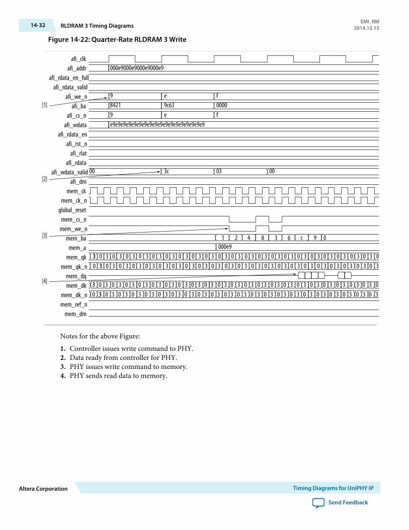
Figure 14-22: Quarter-Rate RLDRAM 3 Write
000e9000e9000e9000e9
e9c63e
f0000f
e9e9e9e9e9e9e9e9e9e9e9e9e9e9e9e9e9e9
3c 03 00
1 2 4 8 3 6 c 9 0
3 3 03 0 3 0 3 03 0 3 0 3 03 0 3 0 3 03 0 3 0 3 03 0 3 0 3 03 0 3 0 3 0 3
afi_clkafi_addr
afi_rdata_en_fullafi_rdata_valid
afi_we_nafi_ba
afi_cs_nafi_wdata
afi_rdata_enafi_rst_n
afi_rlatafi_rdata
afi_wdata_validafi_dm
mem_ckmem_ck_n
global_resetmem_cs_n
mem_we_nmem_ba
mem_amem_qk
mem_qk_nmem_dqmem_dk
mem_dk_nmem_ref_n
mem_dm
984219
0 3 0 3 03 3 03 0 3 0 3 03 0 3 0 3 03 0 3 0 3 03 0 3 0 3 03 0 3 0 3 03 0 3 0 3 0 3 0 3 0 30
3 3 03 0 3 0 3 03 0 3 0 3 03 0 3 0 3 03 0 3 0 3 03 0 3 0 3 03 0 3 0 3 0 3 0 3 0 3 03 3 03 0 3 0 3 03 0 3 0 3 03 0 3 0 3 03 0 3 0 3 03 0 3 0 3 03 0 3 0 3 0 3 0 3 0 30
00
000e9
[1]
[2]
[3]
[4]
Notes for the above Figure:
1. Controller issues write command to PHY.2. Data ready from controller for PHY.3. PHY issues write command to memory.4. PHY sends read data to memory.
14-32 RLDRAM 3 Timing DiagramsEMI_RM
2014.12.15
Altera Corporation Timing Diagrams for UniPHY IP
Send Feedback

Figure 14-23: Half-rate RLDRAM 3 Read
3
[1]
[2]
[3]
[4]
0... 0000800008003
3
00 21
1 0
63 003 0 2 39... 8888888888888888880 3 1 0300
000
xxxxxxxxx88... 888888888888888888
00009 000080 1 2 3 6 0
afi_clkafi_addr
afi_rdata_en_fullafi_rdata_valid
afi_we_nafi_ba
afi_cs_nafi_wdata
afi_rdata_enafi_rst_n
afi_rlatafi_rdata
afi_wdata_validafi_dm
mem_ckmem_ck_n
global_reset_nmem_cs_n
mem_we_nmem_a
mem_bamem_qk
mem_qk_nmem_dqmem_dk
mem_dk_nmem_ref_n
mem_dm
3 3 03 0 3 0 03 3 0 3 0 3 0 3 03 3 03 0 3 0 3 0 3 3 00 3 0 30
3 3 03 0 3 0 03 3 0 3 0 3 0 3 03 3 03 0 3 0 3 0 3 3 00 3 0 30
3 0 3 00 3 0 3
3 3 03 0 3 0 03 3 0 3 0 3 0 3 03 3 03 0 3 0 3 0 3 3 00 3 0 30
3 3 03 0 3 0 03 3 0 3 0 3 0 3 03 3 03 0 3 0 3 0 3 3 00 3 0 30
3 0 3 00 3 0 3
Notes for the above Figure:
1. Controller issues read command to PHY.2. PHY issues read command to memory.3. PHY receives data from memory.4. Controller receives read data from PHY.
EMI_RM2014.12.15 RLDRAM 3 Timing Diagrams 14-33
Timing Diagrams for UniPHY IP Altera Corporation
Send Feedback

Figure 14-24: Half-Rate RLDRAM 3 Write
afi_clkafi_addr
afi_rdata_en_fullafi_rdata_valid
afi_we_nafi_ba
afi_cs_nafi_wdata
afi_rdata_enafi_rst_n
afi_rlatafi_rdata
afi_wdata_validafi_dm
mem_ckmem_ck_n
global_reset_nmem_cs_n
mem_we_nmem_a
mem_bamem_qk
mem_qk_nmem_dqmem_dk
mem_dk_nmem_ref_n
mem_dmlocal_cal_success
0000700007003 1 3
21 63 003 1 37777777777777777770300fffffffffxxxxxxxxx0 c 000
00008 000070 1 2 3 6 03 3 03 0 3 0 3 0 3 0 3 0
3 3 03 0 3 0 3 3 00 303 3 03 0 3 0 3 0 3 0 3 0 3
3 3 03 0 3 0 3 3 00 3 00
3 3 03 0 3 0 3 0 3 0 3 03 3 03 0 3 0 3 3 00 30
3 3 03 0 3 0 3 0 3 0 3 0 33 3 03 0 3 0 3 3 00 3 00
[1]
[2]
[3]
[4]
Notes for the above Figure:
1. Controller issues write command to PHY.2. Data ready from controller for PHY.3. PHY issues write command to memory.4. PHY sends read data to memory.
Document Revision HistoryDate Version Changes
December2014
2014.12.15 Maintenance release.
August 2014 2014.08.15 Maintenance release.
December2013
2013.12.16 Updated timing diagrams for LPDDR2.
14-34 Document Revision HistoryEMI_RM
2014.12.15
Altera Corporation Timing Diagrams for UniPHY IP
Send Feedback

Date Version Changes
November2012
2.1 • Added timing diagrams for RLDRAM 3.• Changed chapter number from 10 to 12.
June 2012 2.0 • Added timing diagrams for LPDDR2.• Added Feedback icon.
November2011
1.1 • Consolidated timing diagrams from 11.0 DDR2 and DDR3 SDRAMController with UniPHY User Guide, QDR II and QDR II+ SRAMController with UniPHY User Guide, and RLDRAM II Controller withUniPHY IP User Guide.
• Added Read and Write diagrams for DDR3 quarter-rate.
EMI_RM2014.12.15 Document Revision History 14-35
Timing Diagrams for UniPHY IP Altera Corporation
Send Feedback

External Memory Interface Debug Toolkit 152014.12.15
EMI_RM Subscribe Send Feedback
The EMIF Toolkit lets you diagnose and debug calibration problems and produce margining reports foryour external memory interface.
The toolkit is compatible with UniPHY-based external memory interfaces that use the Nios II-basedsequencer, with toolkit communication enabled, and with Arria 10 EMIF IP. Toolkit communication ison by default in versions 10.1 and 11.0 of UniPHY IP; for version 11.1 and later, toolkit communication ison whenever debugging is enabled on the Diagnostics tab of the IP core interface.
The EMIF Toolkit can communicate with several different memory interfaces on the same device, but cancommunicate with only one memory device at a time.
Note: The EMIF Debug Toolkit does not support MAX 10 devices.
ArchitectureThe EMIF toolkit provides a graphical user interface for communication with connections.
All functions provided in the toolkit are also available directly from the quartus_sh TCL shell, throughthe external_memif_toolkit TCL package. The availablity of TCL support allows you to create scriptsto run automatically from TCL. You can find information about specific TCL commands by running help-pkg external_memif_toolkit from the quartus_sh TCL shell.
If you want, you can begin interacting with the toolkit through the GUI, and later automate yourworkflow by creating TCL scripts. The toolkit GUI records a history of the commands that you run. Youcan see the command history on the History tab in the toolkit GUI.
CommunicationCommunication between the EMIF Toolkit and external memory interface connections varies, dependingon the connection type and version. In versions 10.1 and 11.0 of the EMIF IP, communication is achievedusing direct communication to the Nios II-based sequencer. In version 11.1 and later, communication isachieved using a JTAG Avalon-MM master attached to the sequencer bus.
The following figure shows the structure of UniPHY-based IP version 11.1 and later, with JTAG Avalon-MM master attached to sequencer bus masters.
© 2014 Altera Corporation. All rights reserved. ALTERA, ARRIA, CYCLONE, ENPIRION, MAX, MEGACORE, NIOS, QUARTUS and STRATIX words and logos aretrademarks of Altera Corporation and registered in the U.S. Patent and Trademark Office and in other countries. All other words and logos identified astrademarks or service marks are the property of their respective holders as described at www.altera.com/common/legal.html. Altera warrants performanceof its semiconductor products to current specifications in accordance with Altera's standard warranty, but reserves the right to make changes to anyproducts and services at any time without notice. Altera assumes no responsibility or liability arising out of the application or use of any information,product, or service described herein except as expressly agreed to in writing by Altera. Altera customers are advised to obtain the latest version of devicespecifications before relying on any published information and before placing orders for products or services.
ISO9001:2008Registered
www.altera.com101 Innovation Drive, San Jose, CA 95134

Figure 15-1: UniPHY IP Version 11.1 and Later, with JTAG Avalon-MM Master
SCC PHY AFI Tracking
JTAG Avalon Master(new)
Combined ROM/RAM(Variable
Size )
Sequencer Managers
Bridge
NIOS II
Avalon -MM
Avalon-MM
Debug Bus
Sequencer Bus
Register File
EMIF Toolkit
Calibration and Report GenerationThe EMIF Toolkit uses calibration differently, depending on the version of external memory interface inuse. For versions 10.1 and 11.0 interfaces, the EMIF Toolkit causes the memory interface to calibrateseveral times, to produce the data from which the toolkit generates its reports. In version 11.1 and later,report data is generated during calibration, without need to repeat calibration. For version 11.1 and later,generated reports reflect the result of the previous calibration, without need to recalibrate unless youchoose to do so.
Setup and UseBefore using the EMIF Toolkit, you should compile your design and program the target device with theresulting SRAM Object File (. sof). For designs compiled in the Quartus II software version 12.0 or earlier,debugging information is contained in the JTAG Debugging Information file (.jdi); however, for designscompiled in the Quartus II software version 12.1 or later, all debugging information resides in the .sof file.
You can run the toolkit using all your project files, or using only the Quartus II Project File (.qpf),Quartus II Settings File (.qsf), and .sof file; the .jdi file is also required for designs compiled prior toversion 12.1. To ensure that all debugging information is correctly synchronized for designs compiledprior to version 12.1, ensure that the .sof and .jdi files that you used are generated during the same run ofthe Quartus II Assembler.
After you have programmed the target device, you can run the EMIF Toolkit and open your project. Youcan then use the toolkit to create connections to the external memory interface.
15-2 Calibration and Report GenerationEMI_RM
2014.12.15
Altera Corporation External Memory Interface Debug Toolkit
Send Feedback

General WorkflowTo use the EMIF Toolkit, you must link your compiled project to a device, and create a communicationchannel to the connection that you want to examine.
Linking the Project to a Device1. To launch the toolkit, select External Memory Interface Toolkit from the Tools menu in the Quartus II
software.2. After you have launched the toolkit, open your project and click the Initialize connections task in the
Tasks window, to initialize a list of all known connections.3. To link your project to a specific device on specific hardware, perform the following steps:
a. Click the Link Project to Device task in the Tasks window.b. Select the desired hardware from the Hardware dropdown menu in the Link Project to Device
dialog box.c. Select the desired device on the hardware from the Device dropdown menu in the Link Project to
Device dialog box.d. Select the correct Link file type, depending on the version of Quartus II software in which your
design was compiled:
• If your design was compiled in the Quartus II software version 12.0 or earlier, select JDI as theLink file type, verify that the .jdi file is correct for your .sof file, and click Ok.
• If your design was compiled in the Quartus II software version 12.1 or later, select SOF as theLink file type, verify that the .sof file is correct for your programmed device, and click Ok.
Figure 15-2: Link Project to Device Dialog Box
When you link your project to the device, the toolkit verifies all connections on the device against theinformation in the JDI or SOF file, as appropriate. If the toolkit detects any mismatch between the JDI fileand the device connections, an error message is displayed.
For designs compiled using the Quartus II software version 12.1 or later, the SOF file contains a designhash to ensure the SOF file used to program the device matches the SOF file specified for linking to aproject. If the hash does not match, an error message appears.
EMI_RM2014.12.15 General Workflow 15-3
External Memory Interface Debug Toolkit Altera Corporation
Send Feedback

If the toolkit successfully verifies all connections, it then attempts to determine the connection type foreach connection. Connections of a known type are listed in the Linked Connections report, and areavailable for the toolkit to use.
Establishing Communication to ConnectionsAfter you have completed linking the project, you can establish communication to the connections.
1. In the Tasks window,
• Click Establish Memory Interface Connection to create a connection to the external memoryinterface.
• Click Establish Efficiency Monitor Connection to create a connection to the efficiency monitor.2. To create a communication channel to a connection, select the desired connection from the displayed
pulldown menu of connections, and click Ok. The toolkit establishes a communication channel to theconnection, creates a report folder for the connection, and creates a folder of tasks for the connection.
Note: By default, the connection and the reports and tasks folders are named according to thehierarchy path of the connection. If you want, you can specify a different name for theconnection and its folders.
3. You can run any of the tasks in the folder for the connection; any resulting reports appear in thereports folder for the connection.
Selecting an Active InterfaceIf you have more than one external memory interface in an Arria 10 I/O column, you can select oneinstance as the active interface for debugging.
1. To select one of multiple EMIF instances in an Arria 10 I/O column, use the Set Active Interfacedialog box.
2. If you want to generate reports for the new active interface, you must first recalibrate the interface.
ReportsThe toolkit can generate a variety of reports, including summary, calibration, and margining reports forexternal memory interface connections. To generate a supported type of report for a connection, you runthe associated task in the tasks folder for that connection.
15-4 Establishing Communication to ConnectionsEMI_RM
2014.12.15
Altera Corporation External Memory Interface Debug Toolkit
Send Feedback

Summary Report
The Summary Report provides an overview of the memory interface; it consists of the following tables:
• Summary table. Provides a high-level summary of calibration results. This table lists details about theconnection, IP version, IP protocol, and basic calibration results, including calibration failures. Thistable also lists the estimated average read and write data valid windows, and the calibrated read andwrite latencies.
• Interface Details table. Provides details about the parameterization of the memory IP. This table allowsyou to verify that the parameters in use match the actual memory device in use.
• Groups Masked from Calibration table. Lists any groups that were masked from calibration whencalibration occurred. Masked groups are ignored during calibration.
Note: This table applies only to UniPHY-based interfaces; it is not applicable to Arria 10 EMIF.• Ranks Masked from Calibration tables (DDR2 and DDR3 only). Lists any ranks that were masked
from calibration when calibration occurred. Masked ranks are ignored during calibration.
Calibration Report (UniPHY)
The Calibration Report provides detailed information about the margins observed before and aftercalibration, and the settings applied to the memory interface during calibration; it consists of thefollowing tables:
• Per DQS Group Calibration table: Lists calibration results for each group. If a group fails calibration,this table also lists the reason for the failure.
Note: If a group fails calibration, the calibration routine skips all remaining groups. You candeactivate this behaviour by running the Enable Calibration for All Groups On Failurecommand in the toolkit.
• DQ Pin Margins Observed Before Calibration table: Lists the DQ pin margins observed before calibra‐tion occurs. You can refer to this table to see the per-bit skews resulting from the specific silicon andboard that you are using.
• DQS Group Margins Observed During Calibration table: Lists the DQS group margins observedduring calibration.
• DQ Pin Settings After Calibration and DQS Group Settings After Calibration table: Lists the settingsmade to all dynamically controllable parts of the memory interface as a result of calibration. You canrefer to this table to see the modifications made by the calibration algorithm.
Calibration Report (Arria 10 EMIF)
The Calibration Report provides detailed information about the margins observed before and aftercalibration, and the settings applied to the memory interface during calibration; it consists of thefollowing tables:
• Calibration Status Per Group table: Lists the pass/fail status per group.• DQ Pin Margins Observed During Calibration table: Lists the DQ read/write margins and calibrated
delay settings. These are the expected margins after calibration, based on calibration data patterns.This table also contains DM/DBI margins, if applicable.
• DQS Pin Margins Observed During Calibration table: Lists the DQS margins observed during calibra‐tion.
• FIFO Settings table: Lists the VFIFO and LFIFO settings made during calibration.• Latency Observed During Calibration table: Lists the calibrated read/write latency.• Address/Command Margins Observed During Calibration table: Lists the margins on calibrated A/C
pins, for protocols that support Address/Command calibration.
EMI_RM2014.12.15 Reports 15-5
External Memory Interface Debug Toolkit Altera Corporation
Send Feedback
Margin Report
The Margin Report lists the post-calibration margins for each DQ and data mask pin, keeping all otherpin settings constant; it consists of the following tables:
• DQ Pin Post Calibration Margins table. Lists the margin data in tabular format.• Read Data Valid Windows report. Shows read data valid windows in graphical format.• Write Data Valid Windows report. Shows write data valid windows in graphical format.
Note: The Margin Report applies only to UniPHY-based interfaces; it is not applicable to Arria 10 EMIF.For Arria 10 EMIF, the Calibration Report provides equivalent information.
Operational ConsiderationsSome features and considerations are of interest in particular situations.
Specifying a Particular JDI File
Correct operation of the EMIF Toolkit depends on the correct JDI being used when linking the project tothe device. The JDI file is produced by the Quartus II Assembler, and contains a list of all system leveldebug nodes and their heirarchy path names. If the default .jdi file name is incorrect for your project, youmust specify the correct .jdi file. The .jdi file is supplied during the link-project-to-device step, where therevision_name.jdi file in the project directory is used by default. To supply an alternative .jdi file, click onthe ellipse then select the correct .jdi file.
PLL Status
When connecting to DDR-based external memory interface connections, the PLL status appears in theEstablish Connection dialog box when the IP is generated to use the CSR controller port, allowing you toimmediately see whether the PLL status is locked. If the PLL is not locked, no communication can occuruntil the PLL becomes locked and the memory interface reset is deasserted.
When you are linking your project to a device, an error message will occur if the toolkit detects that aJTAG Avalon-MM master has no clock running. You can run the Reindex Connections task to have thetoolkit rescan for connections and update the status and type of found connections in the LinkedConnections report.
Margining Reports
The EMIF Toolkit can display margining information showing the post-calibration data-valid windowsfor reads and writes. Margining information is determined by individually modifying the input andoutput delay chains for each data and strobe/clock pin to determine the working region. The toolkit candisplay margining data in both tabular and hierarchial formats.
Group Masks
To aid in debugging your external memory interface, the EMIF Toolkit allows you to mask individualgroups and ranks from calibration. Masked groups and ranks are skipped during the calibration process,meaning that only unmasked groups and ranks are included in calibration. Subsequent mask operationsoverwrite any previous masks.
15-6 Operational ConsiderationsEMI_RM
2014.12.15
Altera Corporation External Memory Interface Debug Toolkit
Send Feedback

Using with Arria 10 Devices in a PHY-Only Configuration
If you want to use the Debug Toolkit with an Arria 10 EMIF IP in a PHY-only configuration, you mustconnect a debug clock and a reset signal to the Arria 10 external memory interface debug component.Altera recommends using the AFI clock and AFI reset for this purpose.
Note: For information about calibration stages in UniPHY-based interfaces, refer to UniPHY CalibrationStages in the Functional Description - UniPHY chapter. For information about calibration stages inArria 10 EMIF IP, refer to Arria 10 EMIF Calibration, in the Functional Description - Arria 10EMIF chapter.
Related Information
• Calibration Stages on page 1-54• Functional Description—UniPHY on page 1-1• Functional Description—Arria 10 EMIF on page 2-1
TroubleshootingIn the event of calibration failure, refer to the following figure to assist in troubleshooting your design.Calibration results and failing stages are available through the external memory interface toolkit.
Figure 15-3: Debugging Tips
Stage 1 Read Calibration
Guaranteed ReadFailure
Address/Command Skew Issue
Check Address/Command
Clock Phase
Check Address/Command
Board Skew and Delays
Ensure DQ and DQSare matched on the
board
Failing stage of group
Calibration Failure
DQ/DQS Centering Issue
Add or subtract delayto DQS to center DQS
within DQ window
Check DQS enable calibration margin
Check DQ-to-DQS phase; it should be edge aligned.
No working DQSenphase found
Ensure board parameters are correct and include
complete path to the memory device
Ensure board parametersare correct and include
complete path to thememory device
Per-bit Readdeskew failure
No first write levellingphase found
Verify the write levelingwindow to ensure allgroups are within the
maximum writeleveling range
Increase the D6delay on CLK Contact
Altera
No last working writeleveling phase found
Write leveling copyfailure
Stage 2 Write Leveling
Verify the write levelingwindow to ensure allgroups are within the
maximum writeleveling range
Increase the D6 delayon DQ and DQS for the
groups that cannotwrite level
LFIFO Tuning
Stage 3 Read Calibration
Failure is unexpected here.If a failure occurs at this
point, it is probablyStage 2 (Write Leveling)
that is failing.
Stage 4 WriteCalibration
Per-bit writedeskew
Mask the failing DQgroup and rerun
calibration
Check margins to seeif failure is all bits in
group or only some bits
Check DQ-to-DQS phase
Verify board tracesand solder joints
EMIF On-Chip Debug ToolkitThe EMIF On-Chip Debug Toolkit allows user logic to access the same calibration data used by the EMIFToolkit, and allows user logic to send commands to the sequencer. You can use the EMIF On-Chip DebugToolkit to access calibration data for your design and to send commands to the sequencer just as theEMIF Toolkit would. The following information is available:
EMI_RM2014.12.15 Troubleshooting 15-7
External Memory Interface Debug Toolkit Altera Corporation
Send Feedback

• Pass/fail status for each DQS group• Read and write data valid windows for each group
In addition, user logic can request the following commands from the sequencer:
• Destructive recalibration of all groups• Masking of groups and ranks• Generation of per-DQ pin margining data as part of calibration
The user logic communicates through an Avalon-MM slave interface as shown below.
Figure 15-4: User Logic Access
User logicAltera
Memory InterfaceAvalon Slave
Note: The memory map for Arria 10 On-Chip Debug will be made available in a future release.
Access ProtocolThe EMIF On-Chip Debug Toolkit provides access to calibration data through an Avalon-MM slaveinterface. To send a command to the sequencer, user logic sends a command code to the command spacein sequencer memory. The sequencer polls the command space for new commands after each groupcompletes calibration, and continuously after overall calibration has completed.
The communication protocol to send commands from user logic to the sequencer uses a multistephandshake with a data structure as shown below, and an algorithm as shown in the figure which follows.
typedef struct_debug_data_struct {...// Command interactionalt_u32 requested_command;alt_u32 command_status;alt_u32 command_parameters[COMMAND_PARAM_WORDS];...}
To send a command to the sequencer, user logic must first poll the command_status word for a value ofTCLDBG_TX_STATUS_CMD_READY, which indicates that the sequencer is ready to accept commands. Whenthe sequencer is ready to accept commands, user logic must write the command parameters intocommand_parameters, and then write the command code into requested_command.
The sequencer detects the command code and replaces command_status withTCLDBG_TX_STATUS_CMD_EXE, to indicate that it is processing the command. When the sequencer hasfinished running the command, it sets command_status to TCLDBG_TX_STATUS_RESPONSE_READY toindicate that the result of the command is available to be read. (If the sequencer rejects the requestedcommand as illegal, it sets command_status to TCLDBG_TX_STATUS_ILLEGAL_CMD.)
User logic acknowledges completion of the command by writing TCLDBG_CMD_RESPONSE_ACK torequested_command. The sequencer responds by setting command_status back to STATUS_CMD_READY. (Ifan illegal command is received, it must be cleared using CMD_RESPONSE_ACK.)
15-8 Access ProtocolEMI_RM
2014.12.15
Altera Corporation External Memory Interface Debug Toolkit
Send Feedback

Figure 15-5: Debugging Algorithm Flowchart
Read Command_status
Yes
Nocommand_status == CMD_READY ?
End
Yes
Nocommand_status == RESPONSE_READY ?
Write command payload
Write command code
Read command_status
Write RESPONSE_ACK code
Command Codes ReferenceThe following table lists the supported command codes for the On-Chip Debug Toolkit.
Table 15-1: Supported Command Codes
Command Parameters Description
TCLDBG_RUN_MEM_CALIBRATE None Runs the calibration routine.
TCLDBG_MARK_ALL_DQS_GROUPS_AS_VALID
None Marks all groups as valid forcalibration.
TCLDBG_MARK_GROUP_AS_SKIP Group to skip Mark the specified group to beskipped by calibration.
EMI_RM2014.12.15 Command Codes Reference 15-9
External Memory Interface Debug Toolkit Altera Corporation
Send Feedback

Command Parameters Description
TCLDBG_MARK_ALL_RANKS_AS_VALID None Mark all ranks as valid for calibra‐tion
TCLDBG_MARK_RANK_AS_SKIP Rank to skip Mark the specified rank to beskipped by calibration.
TCLDBG_ENABLE_MARGIN_REPORT None Enables generation of the marginreport.
Header FilesThe external memory interface IP generates header files which identify the debug data structures andmemory locations used with the EMIF On-Chip Debug Toolkit. You should refer to these header files forinformation required for use with your core user logic. It is highly recommended to use a softwarecomponent (such as a Nios II processor) to access the calibration debug data.
The header files are unique to your IP parameterization and version, therefore you must ensure that youare referring to the correct version of header for your design. The names of the header files are:core_debug.h and core_debug_defines.h. (Arria 10 header files will be available in a future release.)
Generating IP With the Debug PortThe following steps summarize the procedure for implementing your IP with the EMIF On-Chip DebugToolkit enabled.
1. Start the Quartus II software and generate a new external memory interface. For QDR II andRLDRAM II protocols, ensure that sequencer optimization is set to Performance (for Nios II-basedsequencer).
2. On the Diagnostics tab of the parameter editor, turn on Enable EMIF On-Chip Debug Toolkit.3. Ensure that the EMIF On-Chip Debug Toolkit interface type is set to Avalon-MM Slave.4. Click Finish to generate your IP.5. Find the Avalon interface in the top-level generated file. Connect this interface to your debug
component.
input wire [19:0] seq_debug_addr, // seq_debug.addressinput wire seq_debug_read_req, // .readoutput wire [31:0] seq_debug_rdata, // .readdatainput wire seq_debug_write_req, // .writeinput wire [31:0] seq_debug_wdata, // .writedataoutput wire seq_debug_waitrequest, // .waitrequestinput wire [3:0] seq_debug_be, // .byteenableoutput wire seq_debug_rdata_valid // .readdatavalid
If you are using UniPHY-based IP with the hard memory controller, also connect the seq_debug_clkand seq_debug_reset_in signals to clock and asynchronous reset signals that control your debuglogic.
6. Find the core_debug.h and core_debug_defines.h header files in <design_name>/<design_name>_s0_software and include these files in your debug component code.
7. Write your debug component using the supported command codes, to read and write to the Avalon-MM interface.
15-10 Header FilesEMI_RM
2014.12.15
Altera Corporation External Memory Interface Debug Toolkit
Send Feedback

The debug data structure resides at the memory address SEQ_CORE_DEBUG_BASE, which is defined in thecore_debug_defines.h header file.
Note: Arria 10 header files will be made available in a future release.
Example C Code for Accessing Debug DataA typical use of the EMIF On-Chip Debug Toolkit might be to recalibrate the external memory interface,and then access the reports directly using the summary_report_ptr, cal_report_ptr, andmargin_report_ptr pointers, which are part of the debug data structure.
The following code sample illustrates:
/* * DDR3 UniPHY sequencer core access example*/
#include <stdio.h>#include <unistd.h>#include <io.h>#include "core_debug_defines.h"
int send_command(volatile debug_data_t* debug_data_ptr, int command, int args[], int num_args){volatile int i, response;
// Wait until command_status is readydo { response = IORD_32DIRECT(&(debug_data_ptr->command_status), 0);} while(response != TCLDBG_TX_STATUS_CMD_READY);
// Load argumentsif(num_args > COMMAND_PARAM_WORDS){// Too many argumentsreturn 0;}for(i = 0; i < num_args; i++){IOWR_32DIRECT(&(debug_data_ptr->command_parameters[i]), 0, args[i]);}// Send command codeIOWR_32DIRECT(&(debug_data_ptr->requested_command), 0, command);// Wait for acknowledgmentdo { response = IORD_32DIRECT(&(debug_data_ptr->command_status), 0);} while(response != TCLDBG_TX_STATUS_RESPOSE_READY && response != TCLDBG_TX_STATUS_ILLEGAL_CMD);// Acknowledge responseIOWR_32DIRECT(&(debug_data_ptr->requested_command), 0, TCLDBG_CMD_RESPONSE_ACK);// Return 1 on success, 0 on illegal commandreturn (response != TCLDBG_TX_STATUS_ILLEGAL_CMD);}int main(){ volatile debug_data_t* my_debug_data_ptr; volatile debug_summary_report_t* my_summary_report_ptr; volatile debug_cal_report_t* my_cal_report_ptr; volatile debug_margin_report_t* my_margin_report_ptr;volatile debug_cal_observed_dq_margins_t* cal_observed_dq_margins_ptr; int i, j, size; int args[COMMAND_PARAM_WORDS]; // Initialize pointers to the debug reports my_debug_data_ptr = (debug_data_t*)SEQ_CORE_DEBUG_BASE;
EMI_RM2014.12.15 Example C Code for Accessing Debug Data 15-11
External Memory Interface Debug Toolkit Altera Corporation
Send Feedback

my_summary_report_ptr = (debug_summary_report_t*)(IORD_32DIRECT(&(my_debug_data_ptr->summary_report_ptr), 0)); my_cal_report_ptr = (debug_cal_report_t*)(IORD_32DIRECT(&(my_debug_data_ptr->cal_report_ptr), 0)); my_margin_report_ptr = (debug_margin_report_t*)(IORD_32DIRECT(&(my_debug_data_ptr->margin_report_ptr), 0));
// Activate all groups and ranks send_command(my_debug_data_ptr, TCLDBG_MARK_ALL_DQS_GROUPS_AS_VALID, 0, 0); send_command(my_debug_data_ptr, TCLDBG_MARK_ALL_RANKS_AS_VALID, 0, 0); send_command(my_debug_data_ptr, TCLDBG_ENABLE_MARGIN_REPORT, 0, 0);
// Mask group 4args[0] = 4; send_command(my_debug_data_ptr, TCLDBG_MARK_GROUP_AS_SKIP, args, 1); send_command(my_debug_data_ptr, TCLDBG_RUN_MEM_CALIBRATE, 0, 0);
// SUMMARY printf("SUMMARY REPORT\n"); printf("mem_address_width: %u\n", IORD_32DIRECT(&(my_summary_report_ptr->mem_address_width), 0)); printf("mem_bank_width: %u\n", IORD_32DIRECT(&(my_summary_report_ptr->mem_bank_width), 0)); // etc...
// CAL REPORT printf("CALIBRATION REPORT\n"); // DQ read margins for(i = 0; i < RW_MGR_MEM_DATA_WIDTH; i++) { cal_observed_dq_margins_ptr = &(my_cal_report_ptr->cal_dq_in_margins[i]); printf("0x%x DQ %d Read Margin (taps): -%d : %d\n", (unsigned int)cal_observed_dq_margins_ptr, i, IORD_32DIRECT(&(cal_observed_dq_margins_ptr->left_edge), 0), IORD_32DIRECT(&(cal_observed_dq_margins_ptr->right_edge), 0)); } // etc... return 0;}
Debug Report for Arria V and Cyclone V SoC DevicesThe External Memory Interface Debug Toolkit and EMIF On-Chip Debug Toolkit do not work with ArriaV and Cyclone V SoC devices. Debugging information for Arria V and Cyclone V SoC devices is availableby enabling a debug output report, which contains similar information.
Enabling the Debug Report for Arria V and Cyclone V SoC DevicesTo enable a debug report for Arria V or Cyclone V SoC devices, perform the following steps:
1. Open the <design_name>/hps_isw_handoff/sequencer_defines.h file in a text editor.2. In the sequencer_defines.h file, locate the following line: #define RUNTIME_CAL_REPORT 03. Change #define RUNTIME_CAL_REPORT 0 to #define RUNTIME_CAL_REPORT 1, and save the file.4. Generate the board support package (BSP) with semihosting enabled, or with UART output.
The system will now generate the debugging report as part of the calibration process.
Document Revision History
15-12 Debug Report for Arria V and Cyclone V SoC DevicesEMI_RM
2014.12.15
Altera Corporation External Memory Interface Debug Toolkit
Send Feedback

Date Version Changes
December2014
2014.12.15 • Added paragraph to step 5 of Generating IP With the Debug Port.• Added mention of seq_debug_clk and seq_debug_reset_in to step
5 of Generating IP With the Debug Port.
August 2014 2014.08.15 Maintenance release.
December2013
2013.12.16 Maintenance release.
November2012
2.2 • Changes to Setup and Use and General Workflow sections.• Added EMIF On-Chip Debug Toolkit section• Changed chapter number from 11 to 13.
August 2012 2.1 Added table of debugging tips.
June 2012 2.0 • Revised content for new UnIPHY EMIF Toolkit.• Added Feedback icon.
November2011
1.0 Harvested 11.0 DDR2 and DDR3 SDRAM Controller with UniPHY EMIFToolkit content.
EMI_RM2014.12.15 Document Revision History 15-13
External Memory Interface Debug Toolkit Altera Corporation
Send Feedback

Upgrading to UniPHY-based Controllers fromALTMEMPHY-based Controllers 16
2014.12.15
EMI_RM Subscribe Send Feedback
The following topics describe the process of upgrading to UniPHY from DDR2 or DDR3 SDRAM High-Performance Controller II with ALTMEMPHY Designs.
NOTE: Designs that do not use the AFI cannot be upgraded to UniPHY. If your design uses non-AFI IPcores, Altera recommends that you start a new design with the UniPHY IP core . In addition, Alterarecommends that any new designs targeting Stratix III, Stratix IV, or Stratix V use the UniPHY datapath.
To upgrade your ALTMEMPHY-based DDR2 or DDR3 SDRAM High-Performance Controller II designto a DDR2 or DDR3 SDRAM controller with UniPHY IP core, you must complete the tasks listed below:
1. Generating Equivalent Design2. Replacing the ALTMEMPHY Datapath with UniPHY Datapath3. Resolving Port Name Differences4. Creating OCT Signals5. Running Pin Assignments Script6. Removing Obsolete Files7. Simulating your Design
The following topics describe these tasks in detail.
Related Information
• Generating Equivalent Design on page 16-1• Replacing the ALTMEMPHY Datapath with UniPHY Datapath on page 16-2• Resolving Port Name Differences on page 16-2• Creating OCT Signals on page 16-4• Running Pin Assignments Script on page 16-4• Removing Obsolete Files on page 16-4• Simulating your Design on page 16-4• Creating OCT Signals on page 16-4
Generating Equivalent DesignCreate a new DDR2 or DDR3 SDRAM controller with UniPHY IP core, by following the steps inImplementing and Parameterizing Memory IP and apply the following guidelines:
© 2014 Altera Corporation. All rights reserved. ALTERA, ARRIA, CYCLONE, ENPIRION, MAX, MEGACORE, NIOS, QUARTUS and STRATIX words and logos aretrademarks of Altera Corporation and registered in the U.S. Patent and Trademark Office and in other countries. All other words and logos identified astrademarks or service marks are the property of their respective holders as described at www.altera.com/common/legal.html. Altera warrants performanceof its semiconductor products to current specifications in accordance with Altera's standard warranty, but reserves the right to make changes to anyproducts and services at any time without notice. Altera assumes no responsibility or liability arising out of the application or use of any information,product, or service described herein except as expressly agreed to in writing by Altera. Altera customers are advised to obtain the latest version of devicespecifications before relying on any published information and before placing orders for products or services.
ISO9001:2008Registered
www.altera.com101 Innovation Drive, San Jose, CA 95134

• Specify the same variation name as the ALTMEMPHY variation.• Specify a directory different than the ALTMEMPHY design directory to prevent files from overwriting
each other during generation.
To ease the migration process, ensure the UniPHY-based design you create is as similar as possible to theexisting ALTMEMPHY-based design. In particular, you should ensure the following settings are the samein your UniPHY-based design:
• PHY settings tab• FPGA speed grade• PLL reference clock• Memory clock frequency• There is no need to change the default Address and command clock phase settings; however, if you
have board skew effects in your ALTMEMPHY design, enter the difference between that clock phaseand the default clock phase into the Address and command clock phase settings.
• Memory Parameters tab—all parameters must match.• Memory Timing tab—all parameters must match.• Board settings tab—all parameters must match.• Controller settings tab—all parameters must match
Note: In ALTMEMPHY-based designs you can turn off dynamic OCT. However, all UniPHY-baseddesigns use dynamic parallel OCT and you cannot turn it off.
Related InformationImplementing and Parameterizing Memory IP
Replacing the ALTMEMPHY Datapath with UniPHY DatapathTo replace the ALTMEMPHY datapath with the UniPHY datapath, follow these steps:
1. In the Quartus II software, open the Assignment Editor, on the Assignments menu click AssignmentEditor.
2. Manually, delete all of the assignments related to the external memory interface pins, except for thelocation assignments if you are preserving the pinout. By default, these pin names start with the memprefix, though in your design they may have a different name.
3. Remove the old ALTMEMPHY .qip file from the project, as follows:
a. On the Assignments menu click Settings.b. Specify the old .qip, and click Remove.
Your design now uses the UniPHY datapath.
Resolving Port Name DifferencesSeveral port names in the ALTMEMPHY datapath are different than in the UniPHY datapath. Thedifferent names may cause compilation errors.
This topic describes the changes you must make in the RTL for the entity that instantiates the memory IPcore. Each change applies to a specific port in the ALTMEMPHY datapath. Unconnected ports require nochanges.
In some instances, multiple ports in ALTMEMPHY-based designs are mapped to a single port inUniPHY-based designs. If you use both ports in ALTMEMPHY-based designs, assign a temporary signal
16-2 Replacing the ALTMEMPHY Datapath with UniPHY DatapathEMI_RM
2014.12.15
Altera Corporation Upgrading to UniPHY-based Controllers from ALTMEMPHY-based Controllers
Send Feedback

to the common port and connect it to the original wires. The following table shows the changes you mustmake.
Table 16-1: Changes to ALTMEMPHY Port Names
ALTMEMPHY Port Changes
aux_full_rate_clk The UniPHY-based design does not generate this signal. You can generate itif you require it.
aux_scan_clk The UniPHY-based design does not generate this signal. You can generate itif you require it.
aux_scan_clk_reset_n The UniPHY-based design does not generate this signal. You can generate itif you require it.
dll_reference_clk The UniPHY-based design does not generate this signal. You can generate itif you require it.
dqs_delay_ctrl_export This signal is for DLL sharing between ALTMEMPHY instances and is notapplicable for UniPHY-based designs.
local_address Rename to avl_addr.
local_be Rename to avl_be.
local_burstbegin Rename to avl_burstbegin.
local_rdata Rename to avl_rdata.
local_rdata_valid Rename to avl_rdata_valid.
local_read_req Rename to avl_read_req.
local_ready Rename to avl_ready.
local_size Rename to avl_size.
local_wdata Rename to avl_wdata.
local_write_req Rename to avl_write_req.
mem_addr Rename to mem_a.
mem_clk Rename to mem_ck.
mem_clk_n Rename to mem_ck_n.
mem_dqsn Rename to mem_dqs_n.
EMI_RM2014.12.15 Resolving Port Name Differences 16-3
Upgrading to UniPHY-based Controllers from ALTMEMPHY-based Controllers Altera Corporation
Send Feedback

ALTMEMPHY Port Changes
oct_ctl_rs_value Remove from design (see “Creating OCT Signals”).
oct_ctl_rt_value Remove from design (see “Creating OCT Signals”).
phy_clk Rename to afi_clk.
reset_phy_clk_n Rename to afi_reset_n.
local_refresh_ack
reset_request_nThe controller no longer exposes these signals to the top-level design, socomment out these outputs. If you need it, bring the wire out from the high-performance II controller entity in <project_directory>/<variation name>.v.
Related InformationCreating OCT Signals on page 16-4
Creating OCT SignalsIn ALTMEMPHY-based designs, the Quartus II Fitter creates the alt_oct block outside the IP core andconnects it to the oct_ctl_rs_value and oct_ctl_rt_value signals.
In UniPHY-based designs, the OCT block is part of the IP core, so the design no longer requires these twoports. Instead, the UniPHY-based design requires two additional ports, oct_rup and oct_rdn (for StratixIII and Stratix IV devices), or oct_rzqin (for Stratix V devices). You must create these ports in theinstantiating entity as input pins and connect to the UniPHY instance. Then route these pins to the top-level design and connect to the OCT RUP and RDOWN resistors on the board.
For information on OCT control block sharing, refer to “The OCT Sharing Interface” in this volume.
Running Pin Assignments ScriptRemap your design by running analysis and synthesis.
When analysis and synthesis completes, run the pin assignments Tcl script and then verify the new pinassignments in the Assignment Editor.
Removing Obsolete FilesAfter you upgrade the design, you may remove the unnecessary ALTMEMPHY design files from yourproject.
To identify these files, examine the original ALTMEMPHY-generated .qip file in any text editor.
Simulating your DesignYou must use the UniPHY memory model to simulate your new design.
16-4 Creating OCT SignalsEMI_RM
2014.12.15
Altera Corporation Upgrading to UniPHY-based Controllers from ALTMEMPHY-based Controllers
Send Feedback

To use the UniPHY memory model, follow these steps:
1. Edit your instantiation of the UniPHY datapath to ensure the local_init_done, local_cal_success,local_cal_fail, soft_reset_n, oct_rdn, oct_rup, reset_phy_clk_n, and phy_clk signals are atthe top-level entity so that an instantiating testbench can refer to those signals.
2. To use the UniPHY testbench and memory model, generate the example design when generating yourIP instantiation.
3. Specify that your third-party simulator should use the UniPHY testbench and memory model insteadof the ALTMEMPHY memory model, as follows:
a. On the Assignments menu, point to Settings and click the Project Settings window.b. Select the Simulation tab, click Test Benches, click Edit, and replace the ALTMEMPHY testbench
files with the following files:
• \<project directory>\<variation name>_example_design\simulation\verilog\submodules\altera_avalon_clock_source.sv or \<project directory>\<variation name>_example_design\simulation\vhdl\submodules\altera_avalon_clock_source.vhd
• \<project directory>\<variation name>_example_design\simulation\verilog\submodules\altera_avalon_reset_source.sv or \<project directory>\<variation name>_example_design\simulation\vhdl\submodules\altera_avalon_reset_source.vhd
• \<project directory>\<variation name>_example_design\simulation\verilog\<variation name>_example_sim.v or \uniphy\<variation name>_example_design\simulation\vhdl\<variation name>_example_sim.vhd
• \<project directory>\<variation name>_example_design\simulation\verilog\submodules\verbosity_pkg.sv
• \<project directory>\<variation name>_example_design\simulation\verilog\submodules\status_checker_no_ifdef_params.sv or \<project directory>\<variation name>_example_design\simulation\vhdl\submodules\status_checker_no_ifdef_params.sv
• \<project directory>\<variation name>_example_design\simulation\verilog\submodules\alt_mem_if_common_ddr_mem_model_ddr3_mem_if_dm_pins_en_mem_if_dqsn_en.sv or \<project directory>\<variation name>_example_design\simulation\vhdl\submodules\alt_mem_if_common_ddr_mem_model_ddr3_mem_if_dm_pins_en_mem_if_dqsn_en.sv
• \<project directory>\<variation name>_example_design\simulation\verilog\submodules\alt_mem_if_ddr3_mem_model_top_ddr3_mem_if_dm_pins_en_mem_if_dqsn_en or \<project directory>\<variationname>_example_design\simulation\vhdl\submodules\alt_mem_if_ddr3_mem_model_top_ddr3_mem_if_dm_pins_en_mem_if_dqsn_en
4. Open the <variation name>_example_sim.v file and find the UniPHY-generated simulation exampledesign module name below: <variation name>_example_sim_e0.
5. Change the module name above to the name of your top-level design module.6. Refer to the following table and update the listed port names of the example design in the UniPHY-
generated <variation name>_example_sim.v file.
Table 16-2: Example Design Port Names
Example Design Name New Name
pll_ref_clk Rename to clock_source.
mem_a Rename to mem_addr.
mem_ck Rename to mem_clk.
EMI_RM2014.12.15 Simulating your Design 16-5
Upgrading to UniPHY-based Controllers from ALTMEMPHY-based Controllers Altera Corporation
Send Feedback

Example Design Name New Name
mem_ck_n Rename to mem_clk_n.
mem_dqs_n Rename to mem_dqsn.
drv_status_pass Rename to pnf.
afi_clk Rename to phy_clk.
afi_reset_n Rename to reset_phy_clk_n.
drv_status_fail This signal is not available, so comment out thisoutput.
afi_half_clk This signal is not exposed to the top-level design, socomment out this output.
For more information about generating example simulation files, refer to Simulating Memory IP, involume 2 of the External Memory Interface Handbook.
Document Revision HistoryDate Version Changes
December2014
2014.12.15 Maintenance release.
August 2014 2014.08.15 Maintenance release.
December2013
2013.12.16 Removed local_wdata_req from port names table.
November2012
2.3 Changed chapter number from 12 to 14.
June 2012 2.2 Added Feedback icon.
November2011
2.1 Revised Simulating your Design section.
16-6 Document Revision HistoryEMI_RM
2014.12.15
Altera Corporation Upgrading to UniPHY-based Controllers from ALTMEMPHY-based Controllers
Send Feedback