fabrication and characterization of graphene field effect ... · fabrication and characterization...
TRANSCRIPT
Fabrication and Characterization of
Graphene Field Effect Transistors
Sam Vaziri
Master Thesis in
Integrated Devices and Circuits Royal Institute of Technology (KTH)
Supervised By
Dr. Max Lemme
Examiner:
Prof. Mikael Östling
June, 2011
II
Abstract
Exceptional electronic properties of graphene have attracted the attention of solid-state
physicists and more recently device engineers. From electronic device point of view, graphene
is a promising material for future smaller and faster electronics, and it demands extensive
amount of research. In this work, graphene is used as the channel material in field effect
transistors (FETs). First KTH’s back-gate and top-gate graphene FETs (GFETs) were fabricated
using exfoliated graphene on 90 nm thick silicon dioxide films on silicon substrates. Aluminum
Oxide (Al2O3) high-K gate insulator was deposited by atomic layer deposition (ALD).
Back-gate transfer characteristics of uncovered devices show current modulation with
hysteresis and a charge neutrality point about +5 V. After 20 nm thick Al2O3 film deposition,
hysteresis is effectively suppressed, and the charge neutrality point moves toward negative
gate voltages of about -14 V. Furthermore, the mobility is just degraded by a factor of two after
high-k deposition process. The electrical characterization confirmed the effectiveness of the
fabrication and reveals the importance of contact optimization for device performance and
mobility extraction.

III
To my dearly loved wife, Negar
IV
Acknowledgement
I am deeply grateful to my supervisor, Dr. Max Lemme, for his kind guidance and excellent
supervision. His knowledge and expertise in the field of device technology and especially
graphene devices added considerably to my graduate experience. I would really like to
appreciate his invaluable help and friendship.
I am heartily thankful to Professor Mikael Östling for his support, ideas, and guidance from
inception of my master project here at KTH. Also, I am indebted to him since he helped me to
find my field of interest in device technology.
I would like to express my deep gratitude to Professor Carl-Mikael Zetterling for his useful
courses, and also his support during these two years of master program. I am thankful to Dr.
Gunnar Malm for his valuable help in characterization part, Dr. Per-Eric Hellström for his kind
support and guidance in the fabrication part, Dr. Anand Srinivasan and Reza Sanatinia for
Raman Spectroscopy, and also Dr. Henry Radamson for his supports.
Many Thanks are given to my friend Arash Salemi for all his help during this master program.
Special thanks to Valur Gudmundsson, Reza Ghandi, and Christoph Henkel for their help and
guidance during this project. I also want to appreciate Maziar Manouchehri’s help and fruitful
discussions.
I am thankful to Majid Mohseni, Mohammadreza Kolahdouz, Sohrab Redjai, Oscar Gustafsson,
Luigia Lanni, Benedetto Buono, and Eugenio Dentoni Litta for the encouragement and supports.
I thank my family for all supports and inspiration they have been giving me for all my life.
Especially I wish to express my deep love and gratitude to my wife, Negar, for her support and
companionship during all these years.
V
Table of Contents
Abstract .................................................................................................................................................. II
Acknowledgement ................................................................................................................................. IV
1. Introduction .................................................................................................................................... 1
2. Graphene......................................................................................................................................... 3
2.1. Graphene Properties ................................................................................................................ 3
2.2. Graphene Applications ............................................................................................................. 5
2.3. Graphene Production Methods ................................................................................................ 6
2.3.1. Mechanical exfoliation ..................................................................................................... 6
2.3.2. Epitaxial Growth on Silicon Carbide Single Crystal ............................................................. 7
2.3.3. Chemical Vapour Deposition............................................................................................. 7
2.3.4. Self Assembly of Soluble graphene ................................................................................... 7
2.4. Graphene field effect transistors .............................................................................................. 7
2.4.1. Mobility Degradation in GFETs .......................................................................................... 8
2.4.2. Current-Voltage Characterics of GFETs ............................................................................. 9
3. Fabrication .................................................................................................................................... 11
3.1. Graphene Production ............................................................................................................. 11
3.1.1. Substrate preparation .................................................................................................... 11
3.1.2. Graphene production and transfer ................................................................................. 12
3.2. Device Fabrication .................................................................................................................. 13
3.2.1. Design ............................................................................................................................ 14
3.2.2. E-beam Lithography (EBL) ............................................................................................... 15
3.2.3. Source and Drain Metal Contacts .................................................................................... 15
3.2.4. High k material deposition using ALD .............................................................................. 16
3.2.5. Gate Electrode................................................................................................................ 18
3.3. Summary ............................................................................................................................... 19
4. Characterization ............................................................................................................................ 20
4.1. Raman Spectroscopy .............................................................................................................. 20
4.2. Characterization of Back-gate Devices .................................................................................... 22
4.2.1. Uncovered Back-gate GFETs ........................................................................................... 24
4.2.2. Back-gated GFETs with Al2O3 top layer ............................................................................ 27
VI
4.3. Mobility Extraction: Limits and challenges .............................................................................. 29
4.3.1. Series resistance ............................................................................................................. 29
4.3.2. Back gate devices with Back contact ............................................................................... 33
4.4. Characterization of top-gate devices ...................................................................................... 34
5. Conclusion ..................................................................................................................................... 36
References ............................................................................................................................................ 38
1
1. Introduction
For almost half a century industry has fulfilled Moor’s Law by subsequent transistor
downscaling to have faster and cheaper Integrated Circuits (ICs), while consuming fewer
resources. However, as the physical limits of this downscaling are finally approached, extensive
research is being carried out on alternative materials and novel designs to sustain such
development. Materials with higher mobility and the ability to be downscaled beyond silicon
have attracted an extensive amount of research. As an outstanding example, the superior
electrical properties of recently discovered two-dimensional graphene [1] make it a promising
candidate for replacement of channel material in conventional field effect transistors [2].
From the isolation of real two-dimensional carbon sheet graphene in 2004, its outstanding
electrical and mechanical properties have been experimentally shown. Properties, production
methods, and applications of graphene are briefly discussed in chapter two. Among its
characteristics, three specific ones make it very unique among other candidates for future
faster and smaller electronics. The first and maybe the most important priority of graphene is
its ultrahigh intrinsic mobility. It has been shown that graphene’s upper mobility limit at room
temperature is absolutely higher than silicon and any other material at this time [3] .The next
advantage is the fact that graphene is thermodynamically stable in 2-D which makes it an ideal
material as the channel material in case of gate control in integrated circuits technology [4].
Finally the compatibility of graphene with standard silicon technology [5] makes it easy and
cost-effective to integrate with existing CMOS fabrication plants. Yet, having no band gap
results in poor on-off ratio in graphene field effect transistors and its application in logic circuits
is not expected for near future. On the other hand, other electronic applications like
radiofrequency transistors can benefit the ultrafast carrier transport in graphene. So,
maintaining the high intrinsic mobility along device fabrication is crucial.
2
Thus, when graphene comes into application its great electrical qualities downgrade
significantly. One of the main issues is the mobility degradation because of poor
graphene/insulator interface. Consequently, a proper gate dielectric material, and optimized
deposition method is required to decrease the effect of fabrication process in device
performance. Thanks to the mature MOSFET technology, using a high-k material has the priority
of higher screening effect and also higher gate control. Yet, high-k deposition on graphene is
still challenging, since it introduces charge impurities into the graphene and graphene/high-k
interface respectively. Al2O3 is one of the widely used high-k gate materials in graphene
transistors. Also, it has been shown that among deposition methods atomic layer deposition
(ALD) results in less introduced defects and higher dielectric quality [6]. But Al2O3 cannot be
directly deposited on graphene and we applied a specific method of using a nucleation layer
[7]. In this project, complete fabrication process was carried out and resulted in the first KTH’s
graphene back-gate and top-gate transistors. The fabrication process flow is described in
chapter three.
Chapter 4 is devoted to characterization and discussion over the results to investigate the
effectiveness of fabrication process, and transport characteristics in our devices. In fact,
characterization plays an important role in monitoring various fabrication steps and device
study. For instance, while Raman spectroscopy is reliable tool for identification of graphene
layers and quality, current-voltage measurements provide valuable data for extraction of
electrical parameters like mobility. This project aims to be an accomplishment guide for design,
fabrication, and characterization of back-gate and top-gate field effect transistors using high-k
top-gate dielectric.
3
2. Graphene
From more than fifty years ago, graphene had been predicted theoretically [8]. However,
it took quite long for scientist to make a 2-D material in 3-D nature. Graphene’s odd
dimensionality brings excellent properties and novel applications. This chapter briefly describes
graphene’s properties, applications, production methods, and transistors.
2.1. Graphene Properties
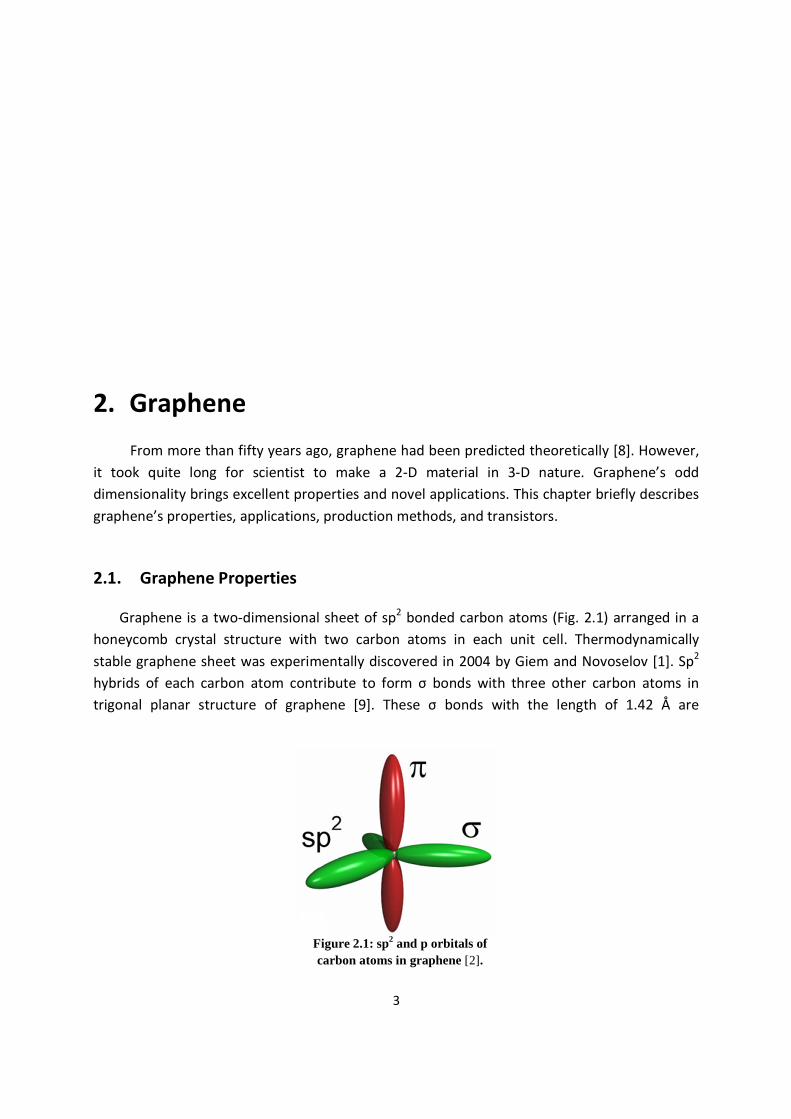
Graphene is a two-dimensional sheet of sp2 bonded carbon atoms (Fig. 2.1) arranged in a
honeycomb crystal structure with two carbon atoms in each unit cell. Thermodynamically
stable graphene sheet was experimentally discovered in 2004 by Giem and Novoselov [1]. Sp2
hybrids of each carbon atom contribute to form σ bonds with three other carbon atoms in
trigonal planar structure of graphene [9]. These σ bonds with the length of 1.42 Å are
Figure 2.1: sp2 and p orbitals of carbon atoms in graphene [2].
4
responsible for mechanical properties of graphene. The p orbitals of adjacent carbon atoms are
normal to the planar structure, and can bind to form a half-filled π band which gives rise to
graphene’s unique electronic properties.
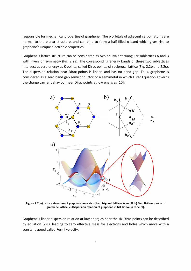
Graphene’s lattice structure can be considered as two equivalent triangular sublattices A and B
with inversion symmetry (Fig. 2.2a). The corresponding energy bands of these two sublattices
intersect at zero energy at K points, called Dirac points, of reciprocal lattice (Fig. 2.2b and 2.2c).
The dispersion relation near Dirac points is linear, and has no band gap. Thus, graphene is
considered as a zero band gap semiconductor or a semimetal in which Dirac Equation governs
the charge carrier behaviour near Dirac points at low energies [10].
Figure 2.2: a) Lattice structure of graphene consists of two trigonal lattices A and B. b) First Brillouin zone of graphene lattice. c) Dispersion relation of graphene in fist Brillouin zone [9].
Graphene’s linear dispersion relation at low energies near the six Dirac points can be described
by equation (2-1), leading to zero effective mass for electrons and holes which move with a
constant speed called Fermi velocity.

5
ђ (2-1)
Where 10 is the Fermi velocity of electron and holes in graphene [8]. So, considering
linear dispersion relation in graphene, charge carriers are regarded as Massless Dirac Fermions
in analogy to relativistic massless particles like phonons [11,12].
The outstanding electronic properties of graphene have been at the center of attention from its
discovery. Charge carriers of graphene exhibit ballistic transport along submicron length [10].
Also, High carrier mobilities have been reported for graphene, 15000 cm2/V.s for graphene on
SiO2 substrate [11], 27000 cm2/V.s for epitaxial graphene [13] and 200000 cm2/V.s for
suspended graphene [3,14]. However, different scattering mechanisms, especially from charged
impurity centers limit the mobility in electronic graphene devices [15].
Other exceptional properties of graphene have been also shown experimentally such as high
thermal conductivity at room temperature [16], High transparency [17], and mechanical or
flatness stability [18].
2.2. Graphene Applications
Despite of the promising electronic properties, graphene field effect transistor cannot at
present utilized in digital logic since graphene does not have a band gap in its natural state and
cannot completely block the current in the transistor’s off-sate. However, many efforts have
been done to overcome this problem, most notably graphene nanoribbons. In this method,
limiting one dimension and making graphene nanoribbons can induce a band gap leading to a
larger on-off ratio [19,20].
On the other hand, more accessible electronic applications such as Radio-Frequency analog
transistors with non-critical on-off ratio can profit from graphene’s two-dimensionality and
electronic properties [2]. The cut-off frequency of 100 GHz has been reported for a transistor
with epitaxial graphene channel and 240 nm gate length [21].
In addition, other rising applications have involved the research projects of many physicists and
engineers. For example, Capability of graphene in handling current densities larger than 108
A/cm2, low resistivity, and high thermal conductivity make it a potential material for
interconnect applications [22,23]. These properties beside transparency and mechanical
stability open the opportunity for optoelectronic applications such as photodetectors and
transparent conductive electrodes for solar cells or flat panel displays [24]. For instance, ultra
6
high-bandwidth photodetectors made from single layer and multi-layer graphene have been
recently reported [25].
As an another example, since energy storage has become an important issue, taking advantage
of graphene’s high surface volume ratio in supercapacitors might be a valuable application for
future [26,27].
Finally, exceptional properties of graphene, especially lightness, stiffness, and high thermal
conductivity have made it also a potential candidate for nanoelectromechanical systems
(NEMS) [28] such as molecular sensors and electromechanical resonators [29,30].
2.3. Graphene Production Methods
In the early work of Novoselov et al. [1], isolated graphene sheet was produced via
mechanical exfoliation which is the micromechanical cleavage of graphite. Although mechanical
exfoliation is suitable for laboratory research purposes, resulted micron size graphene flakes
cannot be easily scaled up for mass production. The methods developed for large scale
graphene production are epitaxial growth from single-crystal silicon carbide substrates,
chemical vapour deposition techniques, and self-assembly of soluble graphene.
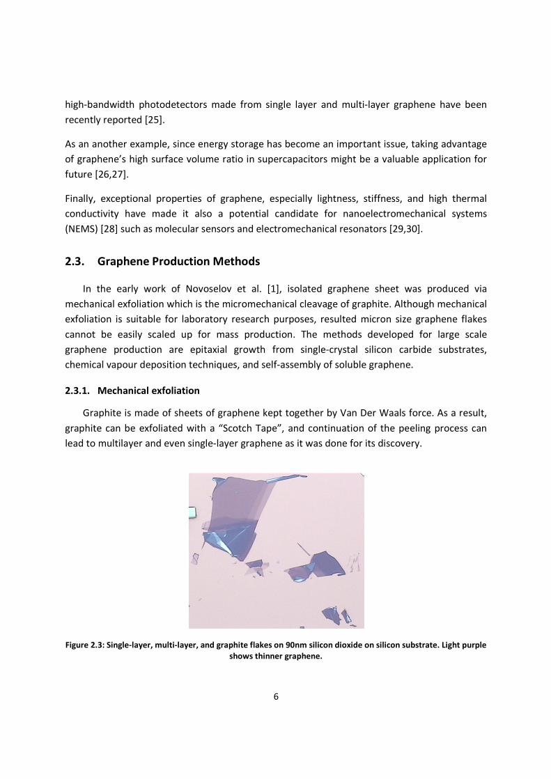
2.3.1. Mechanical exfoliation
Graphite is made of sheets of graphene kept together by Van Der Waals force. As a result,
graphite can be exfoliated with a “Scotch Tape”, and continuation of the peeling process can
lead to multilayer and even single-layer graphene as it was done for its discovery.
Figure 2.3: Single-layer, multi-layer, and graphite flakes on 90nm silicon dioxide on silicon substrate. Light purple
shows thinner graphene.
7
Next, the graphene flakes are transferred onto a suitable substrate such as silicon dioxide on
silicon with an oxide thickness of 90 nm or 300 nm in order to increase the contrast in visible
range and to identify graphene flakes [2]. At this point, one can locate and distinguish randomly
distributed single and multilayer-graphene flakes under microscope. In this condition, thick
graphene or graphite flakes appear more bluish, while few- layer and single layer-graphene will
look dark and light purple respectively, as it is illustrated in figure 2.3.
2.3.2. Epitaxial Growth on Silicon Carbide Single Crystal
This approach consists of sublimation of silicon atoms from the surface layers of silicon
carbide (0001) substrate at the temperature of about 1300˚C in an ultrahigh vacuum
environment [31,32]. Surface study shows the produced graphene layers, in this technique, are
strained with limited structural coherence length, 20 nm [26]. Although this method produces
graphene in larger scale than exfoliation method does, high temperature and high cost of
production are considered as serious hinder for application of this method.
2.3.3. Chemical Vapour Deposition
In this technique, a transition metal film such as Ni, Co, Pt, Ir or Ru is exposed to a
hydrocarbon gas. Under various temperatures and pressures dependant on the substrate metal
and gas type, carbon atoms dissolve into the metal surface and then force to precipitate by
cooling [33-35]. Several techniques have been developed to detach the produced graphene
sheet from the transition metal and transfer it to an appropriate insulating substrate [2]. CVD is
a promising technique for production of large area, high quality graphene especially for flat
displays and transparent electrode applications [36].
2.3.4. Self Assembly of Soluble graphene
In this method, graphene sheets can be prepared by Two-dimensional assembly of
graphene in solution phase [37]. Deposition of graphene from the solution can be also done
from reduction of graphene oxide [38]. Although graphene obtained by this method has still
relatively poor electrical quality, this technique shows the possibility of producing low cost and
large-scale graphene for flexible and transparent electronics [36].
2.4. Graphene field effect transistors
Electric field effect on graphene was one of the outstanding results showed by Novoselov
et al. [1]. As a consequence, extensive amount of research has been done on graphene field
effect transistors (GFETs) in which graphene is used as the channel material. In the beginning,
8
back-gate devices were being fabricated from exfoliated graphene on Si/SiO2 substrate in which
silicon and silicon dioxide served as back gate electrode and dielectric respectively. However,
since top-gate devices are much more desirable for applications, it did not take long for the
first top-gate graphene field effect device to emerge in 2007 [39].
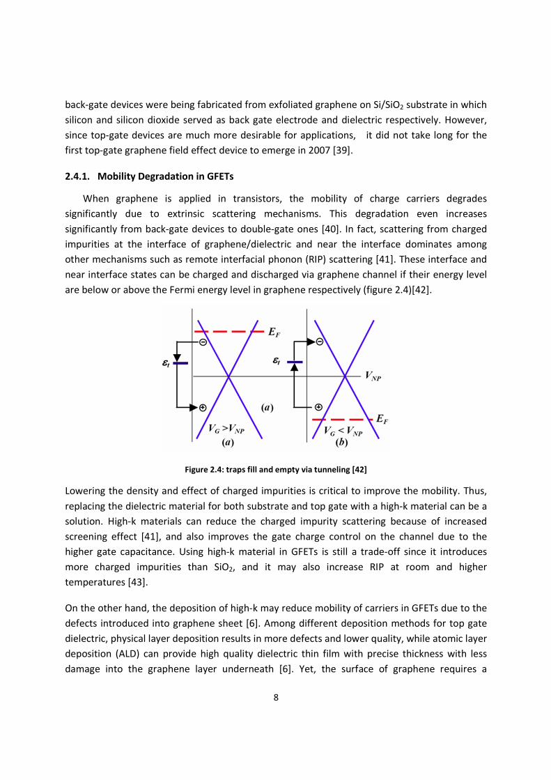
2.4.1. Mobility Degradation in GFETs
When graphene is applied in transistors, the mobility of charge carriers degrades
significantly due to extrinsic scattering mechanisms. This degradation even increases
significantly from back-gate devices to double-gate ones [40]. In fact, scattering from charged
impurities at the interface of graphene/dielectric and near the interface dominates among
other mechanisms such as remote interfacial phonon (RIP) scattering [41]. These interface and
near interface states can be charged and discharged via graphene channel if their energy level
are below or above the Fermi energy level in graphene respectively (figure 2.4)[42].
Figure 2.4: traps fill and empty via tunneling [42]
Lowering the density and effect of charged impurities is critical to improve the mobility. Thus,
replacing the dielectric material for both substrate and top gate with a high-k material can be a
solution. High-k materials can reduce the charged impurity scattering because of increased
screening effect [41], and also improves the gate charge control on the channel due to the
higher gate capacitance. Using high-k material in GFETs is still a trade-off since it introduces
more charged impurities than SiO2, and it may also increase RIP at room and higher
temperatures [43].
On the other hand, the deposition of high-k may reduce mobility of carriers in GFETs due to the
defects introduced into graphene sheet [6]. Among different deposition methods for top gate
dielectric, physical layer deposition results in more defects and lower quality, while atomic layer
deposition (ALD) can provide high quality dielectric thin film with precise thickness with less
damage into the graphene layer underneath [6]. Yet, the surface of graphene requires a
9
functionalization [44] or buffer layer [7] in order to be able using ALD for top gate dielectric
deposition. Significant research has been made not only to optimize ALD process, but also to
find other deposition techniques such as recently developed “Physical assembly of freestanding
dielectric nanostructures on graphene [6].”
2.4.2. Current-Voltage Characterics of GFETs
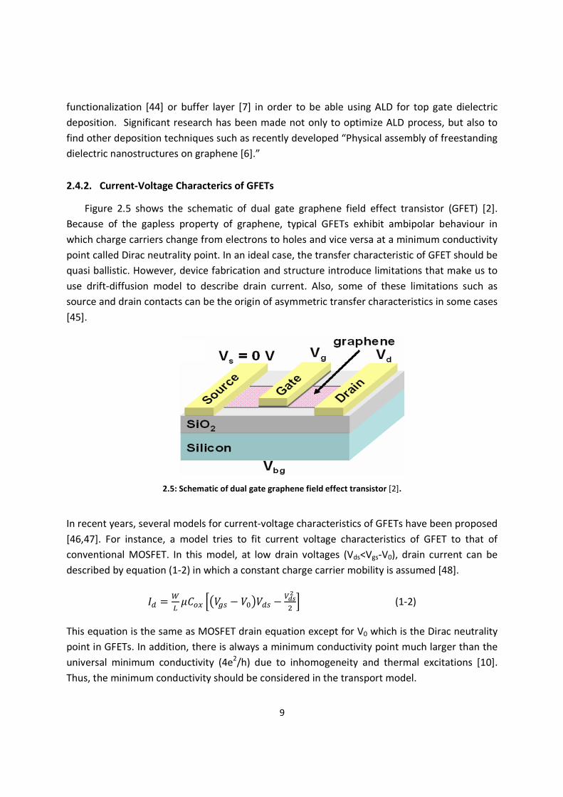
Figure 2.5 shows the schematic of dual gate graphene field effect transistor (GFET) [2].
Because of the gapless property of graphene, typical GFETs exhibit ambipolar behaviour in
which charge carriers change from electrons to holes and vice versa at a minimum conductivity
point called Dirac neutrality point. In an ideal case, the transfer characteristic of GFET should be
quasi ballistic. However, device fabrication and structure introduce limitations that make us to
use drift-diffusion model to describe drain current. Also, some of these limitations such as
source and drain contacts can be the origin of asymmetric transfer characteristics in some cases
[45].
2.5: Schematic of dual gate graphene field effect transistor [2].
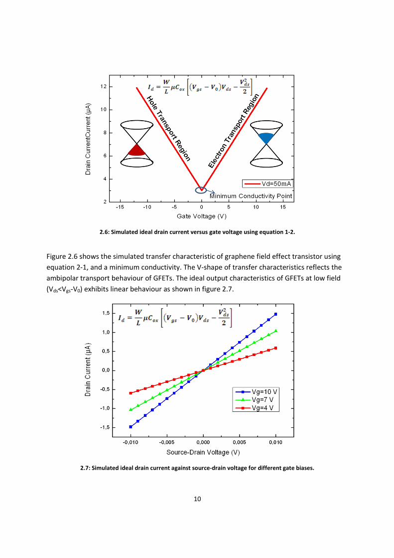
In recent years, several models for current-voltage characteristics of GFETs have been proposed
[46,47]. For instance, a model tries to fit current voltage characteristics of GFET to that of
conventional MOSFET. In this model, at low drain voltages (Vds<Vgs-V0), drain current can be
described by equation (1-2) in which a constant charge carrier mobility is assumed [48].
! "# !
$%&' ( (1-2)
This equation is the same as MOSFET drain equation except for V0 which is the Dirac neutrality
point in GFETs. In addition, there is always a minimum conductivity point much larger than the
universal minimum conductivity (4e2/h) due to inhomogeneity and thermal excitations [10].
Thus, the minimum conductivity should be considered in the transport model.
10
2.6: Simulated ideal drain current versus gate voltage using equation 1-2.
Figure 2.6 shows the simulated transfer characteristic of graphene field effect transistor using
equation 2-1, and a minimum conductivity. The V-shape of transfer characteristics reflects the
ambipolar transport behaviour of GFETs. The ideal output characteristics of GFETs at low field
(Vds<Vgs-V0) exhibits linear behaviour as shown in figure 2.7.
2.7: Simulated ideal drain current against source-drain voltage for different gate biases.
11
3. Fabrication
In this work, back-gate and top-gate graphene field effect transistors were fabricated
using exfoliated graphene on Si/SiO2 substrate. Silicon dioxide film was also served as back gate
dielectric, while Al2O3 was used as high-k top gate insulator deposited by atomic layer
deposition (ALD). In this chapter, fabrication process will be discussed.
3.1. Graphene Production
3.1.1. Substrate preparation
An appropriate substrate requires an insulator film with specific thickness for identification
of graphene on the substrate. Therefore, fabrication process started with thermal oxidation of
n-type silicon wafer in oxidation furnace. In order to have maximum contrast in visible light, 90
nm oxide thickness was chosen and 99 nm practical thickness was measured by ellipsometry.
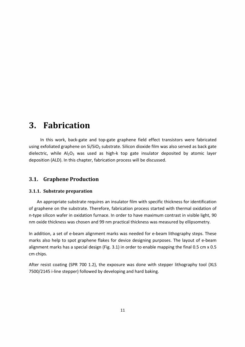
In addition, a set of e-beam alignment marks was needed for e-beam lithography steps. These
marks also help to spot graphene flakes for device designing purposes. The layout of e-beam
alignment marks has a special design (Fig. 3.1) in order to enable mapping the final 0.5 cm x 0.5
cm chips.
After resist coating (SPR 700 1.2), the exposure was done with stepper lithography tool (XLS
7500/2145 i-line stepper) followed by developing and hard baking.
12
Figure 3.1: The lay out for EBL alignment marks.
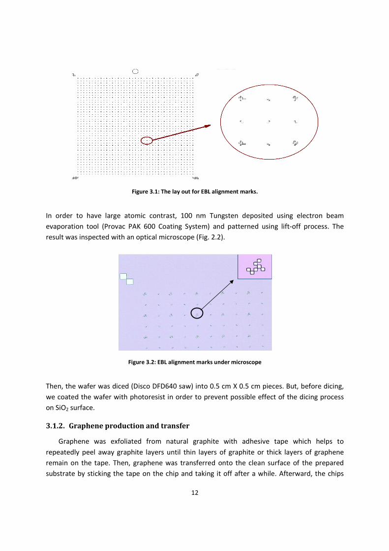
In order to have large atomic contrast, 100 nm Tungsten deposited using electron beam
evaporation tool (Provac PAK 600 Coating System) and patterned using lift-off process. The
result was inspected with an optical microscope (Fig. 2.2).
Figure 3.2: EBL alignment marks under microscope
Then, the wafer was diced (Disco DFD640 saw) into 0.5 cm X 0.5 cm pieces. But, before dicing,
we coated the wafer with photoresist in order to prevent possible effect of the dicing process
on SiO2 surface.
3.1.2. Graphene production and transfer
Graphene was exfoliated from natural graphite with adhesive tape which helps to
repeatedly peel away graphite layers until thin layers of graphite or thick layers of graphene
remain on the tape. Then, graphene was transferred onto the clean surface of the prepared
substrate by sticking the tape on the chip and taking it off after a while. Afterward, the chips

13
were inspected to find graphene flakes (fig. 3.3). Raman spectroscopy was applied to confirm
the single layer graphene, which will be discussed in the next chapter.
Figure 3.3: Graphene was exfoliated by adhesive tape and transferred onto the substrate (pictute on the right hand side). The most transparent flakes in the picture are single layer graphene while dark purple shows thicker
multilayer graphene.
3.2. Device Fabrication
Device fabrication initiated by device design followed by one or two steps of e-beam
lithography, metal deposition, high-k atomic layer deposition, and lift-off which we will briefly
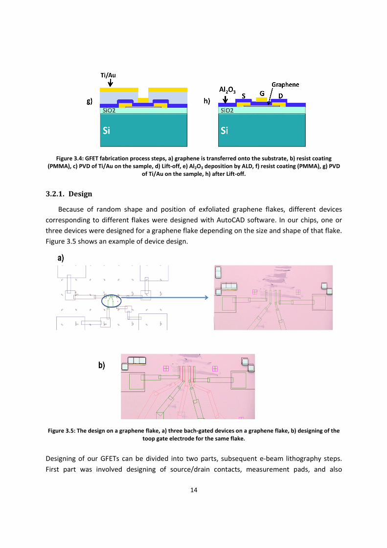
explain each in this part. The process steps are shown schematically in figure 3.4.
14
Figure 3.4: GFET fabrication process steps, a) graphene is transferred onto the substrate, b) resist coating (PMMA), c) PVD of Ti/Au on the sample, d) Lift-off, e) Al2O3 deposition by ALD, f) resist coating (PMMA), g) PVD
of Ti/Au on the sample, h) after Lift-off.
3.2.1. Design
Because of random shape and position of exfoliated graphene flakes, different devices
corresponding to different flakes were designed with AutoCAD software. In our chips, one or
three devices were designed for a graphene flake depending on the size and shape of that flake.
Figure 3.5 shows an example of device design.
Figure 3.5: The design on a graphene flake, a) three bach-gated devices on a graphene flake, b) designing of the
toop gate electrode for the same flake.
Designing of our GFETs can be divided into two parts, subsequent e-beam lithography steps.
First part was involved designing of source/drain contacts, measurement pads, and also
15
alignment marks for the second step of e-beam lithography (fig. 3.5.a). Second, the top gate
electrode and measurement pads were patterned (fig. 3.5.b).
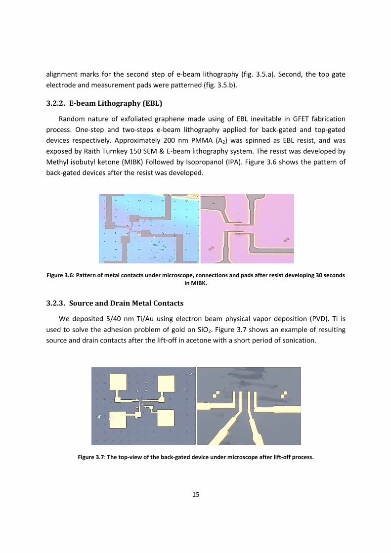
3.2.2. E-beam Lithography (EBL)
Random nature of exfoliated graphene made using of EBL inevitable in GFET fabrication
process. One-step and two-steps e-beam lithography applied for back-gated and top-gated
devices respectively. Approximately 200 nm PMMA (A2) was spinned as EBL resist, and was
exposed by Raith Turnkey 150 SEM & E-beam lithography system. The resist was developed by
Methyl isobutyl ketone (MIBK) Followed by Isopropanol (IPA). Figure 3.6 shows the pattern of
back-gated devices after the resist was developed.
Figure 3.6: Pattern of metal contacts under microscope, connections and pads after resist developing 30 seconds in MIBK.
3.2.3. Source and Drain Metal Contacts
We deposited 5/40 nm Ti/Au using electron beam physical vapor deposition (PVD). Ti is
used to solve the adhesion problem of gold on SiO2. Figure 3.7 shows an example of resulting
source and drain contacts after the lift-off in acetone with a short period of sonication.
Figure 3.7: The top-view of the back-gated device under microscope after lift-off process.
16
Now the back-gated GFET is ready for electrical characterization which will be discussed in next
chapter. At this step, we continue the process description to fabricate top-gate devices.
3.2.4. High k material deposition using ALD
As it was discussed in chapter one, applying a high k material as gate insulator can increase
both charge control and screening effect. However the deposition method is critical in order to
have fewer defects to the graphene sheet, and high quality high-k material. Atomic Layer
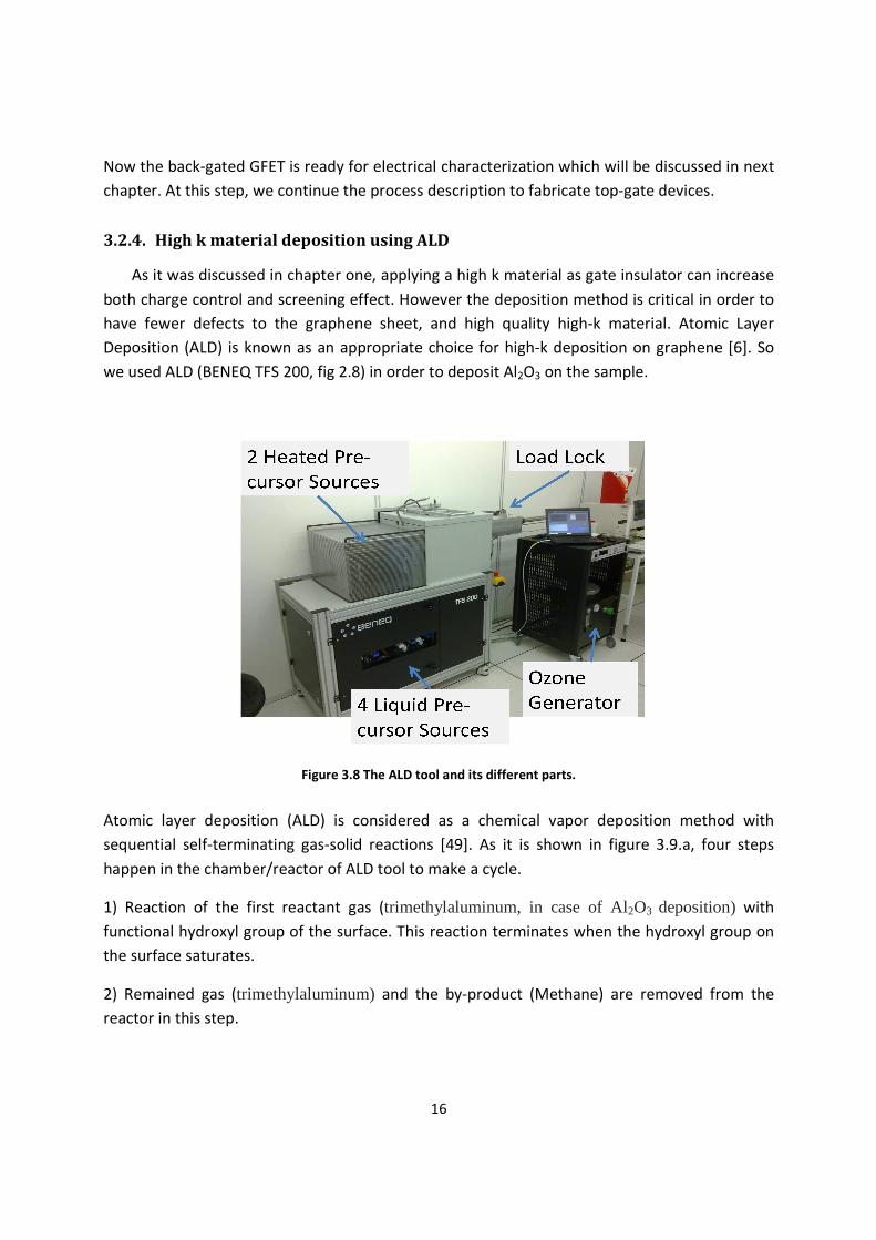
Deposition (ALD) is known as an appropriate choice for high-k deposition on graphene [6]. So
we used ALD (BENEQ TFS 200, fig 2.8) in order to deposit Al2O3 on the sample.
Figure 3.8 The ALD tool and its different parts.
Atomic layer deposition (ALD) is considered as a chemical vapor deposition method with
sequential self-terminating gas-solid reactions [49]. As it is shown in figure 3.9.a, four steps
happen in the chamber/reactor of ALD tool to make a cycle.
1) Reaction of the first reactant gas (trimethylaluminum, in case of Al2O3 deposition) with
functional hydroxyl group of the surface. This reaction terminates when the hydroxyl group on
the surface saturates.
2) Remained gas (trimethylaluminum) and the by-product (Methane) are removed from the
reactor in this step.

17
3) Pulsing the second reactant (water vapor) reactivates the surface. The reaction stops after
saturation of the surface.
4) The reactor is evacuated.
Repetition of this cycle provides desirable amount of deposited material on the surface. The
cross-flow reactor is shown schematically in figure 3.9.b.
Figure 3.9: a) shows four steps of a cycle in atomic layer deposition of Al2O3 It starts with flowing of
Trimethylaluminum into the reactor, reaction with functional group on the surface, puging of remained TMA and by-products, flowing of H2O into the reactor and reactivation of the surface, and finally purging the gases from reactor (www.beneq.com). b) Cross-flow reactor system wich is used in our ALD tool [50].
However, because of the absence of a functional group, direct ALD is not possible on the
surface of graphene. Using a thin film of oxidized metal could function as a nucleation layer for
ALD process [6].
So, 3-4 nm Aluminum was deposited on the sample using e-beam vapor deposition, and it was
exposed to the air for natural oxidation. Then, the sample was transferred to the ALD reactor
for annealing and in-situ Al2O3 deposition using trimethylaluminum and water vapor as reactant
18
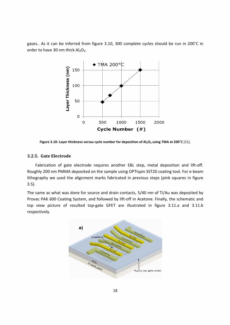
gases.. As it can be inferred from figure 3.10, 300 complete cycles should be run in 200˚C in
order to have 30 nm thick Al2O3.
Figure 3.10: Layer thickness versus cycle number for deposition of Al2O3 using TMA at 200˚C [51].
3.2.5. Gate Electrode
Fabrication of gate electrode requires another EBL step, metal deposition and lift-off.
Roughly 200 nm PMMA deposited on the sample using OPTIspin SST20 coating tool. For e-beam
lithography we used the alignment marks fabricated in previous steps (pink squares in figure
3.5).
The same as what was done for source and drain contacts, 5/40 nm of Ti/Au was deposited by
Provac PAK 600 Coating System, and followed by lift-off in Acetone. Finally, the schematic and
top view picture of resulted top-gate GFET are illustrated in figure 3.11.a and 3.11.b
respectively.
19
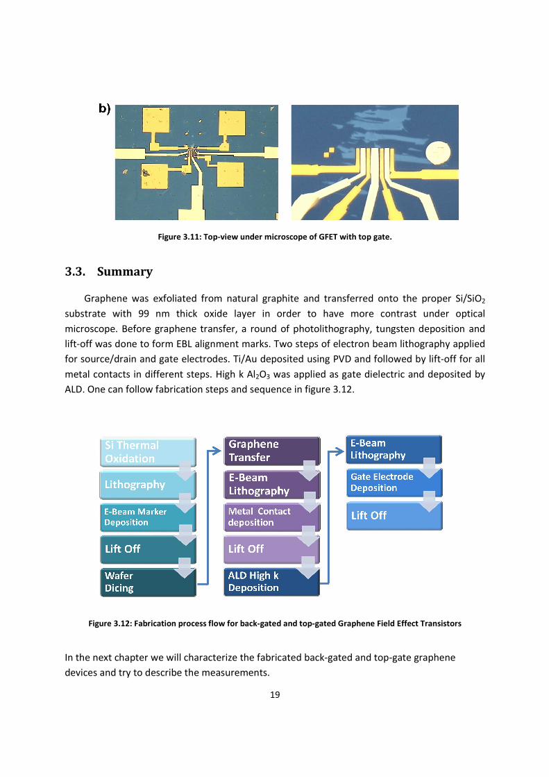
Figure 3.11: Top-view under microscope of GFET with top gate.
3.3. Summary
Graphene was exfoliated from natural graphite and transferred onto the proper Si/SiO2
substrate with 99 nm thick oxide layer in order to have more contrast under optical
microscope. Before graphene transfer, a round of photolithography, tungsten deposition and
lift-off was done to form EBL alignment marks. Two steps of electron beam lithography applied
for source/drain and gate electrodes. Ti/Au deposited using PVD and followed by lift-off for all
metal contacts in different steps. High k Al2O3 was applied as gate dielectric and deposited by
ALD. One can follow fabrication steps and sequence in figure 3.12.
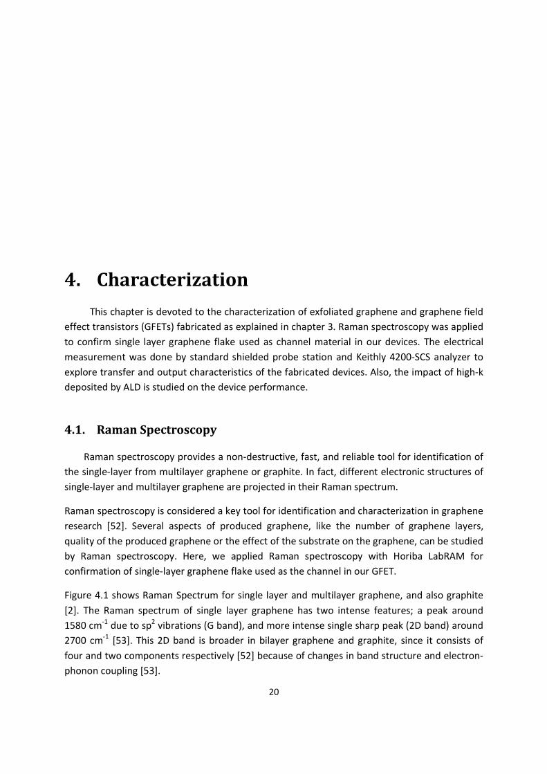
Figure 3.12: Fabrication process flow for back-gated and top-gated Graphene Field Effect Transistors
In the next chapter we will characterize the fabricated back-gated and top-gate graphene
devices and try to describe the measurements.
20
4. Characterization
This chapter is devoted to the characterization of exfoliated graphene and graphene field
effect transistors (GFETs) fabricated as explained in chapter 3. Raman spectroscopy was applied
to confirm single layer graphene flake used as channel material in our devices. The electrical
measurement was done by standard shielded probe station and Keithly 4200-SCS analyzer to
explore transfer and output characteristics of the fabricated devices. Also, the impact of high-k
deposited by ALD is studied on the device performance.
4.1. Raman Spectroscopy
Raman spectroscopy provides a non-destructive, fast, and reliable tool for identification of
the single-layer from multilayer graphene or graphite. In fact, different electronic structures of
single-layer and multilayer graphene are projected in their Raman spectrum.
Raman spectroscopy is considered a key tool for identification and characterization in graphene
research [52]. Several aspects of produced graphene, like the number of graphene layers,
quality of the produced graphene or the effect of the substrate on the graphene, can be studied
by Raman spectroscopy. Here, we applied Raman spectroscopy with Horiba LabRAM for
confirmation of single-layer graphene flake used as the channel in our GFET.
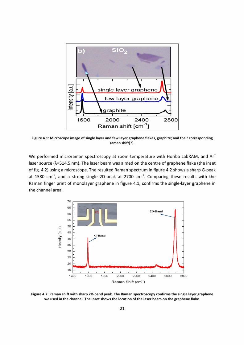
Figure 4.1 shows Raman Spectrum for single layer and multilayer graphene, and also graphite
[2]. The Raman spectrum of single layer graphene has two intense features; a peak around
1580 cm-1 due to sp2 vibrations (G band), and more intense single sharp peak (2D band) around
2700 cm-1 [53]. This 2D band is broader in bilayer graphene and graphite, since it consists of
four and two components respectively [52] because of changes in band structure and electron-
phonon coupling [53].
21
Figure 4.1: Microscope image of single layer and few layer graphene flakes, graphite; and their corresponding
raman shift[2].
We performed microraman spectroscopy at room temperature with Horiba LabRAM, and Ar+
laser source (λ=514.5 nm). The laser beam was aimed on the centre of graphene flake (the inset
of fig. 4.2) using a microscope. The resulted Raman spectrum in figure 4.2 shows a sharp G-peak
at 1580 cm-1, and a strong single 2D-peak at 2700 cm-1. Comparing these results with the
Raman finger print of monolayer graphene in figure 4.1, confirms the single-layer graphene in
the channel area.
Figure 4.2: Raman shift with sharp 2D-band peak. The Raman spectroscopy confirms the single layer graphene we used in the channel. The inset shows the location of the laser beam on the graphene flake.
22
In order to investigate the effect of Al2O3 deposition on the graphene flakes, Raman
spectroscopy was also performed for a sample after the deposition process. Its Raman
spectrum is shown in figure 4.3. The G-peak and strong single peak of 2D-band in this Raman
spectrum shows that still we have the single layer graphene. It means that the graphene’s
electronic structure is not mainly affected by the deposition process. In addition, having no
observable peak at 1350 cm-1 (D-band) which is a measure of defects in graphene crystal
implies that no damage is introduced to the graphene flake.
4.3: Raman spectrum for a graphene flake with Al2O3 deposited on top.
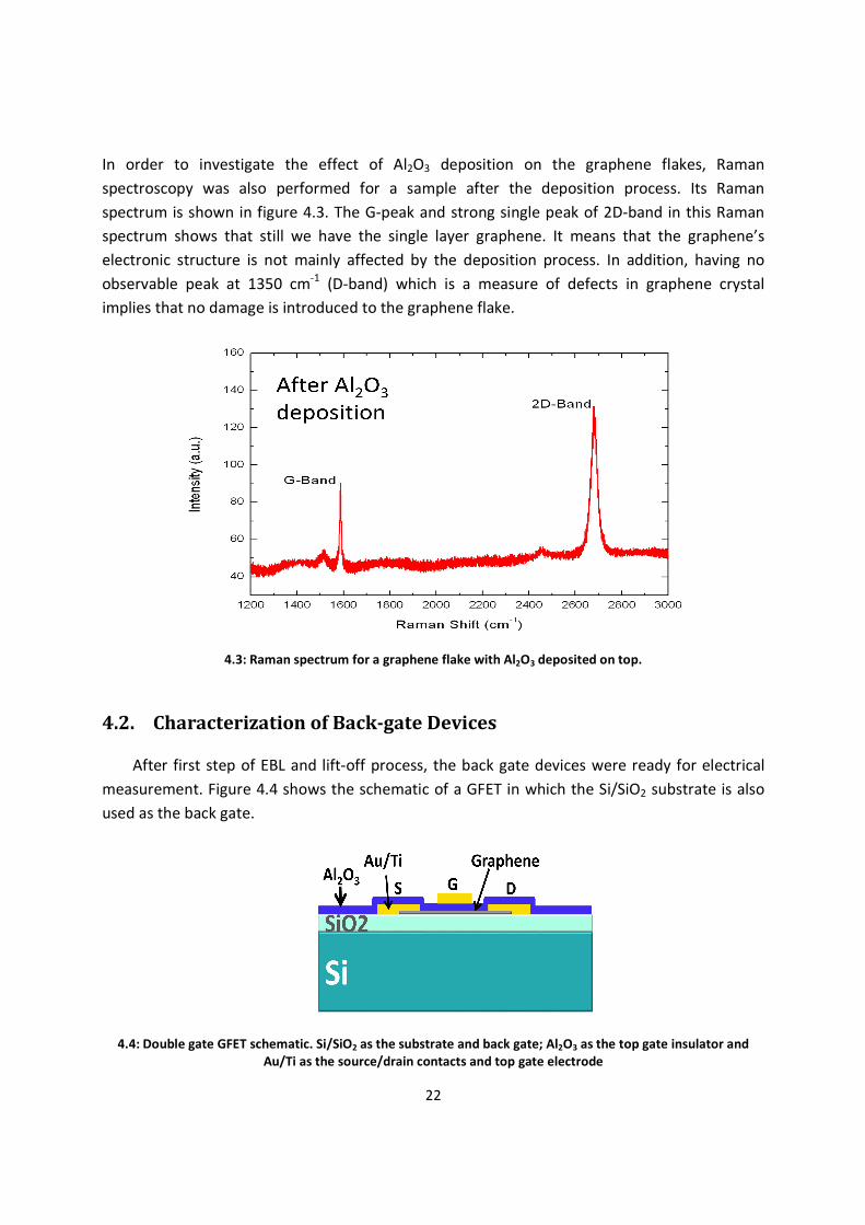
4.2. Characterization of Back-gate Devices
After first step of EBL and lift-off process, the back gate devices were ready for electrical
measurement. Figure 4.4 shows the schematic of a GFET in which the Si/SiO2 substrate is also
used as the back gate.
4.4: Double gate GFET schematic. Si/SiO2 as the substrate and back gate; Al2O3 as the top gate insulator and
Au/Ti as the source/drain contacts and top gate electrode
23
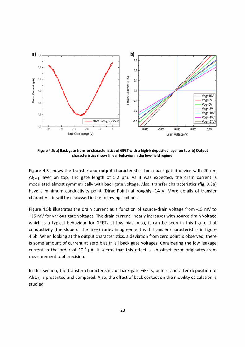
Figure 4.5: a) Back gate transfer characteristics of GFET with a high-k deposited layer on top. b) Output characteristics shows linear behavior in the low-field regime.
Figure 4.5 shows the transfer and output characteristics for a back-gated device with 20 nm
Al2O3 layer on top, and gate length of 5.2 µm. As it was expected, the drain current is
modulated almost symmetrically with back gate voltage. Also, transfer characteristics (fig. 3.3a)
have a minimum conductivity point (Dirac Point) at roughly -14 V. More details of transfer
characteristic will be discussed in the following sections.
Figure 4.5b illustrates the drain current as a function of source-drain voltage from -15 mV to
+15 mV for various gate voltages. The drain current linearly increases with source-drain voltage
which is a typical behaviour for GFETs at low bias. Also, it can be seen in this figure that
conductivity (the slope of the lines) varies in agreement with transfer characteristics in figure
4.5b. When looking at the output characteristics, a deviation from zero point is observed; there
is some amount of current at zero bias in all back gate voltages. Considering the low leakage
current in the order of 10-3 µA, it seems that this effect is an offset error originates from
measurement tool precision.
In this section, the transfer characteristics of back-gate GFETs, before and after deposition of
Al2O3, is presented and compared. Also, the effect of back contact on the mobility calculation is
studied.
24
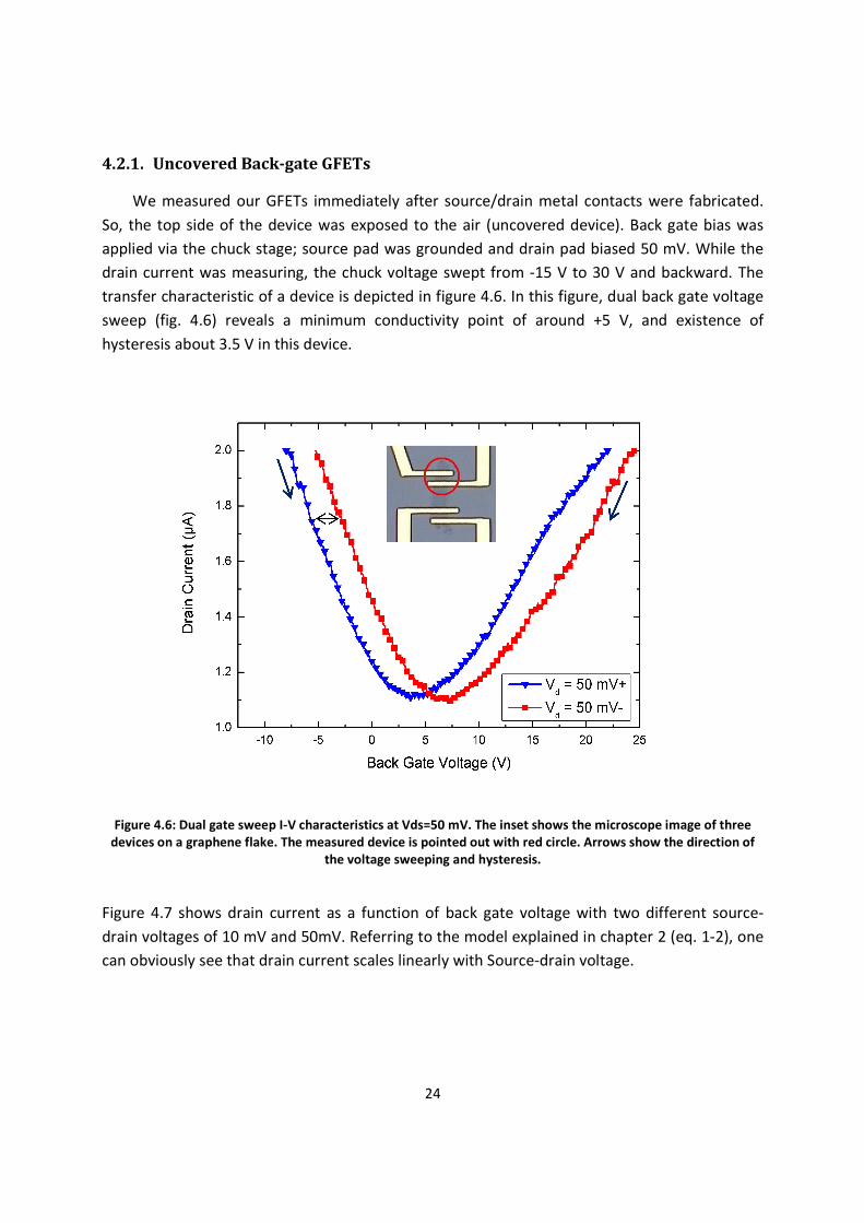
4.2.1. Uncovered Back-gate GFETs
We measured our GFETs immediately after source/drain metal contacts were fabricated.
So, the top side of the device was exposed to the air (uncovered device). Back gate bias was
applied via the chuck stage; source pad was grounded and drain pad biased 50 mV. While the
drain current was measuring, the chuck voltage swept from -15 V to 30 V and backward. The
transfer characteristic of a device is depicted in figure 4.6. In this figure, dual back gate voltage
sweep (fig. 4.6) reveals a minimum conductivity point of around +5 V, and existence of
hysteresis about 3.5 V in this device.
Figure 4.6: Dual gate sweep I-V characteristics at Vds=50 mV. The inset shows the microscope image of three devices on a graphene flake. The measured device is pointed out with red circle. Arrows show the direction of
the voltage sweeping and hysteresis.
Figure 4.7 shows drain current as a function of back gate voltage with two different source-
drain voltages of 10 mV and 50mV. Referring to the model explained in chapter 2 (eq. 1-2), one
can obviously see that drain current scales linearly with Source-drain voltage.
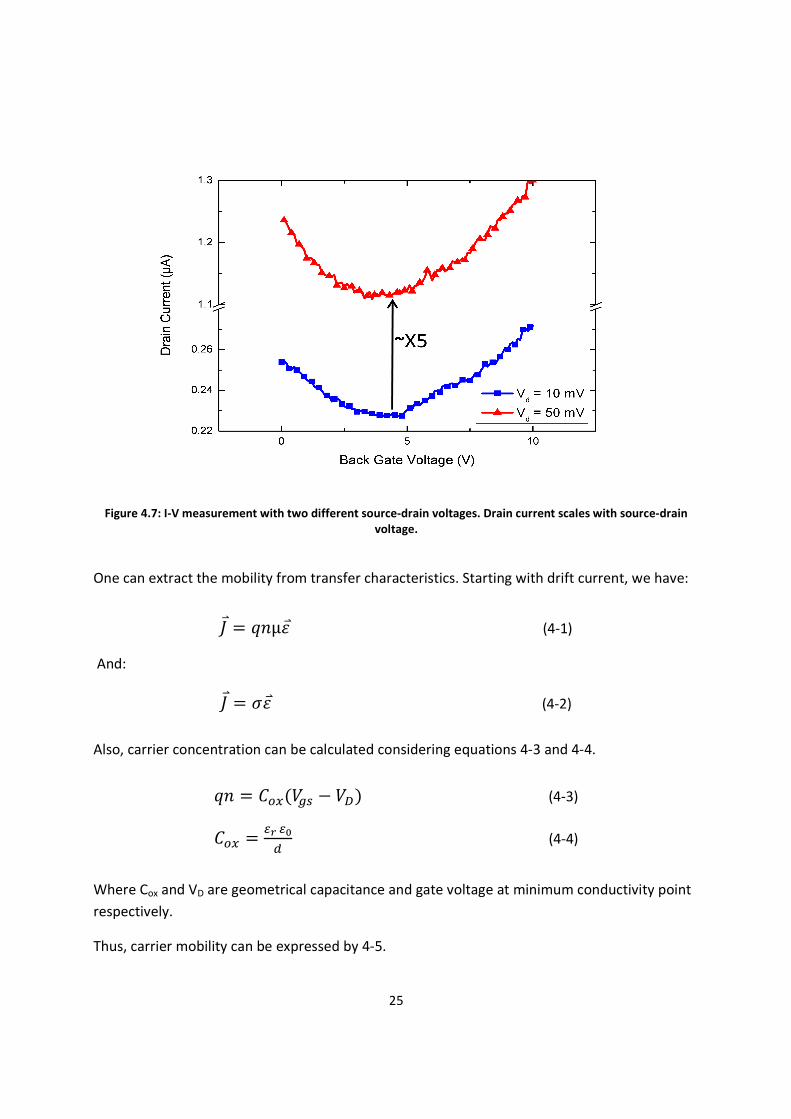
25
Figure 4.7: I-V measurement with two different source-drain voltages. Drain current scales with source-drain voltage.
One can extract the mobility from transfer characteristics. Starting with drift current, we have:
)* +,μ.* (4-1)
And:
)* /.* (4-2)
Also, carrier concentration can be calculated considering equations 4-3 and 4-4.
+, ! 0 (4-3)
1213 (4-4)
Where Cox and VD are geometrical capacitance and gate voltage at minimum conductivity point
respectively.
Thus, carrier mobility can be expressed by 4-5.
26
456
7%&8$%&889:;8$<&=$>
(4-5)
Applying this equation for devices with gate length of 1.2 µm and 5.2 µm at carrier
concentration of 1x1016 cm-2 results in mobilities of 55 cm2/V.s and 193 cm2/V.s respectively.
However, since there is always a nonzero minimum conductivity for graphene, using 7%&
$<&=$>
results in mobility over estimation [54]. Another method which is also used for mobility
extraction is based on transconductance which is the slope of linear part of Current-voltage
curve. Thus, we replace 7%&
$<&=$> with transconductance,? in 4-5. As a result, mobility is
expressed by 4-7.
7%&$<&=$>
→ ? (4-6)
A$%&∙9:;
∙ (4-7)
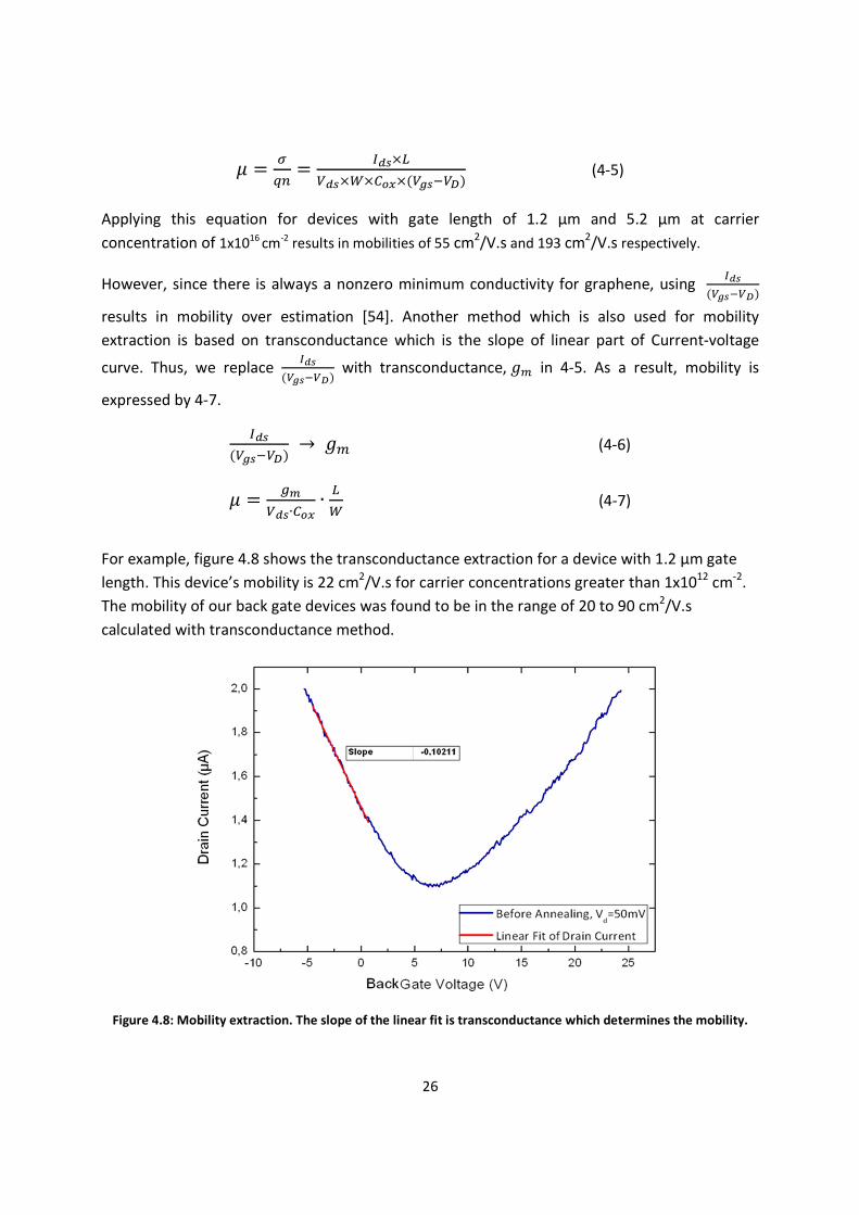
For example, figure 4.8 shows the transconductance extraction for a device with 1.2 µm gate
length. This device’s mobility is 22 cm2/V.s for carrier concentrations greater than 1x1012 cm-2.
The mobility of our back gate devices was found to be in the range of 20 to 90 cm2/V.s
calculated with transconductance method.
Figure 4.8: Mobility extraction. The slope of the linear fit is transconductance which determines the mobility.
27
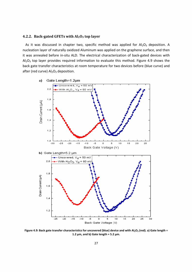
4.2.2. Back-gated GFETs with Al2O3 top layer
As it was discussed in chapter two, specific method was applied for Al2O3 deposition. A
nucleation layer of naturally oxidized Aluminum was applied on the graphene surface, and then
it was annealed before in-situ ALD. The electrical characterization of back-gated devices with
Al2O3 top layer provides required information to evaluate this method. Figure 4.9 shows the
back gate transfer characteristics at room temperature for two devices before (blue curve) and
after (red curve) Al2O3 deposition.
Figure 4.9: Back gate transfer characteristics for uncovered (blue) device and with Al2O3 (red). a) Gate length = 1.2 µm, and b) Gate length = 5.2 µm.
28
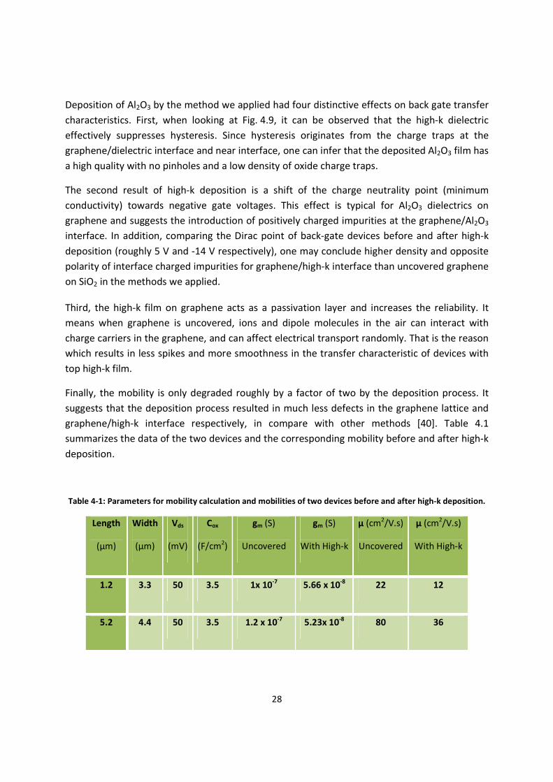
Deposition of Al2O3 by the method we applied had four distinctive effects on back gate transfer
characteristics. First, when looking at Fig. 4.9, it can be observed that the high-k dielectric
effectively suppresses hysteresis. Since hysteresis originates from the charge traps at the
graphene/dielectric interface and near interface, one can infer that the deposited Al2O3 film has
a high quality with no pinholes and a low density of oxide charge traps.
The second result of high-k deposition is a shift of the charge neutrality point (minimum
conductivity) towards negative gate voltages. This effect is typical for Al2O3 dielectrics on
graphene and suggests the introduction of positively charged impurities at the graphene/Al2O3
interface. In addition, comparing the Dirac point of back-gate devices before and after high-k
deposition (roughly 5 V and -14 V respectively), one may conclude higher density and opposite
polarity of interface charged impurities for graphene/high-k interface than uncovered graphene
on SiO2 in the methods we applied.
Third, the high-k film on graphene acts as a passivation layer and increases the reliability. It
means when graphene is uncovered, ions and dipole molecules in the air can interact with
charge carriers in the graphene, and can affect electrical transport randomly. That is the reason
which results in less spikes and more smoothness in the transfer characteristic of devices with
top high-k film.
Finally, the mobility is only degraded roughly by a factor of two by the deposition process. It
suggests that the deposition process resulted in much less defects in the graphene lattice and
graphene/high-k interface respectively, in compare with other methods [40]. Table 4.1
summarizes the data of the two devices and the corresponding mobility before and after high-k
deposition.
Table 4-1: Parameters for mobility calculation and mobilities of two devices before and after high-k deposition.
Length
(µm)
Width
(µm)
Vds
(mV)
Cox
(F/cm2)
gm (S)
Uncovered
gm (S)
With High-k
µ (cm2/V.s)
Uncovered
µ (cm2/V.s)
With High-k
1.2 3.3 50 3.5 1x 10⁻⁷ 5.66 x 10⁻⁸ 22 12
5.2 4.4 50 3.5 1.2 x 10⁻⁷ 5.23x 10⁻⁸ 80 36
29
4.3. Mobility Extraction: Limits and challenges
4.3.1. Series resistance
The extracted mobilities of our devices are quite small in comparison to reported values
which are in the order of several thousand for exfoliated graphene. Also, mobility varies with
gate length. Variation of mobility with gate length is in contrast with drift-diffusion model in
which scattering dominates the carrier transport in large gate length devices, and mobility
should be constant by changing the gate length. Since we applied transconductance method to
extract the mobility, let’s investigate the transconductance.
Considering equation 4-7, the transconductance should scale inversely with gate length:
A ∙ ∙ ∙ CD (4-7)
-30 -25 -20 -15 -10 -5 0 5 10
0,2
0,4
Dra
in C
urre
nt (
µA
/µm
)
Back Gate Voltage (V)
L=1.2µm L=1.2µm L=5.2µm
Vd = 60 mV
Vd = 30 mV
Figure 4.10: Drain current per width versus gate voltage, for three devices, applying source drain voltages of 30 mV (filled) and 60 mV (blank).
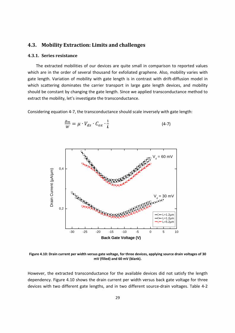
However, the extracted transconductance for the available devices did not satisfy the length
dependency. Figure 4.10 shows the drain current per width versus back gate voltage for three
devices with two different gate lengths, and in two different source-drain voltages. Table 4-2
30
shows the values of transconductance per width for these devices. The gm/w in these devices is
roughly constant by changing the gate length. This length independency explains variation of
extracted mobility with gate length.
On the other hand, if mobility should be considered as a constant, source-drain voltage
variation could be considered as the reason of gm/w length independency. In the following, we
investigate the series resistance and its probable effect on mobility extraction.
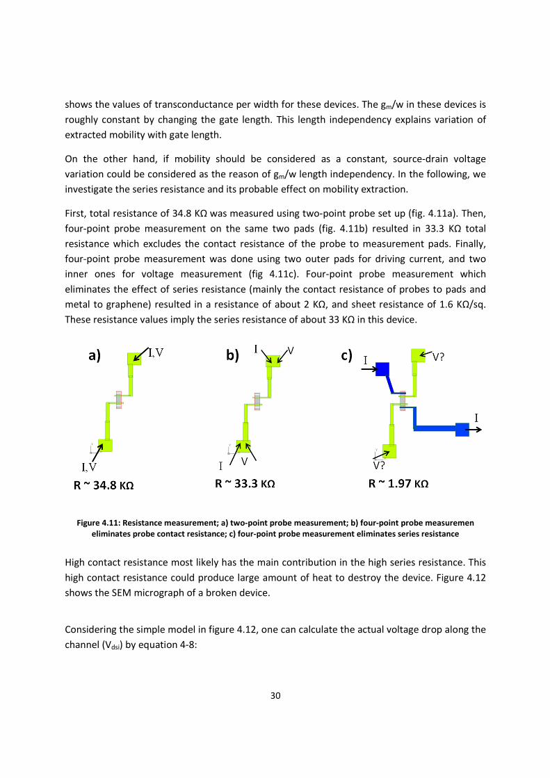
First, total resistance of 34.8 KΩ was measured using two-point probe set up (fig. 4.11a). Then,
four-point probe measurement on the same two pads (fig. 4.11b) resulted in 33.3 KΩ total
resistance which excludes the contact resistance of the probe to measurement pads. Finally,
four-point probe measurement was done using two outer pads for driving current, and two
inner ones for voltage measurement (fig 4.11c). Four-point probe measurement which
eliminates the effect of series resistance (mainly the contact resistance of probes to pads and
metal to graphene) resulted in a resistance of about 2 KΩ, and sheet resistance of 1.6 KΩ/sq.
These resistance values imply the series resistance of about 33 KΩ in this device.
Figure 4.11: Resistance measurement; a) two-point probe measurement; b) four-point probe measuremen eliminates probe contact resistance; c) four-point probe measurement eliminates series resistance
High contact resistance most likely has the main contribution in the high series resistance. This
high contact resistance could produce large amount of heat to destroy the device. Figure 4.12
shows the SEM micrograph of a broken device.
Considering the simple model in figure 4.12, one can calculate the actual voltage drop along the
channel (Vdsi) by equation 4-8:
31
E F GHIGHIJGK
L 8 (4-8)
Where RCh is the channel resistance, Rs is the total series resistance, and Vds is the source-drain
voltage.
Figure 4.12: A broken top-gate GFET. It involves a set of three devices.
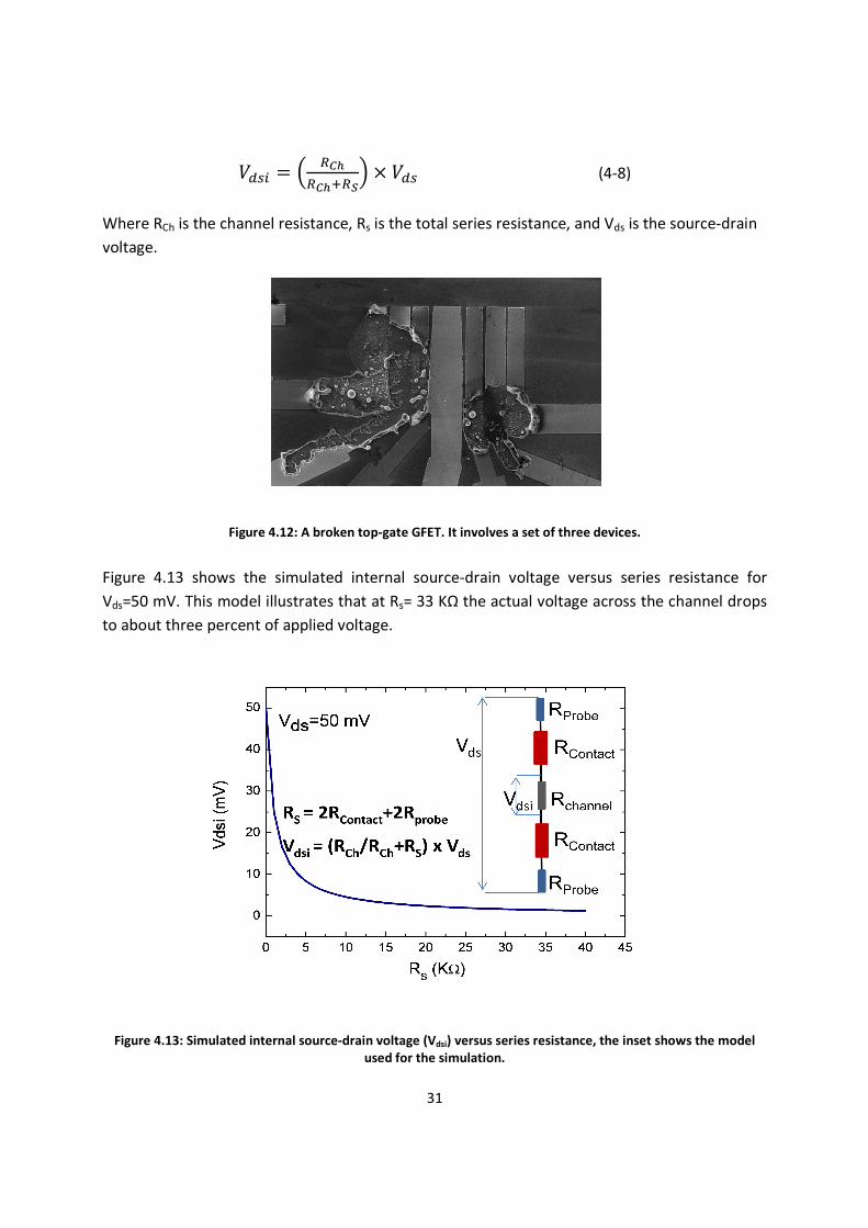
Figure 4.13 shows the simulated internal source-drain voltage versus series resistance for
Vds=50 mV. This model illustrates that at Rs= 33 KΩ the actual voltage across the channel drops
to about three percent of applied voltage.
Figure 4.13: Simulated internal source-drain voltage (Vdsi) versus series resistance, the inset shows the model used for the simulation.
32
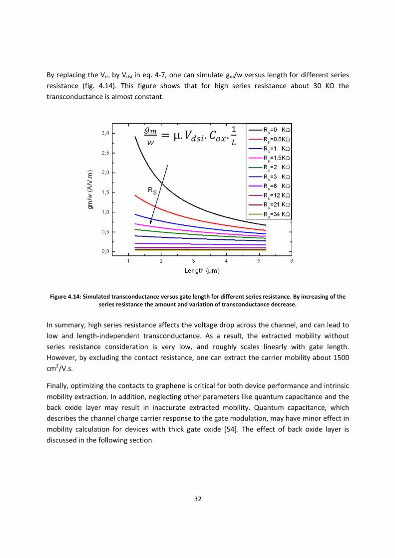
By replacing the Vds by Vdsi in eq. 4-7, one can simulate gm/w versus length for different series
resistance (fig. 4.14). This figure shows that for high series resistance about 30 KΩ the
transconductance is almost constant.
Figure 4.14: Simulated transconductance versus gate length for different series resistance. By increasing of the series resistance the amount and variation of transconductance decrease.
In summary, high series resistance affects the voltage drop across the channel, and can lead to
low and length-independent transconductance. As a result, the extracted mobility without
series resistance consideration is very low, and roughly scales linearly with gate length.
However, by excluding the contact resistance, one can extract the carrier mobility about 1500
cm2/V.s.
Finally, optimizing the contacts to graphene is critical for both device performance and intrinsic
mobility extraction. In addition, neglecting other parameters like quantum capacitance and the
back oxide layer may result in inaccurate extracted mobility. Quantum capacitance, which
describes the channel charge carrier response to the gate modulation, may have minor effect in
mobility calculation for devices with thick gate oxide [54]. The effect of back oxide layer is
discussed in the following section.
33
4.3.2. Back gate devices with Back contact
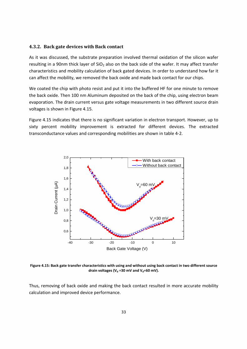
As it was discussed, the substrate preparation involved thermal oxidation of the silicon wafer
resulting in a 90nm thick layer of SiO2 also on the back side of the wafer. It may affect transfer
characteristics and mobility calculation of back gated devices. In order to understand how far it
can affect the mobility, we removed the back oxide and made back contact for our chips.
We coated the chip with photo resist and put it into the buffered HF for one minute to remove
the back oxide. Then 100 nm Aluminum deposited on the back of the chip, using electron beam
evaporation. The drain current versus gate voltage measurements in two different source drain
voltages is shown in Figure 4.15.
Figure 4.15 indicates that there is no significant variation in electron transport. However, up to
sixty percent mobility improvement is extracted for different devices. The extracted
transconductance values and corresponding mobilities are shown in table 4-2.
-40 -30 -20 -10 0 10
0,6
0,8
1,0
1,2
1,4
1,6
1,8
2,0
Vd=30 mV
Dra
in C
urre
nt (
µA
)
Back Gate Voltage (V)
With back contact Without back contact
Vd=60 mV
Figure 4.15: Back gate transfer characteristics with using and without using back contact in two different source drain voltages (Vd =30 mV and Vd=60 mV).
Thus, removing of back oxide and making the back contact resulted in more accurate mobility
calculation and improved device performance.
34
Table 4-2: Transconductance and mobility difference, before and after making back contacts for two different
source-drain voltages.
Vds
(mV)
Width
(µm)
Length
(µm)
Cox
(F/cm2)
gm (S)
Without Back
Contact
gm (S)
With Back
Contact
µ (cm2/V.s)
Without Back
Contact
µ (cm2/V.s)
With Back
Contact
30 3.3 1.2 3.5 2.46 x 10⁻⁸ 3.523 x 10⁻⁸ 8.6 12.3
60 3.3 1.2 3.5 5.12 x 10⁻⁸ 6.894x 10⁻⁸ 8.9 12
60 4.4 5.2 3.5 5.15 x 10⁻⁸ 8.8 x 10⁻⁸ 30 49
4.4. Characterization of top-gate devices
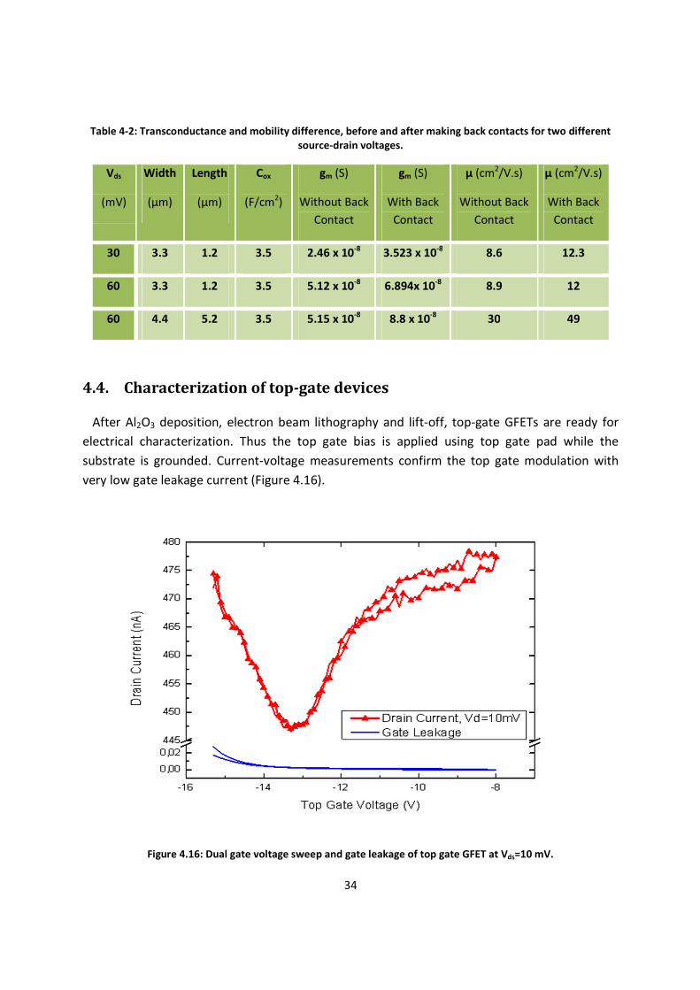
After Al2O3 deposition, electron beam lithography and lift-off, top-gate GFETs are ready for
electrical characterization. Thus the top gate bias is applied using top gate pad while the
substrate is grounded. Current-voltage measurements confirm the top gate modulation with
very low gate leakage current (Figure 4.16).
Figure 4.16: Dual gate voltage sweep and gate leakage of top gate GFET at Vds=10 mV.
35
In Fig. 4.16, dual gate voltage sweep measurement shows almost no hysteresis in this device
with gate length of 1.5 micron. Yet, the electron dominated transport at gate voltages greater
than 2 volts away from Dirac point has a non-ideal behaviour with some hysteresis. This
behaviour is not fully understood yet.
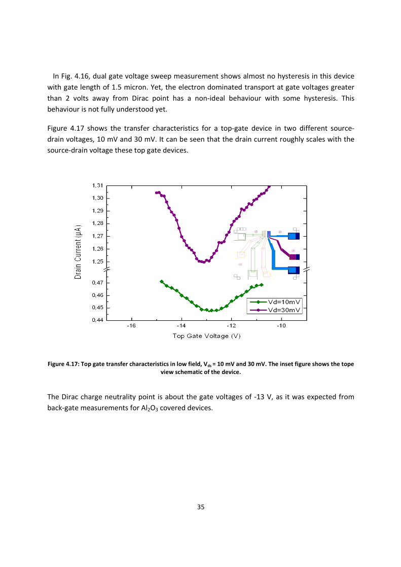
Figure 4.17 shows the transfer characteristics for a top-gate device in two different source-
drain voltages, 10 mV and 30 mV. It can be seen that the drain current roughly scales with the
source-drain voltage these top gate devices.
Figure 4.17: Top gate transfer characteristics in low field, Vds = 10 mV and 30 mV. The inset figure shows the tope view schematic of the device.
The Dirac charge neutrality point is about the gate voltages of -13 V, as it was expected from
back-gate measurements for Al2O3 covered devices.
36
5. Conclusion
In this project, first KTH’s back-gate and top-gate (dual-gate) GFETs have been successfully
designed, fabricated, and characterized. Electrical characterization confirmed the current
modulation in top-gated and back-gated devices in which single-layer exfoliated graphene was
used as the channel material. We also investigated hysteresis in double gated GFETs with a
20nm aluminum oxide (Al2O3) top gate dielectric which was deposited by atomic layer
deposition (ALD). We prepared a nucleation layer for the ALD growth by electron beam
evaporation of aluminum followed by natural oxidation. We then annealed the devices in
vacuum before in-situ ALD.
Back gate transfer characteristics, measured before and after Al2O3 deposition, shows that the
high-k dielectric effectively suppresses hysteresis, indicating a high quality film without pinholes
and a low density of oxide charge traps. A shift of the charge neutrality point towards negative
gate voltages was observed, which is typical for Al2O3 dielectrics on graphene. This suggests the
introduction of positively charged impurities at the graphene/Al2O3 interface. Finally, the
mobility is only degraded by a factor of about two through the deposition process.
The charge carrier mobility extraction resulted in rather low values in compare to the average
mobilities reported for GFETs using exfoliated graphene. It was enlightened that the main
reason of this low extracted mobility should be the existence of high series resistance. In
addition, oxidized layer on the back side of the chip, and neglecting the effect of quantum
capacitance in mobility may lead to inaccurate mobility calculation in some cases.
Although optimization of high-k deposition on graphene has resulted in less electrical quality
degradation in GFETs, the lack of a reliable method to extract the density of charged impurities
is observed. One methodology for future would be through capacitance voltage measurements

37
and modeling the gate capacitance with a capacitor network consisting of constant oxide
capacitance, quantum capacitance, and interface trap capacitance [42]. Another suggestion can
be the applying charge pumping method which already is used in conventional MOSFETs.
38
References
[1] K.S. Novoselov, a K. Geim, S.V. Morozov, D. Jiang, Y. Zhang, S.V. Dubonos, I.V. Grigorieva, and a a Firsov, “Electric field effect in atomically thin carbon films.,” Science (New York, N.Y.), vol. 306, Oct. 2004, pp. 666-9.
[2] M.C. Lemme, “Current Status of Graphene Transistors,” Solid State Phenomena, vol. 158, 2010, pp. 499-509.
[3] K. Bolotin, K. Sikes, Z. Jiang, M. Klima, G. Fudenberg, J. Hone, P. Kim, and H. Stormer, “Ultrahigh electron mobility in suspended graphene,” Solid State Communications, vol. 146, Jun. 2008, pp. 351-355.
[4] B.S.K. Banerjee, F. Ieee, L.F. Register, E. Tutuc, M. Ieee, D. Basu, S. Kim, D. Reddy, and A.H. Macdonald, “Graphene for CMOS and Beyond CMOS Applications,” Proceedings of the IEEE, vol. 98, 2010.
[5] T.J. Echtermeyer, M.C. Lemme, J. Bolten, M. Baus, M. Ramsteiner, and H. Kurz, “Graphene field-effect devices,” The European Physical Journal Special Topics, vol. 148, Sep. 2007, pp. 19-26.
[6] L. Liao and X. Duan, “Graphene–dielectric integration for graphene transistors,” Materials Science and Engineering: R: Reports, vol. 70, Nov. 2010, pp. 354-370.
[7] S. Kim, J. Nah, I. Jo, D. Shahrjerdi, L. Colombo, Z. Yao, E. Tutuc, and S.K. Banerjee, “Realization of a high mobility dual-gated graphene field-effect transistor with Al[sub 2]O[sub 3] dielectric,” Applied Physics Letters, vol. 94, 2009, p. 062107.
[8] P.R. Wallace, “The Band Theory of Graphite,” Physical Review, vol. 71, 1947, pp. 622-634.
[9] A. Castro Neto, F. Guinea, N. Peres, K. Novoselov, and A. Geim, “The electronic properties of graphene,” Reviews of Modern Physics, vol. 81, Jan. 2009, pp. 109-162.
[10] A.K. Geim and K.S. Novoselov, “The rise of graphene.,” Nature materials, vol. 6, Mar. 2007, pp. 183-91.
[11] K.S. Novoselov, a K. Geim, S.V. Morozov, D. Jiang, M.I. Katsnelson, I.V. Grigorieva, S.V. Dubonos, and a a Firsov, “Two-dimensional gas of massless Dirac fermions in graphene.,” Nature, vol. 438, Nov. 2005, pp. 197-200.
[12] M.S. Purewal, Y. Zhang, and P. Kim, “Unusual transport properties in carbon based nanoscaled materials: nanotubes and graphene,” Physica Status Solidi (B), vol. 243, Nov. 2006, pp. 3418-3422.
39
[13] C. Berger, Z. Song, X. Li, X. Wu, N. Brown, C. Naud, D. Mayou, T. Li, J. Hass, A.N. Marchenkov, E.H. Conrad, P.N. First, and W. a de Heer, “Electronic confinement and coherence in patterned epitaxial graphene.,” Science (New York, N.Y.), vol. 312, May. 2006, pp. 1191-6.
[14] S. Morozov, K. Novoselov, M. Katsnelson, F. Schedin, D. Elias, J. Jaszczak, and a Geim, “Giant Intrinsic Carrier Mobilities in Graphene and Its Bilayer,” Physical Review Letters, vol. 100, Jan. 2008, pp. 11-14.
[15] E. Hwang, S. Adam, and S. Sarma, “Carrier Transport in Two-Dimensional Graphene Layers,” Physical Review Letters, vol. 98, May. 2007, pp. 2-5.
[16] A. a Balandin, S. Ghosh, W. Bao, I. Calizo, D. Teweldebrhan, F. Miao, and C.N. Lau, “Superior thermal conductivity of single-layer graphene.,” Nano letters, vol. 8, Mar. 2008, pp. 902-7.
[17] P. Blake, P.D. Brimicombe, R.R. Nair, T.J. Booth, D. Jiang, F. Schedin, L. a Ponomarenko, S.V. Morozov, H.F. Gleeson, E.W. Hill, A.K. Geim, and K.S. Novoselov, “Graphene-based liquid crystal device.,” Nano letters, vol. 8, Jun. 2008, pp. 1704-8.
[18] T.J. Booth, P. Blake, R.R. Nair, D. Jiang, E.W. Hill, U. Bangert, A. Bleloch, M. Gass, K.S. Novoselov, M.I. Katsnelson, and a K. Geim, “Macroscopic graphene membranes and their extraordinary stiffness.,” Nano letters, vol. 8, Aug. 2008, pp. 2442-6.
[19] M. Han, B. Özyilmaz, Y. Zhang, and P. Kim, “Energy Band-Gap Engineering of Graphene Nanoribbons,” Physical Review Letters, vol. 98, May. 2007, pp. 1-4.
[20] X. Li, X. Wang, L. Zhang, S. Lee, and H. Dai, “Chemically derived, ultrasmooth graphene nanoribbon semiconductors.,” Science (New York, N.Y.), vol. 319, Feb. 2008, pp. 1229-32.
[21] Y.-M. Lin, C. Dimitrakopoulos, K. a Jenkins, D.B. Farmer, H.-Y. Chiu, a Grill, and P. Avouris, “100-GHz transistors from wafer-scale epitaxial graphene.,” Science (New York, N.Y.), vol. 327, Feb. 2010, p. 662.
[22] J. Moser, A. Barreiro, and A. Bachtold, “Current-induced cleaning of graphene,” International Materials Reviews, pp. 3-6.
[23] F. Schwierz, “Graphene transistors,” Nature Nanotechnology, vol. 5, May. 2010, pp. 487-496.
[24] P. Avouris, “Graphene: Electronic and Photonic Properties and Devices,” Nano Letters, Sep. 2010, p. 100929092847080.
[25] F. Xia, T. Mueller, Y.-M. Lin, A. Valdes-Garcia, and P. Avouris, “Ultrafast graphene photodetector.,” Nature nanotechnology, vol. 4, Dec. 2009, pp. 839-43.
40
[26] Y. Wang, Z. Shi, Y. Huang, Y. Ma, C. Wang, M. Chen, and Y. Chen, “Supercapacitor Devices Based on Graphene Materials,” The Journal of Physical Chemistry C, vol. 113, Jul. 2009, pp. 13103-13107.
[27] M.D. Stoller, S. Park, Y. Zhu, J. An, and R.S. Ruoff, “Graphene-based ultracapacitors.,” Nano letters, vol. 8, Oct. 2008, pp. 3498-502.
[28] A.K. Geim, “Graphene: status and prospects.,” Science (New York, N.Y.), vol. 324, Jun. 2009, pp. 1530-4.
[29] J.T. Robinson, F.K. Perkins, E.S. Snow, Z. Wei, and P.E. Sheehan, “Reduced graphene oxide molecular sensors.,” Nano letters, vol. 8, Oct. 2008, pp. 3137-40.
[30] J.S. Bunch, A.M. van der Zande, S.S. Verbridge, I.W. Frank, D.M. Tanenbaum, J.M. Parpia, H.G. Craighead, and P.L. McEuen, “Electromechanical resonators from graphene sheets.,” Science (New York, N.Y.), vol. 315, Jan. 2007, pp. 490-3.
[31] C. Berger, Z. Song, T. Li, X. Li, A.Y. Ogbazghi, R. Feng, Z. Dai, A.N. Marchenkov, E.H. Conrad, P.N. First, and W. a de Heer, “Ultrathin Epitaxial Graphite: 2D Electron Gas Properties and a Route toward Graphene-based Nanoelectronics,” The Journal of Physical Chemistry B, vol. 108, Dec. 2004, pp. 19912-19916.
[32] W. Deheer, C. Berger, X. Wu, P. First, E. Conrad, X. Li, T. Li, M. Sprinkle, J. Hass, and M. Sadowski, “Epitaxial graphene,” Solid State Communications, vol. 143, Jul. 2007, pp. 92-100.
[33] A. Obraztsov, E. Obraztsova, A. Tyurnina, and A. Zolotukhin, “Chemical vapor deposition of thin graphite films of nanometer thickness,” Carbon, vol. 45, Sep. 2007, pp. 2017-2021.
[34] A. Reina, X. Jia, J. Ho, D. Nezich, H. Son, V. Bulovic, M.S. Dresselhaus, and J. Kong, “Large area, few-layer graphene films on arbitrary substrates by chemical vapor deposition.,” Nano letters, vol. 9, Jan. 2009, pp. 30-5.
[35] J. Coraux, A.T. NDiaye, C. Busse, and T. Michely, “Structural coherency of graphene on Ir(111).,” Nano letters, vol. 8, Feb. 2008, pp. 565-70.
[36] K.S. Kim, Y. Zhao, H. Jang, S.Y. Lee, J.M. Kim, K.S. Kim, J.-H. Ahn, P. Kim, J.-Y. Choi, and B.H. Hong, “Large-scale pattern growth of graphene films for stretchable transparent electrodes.,” Nature, vol. 457, Feb. 2009, pp. 706-10.
[37] X. Li, G. Zhang, X. Bai, X. Sun, X. Wang, E. Wang, and H. Dai, “Highly conducting graphene sheets and Langmuir-Blodgett films.,” Nature nanotechnology, vol. 3, Sep. 2008, pp. 538-42.
41
[38] G. Eda, G. Fanchini, and M. Chhowalla, “Large-area ultrathin films of reduced graphene oxide as a transparent and flexible electronic material.,” Nature nanotechnology, vol. 3, May. 2008, pp. 270-4.
[39] M.C. Lemme, T.J. Echtermeyer, M. Baus, and H. Kurz, “A Graphene Field-Effect Device,” IEEE Electron Device Letters, vol. 28, Apr. 2007, pp. 282-284.
[40] M. Lemme, T. Echtermeyer, M. Baus, B. Szafranek, J. Bolten, M. Schmidt, T. Wahlbrink, and H. Kurz, “Mobility in graphene double gate field effect transistors,” Solid-State Electronics, vol. 52, Feb. 2008, pp. 514-518.
[41] J.-H. Chen, C. Jang, S. Adam, M.S. Fuhrer, E.D. Williams, and M. Ishigami, “Charged-impurity scattering in graphene,” Nature Physics, vol. 4, Apr. 2008, pp. 377-381.
[42] Zebrev, “Quantum Capacitance vs Chemical Potential Universal Curve and Interface Trap Parameter Extraction in Graphene Gated StructuresNo Title,” Interface, pp. 1-13.
[43] J.-H. Chen, C. Jang, M. Ishigami, S. Xiao, W.G. Cullen, E.D. Williams, and M.S. Fuhrer, “Diffusive charge transport in graphene on SiO2,” Solid State Communications, vol. 149, Jul. 2009, pp. 1080-1086.
[44] X. Wang, S.M. Tabakman, and H. Dai, “Atomic layer deposition of metal oxides on pristine and functionalized graphene.,” Journal of the American Chemical Society, vol. 130, Jul. 2008, pp. 8152-3.
[45] S. Xu and Q. Zhang, “Causes of asymmetry in graphene transfer characteristics,” 2010 International Workshop on Junction Technology Extended Abstracts, May. 2010, pp. 1-3.
[46] S. a Thiele, J. a Schaefer, and F. Schwierz, “Modeling of graphene metal-oxide-semiconductor field-effect transistors with gapless large-area graphene channels,” Journal of Applied Physics, vol. 107, 2010, p. 094505.
[47] H. Wang, S. Member, A. Hsu, J. Kong, D.A. Antoniadis, and T. Palacios, “Compact Virtual-Source Current – Voltage Model for Top- and Back-Gated Graphene Field-Effect Transistors,” vol. 58, 2011, pp. 1523-1533.
[48] P. Palestri, private communication, 2010.
[49] R.L. Puurunen, “Surface chemistry of atomic layer deposition: A case study for the trimethylaluminum/water process,” Journal of Applied Physics, vol. 97, 2005, p. 121301.
[50] E. Granneman, P. Fischer, D. Pierreux, H. Terhorst, and P. Zagwijn, “Batch ALD: Characteristics, comparison with single wafer ALD, and examples,” Surface and Coatings Technology, vol. 201, Sep. 2007, pp. 8899-8907.
[51] M. Manouchehri and C. Henkel, “private communication,” 2010.

42
[52] A. Ferrari, “Raman spectroscopy of graphene and graphite: Disorder, electron–phonon coupling, doping and nonadiabatic effects,” Solid State Communications, vol. 143, Jul. 2007, pp. 47-57.
[53] A. Ferrari, J. Meyer, V. Scardaci, C. Casiraghi, M. Lazzeri, F. Mauri, S. Piscanec, D. Jiang, K. Novoselov, S. Roth, and A. Geim, “Raman Spectrum of Graphene and Graphene Layers,” Physical Review Letters, vol. 97, Oct. 2006, pp. 1-4.
[54] Z. Chen and J. Appenzeller, “Mobility extraction and quantum capacitance impact in high performance graphene field-effect transistor devices,” 2008 IEEE International Electron Devices Meeting, Dec. 2008, pp. 1-4.