fabrication, characterizationand hall mobility …
TRANSCRIPT

FABRICATION, CHARACTERIZATION AND HALL MOBILITY ANALYSIS OF
MOS DEVICES WITH LOW K AND HIGH K DIELECTRIC MATERIALS
by
RAKSHIT AGRAWAL
Presented to the Faculty of the Graduate School of
The University of Texas at Arlington in Partial Fulfillment
of the Requirements
for the Degree of
MASTER OF SCIENCE IN ELECTRICAL ENGINEERING
THE UNIVERSITY OF TEXAS AT ARLINGTON
December 2006

Copyright © by Rakshit Agrawal 2006
All Rights Reserved

iii
ACKNOWLEDGEMENTS
I would like to thank Dr. Wiley P. Kirk for giving me a great opportunity to
work on this project. His invaluable guidance and motivation has been primarily
instrumental in my Master’s research over the last one and a half years. He gave me
ample freedom to express my views and implement my ideas and encouraged me
throughout, which gave me a good insight of some of the most difficult and interesting
aspects of semiconductor processing and characterization.
I would like to thank Dr. Zeynep Celik-Butler and Dr. Weidong Zhou for being
part of my thesis committee.
I would also like to thank Mr. Robert T. Bate whose insight and guidance have
been very important and encouraging towards the completion of my thesis.
I have had an opportunity to work with some very talented colleagues, both past
and present. I would like to thank Dr. Kevin Clark and Mr. Eduardo Maldonado who
have been a terrific support both inside the UTA NanoFab Center cleanroom where a
large part of my project was carried out as well as in the ARS measurements laboratory.
Many thanks to other members of my research group Karan Deep, Moshe Davis,
Sharukh Chinoy, Rahul Mahajan and Y. Sampathkumar for their support and help. I
would also like to thank Vinayak Shamanna and Ram Subramanium for sharing their
views and ideas with me. I would like to thank Dr. Nasir Basit and Mr. Dennis Beuno

iv
for their help with the equipment training. I am thankful to all my other colleagues at
the NanoFab Center for their help and support at various stages of this project.
Last but not the least, I would like to thank my family Chandita, my sisters
Ruchika and Saakshi, and my parents Navin and Vibha for their tremendous support
and encouragement over the course of my studies here. I dedicate this thesis to them.
November 22, 2006

v
ABSTRACT
FABRICATION, CHARACTERIZATION AND HALL MOBILITY ANALYSIS ON
MOS DEVICES WITH LOW K AND HIGH K DIELECTRIC MATERIALS
Publication No. ______
Rakshit Agrawal, M.S.
The University of Texas at Arlington, 2006
Supervising Professor: Dr. Wiley P. Kirk
Scaling of MOSFETS has led to leakage current problems in SiO2 dielectric
based MOSFETS. This has led to the introduction of high-k dielectric materials which
can afford greater physical thickness and achieve the same capacitance with lesser
equivalent oxide thickness. But the high-k devices have certain limitations like channel
mobility degradation. Mobility degradation in high-k MISFETS is discussed in this
work using Hall measurements.
The MOS devices were fabricated with SiO2 and HfSiO, on p-type silicon
substrate. The fabrication process flow used for both type of MOS devices is explained.
Characterization and analysis was performed for the determination of various
parameters related to these devices like dielectric thickness. Hall mobility

vi
measurements were performed on the specially designed multi-drain Hall bars for
different gate biases in low magnetic field regime. Higher Hall mobility was observed
in the SiO2 based devices than HfSiO based devices.

vii
TABLE OF CONTENTS
ACKNOWLEDGEMENTS...................................................................................... iii
ABSTRACT.............................................................................................................. v
LIST OF ILLUSTRATIONS.................................................................................... x
LIST OF TABLES.................................................................................................... xviii
Chapter Page
1. INTRODUCTION ………………................................................................. 1
1.1 Historical Perspective ............................................................................. 1
1.2 Theory of MOSFETS.............................................................................. 5
1.2.1 Structure of MOSFET…………………………………………... 6
1.2.2 The MOS system under External Bias-Operating Modes
of a MOSFET…………………………………………………… 8
1.2.3 Threshold Voltage………………………………………………. 12
1.2.4 Gate Oxide………………………………………………………. 14
1.2.5 Carrier Mobility and Current Density…………………………… 15
1.3 Channel Mobility Degradation Mechanisms in a MOSFET……………… 18
1.3.1 Charge Scattering Mechanisms…………………………………. 19
1.3.2 Charge Trapping Mechanisms…………………………………… 23
1.4 High-K Dielectric Materials as an Alternative to SiO2……………........ 27
1.5 Mobility Degradation in High-K Dielectric Materials…………………. 34

viii
1.6 Methods of Mobility Extraction………………………………………... 37
1.6.1 The Hall Effect………………………………………………... 37
1.6.2 Split C-V Measurements……………………………………… 41
2. FABRICATION OF MOS DEVICES……………………………………… 44
2.1 Introduction……………………………………………………………... 44
2.2 Fabrication of MOS Devices................................................................... 50
2.3 Fabricated Devices and Dimensions……………………………………. 60
3. CHARACTERIZATION OF MOS DEVICES…………………………….. 75
3.1 Introduction……………………………………………………………... 75
3.1.1 Current-Voltage (I-V) Characteristics………………………… 75
3.1.2 Capacitance-Voltage (C-V) Characteristics…………………… 78
3.2 Measurement Method and Equipment………………………………….. 82
3.3 Experimental I-V characteristics……………………………………….. 84
3.3.1 Samples with SiO2 as Gate Dielectric………………………….. 84
3.3.2 Samples with HfSiO as Gate Dielectric………………………… 91
3.4 Experimental C-V characteristics………………………………………. 99
3.4.1 Samples with SiO2 as Gate Dielectric………………………….. 99
3.4.2 Samples with HfSiO as Gate Dielectric………………………… 112
4. HALL MOBILITY MEASUREMENTS....................................................... 126
4.1 Introduction……………………………………………………………... 126
4.2 Packaging……………………………………………………………….. 129
4.3 Hall Mobility Measurement Method and Measurement Equipment…… 134

ix
4.4 Hall Mobility Measurements-Experimental Results…………………… 138
4.4.1 Samples with SiO2 as Gate Dielectric...................................... 139
4.4.2 Samples with HfSiO as Gate Dielectric................................... 161
4.5 Comparison of Hall Mobility in SiO2 and HfSiO samples ..................... 168
5. CONCLUSION……………………………………………………………... 172
5.1 Summary………………………………………………………………… 172
5.2 Future Work……………………………………………………………... 175
APPENDIX
A. MASKS FOR FABRICATION ................................................................. 178
B. FABRICATION RECIPES ....................................................................... 182
REFERENCES.......................................................................................................... 195
BIOGRAPHICAL INFORMATION........................................................................ 204

x
LIST OF ILLUSTRATIONS
Figure Page
1.1 Moore’s law of scaling .................................................................................... 2
1.2 Different kinds of MOSFETS ......................................................................... 6
1.3 Basic structure of an n-channel MOSFET....................................................... 7
1.4 Energy band diagram of a MOS system operating in
accumulation………………………………………………………………..... 9
1.5 a) Energy band diagram of a MOS system operating in depletion
b) Cross-sectional view of a MOS system operating in depletion................... 10
1.6 a) Energy band diagram of a MOS system operating in inversion
b) Cross-sectional view of a MOS system operating in inversion................... 11
1.7 Random motion of carriers in a semiconductor with and without
applied electric field ...................................................................................... 16
1.8 Electron and hole mobility versus doping density for silicon ......................... 21
1.9 Temperature dependence of the surface roughness limited mobility ............. 23
1.10 Fixed charge effects on the capacitance-voltage curve of a MOS system ...... 24
1.11 Four categories of oxide charges in a MOS system......................................... 24
1.12 High-k for gate dielectrics ............................................................................... 29
1.13 Conduction band and valence band offsets of various oxides
on Silicon ......................................................................................................... 31
1.14 Defect formation at the poly-Si and high-k dielectric interface ...................... 33
1.15 Reduction in maximum mobility with decreasing thickness of interfacial
oxide................................................................................................................ 35

xi
1.16 Hall setup and carrier motion for a) holes b) electrons ................................... 37
1.17 Hall Effect for ambipolar conduction in a semiconductor with both
electrons and holes .......................................................................................... 38
2.1 Exposure and development of negative and positive photoresists and
resulting etched film patterns.......................................................................... 45
2.2 Comparison between (b) isotropic etch and (c) anisotropic etch .................... 48
2.3 Field Oxidation of silicon wafer...................................................................... 50
2.4 Spinning of Photoresist AZ 2020. ................................................................... 51
2.5 Exposure using UV light ................................................................................. 51
2.6 Develop using AZ 300MIF developer……………………………………….. 52
2.7 Field oxide etch………………………………………………………………. 52
2.8 Photoresist removal using AZ 400T................................................................ 52
2.9 SOD coating and anneal .................................................................................. 53
2.10 Drive-in diffusion ............................................................................................ 53
2.11 Post diffusion clean ......................................................................................... 53
2.12 Spinning of Photoresist AZ 2020 .................................................................... 54
2.13 Exposure using UV light ................................................................................. 54
2.14 Develop using AZ 300MIF developer............................................................. 55
2.15 Channel Oxide etch…………………………………………………………... 55
2.16 Photoresist removal using AZ 400T………………………………………… 55
2.17 Growth or deposition of gate dielectric............................................................ 56
2.18 Spin-coating of Photoresist AZ 2020............................................................... 56
2.19 Exposure using UV light ................................................................................. 57

xii
2.20 Develop using AZ 300MIF ............................................................................ 57
2.21 Gate dielectric etch .......................................................................................... 58
2.22 Removal of photoresist using AZ 400T .......................................................... 58
2.23 Spin-coating of Photoresist AZ 2020 .............................................................. 58
2.24 Exposure using UV light ................................................................................. 59
2.25 Develop using AZ 300MIF. ............................................................................ 59
2.26 Metal (Al) deposition using thermal evaporation............................................ 60
2.27 Metal lift off by AZ 400T …………………………………………………… 60
2.28 L-Edit layout of MOSFETS with different W/L ratios …………..…………. 61
2.29 MOSFETS after fabrication............................................................................. 62
2.30 SEM image of the fabricated MOSFETS........................................................ 62
2.31 L-Edit layout of MOS Capacitors.................................................................... 63
2.32 MOS Capacitors after fabrication....................................................................63
2.33 SEM images of fabricated MOS Capacitors.................................................... 64
2.34 L-Edit layout of Hall-Bar1 .............................................................................. 64
2.35 SEM image of fabricated Hall-Bar1................................................................ 65
2.36 L-Edit layout of Hall-Bar 2…………………………………………………... 65
2.37 SEM image of fabricated Hall-Bar 2………………………………………… 66
2.38 L-Edit layout of Hall-Bar-ring 1...................................................................... 66
2.39 SEM image of fabricated Hall-Bar ring 1……………………………………. 67
2.40 L-Edit layout of Hall-Bar ring 2……………………………………………… 67

xiii
2.41 SEM image of fabricated Hall-Bar ring 2…………………………………… 68
2.42 Hall-Bar ring 2 after fabrication ...................................................................... 68
2.43 Hall-Bar 2 after fabrication.............................................................................. 69
2.44 L-Edit layout of Carbino discs ........................................................................ 70
2.45 Carbino discs after fabrication......................................................................... 70
2.46 SEM image of fabricated Carbino discs. ......................................................... 71
2.47 L-Edit layout of Van Der Pauw device 1…………………………………….. 71
2.48 Van Der Pauw device 1 after fabrication …………………………………… 72
2.49 SEM image of fabricated Van Der Pauw device 1…………..………………. 72
2.50 L-Edit layout of Van Der Pauw device 2 ........................................................ 73
2.51 Van Der Pauw device 2 after fabrication......................................................... 73
2.52 SEM image of fabricated Van Der Pauw device 2.......................................... 74
3.1 Ideal Id Vs Vds characteristics for n-channel MOSFET ................................... 76
3.2 General behavior of C-V curves of an ideal MOS system .............................. 81
3.3 Probe-station and the parameter analyzers controlled by computer................ 82
3.4 Id Vs Vds measurement setup ........................................................................... 83
3.5 C-V measurement setup …………………………………………………........ 84
3.6 Id Vs Vds characteristics of MOSFET 35, sample SI 001…..…………………. 85
3.7 Id Vs Vds characteristics of MOSFET 40, sample SI 001…………………….. 85
3.8 Id Vs Vds characteristics of Hall-Bar 1, sample SI 001…...……………….…... 86
3.9 Id Vs Vds characteristics of MOSFET 35, sample SI 002……………………. 87
3.10 Id Vs Vds characteristics of MOSFET 40, sample SI 002…..………………… 87

xiv
3.11 Id Vs Vds characteristics of Hall-Bar 1, sample SI 002 .................................... 88
3.12 Id Vs Vds characteristics of MOSFET 35, sample SI 003……………………. 89
3.13 Id Vs Vds characteristics of MOSFET 40, sample SI 003................................. 89
3.14 Id Vs Vds characteristics of Hall-Bar 1, sample SI 003 .................................... 90
3.15 Id Vs Vds characteristics of MOSFET 35, sample HK 008…………………... 92
3.16 Id Vs Vds characteristics of MOSFET 40, sample HK 008…………………… 92
3.17 Id Vs Vds characteristics of Hall-Bar 1, sample HK 008…………………….. 93
3.18 Id Vs Vds characteristics of MOSFET 35, sample HK 009…………………... 94
3.19 Id Vs Vds characteristics of MOSFET 40, sample HK 009…………………… 94
3.20 Id Vs Vds characteristics of Hall-Bar 2, sample HK 009…………..…………. 95
3.21 Id Vs Vds characteristics of MOSFET 35, sample HK 010 ............................. 96
3.22 Id Vs Vds characteristics of MOSFET 40, sample HK 010 .............................. 96
3.23 Id Vs Vds characteristics of Hall-Bar 2, sample HK 010……………………... 97
3.24 C-V characteristics of MOSCAP 5, sample SI 001.........................................100
3.25 C-V characteristics of MOSCAP 7, sample SI 001.........................................100
3.26 C-V characteristics of MOSCAP 1, sample SI 002........................................103
3.27 C-V characteristics of MOSCAP 5, sample SI 002…………………………. 104
3.28 C-V characteristics of MOSCAP 5, sample SI 003…………………………...107
3.29 C-V characteristics of MOSCAP 8, sample SI 003……..…..……………..… 108
3.30 C-V characteristics of MOSCAP 5 for SI001, SI002 and SI003
with different dielectric thicknesses…………………………………………..111
3.31 C-V characteristics of MOSCAP 9, sample HK 008…...……………….……112

xv
3.32 C-V characteristics of MOSCAP 10, sample HK 008……………………….113
3.33 C-V characteristics of MOSCAP 5, sample HK 009…..……………………..117
3.34 C-V characteristics of MOSCAP 9, sample HK 009.......................................117
3.35 C-V characteristics of MOSCAP 8, sample HK 010…………………………120
3.36 C-V characteristics of MOSCAP 9, sample HK 010…………………………121
3.37 C-V characteristics of MOSCAP 5 for HK008, HK009 and HK010
with different dielectric thicknesses………………………………………….124
4.1 Kulicke & soffa thermo sonic ball bonder …………………………………...129
4.2 DIP package on heated chuck.………………………………………………..130
4.3 Ball bond on Hall-Bar pads.…………………………………………………..131
4.4 Wedge bond on sample.………………………………….…………………...131
4.5 Wire bonded Hall-bar with ball bonds on its pads……………………………132
4.6 Wire bonded chip on a DIP package…………………..…………..………….132
4.7 Schematic diagram with various parameters used for Hall mobility
measurements……………………………………………………………….. 135
4.8 Hall mobility measurement setup…………………………………………… 137
4.9 Device under analysis on Sample S-20, Hall-Bar 2…...…………………….. 139
4.10 VH Vs H at Vg = 0.75V for S-20…………………………………………….. 140
4.11 VH-VH(0) Vs H at Vg = 0.75V for S-20………………………………………. 141
4.12 (VH-VH(0))/ VL(B) Vs H at Vg = 0.75V for S-20………………………………142
4.13 (VH-VH(0))/ VL(B) Vs H at Vg = 0.5V for S-20……………………………..… 143
4.14 Comparison of (VH-VH(0))/ VL(B) Vs H for S-20 at Vg =0.5V and
Vg =0.75V……………………………………………………………………. 144

xvi
4.15 Device under analysis on Sample S-21, Hall-Bar 1……..…..……………….145
4.16 (VH-VH(0))/ VL(B) Vs H at Vg = 0.5V for S-21…..………………………...….146
4.17 (VH-VH(0))/ VL(B) Vs H at Vg = 0.75V for S-21……..…...……………….….. 147
4.18 Comparison of (VH-VH(0))/ VL(B) Vs H for S-21 at Vg =0.5V and
Vg =0.75V………………………………...………………………………….. 148
4.19 Device under analysis on Sample S-22, Hall-Bar ring 1...…………………... 148
4.20 (VH-VH(0))/ VL(B) Vs H at Vg = 0.5V for S-22.………………………………. 149
4.21 (VH-VH(0))/ VL(B) Vs H at Vg = 0.5V for S-21...………….………………….. 150
4.22 Comparison of (VH-VH(0))/ VL(B) Vs H for S-22 at Vg =0.5V and
Vg =0.75V…………………………………….……………………………… 151
4.23 Device under analysis on Sample S-24, Hall-Bar 2…..…………..…………. 151
4.24 (VH-VH(0))/ VL(B) Vs H at Vg = 0.7V for S-24...…………………………….. 152
4.25 (VH-VH(0))/ VL(B) Vs H at Vg = 0.8V for S-24……………………………….. 153
4.26 Comparison of (VH-VH(0))/ VL(B) Vs H for S-24 at Vg =0.7V and
Vg =0.8V ……………………………………………...……………………... 154
4.27 Device under analysis on Sample S-26, Hall-Bar ring 1…………………….. 154
4.28 (VH-VH(0))/ VL(B) Vs H at Vg = 2.5V for S-26………………………………...155
4.29 (VH-VH(0))/ VL(B) Vs H at Vg = 3.5V for S-26..……………………………….156
4.30 Comparison of (VH-VH(0))/ VL(B) Vs H for S-24 at Vg =2.5V and
Vg =3.5V…………………………………………………………………..… 157
4.31 Device under analysis on Sample S-28, Hall-Bar 2…………………………..158
4.32 (VH-VH(0))/ VL(B) Vs H at Vg = 0.75 V for S-28…..……..…..……………..…158
4.33 (VH-VH(0))/ VL(B) Vs H at Vg = 1.0V for S-28…..………………………...…..159
4.34 Comparison of (VH-VH(0))/ VL(B) Vs H for S-28 at Vg =0.75V and

xvii
Vg =1.0V.…………………………………………..…...……………….……160
4.35 Device under analysis on Sample H-3, Hall-Bar 2…...……………………….162
4.36 (VH-VH(0))/ VL(B) Vs H at Vg = 3.5V for H-3…………..…………………….. 162
4.37 (VH-VH(0))/ VL(B) Vs H at Vg = 4.5V for H-3................................................... 163
4.38 Comparison of (VH-VH(0))/ VL(B) Vs H for H-3 at Vg =3.5V and
Vg =4.5V…………………………………………………………………….. 164
4.39 Device under analysis on Sample H-4, Hall-Bar 2………………………….. 165
4.40 (VH-VH(0))/ VL(B) Vs H at Vg = 1.40V for H-4………………………………. 165
4.41 (VH-VH(0))/ VL(B) Vs H at Vg = 1.75V for H-4………………………………. 166
4.42 Comparison of (VH-VH(0))/ VL(B) Vs H for H-4 at Vg =1.4V and
Vg =1.75V…………………………………………………………………… 167
4.43 Comparison of µH(d/l) for (a) S-28 and (b) H-4……………………………..169

xviii
LIST OF TABLES
Table Page
1.1 Roadmap for technology and equivalent dielectric thickness………………… 4
3.1 Summary of I-V results of SiO2 based samples………………………………. 91
3.2 Summary of I-V results of HfSiO based samples……………………………. 98
3.3 Comparison between SiO2 and HfSiO based samples……………………….. 98
3.4 Summary of C-V results of SiO2 based samples……………………………. 111
3.5 Summary of C-V results of HfSiO based samples………………………….. 125
4.1 Wire bonding parameters………………………………………………….... 133
4.2 Summary of Hall mobility results of SiO2 based samples …………………161
4.3 Summary of Hall mobility results of HfSiO based samples………………....168
4.4 Comparison of Hall mobilities of S-28 and H-4………………………...….. 170

1
CHAPTER 1
INTRODUCTION
1.1 Historical Perspective
The invention of Field Effect Transistor (FET) and the further development of
silicon based integrated circuit fabrication techniques have led to unprecedented levels
of growth in the semiconductor industry in the past decades. In the past years the
scaling of transistor to smaller and smaller dimensions has led to a phenomenal
improvement in the device performance thereby resulting in the widespread usage of
these microelectronic devices in our day-to-day lives. This shrinkage of component size
and subsequent increase in the number of components on the chip was first predicted by
Gordon E. Moore [1] in 1965 and was predicted to last a decade. Beginning in 1975 this
slope changed to doubling every 18 months or a fourfold increase every three years.
This trend came to be known as Moore’s law and is still the central guide to the
semiconductor industry. With exceptional developments in processing techniques,
mainly in photolithography, Moore’s law has proved its validity well into the 21st
century. Moore’s law has yet to be violated but fundamental thermodynamic limits are
being reached in critical areas and innovative changes need to be made both in basic
transistor materials and device structures so that the current rate of improvement can be
maintained [2]. Moore’s law of scaling is shown in Fig. 1.1 which clearly demonstrates
the vision of Dr. Moore as far as the scaling of the device dimensions is concerned.

2
Figure 1.1 Moore’s law of scaling. [1, 3]
The phenomenal progress signified by Moore’s law has been achieved mainly
through scaling of metal-oxide-semiconductor field-effect transistor (MOSFET) from
larger physical dimensions to smaller physical dimensions, hence gaining density and
speed [4]. This has further improved the performance-to-cost ratios for microelectronic
devices thereby increasing their consumption in day to day life. Shrinking of
conventional MOSFET beyond the 50 nm technology node requires certain innovations
to bridge barriers which arise due to fundamental physics that constrains a conventional
MOSFET. Some of these limits are 1) quantum mechanical tunneling of carriers
through thin gate oxide i.e. SiO2 in conventional MOSFETs; 2) quantum mechanical
tunneling of carriers from source to drain and from drain to the body of the MOSFET;

3
3) control of the density and location of dopant atoms in the MOSFET channel and
source/drain region to provide a high on-off current ratio; 4) the finite sub-threshold
slope [4]. It was believed that optical lithography, which is used as the major patterning
technique for conventional MOS fabrication, would reach its limits and it will limit the
scaling of the devices. But SIA Roadmap [5] suggests that 130 nm deep UV optical
lithography would be available for production of 0.1 µm devices. And even if this limit
is reached and surpassed, X-ray and e-beam lithography would be introduced into MOS
device manufacturing. So it is very unlikely that the scaling of the devices will be
obstructed by the limits of lithography [6]. The thinning down of SiO2 based gate
dielectric material is the main cause of concern for the semiconductor industry today.
Silicon Dioxide has been used as the primary gate dielectric material in field
effect devices since 1957 [7]. At first single devices were made and then integrated
devices were made, and the thickness of SiO2 decreasing with every passing generation.
For the high-performance processors that are being process presently, the SiO2 thickness
has reached the value of 1.5 nm. Table 1.1 demonstrates the time line for the reduction
lithography and equivalent dielectric thickness. The table displays with clarity the limits
that are being touched by the scaling of device size in terms of minimum feature size
and the role that is played by equivalent oxide thickness in this scaling.

4
Table 1.1 Roadmap for technology and equivalent dielectric thickness [5]
Production year Minimum feature size (µm) Equivalent dielectric
thickness (A)
1997 0.25 40-50
1999 0.18 30-40
2001 0.15 20-30
2003 0.13 20-30
2006 0.10 15-20
2009 0.07 <15
2012 0.05 <10
Equivalent oxide thickness is the thickness of any dielectric material scaled by
the ratio of its dielectric constant to the dielectric constant of silicon dioxide ( oxideε =3.9)
[7]. Such that
oxide
x
eqx ttεε
= (1.1)
Where xt and eqt are the physical thickness and the equivalent oxide thickness
respectively, and oxideε and xε are the dielectric constants of silicon dioxide and the
other dielectric [7]. With reduction in the thickness of the conventional dielectric
material SiO2 below 1.5nm, the gate leakage currents through the dielectric increases
and gives rise to manufacturing control and reliability issues in the manufacture of high
performance devices. In order to reduce the leakage current and improve devices

5
reliability alternate dielectric materials came to be investigated as a prospective
replacement to the conventional gate dielectric SiO2. It was understood that the
aforementioned issues related to SiO2 could be eliminated if new dielectric materials
were used with higher dielectric constant. So using an alternative dielectric x, with
xε > oxideε , a thicker layer could be used which would reduce the leakage current and
improve device reliability. This led to the introduction and development of high-k
dielectric materials. There are many materials that are being investigated in this
category. But high- k dielectric materials have some disadvantages, which have served
as a roadblock in their transition in becoming the gate dielectric material for high
performance devices. One of the most important disadvantages of high-k dielectric
materials is the reduction in channel carrier mobility.
This work discusses the fabrication, characterization and mobility analysis of
indigenously fabricated MOS devices with both SiO2 and high-k dielectric gate
materials explaining the approach we have adopted to the problem of true mobility
extraction of carriers in the transistor channel.
1.2 Theory of MOSFETS
Metal Oxide Semiconductor Field Effect Transistor (MOSFET) is the
fundamental building block of MOS and CMOS digital integrated circuit. The MOS
transistor occupies a relatively smaller silicon area, and has fewer fabrication steps as
compared to a bipolar junction transistor [8]. The power consumed by the MOSFET is
less than BJTs, typically at lower frequencies [9]. Because of their simpler fabrication,
lower power consumption and higher density, MOSFETs are widely used in memory

6
circuits, displacing the bipolar memories completely. The same advantages have led to
the domination of MOSFETs for logic circuits too, especially in high speed
microprocessors [9]. The high volume of production of MOSFETs integrated circuits
has financed research programs to improve the performance of the MOSFET. The main
ongoing research is to reduce the device size, allowing more devices on a chip and
improve the frequency response.
1.2.1 Structure of MOSFET
The MOSFET is a four-terminal device. The two types of MOSFETs are n-
channel (in which conducting carriers are electrons) and p-channel (in which
conducting carriers are holes). MOSFETS with different configurations are shown in
Fig. 1.2 below.
Figure 1.2 Different kinds of MOSFETS [10]
It consists of a substrate, which is p-type in the case of an n-channel MOSFET,
in which two n+ diffused regions, the drain and the source are formed. The surface of the
substrate region between the drain and the source is covered with a thin oxide layer and
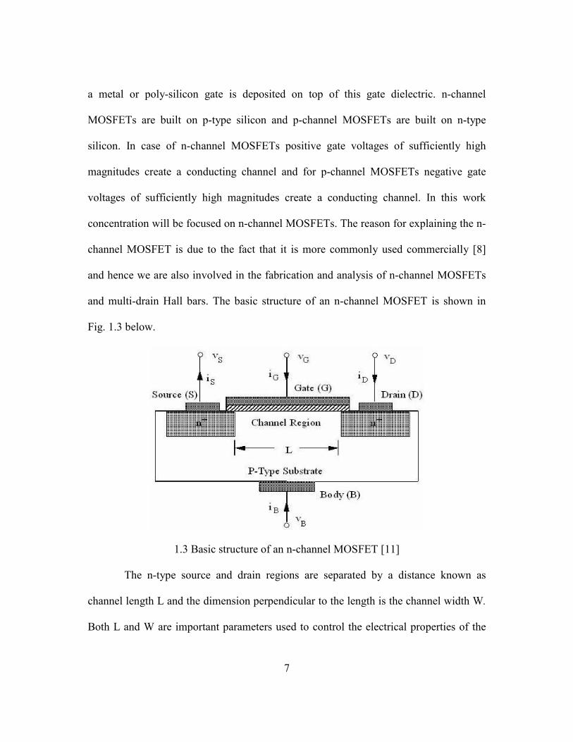
7
a metal or poly-silicon gate is deposited on top of this gate dielectric. n-channel
MOSFETs are built on p-type silicon and p-channel MOSFETs are built on n-type
silicon. In case of n-channel MOSFETs positive gate voltages of sufficiently high
magnitudes create a conducting channel and for p-channel MOSFETs negative gate
voltages of sufficiently high magnitudes create a conducting channel. In this work
concentration will be focused on n-channel MOSFETs. The reason for explaining the n-
channel MOSFET is due to the fact that it is more commonly used commercially [8]
and hence we are also involved in the fabrication and analysis of n-channel MOSFETs
and multi-drain Hall bars. The basic structure of an n-channel MOSFET is shown in
Fig. 1.3 below.
1.3 Basic structure of an n-channel MOSFET [11]
The n-type source and drain regions are separated by a distance known as
channel length L and the dimension perpendicular to the length is the channel width W.
Both L and W are important parameters used to control the electrical properties of the

8
MOSFET [8]. The thickness of oxide oxx covering the channel area just below the gate
is a very important parameter too. The source and drain regions are electrically
disconnected unless there is a conducting channel between them. This conducting
channel is provided by the n-type inversion layer which is formed by the application of
the gate voltage. When the inversion layer is formed and a voltage is applied between
the source and drain regions, the carriers enter the channel from the source and depart
from the drain, which results in current from drain to source in case of n-channel
MOSFETs and source to drain in case of p-channel MOSFETs. We can fabricate the
MOSFETs, which have an inversion layer at zero gate-to-source voltage (Vgs). These
kinds of MOSFETs are called depletion-mode MOSFETs. The drain current in these
MOSFETs can be reduced by changing the gate-to-source voltage (Vgs). MOSFETs in
which inversion layer is not formed at Vgs = 0 are called enhancement-mode MOSFETs.
Enhancement–mode MOSFETs are more commonly used in circuits than depletion-
mode MOSFETs [8, 9].
1.2.2 The MOS system under External Bias-Operating Modes of a MOSFET
There can be two controlling parameters for MOSFET operation. These are gate
voltage (Vg) and substrate voltage (Vb). In the analysis of electrical behavior of the
MOSFET substrate voltage Vb = 0 and the gate voltage Vg is the controlling parameter.
With the polarity and magnitude of the gate voltage Vg three operating regions are
observed in a MOSFET i.e. accumulation, depletion and inversion. We concentrate our
analysis on n-channel MOSFETs here.

9
On application of negative gate voltage Vg, the holes, that are the majority
carriers in the p-type substrate, come to the semiconductor-oxide interface. The
majority carrier concentration near the surface exceeds the equilibrium concentration of
majority carriers i.e. the holes in the substrate and this condition is knows as
accumulation as this is caused by the carrier accumulation on the surface [8, 9]. The
applied negative surface potential causes the energy bands to bend upward near the
surface. This is demonstrated in the Figure 1.4 below. Due to the applied negative
voltage the concentration of the holes increase near the surface but the concentration of
the electrons decreases near the surface as the electrons are pushed deeper into the bulk
of the substrate [8, 9].
Figure 1.4 Energy band diagram of MOS system operating in accumulation [8]
When a small positive gate voltage Vg is applied and the substrate bias being
Vb=0, the electric field is directed towards the substrate in this case and hence the holes,
which are the majority carriers, are pushed back into the substrate leaving behind
negatively charged fixed acceptor ions. A depletion region is created near the surface

10
and the semiconductor-oxide interface is devoid of any mobile carriers. This is known
as the depletion region of operation of a MOSFET. The positive gate bias causes the
energy bands to bend downwards near the surface. This is demonstrated in the energy
band diagram of depletion region operation in Fig. 1.5 below [8, 9].
Figure 1.5 a) Energy band diagram of a MOS system operating in depletion
b) Cross-sectional view of MOS system operating in depletion [8]
The thickness of the depletion region is expressed as a function of the surface
potential and bulk Fermi potential as
A
FsSi
dNq
x.
..2 φφε −= (1.2)
And the depletion charge density is given as
FsSiANqQ φφε −−= ...2 (1.3)

11
Where dx is the depth of the depletion region, Q is the depletion region charge
density, sφ is the surface potential, Fφ is the bulk Fermi potential, AN is the acceptor
concentration and Siε is the dielectric coefficient of silicon [8].
If the positive gate bias is increased further the electrons from the bulk are
attracted towards the surface and the electron density exceeds the majority hole density.
As a result of this an n-type region is created near the surface and it is called the
inversion layer and this phenomenon is called surface inversion. As a result of
increasing surface potential the energy bands bend further downwards and eventually
the mid-gap energy level iE gets smaller than the Fermi level FpE on the surface
concluding that the substrate semiconductor in this region becomes n-type. This is
demonstrated in the energy band diagram shown below.
Figure 1.6 Energy band diagram of a MOS system operating in inversion
b) Cross-sectional view of MOS system operating in inversion [8]

12
This inversion condition requires that the surface potential sφ has the same
magnitude but different polarity as the bulk Fermi level Fφ [8, 9]. On reaching the
condition of surface inversion, there is no further increase in the depth of the depletion
region. After that with the increase of the positive gate bias, only the mobile electron
concentration increases. So the depletion region depth achieved at the onset of inversion
is the maximum depth of the depletion layer [8]. With inversion condition sφ = - Fφ the
maximum depth of depletion layer is given by
=dmxA
FSi
Nq.
2..2 φε (1.4)
Where dmx is the maximum depth of depletion layer [8].
1.2.3 Threshold Voltage
The value of gate-to-source voltage Vg needed to cause surface inversion
condition is called the threshold voltage VT0. So Vg > VT0 for the conductance in the
channel to take place. Threshold voltage is a very important parameter in the operation
of MOSFET. As mentioned earlier at the onset of inversion sφ = - Fφ so modifying
equation (1.3) to use this condition [8]:
FSiAB NqQ φε 2...20 −−= (1.5)
But as the source is at a different potential than the substrate, the depletion
region charge density can be expressed a function of source to substrate voltage Vsb.
sbFSiAB VNqQ +−−= φε 2...2 (1.6)

13
The component that offsets the depletion region charge is ox
B
C
Q− where oxC the
capacitance of the gate oxide per unit area is given as
ox
ox
oxt
Cε
= (1.7)
There is always a fixed positive charge density oxQ at the interface between gate
oxide and the silicon substrate due to impurities and lattice imperfections. The gate
voltage component to offset this component isox
ox
C
Q−[8]. Combining all these factors the
threshold voltage for zero substrate bias is given as
ox
ox
ox
B
FGCTC
Q
C
QV −−−= 0
0 2φφ (1.8)
But VT0 is the threshold voltage for in case of zero-substrate bias. For threshold
voltage in case of non-zero substrate bias
ox
ox
ox
BFGCT
C
Q
C
QV −−−= φφ 2 (1.9)
The final expression of threshold voltage [8] that is considered most widely is
given as
( )FSBFTT VVV φφγ 22.0 −+−+= (1.10)
Where the parameter γ is known as the substrate bias coefficient [8] and is
given as
ox
SiA
C
Nq εγ
..2= (1.11)

14
The threshold voltage expression given in Eq. (1.10) can be used for both
nMOS and pMOS devices. The difference would be the polarity in case of some of the
perimeters. Specifically
• Fφ is negative in case of n-channel MOSFETS, positive in p-channel
• 0BQ and BQ are negative in n-channel MOSFETs, positive in p-channel
• γ is positive in n-channel MOSFETs, negative in p-channel
• sbV is positive for n-channel MOSFETs, negative for p-channel
But typically the threshold voltage is negative for p-channel MOSFETs and
positive for n-channel MOSFETs [8, 9].
1.2.4 Gate Oxide
The thickness and the quality of the gate oxide are two of the most critical
parameters, as these qualities strongly affect the operational characteristics of a
transistor and also its long-term reliability [8, 9]. It can be recollected that the drain
current [9] of a MOS transistor can be given by:
( )Tgsdsoxd VVVfL
WCI ,,..µ= (1.12)
where µ is the mobility of electrons in nMOS,
oxoxox xC ε= is the gate oxide capacitance per unit area,
W/L is the ratio of channel width to channel length and
VT is the threshold voltage of the transistor.
The above equation clearly indicates that the drain current is directly proportional to the
gate oxide capacitance per unit area, which is inversely proportional to the gate oxide

15
layer thickness xox. Thus random fluctuations in xox can cause the corresponding
variation in the drain current even under the same biasing conditions. These variations
in the drain current can cause the variations in the circuit performances such as delay
times, power consumption and logic threshold voltage [8, 9]. The function of the gate
oxide is to provide a high-quality insulator between the conductive gate and the
substrate. Although it prevents the current flow from the gate to the substrate, the oxide
layer allows the penetration of electric field from gate to the substrate. The gate oxide in
the MOS transistors is usually silicon dioxide SiO2 or it can be Silicon Oxy-nitride
SiON or silicon nitride Si3N4 [4].
1.2.5 Carrier Mobility and Current Density
Carrier mobility (µ) is an important parameter in determining device
performance in electronics. It is vital for describing the operation of semiconductor
devices such as a MOS transistor [12]. It is one of the important input parameters for
expressing electrical current in devices. The knowledge of carrier mobility is also
important for knowing the doping level in wafers [12]. Here by carrier mobility we
mean the electron mobility µn and hole mobility µp. As electrons are the majority
carriers in nMOS devices, we are inclined towards the electron mobility analysis.
Mobility is an important parameter for carrier transport as it describes how strong the
motion of an electron or a hole is influenced by an applied electric field.
The electrons (or holes) in a semiconductor move rapidly in all directions at
room temperature [13, 14]. In the absence of an applied electric field, the carrier
exhibits random motion and carriers move quickly through the semiconductor and

16
frequently changes direction. When an electric field is applied, the random motion still
occurs but in addition to that, there is on an average motion along the direction of the
field. Due to their different electronic charge, holes move on in the direction of the
electric field while electrons move in the opposite direction [13]. This phenomenon is
shown is Fig. 1.7 below
Figure 1.7 Random motion of carriers in a semiconductor with and
without applied electric field [13].
The random motion of electrons leads to zero net displacement of an electron
over a sufficiently long period of time. The average distance between collisions is called
the mean free path and the average time between collisions is called the mean free time
(τc). For the typical value of 5101 −× cm mean free path, the mean free time(τc) is about
1 ps (~ 10-12
s) [14]. On application of a small electric field (E) on the semiconductor
sample, each electron experiences a force –qE along the field (in the opposite direction
of the field) between collisions. Hence an additional velocity component is
superimposed upon the thermal motion of electrons called drift velocity (vn). So the net
displacement of the electrons is in the direction opposite to applied field due to
combined effect of drift velocity and random thermal motion. The electron drift velocity

17
is proportional to the applied electric field. The proportionality factor depends on the
mean free time and the effective mass. This proportionality factor is the electron
mobility (or hole mobility) in the units of cm2/V-s given as [14]
*m
q c
n
τµ = (1.13)
where µn is the electron mobility,
q is the charge on a electron,
τc is the mean free time and
m* is the effective mass of the electron.
Hence
Ev nn .µ−= (1.14)
where vn is the drift velocity of the electrons. The negative sign is used in the Eq. (1.14)
as the electrons drift in the direction opposite to the Electric field E. A similar
expression for hole mobility is given by
Ev pp .µ= (1.15)
where vp is the drift velocity of the holes, µp is the hole mobility and E is the applied
electric field. The negative sign is not incorporated in the equation as the holes drift in
the same direction as the electric field [14].
The current density (J) at low fields [14] due to conduction by drift therefore
can be written in terms of electron and hole drift velocities, vn and vp as
pn vpqvnqJ .... += (1.16)

18
At high fields scattering limits the velocity to the maximum value and the relationship
given above ceases to hold any importance. This is termed as velocity saturation [14].
The expression for J in terms of mobility µ can be written as
( )EpqnqJ pn ..... µµ += (1.17)
The first term in the above expression is the conductivity σ, in ( ) 1−Ωcm and it is the
inverse of the resistivity ρ [8]. So the above expression can be written in the form of
conductivity and resistivity as
( )EEJ .1. ρσ == (1.18)
1.3 Channel Mobility Degradation Mechanisms in a MOSFET
The inversion layer mobility in MOSFETs has been a very important physical
quantity that is a parameter used to describe the drain current and a probe to study the
electrical properties of the two-dimensional carrier system [15]. But a comprehensive
understanding of inversion layer mobility, which includes the quantitative description
near room temperature, the effect of substrate doping, the difference between electron
and hole mobility and the effect of surface orientation is of paramount importance.
Takagi et. al describe effective normal field by the equation [15]
( )( )sdpSieff NNqE ./ 1 ηε += (1.19)
where q is the elementary charge, εSi is the permitivity of silicon, Ndp1 is the surface
orientation of the depletion charge, Ns is the surface inversion carrier concentration.
Here η is the key parameter in defining the effective normal field and in order to

19
provide a universal relationship, the value of η should be ½ for electron mobility and
1/3 for hole mobility. Effective normal field can also be expressed as
( )Binv
Si
ff QQE += .1
ηε
(1.20)
where εSi is the permitivity of silicon, Qinv is the inversion layer charge and QB is the
bulk depletion layer charge [16]. There are various factors that influence inversion layer
mobility of carriers in a MOS transistor which include temperature, surface roughness,
oxide quality and surface orientation of the Silicon wafer [15, 17]. With the scaling
there is reduction in inversion layer mobility and this further reduces the current
density. The various mechanisms responsible for the degradation in inversion layer
mobility will be discussed in detail in the sections 1.3.1 and 1.3.2.
1.3.1 Charge Scattering Mechanisms
There are several scattering mechanisms inherent in the gate oxide. Scattering
of inversion layer electrons (in n-MOS) at the oxide semiconductor interface is one the
major source of mobility degradation in MOSFETs [18]. The relative importance of the
scattering mechanisms depends on the operating temperature and strength of the surface
electric field. According to equation B the mobility of electrons in the inversion layer is
given by
*m
q c
n
τµ = (1.21)
where µn is the electron mobility, q is the charge on a electron, τc is the mean free time
and m* is the effective mass of the electron [14]. So the mobility is directly related to

20
mean free time between collisions, which in turn is determined by the scattering
mechanisms [14]. Some of the main scattering mechanisms are discussed here.
A) Phonon Scattering: Lattice scattering is a result of the thermal vibrations of the
lattice atoms at any temperature above the room temperature. The lattice periodic
potential is disturbed by these vibrations and it allows the energy to be transferred
between the lattice and the carriers. With increase in the temperature the lattice
vibration increases. Consequently lattice scattering becomes dominant at high
temperatures, thereby reducing the mobility at higher temperatures [14]. The allowed
vibrational motions, which interact with the free electrons, are termed phonons.
Scattering by acoustic phonon is called the phonon scattering and is found to limit the
mobility in semiconductors at room temperatures. This scattering increases with the
increase in the temperature. The acoustic phonons have the energies of approximately
0.05 eV. The mobility due to acoustical phonon scattering µL decreases with increase in
temperature as 23−T [14, 19]. So phonon scattering is important at room temperature and
can be ignored at very low temperatures [19].
From Eq. (1.21) it can be observed that carrier mobility is inversely
proportional to the effective mass. Hence, a larger mobility is expected with a carrier
with smaller effective mass. Electron effective mass is smaller than the hole effective
mass pn mm ** < [12]. At a given impurity concentration, the electron mobility exceeds
the hole mobility pn µµ > [12, 14]. This is demonstrated in the Fig. 1.8.

21
Figure 1.8 Electron and hole mobility versus doping density for silicon [13]
B) Coulomb Scattering: Ionized impurity scattering occurs when a charge carrier travels
past an ionized dopant impurity, either a donor or an acceptor. The charge carrier path
will be deflected due to Coulomb force interaction. The probability of impurity
scattering depends on the total concentration of the ionized impurities, which is the sum
of the concentration of negatively and positively charged ions. So as the Coulomb
interaction is involved here, hence the name Coulomb scattering [14]. Coulomb
scattering is basically due to charge centers, including fixed oxide charges, interface
state charges and localized charge due to ionized impurities [19, 20]. Along with the
Coulomb scattering these charges also have trapping effects [12, 14], which will be
discussed in detail in the next section. The Coulomb scattering by substrate impurity is
considered to degrade the mobility on higher impurity concentration substrates [15, 21].
However, unlike lattice scattering, impurity scattering becomes less a significant at

22
higher temperatures. This is because of the reason that the carriers move rapidly at
higher temperatures and remain near the impurity center for a very short time. Hence
there is less time for the Coulomb interaction to take place. This reduces the Coulomb
scattering at higher temperature. The mobility near the room temperature due to ionized
impurity scattering or Coulomb scattering varies with temperature and ionized impurity
concentration NI . This is given as INT /23 . So Coulomb scattering is an important
consideration at lightly inverted surfaces. High surface charge densities or substrate
doping concentration imply increase in Coulomb scattering. Coulomb scattering
becomes less effective at heavily inverted surfaces due to carrier screening [19].
C) Surface roughness scattering: This scattering mechanism refers to the roughness at
the Si-SiO2 interface [19, 22, 24]. Popular analysis of surface roughness scattering
suggests usually assume that mobility due to surface roughness scattering is temperature
independent [15]. But from a physical standpoint carrier screening is supposed to give it
some temperature dependence [23]. The mobility due to surface roughness scattering
varies with temperature as T –1/3
. Surface roughness has the maximum impact on the
mobility at low temperatures. The surface roughness scattering is important under
strong inversion conditions as the distance of carriers from the surface governs the
strength of the interaction. The closer the carriers are to the surface, the stronger the
scattering due to surface roughness will be [19, 25].

23
Figure 1.9 Temperature dependence of the surface roughness limited mobility
[23]
The total mobility is usually assumed to be related in a reciprocal manner to the
individual contributions as
srcph µµµµ1111
++= (1.22)
where µph is the mobility due to phonons, µc is the mobility due to coulomb scattering
and µsr is the mobility due to surface roughness [16].
1.3.2 Charge Trapping Mechanisms
The understanding of the influence of charge within the oxide and at the oxide-
silicon interface is very important. The presence of these charges is unavoidable in
practical systems. These charges can cause various changes in the characteristics of the
device, most importantly altering the threshold voltage and the flatband voltage [9]. In

24
some cases the applied voltage influences these charges. In this case the threshold
voltage depends on the gate voltage. The capacitance-voltage curve is then distorted as
shown in the figure below.
Figure 1.10 Fixed charge effects on the capacitance-voltage curve of a
MOS system [9]
There are four distinct types of charges in the oxide-Silicon system. These
four different types of charges are shown below in Fig. 1.11 below. These charges are
located on different locations of the oxide-silicon system.
Figure 1.11 Four categories of oxide charges in a MOS system [9]
25
A) Interface trapped charge: This is a positive charge and is located in a very thin
(<1 nm) transition layer of non-stoichiometric silicon oxide SiOx. The trapping levels
are located at the oxide-silicon interface and have the energy levels within the forbidden
gap between the valence band and the conduction band. They are distributed over
energies within the energy gap. Clean surfaces have extra-allowed energy levels
different from those in the bulk of the crystal. The inevitable presence of crystal defects
and impurities introduced during processing add to more energy levels. Electrons in
these extra levels and ions associated with them contribute to the interface charge[9].
The density of interface trapping states can be reduced typically by annealing the
oxidized silicon wafer in hydrogen or forming gas [9, 25].
B) Fixed Oxide charge: The fixed charge is present at the interface and within the
oxide. The fixed charge always present at the interface arises from incomplete Si-Si
bonds. The density of atoms at the surface of the silicon crystal depends on the crystal
orientation and therefore depends on the orientation of the wafer [9, 17]. As more bonds
are broken in the transition from silicon wafer with orientation (111) to silicon dioxide
than in the transition in case of a (100) silicon wafer, fixed charge density is higher
when (111) is used. Due to this reason the all the commercial devices are fabricated on
(100) and not (111) [17]. Fixed charge densities also depend on high temperature
processing hence annealing at high temperature can reduce some bonds and reduce the
fixed charge density [9]. Fixed charge at the interface and within the oxide changes the
threshold voltage [26]. So high fixed charge densities can cause the threshold voltage to
be very high for practical applications especially with reduced supply voltage. In most

26
practical MOS structures, the densities of other charge centers, like the interface-
trapped charge, are much smaller than the fixed oxide charge densities [19]. For
example interface states commonly exhibit densities at least an order of magnitude
smaller than fixed charge densities, provided an appropriate thermal anneal (generally
400-500oC in an N2 or N2/H2 ambient) in the fabrication sequence[19, 27].
C) Mobile ionic charge: These charges result from alkali-metal ions (like sodium and
potassium) that are readily absorbed in silicon dioxide. The alkali ions are sufficiently
mobile to drift in the oxide in low voltage application. Their stability increases with
increasing temperature so their effect on flatband voltage is more severe on high
temperatures [9]. As the metal ions are positively charges, negative gate voltage causes
the ions to migrate in to the metal-oxide interface where they do not affect the flatband
voltage. But positive gate voltage moves these charges to the oxide-silicon interface
where their effect is maximum. These charges can be avoided by careful processing and
by introduction of certain impurities that immobilize these impurities [28]. Some of
these impurities that can immobilize these ionic charges are chlorine and chlorine
compounds which can be introduced by processing to stabilize the MOS system [9, 28].
D) Oxide trapped charges: These charges are located in the traps distributed throughout
the oxide layer. Only a small amount of oxide trapped charges are introduced during
processing. This charge is fixed except under unusual conditions. These charges can be
both positive and negative but are usually negative [9].

27
1.4 High-K Dielectric Materials as an Alternative to SiO2
For more than 15 years, the physical thickness of SiO2 has been reduced
aggressively in compliance with Moore’s law for low power consumption, high
performance CMOS applications [29]. This is because it requires high integrated circuit
density, which has translated into higher density of transistors on the wafer [30]. The
improved performance related with the scaling of the device dimensions can be
associated with the following equation [30] as
( )[ ]20.2..2
.dsdsTgs
oxnD VVVV
L
WCI −−=
µ (1.23)
where W is the width of the transistor channel, L is the length of the transistor channel,
µn is the mobility of carrier electron in the channel, Cox is the capacitance density
associated with the gate dielectric when underlying channel is in the inverted state, Vgs
and Vds are voltages applied to transistor gate and drain and VT0 is the threshold voltage
[30]. The drain current Id increases linearly with Vd and eventually saturates at Vdsat. To
yield drain current as
( )20..2
.)( Tgs
oxnD VV
L
WCsatI −=
µ (1.24)
The term Vg-VT0 is limited in the range of reliability and room operation
constraints as Vg cannot be very high. Thus even in a simplified approximation,
reduction in channel length or an increase in the gate dielectric capacitance can increase
drain current Idsat. One of the key elements that have allowed the successful scaling of
SiO2 is its excellent material and electrical properties like thickness uniformity and
control growth with a low density of interface defects, excellent chemical and thermal

28
stability and large band gap which confers excellent isolation properties for it. But
scaling beyond the present 1.2 nm range is an impediment in device scaling [31]. The
first problem is the leakage current. This is because when the gate dielectric is very thin,
the charge carriers can flow right through the gate insulator and this is called the
quantum mechanical tunneling effect [31, 32]. This tunneling probability increases
exponentially with the reduction in the thickness of the gate insulator. This results into
an increase in the leakage current. Another issue can be the device reliability, as during
the device operation carriers flow through the device, resulting in defects in the SiO2
layer and the Si-SiO2 interface. This can result in the breakdown of the dielectric and
eventual breakdown of the device. Moreover the maximum gate voltage that can be
applied to the device reduces with the thickness of the SiO2 layer [33]. As temperature
is increases some of the defect densities can increase high enough to cause a
breakdown. All these limitations have prompted research for alternate gate dielectric
materials, which can compensate for the scaling effects and help in the further scaling
of the devices [30, 33].
If we just consider the gate capacitance, which is given as x
AC
.. 0εκ= where k
is the dielectric constant, ε0 is the permittivity of free space, A is the area of the
capacitor and x is the thickness of the gate dielectric. The expression of C can be written
in terms of xeq and kox, which are the equivalent oxide thickness and dielectric constant
of the capacitor respectively. xeq is the thickness of SiO2 that would be required to
achieve the same capacitance density as the dielectric. So the physical thickness of an
29
alternative dielectric employed to achieve the equivalent capacitive density of xeq can be
obtained from the expression [33]
eq
ox
high
high xxκ
κ κκ
−− = (1.25)
So a gate dielectric with a higher dielectric constant affords a greater physical
thickness and achieves the same capacitance as achieved by SiO2 with lesser thickness.
In other words by using high-k gate dielectric we can employ a thicker gate layer with
lesser equivalent oxide thickness [30, 32, 33].
Figure 1.12 High-k for gate dielectrics [3]
Currently a wide range of materials are being investigated as an alternative to
SiO2 as gate dielectric material. Most of these materials are titanium (Ti) based e.g.
TiO2 [34], TiSixOy [35], zirconium (Zr) based e.g. ZrO2 [33, 34], hafnium (Hf) based
e.g. HfO2 [33, 34, 36, 37], HfSixOy [35, 36, 38] and aluminum (Al) based e.g. Al2O3
[34, 36]. The dielectric constants for these materials range from 9 (Al2O3) to 80 (TiO2)

30
[31]. There is also ultra high gate dielectric SrTiO3 that has a dielectric constant 200
[31]. But it is not being investigated for the use in commercial devices. The dielectric
constant of HfSixOy is equal 8-15 depending upon the composition of Hafnium in the
compound [31, 39].
Several methods of deposition are being investigated for the deposition of high-
k materials on silicon. Plasma vapor deposition of HfO2 followed by forming gas anneal
[36], Atomic layer chemical vapor deposition using HfCl4 and H2O and metal organic
chemical vapor deposition of HfO2 and HfSixOy [33, 40], low temperature deposition of
HfSixOy by sputtering [39] and vapor-liquid hybrid deposition of Hafnium silicate films
using Hf(OC4H9) and Si(OC2H5)4 [41] are some of the methods that have been reported.
The high-k materials being investigated, though very promising, should fulfill
some of the criteria that are important to their implementation as gate dielectric. Some
of these criteria like permittivity, band structure and offset, thermodynamic stability,
interface quality, film morphology, gate electrode compatibility, process compatibility
and reliability should be addressed [42]. Fig. 1.13 demonstrates the conduction band
and valence band offsets of various oxides on silicon.

31
Figure 1.13 Conduction band and valence band offsets of various oxides on
Silicon [42]
Most importantly the high-k dielectric materials are required to meet the gate
leakage requirements. Therefore the focus of efforts has shifted to Hafnium and
Aluminum based dielectrics [33, 37]. These materials have the required thermodynamic
and physical stability required for the integration with silicon substrate and
metal/polysilicon gate during processing [37, 43]. Hafnium Silicate (HfSixOy) is one
potential candidate along with Hafnium oxide (HfO2) [39, 44]. Out of these two, HfO2
has been a subject of very intense research. For thin gate dielectric candidates, the
interface with the silicon channel plays a very important role in determining overall
electrical properties. The thermal stability of refractory metal oxides such as TiO2 has
been investigated but they are not stable in contact with silicon and thus require an
interfacial layer [34]. Though interface barriers have been developed between high-k
and the silicon substrate, they comprise the gate stack capacitance since SiO2 limits the

32
total capacitance of the stack. While HfO2 has high dielectric constant [45] and is
thermodynamically stable next to silicon under equilibrium conditions, interfacial
reactions occur which produce materials with lower k such as SiO2 or silicate thereby
seriously diminishing the total capacitance. Also, HfO2 and ZrO2 tend to crystallize at
relatively low temperature, leading to the formation to poly-crystalline films, with
enhanced leakage current paths along the grain boundaries [38, 45]. HfO2 is an ionic
conductor, as O ions can diffuse through the oxides and leave vacancies behind which
can act as traps and reliability concerns [45]. So to prevent these shortcomings in the
oxide dielectrics HfSixOy is used. HfSixOy is also stable in direct use with silicon, and
by incorporating a sufficiently high level of Silicon during deposition, the dielectric-Si
interface will act more like the preferable SiO2-Si interface, and the driving force is
removed for any reaction between the substrate and the dielectric [46]. Use of HfSixOy
allows the control of silicon interface and also affords the significant flexibility for the
use of poly-silicon gate [45]. Moreover HfSixOy remains amorphous at temperatures
greater than 900oC. So though HfSiO has a dielectric constant K=11 with 6% Hf, [38]
they have some characteristics that are better than HfO2 and hence can be used a gate
dielectric. HfSixOy dielectric materials have better leakage characteristics, improved
threshold voltage characteristics, lower mobility degradation and allow larger thermal
budgets during processing than HfO2 [47]. Due to this reason we have chosen HfSixOy
as gate dielectric material in our process. HfSixOy films (with smaller k compared to
HfO2 and phonon energy larger than HfO2) as gate insulator show mobility closer to the
SiO2 based devices. The HfSixOy based devices may provide sufficient gate leakage

33
reduction at desired electrical oxide thickness without too much loss of carrier mobility
[48].
Though high-k dielectric materials look very promising, there are certain
challenges that have to be met before successful transition from SiO2 to high-k. Among
them some are noteworthy. First problem is with replacing polySi/SiO2 stack with
polySi/high-k stack. Due Fermi level pinning at the polySi/high-k interface, high-k
dielectrics and polySi are incompatible. The Fermi level pinning is most likely caused
by defect formation at the polySi/high-k interface [29, 33, 49]. This causes high
threshold voltages in high-k transistors.
Figure 1.14 Defect formation at the poly-Si and high-k dielectric interface
[29]
Apart from the problem of high threshold voltage, presence of electrical
instabilities of the threshold voltage in the electrical performance of high-k transistors is
another problem which seriously comprises the performance and long term operation of
the device. They cause hysteresis in the Id Vs VG characteristics when ramping the gate
voltage up and down [33, 37]. Long term reliability and expected lifetime of the high-k

34
stacks are important issues. Issues like Stress induced leakage current (SILC) generation
[33], time dependent dielectric breakdown (TDDB)[33, 37] and negative bias
temperature instability (NBTI) [33, 37] are being investigated. But the most important
issue with the high-k gate dielectric material is the mobility degradation. This is
discussed in detail in the subsequent section.
1.5 Mobility Degradation in High-K Dielectric Materials
The most challenging problem for the high-k dielectrics in the present scenario
is the transistor drive performance, which is directly linked to the carrier mobility in the
channel [33]. Several factors can limit the inversion channel mobility in the transistors
with high-k gate dielectric material. The scattering mechanisms like Coulomb
scattering, soft phonon scattering and surface roughness scattering, and charge trapping
contribute to the mobility degradation. Along with that, the thickness and material
quality of the interfacial oxide layer can also influence the results [48]. It is found that
high-k layers demonstrate lower mobility than conventional SiO2. The problem is more
severe for n-channel than for p-channel devices [33]. The materials with largest k values
show the poorest mobility because of the correlation between mode energy and
amplitude and the k value [48].
Coulomb scattering due to high density of interface trapped charges and fixed
oxide charges appears to be an important contributor [50, 51]. It was observed that
higher the interface trap density, lower the mobility. The interface trap density near the
conduction band is higher than that near the valence band. Consequently degradation in
hole mobility in p-MOS is less then electron mobility in n-MOS [52]. Coulomb

35
scattering dominates at low field regime [48]. The low mobility values in the high-k
gate stacks as well as its dependence on interfacial oxide thickness can be explained by
assuming that Coulomb potential is responsible for scattering of electrons [48]. The Fig.
1.15 demonstrates the reduction in maximum mobility with decreasing interfacial oxide
thickness. The solid symbols denote metal gates and open symbols denote poly-Si gates
[33].
Figure 1.15 Reduction in maximum mobility with decreasing thickness of
interfacial oxide. [33]
The high-k dielectrics can suffer from severely degraded mobility due to the
coupling of low energy surface optical phonons which arise from the polarization of the
high-k dielectric to the inversion channel charge carriers [29, 31]. The scattering by
phonons limits inversion layer electron mobility at the medium field regime and low
lattice temperatures [48]. Mobility due to soft optical phonons in high-k was found to be
significantly lower than its SiO2 counterpart. This indicates severe phonon scattering for
the former [52]. It was indicated that mobility degradation in high-k dielectric materials

36
is intrinsic and is related to scattering by soft phonons. Severe mobility degradation due
to phonon scattering was reported in high-k/polySi stacks as compared to SiO2/polySi
stacks [48, 53, 54].
The lower mobilities are also due to aggressive interfacial oxide thickness used
for these stacks. The peak mobility in n-MOS devices with high-k layer is observed to
increase along the thickness of the interfacial SiO2 or SiON. This proves that the
scattering mechanism that reduces the mobility becomes less important when the high-k
is further away from the channel. So it is very vital to specify the thickness of the
interfacial oxide when comparing values of mobilities from different gate stacks [33,
55].
All the high-k materials contain large amounts of fixed charges compared to
SiO2, independent of the high-k film deposition technique. The charge trapping centers
responsible for the fixed charges are likely to be in the bulk of the high-k film and at the
interfaces of the high layer with the gate electrode and the interfacial layer [37]. The
presence of trapped charges impact the conduction mechanism. Depending upon the
position of the trap centers and the barrier heights at the gate at the silicon substrate,
defect related tunneling mechanisms may be important. The dominant conduction
mechanism may be process, voltage or polarity related [37, 47]. The fixed charge within
the high-k film causes the shift in the threshold voltage VT and poses serious problems
with the threshold voltage control along with diminishing the mobility. Process
integration focused to minimize the fixed charge includes post deposition anneals and
optimization of the interfacial layer. [37, 47, 56].

37
1.6 Methods of Mobility Extraction
1.6.1 The Hall Effect
The Hall Effect describes the behavior of the free carriers in a semiconductor
when applying an electric as well as magnetic field. An experimental setup shown in
Fig. 1.16 below demonstrates a semiconductor bar with rectangular cross section and
length L.
Figure 1.16 Hall setup and carrier motion for a) holes b) electrons [57]
A voltage Vx is applied between the two contacts resulting in the field in the x-
direction. The magnetic field is applied in the z-direction [57]. When an electron moves
along a direction perpendicular to the applied magnetic field B (also termed H), it
experiences force acting parallel to both directions and moves in response to this force
and the force effected by the internal electric field. The behavior of holes is shown in
Fig. 1.16(a) and the behavior of electrons is shown in Fig. 1.16(b). The electrons travel
in the negative x-direction. Therefore the force Fy is in the positive y-direction due to
the negative charge and the electrons move to the right. In steady state this force is
balanced by an electric field Ey so that there is no net force on the electrons. As a result

38
there is a voltage across the sample, which can be measured by a high impedance
voltmeter. This voltage is called the Hall voltage and it is negative for the electrons
given the sign convention [57]. The Lorentz force acting on the free carriers [57] is
given by
(1.26)
When both electrons and holes are present in the same sample, both charge
carriers experience Lorentz force in the same direction since they would be drifting in
the opposite direction as shown in the Fig. 1.17 below. The figure below shows that the
magnetic field Bz is out of the plane of the paper. Both electron and holes are deflected
towards the bottom surface of the conductor and consequently the Hall voltage depends
on the relative mobilities of the electrons and holes and also the concentrations of
electrons and holes in the conductor [58, 59].
Figure 1.17 Hall Effect for ambipolar conduction in a semiconductor with
both electrons and holes [58]

39
Our Hall analysis is not on a ambipolar conduction but on a unipolar
conduction. The Hall field is the electric field developed across the two faces of a
conductor, in the direction Bj × where j is the current that flows across a magnetic field
B [59]. We assume that the carriers in Fig. 1.17 can only flow along the x-direction and
their velocity is vx. The Lorentz force then becomes
( ) zzyzxyxx eqEeBvEqeqEF→→→→
+−+= (1.27)
Since the carriers only flow along the x-direction, the net force must be zero
along the y and z directions. As a result the electric field is zero along the z-direction
( ) 0=−=→
zxyy BvEqF (1.28)
which gives a relation between the electric field along the y-direction and the applied
magnetic field, which can be expressed as a function of current density as follows:
z
n
x
zxy Bqn
JBvE −=−= (1.29)
This electric field is called the Hall field [58]. The Hall coefficient can be defined as
Hall field divided by the applied current density and magnetic field:
nzx
y
HqnBJ
ER
1−== (1.30)
The negative sign in the above equation is for free electrons. It will be positive for
holes. The lower the carrier concentration, the greater the magnitude of the Hall
coefficient. Measuring RH is an important way of measuring carrier concentration [59].
The Hall coefficient can also be measured from the measured current Ix and the
measured voltage VH [59].

40
The measurement of Hall voltage is important to measure various parameters
like type of semiconductor and free carrier density. But the most important application
of Hall voltage measurements is to find out the carrier mobility in the inversion layer.
Since the measurement can be done on a small piece of uniformly doped sample, it is a
very convenient and accurate method of measuring carrier mobility. But the scattering
mechanisms in the channel in the presence of magnetic field are different and the Hall
mobility can be different from true drift mobility [28, 59]. The reason for doing Hall
measurements is that split-capacitance can’t distinguish between mobile a trapped
charge, while Hall Effect see only mobile charge. So we can, in principle get mobility
from Hall measurements even when there is a lot of trapping. For this we need to find
the Hall factor r. I am proposing that we measure magnetoresistance, because theory
indicates some correlation of r with it. We can measure the true drift mobility with the
combination of Hall voltage and magneto-resistance measurements. We know that µH =
rH×µD, where µH is the Hall mobility, rH is the Hall factor and µD is the drift mobility.
Hall mobility can be calculated from Hall voltage measurements using specially
designed multi-drain transistors, Hall factor, which is considered to be ranging from 1
to 2 can be calculated using the magnetoresistance calculations and with the help of
these two parameters the true drift mobility can be found out. The Hall factor is
considered to be ~1, which means that Hall mobility is equal to the drift mobility [52].
We aim at improving the accuracy of the Hall factor and thereby finding the true drift
mobility.

41
1.6.2 Split C-V Measurements
Split C-V measurement technique is widely used in the mobility extraction in
MOSFETs. It is considered to be a very accurate measurement technique [60, 61]. The
difference in this method, in comparison to with the low frequency CV method is the
separate measurement of the bulk and source-drain contributions to the gate capacitance
C as a function of gate voltage Vg of a MOS transistor [62]. At the root of the
application of the split CV measurement method lies the supposition that the MOS
transistor should meet the requirement that in the inversion condition of the surface of
the silicon,
a) The small signal excess majority charge is supplied by a bulk hole current and
b) the interface state charge as well as the excess minority carrier charge is supplied by
an electron current which originates from the source drain diffused regions [62].
The split C-V measurement technique can help find the charge trapped in
interface states and interface state densities in weak inversion. [62]. Experimentally
effective mobility can be approximated using the expression [60]
( ) nds
d
QVLW
I='µ (1.31)
where Id is the drain current, W, L are the channel width and length respectively, Vds is
the drain voltage and Qn is the absolute value of inversion charge per unit channel area.
A standard practice is to put Qn ≈ Qn0 which is evaluated as
( ) ''0 dVVCQgs
fb
V
Vgcn ∫= (1.32)

42
Where Vgs is the gate voltage, Vfb is the flat-band voltage and Cgc is the gate to channel
capacitance measured at Vds = 0. But the above equation is written under the assumption
that diffusion component of the drain current is negligible which is a potential error in
the extraction of effective mobility under low gate bias conditions. [60]. There is a
proposal to use the correction factor '/ µµ=cf where µ denotes the effective mobility
which is larger than µ’ computed from above two equation [96]. So the split C-V
measurements together with the low-frequency CV method allows determination of
relationship between gate and surface potentials, determination of charge trapped in
interface states and interface state density in weak inversion and the bulk doping density
[63].
This thesis will be organized in the following order
Chapter 2 will include the process flow of the MOS devices fabricated with
silicon dioxide (SiO2) and hafnium silicate (HfSiO) dielectrics, in our cleanroom facility
at University of Texas, Arlington.
Chapter 3 will include the Id Vs Vds and Capacitance-Voltage (C-V) results of
the characterization performed on the devices fabricated. Results of C-V analysis using
Hauser program will be presented.
Chapter 4 will deal with the packaging and the subsequent Hall mobility
measurements on the specially designed Hall-bars. These measurements were
performed on the samples with silicon dioxide (SiO2) and hafnium silicate (HfSiO) gate
dielectrics. Comparisons will be drawn between the Hall mobility data received from
both the samples.

43
Chapter 5 will include summary of the thesis and future work that needs to be
done towards the achievement of more milestones on this project like the calculation of
magnetoresistance and using magnetoresistance to find our Hall factor and true drift
mobility.

44
CHAPTER 2
FABRICATION OF MOS DEVICES
2.1 Introduction
The fabrication of MOS devices was carried out on the 4”p-type Si substrate
with <100> orientation. This was done to fabricate n-channel devices with lesser Silicon
dangling bonds to have low density of fixed oxide charges [9, 17]. Various recipes were
tried pertaining to different process steps like oxidation, diffusion, wet and dry etch
techniques and photolithography.
The device fabrication was carried out using 4 levels of I-line contact
photolithography using the OAI backside aligner. Each layer was patterned before the
next layer of material was applied on the chip. The qualities of a good photoresist
includes good resolution, high sensitivity, etch resistance, thermal stability, good
adhesion, purity, process latitude, consistency and shelf life. Negative photoresist
AZ2020 was used. In Positive photoresists the areas exposed to the UV light become
soluble but in the case of negative photoresist the areas which are not shielded by the
opaque mask features from UV light become insoluble, whereas the shielded area can
be etched away by the developing solution [64]. The negative phororesist was chosen
because of certain advantages they hold over positive photoresists like better adhesion
to the substrate surfaces, faster photo speed which allows greater exposure throughput
and this lower fabrication costs, greater process latitude, lower cost and the ability to

45
use bright field masks for contact layers [9, 64]. The exposure time was calculated on
the basis of the energy of the aligner and the energy required imparting a pattern on our
photoresist.
Figure 2.1 Exposure and development of negative and positive photoresists and
resulting etched film patterns [64]
When a silicon surface at elevated temperatures is exposed to an oxidizing
ambient (such as oxygen or water vapor) a stable and tenacious oxide forms. This is the

46
basis of thermal oxidation process. The ability to form an oxide (SiO2) that is
chemically stable at high temperatures, adherence to the silicon surface and the
electrical stability of the Si/SiO2 interface is one of the cornerstones of planar silicon
processing [9]. The oxidation rate of silicon depends on a number of parameters like
temperature, pressure, oxidant, silicon crystallographic orientation, dopant type and
dopant concentration, the presence of chlorine gas in the growth ambient and the partial
pressure of water present during oxidation. Apart from SiO2, thermal nitridation of SiO2
was also tested with the aim to replace SiO2 as gate dielectric. But it was not achieved
successfully as the growth of nitride is extremely slow and self limiting since nitrogen
cannot diffuse through the growing nitride film to react with silicon which makes
silicon nitride one of the best barriers to diffusion. Along with that the devices made
with nitrided gates poor charge trapping and very high interface state densities [64].
Thermal Oxidation was done to grow the field oxide and gate oxide using the horizontal
oxidation furnace. The field oxide was grown as the first step towards the fabrication of
the MOS devices using wet oxidation process with the ambient containing steam and
water. Field oxide ranging from 4500 A to 7000A were grown using thermal oxidation.
The thickness monitoring and quality of the field oxide is very important as it provides
serves as an insulator between different devices on the wafer. Thermal oxidation was
also performed for the growth of SiO2 based gate oxide with dry oxidation technique.
SiO2 dioxide grown by dry oxidation method had a thickness ranging from 200A-350A
depending upon the oxidation time and oxygen flow pressure. Wet oxidation rates are
faster than dry oxidation [64].

47
Dry thermal oxidation was used to grow SiO2 as gate dielectric material. But we
adopted a new method for the deposition of HfSiO. Thick HfSiO films were prepared
by magnetron sputtering of HfSi2. The deposition was done by our colleagues at UT
Dallas on n-type hydrogen-terminated Si (100) wafers. The depositions were performed
using Ar:O2 ratios = 1:1, 1:2 and 1:3. Post deposition anneal was performed using argon
and oxygen environment [39].
Dopant diffusion is the phenomenon where one chemical constituent moves
within other as a result of a chemical potential gradient. Diffusion is performed in two
steps. First the chemical predeposition of the dopant on the wafer takes place. This is
followed by drive-in diffusion where the predeposited sample is subjected to additional
thermal treatment and the diffusant moves deeper into the silicon substrate. Since
silicon is a semiconductor, and the diffusing dopants are electrically charged,
interaction of dopants with silicon point defects is also considered. These interactions
are controlled by the equilibrium reactions relating the balance of charge from all
sources in the silicon crystal [8, 64]. The diffusion was performed using n-type dopant
P5O8 on the pads of MOSFETs. It involved predeposition and drive-in diffusion
techniques explained in the section of fabrication.
Etching of field oxide and gate oxide is one of the most critical processing
steps. The primary goal of etching is to precisely transfer the features on the mask. The
etching should take care of the two main aspects. First, the slope of the sidewall of the
etched feature should be a desired angle, in some cases vertical. Second, the degree of

48
undercutting should be minimum. These two requirements make etching a very critical
process which requires a lot of control.
Figure 2.2 Comparison between (b) isotropic etch and (c) anisotropic etch [64]
Wet chemical etching is isotropic in nature. So it is convenient to etch the oxide
with greater thickness. This is the reason we used buffered Hydrofluoric Acid to etch
the field oxide which was thicker. But the wet chemical etching could not be performed
with great accuracy in the case of gate oxide etch. The gate oxide is very thin as

49
compared to field oxide. The lateral etch (LR), which is defined as the ratio of etch rate
in a horizontal direction to the etch rate in the vertical direction, can cause problems.
The degree of anisotropy (A) is expressed as 1- LR [64]. So lower the lateral etch higher
is the degree of anisotropy. In case of thin oxides as in the case of gate oxide we require
high anisotropy. It was found during processing that due to wet chemical etch and thin
gate oxide, there was a lot of undercutting which eventually proved to be an
impediment in the formation of an inversion layer in the channel of the MOSFET
causing zero conductance in the channel. Due to these reasons we incorporated dry
etching technique in out process flow. Different mechanisms have been reported for dry
etching [64] like glow discharge sputtering or ion milling, plasma etching and reactive
ion etching (RIE) which is a combination of the two. We used RIE to etch the gate
oxide in the case of SiO2 gate dielectric. Dry etch processes relying predominantly on
the physical mechanisms like ion milling are very directional but at the same time very
non-selective both masking material and the material underlying. Processes which rely
on chemical mechanisms can also exhibit very high selectivities but are predominantly
isotropic in nature and are therefore unable to solve the problem of undercutting. But
the process that is the combination of both physical and chemical mechanisms has the
potential of controlled anisotropic etching and also offers good selectivity [8, 64]. This
was the main reason for our incorporating Reactive ion etching in our process. We used
the combinations of CF4 and O2 to etch SiO2. But eventually we stopped using O2 as it
was forming a little silicon dioxide by reaction with silicon. Etching of Hafnium based
film (HfSiO) was not carrier out using reactive ion etching. This is because of the

50
chemical composition of HfSiO. The CF4 ions etch just the Si and O atoms but they
cannot etch the Hf atoms. Etching of high-k films in inductively coupled plasma using
chorine environment has been suggested [65, 66, 67, 68]. But the selective wet etch of
high-k films in very dilute Hydrofluoric solution reported by Lopez et.al [40, 69] was
the method adopted by us to etch HfSiO. A very dilute form of Hf (2% Hf) was used
and with very controlled etch process we were able to achieve positive results with very
little undercutting and the conduction in the channel was achieved.
2.2 Fabrication of MOS Devices
As mentioned earlier a 4-mask I-line photolithography and negative photoresist
was used for processing. All the fabrication was done on 4 inch p-type Si wafers with 1-
10 Ω-cm resistivity and <100> orientation. The photolithography was done using a Karl
Suss I-line aligner initially and then on OAI Backside aligner. The process flow for
device fabrication is being described here in detail.
1) Field oxide was grown on the Silicon wafer using wet thermal oxidation at 1100 C
for 1.5 hrs to 2 hrs. The field oxide growth was measured using ellipsometry and
reflectometry and it was found out to be 5000A – 7000A.
Figure 2.3 Field Oxidation of silicon wafer
2) Negative photoresist AZ2020 was coated on the 4-inch wafer. HMDS was used for
better adhesion of photoresist to the silicon surface. HMDS was spun at 4000 rpm for

51
60 seconds followed by AZ2020 which was spun at 4000 rpm for 30 seconds. Pre-
exposure bake was performed using hot plates at 110 C for 60 seconds. Approximate
AZ2020 thickness achieved at this spinspeed is 1.8µm.
Figure 2.4 Spinning of Photoresist AZ 2020
3) The wafer was exposed to UV light and developed to get the necessary pattern. The
photo-power level was 18 mW/cm2. We exposed the wafer for 5.5 seconds and then
developed in AZ300 MIF developer for 35 seconds followed by 60 second rinse in DI
water. The post exposure bake was done before developing the wafer at 110 C for 60
seconds.. The first mask is used to open source and drain pads for diffusion.
Figure 2.5 Exposure using UV light

52
Figure 2.6 Develop using AZ 300MIF developer
4) Field oxide was etched from the areas with no photoresist to open the source and
drain pads for diffusion. Etching is done using 6:1 buffered HF. The etch rate for SiO2
in 6:1 BHF is 900 A-1000 A/minute. The etch time depends on the thickness of the
oxide present.
Figure 2.7 Field oxide etch
5) Photoresist was removed using AZ 400T photoresist stripper. The stripper was
heated up to 80 C and the wafer was kept in it for 15 minutes. It was further rinsed with
DI water and dried using nitrogen.
Figure 2.8 Photoresist removal using AZ 400T
6) This process step involved the deposition of the spin-on dopant. Spin-on dopant
(SOD) used was P5O8 which is an n type dopant for creating n+ diffused source and

53
drain pads. The SOD was spun on the wafer at 3000 rpm for 20 seconds. Annealing of
the wafer was performed after spinning of the SOD at 200 C for 15 minutes.
Figure 2.9 SOD coating and anneal
7) Next step includes drive-in diffusion of the dopant. This was done by putting the
wafer in the diffusion furnace at 1100 C for 2:30 hrs. During diffusion the flow ratios of
N2:O2 were kept as 75:25. Estimated junction depth after drive in diffusion is 2 µm.
Figure 2.10 Drive-in diffusion
8) Post diffusion clean was performed to remove any dopant left on the source and drain
pads using 10:1 Timed HF. Expected etch time for post diffusion clean was 3 minutes to
5 minutes. But the etch time depends on the percentage of oxygen used. If the oxygen
percentage is more, it can form more oxide and this might increase the etch time.
Figure 2.11 Post diffusion clean

54
9) Negative photoresist AZ2020 was coated on the 4-inch wafer. HMDS was spun at
4000 rpm for 60 seconds followed by AZ2020 which was spun at 4000 rpm for 30
seconds. Pre-exposure bake was performed using hot plates at 110 C for 60 seconds.
Figure 2.12 Spinning of Photoresist AZ 2020
10) The wafer was exposed to UV light and developed to get the necessary pattern. We
exposed the wafer for 5.5 seconds and then developed in AZ 300MIF developer for 35
seconds followed by 60 second rinse in DI water. The post exposure bake was done
before developing the wafer at 110 C for 60 seconds. This mask is used to etch the field
oxide from the gate area so that new gate oxide can be grown.
Figure 2.13 Exposure using UV light

55
Figure 2.14 Develop using AZ 300MIF developer
11) Oxide from the gate area was etched to make way for the growth of new gate
dielectric material. This was done using 6:1 BHF. The etch time depends upon the
thickness of the oxide.
Figure 2.15 Channel Oxide etch
12) Photoresist was removed using AZ 400T photoresist stripper. The photoresist
stripper is heated up to 80 C and the wafer is kept in the heated wafer for 15 minutes
followed by a DI water rinse.
Figure 2.16 Photoresist removal using AZ 400T
13) The next step is the deposition of gate oxide. We have used two different gate
dielectric materials and their deposition methods are also very different. SiO2 was
grown using dry thermal oxidation technique at 1100 C for 30 minutes. The estimated

56
SiO2 grown during this period was 250 A- 300 A. HfSiO was deposited at University of
Texas, Dallas using low temperature magnetron sputtering of HfSi2. The sputtering
power used was 300 W and the deposition took place for 40 minutes. The deposition
rate was approximately 1.8 nm/min. Post deposition anneals were performed in the case
of HfSiO in the Argon and Oxygen environments for 30 minutes at 350 C to reduce the
fixed charge density imbibed in HfSiO.
Figure 2.17 Growth or deposition of gate dielectric
14) Negative photoresist AZ2020 was coated on the 4-inch wafer. HMDS was spun at
4000 rpm for 60 seconds followed by AZ2020 which was spun at 4000 rpm for 30
seconds. Pre-exposure bake was performed using hot plates at 110 C for 60 seconds.
Figure 2.18 Spin-coating of Photoresist AZ 2020
15) The wafer was exposed to UV light and developed to get the necessary pattern. We
exposed the wafer for 5.5 seconds and then developed in AZ 300MIF developer for 35
seconds followed by 60 second rinse in DI water. The post exposure bake was done

57
before developing the wafer at 110 C for 60 seconds. This mask is used to pattern the
areas where the gate dielectric is not required like the source and drain pads of a
MOSFET.
Figure 2.19 Exposure using UV light
Figure 2.20 Develop using AZ 300MIF
16) This step is one of the most critical processing steps in MOSFET processing. It is
used to etch the gate dielectric material from the source and drain pads. As mentioned
earlier we incorporate two different gate dielectric materials, SiO2 and HfSiO. Etching
techniques adopted for these processes are also different. We used Reactive ion etching
(dry etch technique) for etching SiO2. This was to get anisotropic etch and get a vertical
etch profile and avoid undercutting. A combination of CF4 and O2 was used at 30 sccm
and 9 sccm initially and then only CF4 was used. The etch rate of SiO2 was 150A-
175A/minute. For etching HfSiO 2% HF was used as we could not use RIE.

58
Figure 2.21 Gate dielectric etch
17) Photoresist was removed using AZ 400T photoresist stripper. The photoresist
stripper is heated up to 80 C and the wafer is kept in the heated wafer for 15 minutes
followed by a DI water rinse.
Figure 2.22 Removal of photoresist using AZ 400T
18) Negative photoresist AZ2020 was coated on the 4-inch wafer. HMDS was spun at
4000 rpm for 60 seconds followed by AZ2020 which was spun at 4000 rpm for 30
seconds. Pre-exposure bake was performed using hot plates at 110 C for 60 seconds.
Figure 2.23 Spin-coating of Photoresist AZ 2020

59
19) The wafer was exposed to UV light and developed to get the necessary pattern. We
exposed the wafer for 5.5 seconds and then developed in AZ 300MIF developer for 35
seconds followed by 60 second rinse in DI water. The post exposure bake was done
before developing the wafer at 110 C for 60 seconds. The mask in this step is used to
pattern the areas for metal contacts.
Figure 2.24 Exposure using UV light
Figure 2.25 Develop using AZ 300MIF
20) Metal deposition was carried out in this step. The metal used was aluminum (Al).
Aluminum of thickness ~2000A was deposited using NRC thermal evaporator at a
pressure of 5×10⁻⁶ Torr. Metal deposition is necessary to form the metal contacts for
probing purposes.

60
Figure 2.26 Metal (Al) deposition using thermal evaporation
21) The last step in MOS processing was the metal lift off. Generally metal lift off is
performed using ultrasonic path but we used photoresist stripper AZ 400T to carry out
metal lift off. The metal lift off was done by heating the photoresist stripper up to 90 C
and placing the wafer in it till the metal comes off completely. We experienced better
lift off results with AZ 400T than ultrasonic paths. At the same time we experienced
variable times for metal lift off in different samples. The final MOS device after
fabrication is shown below
Figure 2.27 Metal lift off by AZ 400T
2.3 Fabricated Devices and Dimensions
Fabrication of different devices was carried out using the process flow
described in the previous section. MOSFETS, MOS Capacitors, specially designed Hall

61
bars, Carbino discs and Van Der Pauw devices were successfully fabricated.
Characterization of these devices will be explained in the next section in detail. All
these devices are contained in one die with dimension of 0.4035cm ×0.2515 cm.
1) MOSFETS: Each die consists of 8 MOS transistors with different channel lengths
ranging from 25 µm to 40 µm. These dimensions were found out using L-Edit software
and SEM technique. MOSFETs designed by L-Edit are shown below:
Figure 2.28 L-Edit layout of MOSFETS with different W/L ratios
The fabricated MOSFETS and the SEM image of the fabricated MOSFETS are given
below in Fig 2.28 and Fig. 2.29.

62
Figure 2.29 MOSFETS after fabrication
Figure 2.30 SEM image of the fabricated MOSFETS

63
2) MOS Capacitors: Each die consists of 19 MOS capacitors with different diameters
ranging from 4 µm to 440 µm. The dimensions of a MOS Capacitor are important for
carrying out the C-V analysis using Hauser program.
Figure 2.31 L-Edit layout of MOS Capacitors
Two fabricated MOS Capacitors and their SEM images are shown below in
Fig.2.32 and Fig. 2.33
Figure 2.32 MOS Capacitors after fabrication

64
Figure 2.33 SEM images of fabricated MOS Capacitors
3) Hall-Bars: Hall bars are multi drain transistors designed specifically to carry out Hall
Effect measurements. We have four Hall bars on each die with different dimensions.
The dimensions of Hall bars are very important in the Hall mobility measurements. The
four Hall bars and their dimensions are given below along with the nomenclature we
use for them during measurements. The dimensions were verified by SEM imaging.
a) Hall Bar -1:
Figure 2.34 L-Edit layout of Hall-Bar1

65
The dimension was verified by SEM. An SEM image of a fabricated sample is shown
below in Fig. 2.35.
Figure 2.35 SEM image of fabricated Hall-Bar1
b) Hall Bar-2:
Figure 2.36 L-Edit layout of Hall-Bar 2

66
The dimensions of Hall Bar 2 were verified using SEM. Fig.2.37 displays SEM
image of Hall-Bar 2.
Figure 2.37 SEM image of fabricated Hall-Bar 2
c) Hall Bar-Ring-1:
Figure 2.38 L-Edit layout of Hall-Bar-ring 1

67
The dimensions of Hall Bar ring1 were verified using SEM. Fig.2.39 displays
SEM image of Hall-Bar ring 1.
Figure 2.39 SEM image of fabricated Hall-Bar ring 1
d) Hall Bar-Ring-2:
Figure 2.40 L-Edit layout of Hall-Bar ring 2

68
The dimensions of Hall Bar ring 2 were verified using SEM. Fig.2.41 displays
SEM image of Hall-Bar ring 2.
Figure 2.41 SEM image of fabricated Hall-Bar ring 2
Some microscopic images of fabricated Hall-Bar are given below.
Figure 2.42 Hall-Bar ring 2 after fabrication

69
Figure 2.43 Hall-Bar 2 after fabrication
The channel lengths for the Hall Bars and channel widths are very critical in
Hall mobility measurements as will be seen in Chapter 4.
d) Carbino Discs and Van Der Pauw Devices: Carbino Discs and Van Der Pauw devices
are used for magnetoresistance measurements which eventually help in extraction of
true carrier mobility. There are 4 Carbino Discs and 3 Van Der Pauw devices on each
die. Carbino Discs designed by L-Edit are shown below:

70
Figure 2.44 L-Edit layout of Carbino discs
Fabricated Carbino discs and their SEM images are shown below in Fig. 2.45 & 2.46
Figure 2.45 Carbino discs after fabrication

71
Figure 2.46 SEM image of fabricated Carbino discs
The Van Der Pauw devices designed by L-Edit are shown below.
Figure 2.47 L-Edit layout of Van Der Pauw device 1
Fabricated and SEM images of Van Der Pauw are shown in Fig. 2.48 and 2.49

72
Figure 2.48 Van Der Pauw device 1 after fabrication
Figure 2.49 SEM image of fabricated Van Der Pauw device 1

73
L-Edit lay out of Van Der Pauw device 2 is followed by fabricated and SEM
image of the same.
Figure 2.50 L-Edit layout of Van Der Pauw device 2
Figure 2.51 Van Der Pauw device 2 after fabrication

74
Figure 2.52 SEM image of fabricated Van Der Pauw device 2
The fabricated MOSFETs, MOS Capacitors and Hall Bars were extensively
characterized for Current-Voltage characteristics (ID Vs VDS) and Capacitance-Voltage
characteristic (C-V) characteristics. The characterization techniques and results are
discussed in the next section.

75
CHAPTER 3
CHARACTERIZARION OF MOS DEVICES
3.1 Introduction
After the Fabrication of the devices discusses in chapter 2, the MOSFETs and
MOS Capacitors are characterized for current-voltage (I-V) characteristics and
capacitance-voltage (C-V) characteristics. In this chapter, the characterization method,
the I-V and C-V data of some fabricated samples and the C-V analysis for extraction of
various parameters is explained.
3.1.1 Current-Voltage (I-V) Characteristics
The channel current Id is due to the electrons in the channel region traveling
from source to drain under the influence of lateral electric field. So the current flow in
the channel is primarily governed by the lateral drift of the mobile electron charge in the
surface inversion layer [8, 9]. The electron surface mobility nµ depends on the doping
concentration of the channel region and is half in magnitude to the of bulk electron
mobility [14]. Considering the linear mode of operation where Vs=Vb=0 and the gate to
source voltage (Vgs) and drain to source voltage (Vds) are the only two parameters
controlling the drain current. Two very important conditions that guarantee that the
entire channel is inverted between source and drain in the linear mode [8, 9] of
operation are:
• 0Tgs VV ≥

76
• 0Tdsgs VVV ≥−
The drain current for linear mode of operation [8, 9] is given as
( )[ ]20.2..2
.dsdsTgs
oxnd VVVV
L
WCI −−=
µ (3.1)
So the drain current depends on process dependent parameters carrier mobility
(electron surface mobility) and gate oxide capacitance per unit area, threshold voltage
and device dimensions in addition to gate to source voltage (Vgs) and drain to source
voltage (Vds). The ideal Is Vs Vds characteristics are shown in the Fig. 3.1 below:
Figure 3.1 Ideal Id Vs Vds characteristics for n-channel MOSFET [14]
The Id Vs Vds curves shown in the figure above reach their peak value
at 0Tgsds VVV −= . Beyond the linear region i.e. Vds = Vdsat ≥ Vgs – VT0 the transistor is
assumed to be in the saturation region. The drain current doesn’t show much variation
with drain voltage VDS beyond the saturation region boundary but remains constant at

77
the peak value reached at Vds = Vdsat [8, 9]. So the drain current for the saturation region
can be given as
( )20..2
.)( Tgs
oxnd VV
L
WCsatI −=
µ (3.2)
The Eq. (3.2) shows clearly that beyond the boundary of the saturation region,
the drain current is just the function of gate to source voltage Vgs. But still this constant
saturation current approximation is not very accurate and the drain current in the
saturation region still has some dependence on the drain voltage Vds. And also the
current is zero for any gate voltage value below the threshold voltage VT0. So the
MOSFET has three regions of operation [8, 9, 14]
• When Vgs < VTO, no conductive channel is present between the source and drain and Id =
0. This is known as the cutoff region of operation of a transistor.
• When Vgs > VTO and Vds < Vdsat , the device is in the triode region of operation. On
increasing Vds the lateral field in the channel increases which increases current. On
increasing Vgs the transverse field increases which in turn increases the inversion layer
carrier density, thereby increasing the current. So the current in the triode region
increases with the increase in Vds and Vgs .
• When Vgs > VTO and Vds > Vdsat, the device first enters the pinch-off region at Vds = Vdsat
where the inversion layer density becomes very small at the drain end of the channel.
Past pinch-off any further increases in the Vds are absorbed by the creation of a narrow
high field region. Since the channel density at the drain end becomes small (essentially
equal to zero) the current becomes much less dependent on Vds > Vdsat, but still remains

78
dependent on Vgs since the inversion layer density keeps on increasing with the
increasing Vgs.
3.1.2 Capacitance- Voltage (C-V) Characteristics
C-V measurement is a fundamental technique for characterization of a
MOSFET and the C-V curves are crucial in providing device information [70]. The
decrease of gate dielectric has made it increasingly difficult to obtain an accurate
thickness value from C-V analysis due to tunneling currents [71]. But still the analysis
of C-V data done by us on a relatively thicker oxide can provide a wealth of device
information and important parameters related to the operation of the device like flatband
voltage, surface doping density, dielectric thickness, surface Debye length etc. Accurate
determination of device capacitance is critical [72]. In this work we characterize the
MOS capacitors to get the aforementioned parameters by using high-frequency.
In the MOS system, unlike the pn junction, the charges cannot respond as
quickly to the changing voltage and hence the associated capacitance depends on the
frequency of the changing applied voltage [25]. There are three main capacitances
related to the MOS transistors.
When the MOS system is biased with a steady D.C. bias VG it causes the silicon
surface to be accumulated with the majority carriers. In the case of a p-type substrate,
the silicon surface is accumulated by the holes. This is achieved by applying the
negative bias on the gate. Electrostatic forces from the gate voltage pull the holes close
the oxide at the surface. When a small a.c. voltage vg is superimposed on the D.C. bias
VG it causes small variations in the charges stored on the metal gate and the silicon

79
surface. The measured capacitance is that of the oxide itself as the spatial extent of the
modulated charge in the silicon is small compared to the oxide thickness. Hence the
charge at the metal and the charge in the silicon are separated just by the distance
between them and the capacitance associated is the capacitance between metal and the
silicon. This is known as the accumulation capacitance [9, 25, 28]. The capacitance per
unit area Cox in the accumulation is given as
ox
ox
oxx
Cε
= (3.3)
where εox = permittivity of the gate oxide
xox = thickness of the oxide
With the increase in the gate voltage, the holes are repelled from the surface (in
case of a p-type substrate) and the accumulation reducing. When the accumulation
vanishes, the capacitance at that instant is known as the flat-band capacitance and the
gate voltage at which the flat band capacitance is achieved is the flat band voltage. The
capacitance starts to reduce at this instant. As the gate voltage becomes more positive
than the flat band voltage, the system enters the depletion region. In this operating
condition, the overall capacitance is the combination of the capacitance across the oxide
and the capacitance across the surface depletion region. This is known as depletion
capacitance [9, 25. 28]. It is given as
( )sdoxox xx
Cεε +
=1
(3.4)
where xd is the surface depletion region width

80
As the gate voltage is increase further, it becomes high enough to invert the
surface and the system enters the inversion region of operation and the capacitance is
known as inversion capacitance. The ability of the inversion layer charge to change in
response to the applied voltage determines the capacitance behavior in this operating
mode [9]. As the inversion layer results only from the generation of minority carriers,
the population of the inversion layer can change as fast as the generation of carriers
within the depletion region near the surface. This causes the capacitance in this
inversion mode of operation depends on the frequency ω of the a.c. signal used to
measure the small signal capacitance of the system [9, 25]. There can be low-frequency
and high-frequency measurements of the MOS capacitances.
If the D.C. gate bias Vg and the small signal a.c. signal change slowly together,
the silicon can always reach equilibrium and the inversion layer charge can follow the
applied signal. So in strong inversion, the charges on the gate and the silicon are just
separated by the gate oxide and the capacitance approaches the value equal to the
capacitance in the accumulation region. This is the low frequency response of the
capacitance in the strong inversion region. So the capacitance has a value of Cox in the
accumulation region, decreases as the surface traverses the depletion region and it
increases towards Cox again in the inversion region [9, 25].
When the D.C bias is varied slowly but the a.c. bias is changes rapidly, the
inversion layer can follow the D.C. bias but cannot follow the a.c. signal. In this
condition, the capacitance corresponds to the series combination of the oxide
capacitance and the depletion region capacitance, as in the case of depletion bias. So the

81
capacitance does not increase and approach accumulation capacitance Cox and remains
constant a value very close to the capacitance at the end of the depletion region as the
gate voltage is increased further [9]. The capacitance-voltage curves are shown in the
Fig. 3.2 below. The low frequency and high frequency curves show different nature and
this is clear from the curves below.
Figure 3.2 General behavior of C-V curves of an ideal MOS system [9, 25]
A higher frequency ac voltage produces a large current, and thus produces
better signal to noise ratio and higher accuracy for the measurement. But the delays and
the phase-shifts, that the ac measuring signals go through as they travel through the
cables, increase as the frequency goes higher. The capacitance between the gate and the
inversion charge represents the coupling of the gate voltage to the current carrying
inversion charge in a MOSFET. This capacitance is desired as higher coupling increases
the performance of the transistor [9, 28].

82
3.2 Measurement Method and Equipment
The measurement for MOSFETS (I-V characteristics) and MOS Capacitors (C-
V characteristics) was done separately using different semiconductor parameter
analyzers. The semiconductor parameter analyzer used for taking the I-V measurements
on the MOSFETS and Hall-Bars, which are considered to be multi-drain or multi-
source MOSFETS, was done using HP4155C and the analyzer used for taking the C-V
measurements on the MOS Capacitors was HP4284. A typical set-up for I-V and C-V
measurements is shown below which contains semiconductor parameter analyzers
which are controlled by a computer through Agilent IC-lite software and GPIB cables.
The measurement setup is shown in Fig. 3.3 below.
Figure 3.3 Probe-station and the parameter analyzers controlled by computer
The Agilent IC-lite program is setup to send the measurement parameters such
as range of voltages, voltage steps, step delay and the type of sweep to the instruments
and the measured data is sent from the instrument back to the computer where it can be
plotted and recorded. The recorded data is exported for further analysis.

83
The instrument used for I-V measurements was HP 4155C semiconductor
parameter analyzer. Probes 1, 2 and 3 were used for the I-V measurements. The d.c.
bias was applied to the gate (probe 2) and drain terminals (probe 1), source was
grounded (probe 3) and the chuck of the probe station, which stationed the wafer, was
also grounded to keep the wafer substrate at zero potential. The measurements were
taken by giving the gate some positive d.c voltage and sending the voltage sweep to the
drain terminal. A typical I-V measurement set up is shown in the Fig.3.4 below:
Figure 3.4 Id Vs Vds measurement setup
The instrument used for C-V measurements was HP 4284 semiconductor
parameter analyzer. Probe “High” is used for the C-V characterization of the MOS
Capacitors. The D.C. gate voltage was applied to the metal of the MOSCAP and the
capacitance behavior of the device was monitored under high-frequency set up. A
typical C-V measurement set up is shown below in Fig. 3.5.

84
Figure 3.5 C-V measurement setup
The experimental I-V and C-V characteristics were found to be very close to the
expected characteristics. The experimental characterization data is presented in the next
section for both the SiO2 bases samples and the HfSiO based samples.
3.3 Experimental I-V characteristics
Samples with SiO2 as gate dielectric and HfSiO as gate dielectric were
characterized. The I-V data for SiO2 samples SI001, SI002, SI003 and HfSiO samples
HK008, HK009 and HK010 are presented in sections 3.3.1 and 3.3.2 respectively.
3.3.1. Samples with SiO2 as Gate Dielectric
Three samples with SiO2 as gate dielectric were fabricated. All the three
samples had different processing conditions.
a) SI001- There are 8 different MOSFETs and 4 different Hall-bars on one die with
different channel lengths. The channel lengths of MOSFETs vary from 25 µm to 40 µm.
The I-V characteristics of MOSFETs with channel lengths 35 µm and 40 µm and the
Hall-bar 1 with channel length 935 µm are shown in Fig. 3.6, 3.7 and 3.9 respectively.

85
Figure 3.6 Id Vs Vds characteristics of MOSFET 35, sample SI 001
Figure 3.7 Id Vs Vds characteristics of MOSFET 40, sample SI 001

86
Figure 3.8 Id Vs Vds characteristics of Hall-Bar 1, sample SI 001
The gate voltage was increased in steps from 0.0V to 4.0 V and the step size
was kept at 0.8 V during all the measurements. The Drain-to-source voltage was swept
from 0V to 4 V. As the drain current Id is inversely proportional to channel length, the
transistors with greater channel lengths have lower drain current. This was observed
that MOSFET 40 with channel length 40 µm has lower drain current that MOSFET 35
with channel length of 35 µm. The drain current in the Hall-bar is the least of the three
as it has the maximum channel length..
b) SI002: The I-V characteristics of MOSFETs with channel lengths 35 µm and 40 µm
and the Hall-bar 1 with channel length 935 µm are shown in Fig. 3.9, 3.10 and 3.11
respectively.

87
Figure 3.9 Id Vs Vds characteristics of MOSFET 35, sample SI 002
Figure 3.10 Id Vs Vds characteristics of MOSFET 40, sample SI 002

88
Figure 3.11 Id Vs Vds characteristics of Hall-Bar 1, sample SI 002
The gate voltage (Vg) was increased in steps from 0.0V to 4.0 V and the step
size was kept at 0.8 V during all the measurements. The Drain-to-source voltage (Vds)
was swept from 0V to 4 V. The drain current shows the dependence on the channel
length in the case of SI002 which is similar to SI001 i.e. the transistors with greater
channel lengths have lower drain current. The Hall-Bar’s channel length being the most
displays minimum drain current which displays inverse proportionality of drain current
with channel length.
c) SI003- The I-V characteristics of MOSFETs with channel lengths 35 µm and 40 µm
and the Hall-bar with channel length 935 µm are shown in Fig. 3.12, 3.13 and 3.14.

89
Figure 3.12 Id Vs Vds characteristics of MOSFET 35, sample SI 003
Figure 3.13 Id Vs Vds characteristics of MOSFET 40, sample SI 003

90
Figure 3.14 Id Vs Vds characteristics of Hall-Bar 1, sample SI 003
The gate voltage (Vg) was increased in steps from 0.0V to 4.0 V and the step
size was kept at 0.8 V during all the measurements. The drain-to-source voltage (Vds)
was swept from 0V to 10 V due to late saturation by the transistor. The late saturation is
due to late pinch off in the transistor channel for different gate voltages. MOSFET 35,
MOSFET 40 and Hall-bar 1 were analyzed. The results achieved from the I-V
characterization of the SiO2 based devices can be summarized as in Table 3.1.

91
Table 3.1 Summary of I-V results of SiO2 based samples
Sample Channel
length, l
Maximum
Vgs
Vds sweep Maximum Id Comments
SI 001
-MOSFET 35
35 µm
4.0 V
0 V- 4 V
0.0045 A
-MOSFET 40 40 µm 4.0 V 0 V- 4 V 0.0025 A
-Hall-bar 1 935 µm 4.0 V 0 V- 4 V 0.000025 A
Id decreases
with the
increase in
channel
Length l
SI 002
-MOSFET 35
35 µm
4.0 V
0 V- 4 V
0.020 A
-MOSFET 40 40 µm 4.0 V 0 V- 4 V 0.0065 A
-Hall-bar 1 935 µm 4.0 V 0 V-4 V 0.000035 A
Id decreases
with the
increase in
channel
Length l
SI 003
-MOSFET 35
35 µm
4.0 V
0 V- 10 V
0.0175 A
-MOSFET 40 40 µm 4.0 V 0 V- 10 V 0.00475 A
-Hall-bar 1
935 µm
4.0 V
0 V- 10 V 0.00016 A
Id decreases
with the
increase in
channel
Length l, late
saturation.
Maximum
conduction
out of the
three samples.
3.3.2. Samples with HfSiO as Gate Dielectric
Three samples with HfSiO as gate dielectric were fabricated. All the three
samples HK 008, HK 009 and HK 010 had different processing conditions like different
dielectric thicknesses, different field oxide etc.
a) HK008: The I-V characteristics of MOSFETs with channel lengths 35 µm and 40 µm
and the Hall-bar 1 with channel length 935 µm are shown in Fig. 3.15, 3.16, and 3.17.
The MOSFETS were nomenclatured according to their channel lengths.

92
Figure 3.15 Id Vs Vds characteristics of MOSFET 35, sample HK 008
Figure 3.16 Id Vs Vds characteristics of MOSFET 40, sample HK 008

93
Figure 3.17 Id Vs Vds characteristics of Hall-Bar 1, sample HK 008
The gate voltage (Vg) was increased in steps from 0.0V to 4.0 V and the step
size was kept at 0.8 V during all the measurements. The drain-to-source voltage (Vds)
was swept from 0V to 4 V for MOSFETS and -1V to 7V for Hall-Bar1 due to late
saturation. The drain current at Vg=0 V cannot be seen as it is coinciding with the drain
current curve of Vg=0.8 V for MOSFETS. This suggested that HfSiO based transistors
have a higher threshold voltage. This is one of the major drawbacks with high-k
transistors. This high threshold voltage is due to mobility degradation of inversion layer
carriers due to charge scattering and charge trapping mechanisms. The drain current is
also less as compared to SiO2 based transistors considering the same device.
b) HK009: The devices characterized were MOSFETs with channel lengths 35 µm
(MOSFET 35) and 40 µm (MOSFET 40) and the Hall-bar 2 with channel length 772.5
µm are shown in Fig. 3.18, 3.19 and 3.20.

94
Figure 3.18 Id Vs Vds characteristics of MOSFET 35, sample HK 009
Figure 3.19 Id Vs Vds characteristics of MOSFET 40, sample HK 009

95
Figure 3.20 Id Vs Vds characteristics of Hall-Bar 2, sample HK 009
The gate voltage (Vg) was increased in steps from 0.0V to 4.0 V and the step
size was kept at 0.8 V during all the measurements. The drain-to-source voltage (Vds)
was swept from 0V to 4 V for MOSFETS and -1V to 4V for Hall-Bar2. The drain
current at Vg=0 V cannot be seen again on the I-V plot as it is coinciding with the drain
current curve of Vg=0.8 V for MOSFETS suggesting high threshold for high-k
transistors. But the drain current reduction with increase in the channel length remains
consistent.
c) HK010: The I-V characteristics of sample HK010 are given below. The devices
characterized were MOSFETs with channel lengths 35 µm (MOSFET 35) and 40 µm
(MOSFET 40) and the Hall-bar 2 with channel length 772.5 µm are shown in Fig. 3.21,
3.22 and 3.23.

96
Figure 3.21 Id Vs Vds characteristics of MOSFET 35, sample HK 010
Figure 3.22 Id Vs Vds characteristics of MOSFET 40, sample HK 010

97
Figure 3.23 Id Vs Vds characteristics of Hall-Bar 2, sample HK 010
The gate voltage (Vg) was increased in steps from 0.0V to 3.0 V for MOSFETs
and 0.0 V to 2.5 V for Hall-Bar 2. The step size was kept at 0.5 V during all the
measurements. The drain-to-source voltage (Vds) was swept from 0V to 4 V for
MOSFETS for Hall-Bar2. The rationale behind choosing a smaller step size was to get
more idea about the threshold voltage of the transistor. As can be observed from the
graphs, the Id Vs Vds curve for Vg=0 V does not coincide with the Id Vs Vds curve for
Vg=0.5 V. The drain current reduction with increasing channel length is still observable
from the plots. The results obtained from the I-V characterization of HfSiO based
devices can be summarized as in Table 3.2.

98
Table 3.2 Summary of I-V results of HfSiO based samples
Sample Channel
length , l
Maximum
Vgs
Vds Sweep Maximum Id Comments
HK 008
-MOSFET 35
35 µm
4.0 V
0 V- 4 V
0.00055 A
-MOSFET 40 40 µm 4.0 V 0 V- 4 V 0.000325 A
-Hall-bar 1 935 µm 4.0 V 0 V- 7 V 0.0000045 A
Id decreases
with the
increase in l
Conduction
starts at
VGS=0.8V
HK 009
-MOSFET 35
35 µm
4.0 V
0 V- 4 V
0.0016 A
-MOSFET 40 40 µm 4.0 V 0 V- 4 V 0.00085 A
-Hall-bar 2 772.5µm 4.0 V 0 V-4 V 0.0000075 A
Id decreases
with the
increase in l,
late
saturation.
Conduction
starts at
VGS=0.8V
HK 010
-MOSFET 35
35 µm
3.0 V
0 V- 4 V
0.0018 A
-MOSFET 40 40 µm 3.0 V 0 V- 4 V 0.0010 A
-Hall-bar 2
772.5µm 2.5 V
0 V- 4 V 0.000018 A
Id decreases
with the
increase in l,
late
saturation.
Maximum
conduction
out of the
three samples.
In other words we can summarize and compare the results for both SiO2 based
samples and HfSiO based samples with the concentration on two important
characteristics of transistor i.e. threshold voltage and drain current as in Table 3.3.
Table 3.3 Comparison between SiO2 and HfSiO based samples
SAMPLE DRAIN CURRENT THRESHOLD
VOLTAGE
SiO2 based samples
Higher Lower
HfSiO based
samples
Lower Higher

99
The drain current is higher in SiO2 based devices as the mobility is assumed to
be higher in the SiO2 based transistor channel. Threshold voltage is lower in HfSiO
based transistors due to the charge trapping effects.
3.4 Experimental C-V characteristics
As mentioned earlier C-V measurements are a fundamental
characterization technique for MOS devices which makes C-V measurements very
critical. We performed C-V characterization on Samples with SiO2 as gate dielectric
and HfSiO as gate dielectric. The C-V data received from the characterization was
analyzed using Hauser analysis and several factors like insulator thickness, surface
doping density, oxide capacitance, channel threshold etc were extracted. This analysis
was done using the area of the capacitor under consideration. The basic objective of
doing the Hauser analysis was to find out the dielectric thickness and whether the
dielectric thickness extracted from Hauser analysis was in agreement with our process
recipe. The extracted gate dielectric thickness was found to be very close to our
proposed dielectric thickness. The C-V data for SiO2 samples SI001, SI002, SI003 and
HfSiO samples HK008, HK009 and HK010 are presented in this section.
3.4.1. Samples with SiO2 as Gate Dielectric
The C-V analysis is done on the same three samples on which the I-V analysis
was performed i.e. SI001, SI002 and SI003.
a) SI001: The Capacitance-Voltage characteristics and the Conductance-Voltage
characteristics are shown Fig. 3.24 and 3.25. Each die on the wafer has 19 MOS
Capacitors with different diameters hence different areas. The C-V and the G-V data

100
shown are for the MOSCAP 5 which has an area of 4.1547 ×10⁻⁴cm2 and MOSCAP 7
which has an area of 7.0685×10⁻⁴cm2.
Figure 3.24 C-V characteristics of MOSCAP 5, sample SI 001
Figure 3.25 C-V characteristics of MOSCAP 7, sample SI 001

101
The C-V plots were plotted with a voltage range from -6V to 3V using the
semiconductor parameter analyzer. The frequency on which these measurements were
taken was 100 KHz which makes them high-frequency measurements. The plots show
the expected high frequency C-V curve in accordance with the p-type substrate theory.
The capacitance in maximum in the accumulation region, starts reducing at flatband
voltage, enters depletion and reaches the minimum value in inversion. The capacitance
doesn’t enter the conjecture of deep inversion. In the G-V curve a conductance peak is
observed in the depletion region. The C-V analysis was done on this sample with using
the above two MOS capacitors, i.e. MOSCAP 5 and MOSCAP 7. The results for the
same are given below.
C-V analysis of MOSCAP 5
V C Clf Clfmd Clfcr Cmd Cdp Vs Xd Nd Ndm Xdz nss vi Esi Eox deg vp Np
//Options and Input Data File: -on -q -wl4.1547e-4 moscap5.txt
//Quantum Mechanical correction Used
//FlatBand voltage (Volts) = -2.441759e+000 +/- 2.773820e-009
//Surface doping density (#/cm**3) = 6.062357e+016 +/- 4.199203e+008
//Insulator thickness (nm) = 3.346090e+001 +/- 4.463330e-008
//Oxide capacitance (pF) = 4.287607e+001 +/- 5.719214e-008
//Surface Debye length (nm) = 1.670261e+001 +/- 5.784685e-008
//Flat band capacitance (pF) = 3.639984e+001 +/- 2.509282e-008
//Depletion capacitance (pF) = 7.240000e+000 +/- 2.788484e-002
//Bulk doping from Cmin (#/cm**3) = 3.367747e+015 +/- 2.594174e+013

102
//Interface charge den. (#/cm**2) = 9.838435e+011 +/- 1.789096e+003
//Bulk potential PhiB (volts) = 3.201707e-001 +/- 1.995076e-004
//Ideal flatband voltage (Volts) = -9.164045e-001 +/- 2.773820e-009
//Channel threshold (Volts) = -6.983122e-001 +/- 2.773820e-009
// Corrected for QM effects (Volts) = -7.199731e-001 +/- 2.773820e-009
//Corrected bulk doping (#/cm**3) = 3.367747e+015 +/- 2.594174e+013
//Voltage at depletion layer (V) = 0.000000e+000 +/- 2.590000e+018
//RMS error in data fitting (pF) = 7.880940e+000 which is +/- 32.3%
//Capacitor Area (cm**2) = 4.154700e-004
C-V analysis of MOSCAP 7
//Quantum Mechanical correction Used
//FlatBand voltage (Volts) = -2.170979e+000 +/- 5.091417e-007
//Surface doping density(#/cm**3) = 3.030191e+016 +/- 6.175740e+010
//Insulator thickness (nm) = 3.645935e+001 +/- 8.267013e-006
//Oxide capacitance (pF) = 6.694703e+001 +/- 1.517997e-005
//Surface Debye length (nm) = 2.362490e+001 +/- 2.407459e-005
//Flat band capacitance (pF) = 5.459995e+001 +/- 1.079604e-005
//Depletion capacitance (pF) = 1.200000e+001 +/- 7.225208e-002
//Bulk doping from Cmin (#/cm**3) = 3.269915e+015 +/- 3.937637e+013
//Interface charge den. (#/cm**2) = 7.430955e+011 +/- 3.013858e+005
//Bulk potential PhiB (volts) = 3.194072e-001 +/- 3.118882e-004
//Ideal flatband voltage (Volts) = -9.156410e-001 +/- 5.091417e-007

103
//Channel threshold (Volts) = -6.855706e-001 +/- 5.091417e-007
// Corrected for QM effects(Volts) = -6.999640e-001 +/- 5.091417e-007
//Corrected bulk doping (#/cm**3) = 3.269915e+015 +/- 3.937637e+013
//Voltage at depletion layer (V) = 0.000000e+000 +/- 1.250348e+000
//RMS error in data fitting (pF) = 8.943819e+000 which is +/- 22.6%
//Capacitor Area (cm**2) = 7.068500e-004
The C-V analysis of both the samples show that the oxide thickness is in the
range of 34nm to 36nm, which is very close to our expected thickness which we
calculated during processing depending upon our oxidation time.
b) SI002: Sample SI002 was fabricated using different gate dielectric thickness. The C-
V and G-V data for this sample is presented on the MOSCAP 1 and MOSCAP 5 which
have areas 9.0792×10⁻⁴cm2 and 4.1547 ×10⁻⁴cm2
respectively.
Figure 3.26 C-V characteristics of MOSCAP 1, sample SI 002

104
Figure 3.27 C-V characteristics of MOSCAP 5, sample SI 002
The C-V and G-V plots were plotted with a voltage range from -12V to 4V
using the semiconductor parameter analyzer. The frequency on which these
measurements were taken was 100 KHz which makes them high-frequency
measurements. The plots show the expected high frequency C-V curve in accordance
with the p-type substrate theory with the accumulation, depletion and inversion region
similar to the theoretical curves. In the case of this sample it can be observed that the
conductance follows the capacitance very closely throughout the voltage sweep. The C-
V analysis was done on this sample with using the above two MOS capacitors, i.e.
MOSCAP 1 and MOSCAP 5. The results for the same are given below.

105
C-V analysis on MOSCAP 1:
V C Clf Clfmd Clfcr Cmd Cdp Vs Xd Nd Ndm Xdz nss vi Esi Eox deg vp Np
//Options and Input Data File: -on -q -wl9.0792e-4 moscap1.txt
//Quantum Mechanical correction Used
//FlatBand voltage (Volts) = -7.395152e+000 +/- 2.745681e-010
//Surface doping density(#/cm**3) = 1.700360e+016 +/- 4.319311e+007
//Insulator thickness (nm) = 2.711665e+001 +/- 4.119485e-009
//Oxide capacitance (pF) = 1.156177e+002 +/- 1.756432e-008
//Surface Debye length (nm) = 3.153804e+001 +/- 4.005698e-008
//Flat band capacitance (pF) = 6.747795e+017 +/- 6.747795e+017
//Depletion capacitance (pF) = 1.250000e+001 +/- 6.652761e-003
//Bulk doping from Cmin (#/cm**3) = 1.726936e+015 +/- 1.838222e+012
//Interface charge den. (#/cm**2) = 5.170184e+012 +/- 2.185279e+002
//Bulk potential PhiB (volts) = 3.028722e-001 +/- 2.756904e-005
//Ideal flatband voltage (Volts) = -8.991060e-001 +/- 2.745681e-010
//Channel threshold (Volts) = -6.328965e+000 +/- 2.745681e-010
// Corrected for QM effects(Volts) = -6.338446e+000 +/- 2.745681e-010
//Corrected bulk doping (#/cm**3) = 1.726936e+015 +/- 1.838222e+012
//Voltage at depletion layer (V) = 0.000000e+000 +/- 2.590000e+018
//RMS error in data fitting (pF) = 6.621809e+000 which is +/- 13.5%
//Capacitor Area (cm**2) = 9.079200e-004

106
C-V analysis of MOSCAP 5:
V C Clf Clfmd Clfcr Cmd Cdp Vs Xd Nd Ndm Xdz nss vi Esi Eox deg vp Np
//Options and Input Data File: -on -q -wl4.1547e-4 moscap5.txt
//Quantum Mechanical correction Used
//FlatBand voltage (Volts) = -7.493684e+000 +/- 0.000000e+000
//Surface doping density(#/cm**3) = 5.932251e+015 +/- 0.000000e+000
//Insulator thickness (nm) = 2.400118e+001 +/- 0.000000e+000
//Oxide capacitance (pF) = 5.977507e+001 +/- 0.000000e+000
//Surface Debye length (nm) = 5.339435e+001 +/- 0.000000e+000
//Flat band capacitance (pF) = 7.176441e+024 +/- 7.176441e+024
//Depletion capacitance (pF) = 7.580000e+000 +/- 1.705569e-003
//Bulk doping from Cmin (#/cm**3) = 3.342464e+015 +/- 1.504169e+012
//Interface charge den. (#/cm**2) = 5.914522e+012 +/- 0.000000e+000
//Bulk potential PhiB (volts) = 3.199755e-001 +/- 1.165547e-005
//Ideal flatband voltage (Volts) = -9.162093e-001 +/- 0.000000e+000
//Channel threshold (Volts) = -6.604148e+000 +/- 0.000000e+000
// Corrected for QM effects(Volts) = -6.609553e+000 +/- 0.000000e+000
//Corrected bulk doping (#/cm**3) = 3.342464e+015 +/- 1.504169e+012
//Voltage at depletion layer (V) = 0.000000e+000 +/- 0.000000e+000
//RMS error in data fitting (pF) = 2.021483e+000 which is +/- 8.7%
//Capacitor Area (cm**2) = 4.154700e-004

107
The C-V analysis of both the samples show that the oxide thickness is in the
range of 24nm to 27nm, which is very close to our expected thickness which we
calculated during processing depending upon our oxidation time.
c) SI003: Sample SI003 was fabricated using the different conditions and different gate
dielectric thickness again as compared to the other two samples. The C-V and G-V data
for this sample are presented on the MOSCAP 5 and MOSCAP 8 which have areas
4.1547 ×10⁻⁴cm2 and 2.8352×10⁻⁴cm2
respectively.
Figure 3.28 C-V characteristics of MOSCAP 5, sample SI 003

108
Figure 3.29 C-V characteristics of MOSCAP 8, sample SI 003
The C-V and G-V plots were plotted with a voltage range from -8V to 4V using
the semiconductor parameter analyzer. Frequency of measurements was 100 KHz. The
accumulation, depletion and inversion region similar to the theoretical curves are
observed. Here as in the case of SI002 it can be observed that the conductance follows
the capacitance very closely throughout the voltage sweep. The C-V analysis was done
on this sample using the above two MOS capacitors, i.e. MOSCAP 5 and MOSCAP 8.
The results for the same are given below.
C-V analysis of MOSCAP 5:
//Quantum Mechanical correction Used
//FlatBand voltage (Volts) = -1.790000e+000 +/- 0.000000e+000
//Surface doping density(#/cm**3) = 2.000000e+017 +/- 0.000000e+000
//Insulator thickness (nm) = 4.007464e+001 +/- 0.000000e+000

109
//Oxide capacitance (pF) = 3.580000e+001 +/- 0.000000e+000
//Surface Debye length (nm) = 9.195812e+000 +/- 0.000000e+000
//Flat band capacitance (pF) = 3.294999e+001 +/- 0.000000e+000
//Depletion capacitance (pF) = 3.200000e+000 +/- 2.555011e-002
//Bulk doping from Cmin (#/cm**3) = 4.597949e+014 +/- 7.342382e+012
//Interface charge den. (#/cm**2) = 4.982462e+011 +/- 0.000000e+000
//Bulk potential PhiB (volts) = 2.685982e-001 +/- 4.135924e-004
//Ideal flatband voltage (Volts) = -8.648320e-001 +/- 0.000000e+000
//Channel threshold (Volts) = 9.427548e-001 +/- 0.000000e+000
// Corrected for QM effects(Volts) = 8.930406e-001 +/- 0.000000e+000
//Corrected bulk doping (#/cm**3) = 4.597949e+014 +/- 7.342382e+012
//Voltage at depletion layer (V) = 0.000000e+000 +/- 0.000000e+000
//RMS error in data fitting (pF) = 1.589854e+001 which is +/- 77.6%
//Capacitor Area (cm**2) = 4.154700e-004
C-V analysis of MOSCAP 8:
V C Clf Clfmd Clfcr Cmd Cdp Vs Xd Nd Ndm Xdz nss vi Esi Eox deg vp Np
//Options and Input Data File: -on -q -wl2.8352e-4 moscap8.txt
//Quantum Mechanical correction Used
//FlatBand voltage (Volts) = -2.001155e+000 +/- 0.000000e+000
//Surface doping density(#/cm**3) = 1.250000e+016 +/- 0.000000e+000
//Insulator thickness (nm) = 3.548478e+001 +/- 0.000000e+000
//Oxide capacitance (pF) = 2.759018e+001 +/- 0.000000e+000

110
//Surface Debye length (nm) = 3.678325e+001 +/- 0.000000e+000
//Flat band capacitance (pF) = 2.035921e+001 +/- 1.726084e-013
//Depletion capacitance (pF) = 2.320000e+000 +/- 6.559993e-003
//Bulk doping from Cmin (#/cm**3) = 5.189858e+014 +/- 2.934951e+012
//Interface charge den. (#/cm**2) = 6.892112e+011 +/- 0.000000e+000
//Bulk potential PhiB (volts) = 2.717345e-001 +/- 1.464688e-004
//Ideal flatband voltage (Volts) = -8.679683e-001 +/- 0.000000e+000
//Channel threshold (Volts) = -9.718247e-001 +/- 0.000000e+000
// Corrected for QM effects(Volts) = -9.797417e-001 +/- 0.000000e+000
//Corrected bulk doping (#/cm**3) = 5.189858e+014 +/- 2.934951e+012
//Voltage at depletion layer (V) = 0.000000e+000 +/- 2.590000e+018
//RMS error in data fitting (pF) = 2.542278e+000 which is +/- 16.7%
//Capacitor Area (cm**2) = 2.835200e-004
The C-V analysis of both the samples shows that the oxide thickness is in the
range of 35nm to 40nm, which is relatively thicker than the other samples we
fabricated. The results of the analysis were very close to our expected thickness which
we calculated during processing depending upon our oxidation time.
Another interesting point to observe can be the difference in C-V curves with
the change in the oxide thickness. In all the aforementioned samples we have analyzed
MOSCAP 5. Plotting C-V curves of MOSCAP 5 for all the three samples with different
dielectric thicknesses gives us the plot shown in Fig. 3.30.

111
Figure 3.30 C-V characteristics of MOSCAP 5 for SI001, SI002 and SI003
with different dielectric thicknesses
The results extracted from the analysis of C-V data from Hauser program can
be summarized in terms of two very important parameters i.e. dielectric thickness and
flatband voltage. This can be displayed as follows.
Table 3.4 Summary of C-V results of SiO2 based samples
Sample Area Voltage
sweep
Dielectric
Thickness
Flatband
Voltage
SI 001
-MOSCAP5
4.1547×10⁻⁴ cm2
-6V to 3V
33.46 nm
-2.44175 V
-MOSCAP7 7.0685×10⁻⁴ cm2 -6V to 3V 36.45 nm -2.17097 V
SI 002
-MOSCAP1
9.0792×10⁻⁴ cm2
-12V to 4V
27.11 nm
-7.3951 V
-MOSCAP5 4.1547×10⁻⁴ cm2 -12V to 4V 24.00 nm -7.4936 V
SI 003
-MOSCAP5
4.1547×10⁻⁴ cm2
-8V to 4V
40.07 nm
-1.79 V
-MOSCAP8 2.8352×10⁻⁴ cm2 -8V to 4V 35.48 nm -2.001 V

112
It can be observed from the plots above that with the increasing thickness of
oxide, the capacitance decreases, thereby reducing the drain current which is directly
proportional to the oxide capacitance. C-V measurements of high-k wafers will be
discussed now.
3.4.2 Samples with HfSiO as Gate Dielectric
The C-V analysis was carried out on the samples HK008, HK009 and HK010.
The I-V characteristics of these samples have been discussed in earlier section.
a) HK008: The Capacitance-Voltage characteristics and the Conductance-Voltage
characteristics are shown below. As mentioned earlier each die on the wafer has 19
MOS Capacitors with different diameters hence different areas. The C-V and the G-V
data shown are for the MOSCAP 9 which has an area of 2.1382×10⁻⁴cm2 and MOSCAP
10 which has an area of 1.2271×10⁻⁴cm2.
Figure 3.31 C-V characteristics of MOSCAP 9, sample HK 008

113
Figure 3.32 C-V characteristics of MOSCAP 10, sample HK 008
The C-V and G-V data was plotted for a voltage range of -6V to 3V.
Accumulation, inversion and depletion regions were observed. The conductance peak
was observed in the depletion region. Frequency of measurements was 100 KHz
making them high frequency measurements. The C-V analysis was carried out on the
data received from the measurements. The analysis results of MOSCAP 9 and
MOSCAP 10 are presented below. The dielectric constant of HfSiO is 11~ 12. We take
this dielectric constant into our C-V analysis as it is important in Hauser analysis that
the dielectric constant of the dielectric is mentioned in the program. This is not
necessary in the case of SiO2 as the program assumes the dielectric to be SiO2 if not
mentioned separately.
a) C-V analysis of MOSCAP 9:
V C Clf Clfmd Clfcr Cmd Cdp Vs Xd Nd Ndm Xdz nss vi Esi Eox deg vp Np

114
//Options and Input Data File: -on -q -wl2.1382e-4 -eo11 moscap9.txt
//Quantum Mechanical correction Used
//FlatBand voltage (Volts) = -1.775562e+000 +/- 2.586180e-008
//Surface doping density(#/cm**3) = 9.805363e+016 +/- 1.149010e+010
//Insulator thickness (nm) = 4.738145e+001 +/- 6.337250e-007
//Oxide capacitance (pF) = 4.395224e+001 +/- 5.878595e-007
//Surface Debye length (nm) = 1.313328e+001 +/- 7.694903e-007
//Flat band capacitance (pF) = 3.421803e+001 +/- 4.525758e-007
//Depletion capacitance (pF) = 5.590000e+000 +/- 7.013845e-003
//Bulk doping from Cmin (#/cm**3) = 7.303859e+015 +/- 1.832849e+013
//Interface charge den. (#/cm**2) = 1.078027e+012 +/- 3.322550e+004
//Bulk potential PhiB (volts) = 3.402214e-001 +/- 6.499412e-005
//Ideal flatband voltage (Volts) = -9.364552e-001 +/- 2.586180e-008
//Channel threshold (Volts) = -3.573083e-001 +/- 2.586180e-008
// Corrected for QM effects(Volts) = -3.824201e-001 +/- 2.586180e-008
//Corrected bulk doping (#/cm**3) < 7.239232e+015 +/- 1.816632e+013
//Voltage at depletion layer (V) = 6.020783e-003 +/- 2.590000e+018
//RMS error in data fitting (pF) = 5.338559e+000 which is +/- 21.5%
//Capacitor Area (cm**2) = 2.138200e-004
b) C-V analysis of MOSCAP 10:
V C Clf Clfmd Clfcr Cmd Cdp Vs Xd Nd Ndm Xdz nss vi Esi Eox deg vp Np
//Options and Input Data File: -on -q -wl1.2271e-4 -eo11 moscap10.txt

115
//Quantum Mechanical correction Used
//FlatBand voltage (Volts) = -1.557070e+000 +/- 1.345961e-002
//Surface doping density(#/cm**3) = 2.408646e+016 +/- 2.188445e+015
//Insulator thickness (nm) = 4.440146e+001 +/- 4.763330e-001
//Oxide capacitance (pF) = 2.691682e+001 +/- 2.887601e-001
//Surface Debye length (nm) = 2.649833e+001 +/- 1.203791e+000
//Flat band capacitance (pF) = 1.698150e+001 +/- 3.638416e-001
//Depletion capacitance (pF) = 3.600000e+000 +/- 1.115094e-003
//Bulk doping from Cmin (#/cm**3) = 9.526212e+015 +/- 5.901459e+012
//Interface charge den. (#/cm**2) = 8.414034e+011 +/- 1.845255e+010
//Bulk potential PhiB (volts) = 3.471016e-001 +/- 1.604497e-005
//Ideal flatband voltage (Volts) = -9.433354e-001 +/- 1.345961e-002
//Channel threshold (Volts) = -5.159674e-001 +/- 1.345961e-002
// Corrected for QM effects(Volts) = -5.274133e-001 +/- 1.345961e-002
//Corrected bulk doping (#/cm**3) = 9.526212e+015 +/- 5.901459e+012
//Voltage at depletion layer (V) = 0.000000e+000 +/- 2.590000e+018
//RMS error in data fitting (pF) = 8.936004e-001 which is +/- 5.8%
//Capacitor Area (cm**2) = 1.227100e-004
The analysis carried out shows that the thickness of HfSiO was 44nm-46nm.
But according to the process used to deposit HfSiO the thickness of the dielectric was
assumed to be 20nm. This discrepancy could be due to the growth of an interfacial SiO2
layer during depositing HfSiO or before depositing HfSiO. Field oxide SiO2 was not

116
completely etched away which probably added up with HfSiO to become a part of the
gate dielectric. The assumed thickness of this SiO2 layer was calculated by the formula
HfSiO
HfSiO
SiO
SiO
measured
measuredttt
s
κκκ+=
2
(3.5)
Where tmeasured is the thickness of the dielectric measured, κmeasured is the dielectric
constant of the measured dielectric = 11, tSiO2 is the thickness of the unwanted SiO2
layer, κSiO2 is the dielectric constant of SiO2 = 3.9, tHfSiO is the expected thickness of
HfSiO and κHfSiO is the dielectric constant of HfSiO =11. Using this formula the
thickness of unwanted SiO2 was found out to be 8.5 nm. This extra SiO2 was introduced
due to processing errors, predominantly etching of field oxide from the gate area, before
the gate dielectric HfSiO was deposited.
b) HK009: C-V and G-V measurements were carried out on MOSCAP 5 and MOSCAP
9 which has an area of 4.1547×10⁻⁴cm2 and 2.1382×10⁻⁴cm2
respectively. The C-V and
G-V plots are shown in Fig. 3.33 and 3.34. The capacitance Vs voltage data extracted
from these MOSCAPS will be further used for doing the Hauser analysis as in earlier
samples to extract various parameters like dielectric thickness or insulator thickness etc.

117
Figure 3.33 C-V characteristics of MOSCAP 5, sample HK 009
Figure 3.34 C-V characteristics of MOSCAP 9, sample HK 009

118
The C-V and G-V data was plotted for a voltage range of -5V to 4V.
Accumulation, inversion and depletion regions were observed. The conductance peak
was observed in the depletion region. Frequency of measurements was 100 KHz
making them high frequency measurements. The C-V analysis was carried out on the
data received from the measurements. The analysis results of MOSCAP 5 and
MOSCAP 9 are presented below.
C-V analysis of MOSCAP 5:
V C Clf Clfmd Clfcr Cmd Cdp Vs Xd Nd Ndm Xdz nss vi Esi Eox deg vp Np
//Options and Input Data File: -on -q -wl4.1547e-4 -eo11 moscap5.txt
//Quantum Mechanical correction Used
//FlatBand voltage (Volts) = -1.214610e+000 +/- 5.710321e-003
//Surface doping density(#/cm**3) = 9.105389e+015 +/- 5.603130e+014
//Insulator thickness (nm) = 4.746382e+001 +/- 3.533924e-001
//Oxide capacitance (pF) = 8.525463e+001 +/- 6.347643e-001
//Surface Debye length (nm) = 4.309787e+001 +/- 1.326044e+000
//Flat band capacitance (pF) = 4.550001e+001 +/- 6.793782e-001
//Depletion capacitance (pF) = 5.070000e+000 +/- 4.808408e-003
//Bulk doping from Cmin (#/cm**3) = 1.180293e+015 +/- 2.238789e+012
//Interface charge den. (#/cm**2) = 4.172762e+011 +/- 7.323503e+009
//Bulk potential PhiB (volts) = 2.930151e-001 +/- 4.912732e-005
//Ideal flatband voltage (Volts) = -8.892489e-001 +/- 5.710321e-003
//Channel threshold (Volts) = -4.209652e-001 +/- 5.710321e-003

119
// Corrected for QM effects(Volts) = -4.272655e-001 +/- 5.710321e-003
//Corrected bulk doping (#/cm**3) = 1.180293e+015 +/- 2.238789e+012
//Voltage at depletion layer (V) = 0.000000e+000 +/- 8.967347e+002
//RMS error in data fitting (pF) = 3.406554e+000 which is +/- 9.4%
//Capacitor Area (cm**2) = 4.154700e-004
C-V analysis on MOSCAP 9:
V C Clf Clfmd Clfcr Cmd Cdp Vs Xd Nd Ndm Xdz nss vi Esi Eox deg vp Np
//Options and Input Data File: -on -q -wl2.1382e-4 -eo11 moscap9.txt
//Quantum Mechanical correction Used
//FlatBand voltage (Volts) = -1.142510e+000 +/- 1.111125e-002
//Surface doping density(#/cm**3) = 5.281556e+015 +/- 7.229439e+014
//Insulator thickness (nm) = 4.712865e+001 +/- 7.311069e-001
//Oxide capacitance (pF) = 4.418800e+001 +/- 6.854885e-001
//Surface Debye length (nm) = 5.658797e+001 +/- 3.872905e+000
//Flat band capacitance (pF) = 2.058523e+001 +/- 7.919513e-001
//Depletion capacitance (pF) = 2.790000e+000 +/- 1.326526e-003
//Bulk doping from Cmin (#/cm**3) = 1.378754e+015 +/- 1.311078e+012
//Interface charge den. (#/cm**2) = 3.219195e+011 +/- 1.435155e+010
//Bulk potential PhiB (volts) = 2.970404e-001 +/- 2.462869e-005
//Ideal flatband voltage (Volts) = -8.932742e-001 +/- 1.111125e-002
//Channel threshold (Volts) = -3.901601e-001 +/- 1.111125e-002
// Corrected for QM effects(Volts) = -3.949214e-001 +/- 1.111125e-002

120
//Corrected bulk doping (#/cm**3) = 1.378754e+015 +/- 1.311078e+012
//Voltage at depletion layer (V) = 0.000000e+000 +/- 2.590000e+018
//RMS error in data fitting (pF) = 1.094138e+000 which is +/- 5.7%
//Capacitor Area (cm**2) = 2.138200e-004
The C-V analysis shows the dielectric thickness to be ~47nm. But this thickness
was due to an additional layer of SiO2, the thickness of which was calculated using the
equation
HfSiO
HfSiO
SiO
SiO
measured
measuredttt
s
κκκ+=
2
(3.6)
The extra thickness in this case came out to be 9.57 nm.
c) HK010: The C-V and G-V measurements were carried out on MOSCAP 8 and
MOSCAP 9 with areas of 2.8352×10⁻⁴cm2 and 2.1382×10⁻⁴cm2
respectively. The plots
are given below.
Figure 3.35 C-V characteristics of MOSCAP 8, sample HK 010

121
Figure 3.36 C-V characteristics of MOSCAP 9, sample HK 010
The C-V measurements were taken for a voltage range of -5V to 2 V with a
frequency of 100 KHz. Accumulation, inversion and depletion regions were observed as
also the conductance peak in the depletion region. The C-V analysis was performed on
MOSCAP 8 and MOSCAP 9 for extraction of several parameters like before. The C-V
analysis results are shown below
C-V analysis of MOSCAP 8:
V C Clf Clfmd Clfcr Cmd Cdp Vs Xd Nd Ndm Xdz nss vi Esi Eox deg vp Np
//Options and Input Data File: -on -q -wl2.8352e-4 -eo11 moscap8.txt
//Quantum Mechanical correction Used
//FlatBand voltage (Volts) = -1.847071e+000 +/- 4.173613e-003
//Surface doping density(#/cm**3) = 1.246335e+016 +/- 5.279164e+014
//Insulator thickness (nm) = 4.259576e+001 +/- 1.798106e-001

122
//Oxide capacitance (pF) = 6.192003e+001 +/- 2.496622e-001
//Surface Debye length (nm) = 3.683729e+001 +/- 7.801677e-001
//Flat band capacitance (pF) = 3.441938e+001 +/- 3.371601e-001
//Depletion capacitance (pF) = 3.370000e+000 +/- 2.303810e-003
//Bulk doping from Cmin (#/cm**3) = 1.101097e+015 +/- 1.505471e+012
//Interface charge den. (#/cm**2) = 1.309868e+012 +/- 5.696913e+009
//Bulk potential PhiB (volts) = 2.912162e-001 +/- 3.541168e-005
//Ideal flatband voltage (Volts) = -8.874499e-001 +/- 4.173613e-003
//Channel threshold (Volts) = -1.036713e+000 +/- 4.173613e-003
// Corrected for QM effects(Volts) = -1.044101e+000 +/- 4.173613e-003
//Corrected bulk doping (#/cm**3) = 1.101097e+015 +/- 1.505471e+012
//Voltage at depletion layer (V) = 0.000000e+000 +/- 2.590000e+018
//RMS error in data fitting (pF) = 3.478953e+000 which is +/- 11.8%
//Capacitor Area (cm**2) = 2.835200e-004
C-V analysis of MOSCAP 9:
V C Clf Clfmd Clfcr Cmd Cdp Vs Xd Nd Ndm Xdz nss vi Esi Eox deg vp Np
//Options and Input Data File: -on -q -wl2.1382e-4 -eo11 moscap9.txt
//Quantum Mechanical correction Used
//FlatBand voltage (Volts) = -1.894458e+000 +/- 9.884422e-003
//Surface doping density(#/cm**3) = 7.610192e+015 +/- 8.076627e+014
//Insulator thickness (nm) = 4.397175e+001 +/- 4.802537e-001
//Oxide capacitance (pF) = 4.433561e+001 +/- 4.533010e-001

123
//Surface Debye length (nm) = 4.714192e+001 +/- 2.501564e+000
//Flat band capacitance (pF) = 2.258409e+001 +/- 6.490299e-001
//Depletion capacitance (pF) = 2.580000e+000 +/- 1.258587e-003
//Bulk doping from Cmin (#/cm**3) = 1.148029e+015 +/- 1.120073e+012
//Interface charge den. (#/cm**2) = 1.303620e+012 +/- 1.280960e+010
//Bulk potential PhiB (volts) = 2.922972e-001 +/- 2.526930e-005
//Ideal flatband voltage (Volts) = -8.885310e-001 +/- 9.884422e-003
//Channel threshold (Volts) = -1.122217e+000 +/- 9.884422e-003
// Corrected for QM effects(Volts) = -1.127936e+000 +/- 9.884422e-003
//Corrected bulk doping (#/cm**3) = 1.148029e+015 +/- 1.120073e+012
//Voltage at depletion layer (V) = 0.000000e+000 +/- 1.541445e+004
//RMS error in data fitting (pF) = 1.834552e+000 which is +/- 8.9%
//Capacitor Area (cm**2) = 2.138200e-004
The C-V analysis shows the dielectric thickness to be 42nm~43nm. But this
thickness was due to an additional layer of SiO2 as the expected thickness was 20nm.
The thickness of this extra layer of SiO2 which was calculated using the equation
HfSiO
HfSiO
SiO
SiO
measured
measuredttt
s
κκκ+=
2
(3.7)
The extra thickness in this case came out to be 7.8nm. We can plot the C-V data
of MOSCAP 9 for all the three high-k samples to note some interesting observations.

124
Figure 3.37 C-V characteristics of MOSCAP 5 for HK008, HK009 and
HK010 with different dielectric thicknesses
It can be observed from the plots above that there is not much difference in the
capacitance of the three samples but other factors like flatband voltage vary minutely.
This fact can be attributed to the fact that there is not much difference in the thickness
of the dielectric of the three samples. It can be observed from the I-V curves of high-k
samples that the drain current for the three samples is also not much different owing to
the similarity in the C-V behavior of the devices. The results obtained from Hauser
analysis can be summarized as in Table 3.5.

125
Table 3.5 Summary of C-V results of HfSiO based samples
Sample Area Voltage
sweep
Dielectric
Thickness
Interface
-al oxide
Flatband
Voltage
HK 008
-MOSCAP9
2.138×10⁻⁴ cm2
-6V to 3V
20.0 nm
9.6 nm
-1.7755 V
-MOSCAP10 1.227×10⁻⁴ cm2 -6V to 3V 20.0 nm 8.5 nm -1.5570 V
HK 009
-MOSCAP5
4.154×10⁻⁴ cm2
-5V to 4V
20.0 nm
9.71 nm
-1.2146 V
-MOSCAP9 2.138×10⁻⁴ cm2 -5V to 4V 20.0 nm 9.6 nm -1.1425 V
HK 010
-MOSCAP8
2.835×10⁻⁴ cm2
-5V to 2V
20.0 nm
7.9 nm
-1.847 V
-MOSCAP9 2.138×10⁻⁴ cm2 -5V to 2V 20.0 nm 8.1 nm -1.894V
The nest section addresses the last stage of the project, i.e. the Hall mobility
measurements on the Hall transistors.

126
CHAPTER 4
HALL MOBILITY MEASUREMENTS
4.1 Introduction
After the characterization of the fabricated devices is carried out, the devices are
tested for Hall mobility analysis. The carrier mobility is an important device parameter.
The device behavior is influenced by the carrier mobility through its frequency response
or time response in two ways. The velocity of carriers is proportional to the mobility for
low electric fields. Therefore a higher mobility material will have a higher frequency
response [28]. Also the device current depends on the mobility and the higher mobility
materials will have higher current. Higher current charges capacitor more rapidly and
hence frequency response is higher. There are several mobilities in use like the Hall
mobility and the drift mobility which is measured when minority carriers drift in the
electric field [9, 28]. In this work we have focused on the extraction of Hall mobility
with the aim to find out the true drift mobility of carriers with the help of Hall mobility
and magnetoresistance measurements.
Hall mobility is insensitive to trapped charges so it does not take the trapped
charges effects while calculating the mobility. Hall mobility (µH) can give a fairly
accurate value of mobility which is very close to the true drift mobility. The novel
aspect of this project is to relate Hall mobility to find out true drift mobility by using the

127
magnetoresistance calculations to find the Hall factor r and relating r and (µH) to find
out the true drift mobility (µD) according to the equation [28]
D
Hrµµ
= (4.1)
The Hall Effect was discovered by Hall in 1879 when he investigated the nature
of the force acting on a conductor carrying a current in a magnetic field. The Hall Effect
measurement technique has found wide application in the characterization of
semiconductor materials to find out resistivity, carrier concentration and mobility [28,
59]. In this work we focus on the use of Hall Effect on the mobility extraction.
As already discussed in chapter 1 of this work, Hall Effect can be achieved by
inducing a magnetic field perpendicular to the current flow direction in a
semiconductor. The charge carrier under such a condition experiences a force called the
Lorentz force which is given by [57]
(4.2)
This develops an internal electric field which opposes the Lorentz force, so that
no net force acts on the charge carrier it moves undeflected in the semiconductor. The
presence of this internal electric field can be detected by measuring the voltage
developed across the sample due to the origin of this field and this voltage is called the
Hall voltage.

128
The carriers move under the effect of externally applied electric field with a
velocity (vn – in case of electrons) known as drift velocity which is proportional to the
electric field (E). The proportionality factor is known as mobility which is given as [14]
Ev nn .µ−= (4.3)
The current density (J) is given as
EnqvnqJ nnn ..... µ== (4.4)
The first term in the expression i.e. Enq n )...( µ is known as the conductivity (σ)
which is inverse of resistivity (ρ) given as [14]
σ=1/ ρ= )..( nnq µ (4.5)
The Hall coefficient can be written in terms of the internal electric field known
as the Hall field, current density and the magnetic field as [28]
nzx
y
HqnBJ
ER
1−== (4.6)
We can see from the above two equations that as 1/ ρ= )..( nnq µ
andn
Hqn
R1
−= , the mobility is basically the ratio of RH and ρ. This relation forms the
basis of our Hall Effect measurements on the Hall transistors (Hall-bars) for the
extraction of Hall mobility.
Before the Hall mobility measurements, the devices were diced and packaged
on a 16 pin sample to be loaded in our measurement setup. The subsequent sections
describe the packaging of the devices, the Hall measurements setup and the results
extracted from the Samples with SiO2 and HfSiO.

129
4.2 Packaging
After the characterization of the devices, they were cleaved into individual dies
using a titanium tip pen, glued to a 16-pin dual in-line package (DIP) and wire bonded.
The die was attached to the DIP package using a silver epoxy and annealing it at 80 c
for 1 hour. The wire bonder used was a Kulicke & Soffa thermo sonic ball bonder. The
bonds were made using 1 mil (25 micron) thick gold wire. The first bond made on the
device was a ball bond and the second bond made on the package was a wedge bond.
The sample holder was also heated up to 1100C to facilitate bonding. A picture of the
wire bonder is shown in Fig. 4.1 below.
Figure 4.1 Kulicke & soffa thermo sonic ball bonder
The gold wire rests in a spool which is on top and the wire is pulled through
various tension springs and small mechanics and brought through the capillary.

130
Figure 4.2 DIP package on heated chuck
The wire bonder used was a thermo sonic wire bonder which makes use of heat
and ultrasonic power to make the bonds. After completion of bonds a spark cuts off the
wire by melting it forming a ball at the edge of the wire. This prevents the ball from
coming off the capillary. There is a two-axis motion in which the bonding can be done
the height is fixed prior to actual bonding. For the first bond the capillary is made to
come above the device to be bonded and the first bond is initiated by sending an
ultrasonic wave of a certain power. This causes the ball at the capillary which is in
contact with the device top metal to melt and form the bond. The second bond is wedge
bond in which the wire is pressed against the surface of the package and is bonded using
heat. The first level bond on the device and second level bond on the bonding pads of
the package are shown in the Fig. 4.3 and 4.4.

131
Figure 4.3 Ball bond on Hall-Bar pads
Figure 4.4 Wedge bond on sample

132
Figure 4.5 Wire bonded Hall-bar with ball bonds on its pads
The final bonded sample ready to be loaded in the cryostat for Hall mobility
measurements is shown in the Fig. 4.6 below.
Figure 4.6 Wire bonded chip on a DIP package
There are various parameters related to wire bonding that required precise
control in order to achieve successful bonding. Loop size, force, time and power of the
first and second bond had to be controlled meticulously. There is also chuck heating
capability to help bonding, the substrate can be heated from room temperature to 1700C.

133
The force can be adjusted between 10-160g, the time can be adjusted between 10ms and
100ms and the ultrasonic power can be adjusted between 1.3W and 2W. The external
controls convert these above mentioned values into a scale from 1 to 10 in steps of 0.1.
The parameters used for bonding in our process were:
Table 4.1 Wire bonding parameters
Bond Force Time Power
First bond 3.5 5.1 3.1
Second bond 5.5 5.5 6.1
As the metal layer on our devices is Aluminum and the bonding wire being gold,
the bonding was very strong between the ball bond and the aluminum pad due to
positive effects of Au-Al intermetallics. But there were certain precautions that had to
be taken along with the control of the various parameters as it was not only the control
of parameters mentioned above that had all the impact on the bonding. The pins of the
package are connected with each other. So before bonding, the pins needed to be
clipped for two reasons. It was observed that if the pins were clipped after bonding
instead of before bonding, the static charges and the physical impact caused the
breakdown of devices time and again. Second, as the package chuck needs to be
touching the heated chuck of the bonder, the pins needed to be clipped to reduce the
height of the package. If the pins were not clipped and the package placed over the
chuck, the substrate of the package would not touch the heated chuck because of its
height and bonding would not be proper. But the parameters like bond force and power
are still the most important parameters that affected the bonding process. For our

134
devices the power and force was also suspected to damage the devices. The process had
to be optimized meticulously to bond the devices and prevent their breakdown.
4.3 Hall Mobility Measurement Method and Measurement Equipment
As discussed in section 1.6.1 and section 4.1 the Hall mobility is a ratio of the
Hall coefficient RH and inversion layer sheet resistivity ρ. i.e.
DH
H rR
µρ
µ .== (4.7)
Now Hall Coefficient RH = HI
V
d
H
. and inversion layer sheet resistivity ρ=
d
L
Il
Vd
.
.[110]
where VH is the Hall voltage, VL is the longitudinal voltage, Id is the drain current, H is
the magnetic field intensity, d is the channel width and l is the channel length. As the
Hall mobility measurements were carried out on the specially designed Hall-transistors
known as Hall-bars, the above mentioned parameters are related to the Hall bar and the
dimensions i.e. the channel length and channel width are the length and width of the
Hall bar channel between which the voltage drop VL is measured. The Hall mobility is
finally given as:
HVd
VlR
L
HHH
1
.
.==
ρµ (4.8)
The schematic below demonstrates the various parameters related to the Hall-
bars used in calculations towards the Hall mobility measurements.

135
Figure 4.7 Schematic diagram with various parameters used for Hall
mobility measurements
Length l is not taken equal to the entire length from one end of the Hall-bar to
another, but rather it is taken as the distance between pads B and D as we measure the
voltage drop VL across these two terminals. The Hall voltage is measured either from A
to B or from C to D depending upon bonding. This is because it was observed that the
devices broke down after bonding. The central pads of the Hall-bars were not used for
measurements. The Hall-bar shown below is just a prototype. As mentioned earlier we
have 4 Hall-bars with different d/l ratios and different Hall-bars were used for Hall
mobility measurements for different samples.
The measurements were taken adopting two methods. In the first method, a
positive voltage was supplied to the Hall-bar through a resistor and the ratio of V/R was
taken as current. The current calculated was reasonably constant showing little variation
with magnetic field. The Hall voltage and longitudinal voltage readings were measured
using different voltmeters at different magnetic fields and different gate voltages,
considering the current calculated from the ratio of V/R to be constant. This was

136
necessary as for calculation of Hall mobility only Hall voltage should be varying with
the magnetic field with the third parameter, current, being constant. But there was a
slight variation in the current with the magnetic field as the voltage was not very
constant. So in the second measurement method, a constant current source was used
instead of a voltage-resistance combination to calculate current. The constant current
source solved the problem of sight inconsistency in the current and now only the Hall
voltage varied with the magnetic field. Due magnetoresistance effects, the longitudinal
voltage also showed a little variation with the magnetic field. Using the dimensions of
the Hall-bars, found out by SEM and L-Edit, the Hall voltage and the longitudinal
voltage the Hall mobility was calculated for both the SiO2 based samples and HfSiO
based samples. According to the equation (4.8), we plotted the data between VH/VL Vs
H to find out the value of l
dH .µ and using the dimensions Hall mobility µH was
calculated.
The measurement setup for Hall mobility measurements is shown in the Fig.
4.8.

137
Figure 4.8 Hall mobility measurement setup
The setup includes two electromagnets between which the sample is placed for
magnetic field measurements. The sample is loaded in the ARS tower which is
connected to the measurement electronics i.e. current source, voltmeters and ammeters.
The tower is known as the expander. The expander is connected to the helium
compressor, for providing helium for low temperature measurements. The ARS tower
with the sample is placed between the electromagnets and the sample is connected to
the measuring electronics where the circuit connections for the sample are made. A
Gaussmeter is used to measure the magnetic field intensity thorough a probe which is
placed between the electromagnets. The electromagnets are magnetized as soon as the
power is turned on and the sample is under the effect of magnetic field. The magnetic
field is varied at constant current from the constant current source and the Hall voltage

138
and longitudinal voltage data is collected with the help of the voltmeters and recorded in
a data file through HP VEE program. The data files are extracted and the analysis is
done on the data to calculate Hall mobility. The measurements were taken for two gate
voltages.
In the next section, the Experimental analysis for Hall mobility measurements
will be explained for SiO2 based and HfSiO based samples.
4.4 Hall Mobility Measurements-Experimental Results
The Hall mobility measurements were performed on the samples with SiO2 as
gate dielectric and HfSiO as gate dielectric. The measurement data was collected for
both directions of magnetic fields i.e. North to South (N to S) and South to North (N to
S). The results were combined for both sets of magnetic field directions and the analysis
done on the samples. 6 SiO2 based samples (S-20, S-21, S-22, S-24, S-26, and S-28)
and 2 HfSiO based samples (H-3 and H-4) were used for Hall mobility measurements.
There were various impediments which we had to face when we started making the
measurements and still facing them. The most significant problem was breaking down
of the device i.e. the gate of the device started leaking as soon as the sample was loaded
in the cryostat measurement setup. This complimented the problems we were facing
while bonding. So first the samples broke down while bonding and the samples which
survived the bonding process broke down when loaded in the Hall measurement setup.
The main problem cited was lack of grounding while handling the package. We
grounded ourselves during the entire process using wrist-straps. This terminated the
problem of device breaking down due to human error to a large extent. And the problem

139
of device breakdown while measurements, was rectified using an extra grounding and
also by adding a shunt resistor with the gate circuit which saved the gate of the Hall-bar
from any high current damage. 19 packaged samples were damaged before the first
successful set of measurements was taken on the sample S-20. We proceeded with
samples with SiO2 and after developing the measurement process and establishing the
kind of data nature, we proceeded with the HfSiO samples. We got encouraging results
from both sets of samples. The results and their interpretation are described in the
following sections.
4.4.1 Samples with SiO2 as Gate Dielectric
The mobility analysis is described below. All the packaging was done on a 16
pin DIP package. Initially two different Hall-bars were bonded on the package but this
practice was stopped during the later stages as it was observed that if one device broke
down while taking measurements, the other device also broke down. So we packaged
only one Hall-bar on one package.
a) S-20: This sample included Hall-bar 2 as the device under analysis.
Figure 4.9 Device under analysis on Sample S-20, Hall-Bar 2

140
The dimensions of the sample which were taken for calculations are mentioned
in Fig. 4.9. The measurements on this sample were taken for a magnetic field range of
0.1 Tesla to 0.7 Tesla in both the magnetic field directions. The Hall voltage showed a
particular trend with the change in magnetic field. The direction of magnetic field from
N to S was taken to be negative field because of the orientation of the sample and the
right hand rule. The plot is shown below.
Figure 4.10 VH Vs H at Vg = 0.75V for S-20
When the magnetic field was decreased in the negative direction, the data
received also showed a downward trend. When the magnetic field was increased in the
positive direction, the data received showed an upward trend. We did a linear fit on the
data points and got the plot seen above in Fig. 4.10. But there is some offset voltage
because of which the data is not passing through the origin. This problem of offset
voltage can be because of a slight misalignment of the Hall voltage measurement probes

141
caused due to bonding. To eliminate this effect of offset voltage (VH0) on the data, this
voltage was mathematically calculated and subtracted from the Hall voltage (VH). This
made the linear fit pass through origin. This is shown in the plot below
Figure 4.11 VH-VH(0) Vs H at Vg = 0.75V for S-20
The data received from VH-VH0 was divided by the longitudinal voltage in the
presence of magnetic field (VL(B)) and plotted against the magnetic field intensity to get
a linear plot, the slope of which gave us the value ofl
dH .µ . This is shown in the Fig.
4.12.

142
Figure 4.12 (VH-VH(0))/ VL(B) Vs H at Vg = 0.75V for S-20
The slope of the curve above gave us
1012904.0. −= Tl
dHµ (4.9)
Where T is unit of magnetic field Tesla. d=40 x 10-4 cm and l=340 x 10
-4 cm.
Now 2
4 sec10
cm
VT
−= therefore
sec
10012904.0.2
4
−×=
V
cm
l
dHµ (4.10)
Using the values given above the Hall mobility µH is given as
sec
10012904.01040
10340 24
4
4
−××
×
×=
−
−
V
cm
cm
cmHµ (4.11)

143
sec
84.10962
−=
V
cmHµ (4.12)
The analysis done up to this point was for the sample S-20 with gate bias
Vgs=0.75V. To find out the nature of mobility for different gate voltages we tried to
analyze the sample for a data for Vgs=0.5V. The same procedure was followed to
calculate the Hall mobility of the sample with Vgs=0.5V as was in the case of
Vgs=0.75V. The resultant plot is shown below.
Figure 4.13 (VH-VH(0))/ VL(B) Vs H at Vg = 0.5V for S-20
The slope of the linear curve is equal to
1014761.0. −= Tl
dHµ (4.13)
Using the same dimensions the Hall mobility was calculated as

144
sec
68.12542
−=
V
cmHµ (4.14)
The Hall mobility increases with decrease in the gate voltage. This is due to the
fact that with the increase in inversion with the gate voltage Vgs, the surface roughness
increases, thereby increasing the effect of surface roughness scattering SRµ and
reducing the mobility.
Figure 4.14 Comparison of (VH-VH(0))/ VL(B) Vs H for S-20 at Vg =0.5V
and Vg =0.75V
This observation outlines the basic aim of our project i.e. to find out the change in
mobility on the same sample with different gate voltages along with comparing the
mobility data of SiO2 samples with HfSiO samples.

145
b) Sample S-21: This sample included Hall-bar 1 as the device under analysis. The
dimensions of this device are given below.
Figure 4.15 Device under analysis on Sample S-21, Hall-Bar 1
The dimensions of the sample which were taken for calculations are mentioned
above. The measurements on this sample were taken for a magnetic field range of 0.1
Tesla to 0.7 Tesla in both the magnetic field directions. The direction of magnetic field
from N to S was taken to be negative field because of the orientation of the sample and
the right hand rule. The same method was adopted to calculate the Hall mobility as in
the earlier sample S-20, i.e. by subtracting the offset voltage from the Hall voltage and
dividing the result by the longitudinal voltage in the presence of magnetic field. The
final plot for Vgs =0.5V is shown in Fig. 4.16.

146
Figure 4.16 (VH-VH(0))/ VL(B) Vs H at Vg = 0.5V for S-21
The slope of the linear fit gave us
1013405.0. −= Tl
dHµ (4.15)
Using the dimensions of the device mentioned above the Hall mobility for Vgs
=0.5V was calculated to be
sec
65.17422
−=
V
cmHµ (4.16)
Analysis was carried out on the same sample for a higher gate voltage Vgs =
0.75V. Resultant plot is shown in Fig. 4.17.

147
Figure 4.17 (VH-VH(0))/ VL(B) Vs H at Vg = 0.75V for S-21
The slope of the linear fit gave us
1010673.0. −= Tl
dHµ (4.17)
Using the dimensions of Hall-bar1 the Hall mobility was calculated. It is given as
sec
49.13872
−=
V
cmHµ (4.18)
The equations above give us the same observation i.e. the mobility decreases
with the increase of inversion with the gate voltage, thereby increasing the surface
roughness scattering. If we plot both the above results together we will see that the
slope of VH-VH(0)/VL(B) is lower for measurements at higher gate voltages. This can be
demonstrated with the following graph.

148
Figure 4.18 Comparison of (VH-VH(0))/ VL(B) Vs H for S-21 at Vg =0.5V
and Vg =0.75V
c) Sample S-22- This sample included Hall-bar-ring 1 as the device under analysis. The
dimensions of the device used for analysis are given in Fig. 4.19.
Figure 4.19 Device under analysis on Sample S-22, Hall-Bar ring 1

149
The measurements on this sample were taken for a magnetic field range of 0.1
Tesla to 0.8 Tesla in both the magnetic field directions. The final plot is in Fig 4.20.
Figure 4.20 (VH-VH(0))/ VL(B) Vs H at Vg = 0.5V for S-22
The slope of the linear fit gave us
1011178.0. −= Tl
dHµ (4.19)
Using the dimensions of Hall-bar-ring 1 the Hall mobility was calculated. It is given as
sec
87.20952
−=
V
cmHµ (4.20)
Analysis was carried out on the same sample for a higher gate voltage Vgs=
0.75V. Resultant plot is shown below.

150
Figure 4.21 (VH-VH(0))/ VL(B) Vs H at Vg = 0.5V for S-21
The slope of the linear fit gave us
1008959.0. −= Tl
dHµ (4.21)
Using the dimensions of Hall-bar-ring 1 the Hall mobility was calculated. It is given
as
sec
81.16792
−=
V
cmHµ (4.22)
The equations above give us the same observation i.e. the mobility decreases
with the increase of inversion with the gate voltage, thereby increasing the surface
roughness scattering. If we plot both the above results together we will see that the

151
slope of VH-VH (0)/VL (B) is lower for measurements at higher gate voltages. This can be
demonstrated with the following graph.
Figure 4.22 Comparison of (VH-VH(0))/ VL(B) Vs H for S-22 at Vg =0.5V
and Vg =0.75V
d) Sample S-24: The device in S-24 includes Hall-bar 2 shown in Fig. 4.23 below
Figure 4.23 Device under analysis on Sample S-24, Hall-Bar 2

152
The measurements on this sample were taken for a magnetic field range of 0.1
Tesla to 0.8 Tesla in both the magnetic field directions. The same method was adopted
to calculate the Hall mobility as in the earlier samples S-20, i.e. by subtracting the offset
voltage from the Hall voltage and dividing the result by the longitudinal voltage in the
presence of magnetic field. The final plot for Vgs=0.7V is shown in Fig. 4.24.
Figure 4.24 (VH-VH(0))/ VL(B) Vs H at Vg = 0.7V for S-24
The slope of the linear fit gave us
10077078.0. −= Tl
dHµ (4.23)
Using the dimensions of Hall-bar-2 the Hall mobility was calculated. It is given
sec
163.6552
−=
V
cmHµ (4.24)

153
Analysis was carried out on the same sample for a higher gate voltage Vgs =
0.8V. Resultant plot is shown in Fig. 4.25.
Figure 4.25 (VH-VH(0))/ VL(B) Vs H at Vg = 0.8V for S-24
The slope of the linear fit gave us
10073144.0. −= Tl
dHµ (4.25)
Using the dimensions of Hall-bar-2 the Hall mobility was calculated. It is given
sec
73.6212
−=
V
cmHµ (4.26)
The equations above give us the same observation i.e. the mobility decreases
with the increase of inversion with the gate voltage, thereby increasing the surface
roughness scattering. If we plot both the above results together we will see that the

154
slope of VH-VH (0)/VL (B) is lower for measurements at higher gate voltages. This is
demonstrated with the following graph.
Figure 4.26 Comparison of (VH-VH(0))/ VL(B) Vs H for S-24
at Vg =0.7V and Vg =0.8V
e) Sample S-26: The device under analysis in this sample was Hall-bar-ring1.
Figure 4.27 Device under analysis on Sample S-26, Hall-Bar ring 1

155
The measurements on this sample were taken for a magnetic field range of 0.1
Tesla to 0.8 Tesla in both the magnetic field directions. The same method was adopted
to calculate the Hall mobility as in the earlier sample S-20, i.e. by subtracting the offset
voltage from the Hall voltage and dividing the result by the longitudinal voltage in the
presence of magnetic field. With this sample we tried to taken the measurements under
the effect of higher gate voltages. Before this sample all the samples were tested under
the gate voltage range of 0.5V to 0.8V. This sample was analyzed under gate voltages
2.5V and 3.5V. We also tried to take the measurements for magnetic fields less than 0.1
Tesla to see the behavior of the Hall voltage data. The final plot for Vgs= 2.5V is shown
below in Fig. 4.28
Figure 4.28 (VH-VH(0))/ VL(B) Vs H at Vg = 2.5V for S-26

156
The slope of the linear fit gave us
1004412.0. −= Tl
dHµ (4.27)
Using the dimensions of Hall-bar-ring 1 the Hall mobility was calculated. It is
given as
sec
25.8272
−=
V
cmHµ (4.28)
The sample was tested under the gate voltage Vgs=3.5V. The resultant plot is
shown below.
Figure 4.29 (VH-VH(0))/ VL(B) Vs H at Vg = 3.5V for S-26
The slope of the linear fit gave us
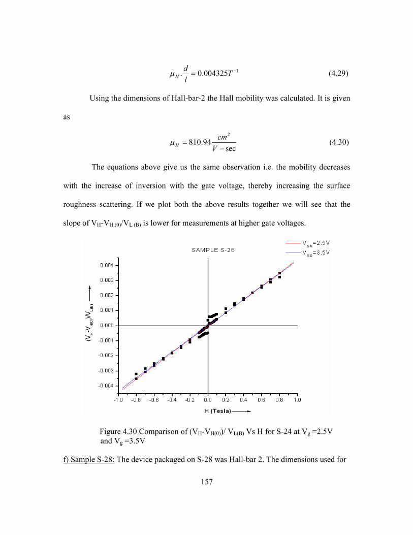
157
1004325.0. −= Tl
dHµ (4.29)
Using the dimensions of Hall-bar-2 the Hall mobility was calculated. It is given
as
sec
94.8102
−=
V
cmHµ (4.30)
The equations above give us the same observation i.e. the mobility decreases
with the increase of inversion with the gate voltage, thereby increasing the surface
roughness scattering. If we plot both the above results together we will see that the
slope of VH-VH (0)/VL (B) is lower for measurements at higher gate voltages.
Figure 4.30 Comparison of (VH-VH(0))/ VL(B) Vs H for S-24 at Vg =2.5V
and Vg =3.5V
f) Sample S-28: The device packaged on S-28 was Hall-bar 2. The dimensions used for

158
calculations are given in Fig. 4.31
Figure 4.31 Device under analysis on Sample S-28, Hall-Bar 2
The measurements on this sample were taken for a magnetic field range of 0.1
Tesla to 0.8 Tesla in both the magnetic field directions. The plot for Vgs= 0.75V is given
below in Fig. 4.32.
Figure 4.32 (VH-VH(0))/ VL(B) Vs H at Vg = 0.75 V for S-28

159
The slope of the linear fit gave us
1010991.0. −= Tl
dHµ (4.31)
Using the dimensions of Hall-bar-2 the Hall mobility was calculated.
sec
24.9342
−=
V
cmHµ (4.32)
Analysis was also done on this sample at Vgs=1.0V. The resultant graph is
shown below.
Figure 4.33 (VH-VH(0))/ VL(B) Vs H at Vg = 1.0V for S-28
The slope of the linear fit gave us

160
10099753.0. −= Tl
dHµ (4.33)
Using the dimensions of Hall-bar-2 the Hall mobility was calculated.
sec
90.8472
−=
V
cmHµ (4.34)
The equations above give us the same observation i.e. the mobility decreases
with the increase of inversion with the gate voltage, thereby increasing the surface
roughness scattering. If we plot both the above results together we will see that the
slope of VH-VH (0)/VL (B) is lower for measurements at higher gate voltages. This is
demonstrated with the following graph.
Figure 4.34 Comparison of (VH-VH(0))/ VL(B) Vs H for S-28 at Vg =0.75V
and Vg =1.0V

161
It was observed with the Hall mobility analysis that the Hall data follows a
particular trend with the magnetic field changes. The Hall data showed that the Hall
mobility is dependent upon scattering by surface roughness. Next, HfSiO samples will
be analyzed to find whether they agree with the data analysis done on the SiO2 samples,
i.e. whether the Hall data shows the same trend. But before that we can summarize the
results of Hall mobility calculations for SiO2 based samples as follows.
Table 4.2 Summary of Hall mobility results of SiO2 based samples
Sample Dimensions Range of
H
Vgs µH (cm2/V-s) Comments
0.5 V 1254.68 S-20
d = 40 µm
l = 340 µm
0.0 T to
0.7 T 0.75 V 1096.84
µH decreases with
increase in VGS
0.5 V 1742.65 S-21
d = 40 µm
l = 520 µm
0.0 T to
0.7 T 0.75 V 1387.49
µH decreases with
increase in VGS
0.5 V 2095.87 S-22 d = 40 µm
l = 750 µm
0.0 T to
0.8 T 0.75 V 1679.81
µH decreases with
increase in VGS
0.7 V 655.163 S-24 d = 40 µm
l = 340 µm
0.0 T to
0.8 T 0.8 V 621.73
µH decreases with
increase in VGS
2.5 V 827.25 S-26 d = 40 µm
l = 750 µm
0.0 T to
0.8 T 3.5 V 810.94
µH decreases with
increase in VGS
934.24 V S-28 d = 40 µm
l = 340 µm
0.0 T to
0.8 T
0.75 V
1.0 V 847.90 V
µH decreases with
increase in VGS
4.4.2 Samples with HfSiO as Gate Dielectric
The Hall mobility analysis was carried out on two High-k samples i.e. Sample
H-3 and Sample H-4. As the high-K transistors have higher threshold voltage, they were
tested on relatively higher gate voltages to have conduction.
a) Sample H-3: The device bonded and packaged on this sample was Hall-bar 2. The
measurements on this sample were taken under gate voltages 3.5V and 4.5V. The
dimensions are given in Fig. 4.35.

162
Figure 4.35 Device under analysis on Sample H-3, Hall-Bar 2
The measurements on this sample were taken for a magnetic field range of 0.1
Tesla to 0.8 Tesla in both the magnetic field directions. The same method was adopted
to calculate the Hall mobility as in the earlier samples with SiO2.The final plot for Vgs=
3.5V is shown in Fig. 4.36.
Figure 4.36 (VH-VH(0))/ VL(B) Vs H at Vg = 3.5V for H-3

163
The slope of the linear fit gave us
1006252.0. −= Tl
dHµ (4.35)
Using the dimensions of Hall-bar-2 the Hall mobility was calculated.
sec
42.5312
−=
V
cmHµ (4.36)
Result of the data with higher gate voltage of 4.5V is shown in Fig. 4.37. It is
interesting to note that the behavior of this HfSiO based sample is quite similar to the
SiO2 bases sample i.e. there is a decrease in Hall mobility with the increase in the gate
voltage. This will be demonstrated mathematically now.
Figure 4.37 (VH-VH(0))/ VL(B) Vs H at Vg = 4.5V for H-3
The slope of the linear fit gave us

164
10055498.0. −= Tl
dHµ (4.37)
Using the dimensions of Hall-bar-2 the Hall mobility was calculated.
sec
733.4712
−=
V
cmHµ (4.38)
This sample with HfSiO shows the trend in the reduction in Hall mobility with
the increase in the gate voltage as shown in the case of SiO2 samples. This can again be
attributed to surface roughness scattering. This statement is demonstrated in the graph
in Fig. 4.38.
Figure 4.38 Comparison of (VH-VH(0))/ VL(B) Vs H for H-3 at Vg =3.5V
and Vg =4.5V
b) Sample H-4: The device in this sample was Hall-bar 2. The dimensions are given as

165
in Fig. 4.39 below.
Figure 4.39 Device under analysis on Sample H-4, Hall-Bar 2.
The gate voltages under which this sample was analyzed were 1.40 V and 1.75
V. The magnetic field was swept from 0.0 Tesla to 0.8 Tesla and the measurements
were taken in both the magnetic field directions. The resultant graph of Vgs=1.40 V is
Figure 4.40 (VH-VH(0))/ VL(B) Vs H at Vg = 1.40V for H-4

166
The slope of the linear fit gave us
1006311.0. −= Tl
dHµ (4.39)
Using the dimensions of Hall-bar-2 the Hall mobility was calculated.
sec
44.5362
−=
V
cmHµ (4.40)
Looking into the analysis of sample H-4 with gate voltage Vgs=1.75V we
observe the following trend in the Hall data.
Figure 4.41 (VH-VH(0))/ VL(B) Vs H at Vg = 1.75V for H-4
The slope of the linear fit gave us
10060211.0. −= Tl
dHµ (4.41)
Using the dimensions of Hall-bar-2 the Hall mobility was calculated.

167
sec
78.5112
−=
V
cmHµ (4.42)
This sample H-4 shows the trend in the reduction in Hall mobility with the
increase in the gate voltage as shown in the case of SiO2 samples. This can again be
attributed to surface roughness scattering. This statement is demonstrated in the Fig.
4.42 below.
Figure 4.42 Comparison of (VH-VH(0))/ VL(B) Vs H for H-4 at Vg =1.4V
and Vg =1.75V
The Hall mobility results obtained thus far for HfSiO based samples can be
summarized as in Table 4.3.

168
Table 4.3 Summary of Hall mobility results of HfSiO based samples
Sample Dimensions Range of
H
Vgs µH (cm2/V-s) Comments
3.5 V 531.42 H-3
d = 40 µm
l = 340 µm
0.0 T to
0.8 T 4.5 V 471.73
µH decreases with
increase in VGS
1.40 V 536.44 H-4
d = 40 µm
l = 340 µm
0.0 T to
0.8 T 1.75 V 511.78
µH decreases with
increase in VGS
4.5 Comparison of Hall Mobility in SiO2 and HfSiO samples
Carrier mobility in the channel is the most challenging problem with the High-k
devices [76]. There are several factors that are responsible for the reduction in mobility
in the case of high-k transistors. Though SiO2 based transistors also suffer from the
mobility reduction, this is more pronounced in the case of high-k transistors [77]. In the
previous section the Hall mobility data on the SiO2 and HfSiO based Hall transistors
was analyzed. In this section we are going to compare the results obtained from the
previous section in accordance with the theory stated above.
We will look at two samples Sample S-28 and Sample H-4. Both these samples
had the same kind of device packaged i.e. Hall-bar 2 and the measurements taken were
almost on the same gate voltage data. The plots of Sample S-28 at VGS =1.0V and
Sample H-4 at VGS =1.40 Volts are shown in Fig. 4.43. These comparisons give us a
good insight about the mobilities of both Silicon Dioxide and High-K samples and also
about the mobility degradation in high-k dielectric based devices.

169
(a)
(b)
Figure 4.43 Comparison of µH(d/l) for (a) S-28 and (b) H-4

170
Sample S-28 = sec
90.8472
−=
V
cmHµ (4.43)
Sample H-4 = sec
44.5362
−=
V
cmHµ (4.44)
The above observations can be tabulated as follows.
Table 4.4 Comparison of Hall mobilities of S-28 and H-4
As it can be observed from the above two equations (4.43) and (4.44) and the
Table 4.3, though the various parameters like device dimensions and magnetic field
intensity were the same in both the measurements and the gate voltage was also almost
the same, it is observed that the Hall mobility in case of SiO2 sample S-28 is much
greater than the HfSiO sample H-4. Apart from the aforementioned samples, observing
and comparing other analyzed samples of SiO2 and HfSiO shows that the SiO2 based
samples have much higher mobility as compared to the HfSiO bases samples. This
shows that the phenomenon of mobility degradation is much more pronounced in the
case of high-k based devices as compared to the SiO2 based samples. As the magnetic
field under which these measurements are being taken range from 0.0 Tesla to 0.8
Tesla, this is considered to be low field regime. So along with the surface roughness
scattering, Coulomb scattering mechanisms can also be one of the factors responsible
Sample Dimensions Range of
H
Vgs µH (cm2/V-s)
0.75 V 934.24 V S-28 d = 40 µm
l = 340 µm
0.0 T to
0.8 T 1.0 V 847.90
1.40 V 536.44 H-4
d = 40 µm
l = 340 µm
0.0 T to
0.8 T 1.75 V 511.78

171
for the mobility degradation in high-k dielectrics due to the low field regime [48]. As
mentioned in section 3.4 there is an interfacial oxide between high-k layer and Silicon
surface. This interfacial oxide can also be a reason for the mobility degradation in high-
k transistors [48]. Also high-k materials have a large amount of fixed charges which can
lead to the reduction on the mobility as they can cause charge trapping resulting in
higher threshold voltage with diminishing mobility [37, 47]. But as the material used is
HfSiO, it has higher mobility degradation than other Hafnium based materials and this
material is capable of achieving mobilities almost equal to their SiO2 based counterparts
[48].

172
CHAPTER 5
CONCLUSION
5.1 Summary
This work was aimed at addressing one of the most critical issues in transistor
processing. Carrier mobility influences the device behavior to a large and important
extent. It plays a key role in characterizing the performance of a transistor. Carriers
suffer from mobility degradation in the channel due to various impeding mechanisms
like phonon scattering, Coulomb scattering, surface roughness scattering and the charge
trapping mechanisms. The charge traps like the fixed oxide charges, interface trapped
charges, mobile ionic charges and oxide trapped charges along with the charge
scattering mechanisms can influence the threshold voltage along with the carrier
mobility thereby affecting the transistor performance to a great extent.
Due to constant scaling of transistor dimensions in compliance with the Moore’s
law, the SiO2 based gate dielectric has already reached its physical limitations. As the
SiO2 thickness approaches to <1nm various problems like dielectric reliability and
quantum tunneling currents increase causing the dielectric leakage and subsequent
breakdown. This urged on researches to try different materials for gate dielectric with a
higher dielectric constant which could facilitate the use of a thicker gate layer thereby
reducing the leakage current problem but complying with the scaling demands of the
industry. Hafnium based materials hold the maximum promise due to their better

173
threshold voltage characteristics and better leakage characteristics as compared to other
high-k dielectric materials. But the high-k dielectric materials have some problems of
charge trapping and scattering, more enhanced than SiO2, which impede their smooth
adoption as gate dielectric in commercial devices. The various mechanisms contributing
to the mobility degradation in SiO2 based dielectrics and HfSiO based dielectric were
discussed in chapter 1. This work was motivated by the need to find out the difference
in mobility of the transistors with conventional dielectric SiO2 and Hafnium based
dielectric HfSiO and the need to find true drift mobility of carriers in the channel. Two
different mobility extraction techniques were discussed in Chapter 1- Hall Effect and
Split C-V measurements. As of time of writing of this thesis, extensive research goes on
in academic and industrial areas to find out the most stable replacement for SiO2. Intel
already claims to have started using alternate dielectric materials in its transistors.
MOSFETs with SiO2 and HfSiO were successfully fabricated. Chapter 2
discussed the process flow involved in the fabrication of the MOSFETs with both SiO2
and HfSiO. Along with the MOSFETs with different W/L ratios, other devices like
MOS Capacitors, Hall-bars, Carbino discs and Van Der Pauw devices were also
fabricated alongside the MOSFETs. The devices with both the dielectric materials were
fabricated using a process flow which was very similar except for some processing
steps like deposition of gate dielectric and etching of gate dielectric. SiO2 was grown
using dry thermal oxidation and etched using reactive ion etching procedure. Reactive
ion etch was used due to its anisotropic nature which avoids undercutting. HfSiO was

174
deposited using sputtering mechanism followed by annealing in argon and oxygen
environments and etched using buffered etch process.
The devices fabricated were characterized using different semiconductor
parameter analyzers. The I-V and C-V characterization was carried out on the
MOSFETs and MOS Capacitors respectively. Chapter 3 discussed the characterization
method and subsequent characteristics extracted from the fabricated devices. The I-V
characterization was performed to find out the validity of the fabricated MOSFET and
Hall-bars and find out the drain current under gate bias and drain to source bias. C-V
characterization was carried out on the MOS capacitors to extract various parameters
relating to the MOS system like insulator thickness, Debye length, flatband voltage etc.
These parameters were extracted using the Hauser program.
Split C-V measurements are sensitive to trapped charges. So this technique is
most suited for a system with less trapping like SiO2. But in case of higher trapping like
in high-k dielectric materials, this technique would not prove to be as successful. This
led us to another technique for mobility extraction. Hall Effect measurements are
insensitive to trapped charges so Hall measurements would not take trapped charges
into account giving mobility close to true mobility. Hall measurement technique and
results of Hall mobility extraction were described in chapter 4. It was concluded from
the measurement results that the Hall mobility is lower in HfSiO based transistors as
compared to the SiO2 based transistors. But despite of the fact that the high-k dielectric
based transistors suffer from mobility degradation, high-k dielectric materials like
HfSiO still seem to be the future of gate dielectric material in commercial transistors.

175
5.2 Future Work
More devices need to be fabricated with SiO2 and HfSiO as gate dielectric
materials. As described in chapter 3 the thickness of gate oxide is still in the 25nm-
40nm range. Devices with a thinner SiO2 need to be fabricated. We also hope to reduce
the thickness of the interfacial layer between silicon surface and HfSiO in our future
fabrication processes. This can be done by etching the wafer for a longer time in 2% HF
before the HfSiO deposition. At the same time we hope to go to a thinner HfSiO from
the present 20nm to 15nm range.
We need to do Hall mobility measurements on both SiO2 and HfSiO samples.
Though we have enough data for predicting the range of mobilities for SiO2 based
samples, we need more data on HfSiO bases samples to state the same about them.
The true motivation behind this project is to extract true carrier mobility both
incase of SiO2 based MOS devices and HfSiO based MOS devices. The work described
so far has been very exploratory in nature and the idea of extracting true mobility has
been nearly achieved. The achievements so far in this work have been significant as
they are the stepping stone to extracting the true channel drift mobility.
As described earlier, the true drift mobility is given as
HD r µµ .= (5.1)
where µD is the true drift mobility, r is the Hall factor and µH is the Hall mobility
[28, 59]. We have calculated the Hall mobility for the SiO2 based transistors and HfSiO
based transistors. The problem is that we have to know what the Hall factor is, to
calculate the true drift mobility from the Hall mobility. So the next stage is to calculate

176
the Hall factor. Since r depends on scattering mechanism, Fermi degeneracy, and
temperature, it will vary with gate voltage and from sample to sample. We propose that
we measure magnetoresistance, because theory indicates some correlation of r with it.
The Hall factor r is considered to be almost equal to 1 i.e. r~1. If r~1 is used in mobility
calculations, it can introduce error into measured mobility [28]. Like Hall Effect
magnetoresistance is also insensitive to trapped charges and is sensitive only to the
mobile charges. So if we can calculate the Hall factor r from magnetoresistance
calculations we can find out the true drift mobility.
Magnetoresistance is given as [28]
00
0
R
R
R
RRMR B ∆
=−
= (5.2)
where RB is the channel resistance in the presence of magnetic field, R0 is the
channel resistance in the absence of any magnetic field and ∆R is their difference. The
Hall factor r is given as [28]
22 / ⟩⟨⟩⟨= ττr (5.3)
where τ is the mean time between collisions for the carriers and <> indicates
average over all electron (or holes). The magnetoresistance is related to Hall mobility
by the following equation
( )24
00
0 10 HmR
R
R
RRMR H
B µ−=∆
=−
= (5.4)

177
where m is the magnetoresistance coefficient, µH is the Hall mobility and H is
the magnetic field intensity. The conjecture here is that the magnetoresistance
coefficient is related to the Hall factor.
The magnetoresistance coefficient is given as [28]
22223 /][ ⟩⟨⟩⟨−⟩⟩⟨⟨= ττττm (5.5)
And Hall factor r given in X can be modified as [28]
222 /][1 ⟩⟨⟩⟨−⟩⟨=− τττr (5.6)
The above two expressions look very similar which gives us an indication that
there can be a relation between the magnetoresistance coefficient m and Hall factor r.
By calculating the magnetoresistance coefficient we can calculate the Hall factor and
hence the true drift mobility. The magnetoresistance plot doesn’t pass through the origin
in the present scenario. This can be due to different reasons including the magnetic
package and other errors in measurement. The work is still being carried out extensively
on this subject.
In addition to find the drift mobility we also hope to increase the accuracy of the
Hall factor r with the help of magnetoresistance calculations. Hall factor r is considered
to be ~ 1 which can inject errors in the calculations. We hope to increase its accuracy.
The Carbino discs and Van Der Pauw devices also need to be analyzed. These devices
are specifically designed for magnetoresistance measurements. After the
magnetoresistance analysis on the Hall-bars we need to shift our focus on these devices
for magnetoresistance calculations. Low temperature measurements will be carried out
simultaneously to analyze the temperature dependence of carriers in the channel.

178
APPENDIX A
MASKS FOR FABRICATION

179
4-mask layer process for the fabrication of MOS devices was designed using L-
Edit. The die size was chosen so that each individual die could fit in the 16-pin DIP
package. The die spacing was chosen such that individual dies can be cleaved. The
minimum feature sizes in the devices were 10um for all mask layers. The alignment
mark is placed at the left top corner which has cross-wires of 4um width.
Die size: 4mm by 2.5mm
Mask type: Soda lime glass
Mask size: 5 inch by 5 inch
First Mask Layer- The first mask was used to open the diffusion areas on the
wafer. This was done to dope the p-type wafer with n-type dopant. Negative photoresist
was used for this purpose. This mask opened the areas like source and drain on the
wafer for doping. The fist mask layer is shown below.
Second Mask Layer: The second mask layer was used to etch away the field
oxide from the areas where the gate oxide could be grown or deposited. The second
mask is shown below.
Third Mask Layer: The third mask was used to pattern the areas for etching
the gate oxide. For example after the gate oxide was deposited, it had to be etched from
the source and drain regions. The third mask is shown in figure
Fourth Mask layer: The fourth mask was used to pattern the areas for metal
deposition. The fourth mask is shown below

180
Mask 1:
Mask 2

181
Mask 3:
Mask 4:

182
APPENDIX B
FABRICATION RECIPES

183
Three samples each were fabricated with SiO2 as gate dielectric and HfSiO as
gate dielectric. The fabrication recipes of each of these samples are being described in
this section in a tabulated form.
SI 001:
PROCESS PROCESS
SPECIFICATIONS
EQUIPMENT
USED
COMMENTS
Si wafer 2”,p-type, 1-10 Ω-cm,
<100>
Mask 1
Pre-clean RCA clean for 15 minutes Acid Hood
Field oxidation Wet Oxi.,1000oC, 1.75Hrs Oxid. Furnace Tox= 6000 A
PR coating HMDS- 4000 rpm, 60 sec
AZ2020-4000 rpm, 30 sec
Spinner PR
thickness=1.8µm
Pre-bake 110oC, 60 sec Hot plate
Exposure I-line lithography, 19.2sec Karl Suss I-line
aligner
Post Exposure
Bake
110oC, 60 sec Hot plate
Develop AZ 300MIF, 35 sec
Rinse with DI water
Solvent Hood
Wet Etch Field
Oxide
6:1 BHF, 6.5 min
Rinse with DI water
Acid Hood
PR stripping AZ 400T, 80oC, 15 mins
Rinse with DI water
Solvent Hood
Spin-on
Dopant
P5O8, 3000 rpm, 20 sec Spinner
Bake 200oC, 15 mins Oven
Drive-in Diff. 1100oC, 2.30 Hrs,
%N2:O2=75:25
Diffusion Furnace Xj= 2 µm
SOD Removal 10:1 HF 5.5 mins Acid Hood
Mask 2
PR coating HMDS- 4000 rpm, 60 sec
AZ2020-4000 rpm, 30 sec
Spinner PR
thickness=1.8µm
Pre-bake 110oC, 60 sec Hot plate
Exposure I-line lithography, 19.2sec Karl Suss I-line
aligner

184
Post Exposure
Bake
110oC, 60 sec Hot plate
Develop AZ 300MIF, 35 sec
Rinse with DI water
Solvent Hood
Wet Etch 6:1 BHF, 7 mins
Rinse with DI water
Acid Hood
PR stripping AZ 400T, 80oC, 15 mins
Rinse with DI water
Solvent Hood
Gate Oxide
Growth
Dry Oxidation, 70 psi O2,
1100oC, 30 mins
Oxidation furnace Xox= 33nm-36nm
Mask 3
PR coating HMDS- 4000 rpm, 60 sec
AZ2020-4000 rpm, 30 sec
Spinner PR
thickness=1.8µm
Pre-bake 110oC, 60 sec Hot plate
Exposure I-line lithography, 19.2sec Karl Suss I-line
aligner
Post Exposure
Bake
110oC, 60 sec Hot plate
Develop AZ 300MIF, 35 sec
Rinse with DI water
Solvent Hood
Dry etching 100W, CF4=30 sccm,
O2=0.9 sccm, 3.75 mins
Technics RIE
PR stripping AZ 400T, 80oC, 15 mins
Rinse with DI water
Solvent Hood
Mask 4
PR coating HMDS- 4000 rpm, 60 sec
AZ2020-4000 rpm, 30 sec
Spinner PR
thickness=1.8µm
Pre-bake 110oC, 60 sec Hot plate
Exposure I-line lithography, 19.2sec Karl Suss I-line
aligner
Post Exposure
Bake
110oC, 60 sec Hot plate
Develop AZ 300MIF, 35 sec
Rinse with DI water
Solvent Hood
Al deposition 10-6 Torr, 100 Amps NRC Thermal
Evaporator
Metal Thickness
=2000 A
Metal Lift-off AZ 400T, 80oC, 16 mins Solvent Hood

185
SI 002:
PROCESS PROCESS
SPECIFICATIONS
EQUIPMENT
USED
COMMENTS
Si wafer 4”,p-type, 1-10 Ω-cm,
<100>
Mask 1
Pre-clean RCA clean for 15 mins Acid Hood
Field oxidation Wet Oxi.,1100oC, 1.75Hrs Oxid. Furnace Tox= 6350 A
PR coating HMDS- 4000 rpm, 60 sec
AZ2020-4000 rpm, 30 sec
Spinner PR
thickness=1.8µm
Pre-bake 110oC, 60 sec Hot plate
Exposure I-line lithography, 5.5.sec OAI backside
aligner
Post Exposure
Bake
110oC, 60 sec Hot plate
Develop AZ 300MIF, 35 sec
Rinse with DI water
Solvent Hood
Wet Etch Field
Oxide
6:1 BHF, 7.25 mins
Rinse with DI water
Acid Hood
PR stripping AZ 400T, 80oC, 15 mins
Rinse with DI water
Solvent Hood
Spin-on
Dopant
P5O8, 3000 rpm, 20 sec Spinner
Bake 200oC, 15 mins Oven
Drive-in Diff. 1100oC, 3.0 Hrs,
%N2:O2=75:30
Diffusion Furnace Xj= 2 µm
SOD Removal 10:1 HF 6 mins Acid Hood
Mask 2
PR coating HMDS- 4000 rpm, 60 sec
AZ2020-4000 rpm, 30 sec
Spinner PR
thickness=1.8µm
Pre-bake 110oC, 60 sec Hot plate
Exposure I-line lithography, 5.5.sec OAI backside
aligner
Post Exposure
Bake
110oC, 60 sec Hot plate
Develop AZ 300MIF, 35 sec
Rinse with DI water
Solvent Hood
Wet Etch 6:1 BHF, 6.5 mins
Rinse with DI water
Acid Hood

186
PR stripping AZ 400T, 80oC, 15 mins
Rinse with DI water
Solvent Hood
Gate Oxide
Growth
Dry Oxidation, 70 psi O2,
1100oC, 30 mins
Oxidation furnace Xox= 24nm-27nm
Mask 3
PR coating HMDS- 4000 rpm, 60 sec
AZ2020-4000 rpm, 30 sec
Spinner PR
thickness=1.8µm
Pre-bake 110oC, 60 sec Hot plate
Exposure I-line lithography, 5.5.sec OAI backside
aligner
Post Exposure
Bake
110oC, 60 sec Hot plate
Develop AZ 300MIF, 35 sec
Rinse with DI water
Solvent Hood
Dry etching 100W, CF4=30 sccm,
O2=0.9 sccm, 2.5 mins
Technics RIE
PR stripping AZ 400T, 80oC, 15 mins
Rinse with DI water
Solvent Hood
Mask 4
PR coating HMDS- 4000 rpm, 60 sec
AZ2020-4000 rpm, 30 sec
Spinner PR
thickness=1.8µm
Pre-bake 110oC, 60 sec Hot plate
Exposure I-line lithography, 5.5.sec OAI backside
aligner
Post Exposure
Bake
110oC, 60 sec Hot plate
Develop AZ 300MIF, 35 sec
Rinse with DI water
Solvent Hood
Al deposition 10-6 Torr, 100 Amps NRC Thermal
Evaporator
Metal Thickness
=2000 A
Metal Lift-off AZ 400T, 80oC, 35 mins Solvent Hood
SI 003:
PROCESS PROCESS
SPECIFICATIONS
EQUIPMENT
USED
COMMENTS
Si wafer 4”,p-type, 1-10 Ω-cm,
<100>
Mask 1
Pre-clean RCA clean for 15 mins Acid Hood

187
Field oxidation Wet Oxi.,1100oC, 1.5Hrs Oxid. Furnace Tox= 5600 A
PR coating HMDS- 4000 rpm, 60 sec
AZ2020-4000 rpm, 30 sec
Spinner PR
thickness=1.8µm
Pre-bake 110oC, 60 sec Hot plate
Exposure I-line lithography, 5.5.sec OAI backside
aligner
Post Exposure
Bake
110oC, 60 sec Hot plate
Develop AZ 300MIF, 35 sec
Rinse with DI water
Solvent Hood
Wet Etch Field
Oxide
6:1 BHF, 7 mins
Rinse with DI water
Acid Hood
PR stripping AZ 400T, 70oC, 15 mins
Rinse with DI water
Solvent Hood
Spin-on
Dopant
P5O8, 3000 rpm, 20 sec Spinner
Bake 200oC, 15 mins Oven
Drive-in Diff. 1100oC, 3 Hrs,
%N2:O2=80:30
Diffusion Furnace Xj= 2 µm
SOD Removal 10:1 HF 5.10 mins Acid Hood
Mask 2
PR coating HMDS- 4000 rpm, 60 sec
AZ2020-4000 rpm, 30 sec
Spinner PR
thickness=1.8µm
Pre-bake 110oC, 60 sec Hot plate
Exposure I-line lithography, 5.5.sec OAI backside
aligner
Post Exposure
Bake
110oC, 60 sec Hot plate
Develop AZ 300MIF, 35 sec
Rinse with DI water
Solvent Hood
Wet Etch 6:1 BHF, 4.5 mins
Rinse with DI water
Acid Hood
PR stripping AZ 400T, 80oC, 15 mins
Rinse with DI water
Solvent Hood
Gate Oxide
Growth
Dry Oxidation, 70 psi O2,
1100oC, 35 mins
Oxidation furnace Xox= 35nm
Mask 3
PR coating HMDS- 4000 rpm, 60 sec
AZ2020-4000 rpm, 30 sec
Spinner PR
thickness=1.8µm
Pre-bake 110oC, 60 sec Hot plate

188
Exposure I-line lithography, 5.5.sec OAI backside
aligner
Post Exposure
Bake
110oC, 60 sec Hot plate
Develop AZ 300MIF, 35 sec
Rinse with DI water
Solvent Hood
Dry etching 100W, CF4=30 sccm,
O2=0.9 sccm, 3.5 mins
Technics RIE
PR stripping AZ 400T, 80oC, 15 mins
Rinse with DI water
Solvent Hood
Mask 4
PR coating HMDS- 4000 rpm, 60 sec
AZ2020-4000 rpm, 30 sec
Spinner PR
thickness=1.8µm
Pre-bake 110oC, 60 sec Hot plate
Exposure I-line lithography, 5.5.sec OAI backside
aligner
Post Exposure
Bake
110oC, 60 sec Hot plate
Develop AZ 300MIF, 35 sec
Rinse with DI water
Solvent Hood
Al deposition 10-6 Torr, 100 Amps NRC Thermal
Evaporator
Metal Thickness
=1500 A
Metal Lift-off AZ 400T, 80oC, 15 mins Solvent Hood
HK 008:
PROCESS PROCESS
SPECIFICATIONS
EQUIPMENT
USED
COMMENTS
Si wafer 4”,p-type, 1-10 Ω-cm,
<100>
Mask 1
Pre-clean RCA clean for 15 mins Acid Hood
Field oxidation Wet Oxi.,1100oC, 2.05Hrs Oxid. Furnace Tox= 6900 A
PR coating HMDS- 4000 rpm, 60 sec
AZ2020-4000 rpm, 30 sec
Spinner PR
thickness=1.8µm
Pre-bake 110oC, 60 sec Hot plate
Exposure I-line lithography, 5.5.sec OAI backside
aligner
Post Exposure
Bake
110oC, 60 sec Hot plate

189
Develop AZ 300MIF, 35 sec
Rinse with DI water
Solvent Hood
Wet Etch Field
Oxide
6:1 BHF, 11 mins
Rinse with DI water
Acid Hood
PR stripping AZ 400T, 70oC, 15 mins
Rinse with DI water
Solvent Hood
Spin-on
Dopant
P5O8, 3000 rpm, 20 sec Spinner
Bake 200oC, 15 mins Oven
Drive-in Diff. 1100oC, 3.0 Hrs,
%N2:O2=77:28
Diffusion Furnace Xj= 2 µm
SOD Removal 10:1 HF 5.5 mins Acid Hood
Mask 2
PR coating HMDS- 4000 rpm, 60 sec
AZ2020-4000 rpm, 30 sec
Spinner PR
thickness=1.8µm
Pre-bake 110oC, 60 sec Hot plate
Exposure I-line lithography, 5.5.sec OAI backside
aligner
Post Exposure
Bake
110oC, 60 sec Hot plate
Develop AZ 300MIF, 35 sec
Rinse with DI water
Solvent Hood
Wet Etch 6:1 BHF, 8 mins
Rinse with DI water
Acid Hood
PR stripping AZ 400T, 80oC, 15 mins
Rinse with DI water
Solvent Hood
Pre Deposition
Etch
2% HF, 30 sec Acid Hood
Gate Oxide
Growth
Sputtering of HfSi2
target,1min, 50 Watts
Xox= 20nm
UV Oxidation UV Ozone oxidation, 30
min
Anneal Ar-350oC, 0.5 Hrs
O2-350oC, 0.5 Hrs
Mask 3
PR coating HMDS- 4000 rpm, 60 sec
AZ2020-4000 rpm, 30 sec
Spinner PR
thickness=1.8µm
Pre-bake 110oC, 60 sec Hot plate
Exposure I-line lithography, 5.5.sec OAI backside
aligner
Post Exposure 110oC, 60 sec Hot plate

190
Bake
Develop AZ 300MIF, 35 sec
Rinse with DI water
Solvent Hood
Wet etching 2% HF, 1.10 mins Acid Hood
PR stripping AZ 400T, 80oC, 15 mins
Rinse with DI water
Solvent Hood
Mask 4
PR coating HMDS- 4000 rpm, 60 sec
AZ2020-4000 rpm, 30 sec
Spinner PR
thickness=1.8µm
Pre-bake 110oC, 60 sec Hot plate
Exposure I-line lithography, 5.5.sec OAI backside
aligner
Post Exposure
Bake
110oC, 60 sec Hot plate
Develop AZ 300MIF, 35 sec
Rinse with DI water
Solvent Hood
Al deposition 10-6 Torr, 100 Amps NRC Thermal
Evaporator
Metal Thickness
=1800 A
Metal Lift-off AZ 400T, 80oC, 15 mins Solvent Hood
HK 009:
PROCESS PROCESS
SPECIFICATIONS
EQUIPMENT
USED
COMMENTS
Si wafer 4”,p-type, 1-10 Ω-cm,
<100>
Mask 1
Pre-clean RCA clean for 15 mins Acid Hood
Field oxidation Wet Oxi.,1100oC, 2.10Hrs Oxid. Furnace Tox= 6200 A
PR coating HMDS- 4000 rpm, 60 sec
AZ2020-4000 rpm, 30 sec
Spinner PR
thickness=1.8µm
Pre-bake 110oC, 60 sec Hot plate
Exposure I-line lithography, 5.5.sec OAI backside
aligner
Post Exposure
Bake
110oC, 60 sec Hot plate
Develop AZ 300MIF, 35 sec
Rinse with DI water
Solvent Hood

191
Wet Etch Field
Oxide
6:1 BHF, 10 mins
Rinse with DI water
Acid Hood
PR stripping AZ 400T, 70oC, 15 mins
Rinse with DI water
Solvent Hood
Spin-on
Dopant
P5O8, 3000 rpm, 20 sec Spinner
Bake 200oC, 15 mins Oven
Drive-in Diff. 1100oC, 3.0 Hrs,
%N2:O2=80:35
Diffusion Furnace Xj= 2 µm
SOD Removal 10:1 HF 6.5 mins Acid Hood
Mask 2
PR coating HMDS- 4000 rpm, 60 sec
AZ2020-4000 rpm, 30 sec
Spinner PR
thickness=1.8µm
Pre-bake 110oC, 60 sec Hot plate
Exposure I-line lithography, 5.5.sec OAI backside
aligner
Post Exposure
Bake
110oC, 60 sec Hot plate
Develop AZ 300MIF, 35 sec
Rinse with DI water
Solvent Hood
Wet Etch 6:1 BHF, 9 mins
Rinse with DI water
Acid Hood
PR stripping AZ 400T, 80oC, 15 mins
Rinse with DI water
Solvent Hood
Pre Deposition
Etch
2% HF, 30 sec Acid Hood
Gate Oxide
Growth
Sputtering of HfSi2
target,1min, 50 Watts
Xox= 20nm
UV Oxidation UV Ozone oxidation, 30
min
Anneal Ar-350oC, 0.5 Hrs
O2-350oC, 0.5 Hrs
Mask 3
PR coating HMDS- 4000 rpm, 60 sec
AZ2020-4000 rpm, 30 sec
Spinner PR
thickness=1.8µm
Pre-bake 110oC, 60 sec Hot plate
Exposure I-line lithography, 5.5.sec OAI backside
aligner
Post Exposure
Bake
110oC, 60 sec Hot plate
Develop AZ 300MIF, 35 sec Solvent Hood

192
Rinse with DI water
Wet etching 2% HF, 1.0 mins Acid Hood
PR stripping AZ 400T, 80oC, 15 mins
Rinse with DI water
Solvent Hood
Mask 4
PR coating HMDS- 4000 rpm, 60 sec
AZ2020-4000 rpm, 30 sec
Spinner PR
thickness=1.8µm
Pre-bake 110oC, 60 sec Hot plate
Exposure I-line lithography, 5.5.sec OAI backside
aligner
Post Exposure
Bake
110oC, 60 sec Hot plate
Develop AZ 300MIF, 35 sec
Rinse with DI water
Solvent Hood
Al deposition 10-6 Torr, 100 Amps NRC Thermal
Evaporator
Metal Thickness
=2000 A
Metal Lift-off AZ 400T, 80oC, 15 mins Solvent Hood
HK 010:
PROCESS PROCESS
SPECIFICATIONS
EQUIPMENT
USED
COMMENTS
Si wafer 4”,p-type, 1-10 Ω-cm,
<100>
Mask 1
Pre-clean RCA clean for 15 mins Acid Hood
Field oxidation Wet Oxi.,1100oC, 2.05Hrs Oxid. Furnace Tox= 6800 A
PR coating HMDS- 4000 rpm, 60 sec
AZ2020-4000 rpm, 30 sec
Spinner PR
thickness=1.8µm
Pre-bake 110oC, 60 sec Hot plate
Exposure I-line lithography, 5.5.sec OAI backside
aligner
Post Exposure
Bake
110oC, 60 sec Hot plate
Develop AZ 300MIF, 35 sec
Rinse with DI water
Solvent Hood
Wet Etch Field
Oxide
6:1 BHF, 11 mins
Rinse with DI water
Acid Hood
PR stripping AZ 400T, 70oC, 15 mins Solvent Hood

193
Rinse with DI water
Spin-on
Dopant
P5O8, 3000 rpm, 20 sec Spinner
Bake 200oC, 15 mins Oven
Drive-in Diff. 1100oC, 3 Hrs,
%N2:O2=77:28
Diffusion Furnace Xj= 2 µm
SOD Removal 10:1 HF 5.5 mins Acid Hood
Mask 2
PR coating HMDS- 4000 rpm, 60 sec
AZ2020-4000 rpm, 30 sec
Spinner PR
thickness=1.8µm
Pre-bake 110oC, 60 sec Hot plate
Exposure I-line lithography, 5.5.sec OAI backside
aligner
Post Exposure
Bake
110oC, 60 sec Hot plate
Develop AZ 300MIF, 35 sec
Rinse with DI water
Solvent Hood
Wet Etch 6:1 BHF, 10 mins
Rinse with DI water
Acid Hood
PR stripping AZ 400T, 80oC, 15 mins
Rinse with DI water
Solvent Hood
Pre Deposition
Etch
2% HF, 30 sec Acid Hood
Gate Oxide
Growth
Sputtering of HfSi2
target,1min, 50 Watts
Xox= 20nm
UV Oxidation UV Ozone oxidation, 30
min
Anneal Ar-350oC, 0.5 Hrs
O2-350oC, 0.5 Hrs
Mask 3
PR coating HMDS- 4000 rpm, 60 sec
AZ2020-4000 rpm, 30 sec
Spinner PR
thickness=1.8µm
Pre-bake 110oC, 60 sec Hot plate
Exposure I-line lithography, 5.5.sec OAI backside
aligner
Post Exposure
Bake
110oC, 60 sec Hot plate
Develop AZ 300MIF, 35 sec
Rinse with DI water
Solvent Hood
Wet etching 2% HF, 55 sec Acid Hood

194
PR stripping AZ 400T, 80oC, 15.0 mins
Rinse with DI water
Solvent Hood
Mask 4
PR coating HMDS- 4000 rpm, 60 sec
AZ2020-4000 rpm, 30 sec
Spinner PR
thickness=1.8µm
Pre-bake 110oC, 60 sec Hot plate
Exposure I-line lithography, 5.5.sec OAI backside
aligner
Post Exposure
Bake
110oC, 60 sec Hot plate
Develop AZ 300MIF, 35 sec
Rinse with DI water
Solvent Hood
Al deposition 10-6 Torr, 100 Amps NRC Thermal
Evaporator
Metal Thickness
=2000 A
Metal Lift-off AZ 400T, 80oC, 25 mins Solvent Hood
195
REFERENCES
[1] G. E. Moore, “Cramming More Components onto Integrated Circuits”, Proceedings
of the IEEE, Vol. 86, No. 1, January 1998, pp. 82-85.
[2] P.A Packan, “Device Physics: Pushing the Limits”, Science 24, Vol. 285, No. 5436,
September 1999, pp. 2079-2081.
[3] G. E. Moore, “No Exponential is Forever: But “Forever” can be Delayed”, IEEE
International Solid-State Circuits Conference, ISSCC 2003/Session 1, 2003.
[4] H.-S. P. Wong, “Beyond the conventional transistor”, IBM J. Res. & Dev., Vol. 46,
No. 2/3, March/May 2002, pp. 133-168.
[5] The National Technology Roadmap for Semiconductors, 3rd edition, Semiconductor
Industry Association, San Jose, CA, 1997.
[6] Chris A. Mack, “Trends in Optical Lithography”, Optics and Photonics News, April
1996, pp. 29-33
[7] D. A. Buchanan, “Scaling the gate dielectric: Materials, integration and reliability”,
IBM J. Res. Develop., Vol. 43, No. 3, May 1999, pp. 245-264.
[8] S.-M. Kang, Y. Leblebici, “CMOS Digital Integrated Circuits”, Tata-McGraw-Hill,
New Delhi, 2003.
[9] R. S. Muller, T. I. Kamins, M. Chan, “Device Electronics for Integrated Circuits”,
John Wiley & Sons, 2003.
[10] http://www.mtmi.vu.lt/pfk/funkc_dariniai/transistor/mosfet.htm

196
[11] http://people.deas.harvard.edu/~jones/es154/lectures/lecture_3/darmstadt/sld002
.htm.
[12] J. Batista, A. Mandelis, D. Shaughnessy, “Temperature dependence of carrier
mobility in Si wafers measured by infrared photocarrier radiometry”, Applied Physics
Letters, Vol. 82, No. 23, 9 June 2003, pp. 4077-4079.
[13] http://ece-www.colorado.edu/~bart/book/book/chapter2/ch2_7.htm#2_7_1
[14] H. C. Casey, Jr., “Devices for Integrated Circuits, Si and III-V compound
semiconductors”, John Wiley & Sons, 1999.
[15] S.-I. Takagi, A. Toriumi, M. Iwase, H. Tango, “On the Universality of Inversion
Layer Mobility in Si MOSFET’s: Part I- Effects of Substrate Impurity Concentration”,
IEEE Transactions on Electron Devices, Vol. 41, No. 12, December 1994, pp. 2357-
2362.
[16] J. R. Hauser, “Extraction of Experimental Mobility Data for MOS Devices”, IEEE
Transactions on Electron Devices, Vol. 43, No. 11, November 1996, pp. 1981-1988.
[17] S.-I. Takagi, A. Toriumi, M. Iwase, H. Tango, “On the Universality of Inversion
Layer Mobility in Si MOSFET’s: Part II- Effects of Surface Orientation”, IEEE
Transactions on Electron Devices, Vol. 41, No. 12, December 1994, pp. 2363-2368.
[18] S.-I. Takagi, M. Takayanagi, “Experimental Evidence of Inversion Layer Mobility
Lowering in Ultrathin Gate Oxide Metal-Oxide-Semiconductor Field-Effect-Transistors
with Direct Tunneling Current”, Jpn. J. Appl. Phys., Vol. 41, April 2002, pp. 2348-
2352.

197
[19] S. C. Sun, J. D. Plummer, “Electron Mobility in Inversion and Accumulation
Layers on Thermally Oxidized Silicon Surfaces”, IEEE Journal of Solid State Circuits,
Vol. SC-15, No. 4, August 1980, pp. 562-573.
[20] Y. C. Cheng, E. A. Sullivan, “On the Role of Scattering by Surface Roughness in
Silicon Inversion Layers”, J. Appl. Phys., Vol. 45, No. 1, 1974, pp. 717-731.
[21] F. Gamiz, M. V. Fischetti, “Remote Coulomb scattering in metal-oxide-
semiconductor field effect transistors: Screening by electrons in the gate”, Applied
Physics Letters, Vol. 83, No. 23, 8 December 2003, pp. 4848-4850.
[22] G. Formicone, M. Saraniti, D. Z. Vasileska, D. K. Ferry, “ Study of a 50-nm
nMOSFET by Ensemble Monte Carlo Simulation Including a New Approach to Surface
Roughness and Impurity Scattering in the Si Inversion Layer”, IEEE Transactions on
Electron Devices, Vol. 49, No. 1, January 2002, pp. 125-132.
[23] G. Mazzoni, A. L. Lacaita, L. M. Perron, A. Pirovano, “On Surface Roughness-
Limited Mobility in Highly Doped n-MOSFET’s”, IEEE Transactions on Electron
Devices, Vol. 46, No. 7, July 1999, pp. 1423-1428.
[24] F. Fang, S. Triebwasser, “Effect of surface scattering on electron mobility in an
inversion layer on p-type silicon”, Applied Physics Letters, Vol. 4, No. 8, 15 April
1964, pp. 145-147.
[25] E. H. Nicollian, J. R. Brews, “MOS (Metal Oxide Semiconductor) Physics and
Technology”, John Wiley & Sons, 1982.

198
[26] M.-S. Liang, C. Chang, Y. T. Yeow, C. Hu, R. W. Brodersen, “MOSFET
degradation due to stressing of thin oxide”, IEEE Transactions on Electron Devices,
Vol. ED-31, No. 9, September1984, pp. 1238-11244.
[27] R. R. Razouk, B. E. Deal, “Dependence of Interface Trap Density on Silicon
Thermal Oxidation Process Variables”, J. Electrochem. Soc., Vol. 126, September
1979, pp. 1573-1581.
[28] D. K. Schroder, “Semiconductor material and device characterization”, John Wiley
& Sons, 1990.
[29] R. Chau, “Advance Metal Gate/High-K Dielectric Stacks for High-Performance
CMOS Transistors”, ICMI 2004.
[30] G.D Wilk, R. M. Wallace, J. M. Anthony, “High-K dielectrics: Current status and
materials properties considerations”, Journal of Applied Physics, Vol. 89, No. 10, 15
May 2001, pp. 5243-5275.
[31] M. Houssa, “High-K Gate Dielectrics”, IOP Publishing Ltd., 2004.
[32] G. Bersuker, B. H. Lee, H. R. Huff, “Novel Dielectric Materials for Future
Transistor Generations”, Proceedings of 2004 Workshop on Frontiers in Electronics.
[33] G. Groeseneken, L. Pantisano, L. A. Ragnarsson, R. Degraeve, M. Houssa, T.
Kauerauf, P. Roussel, S. D. Gendt, M. Heyns, “Achievements and Challenges for the
Electrical Performance of MOSFET’s with High-K Dielectrics”, Proceedings of 11th
IPFA 2004, Taiwan.
[34] T. P. Ma. “High-K Gate Dielectrics for Scaled CMOS Technology”, IEEE, 2001,
pp. 297-302.

199
[35] T.-J. King, H. Takeuchi, W.-C. Lee, Pushkar Ranade, “Novel Materials and
Processes for MOS Devices”, Final Report for MICRO Project 98-071, 1998-1999.
[36] J. C. Lee, “Hf-based High-K Dielectrics”, IWGI 2003, Tokyo, pp. 4-9.
[37] A. S. Oates, “Reliability Issues for High-K Gate Dielectrics”, IEDM 03, IEEE,
2003, pp. 923-926.
[38] M. A. Q. Lopez, M. El-Bouanani, B. E. Gnade, R. M. Wallace, M. R. Visokay, M.
Douglas, M. J. Bevan, L. Colombo, “Interdiffusion studies for HfSixOy and ZrSixOy on
Si”, Journal of Applied Physics, Vol.92, No. 7, 1 October 2002, pp. 3540-3550.
[39] P. Punchaipetch, G. Pant, M. A. Q. Lopez, C. Yao, M. El-Bouanani, M. J. Kim, R.
M. Wallace, B. E. Gnade, “Low Temperature Deposition of Hafnium Silicate Gate
Dielectrics”, IEEE Journal of Selected Topics in Quantum Electronics, Vol. 10, No. 1,
January/February 2004, pp. 89-100.
[40] M. A. Q. Lopez, M. El-Bouanani, B. E. Gnade, R. M. Wallace, “Wet chemical
etching studies of Zr and Hf silicate gate dielectrics”, J. Vac. Sci. Technol., A 20(6),
Nov/Dec 2002, pp. 1891-1897.
[41] Y. Xuan, T. Yasuda, “Vapor-Liquid Hybrid Deposition (VALID) of Hafnium
Silicate Films using Hf(OC4H9)4 and Si(OC2H5)4 Precursors”, IWGI 2003, Tokyo, pp.
24-27.
[42] J. Robertson, “Band offsets of wide band gap oxides and implications for future
electronic devices”, J. Vac. Sci. Technol., B 18(3), May/Jun 2000, pp. 1785-1791.

200
[43] M. Houssa, M. Naili, V. V. Afanas’ev, M. M. Heyns, A. Stesmans, “Electrical and
Physical Characterization of High-K Dielectric Layers”, IEEE, 2001.
[44] J. Chen, W. J. Yoo, Z. Y. Tan, Y. Wang, D. S. H. Chan, “Investigation of etching
properties of HfO based High-K dielectrics using inductively coupled plasma”, J. Vac.
Sci. Technol., A 22(4), Jul/Aug 2004, pp. 1552-1558.
[45] G. D. Wilk, R. M. Wallace, J. M. Anthony, “Hafnium and zirconium silicates for
advanced gate dielectrics”, Journal of Applied Physics, Vol. 87, No. 1, 1 January 2000,
pp. 484-492.
[46] A. Callegari, E. Cartier, M. Gribelyuk, H.F. O. Schmidt, T. Zabel, “Physical and
electrical characterization of Hafnium oxide and Hafnium silicate sputtered films”,
Journal of Applied Physics, Vol. 90, No. 12, 15 December 2001, pp. 6466-6475.
[47] P. Srinivasan, N. A. Chowdhury, D. Misra, “Charge Trapping in Ultrathin Hafnium
Silicate/Metal Gate Stacks”, IEEE Electron Device Letters, Vol. 26, No. 12, December
2005, pp. 913-915.
[48] Z. Ren, M. V. Fischetti, E. P. Gusev, E. A. Cartier, M. Chudzik, “Invesion channel
mobility in high-k high performance MOSFETs”, IBM SRDC, IEDM 03, IEEE 2003,
pp. 793-796.
[49] R. Chau, S. Datta, M. Doczy, J. Kavalieros, M. Metz, “Gate Dielectric Scaling for
High-Performance CMOS: from SiO2 to High-K”, IWGI, 2003, Tokyo.
[50] G. S. Lujan, S. Kubicek, S. De Gendt, M. Heyns, W. Magnus, K. De Meyer,
“Mobility Degradation in High-K Transistors: The Role of Charge Scattering”, IEEE,
2003.

201
[51] W. J. Zhu, T. P. Ma, “Temperature Dependence of Channel Mobility in HfO2
Gated NMOSFETs”, IEEE Electron Device Letters, Vol. 25, No. 2, February 2004, pp.
89-91.
[52] W. J. Zhu, J.-P Han, T. P. Ma, “Mobility Measurement and Degradation
Mechanisms of MOSFETs Made With Ultrathin High-k Dielectrics”, IEEE
Transactions on Electron Devices, Vol. 51, No. 1, January 2004, pp. 98-105.
[53] R. Chau, S. Datta, M. Doczy, B. Doyle, J. Kavalieros, M. Metz, “High-k/Metal
Gate Stack and Its MOSFET Characteristics”, IEEE Electron Device Letters, Vol. 25,
No. 6, June 2004, pp. 408-410.
[54] J. Chen, R. Carter, E. Cartier, M. Caymax, M. Claes, T. Conard, A, Delabie, W.
Deweerd, V. Kaushik, A. Kerber, S. Kubicek, J. W. Maes, M. Niwa, L. Pantisano, R.
Puurunen, L. Ragnarsson, T. Schram, Y. Shimamoto, W. Tsai, E. Rohr, S. V. Elshocht,
T. Witters, E. Young, C. Zhao, M. Heyns, “Implementation of high-k gate dielectrics-a
status update”, IWGI 2003, Tokyo.
[55] M. V. Fischetti, D. A Neumayer, E. A. Cartier, “Effective electron mobility in Si
inversion layers in metal-oxide-semiconductor systems with a high-k insulator: the role
of remote phonon scattering”, Journal of Applied Physics, Vol. 90, No. 9, 1 November
2001, pp. 4587-4608.
[56] J. A. Felix, M. R. Shaneyfelt, D. M. Fleetwood, J. R. Schwank, P. E. Dodd, E. P.
Gusev, R. M. Fleming, C. D’Emic, “Charge Trapping and Annealing in High-k Gate
Dielectrics”, IEEE Transactions of Nuclear Science, Vol. 51, No. 6, December 2004.
[57] ece-www.colorado.edu/~bart/book/book/chapter2/pdf/ch2_7_5.pdf

202
[58] S. Kasap, “Hall Effect in Semiconductors”, caltech.edu courses, an e-Booklet, S.
O. Kasap, 1990-2001.
[59] C. Kittel, “Introduction to Solid State Physics”, John Wiley & Sons, 2004.
[60] C. –L. Huang, G. S. Gildenblat, “Correction Factor in the Split C-V method for
Mobility Measurements”, Solid State Electronics, Vol. 36, No. 4, 1993, pp. 611-615.
[61] C. –L. Huang, J. V. Faricelli, Narain D. Arora, “A New Technique for Measuring
MOSFET Inversion Layer Mobility”, IEEE Transactions of Electron Devices, Vol. 40,
No. 6, June 1993, pp. 1134-1139.
[62] J. Koomen, “Investigation of the Most Channel Conductance in Weak Inversion”,
Solid State Electronics, vol. 16, 1973, pp. 801-810.
[63] F. Lime, C. Guiducci, R. Clerc, G. Ghibaudo, C. Leroux, T. Ernst,
“Characterization of effective mobility by split (CV) technique in N-MOSFETs with
ultra-thin gate oxides”, Solid State Electronics, 47, 2003, pp. 1147-1153.
[64] S. Wolf, R. N. Tauber, “Silicon Processing for the VLSI Era”, Lattice Press, 2nd
Edition, 2000.
[65] K. Pelhos, V. M. Donnelly,A. Kornblit, M. L. Green, R. B. Van Dover, L.
Manchanda, Y. Hu, M. Morris, E. Bower, “Etching of high-k dielectric Zr1-xAlxOy films
in chlorine-containing plasmas”, J. Vac. Sci. Technol. A 19(4), Jul/Aug 2001, pp. 1361-
1366.
[66] L. Sha and J. P. Changa, “Plasma etching of high dielectric constant materials on
silicon in halogen chemistries”, J. Vac. Sci. Technol. A 22(1), Jan/Feb 2004, pp. 88-95.

203
[67] L. Sha, R. Puthenkovilakam, Y. S. Lin, J. P Chang, “Ion-enhanced chemical
etching of HfO2 for integration in metal-oxide-semiconductor field effect transistors”, J.
Vac. Sci. Technol. B 21(6), Nov/Dec 2003, pp. 2420-2427.
[68] M. Helot, T. Chevolleau, L. Vallier, O. Joubert, E. Blanquet, A. Pisch, P.
Mangiagalli, T. Lill, “Plasma etching of HfO2 at elevated temperatures in chlorine
based chemistry”, J. Vac. Sci. Technol. A 24(1), Jan/Feb 2006, pp. 30-40.
[69] K. Christenson, “Selective wet etching of high-k materials”, FSI International,
Chaska, Minnisota.
[70] C.-H. Choi, Y. Wu, J.-S. Goo, Z. Yu, R. W. Dutton, “Capacitance Reconstruction
from Measured C-V in high-Leakage, Nitride/Oxide MOS”, IEEE Transactions on
Electron Devices, Vol. 47, No. 10, October 2000, pp. 1843-1850.
[71] A. Nara, N. Yasuda, H. Satake, A. Toriumi, “Applicability Limits of the Two-
Frequency Capacitance Measurement Technique for the Thickness Extraction of
Ultrathin Gate Oxide”, IEEE Transactions on Semiconductor Manufacturing, Vol. 15,
No. 2, May 2002, pp.209-213.
[72] K. J. Yang, C. Hu, “MOS Capacitance Measurements for High-Leakage Thin
Dielectrics”, IEEE Transactions on Electronic Devices, Vol. 46, No. 7, July 1999, pp.
1500-1501.

204
BIOGRAPHICAL INFORMATION
Rakshit Agrawal was born on September 4, 1981 in Bareilly, Uttar Pradesh,
India. He completed his Bachelor of Engineering (B.E.) from Priyadarhshini College of
Engineering and Architecture, affiliated to University of Nagpur, Nagpur, India. He
joined University of Texas, Arlington in Fall 2004 for the Master of Science (M.S)
degree program in the department of Electrical Engineering. His research interests
include semiconductor device processing and characterization.