fabrication of terahertz coupling structures by electron ... · pdf filefabrication of...
TRANSCRIPT
PIERS ONLINE, VOL. 4, NO. 4, 2008 441
Fabrication of Terahertz Coupling Structures by Electron BeamLithography
Grahame RosolenInformation and Communication Technologies Centre
Commonwealth Scientific and Industrial Research OrganisationVimiera Road, Marsfield, NSW 2121, Australia
Abstract—In order to design electromagnetic radiation coupling structures such as antennasand photonic crystals the critical dimensions of the structures must be commensurate with thewavelengths of the radiation of interest. In the case of Terahertz radiation the characteristic wave-length is in the range 1mm to 30µm. To achieve high quality structures the fabrication techniquemust have a resolution capability considerably finer than the wavelength. For Terahertz couplingstructures this constraint is at the limit of many conventional machining based fabrication capa-bilities. One technique to overcome this resolution issue is to pattern structures using electronbeam lithography (EBL) and then use semiconductor fabrication techniques to produce the finalstructures. This technique provides a flexible patterning capability for fabricating devices witha wide range of topologies and sizes. The principle advantages of EBL are the ability to patternfeatures with dimensions in the micron and sub-micron range as well as the ability to directlypattern structures on a substrate without the need for a prefabricated mask. The technique alsoaffords the flexibility to change the pattern topology by altering the lithography data file and itprovides the ability to fabricate structures containing elements ranging in size from microns upto millimetres on the same substrate. This enables structures which operate over a wide bandof Terahertz frequencies to be patterned. The structures are defined using conventional CADdrafting packages and then converted into lithography data files for exposure. The structures arepatterned using a scanning electron microscope which has been modified for direct write EBL.The planar structures are exposed in a layer of electron sensitive resist, which after developingproduces an opening in the resist in the shape of the desired structure. This opening is used forthe deposition of metal. The resist is then removed leaving the structure on the substrate. Insituations where electrical contact is required part of the structure can be patterned to form thecontacts for bonding to other components in a system.
1. INTRODUCTION
Terahertz radiation typically covers the frequency band from 300 GHz to 10THz and has a cor-responding wavelength range of 1 mm to 30µm. The ability to interact with radiation at thesefrequencies is challenging as neither purely optical or purely electronic approaches are suitable overthis wide frequency range [1, 2]. Electronics may be used for the lower end of THz radiation but thedifficulty of obtaining electronic devices that operate at these frequencies and also the problems as-sociated with making accurate electronic measurements at these frequencies are severe limitations.Conversely optical techniques work well at the upper range of THz radiation but the difficulty offabricating conventional optical components at the lower frequencies is a challenge [3]. An analo-gous situation exists with the fabrication of antenna structures over the THz band. At the lowerfrequencies conventional machining techniques may be used to produce antennas. However as thefrequency rises the machining tolerances required exceed the capabilities of conventional machiningbased manufacturing techniques. Furthermore the ability to produce wideband structures requiresa fabrication capability that can cover a wide dimensional range. Conventional semiconductor pro-cessing is an important tool for fabricating planar structures operating at THz frequencies. Suchdevices include individual antennas [4], focal plane arrays [5], bolometers [6], superconducting tun-nel junctions [7] and wideband coupling structures [8]. In order to fabricate these structures apatterning capability is required. Electron beam lithography (EBL) is ideally suited to this roleas it offers the submicron resolution required for high frequency structures as well as the abilityto pattern areas up to several millimetres to cater for the lower frequency components. A furtheradvantage of electron beam lithography is that the pattern data is stored in a computer file and sono separate mask fabrication is required. This affords flexibility in the device patterning stage inthat the device topology and size can be changed by simply changing the lithography data file. Itis also an efficient patterning technique as the time and expense of fabricating an optical mask isavoided.

PIERS ONLINE, VOL. 4, NO. 4, 2008 442
2. ELECTRON BEAM LITHOGRAPHY INSTRUMENTATION
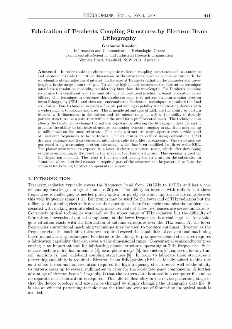
The electron beam lithography instrument comprises a purpose built pattern exposure systeminterfaced to a modified LEO 440 scanning electron microscope (SEM) [9]. A photograph of theinstrument is shown in Figure 1. The SEM has been modified with the addition of beam blankingplates and interface electronics and software to enable external control of the objective lens, beamdeflection coils and sample stage of the SEM [10].
Figure 1: Electron beam lithography instrument.
In order to accommodate a variety of substrate materials and sample types a sample holderwhich can accommodate wafers of 2, 3 or 4 inch diameters and mask plates of 4 inches has beenfitted to the sample stage of the SEM.
The entire instrument is controlled from the console which comprises both SEM and lithographycomputers. The SEM computer is used to configure the electron optics, control the vacuum systemand provide interactive imaging functions. The lithography computer is used to prepare the patterndata files, sequence the lithography functions and control the dedicated lithography electronics. Thepattern exposure system comprises the dual processor architecture of the lithography computer(PC) and digital signal processor (DSP) system, together with the associated analog and digitalelectronics [11].
The lithography PC provides the user interface for controlling and sequencing all the high levellithography functions and for controlling the sample stage and focus adjustment during lithographyoperation. The pattern data is also prepared and converted into data files suitable for exposureusing software running on the lithography PC. The lithography pattern data files provide the inputto dedicated DSP code which calculates in real time the low level pattern digital data. This digitaldata is converted into analog signals by a pair of digital to analog converters. The analog signals arethen further conditioned by low noise amplifiers before being directly applied to the beam deflectioncoils on the SEM. The DSP affords full digital control of the beam so that it may be accuratelypositioned anywhere within the field of view. The rate at which the beam is deflected is under thecontrol of the DSP to ensure that accurate doses may be delivered to the sample during exposure.
To ensure that the beam remains at the optimal focus during pattern exposure a focus planefitting algorithm has been incorporated into the exposure system. This algorithm uses the focusvalues obtained at three positions on the sample to determine the equation of the plane whichdescribes the motion of the sample. This plane fitting technique is used to calculate the correctfocus value at each position. The focus values are automatically used to directly adjust the SEMobjective lens current as the stage is moved so that the correct focus is maintained at all points onthe sample.

PIERS ONLINE, VOL. 4, NO. 4, 2008 443
3. PATTERN PREPARATION
Conventional EBL pattern generators are usually designed for exposing rectangular structures andso are typically configured for patterning horizontal or vertical lines. Some of the more interestingantenna structures require detailed curves or angular structures and may include a large variety oflinewidths. This poses an interesting challenge in converting THz structures into pattern data filesthat may be exposed using the EBL pattern generator. In order to define the structures a numberof 2D CAD drawing packages are available. These packages are able to output the design in avariety of file formats. The dxf format was chosen as it is an ASCII file and so can be examinedmanually. Software was written to convert the dxf file into the EBL lithography files. A number oftest structures have been designed using AutoCAD and successfully converted into EBL data files.An additional feature of the software is an exposure ordering tool that sequences the elements ofthe exposure file to minimise the distance the beam has to move between exposure points. Thishelps reduce artifacts associated with the beam settling time during the exposure of structureswhich contain many elements.
4. FABRICATION PROCESS
Once the planar THz structure has been defined and converted into an EBL exposure file it is readyto be patterned. The fabrication sequence involves initially spin coating the substrate with 400 nmthick layer of Polymethylmethacrylate (PMMA) electron sensitive resist. The patterns are exposedwith a beam energy of 30 kV with the sample at a working distance of 15 mm. After exposure thesample is developed in a solution of 1 Methyl Isobutyl Ketone (MIBK) : 3 Isopropyl Alcohol (IPA)for 5 minutes. After development the openings in the resist appear where the beam has exposed.These resist openings provide the mask for the evaporation of 20 nm of titanium and then 200 nmof gold. The resist layer is removed in acetone leaving the THz coupling structure on the substrate.An example of a double spiral pattern antenna structure fabricated using this technique is shownin Figure 2.
Figure 2: Double spiral antenna structure patterned by electron beam lithography.
5. CONCLUSIONS
Electron beam lithography is a valuable tool for patterning structures designed to interact withelectromagnetic radiation in the THz range. It has the principle advantages of a resolution capa-bility which is suitable for the highest THz frequencies and also the ability to pattern structureswith a wide range of dimensions. Furthermore as the patterns are defined as files on a computerit affords the possibility to create and experiment with a wide range of designs without the needfor fabricating a separate exposure mask. As a consequence structures with a variety of topologiessuitable for coupling THz radiation over a wide range of frequencies may be fabricated.

PIERS ONLINE, VOL. 4, NO. 4, 2008 444
REFERENCES
1. Siegel, P. H., “Terahertz technology,” IEEE Transactions on Microwave Theory and Tech-niques, Vol. 50, No. 3, 910–928, 2002.
2. Hu, B. B. and M. C. Nuss, “Imaging with terahertz waves,” Optics Letters, Vol. 20, No. 16,1995.
3. Seibert, K. J., H. Quast, R. Leonhardt, T. Loffer, M. Thomson, T. Bauer, H. G. Roskos, andS. Czash, “Continuous-wave all-optoelectronic terahertz imaging,” Appl. Phys. Lett., Vol. 80,3003–3005, 2002.
4. Hesler, J. L., H. Kai, R. K. Dahlstrom, R. M. Weikle, T. W. Crowe, C. M. Mann, and H. B. Wal-lace, “Analysis of an octagonal micromachined horn antenna for submillimeter-wave applica-tions,” IEEE Transactions on Antennas and Propagation, Vol. 49, No. 6, 2001.
5. Wei, A., M. Lee, and Q. Hu, “Real-time, continuous-wave terahertz imaging by use of amicrobolometer focal plane array,” Optics Letters, Vol. 30, No. 19, 2005.
6. Burns, M. J., A. W. Kleinsasser, K. A. Delin, R. P. Vasquez, B. S. Karasik, W. R. McGrath, andM. Gaidis, “Fabrication of high-Tc hot-electron bolometric mixers for terahertz applications,”IEEE Transactions on Applied Superconductivity, Vol. 7, 3564–3567, 1997.
7. Ariyoshi, S., C. Otani, A. Dobroiu, H. Sato, K. Kawase, H. M. Shimizu, T. Taino, and H. Mat-suo, “Terahertz imaging with a direct detector based on superconducting tunnel junctions,”Appl. Phys. Lett., Vol. 88, 203503, 2006.
8. Van der Weide, D. W., “Planar antennas for all-electronic terahertz systems,” J. Opt. Soc.Am. B, Vol. 11, No. 12, 1994.
9. Rosolen, G. C., “Optically variable devices fabricated by electron beam lithography,” Proc.SPIE, Vol. 5276, 318–323, 2003.
10. Rosolen, G. C., “Combined optical and electron beam lithography for integrated circuit fabri-cation,” Lithography for Semiconductor Manufacturing, Proc. SPIE, Vol. 4404, 238–244, 2001.
11. Rosolen, G. C., “Automatically aligned electron beam lithography on the nanometre scale,”Applied Surface Science, Vol. 144–145, 467–471, 1999.