false tin whiskers: masquerading tin copper intermetallics · false tin whiskers: masquerading tin...
TRANSCRIPT

FALSE TIN WHISKERS: MASQUERADING TIN COPPER INTERMETALLICS
David Hillman Rockwell Collins Inc.
Cedar Rapids, IA, USA [email protected]
ABSTRACT The electronics industry is undergoing a materials evolution due to the Restriction of Hazardous Substances (RoHS) European Directive. Printed wiring board laminate suppliers and component fabricators have introduced a number of new lead-free (Pbfree) material choices in an effort to be compliant with the EU legislation. Pure tin component surface finishes have been introduced as one of the RoHS material solutions. Tin whiskers are metallurgical phenomena that are associated with tin rich/pure tin materials and have been a topic of intense industry interest. In this study, the misidentification of tin/copper intermetallic structures as tin whiskers and the soldering process details identified during the root cause analysis of the structures will be described. Key words: Tin Whiskers, tin surface finishes BACKGROUND Tin whiskers are metallurgical phenomena that are associated with tin rich/pure tin materials and are currently a topic of intense industry interest due to the implementation of the Restriction of Hazardous Substances (RoHS) European Union (EU) Directive. The electronics industry has documented several tin whisker issues associated with components and fabricated mechanical parts (i.e. covers, heat sinks, shields, and signal fences) [1-6]. Tin whisker issues are often the result of improper plating process controls. Tin whiskers can cause electrical shorts in electronic products [7]. In March of 2007, a Rockwell Collins assembly auditor notified a process industrial engineer of whisker-like anomalies on a Quad Flat Pack (QFP) component. Figure 1 illustrates the printed wiring assembly and QFP component. Optical inspection of the QFP component revealed a large quantity of anomalies that appeared to be tin whiskers. Figure 2 illustrates the anomalies observed during the inspection.
Figure 1. Printed Wiring Assembly and Anomaly Location on QFP
Figure 2. Anomalies Observed During Optical Inspection of QFP (Top); Magnified Optical View of Anomalies (Bottom) OBJECTIVE The objective of the investigation was to determine the root cause and identification of the whisker-like anomalies
As originally published in the SMTA International Conference Proceedings.
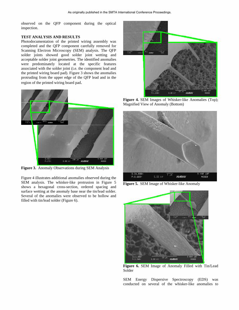
observed on the QFP component during the optical inspection. TEST ANALYSIS AND RESULTS Photodocumentation of the printed wiring assembly was completed and the QFP component carefully removed for Scanning Electron Microscopy (SEM) analysis. The QFP solder joints showed good solder joint wetting and acceptable solder joint geometries. The identified anomalies were predominately located at the specific features associated with the solder joint (i.e. the component lead and the printed wiring board pad). Figure 3 shows the anomalies protruding from the upper edge of the QFP lead and in the region of the printed wiring board pad.
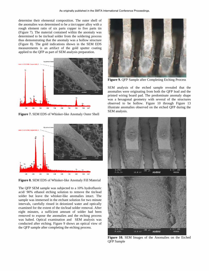
Figure 3. Anomaly Observations during SEM Analysis Figure 4 illustrates additional anomalies observed during the SEM analysis. The whisker-like protrusion in Figure 5 shows a hexagonal cross-section, ordered spacing and surface wetting at the anomaly base near the tin/lead solder. Several of the anomalies were observed to be hollow and filled with tin/lead solder (Figure 6).
Figure 4. SEM Images of Whisker-like Anomalies (Top); Magnified View of Anomaly (Bottom)
Figure 5. SEM Image of Whisker-like Anomaly
Figure 6. SEM Image of Anomaly Filled with Tin/Lead Solder SEM Energy Dispersive Spectroscopy (EDS) was conducted on several of the whisker-like anomalies to
As originally published in the SMTA International Conference Proceedings.
determine their elemental composition. The outer shell of the anomalies was determined to be a tin/copper alloy with a rough element ratio of six parts copper to five parts tin (Figure 7). The material contained within the anomaly was determined to be tin/lead solder from the soldering process thus demonstrating that the anomaly was a hollow structure (Figure 8). The gold indications shown in the SEM EDS measurements is an artifact of the gold sputter coating applied to the QFP as part of SEM analysis preparation.
Figure 7. SEM EDS of Whisker-like Anomaly Outer Shell
Figure 8. SEM EDS of Whisker-like Anomaly Fill Material The QFP SEM sample was subjected to a 10% hydrofluoric acid/ 90% ethanol etching solution to remove the tin/lead solder but leave the whisker-like anomalies intact. The sample was immersed in the etchant solution for two minute intervals, carefully rinsed in deionized water and optically examined for the extent of the tin/lead solder removal. After eight minutes, a sufficient amount of solder had been removed to expose the anomalies and the etching process was halted. Optical examination and SEM analysis was conducted after etching. Figure 9 shows an optical view of the QFP sample after completing the etching process.
Figure 9. QFP Sample after Completing Etching Process SEM analysis of the etched sample revealed that the anomalies were originating from both the QFP lead and the printed wiring board pad. The predominate anomaly shape was a hexagonal geometry with several of the structures observed to be hollow. Figure 10 through Figure 13 illustrate anomalies observed on the etched QFP during the SEM analysis.
Figure 10. SEM Images of the Anomalies on the Etched QFP Sample
As originally published in the SMTA International Conference Proceedings.

Figure 11. SEM Images of the Anomalies on the Etched QFP Sample
Figure 12. SEM Images of the Anomalies on the Etched QFP Sample
Figure 13. SEM Images of the Anomalies on the Etched QFP Sample
DISCUSSION The SEM analysis results revealed the true identity of the whisker-like anomalies observed on the printed wiring assembly. The SEM EDS results show the copper/tin element ratio of the anomalies to be approximately six parts copper to five parts tin which would correspond to the Cu6Sn5 tin/copper intermetallic (IMC) phase [8]. The Cu6Sn5 tin/copper IMC phase forms in a needle morphology as the copper content of the solder begins to exceed approximately 0.3% [9, 10]. The Cu6Sn5 intermetallic needles often form and grow preferentially from component lead and/or printed wiring pad edges. The SEM analysis shows the same behavior for the whisker-like anomalies on the QFP component. The formation and observation of Cu6Sn5 intermetallic needles solder joint microstructure is a typical occurrence. Figure 14 illustrates Cu6Sn5 IMC needles produced in a typical wave solder process solder joint. Additionally, the Cu6Sn5 intermetallic needles have a hollow, hexagonal geometry in contrast to tin whiskers which are solid striated structures that often have bends or kinks. Figure 15 illustrates a typical tin whisker compared to the Cu6Sn5 intermetallic needles observed in the investigation. Tin whiskers form and grow in random, not in an ordered orientation to each other. The typical length of the observed Cu6Sn5 IMC needles was 0.001 inches. The Cu6Sn5 IMC needles are a fixed length and do not increase over time as tin whiskers have been observed. The Cu6Sn5 IMC needles pose a minimal electrical shorting risk that would be identified during product quality testing prior to product shipment.
Figure 14. Typical Cu6Sn5 Intermetallic Needles Located in the Solder Joint Microstructure
As originally published in the SMTA International Conference Proceedings.
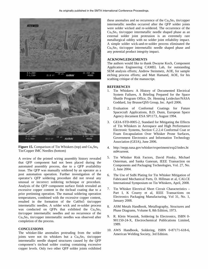
Figure 15. Comparison of Tin Whiskers (top) and Cu6Sn5
bly history reveale
anomalies protruding from the sold
he authors would like to thank Dwayne Koch, Component MEL Lab, for outstanding
. Tin Whiskers: A History of Documented Electrical res, A Briefing Prepared for the Space
ace
ance
l nd Sanka Ganesan, IEEE Transaction on
hanical Parts, D. Hillman et al, CALCE
s, Volume 8, 8th Edition, 1973.
imited,
an Welding Society, 3rd Edition.
El
Tin/Copper IMC Needles (bottom)
review of the printed wiring assemA d 5
that QFP component had not been placed during the automated assembly process, due to a QFP availability issue. The QFP was manually soldered by an operator as a post automation operation. Further investigation of the operator’s QFP soldering procedure did not reveal any unusual or incorrect soldering technique or procedure. Analysis of the QFP component surface finish revealed an excessive copper content in the tin/lead coating due to a prior pretinning operation. The manual soldering operation temperatures, combined with the excessive copper content, resulted in the formation of the Cu6Sn5 tin/copper intermetallic needles. A solder wick and re-solder process was conducted on QFPs that exhibited the Cu6Sn5 tin/copper intermetallic needles and no recurrence of the Cu6Sn5 tin/copper intermetallic needles was observed after completion of the process.
ONCLUSIONS CThe whisker-like er
1989.
10. AWS Handbook, Soldering, ISBN 0-87171-618-6, Americ
joints were not tin whiskers but a Cu6Sn5 tin/copper intermetallic needle shaped structures caused by the QFP component’s tin/lead solder coating containing excessive copper levels. Only two other QFP solder joints exhibited
these anomalies and no recurrence of the Cu6Sn5 tin/copper intermetallic needles occurred after the QFP solder joints were solder wicked and re-soldered. The occurrence of the Cu6Sn5 tin/copper intermetallic needle shaped phase as an external solder joint protrusion is an extremely rare metallurgical oddity with no solder joint reliability impact. A simple solder wick-and-re-solder process eliminated the Cu6Sn5 tin/copper intermetallic needle shaped phase and any potential product integrity impact. ACKNOWLEDGEMENTS TApplication Engineering CASEM analysis efforts; Andrew Steinmetz, AOE, for sample etching process efforts; and Matt Hamand, AOE, for his scathing critique of the manuscript. REFERENCES 1
System FailuShuttle Program Office, Dr. Henning Leidecker/NASA Goddard, Jay Brusse/QSS Group, Inc. April 2006.
2. Evaluation of Conformal Coatings for Future Spacecraft Applications, B.D. Dunn, European SpAgency document ESA SP1173, August 1994.
3. GEIA-STD-0005-2, Standard for Mitigating the Effects of Tin Whiskers in Aerospace and High Perform
ectronic Systems, Section C.2.2.4 Conformal Coat or Foam Encapsulation Over Whisker Prone Surfaces, Government Electronics and Information Technology Association (GEIA), June 2006.
4. http://nepp.nasa.gov/whisker/experiment/exp2/index.html#current.
. Tin Whisker Risk Factors, David Pinsky, MichaeOsterman, aComponents and Packaging Technologies, Vol. 27, No. 2, June 2004.
6. The Use of SnBi Plating for Tin Whisker Mitigation of Fabricated MecInternational Symposium on Tin Whiskers, April, 2008.
7. Tin Whisker Electrical Short Circuit Characteristics – Part I, K Courey et al, IEEE Transactions on Electronics Packaging Manufacturing, Vol 31, No. 1, January 2008.
8. ASM Metals Handbook, Metallography, Structures and Phase Diagram
9. R. Klein Wassink, Soldering In Electronics, ISBN 0-901150-24-X, Electrochemical Publications L
As originally published in the SMTA International Conference Proceedings.