fault tolerant network on chip design - home page...
TRANSCRIPT

Facoltà di Ingegneria Corso di Laurea in Ingegneria delle Telecomunicazioni
Fault tolerant Network on Chip (NoC) design
Relatore: Laureando:
Prof. Roberto Passerone Andrea Foradori
Correlatore:
Dr. Marcello Lajolo
Anno Accademico 2008/2009


i
Acknowledgments
Firstly of all I would like to thank my advisor, Prof. Roberto Passerone for giving me
the chance to have a studying experience abroad in an important research laboratories
as NEC Labs. He has been and is always available, as when I needed help for
delivering the request of a grant for my stay in the United States.
The same goes for my supervisor at the NEC Labs, Dr. Marcello Lajolo. He followed
me during my internship giving me important advices regarding my thesis work. I am
currently in touch with him and I really appreciate this.
I thank my father Roberto and my mother Gina for supporting me through these six
years of university. They, with my ―little‖ brother Danilo, encouraged me in many
situations of my university carrier. It is especially thanks to them that I will graduate.
Furthermore I thank Gianni for having given me material, suggestions, several
opportunities for discussions during the preparation of this thesis and for helping me
during my first weeks in USA. I also thank Peilong and Sonny with whom I lived in the
Unites States; I remember many funny situations lived together.
Finally, last but not least, I would like to thank all my friends that have stayed next to
me in these last years. Since certainly I will forget somebody if I start naming people, I
thank simply all of them but in particular Elena and Francesco that helped me during
the thesis review and have been always available for any eventuality. Moreover Elena
motivated me every time that I was in difficulty.

ii

iii
Contents
Acknowledgments ............................................................................................................. i List of Figures .................................................................................................................. v
List of Tables ................................................................................................................. vii Abstract............................................................................................................................ ix
Introduzione .................................................................................................................... xii
Glossary .......................................................................................................................... xv
Chapter 1: The Network on Chip ................................................................................. 2
1.1 NoC vs. BUS...................................................................................................... 4
1.2 NoC basic concepts overview ............................................................................ 6
1.2.1 Transport layer............................................................................................ 8
1.2.2 Network layer ........................................................................................... 10
1.2.3 Link and Physical layer ............................................................................ 21
1.3 Research Activities .......................................................................................... 22
1.4 NoC design flow .............................................................................................. 25
Chapter 2: NEC NoC.................................................................................................. 27
2.1 Topology and structure .................................................................................... 27
2.2 NoC components.............................................................................................. 32
2.2.1 AMBA AXI Network Interfaces (NIs) ..................................................... 32
2.2.2 Router ....................................................................................................... 41
2.3 NI Message encoding and Routing Algorithm ................................................ 43
2.4 Header and payload structures ......................................................................... 45
2.5 The backpressure protocol ............................................................................... 48
2.6 Pros and cons ................................................................................................... 49
Chapter 3: NoC Router redesign ................................................................................ 56
3.1 Previous Router................................................................................................ 57
3.2 The Router redesigning .................................................................................... 59
Chapter 4: Fault Tolerant NoC ................................................................................... 64
4.1 Fault tolerance and Network on Chip .............................................................. 64
4.2 How to make NoCs reliable ............................................................................. 71
4.3 Redundancy in the NEC NoC .......................................................................... 76
Chapter 5: Case study: a 5x2 tile NoC with 2 AXI Masters and 5 AXI Slaves ......... 78
5.1 Experimental platform ..................................................................................... 79

iv
5.2 The NI Sender queue selection policy............................................................. 93
5.3 Latency results................................................................................................. 99
5.4 3-master case ................................................................................................. 104
5.5 Summary ....................................................................................................... 109
Chapter 6: Conclusions and future work ................................................................. 112
Bibliography ................................................................................................................ 115
Appendix 1 ................................................................................................................... 119
Appendix 2 ................................................................................................................... 127

v
List of Figures
Figure 1.0.1 : Evolution of the cores number in a single chip .................................................................... 3 Figure 1.1.1 : Examples of communication structures in Systems-on-Chip. a) Traditional bus-based, b) dedicated point-to-point links, c) chip area network............................................................ 4 Figure 1.2.1 : 4x4 grid NoC structure ......................................................................................................... 6 Figure 1.2.2 : Layered research approach, TCP/IP stack vs. NoC stack .................................................... 7 Figure 1.2.3 : The Network Adapter........................................................................................................... 8 Figure 1.2.4 : The Network Interface hides the protocol communication to each IP core ......................... 9 Figure 1.2.5 : Typical regular network topologies ................................................................................... 10 Figure 1.2.6 : Irregular network topologies .............................................................................................. 11 Figure 1.2.7 : ST OctagonTM and ST SpidergonTM topology .................................................................... 12 Figure 1.2.8 : SpidergonTM topology layout ............................................................................................. 12 Figure 1.2.9 : Direct and indirect network ................................................................................................ 13 Figure 1.2.10 : Generic Router model ...................................................................................................... 15 Figure 1.2.11 : Units of resource allocation ............................................................................................. 16 Figure 1.2.12 : The concept of Virtual Channel (VC) .............................................................................. 17 Figure 1.2.13 : Wormhole routing deadlock example .............................................................................. 18 Figure 1.2.14 : Channel dependencies graph method ............................................................................... 19 Figure 1.2.15 : VCs Router model ............................................................................................................ 20 Figure 1.3.1 : Current NoC state of art. .................................................................................................... 23 Figure 1.3.2 : TeraFLOPS vs. ASCI Red – Source: Maurizio Palesi (Catania University, IT) ............. 24 Figure 1.4.1 : NoC design flow ................................................................................................................ 26 Figure 2.1.1 : Tile-based NoC architecture (*) ......................................................................................... 28 Figure 2.1.2 : From concentrated to distributed routers architecture ........................................................ 29 Figure 2.1.3 : Input/output routers directions ........................................................................................... 30 Figure 2.1.4 : Internal tile signals (*) ....................................................................................................... 31 Figure 2.1.5 : Block diagram of the network architecture (*) .................................................................. 31 Figure 2.2.1 : NI initiator block diagram (*) ............................................................................................ 33 Figure 2.2.2 : NI target block diagram (*) ................................................................................................ 34 Figure 2.2.3 : NI Sender architecture (*) .................................................................................................. 37 Figure 2.2.4 : FIFO architecture (*) ......................................................................................................... 39 Figure 2.2.5 : Data flow direction ............................................................................................................ 40 Figure 2.2.6 : Router architecture (*) ....................................................................................................... 42 Figure 2.3.1 : Multi-flit NoC packet format (*) ........................................................................................ 44 Figure 2.3.2 : Flit type encoding (*) ......................................................................................................... 44 Figure 2.3.3 : Supported and unsupported routing ................................................................................... 45 Figure 2.4.1 : AXI header structure (request phase) - (*) ..................................................................... 46 Figure 2.4.2 : NoC header structure (request phase) - (*) .................................................................... 46 Figure 2.4.3 : NoC header structure (response phase) - (*) .................................................................. 47 Figure 2.5.1 : Backpressure action (*) ...................................................................................................... 49 Figure 2.6.1 : Generic Input-queuing router ............................................................................................. 50 Figure 2.6.2 : Generic concentrated Virtual Output Queuing Router ....................................................... 51 Figure 2.6.3 : VOQs in the NEC NoC architecture .................................................................................. 51 Figure 2.6.4 : Used routers to reach destination: (a) standard tile-based topology, (b) NEC NoC one .... 52 Figure 2.6.5 : The connection of the Sender/Receiver with the Routers in the NEC NoC ....................... 53 Figure 2.6.6 : Wiring options ................................................................................................................... 55 Figure 3.2.1 : Modules hierarchy ............................................................................................................. 59 Figure 3.2.2 : Architecture of Router ....................................................................................................... 60 Figure 3.2.3 : RFSM states diagram ......................................................................................................... 61

vi
Figure 4.1.1 : Semiconductor Failure Rate (courtesy of M. Lajolo, NEC LA Inc.) .................................. 66 Figure 4.1.2 : CMOS technology scaling ................................................................................................. 66 Figure 4.1.3 : Failures influence the yield ................................................................................................ 67 Figure 4.1.4 : Immersion lithography ....................................................................................................... 68 Figure 4.1.5 : VLSI design variations (courtesy of M. Lajolo, NEC LA Inc.) ......................................... 69 Figure 4.1.6 : Yield loss (courtesy of M. Lajolo, NEC LA Inc.) .............................................................. 69 Figure 4.1.7 : Razor Double Data Sampling Technique ........................................................................... 70 Figure 4.2.1 : Experimental results - Source [10] ..................................................................................... 73 Figure 4.2.3 : Enable Dynamic Fault Discovery & Repartitioning (Source Intel [12]) ............................ 75 Figure 4.2.2 : Intel Larrabee (Source: [31]) .............................................................................................. 75 Figure 4.3.1 : Self-repair NoC (courtesy on NEC Labs) .......................................................................... 77 Figure 4.3.1 : Architecture evolution of NEC media chips (courtesy of M. Lajolo, NEC LA Inc.) ......... 79 Figure 5.1.1 : Experimental platform (base or standard configuration) .................................................... 80 Figure 5.1.2 : Connection between M1 and its Master Customizer in tile1 .............................................. 82 Figure 5.1.3 : End to end average packets latency from M1 @ prgn traffic ............................................. 83 Figure 5.1.4 : End to end average packets latency from M2 @ prgn traffic ............................................. 83 Figure 5.1.5 : Top level with the tiles and the latency_counter module ................................................... 84 Figure 5.1.6 : Example of end-2-end latency plot generated with GNU Plot ........................................... 86 Figure 5.1.7 : Average latencies comparison @ different injected data rate ............................................ 87 Figure 5.1.8 : Xilinx schematic file of tile1 .............................................................................................. 88 Figure 5.1.9 : General monitor setting window ........................................................................................ 88 Figure 5.1.10 : Queue utilization and backpressure graphs of the router T1_R4 (channell 0) ................. 89 Figure 5.1.11 : Standard with alternative path #1 ..................................................................................... 90 Figure 5.1.12 : Standard with alternative path #2 ..................................................................................... 91 Figure 5.1.13 : Standard with alternative path #1 and #2 ......................................................................... 92 Figure 5.2.1 : Queue selector FSM ........................................................................................................... 96 Figure 5.2.2 : Block diagram of the algorithm implementation: at behavioral level (a) and in detail (b) 98 Figure 5.3.1 : Project sub-folders ............................................................................................................. 99 Figure 5.3.2 : Sequence of actions in order to obtain the experimental results....................................... 100 Figure 5.3.3 : Simulation parameters ...................................................................................................... 100 Figure 5.3.4 : Average end-to-end latency (from Master 1) measured in clock cycle ............................ 102 Figure 5.3.5 : Average end-to-end latency (from Master 2) measured in clock cycle ............................ 102 Figure 5.3.6 : The best NoC configuration in terms of average latency improvement ........................... 103 Figure 5.3.7 : Percentage of latency improvement ................................................................................. 104 Figure 5.4.1 : Experimental platform with one Master more, placed in Tile 3 ....................................... 106 Figure 5.4.2 : Standard vs. best configuration average latency (a), Latency improvement adopting the best configuration (b) ....................................................................................................... 108

vii
List of Tables
Table 1.1.1 : BUS vs. NoC: analysis of the advantages/drawbacks ........................................................... 5 Table 2.2.1 : FIFO flags setting conditions (*) ......................................................................................... 41 Table 3.1.1 : Synthesis results of the previous router ............................................................................... 58 Table 3.2.1 : Synthesis results of the new router redesigned .................................................................... 63 Table 5.1.1 : Comparison of the resources utilization in the several platform configurations ................. 92 Table 5.4.1 : Latency of NoC components in absence of backpressure ................................................. 105 Table 5.4.2 : Possible configurations of the experimental platform ....................................................... 106 Table 5.4.3 : Average latency value for each configuration of 3 Master / 5 Slaves platform ................. 107 Table 5.5.1 : Summary of the latency/area results (standard and best configuration) ............................ 110

viii

ix
Abstract
On-chip communication architectures are known to have a significant impact on system
performance, power dissipation and time-to-market. Therefore system designers, as
well as the research community have focused on the issue of exploring, evaluating, and
designing communication architectures to meet the targeted design goals. The
emergence of multi-core architectures and heterogeneous multiprocessor Systems-on-
Chip (MPSoCs) further underscores the importance and the criticality of a suitable on-
chip communication architecture. This should handle the ever increase volume of on-
chip communication traffic and it should operate under severe performance constraints
with limited energy and thermal budgets. On the other hand, aggressive scaling of VLSI
technology has resulted in nanoscale effects that adversely affect interconnect
performance, reliability, power dissipation, and predictability. Thus new approaches to
on-chip communication architectures need to be devised in order to overcome these
effects.
The employment of Networks on Chip (NoCs) can cope with the issues mentioned
above. NoC designs consist of a number of interconnected heterogeneous devices (e.g.,
general or special purpose processors, embedded memories, application specific
components, mixed-signal I/O cores) where communication is achieved by sending
packets over a scalable interconnection network. Many models, techniques and tools
widely used in the macro-network design field can be applied to SoC design. This

x
means that a NoC can be developed in order to satisfy quality-of-service requirements
such as reliability, performance, and energy bounds.
The variability and the ceaseless CMOS technology scaling are the main factors of
transient and permanent failures. The consequence of this is a lower yield due to
unexpected power consumption and performance. Scope for optimization is limited by
architecture and hardware structure, thus device-level solutions cannot completely
solve this problem. New design models, able to tolerate failures by operating at higher
abstraction level, are necessary. Fault Tolerant NoCs are a possible solution to the
problems mentioned above. They can cope with malfunctions by supporting multipath
communication and network reconfiguration.
This thesis explores the crucial factors that lead to faults after the manufacturing of a
chip. Moreover it analyzes the possibility to handle these defects using Fault Tolerant
NoCs. Since most of the work involved in this thesis was done during a study exchange
program at NEC Laboratories America (Princeton, USA) in System Architecture
Department, experimental results and cases study are referred to the NEC NoC
architecture. In particular Chapter 5, where a case study introduced, assumes a good
familiarity with the NEC Network-on-Chip. For this reason this architecture is
described in Chapter 2.
The rest of the thesis is organized as follow: Chapter 1 provides a broad overview of
NoC concepts, existing research projects, state of the art and basic principle of on chip
communication. In Chapter 3, the router architecture designed as part of my thesis work
is presented. The architecture is compared in terms of area and performance with
respect to the implementation that was available at the beginning of my thesis. Chapter
4 explores the concept of Fault Tolerance, analyzing the factors that induce defects. An
overview of the possible NoC solutions in order to prevent or solve faults is provided.
At the end of Chapter 4 is then introduced a possible solution for the design of a
reliable NEC NoC in case of post-manufacturing faults. Furthermore Chapter 5
explores a case study, where the NoC employs many solutions presented in the
previous chapter. Implementation details and performance results are explored.
Concluding remarks and some thoughts about the possible future works are given in
Chapter 6.
During my experience at NEC Labs I participated to more than one of the on-going
activities. At first I contributed to the design of an asynchronous router for a NoC based

xi
on the GALS (Globally Asynchronous Locally Synchronous) approach. Afterwards I
developed a new version of the synchronous router, obtaining the synthesis results
presented in Chapter 4. I contributed to the realization of a simulation platform for
training purposes and, finally, I implemented and analyzed a combination of
configurations involving spatial redundancy (multipath communication) obtaining the
experimental results that are presented in Chapter 5.

xii
Introduzione
Le architetture di comunicazione on-chip comportano un significativo impatto sulle
performance di sistema, sulla dissipazione di potenza e sul time-to-market; inoltre gli
sviluppatori di sistema, cosí come la comunitá di ricerca, sono focalizzati sui problemi
di esplorazione, stima e progettazione di architetture di comunicazione che siano in
grado di raggiungere gli obbiettivi di progetto. L’emergenza di architetture multi-core e
di System-on-Chip a multiprocessore eterogenei (MPSoCs), sottolineano, inoltre,
l’importanza e la criticitá di architetture di comunicazione on-chip appropriate. Esse
devono essere in grado di gestire il rapido incremento della quantitá globale di traffico
di comunicazione on-chip e operare sotto rigidi vincoli di performance con limiti
sull’energia e sui bilanci termici (thermal budgets). D’altra parte, il continuo progresso
delle tecnologie VLSI porta ad avere dimensioni dei transistor sempre minori. Ció
implica l’incremento di effetti indesiderati (nanoscale effects), che incidono
avversamente su performance delle interconnessioni, affidabilitá, dissipazione di
potenza e predicibilitá. Di conseguenza, con lo scopo di tener testa a questi effetti, si
necessitano nuovi approcci architetturali di comunicazione on-chip.
L’impiego di Network on Chip (NoCs) puó far fronte ai problemi sopraccitati. Il
progetto di una NoC consiste di un numero di dispositivi eterogenei interconnessi tra di
loro (per esempio: processori general/special purpose, memorie embedded, componenti
per applicazioni specifiche, core mixed-signal I/O), dove la comunicazione si ottiene
mandando pacchetti attraverso una rete di interconnessione (interconnection network)

xiii
scalable (che puó essere dimensionata). Molti modelli, tecniche e tools largamente usati
per la realizzazione di reti di comunizazione macro-scale, possono essere applicati per
il progetto di SoCs. Questo significa che una Network on Chip puó essere sviluppata
per soddisfare requisiti di Quality-of-Service, quali affidabilitá, performance e limiti
energetici.
Il fenomeno conosciuto come variability e il continuo progresso tecnologico (CMOS
scaling) sono le cause principali di guasti transitori e permanenti. Tutto ció si traduce in
una minor resa produttiva (yield) causata da consumi di potenza e performance inattese.
I possibili miglioramenti della resa sono limitati dalle strutture architetturali e
hardware, perció, soluzioni solamente a livello di dispositivo non sono in grado di
risolvere completamente queste problematiche. Sono necessari nuovi modelli di
progettazione in grado di tollerare guasti operando ad un livello di astrazione maggiore.
Le NoC tolleranti i guasti (Fault Tolerant NoC) sono una possibile soluzione ai
problemi sopraccitati. Esse possono far fronte a malfunzionamenti proveddendo
comunicazione multipercorso (ridondanza) e riconfiguazione della rete.
Questa tesi esplora i fattori cruciali che portano al manifestarsi di guasti
successivamente alla fase di fabbricazione del chip e analizza la possibilitá di gestire
questi difetti usando Fault Tolerant NoCs. Poiché il lavoro di tesi è stato fatto, durante
uno programma di studio all’estero, presso i NEC Laboratories America Inc.
(Princeton, USA) nel dipartimento di System Architecture, risultati sperimentali e ―case
study‖ fanno riferimento all’architettura NoC di NEC. In particolare il Capitolo 5, nel
quale viene esaminato un―case study‖, pressupone la conoscenza della NEC NoC. Per
questo motivo il Capitolo 2 è interamente dedicato alla descrizione di quest’ultima.
La parte rimanente della tesi è organizzata nel modo seguente. Il Capitolo 1 fornisce
una ampio sguardo generale sulle NoCs: concetti elementari, progetti di ricerca
esistenti, stato dell’arte e principi di comunicazione base sono trattati. Nel Capitolo 3
viene presentata una nuova versione di Router per la NEC NoC. Si confronta la
precedente versione con quella nuova in termini di area e di performance. Il Capitolo 4
esplora il concetto di Fault Tolerance, analizzando i fattori che producono i difetti che
si manifestano dopo la fabbricazione (post-manufacturing). Vengono prese in esame le
possibili soluzioni che si avrebbero con l’impiego NoCs. Alla fine del Capitolo 4 si
presenta una possibile soluzione per rendere affidabile la NEC NoC in presenza di
guasti. Il Capitolo 5 analizza un ―case study‖, dove la NoC include le idee proposte nel
capitolo precedente mostrando dettagli d’implementazione e risultati sperimentali. In

xiv
conclusione nel Capitolo 6 vengono fatte alcune osservazioni sul lavoro svolto e si
prendono in considerazione alcuni possibili lavori futuri.
Durante la mia esperienza presso i NEC Labs ho avuto modo di prendere parte a piú
progetti attivi in quel periodo. Inizialmente ho contribuito al progetto di un router
asincrono per una NoC basata su un approccio GALS (Glabally Synchronous Locally
Asynchronous). Successivamente ho sviluppato una nuova versione del router sincrono
ottenendo i risultati di sintesi mostrati a Capitolo 4. Ho contribuito alla preparazione di
una piattaforma di simulazione utilizata dal gruppo per scopi didattici e infine ho
implementato e analizzato un semplice caso di ridondanza spaziale (multipath
communication) ottenendo i risultati sperimentali presentati a Capitolo 5.

xv
Glossary
AMBA AXI: Advanced Microcontroller Bus Architecture (AMBA) Advanced eXtensible Interface (AXI) is the 3rd generation of ARM AMBA bus protocol. The AMBA AXI protocol is targeted at high-performance, high-frequency system designs and includes a number of features that make it suitable for a high-speed submicron interconnect. Asynchronous circuit: An asynchronous circuit is a circuit in which the parts are largely autonomous. They are not governed by a clock circuit or global clock signal, but instead need only wait for the signals that indicate completion of instructions and operations. These signals are specified by simple data transfer protocols. This digital logic design is contrasted with a synchronous circuit which operates according to clock timing signals. The asynchronous circuits have many benefits. We underline one of them, particularly referred to this thesis. It is the immunity to transistor-to-transistor variability in the manufacturing process, which is one of the most serious problems facing the semiconductor industry as dies shrink. The asynchronous circuits have also disadvantage. In particular they require people experienced in synchronous design to learn a new style. Furthermore performance analysis of asynchronous circuits may be challenging. AWK: AWK is a language for processing files of text. A file is treated as a sequence of records, and by default each line is a record. Each line is broken up into a sequence of fields, so we can think of the first word in a line as the first field, the second word as the second field, and so on. An AWK program is of a sequence of pattern-action statements. AWK reads the input a line at a time. A line is scanned for each pattern in the program, and for each pattern that matches, the associated action is executed. AWK was created at Bell Labs in the 1970s. The name AWK is derived from the family names of its authors — Alfred Aho, Peter Weinberger, and Brian Kernighan

xvi
BDL: Behavioral Design Language is a language based on C language with extensions for hardware description, developed to describe hardware at levels ranging from the algorithm level to the functional level Burn-in: Burn-in is the process by which components of a system are exercised prior to being placed in service (and often, prior to the system being completely assembled from those components). The intention is to detect those particular components that would fail as a result of the initial, high-failure rate portion of the bathtub curve of component reliability. If the burn-in period is made sufficiently long (and, perhaps, artificially stressful), the system can then be trusted to be mostly free of further early failures once the burn-in process is complete. A precondition for a successful burn-in is a bathtub-like failure rate, that is, there are noticeable early failures with a decreasing failure rate following that period. By stressing all devices for a certain burn-in time the devices with the highest failure rate fail first and can be taken out of the cohort. The devices that survive the stress have a later position in the bathtub curve (with an appropriately lower ongoing failure rate). Thus by applying a burn-in, early in-use system failures can be avoided at the expense (tradeoff) of a reduced yield caused by the burn-in process. For electronic components, burn-in is frequently conducted at elevated temperature and perhaps elevated voltage. This process may also be called heat soaking. The components may be under continuous test or simply tested at the end of the burn-in period. BUS: In computer architecture, a bus is a subsystem that transfers data between on-chip components inside a chip, between computer components inside a computer or between computers. CRC code: A cyclic redundancy check (CRC) is a non-secure hash function designed to detect accidental changes to raw computer data, and is commonly used in digital networks and storage devices such as hard disk drives. A CRC-enabled device calculates a short, fixed-length binary sequence, known as the CRC code or just CRC, for each block of data and sends or stores them both together. When a block is read or received the device repeats the calculation; if the new CRC does not match the one calculated earlier, then the block contains a data error and the device may take corrective action such as rereading or requesting the block be sent again. CWB: NEC Cyber Work Bench is a behavioral synthesis system that can be used to generate hardware implementation for a system. It takes behavioral description in Behavior Description Language (BDL) or System C as input. Then, it generates the RTL description for this input. Dopant: A dopant, also called doping agent and dope, is an impurity element added to a crystal lattice in low concentrations in order to alter the optical/electrical properties of the crystal. The addition of a dopant to a semiconductor, known as doping, has the effect of shifting the Fermi level within the material. This results in a material with predominantly negative (n type) or positive (p type) charge carriers depending on the dopant species. Pure semiconductors altered by the presence of dopants are known as extrinsic semiconductors (cf. intrinsic semiconductor). Dopants are introduced into semiconductors in a variety of techniques: solid sources, gases, spin on liquid and ion implanting.

xvii
DSM: Deep Submicron VLSI technology. DVS: Dynamic voltage scaling is a power management technique in computer architecture, where the voltage used in a component is increased or decreased, depending upon circumstances. Dynamic voltage scaling to increase voltage is known as overvolting; Dynamic voltage scaling to decrease voltage is known as undervolting. Undervolting is done in order to conserve power, particularly in laptops and other mobile devices, where energy comes from a battery and thus is limited. Overvolting is done in order to increase computer performance. FIFO: FIFO is an acronym for First In, First Out, an abstraction in ways of organizing and manipulation of data relative to time and prioritization. This expression describes the principle of a queue processing technique or servicing conflicting demands by ordering process by first-come, first-served (FCFS) behaviour: what comes in first is handled first, what comes in next waits until the first is finished, etc. FSM: A finite state machine (FSM), or simply a state machine, is a model of behavior composed of a finite number of states, transitions between those states, and actions. It is similar to a "flow graph" where we can inspect the way in which the logic runs when certain conditions are met. A finite state machine is an abstract model of a machine with a primitive internal memory. Hamming code: A Hamming code is a linear error-correcting code named after its inventor, Richard Hamming. Hamming codes can detect up to two simultaneous bit errors, and correct single-bit errors; thus, reliable communication is possible when the Hamming distance between the transmitted and received bit patterns is less than or equal to one. By contrast, the simple parity code cannot correct errors, and can only detect an odd number of errors. High Level Synthesis or Behavioral synthesis: With a goal of increasing designer productivity, research efforts on the synthesis of circuits specified at the behavioral level have led to the emergence of commercial solutions recently, which are used for complex ASIC and FPGA design. These tools automatically synthesize circuits specified at C level to a register transfer level (RTL) specification, which can be used as input to a gate-level logic synthesis flow. Today, High Level Synthesis, also known as ESL synthesis and behavioral synthesis, essentially refers to circuit synthesis from high level Languages like ANSI C/C++ or SystemC etc., whereas Logic Synthesis refers to synthesis from structural or functional description in RTL. Latency: Latency is a measure of time delay experienced in a system, the precise definition of which depends on the system and the time being measured. In digital electronic the latency of a system is measured with the number of delay clock cycle, necessary to perform the system operation. Lithography: process used to transfer pattern from the mask (reticle used in lithography to block resist exposure to the irradiation in selected areas) to the layer of resist (material sensitive to irradiation i.e. changes its chemical properties when irradiated; in the form of thin film used as a pattern transfer layer in lithographic processes in semiconductor manufacturing.) deposited on the surface of the wafer; kind of lithography depends on the wavelength of radiation used to expose resist:

xviii
photolithography (or optical lithography) uses UV radiation, X-ray lithography uses X-ray, e-beam lithography uses electron bean, ion beam lithography uses ion beam. Many-core: A many-core processor is processing system in which the number of cores is large enough that traditional multi-processor techniques are no longer efficient — this threshold is somewhere in the range of several tens of cores — and likely requires a network on chip (NoC). Metastability: Metastability in electronics is the ability of an unstable equilibrium electronic state to persist for an indefinite period in a digital system. Usually the term is used to describe a state that doesn't settle into a stable '0' or '1' logic level within the time required for proper operation. This can cause the circuit to go into an undefined state and act in unpredictable ways, so it is considered a failure mode in a digital circuit. Metastable states are believed to be inherent features of asynchronous digital systems and systems with more than one clock domain, but careful design can often make the probability of a system failing very small indeed. Metastable states do not occur in fully synchronous systems when the set-up time specifications on logic gates are satisfied. MPSoC: The multiprocessor System-on-Chip (MPSoC) is a system-on-a-chip (SoC) which uses multiple processors (see multi-core), usually targeted for embedded applications. It is used by platforms that contain multiple, usually heterogeneous, processing elements with specific functionalities reflecting the need of the expected application domain, a memory hierarchy (often using scratchpad RAM and DMA) and I/O components. All these components are linked to each other by an on-chip interconnect. These architectures meet the performance needs of multimedia applications, telecommunication architectures, network security and other application domains while limiting the power consumption through the use of specialised processing elements and architecture. Multi-core: A multi-core processor is a processing system composed of two or more independent cores. The cores are typically integrated onto a single integrated circuit die (known as a chip multiprocessor or CMP), or they may be integrated onto multiple dies in a single chip package. PDA: A personal digital assistant (PDA) is a handheld computer, also known as a palmtop computer. Newer PDAs commonly have color screens and audio capabilities, enabling them to be used as mobile phones (smartphones), web browsers, or portable media players Parity bit: A parity bit is a bit that is added to ensure that the number of bits with the value one in a set of bits is even or odd. Parity bits are used as the simplest form of error detecting code.
Pipeline: In computing, a pipeline is a set of data processing elements connected in series, so that the output of one element is the input of the next one. The elements of a pipeline are often executed in parallel or in time-sliced fashion; in that case, some amount of buffer storage is often inserted between elements.

xix
RTL: In integrated circuit design, register transfer level (RTL) description is a way of describing the operation of a synchronous digital circuit. In RTL design, a circuit's behavior is defined in terms of the flow of signals (or transfer of data) between hardware registers, and the logical operations performed on those signals. Register transfer level abstraction is used in hardware description languages (HDLs) like Verilog and VHDL to create high-level representations of a circuit, from which lower-level representations and ultimately actual wiring can be derived. RTL is used in the logic design phase of the integrated circuit design cycle. An RTL description is usually converted to a gate-level description of the circuit by a logic synthesis tool. The synthesis results are then used by placement and routing tools to create a physical layout. Logic simulation tools may use a design's RTL description to verify its correctness. Synchronous circuit: A synchronous circuit is a digital circuit in which the parts are synchronized by a clock signal. In an ideal synchronous circuit, every change in the logical levels of its storage components is simultaneous. These transitions follow the level change of a special signal called the clock. Ideally, the input to each storage element has reached its final value before the next clock occurs, so the behaviour of the whole circuit can be predicted exactly. Practically, some delay is required for each logical operation, resulting in a maximum speed at which each synchronous system can run. Logic Synthesis: Logic synthesis is a process by which an abstract form of desired circuit behavior (typically register transfer level (RTL)) is turned into a design implementation in terms of logic gates. Common examples of this process include synthesis of HDLs, including VHDL and Verilog. Some tools can generate bitstreams for programmable logic devices such as PALs or FPGAs, while others target the creation of ASICs. Logic synthesis is one aspect of electronic design automation. SoC: System-on-a-chip or system on chip (SoC or SOC) refers to integrating all components of a computer or other electronic system into a single integrated circuit (chip). It may contain digital, analog, mixed-signal, and often radio-frequency functions – all on one chip. A typical application is in the area of embedded systems. Tile: Elementary module of a NoC. It contains the IP core and the module called Network Interfaced, which splits the data in packets in order to send them on the interconnection network. VLSI: Very-large-scale integration (VLSI) is the process of creating integrated circuits by combining thousands of transistor-based circuits into a single chip. VLSI began in the 1970s when complex semiconductor and communication technologies were being developed. The microprocessor is a VLSI device. The term is no longer as common as it once was, as chips have increased in complexity into billions of transistors. Yield: in semiconductor industry synonymous with "manufacturing yield", i.e. number defining percentage of operational devices out of all devices manufactured.

CHAPTER 1: THE NETWORK ON CHIP
2 | P a g e
Chapter 1: The Network on Chip
The design of a chip is based on four distinct aspects: computation, memory,
communication and I/O. The increase of the processing power and the emergence of
data intensive applications has attracted major attention on the challenge of the
communication aspect in single-chip systems (SoC). This chapter gives an overview
of an important concept for the communication in SoC, which is known as Network
on Chip (NoC). NoC does not constitute a new explicit alternative for the intra-chip
communication, but it is a unification of on-chip communication solutions. The most
important driving factors, necessary to the development of global communication
solution, are the continue increments of the on-chip resource density and the need to
use these resources with the minimum effort. The preferred solution is to try to take
advantage of economies of scale in system design, dividing the processing resources
into smaller pieces and reusing them as much as possible inside the overall design.
With this strategy it is possible to obtain shorter design time cycles, because the
global chip development can be divided in independent sub-problem.

P a g e | 3
Figure 1.0.1 : Evolution of the cores number in a single chip
Nowadays the number of cores on a single chip is increasing quickly (see Figure
1.0.1) and the inter-core communication is becoming the bottleneck in many multi-
core platforms. For this reason there is a shift of the design focus from a traditional
processing-centric to a communication-centric one.
NoC interconnection models provide a standard global communication scheme,
which gives a design style similar to a brick-like plug-and-play, allowing good use of
the available resources and fast product design cycles.

CHAPTER 1: THE NETWORK ON CHIP
4 | P a g e
1.1 NoC vs. BUS
Figure 1.1.1 shows some examples of basic communication structures in a sample
SoC, for example, PDA. Since the introduction of the SoC concept in the 90s, the
solutions for SoC communication structures have generally been characterized by
custom designed ad hoc mixes of buses and point-to-point links. The bus builds on
well understood concepts and is easy to model. In a highly interconnected multi-core
system, however, it can quickly become a communication bottleneck. In fact, it is not
ultimately scalable, since as more units are added to it, the power usage per
communication event grows leading to higher capacitive load.
Figure 1.1.1 : Examples of communication structures in Systems-on-Chip. a) Traditional bus-based, b)
dedicated point-to-point links, c) chip area network.
For multi-master busses, the problem of arbitration is also not trivial. Table 1.1.1
summarizes the pros and cons of buses and networks. A crossbar overcomes some of
the limitations of the buses. However, it is not ultimately scalable and, as such, it is
an intermediate solution. Dedicated point-to-point links are optimal in terms of
bandwidth availability, latency, and power usage as they are designed especially for
this given purpose. Also, they are simple to design and verify and easy to model. But

1.1 NOC VS. BUS
P a g e | 5
the number of links needed increases exponentially as the number of cores increases.
For these reason it leads to area and possibly routing problems.
Bus Pros & Cons Network Pros & Cons
Every unit attached adds parasitic capacitance; therefore electrical performance degrades with growth.
- + Only point-to-point one-way wires are used, for all network sizes, thus local performance is not degraded when scaling.
Bus timing is difficult in a deep submicron process.
- + Network wires can be pipelined because links are point-to-point.
Bus arbitration can become a bottleneck. The arbitration delay grows with the number of masters.
- + Routing decisions are distributed, if the network protocol is non-centric.
The bus arbiter is a specific instance. - + The same router may be re-instantiated for all network sizes.
Bandwidth is limited and shared by all units attached.
- + Aggregate bandwidth scales with the network size.
Bus latency is wire-speed once arbiter has granted control.
+ - Internal network contention may cause high latencies.
Any bus is almost directly compatible with most available IPs, including software running on CPUs.
+ - Bus-oriented IPs need smart wrappers. Software needs clean synchronization in multiprocessor systems.
The concepts are simple and well understood.
+ - System designers need re-education for new concepts.
Table 1.1.1 : BUS vs. NoC: analysis of the advantages/drawbacks
From the point of view of design-effort, one may argue that, in small systems of less
than 20 cores, an ad hoc communication structure is viable. But, as the systems grow
and the design cycle time requirements decrease, the need for more generalized
solutions becomes pressing. For maximum flexibility and scalability, it is generally
accepted that a move towards a shared, segmented global communication structure is
needed. This notion translates into a data routing network consisting of
communication links and routing nodes that are implemented on the chip [1] [2]. In
contrast to traditional SoC communication methods outlined previously, such a
distributed communication media scales well with chip size and complexity.
Additional advantages include increased aggregated performance by exploiting
parallel operation.

CHAPTER 1: THE NETWORK ON CHIP
6 | P a g e
1.2 NoC basic concepts overview
Figure 1.2.1 shows a sample NoC structured as a 4x4 grid, which provides global
chip level communication.
Figure 1.2.1 : 4x4 grid NoC structure
Traditional parallel computers have typically homogeneous architectures, but, in
general, SoCs do not necessarily exhibit such a regular architecture. NoC-based
systems implement a very high degree of variety in composition and in traffic
diversity, in order to take into account the actual system composition in terms of
homogeneity and granularity.
The three fundamental blocks of a Networks-on-Chip are:
Network Interfaces (NI): They implement the interface by which every
single IP core connects to the NoC. Their function is to decouple computation
(the cores) from communication (the network).

1.2 NOC BASIC CONCEPTS OVERVIEW
P a g e | 7
Routing Nodes: They route data according to the chosen NoC protocol and
implement the routing strategy.
Links: Connect the nodes, providing the raw bandwidth. They may consist of
one or more logical or physical channels.
Communication on chip reuses classical networking paradigms with some specific
modifications [1] [2]. Applying classical communication standards, the NoC
community consider previously designed mechanisms, however there exists a strong
need to design new protocols and algorithms for on chip communication, which are
reliable, consuming low power and acting extremely fast.
In order to understand the research work done today in relation to NoC architectures,
it is convenient to partition the fields of NoC research into four areas: 1) system and
application, 2) network interface, 3) router and 4) physical link. Figure 1.2.2 shows
the relation between these research areas; the NoC stack, with the corresponding
components, and the TCP/IP layers are compared.
Figure 1.2.2 : Layered research approach, TCP/IP stack vs. NoC stack

CHAPTER 1: THE NETWORK ON CHIP
8 | P a g e
1.2.1 Transport layer
In macro-scale networks, the Transport layer provides transparent transfer of data
between end users, thus relieving the upper layers from any concern while providing
reliable and cost-effective data transfer. It controls the reliability of a given link
through flow control, segmentation/de-segmentation, and error control. Some
protocols are state and connection oriented. This means that the transport layer can
keep track of the packets and retransmit those that fail. The best known is the
Transmission Control Protocol (TCP).
From the NoC point of view, the Network Interface (NI) is the main component at the
Transport Layer. It interfaces the core to the network and makes communication
services transparently available with a minimum of effort from the core. It handles
the end-to-end flow control, through encapsulation of the messages generated by the
IP core. These data are broken into packets, which may or may not have information
about their destination. In the latter case there must be a path setup phase prior of the
actual packet transmission.
Figure 1.2.3 : The Network Adapter
NI is known also with the name Network Adapter (NA). In this situation the Network
Interface assumes a different mean, and often it is used to represent a part of the NA.
In particular Figure 1.2.3 shows the NA structure; the component exposes a Core
Interface (CI) to the core and a Network Interface (NI) to the network side. NA

1.2 NOC BASIC CONCEPTS OVERVIEW
P a g e | 9
decouples the core from the network, enabling the implementation of a layered
system design approach. Typically the CI of the Network Adapter is implemented to
adhere to a SoC socket standard1. The CI of the Network Adapter allows, in principle,
any IP core compliant to the given socket to be attached to the network. Furthermore,
IP cores attached to the network through different sockets can communicate together
without noticing this radical difference. Figure 1.2.4 shows an example of this.
Figure 1.2.4 : The Network Interface hides the protocol communication to each IP core
The Network Adapter performs encapsulation of the traffic for the underlying
communication media. The base tasks are packets creation in a packet based NoC,
buffer management in order to prevent network congestion, global addressing and
routing. Moreover, re-order buffering and data acknowledgement could be performed.
The design of the Network Adapter is a critical task in the overall NoC design
process. Often this component handles tasks as frequency conversion and data size
conversion between core side and network side, in order to improve flexibility.
1 Socket standards are almost always identified with some legacy bus protocols, examples are ARM AMBA Bus [16], OCP Bus [18], IBM CoreConnect [17], etc.

CHAPTER 1: THE NETWORK ON CHIP
10 | P a g e
From this point forward, the word Network Interface will be used such as
synonymous of Network Adapter, except the cases when it refers to the upper part of
NA (see Figure 1.2.3). In this situation there will be a clear explication, while in all
other cases NI and NA will be regarded as the same thing.
1.2.2 Network layer
The Network level provides the hardware support for the basic communication
primitives, in order to deliver the message from the source to the destination. It is
possible to define the Network layer using basically two concepts:
Topology, which specifies the layout and connectivity of nodes and links,
and Protocol that dictates how these nodes and links are used.
Topology
The network topology is defined by the connection pattern of the routers via the
physical links.
Figure 1.2.5 : Typical regular network topologies

1.2 NOC BASIC CONCEPTS OVERVIEW
P a g e | 11
The choice of network topology has a significant impact on the SoC
price/performance ratio. There are two basic approaches to interconnecting the
routers in a NoC: either a well-defined regular topology (see Figure 1.2.5) is used, or
the routers can be interconnected in a way that is specific to the application (irregular
topology). The latter approach is clearly more versatile in terms of the system
configurability, but it presents severe disadvantages in terms of design and
verification time and exposes SoC architects to network design issues such as
deadlock avoidance that require specific expertise.
Figure 1.2.6 : Irregular network topologies
A simple way to distinguish different regular topologies is in terms of k-ary and n-
cube, where k is the degree of each dimension and n is the number of dimensions.
The k-ary tree and the k-ary n-dimensional fat tree are two alternate regular networks
explored in NoC (see Figure 1.2.5). Most NoCs implement topologies that can be
easily laid out on a chip surface. For example, k-ary 2-cube, typical grid topologies
like mesh and torus.

CHAPTER 1: THE NETWORK ON CHIP
12 | P a g e
Figure 1.2.7 : ST OctagonTM and ST SpidergonTM topology
ST Microelectronics developed its proprietary SpidergonTM topology [19], which
promises to deliver the best trade-off between theoretical performance and the
commercial realities of the SoC market. The SpidergonTM topology is similar to a
simple polygonal ring (see Figure 1.2.5), except that each node has, in addition to
links to its clockwise and counter-clockwise neighboring nodes, a direct link to its
diagonally opposite neighbor. From a routing point of view, any packet that arrives at
a node which is not its final destination can be forwarded clockwise, counter-
clockwise or across the network to its diagonally opposite node. The schematic
SpidergonTM topology translates easily into a low-cost practical layout: Figure 1.2.8
shows an example with N=16 nodes.
Figure 1.2.8 : SpidergonTM topology layout
1.2 NOC BASIC CONCEPTS OVERVIEW
P a g e | 13
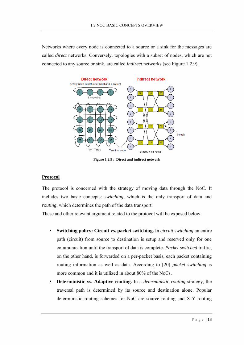
Networks where every node is connected to a source or a sink for the messages are
called direct networks. Conversely, topologies with a subset of nodes, which are not
connected to any source or sink, are called indirect networks (see Figure 1.2.9).
Figure 1.2.9 : Direct and indirect network
Protocol
The protocol is concerned with the strategy of moving data through the NoC. It
includes two basic concepts: switching, which is the only transport of data and
routing, which determines the path of the data transport.
These and other relevant argument related to the protocol will be exposed below.
Switching policy: Circuit vs. packet switching. In circuit switching an entire
path (circuit) from source to destination is setup and reserved only for one
communication until the transport of data is complete. Packet switched traffic,
on the other hand, is forwarded on a per-packet basis, each packet containing
routing information as well as data. According to [20] packet switching is
more common and it is utilized in about 80% of the NoCs.
Deterministic vs. Adaptive routing. In a deterministic routing strategy, the
traversal path is determined by its source and destination alone. Popular
deterministic routing schemes for NoC are source routing and X-Y routing

CHAPTER 1: THE NETWORK ON CHIP
14 | P a g e
(2D dimension order routing). In source routing, the source core specifies the
route to the destination. In X-Y routing, the packet follows the rows first, then
moves along the columns toward the destination or vice versa. With adaptive
routing the routing decision is taken at each hop. Adaptive mechanisms
involve dynamic arbitration mechanisms, where the arbiter takes into account
the local state of the network, for example the local link congestion. This
results in a more complex router implementation for avoiding deadlock, but
often it offers benefits like load balancing. According to [20] packet-switched
network mostly utilize deterministic routing (about 70% of cases), but some
means of adaptivity or routing policy reprogramming are necessary for fault
tolerance. Many works has been presented on this topic. An interesting one is
to split the traffic across several paths to reduce congestion on certain area of
the network [21]. Out-of-order packet delivery is in contrast with the benefits
of the adaptive routing. In many works this phenomena is totally neglected,
while others assume that the software performs the re-ordering of packets.
Minimal vs. non-minimal routing. A routing algorithm is minimal if it
chooses only among shortest paths between source and destination, otherwise
is non-minimal.
Delay vs. Loss. In the delay model, datagrams (flits, phyts1) are never lost.
The worst thing that can happen is that the arrival of data is delayed. In the
loss model instead, datagrams can be dropped. In this case means for data
retransmission are required at the level of routers, introducing significant
overhead. There are however some advantages with this model. For example
dropping flits can be used for resolving network congestion.
Central vs. distributed control. In centralized control systems routing
decision are taken globally, for example by means of an arbiter. In distributed
control instead routing decisions are made locally. NoCs usually employ the
latter solution
1 They are sub-parts of a packet. The mean of these two words will be clear in next sections.

1.2 NOC BASIC CONCEPTS OVERVIEW
P a g e | 15
The protocol defines the use of the available resources, and thus the node
implementation reflects design choices based on the aspect described above. Figure
1.2.10 shows the major components of any routing node: buffers, switch, routing and
arbitration unit and link controller. The switch connects the input buffers to the output
buffers, while the routing and arbitration unit implements the algorithm that
implements the routing policy. In a centrally controlled system, the routing and the
arbitration units would be common for all nodes.
As already mentioned, the optimal design of a router is strictly related to the services
that it has to provide. For example, support for adaptive bandwidth control can be
provided simply adding to the basic architecture of Figure 1.2.10 an additional bus,
allowing the crossbar switch to be bypassed when congestion occurs. [22]
Figure 1.2.10 : Generic Router model
The three common choices of how packets are forwarded and stored at routers are
store-and-forward, cut-through and wormhole. Before entering in details of these
techniques, we introduce the meaning of flit and phit.

CHAPTER 1: THE NETWORK ON CHIP
16 | P a g e
A message is a contiguous group of bits that is delivered from source terminal to
destination terminal. A message consists of packets, which are the basic unit for
routing and sequencing. They may be divided into flits (flow control digit), which is
the basic unit of bandwidth and storage allocation. Flits do not have any routing or
sequence information and have to follow the route for the whole packet. Instead a phit
(physical transfer digits) is the unit that is transferred across a channel in a single
clock cycle; phit and flit width could be identical. Figure 1.2.11 shows these units of
resource allocation.
Figure 1.2.11 : Units of resource allocation
Store-and-forward. It waits for the whole packet before making routing
decisions, so any node of the network stores the entire packet before
forwarding it to the next node along the route. The transmission is stalled
when the node downstream does not have sufficient space on its internal
buffers to hold the entire packet. It needs a buffering capacity for one full
packet at minimum.
Cut-through. It does not wait the whole packet, but forward this latter
already when the header information is available. The header is propagated to
the next node only if the node itself guarantees to have space enough to hold
the whole packet. Otherwise propagation is stalled and the packet is gathered
at the current node. Also for cut-through forwarding the minimum buffering
capacity has the dimension of a packet.

1.2 NOC BASIC CONCEPTS OVERVIEW
P a g e | 17
Wormhole. It is the most popular and well suited on chip. Here routing is
done as soon as possible, similar to cut-through, but the buffer space can be
smaller (only one flit at smallest). Therefore the packet may spread into many
consecutive routers and links like a ―worm‖. Latency on the single node is
significantly reduced with respect to that of store-and-forward. The major
drawback is that stalling the packet has the effect of stalling all the links
occupied by the packet along the path. In the following we will see that the
use of Virtual Channels can alleviate this problem.
Flow control
Flow Control determines how the resources of a network, such as channel bandwidth
and buffer capacity are allocated to packets traversing a network. The basic purposes
of flow control policies are to ensure correctness in the packet propagation process
and to use resources as efficiently as possible supporting a high throughput. An
efficient flow control is a prerequisite to achieve a good network performance. Flow
control primitives thus also form the basis of differentiated communication services.
In the following a selection of the topics related to flow control will be discussed.
[35]
The concept of Virtual Channels (VC) deals with the sharing of a physical channel
by several logically separated channels, which have individual and separated buffer
queues (see Figure 1.2.12).
Figure 1.2.12 : The concept of Virtual Channel (VC)

CHAPTER 1: THE NETWORK ON CHIP
18 | P a g e
Generally in NoCs, the number of VCs per physical channel varies between 2 and 16.
Usage of Virtual Channels can cause significant implementation overhead, especially
for the hardware cost of additional buffer queues and the more sophisticate control
logic of the physical channel, but it offers a number of important advantages. Among
these are:
Deadlock avoidance. Since VCs are not mutually dependent on each other,
by adding VCs to links and choosing the routing scheme properly, it is
possible to break cycles in the resource dependency graph [24].
Optimizing wire utilization. In future technologies, wire costs are projected
to dominate over transistor costs. Having several logical channels actually
using a single physical channel enables more efficient wire utilization.
Advantages include also reduced leakage power and wire routing congestion.
Improving performance. VCs are used to relax the inter-resource
dependencies in the network, thus minimizing the frequency of stalls.
According to [23], it is possible to improve the network performance at high
loads, dividing a fixed buffer size across a number of VCs.
The most important task of any flow control mechanisms is to ensure deadlock
avoidance. Deadlock can occur in an interconnection network, when a group of
packets cannot make progress, because they are waiting on each other to release
resource (buffers, channels). [35]
Figure 1.2.13 : Wormhole routing deadlock example

1.2 NOC BASIC CONCEPTS OVERVIEW
P a g e | 19
If a sequence of waiting agents forms a cycle, the network is deadlocked. We are in
presence of a deadlock if packets are allowed to hold some resources while requesting
others. Wormhole routing is particularly susceptible to deadlock. Figure 1.2.13 shows
an example of wormhole deadlock. It is possible to solve a deadlock situation by
allowing the involved packets to be preempted. Preemption packets can be:
rerouted through adaptive non-minimal routing techniques
or discarded, they are recovered at the source and retransmitted
Although it is possible to solve a deadlock, these methods are not used in most direct
networks architectures. It is more common to avoid deadlocks through the routing
algorithm, by ordering network resources and requiring that packets use these
resources in strictly monotonic order. In particular circular wait is avoided.
Figure 1.2.14 : Channel dependencies graph method
According to Duato theorem, ―A routing function R is deadlock-free if there are no
cycles in its channel dependency graph‖. So, to avoid deadlocks it is sufficient to
break cyclic dependencies in the resource dependency graph. Actually this condition
can be relaxed, as shown by [24]. It is in fact enough to require the existence of a
channel subset, which defines a connected routing sub-function with no cycles in the

CHAPTER 1: THE NETWORK ON CHIP
20 | P a g e
extended channel dependency graph. Using VCs it is sometimes possible to avoid
stalls due to packets already blocked inside the network.
Figure 1.2.15 shows a general example of router with Virtual Channels.
Figure 1.2.15 : VCs Router model
Quality of Service (QoS)
Quality of service is defined as the ability to provide different priority to different
applications, users, or data flows, or to guarantee a certain level of performance to a
data flow. For example, a required bit rate, delay, jitter, packet dropping probability
and/or bit error rate may be guaranteed. The nature of QoS, in relation to NoC, is
identified by two basic QoS classes, best-effort services (BE) which offer no
commitment, and guaranteed services (GS) which do. This latter also presents
different levels of commitment: 1) correctness of the result, 2) completion of the
transaction, 3) bounds on the performance, etc.

1.2 NOC BASIC CONCEPTS OVERVIEW
P a g e | 21
BE service refers to communication for which no commitment can be given
whatsoever. In most NoC-related works, however, BE covers the traffic for which
only correctness and completion are guaranteed, while with GS additional guarantees
are given (e.g., on the performance of a transaction). In macro-networks service
guarantees are often of statistical nature. Instead, the guarantees offered by NoC
systems are almost always hard guarantees. In order to provide them, GS
communication must be logically independent from other traffic in the system. This
requires connection-oriented routing. Connections are instantiated as virtual circuits
which use logically independent resources, thus avoiding contention. The virtual
circuits can be implemented by virtual channels, time-slots, parallel switch fabric,
etc. As the complexity of the system increases and as GS requirements grow, so does
the number of virtual circuits and resources (buffers, arbitration logic, etc) needed to
sustain them. [35]
1.2.3 Link and Physical layer
Link-level research studies the architectures of node-to-node links. These links consist
of one or more channels, which can be virtual or physical. In the following, we will
present two of the areas of interest in link-level research: 1) synchronization and 2)
implementation.
Synchronization
For link-level synchronization in a multi-clock domain SoC, the critical problem is
the FIFO design. It is very important for the multi-clock FIFOs to be particularly
robust with regards to metastability. The FIFO development can be made arbitrarily
robust with regards to metastability as settling time and latency can be traded off.
Nowadays implementing links using asynchronous circuit techniques is an obvious
possibility. This is gaining very much attention thanks to the emerging of the GALS
concept (Globally Asynchronous Locally Synchronous). In the GALS model, a
system is built putting together a number of blocks that communicate with each other

CHAPTER 1: THE NETWORK ON CHIP
22 | P a g e
one through asynchronous links, while internal communication is fully synchronous
with a given local clock. One of the major advantages of asynchronous design styles,
relevant for NoC, is the fact that, apart from leakage, no power is consumed when the
links are idle. On the other hand, asynchronous logic is necessary to implement local
handshake control. This logic implies some area and power overhead with respect to
synchronous logic. Examples of NoCs based on asynchronous circuit techniques are
CHAIN [25] and MANGO [26].
Implementation issues
As chip technologies scale into the DSM domain, the effect of wires on link delays
and power consumption increase.
A number of techniques have been proposed in the literature to improve the
performance of NoC node-to-node links in the context of DSM technology. The first
of these techniques is wire segmentation. A common solution has been for sometime
to apply repeaters at regular intervals, in order to keep the delay linearly dependent
on the length of the wire. Another technique widely used is pipelining of wire links.
In this way the link throughput is effectively increased. Use of pipelining implies
some overhead in terms of area, since pipeline stages are more complex that simple
repeaters. But as in future DSM technology wire effects tend to dominate on area
occupation, the overhead associated to pipelining is supposed to decrease.
1.3 Research Activities
The communication aspect is becoming the bottleneck in SoC architecture, both from
physical and distributed computation point of view. Wiring delays is dominating the
gate delays. In larger SoC the overall computation is heterogeneous and localized.
These factors motivate NoC, which brings the techniques developed for macro-scale
network in a single chip. NoCs have been largely reported in many papers, special

1.3 RESEARCH ACTIVITIES
P a g e | 23
journals and numerous special sessions on conferences. Therefore recently, a
dedicated NoC symposium1 has been created.
The major goal of communication-centric design and NoC paradigm is to achieve
greater design productivity and performance by handling the increasing parallelism,
manufacturing complexity, wiring problems and reliability. The three critical
challenges for NoC are power, latency and CAD (Computer Aided Design)
compatibility [20] [27].
Currently, more than 30 NoC research projects are active, both in Universities and
Industries [28]. Figure 1.3.1 shows the most important ones.
According to [28] and to [20] analysis, the chosen techniques converge to packet
wormhole switching (80% of cases), 2D mesh/torus topology (50-60%) and
deterministic routing (about 70%).
Figure 1.3.1 : Current NoC state of art.
1 www.nocsymposium.org

CHAPTER 1: THE NETWORK ON CHIP
24 | P a g e
Also asynchronous NoCs, which include GALS concepts are becoming ever more
important, as shown in the previous illustration (Figure 1.3.1), and important
universities and research institutes, such DTU (Denmark) and LETI (France), are
working on this aspect.
Network-on-Chip is a very active research field with many practical applications in
industry. Recently new NoC start-ups were born (INoCS). Furthermore the previous
start-ups are becoming successful industries (e.g., Tilera). In 2006 Intel realized a
research chip with 80 cores (160 FP engines), which communicates with a 2D mesh
interconnection network. The name of the chip is TeraFLOPS [29], since it is the first
on-chip solution able to reach the Teraflop of processing. The first computer able to
reach this performance was realized in 1996 (ASCI Red). Although only 10 years
have passed, the difference of the power consumption between ASCI Red and
TeraFLOPS are amazing (see Figure 1.3.2).
Figure 1.3.2 : TeraFLOPS vs. ASCI Red – Source: Maurizio Palesi (Catania University, IT)

1.4 NOC DESIGN FLOW
P a g e | 25
NoCs are mostly evaluated with simulation and synthesis, but should be
complemented with analytical studies and (FPGA) prototypes. The work in [20]
identifies the following topics as crucial, in order to continue the success of NoC
paradigm: procedures and test cases for benchmarking, traffic characterization and
modeling, design automation, latency and power minimization, fault-tolerance, QoS
policies, prototyping and network interface design.
1.4 NoC design flow
The ―Network-on-Chip Architecture‖ project started in 2001 and jointly conducted by
the Laboratory of Electronics and Computer Systems at the Royal Institute of
Technology and VTT, was one of the first research projects with the goal of
developing a new architecture template, called Network on chip (NoC), for future
integrated communication systems. During the workflow, the following concepts
were described: physical issues, NoC architecture with definition of communication
layers, high-level design flow methodology and working NoC simulator.
Every company (or research laboratory) develops dedicated and proprietary solutions
for creating NoC, which are used to connect and manage the communication between
the variety of design elements and intellectual property blocks required in complex
system-on-chips.
Figure 1.4.1 shows the basic concept of the NoC design flow. In the most general
case, the Design Tool provides design support both for application-specific standard
and custom network topologies, and therefore it lends itself to the implementation of
both homogeneous and heterogeneous system interconnects.

CHAPTER 1: THE NETWORK ON CHIP
26 | P a g e
Figure 1.4.1 : NoC design flow
The design flow is subdivided in three phases. In the first one, the design
requirements, necessary to specify the on-chip interconnection network, are set.
Based on these specifications, the NoC design tool generates the hardware description
of on-chip network interconnect (Verilog, VHDL, SystemC, etc), which together with
the description of the IP cores compose the whole system-on-chip (second phase). In
the last phase synthesis, floorplanning, placement and routing are performed. After
each one of this phase, there is a verification of the design constrains. In case of
negative verification, it is necessary to go back to the first phase and reset the design
parameters, in order to solve the constrain violations. In the case of NoC the common
violations that cause failed timing closure are related to the routing phase.

2.1 TOPOLOGY AND STRUCTURE
P a g e | 27
Chapter 2: NEC NoC
In this chapter we describe the NEC NoC architecture which is a configurable tile-
based Network on Chip able to scale to hundreds of IP cores. The figures marked
with the star symbol (*) are courtesy of NEC Laboratories America Inc.
2.1 Topology and structure
NEC NoC is a heterogeneous tile-based architecture where a two-dimensional fabric
of tiles is connected to form a mesh or torus architecture (Figure 2.1.1). Each tile
typically consists of one or more bus based subsystems (internal tile architecture) and
each subsystem can contain multiple IP cores (processors, memory modules and
dedicated hardware components).
The NoC tile wrapper provides access and isolation to each tile by routing and
buffering messages between tiles. The tile wrapper is connected to four other

CHAPTER 2: NEC NOC
28 | P a g e
neighboring tiles through input and output channels. A channel consists of two
unidirectional point-to-point links between two tile wrappers. A tile wrapper has
internal queues to handle congestion.
Figure 2.1.1 : Tile-based NoC architecture (*)
On the right side of Figure 2.1.1, the internal organization of a tile is shown: there are
four routers (SW1 to SW4), a receiver and a sender. Dedicated receiver and sender
units act as adaptation layers (interfaces) between the internal bus protocol and the
tile wrapper.
We can notice in Figure 2.1.1 that the NoC architecture differs from classical
concentrated one, which has a router for every tile. The NEC distributed routers
architecture can be achieved starting from a concentrated one (see Figure 2.1.2).
Firstly we imagine separating each one of the concentrated routers in four equal parts
(a single part is called distributed router). Now we can move the distributed routers,

2.1 TOPOLOGY AND STRUCTURE
P a g e | 29
which are outside the NoC, in an opposite position inside the network, in order to
obtain the final configuration.
Figure 2.1.2 : From concentrated to distributed routers architecture
The position of the switch1 both at intra-tile and inter-tile level allow one to obtain
both a mesh and a torus topology.
1 The term switch is used as a synonymous of router

CHAPTER 2: NEC NOC
30 | P a g e
Figure 2.1.3 shows the direction of input/output router connections. Each one of the
routers contained in a wrapper can reaches only one of the adjacent tiles. This involve
that every tile will be reached from four of the neighbor routers (see Figure 2.1.3).
Figure 2.1.3 : Input/output routers directions
In a wrapper, each router has four outgoing connections (see Figure 2.1.4a): outside
(0), straight (1), internal (2) and across (3), but the data path is common for all
destinations in order to save wiring. Apposite control signals, which are different for
each outgoing connection, allow the destination to understand if the delivered
information is valid or not. Similarly, each router has four incoming links (Figure
2.1.4b).

2.1 TOPOLOGY AND STRUCTURE
P a g e | 31
Figure 2.1.4 : Internal tile signals (*)
NEC NoC supports packet switching. All the messages that two IP cores have to
exchange are packetized to cross the network switch-to-switch in order to reach their
destination (see Figure 2.1.5). This technique implies contention because packet
arrival within a switch cannot be predicted; therefore arbitration mechanisms and
buffering resources must be implemented at each router.
Figure 2.1.5 : Block diagram of the network architecture (*)
CHAPTER 2: NEC NOC
32 | P a g e
AMBA AXI is used as the end-to-end communication protocol between different
cores, and the network interface takes care of protocol conversion to adapt it to the
network protocol.
The network topology is a configurable tile-based organization which gives the
designer the possibility to customize the architecture better suited for his design.
Whatever the final tile-based configuration is, the network makes use of a
deterministic source routing algorithm.
2.2 NoC components
In this section we describe all the elements shown in Figure 2.1.5 in order to give a
quick and complete overview of the NEC NoC. Major details about the NEC
Network Interface (NI) and the Routers will be explored in the next chapters.
2.2.1 AMBA AXI Network Interfaces (NIs)
The NEC NoC network interface (NI) is designed as a bridge between an AXI
interface and the NEC NoC network (as shown in Figure 2.1.5).
Its purposes are:
the packetization of AXI transactions into NEC NoC flits and vice versa, to
hide the details about the network communication protocol to the core;
the computation of routing information;
the buffering of flits (basic unit of a packet) to improve performance.
The NEC NoC NI is designed to comply with AMBA AXI specifications (3rd
generation of AMBA).
The NI hides all the details about the network communication protocol to the core.
This means that a NI must be able to read the message that one IP might want to send

2.2 NOC COMPONENTS
P a g e | 33
to another IP, build the packets to send through the network, receive the response
packets and finally decode them for the IP that generated the request.
Depending on the data flow direction, two different kinds of NIs can be identified: the
initiator (see Figure 2.2.1) and the target (see Figure 2.2.2). The NI initiator is
attached to a system master and according to its requests sends messages towards the
network. The NI target is attached to the system slave and receives messages from the
network and translates them into the AXI standard signals, so the receiver IP core can
satisfy the original requests.
The NI block can be divided further both in the vertical and the horizontal
dimensions. From the vertical point of view, it can be split into two different
channels, one for requests and one for responses. The former carries system master
commands towards slaves, while the latter provides a way for slaves to respond.
From the horizontal point of view, the NI block can be split into three stages: front-
end, queues and back-end. The front-end deals with (un-)packetization and protocol
conversion (from AXI to NEC NoC packets and vice versa), the queues provide
internal buffering and the back-end implements routing and flow control.
Figure 2.2.1 : NI initiator block diagram (*)

CHAPTER 2: NEC NOC
34 | P a g e
The NEC NoC network interface supports up to four response channels (see Figure
2.2.1) which allow the interface to avoid blocking transactions every time a request
expecting a response is issued (e.g. reads or non-posted writes).
Similarly, up to four request channels are supported at the destination (see Figure
2.2.2).
In the current implementation, request and response channels are decoupled.
Figure 2.2.2 : NI target block diagram (*)
The back-end is more strictly related to the NoC architecture, as it explicitly
communicates with its routers. It is composed of an input buffer and an output buffer,
with dual interfaces towards the network.
The NI initiator is attached to the IP core master and its task is to initiate the request
transmission and then wait for the response coming from the slave.

2.2 NOC COMPONENTS
P a g e | 35
As shown in Figure 2.2.1 it is divided horizontally into two different sub-modules to
allow a separation between the different functionalities performed, in terms of:
communication data flowing;
external supported interface (AXI or NEC NoC).
The two sub-modules are:
NI Sender: request and data flow from AXI to NEC NoC;
NI Rdata Receiver: response and data flow from NEC NoC to AXI.
The NI target is attached to the slave IP core and its task is to wait for the request
transaction coming from the master and then initiate the response transmission.
As shown in Figure 2.2.2, it is divided horizontally into two different sub-modules to
allow a separation between the different functionalities performed, in the same terms
just said for the initiator.
The two sub-modules are:
NI Receiver: request and data flow from AXI to NEC NoC;
NI Rdata Sender: response and data flow from NEC NoC to AXI.
All the following AXI transactions are provided:
Single read
Single write
Burst read
Burst write posted (the non posted is not yet supported)
A quick overview of these transactions is reported below.

CHAPTER 2: NEC NOC
36 | P a g e
SINGLE READ
Only the two header flits (NoC header and AXI header) are sent through the network,
because it is just necessary to know the path till the receiver IP and the address of the
internal memory location requested for the reading. The response packet will be
composed by the header (only the NoC header with some AXI related bits) and the
payload (containing the information read).
SINGLE WRITE
The header is not sufficient. The message itself is embodied in the payload flits. The
current implementation of a single write is posted, which means that the return
signals required by the AXI protocol are generated by the NI initiator itself, rather
than by the destination.
BURST READ
This kind of transmission is combined with the TLEN field which represents the burst
length (see Figure 2.4.1). In the read case, only the two header flits are sent across the
network, as in the single read. On the other hand, a stream of flits is generated in
response by the destination and the number of generated flits depends on the burst
length.
BURST WRITE POSTED
This kind of transmission is combined with the TLEN field which represents the burst
length. In the write case, a stream of flits is sent from the source to the destination and
the number of generated flits depends on the burst length. At the end of the
transmission, the return signals required by the AXI protocol are generated by the NI
initiator itself, rather than by the destination (posted transaction).
In this section we analyze the architecture of the only NI Sender (Figure 2.2.3).
However, is possible to see the architecture diagrams also of the other NIs, which are
reported in Appendix 1, with a summary table of the synthesis data together.

2.2 NOC COMPONENTS
P a g e | 37
Figure 2.2.3 : NI Sender architecture (*)

CHAPTER 2: NEC NOC
38 | P a g e
NI Sender supports read and write transfers from AXI to NEC NoC protocol and its
structure is shown in Figure 2.2.3.
The architecture is divided into a front-end (AXI dependent) and a back-end (NEC
NoC dependent). The following is a list of its sub-blocks.
Front-end:
get_nextQ: computes the nextQ and destination ID in case of Read/Write
transactions. The nextQ is a field of the network header. It is used by the first
Router of the Network to route the packet. In order to obtain the nextQ value
we use the same routing algorithm performed for the Router. This module has
to know with which one of the four routers the NI Sender is connected.
Get_nextQ must have this information before or at the same when the
transaction starts from the AXI Master: the Router is chosen by the
selection_logic module or is fixed at the beginning.
selection_logic: chooses transaction-by-transaction which back-end to use
(thus which Router, too). It checks the destination address (AXI signal
AWADDR or ARADRR) and computes the decision in terms of shortest
source-destination path.
rtl_func: handles the traffic coming through the AXI AW or AR channel. It
deals with the generation and delivery temporary data to the
assign_data_in_h sub-block. It manages the write control signal of the FIFO
header as well.
assign_data_in_h: assembles the temporary data signal coming from rtl_func
and from get_nextQ modules in a format suitable for the internal FIFOs.
rtl_runc_W: handles the traffic coming through the AXI W channel.
bresp_fsm_nslogic: state machine that generates the response handshake.
bresp_fsm_update: completes the state machine for the response handshake.

2.2 NOC COMPONENTS
P a g e | 39
Back-end:
ns_write_logic_h: handles the write pointer update for the header FIFO.
ns_write_logic_p: handles the write pointer update for the payload FIFO.
Header_FIFO: Header FIFO.
Payload_FIFO: Payload FIFO.
ns_read_logic_h: handles the read pointer update for the header FIFO.
ns_read_logic_p: handles the read pointer update for the payload FIFO.
assign_backend_signals: drives the output ports.
assign_flit_id_out: computes the flit_id signal.
bkend_ns_logic: assembles the NoC packet fetching information from the
FIFOs.
The sub-blocks (process in the Verilog code) ns_write_logic_h, Header_FIFO and
ns_read_logic_h compose the entity FIFO, which has been used to redesign the
Router (see Chapter 3: NoC Router redesign).
Figure 2.2.4 shows the FIFO architecture. It has been developed at low level in order
to obtain better performance in terms of total slack. We can notice in the figure below
that the components parts of the FIFO are as shown broken down. There is a module
for write inside the FIFO the new value and another for the read outside.
Figure 2.2.4 : FIFO architecture (*)
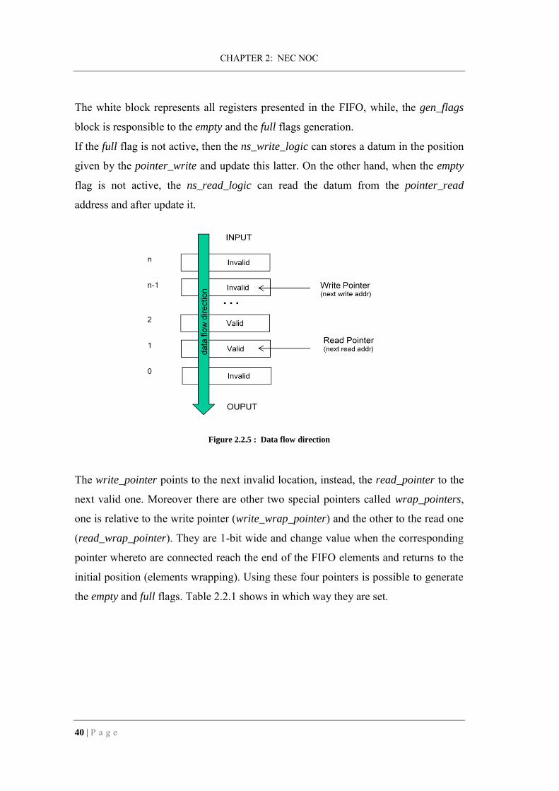
CHAPTER 2: NEC NOC
40 | P a g e
The white block represents all registers presented in the FIFO, while, the gen_flags
block is responsible to the empty and the full flags generation.
If the full flag is not active, then the ns_write_logic can stores a datum in the position
given by the pointer_write and update this latter. On the other hand, when the empty
flag is not active, the ns_read_logic can read the datum from the pointer_read
address and after update it.
Figure 2.2.5 : Data flow direction
The write_pointer points to the next invalid location, instead, the read_pointer to the
next valid one. Moreover there are other two special pointers called wrap_pointers,
one is relative to the write pointer (write_wrap_pointer) and the other to the read one
(read_wrap_pointer). They are 1-bit wide and change value when the corresponding
pointer whereto are connected reach the end of the FIFO elements and returns to the
initial position (elements wrapping). Using these four pointers is possible to generate
the empty and full flags. Table 2.2.1 shows in which way they are set.

2.2 NOC COMPONENTS
P a g e | 41
Table 2.2.1 : FIFO flags setting conditions (*)
The FIFO needs a clock cycle for data writing and a clock cycle for data reading [3].
2.2.2 Router
The NEC NoC Router implements a 4-cycle latency, input-queued router which
supports round robin arbitration on the input lines, and on-off switch-to-switch flow
control. It has four input lines and one output line and it consists of four stages:
enqueue filter, input queues, arbiter and routing logic (see Figure 2.2.6).
The enqueue filter checks the validity of the flits on all input ports and enqueues only
the valid ones. The arbiter constantly monitors the status of the queues and at every
cycle tries to send one flit to the output port of the router. Because more than one
queue might have at least one flit to send out, an arbitration step is performed. Prior
to going out, the flit dequeued by the arbiter is sent to the routing logic stage which
checks the destination coordinates and the nextQ1 fields contained in the header.
NextQ is used to set the appropriate valid bit at the output of the router, which is
associated to the outgoing direction to be taken.
The destination coordinates are used to compute the routing and update the nextQ
field in the header prior to send out the flit.
All these operations are done only on the head flit, while all subsequent flits will find
the arbiter locked and will not be modified by the routing logic.
1 NextQ identifies one of the 4 outgoing router output

CHAPTER 2: NEC NOC
42 | P a g e
Finally, the tail flit will unlock the arbiter.
Figure 2.2.6 : Router architecture (*)
An input flit can be rejected, due to one of the following reasons:
The valid bit is not set;
The buffering space for that input port is already filled.
After a packet has won the arbitration, its header flit is properly modified in order to
prepare it for the next router along the routed path to its destination. The end to end
path is chosen following a XY routing algorithm: two bits (nextQ) are used to indicate
the route of all flits of the same packet. So, the routing path from the sender to the
receiver is deterministic and is decided at the source by the NI sender.
The complexity of the router can be reduced based on the number of input ports
actually required in the system architecture. The number of input ports can vary from
1 to 4 and lower numbers correspond to a lower complexity of the arbiter, which is
actually not needed in case of one single input port.
The depth of each individual input buffer is also configurable.

2.3 NI MESSAGE ENCODING AND ROUTING ALGORITHM
P a g e | 43
2.3 NI Message encoding and Routing Algorithm
All the messages sent from an IP core can be divided into packets and the basic unit
of each packet is called flit: so, from a physical point of view, each message is
encoded by the NI into a series of flits as shown in Figure 2.3.1. The flit size is 35
bits (3 control bits and 32 data bits). The first two flits are the NoC header and the
AXI header, followed by a variable number of up to 16 payload flits. Therefore the
maximum packet size is 18 flits.
As said previously, the first two flits are header, but just the first is marked as Head.
In fact it contains NoC related information, while the second header flit carries AXI
related information. Then follow a variable number of flits containing the message
payload, the last flit of which is marked as Tail. In the case of a packet initiating an
AXI read transactions, no payload flits are sent and hence the second header flit is
marked as Tail.
NEC NoC uses wormhole routing which means that a connection is setup by the head
flit and then released by the tail flit.
When considering NoCs, it is typically observed that significant bandwidth is
available, and more can be added simply by increasing the link width. In contrast,
latency can easily grow to unacceptable levels. For these reasons, the choice of
slightly constraining the NEC NoC format was made. Instead of aiming at maximum
packing of information within the flits, this NoC uses instead a format with fixed field
offset and an immediate forwarding policy since it is more effective in terms of area
and latency. This also helps keep the amount of packing and unpacking logic low.
According to the contents, all the messages can be split into two different sections:
header and payload. The former embodies information about the sender, the receiver
and the type of transaction along with the routing information. Instead the latter
embodies the message itself.
Header and payload are never allowed to mix in the same flit, thus simplifying the
required logic.

CHAPTER 2: NEC NOC
44 | P a g e
The header is always fully transmitted while, depending on the type of transaction,
part of the payload can be useless (e.g., the AXI W wires are meaningful in a write
request, but not in a read operation), so a variable amount of payload flits may be
sent. Another difference between header and payload is that the header is present just
once, instead, the payload might be present more than once if the transaction is a
burst one (the number of times depends on the burst length).
Figure 2.3.1 : Multi-flit NoC packet format (*)
Every flit has a Flit Type tag, which is three bit wide: valid bit (V), head bit (H) and
tail bit (T) (see Figure 2.3.2).
These tags are related to the physical sequence of flits, not to the logical packet
content they embody: thus, only the very first flit of a packet is marked Head, the
very last Tail, and everything else is Body. The minimum size of a packet is two flits,
as it is the case of packets sent from a NI initiator in case of a read request, thus it can
never happen that a flit is both the head and the tail of the packet.
Figure 2.3.2 : Flit type encoding (*)

2.4 HEADER AND PAYLOAD STRUCTURES
P a g e | 45
As said before the NEC NoC implements a wormhole routing. The selected path from
the sender to the receiver is deterministic and decided at the source by the NI sender.
In this type of routing, connections between sender and receiver is of the type
connection oriented, because the path is known a priori to transmission. The
algorithm used for routing is called XY and minimizes number of hops. This takes
place firstly by using paths with only one turn. This can be explained more
thoroughly by referring to Figure 2.3.3: in that example we have a 4x3 tiles NoC with
a Sender and a Receiver. If we imagine sending data from the Sender to the Receiver
the green are the only valid paths while the red one is invalid because it contains
more than one turn. So if the traffic is going to take X direction then Y direction,
minimization will be run on the X direction first and then on the Y axis and vice
versa.
2.4 Header and payload structures
Request phases make use both of NoC and AXI headers, while response phases
forward only the NoC header since there is less information related to the AXI
protocol and it can be packed within the NoC header itself.
The structure of the AXI header is shown in Figure 2.4.1 and it does not depend upon
the type of requested transmission.
Figure 2.3.3 : Supported and unsupported routing

CHAPTER 2: NEC NOC
46 | P a g e
Figure 2.4.1 : AXI header structure (request phase) - (*)
In the following lines there is a short explanation of all the AXI header fields:
W/R: one bit identifier of the type of transaction (0 = write transaction; 1=
read transaction);
TID: tag identifier for the read/write group of signals;
TLEN: burst length;
TSIZE: burst size;
TBRST: burst type;
TLOCK: lock type;
TCACHE: cache type;
TPROT: protection type;
Un: bits currently unused.
The structure of the NoC header for the request phase is shown in Figure 2.4.2 and it
does not depend upon the type of requested transmission, but it is different in case of
response because in this phase the AXI header is not sent and the few AXI related
bits are encoded in the NoC header.
Figure 2.4.2 : NoC header structure (request phase) - (*)
Here is a complete explanation of all the NoC header fields:

2.4 HEADER AND PAYLOAD STRUCTURES
P a g e | 47
Un: bits currently unused;
NextQ: 2 bits indicating the outgoing direction that the packet needs to take
(00: outside, 01: straight, 10: internal, 11: across);
Y: Y coordinate of the destination tile;
X: X coordinate of the destination tile;
Tile: identifier of the destination tile;
LocalAddress: address to be accessed in the destination tile.
Two bits for the Y coordinate and five bits for the X coordinate are used and hence
we the NoC support a 32x4 mesh structure. The header can also be reconfigured pre-
synthesis when the size of the mesh changes.
The structure of NoC header for the response phase is shown in Figure 2.4.3. Besides
NoC related information (NextQ, Y and X), the header carries the following AXI
related information:
RID: transaction ID;
RRESP: transaction response.
Figure 2.4.3 : NoC header structure (response phase) - (*)
No additional information is needed for the proper reconstruction of the return data
transaction, since the number of payload flits equals the number of words required to
transfer back to the master all the data read.

CHAPTER 2: NEC NOC
48 | P a g e
2.5 The backpressure protocol
The data traffic passing through the network is handled by a simple protocol, which
ensures the packets delivery from the source to the destination.
The control signals of the protocol are basically two:
The valid bit
The backpressure bit
The meaning of the valid signal has been already explained before in Section 2.3. If
the valid bit is high, then the corresponding flit can be enqueued otherwise it is
discarded. Instead, the backpressure bit task is to stall the link whenever the
corresponding Router or Receiver is busy, because it is serving another channel, or
because the bandwidth is limited by the following part of path located before the
destination.
Figure 2.5.1a represents a temporal diagram of a single input Router channel. The
figure shows the action of the backpressure bit. When it goes high the current data is
kept and the input data flow stalled. This situation can happen in the two cases said
before:
The router is serving another channel;
The bandwidth is limited by the following part of the NoC.
Analogously, the backpressure performs the same function also in the backend of the
NIs. The NoC protocol is used in three different connections as shown in Figure
2.5.1b.

2.6 PROS AND CONS
P a g e | 49
a) b)
Figure 2.5.1 : Backpressure action (*)
2.6 Pros and cons
+ VIRTUAL OUTPUT QUEUING The NEC NoC structure includes the Virtual Output Queuing (VOQ) concept. The
NEC NoC router is an input-queuing router. This means that the buffering is done
before the routing.
The memory architecture of a general NxN input-queuing router (Figure 2.6.1) is
composed by N FIFO queue, one for each input line. In every single time slot, at each
one of the N queues can coming at maximum one flit. When a flit is at the head of the

CHAPTER 2: NEC NOC
50 | P a g e
queue (or Head of Line1), it has to contend for the access to the output ports with the
(N-1) flits of other queue. In the worst case we would have N flits directed to the
same output port.
When in a single time slot, there is contention for an output, only one queue is served
in that time slot. The other queues are stalled and have to wait the next time slots. On
the other hand the flits of the stalled queues that follow the first one could be routed
because directed to other output port.
This phenomenon is known as Head of the Line Blocking and [32] demonstrates that
it limit the maximum theoretical throughput at 58.6%.
One possible solution to the Head of the Line Blocking is the Virtual Output Queuing
(VOQ). Here packets are stored at an input port according to the output port they are
destined to (Figure 2.6.2). This assumes to have N queues for each input and not just
one for each one. So, the total number of queues is N2. At every cycle the scheduler
decide which VOQ can forward the flit and configure the crossbar and all hardware
problems of memory access and throughput are solved. While in the input-queuing
routing the choice is among N HoL (Head of Line) flits, for the virtual-output-
queuing it is among N2. Thus the complexity of the crossbar increases significantly.
1 The first packet of each queue is called Head of Line
Figure 2.6.1 : Generic Input-queuing router

2.6 PROS AND CONS
P a g e | 51
The distributed router NEC NoC architecture copes with this complexity. In fact each
distributed router has N input queues and this results in a much simpler scheduler
module.
Figure 2.6.2 : Generic concentrated Virtual Output Queuing Router
Figure 2.6.3 : VOQs in the NEC NoC architecture

CHAPTER 2: NEC NOC
52 | P a g e
+ FEWER NUMBER OF HOPS The NEC NoC topology compared to the generic tile-based one is able to save
basically one hop among the path sender- receiver. In order to understand this benefit
we consider the example in the following figure.
Figure 2.6.4 : Used routers to reach destination: (a) standard tile-based topology, (b) NEC NoC one

2.6 PROS AND CONS
P a g e | 53
Looking at Figure 2.6.4, we notice that in a NEC NoC the effective number of used
routers is always lower than in a generic tile-based NoC. This usefulness is derived
from the possibility to use any of the four routers contained in a tile for the
connection with the NI Sender and analogously the possibility to use four of the
twelve neighbor routers of a tile for the NI Receiver connection (see Figure 2.6.5).
Figure 2.6.5 : The connection of the Sender/Receiver with the Routers in the NEC NoC
That is not possible in a generic tile-based architecture because normally the IP cores
are connected only with one of the four neighbor routers (Figure 2.6.4).
+ MULTICAST and BROADCAST The NEC NoC lends itself to a broadcast and multicast data sending. Multicast is not
yet implemented at the moment, and we have a unicast data sending, but it is easy to
extend the architecture in order to have the other kind of sending. Going back to
Section 2.1, recall that a router has four possible destinations but they share the same
output data path (in order to save wiring). Since to choose the destination we have to
set one of the four valid bits (see Figure 2.1.4) we can think of setting all output valid

CHAPTER 2: NEC NOC
54 | P a g e
bits to high logic level in order to obtain the broadcast sending, or more than one
valid bit to high level to obtain the multicast.
Naturally, it will be necessary to include in the NoC header flit the appropriate
information to execute this kinds of sending.
+ OTHER BENEFIT OF THE DISTRIBUTED ROUTER ARCHITECTURE
With the distributed routers architecture we have a flexible ―physical architecture
easy to be reconfigurable into multiple ―logical topologies‖ and a high predictability
of the inter-tile signals. Furthermore this kind of structure enables the independent
design of every tile:
Frequency selection (local clock generator)
Voltage selection (individual power ring)
Therefore it naturally leads to hierarchical layout:
Multi-frequency design
GALS (Globally Synchronous Local Asynchronous)
– ACROSS LINK IS LONGER THAN THE OTHERS Another ―drawback‖ of the NEC NoC regards the across link. It is in fact physically
longer that the other. That could compromise the regularity of the NoC and introduce
clock skew issues.
Basically, we can consider two application field of it:
MPSoCs (Multi Processor System on Chips): they are characterized by a high
level of customization. For this reason is a good direction limit the links
number and the router complexity. In this situation it is better avoid to use the
right routing, thus it is reasonable to remove the across link in order to
simplify the NoC.
CMPs (Chip Multi Processors): a CMP is characterized by a high regularity.
In this case we can think to preserve the across link, using a homogeneous

2.6 PROS AND CONS
P a g e | 55
version of NEC NoC architecture, where each link has an equal length.
However this will results in a total wire length major than a concentrated
router NoC architecture.
Figure 2.6.6 : Wiring options

CHAPTER 3: NOC ROUTER REDESIGN
56 | P a g e
Chapter 3: NoC Router redesign
In the first months at the NEC Labs I worked for a short period of time to redesign
the router architecture. At that moment, the router was the only component of the
network that was implemented at a level higher than all the other ones. In particular,
it was written in BDL code (Behavioral Design Language). This kind of language
allows writing hardware code in ―C-like‖ mode, and the RTL version of the
behavioral router representation was obtained using a behavioral synthesis system,
called Cyber Work Bench (CWB). It takes hardware behavioral description in BDL
as input and generates the RTL description in VHDL or Verilog. [REF]
Using some modules already designed and included in the NIs, I developed a new
version of the router directly at RTL level. Although the new router improved the
performance, it has been the starting point of the RTL version and in the future will
be updated and improved again. However it is important to underline that with this
step all the NoC architecture has been described at RTL level in Verilog code.
In this phase of my job I used Modelsim to simulate and debug the hardware code
and Synopsys Design Compiler, with the NEC CB-90 library (90 nm) [34], to
synthesize it to gate level.

3.1 PREVIOUS ROUTER
P a g e | 57
3.1 Previous Router
As discussed, this previous version of the router was described and developed in
BDL. BDL is based on C language with extensions for hardware description, and was
developed to describe hardware at levels ranging from the algorithmic level to the
functional level. BDL is relatively easy to learn because it is based on a well-known
programming language.
In order to describe hardware, BDL extends the C language with the following
features, [30]:
Physical type of variable: in addition to the traditional C variables, which are
called logical variables, the BDL language integrates new types called
physical variables. They are used in order to represent hardware like
terminals, registers, ports, and so on;
Bit width: any bit width can be specified for variables in ascending or
descending order;
I/O type: these types can be used in declarations of variables for circuit inputs
and outputs. The declared variables are ―in” for input type, ―out” for output
type, and ―inout” for bidirectional (I/O) type;
Process declaration: in C, the function called "main" (hereafter referred to as
the main function) is a special function, in that this main function is always
called to start execution of a program. However, in BDL, program execution
is started by a function declared by the process declaration (hereafter referred
to as the process function). This means that each description must include a
process function;
Data transfer type: in addition to the assignment operator (=) from C, other
kinds of data transfer type have been included. The continuous assignment
(::=) method indicates a physical connection. The register transfer (<-)

CHAPTER 3: NOC ROUTER REDESIGN
58 | P a g e
method indicates assignment to the variable types that represent registers and
the terminal transfer (:=) method indicates assignment to variables, which
describe terminals;
Operators: new operators have been created in order to describe hardware
starting form C. An example is the concatenation operator, which allows one
to link variables with other variables;
Timing descriptor: it is used to specify the clock cycle boundaries;
Control statement: used to represent multiplexers;
Special constant like HiZ, used to represent high impedance.
Because the BDL level of abstraction is higher than a normal hardware language like
Verilog and VHDL, it is difficult to show a detailed block diagram of the router
architecture, but it mirrors the one represented in Figure 2.2.6.
We can obtain a Verilog description of the BDL code using a high-level synthesizer.
In particular I use a NEC tool called Cyber Work Bench (CWB) [30].
In order to have data results comparable in terms of performance and area with the
new version of the router, the achieved Verilog version has been synthesize with
Synopsis Design Compiler (using the NEC C90 library). The synthesis results of this
previous version of router are showed in the Table 3.1.1.
SYNOPSYS SYNTHESIS RESULTS
levels of
logic
critical path [ns]
clock [ns]
frequency [GHz]
cell count
area [µm2] nets VOQ
size Date
27 0.94 1.1 0.909 2,643 24,916 2,789 2 19-Feb-09
Table 3.1.1 : Synthesis results of the previous router

3.2 THE ROUTER REDESIGNING
P a g e | 59
3.2 The Router redesigning
The target is to obtain a router with the same functionality of the previous, but
developed directly at RTL level in Verilog reusing the NI FIFO queues and the NI
Round Robin Arbiter. The code reusing allows a fast developing, furthermore the
common elements inside the NIs and the Router will be the same and thus the NoC
hierarchy will become simpler and more homogeneous.
Figure 3.2.2 shows the router architecture. It is a hierarchical structure with three
modules:
Input line;
Arbiter;
Routing Logic.
The following figure (Figure 3.2.1) represents the diagram of the router hierarchy
Figure 3.2.1 : Modules hierarchy
ROUTER
INPUT LINE
FIFO
ARBITER
ROUTING LOGIC

CHAPTER 3: NOC ROUTER REDESIGN
60 | P a g e
Figure 3.2.2 : Architecture of Router
While the FIFO and the Arbiter are those of the NIs the Routing Logic has been
developed starting from that one of an asynchronous router with an appropriate
conversion from asynchronous to synchronous architecture.

3.2 THE ROUTER REDESIGNING
P a g e | 61
We need an FSM (Finite State Machine) in order to interface and synchronize the
components. Its development has been the main task of the redesign since the other
components have been reused.
I implemented the FSM using three states, one where it waits the packets arrival, one
where it operates (manage the data flits inside the queues choosing the input line
decided by the arbiter) and one for a delay necessary to the arbiter booting. The
startup state is the WAIT one.
Figure 3.2.3 shows the states diagram of the Router FSM (RFSM).
Figure 3.2.3 : RFSM states diagram
WAIT FLIT
OPERATING
BOOT
DELAY
RESET
(empty_0==”0" || empty_1==”0" ||
empty_2==”0" || empty_3==”0" ||
fetch_packet==”1")
&&
boot == ”0”
(empty_0==”0" || empty_1==”0" ||
empty_2==”0" || empty_3==”0" ||
fetch_packet==”1")
&&
boot == ”1”
header == “01”

CHAPTER 3: NOC ROUTER REDESIGN
62 | P a g e
The FSM design choice depends mainly on the arbiter: the RFSM has to wait the
arbiter decision in presence of the channel contention. So, it will have to be designed
for communicating with the arbiter packet-by-packet, in order to know which input
channel is actually active.
The arbiter monitors the requests coming from the input lines and gives the grant to
only one with a Round Robin priority policy. It starts the arbitration when a signal
called ―arbitrate‖ goes high, computes the priority count and decides which input
channel wins the contention by setting a signal called ―sel‖ with the number of the
chosen input line. At the same time it sets the signal named ―fetch_packet‖ to high
level.
The RFSM interfaces itself with the arbiter exploiting these control signals: when
there is a request (the queue is not empty) coming from one of the input lines or when
the control signal ―fetch_packet‖ is high, then the RFSM goes to the OPERATING
state. Here it sends the flit data to the Routing Logic only if there is no backpressure
coming from the connected component of the NoC. The FSM goes back to the WAIT
state when the tail flit has been sent to the Routing Logic. The router state machine
has to set the ―arbitrate‖ signal to high logic level at the correct time so that the
arbiter can handle the new request. Going back on
Figure 3.2.2 we can notice the importance of the ―sel‖ signal, it is the input of 4
processes: the RFSM, a de-multiplexer for the read control signal of the input lines
and two other multiplexers, one for the empty signal coming from the input line and
go inside the RSFM, the other for the input line data output.
The Router FSM also deals with the arbiter booting. The state machine sets a signal
called boot to high level and goes to the DELAY state only for the first contention
handled by the arbiter.
The router has been tested and debugged in several experimental platforms in order to
validate its functionality, first in a dedicated one without NIs and AXI cores,
subsequently in a real NoC platform. The router resulted fully-functional and it
replaced the previous version.

3.2 THE ROUTER REDESIGNING
P a g e | 63
In order to compare the performance of this new version with the previous one, the
Synopsys synthesis results are reported to follow in Table 3.2.1.
SYNOPSYS SYNTHESIS RESULTS
levels of
logic
critical path [ns]
clock [ns]
frequency [GHz]
cell count
Area [µm
2]
nets VOQ size
date
13 0.59 0.7 1.429 3,237 31,694 3,381 4 13-May-09
Table 3.2.1 : Synthesis results of the new router redesigned
We notice that the clock frequency increase from 0.909 to 1.429 GHz. On the other
hand also the area increases from 24,916 to 31,694 µm2, this is inevitable because the
frequency depends proportionally on area: for breaking the critical path, we need to
add new sequential logic. However the synthesis results are good enough considering
we used four buffers for the FIFO instead of two buffers like in the previous one.
Another strong point of this new router is the partial auto-configuration of the
parameters. While in the previous it was necessary to set four parameters for every
possible next tile destination (16 values), now the router deals with this computation
directly, and needs only the local position in the NoC (tile coordinates) and in the tile
(switch number). This speeds up the NoC setup and avoids manual configuration
errors.
The initial target1 has been obtained successfully. However this new version of router
has been the starting point for the direct RTL development. Although it has strong
points, like the partial auto-configuration, and increase the performance compared to
the previous one, there are also some weak points: mainly the latency, which
increased from 3 to 4 clock cycle and the level of logic that are less than of the
previous router but are still high. Starting from this version of the router, we have
then developed a new version using a simpler arbiter and which provides better
performance both in terms of latency and in terms of area utilization.
1 Obtain a router with the same functionality of the previous, but developed directly at RTL level in Verilog reusing the NI FIFO queues and the NI Round Robin Arbiter

CHAPTER 4: FAULT TOLERANT NOC
64 | P a g e
Chapter 4: Fault Tolerant NoC
In this Chapter we describe the concept of Fault Tolerance and the reason why it is
particularly connected to the NoCs.
4.1 Fault tolerance and Network on Chip
Fault-tolerance or graceful degradation is the property that enables a system to
continue operating properly in the event of the failure of (or one or more faults
within) some of its components. If its operating quality decreases at all, the decrease
is proportional to the severity of the failure, as compared to a naively-designed
system in which even a small failure can cause total breakdown.
Fault-tolerance is not just a property of individual machines; it may also characterize
the rules by which they interact. For example, the Transmission Control Protocol
(TCP) is designed to support reliable two-way communication in a packet-switched

4.1 FAULT TOLERANCE AND NETWORK ON CHIP
P a g e | 65
network, even in the presence of communications links which are imperfect or
overloaded. Within the scope of an individual system, fault-tolerance can be achieved
by anticipating exceptional conditions and building the system to cope with them,
and, in general, aiming for self-stabilization so that the system converges towards an
error-free state. [4]
Nowadays, the SoC design challenges concern at first the design complexity; the
goals are the separation of computation from communication, and the use of
structured communication means. It is also important to achieve design reliability in
order to cope with process variability, and to guarantee resilience against soft and
hard errors. Another key point is the power and thermal management; the chips
operate ever more at very low voltage level, and, a lower voltage supply is strictly
correlated with the error rates.
In this decade, many attempts have been done in order to provide a structured
methodology for realizing on chip communication in terms of modularity and
flexibility, to cope with inherent limitations of busses (performance and power of
busses do not scale up), and to support reliable operation by the use of layered
approaches to error detection and correction.
The Networks on Chip are the best means to achieve conceptual and physical
separation. NoCs are a SoC sub-system fully devoted to realize the on-chip
communication, they are reconfigurable and customizable, they can enhance error
resiliency and support array-based design and 3D integration. Furthermore they are
becoming a prerequisite as the technologies scale down, with consequent higher
system and communication complexity, higher defect and failure rates. [5]
We can distinguish three different period of time in the semiconductor life where the
failure rate changes due to several reasons. In the following figure (Figure 4.1.1) the
so-called ―bathtub‖ curve is shown, which represents the Semiconductor Failure
Rate.

CHAPTER 4: FAULT TOLERANT NOC
66 | P a g e
Figure 4.1.1 : Semiconductor Failure Rate (courtesy of M. Lajolo, NEC LA Inc.)
The Semiconductor Corporations will ceaselessly proceed CMOS scaling by
introducing various new technologies. Figure 4.1.2 shows the CMOS technology
scaling down during the current decade [6].
Figure 4.1.2 : CMOS technology scaling

4.1 FAULT TOLERANCE AND NETWORK ON CHIP
P a g e | 67
This continuous run up, toward extremely reduced transistor dimensions, involves
variations of dopants, thresholds and of geometries. At the same time, a very low
voltage level operation reduces the noise immunity, which is the reason of the soft
errors. Furthermore permanent malfunctions increase due to high temperature and to
variations of it.
All these effects are generally known as ―design variations‖. In the finer process
technologies the product yield tends to decrease due to:
Increase of systematic defects caused by fine lithography (Figure 4.1.4) and
small device inherent defect;
Increase of parametric failures caused by the higher variation sensitivity
(Figure 6.1.3).
Figure 4.1.3 : Failures influence the yield

CHAPTER 4: FAULT TOLERANT NOC
68 | P a g e
Reference: M. Lajolo, ―Toward NoC adoption at NEC‖, DATE 2009
Variations are a new challenge in LSI design. Several instances of the same chip are
different. Moreover there are variations also inside the chip: identical component of a
chip can be different (Figure 4.1.5).
We can distinguish two mainly sources of variations:
Manufacturing-induced variations: they can be subdivided in two sub-
categories. The systematic one regards the irregularities caused by the
lithography process. Masks are ideal and we never have a regular grid, hence
our layout will be subject to variations. The other category is called random. It
includes all the variation phenomenon at atomic level, such as random dopant
fluctuations and oxide thickness variations (at an atomic point of view the
transistor is not flat but it is characterized by steps).
Operation-induced variations: they appear during the operating phase of the
device. The most important are the spatial temperature variation and the
temporal voltage dropping.
Figure 4.1.4 : Immersion lithography
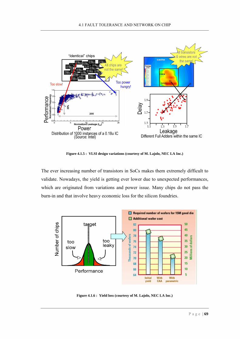
4.1 FAULT TOLERANCE AND NETWORK ON CHIP
P a g e | 69
Figure 4.1.5 : VLSI design variations (courtesy of M. Lajolo, NEC LA Inc.)
The ever increasing number of transistors in SoCs makes them extremely difficult to
validate. Nowadays, the yield is getting ever lower due to unexpected performances,
which are originated from variations and power issue. Many chips do not pass the
burn-in and that involve heavy economic loss for the silicon foundries.
Figure 4.1.6 : Yield loss (courtesy of M. Lajolo, NEC LA Inc.)

CHAPTER 4: FAULT TOLERANT NOC
70 | P a g e
E.g., for 15 million good units, we have a 20% of yield loss. That entails $ 25 million
extra cost (Figure 4.1.6). [7]
The Networks on Chip can be made resilient to errors, and can compensate
malfunctions in computing/storage elements by supporting multi-path communication
and reconfiguration. They can extend the SoC life by supporting communication
redundancy and network reconfiguration
With the presence of the NoC, we can handle the defect immunity and the error
resilience directly on-line. This is a new paradigm: it is not necessary attempt to make
an almost perfect design, but we can tolerate the malfunctions by operating at higher
abstraction levels.
The conventional ―worst case‖ design model is too conservative, there is too high
overhead in order to reach the target performance, and, the device-level solutions
cannot completely solve this problem. We need “variation-aware‖ design model in
order to achieve aggressive approaches better then worst case. Recently, self-
calibrating circuits have been developed, which operate at the edge of the failure. An
example is the concept of dynamic voltage scaling used in [8].
Figure 4.1.7 : Razor Double Data Sampling Technique
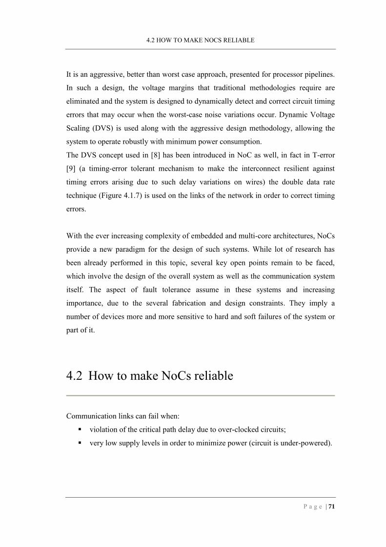
4.2 HOW TO MAKE NOCS RELIABLE
P a g e | 71
It is an aggressive, better than worst case approach, presented for processor pipelines.
In such a design, the voltage margins that traditional methodologies require are
eliminated and the system is designed to dynamically detect and correct circuit timing
errors that may occur when the worst-case noise variations occur. Dynamic Voltage
Scaling (DVS) is used along with the aggressive design methodology, allowing the
system to operate robustly with minimum power consumption.
The DVS concept used in [8] has been introduced in NoC as well, in fact in T-error
[9] (a timing-error tolerant mechanism to make the interconnect resilient against
timing errors arising due to such delay variations on wires) the double data rate
technique (Figure 4.1.7) is used on the links of the network in order to correct timing
errors.
With the ever increasing complexity of embedded and multi-core architectures, NoCs
provide a new paradigm for the design of such systems. While lot of research has
been already performed in this topic, several key open points remain to be faced,
which involve the design of the overall system as well as the communication system
itself. The aspect of fault tolerance assume in these systems and increasing
importance, due to the several fabrication and design constraints. They imply a
number of devices more and more sensitive to hard and soft failures of the system or
part of it.
4.2 How to make NoCs reliable
Communication links can fail when:
violation of the critical path delay due to over-clocked circuits;
very low supply levels in order to minimize power (circuit is under-powered).

CHAPTER 4: FAULT TOLERANT NOC
72 | P a g e
From the NoC point of view, this means that some flits/packets cannot reach the
destination. So, it becomes necessary to introduce a flow control mechanism in order
to cross the failures. The most common techniques derive from the nature of NoCs, in
fact, since a NoC is a network, we can think of using the traditional mechanisms of
the standard communication networks like error detection/retransmission (―ed‖) and
error correction (―ec‖).
In error detection/retransmission, data are transferred with error detection coding (i.e.,
Parity bit and Cyclic Redundancy Check (CRC) codes). They are checked at the
destination, and, in the case of an error, upon the detection data are retransmitted
from the source. There are basically two options: end-to-end or switch-to-switch
retransmissions.
In error correction scheme the data are transferred with an error correction code (i.e.,
Hamming code). At the destination a decoder corrects the potential error.
There is the possibility to use both techniques together achieving a hybrid scheme.
In order to apply end-to-end ―ed” schemes on NoCs, Parity Check or CRC codes
have to be added to each packet/flit. CRC/Parity encoders have to be integrated into
each sender NI, and the encoded packets have to be transmitted and stored (for
retransmission). The NI Receiver will have to check for error
Ack/Nack signal to sender can be either piggybacked with response packet or
separate;
Open Core Protocol requires request-response transaction.
Moreover we need a sequence numbers (relative position) for each packet to re-order
and identify duplicate packets. A time-out mechanism will be necessary too.
Analogous consideration can be made for the switch-to-switch approach.
In [10], an architectural level support for fault tolerance is presented, which makes
use of error detection/correction mechanisms that are used in traditional macro-
networks, in order to protect the system from transient errors that occur in the
communication sub-system. This work compares the detection/correction capability,
area-power overhead and performance of the various error detection/correction

4.2 HOW TO MAKE NOCS RELIABLE
P a g e | 73
schemes enounced before. Some experimental results of [10] is reported in Figure
4.2.1 (4x4 Mesh Network, 4 flits / packet, flit size 64 bits, 200MHz clock rate).
Figure 4.2.1 : Experimental results - Source [10]
Looking at the previous figure, we notice that with an error-aware control flow it is
possible save power and improve the latency performance. Moreover, according to
[5] and [10], the end-to-end error control flow is more efficient when the length of the
links is long, thus it is suggested for multi-cycle links. While switch-to-switch is more
efficient when the link is short and the hop-count is high. Here the NI buffering may
become an issue.
In the presence of permanent failures, the approaches mentioned before can do
anything for coping with the errors. In this case the network has to support
communication redundancy, using more than one source-destination path. Another
approach is the reconfiguration of the network, which is able to cross the failure and
repair the end-to-end communication.
The NoC routing scheme can be either static or dynamic in nature. In static routing,
one or more paths are selected, at design time, for driving the traffic flows in the
NoC. In the case of dynamic routing, the paths are selected based on the current
traffic characteristics of the network. Due to its simplicity and to the fact that
application traffics can be well characterized for most SoC designs, static routing is
widely employed for NoCs. [11]

CHAPTER 4: FAULT TOLERANT NOC
74 | P a g e
New paths means more buffer and hence more network power consumption. In
particular, special buffer could be required at the destination in order to re-order the
packets. On the other hand with multi-paths there is an improvement of the end-to-
end latency performance and an even traffic spreading in the network. We know that
for most SoC designs, the NoC operating frequency can be set to match the
application requirements. In this case, reducing the traffic bottlenecks (with the use of
multipath) leads to lower required NoC operating frequency. The reduced operating
frequency is translated to lower power consumption in the NoC. That compensates
for the more power required from the redundant paths.
Verifying SoCs initial correctness and operational errors is increasingly more
difficult. That is another reason whereby fault tolerant approaches are ever more
required in SoC design. For many years in the past, the testing of the chip was the
unique method for checking the functionality: if a unit does not pass the testing phase
it was been ―throw away‖. Only recently the systems are reconfigurable and it is
possible to safe also the unit with partial error. NoCs are a new frontier for the fault
tolerant system design. They will be necessary for downscaled technologies and will
provide SoCs with fast and reliable interconnect fabrics NoC solutions.
An example of on-line solution for error checking and correction after the
manufacturing is represented by the Intel Larrabee GPU. The first Larrabee chips will
feature 32 x86 processor cores and come out in late 2009, fabricated on a 45
nanometer process. Chips with a few defective cores due to yield issues will be sold
as a 24-core version.
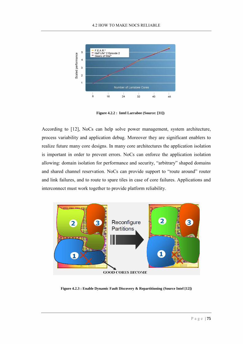
4.2 HOW TO MAKE NOCS RELIABLE
P a g e | 75
According to [12], NoCs can help solve power management, system architecture,
process variability and application debug. Moreover they are significant enablers to
realize future many core designs. In many core architectures the application isolation
is important in order to prevent errors. NoCs can enforce the application isolation
allowing: domain isolation for performance and security, ―arbitrary‖ shaped domains
and shared channel reservation. NoCs can provide support to ―route around‖ router
and link failures, and to route to spare tiles in case of core failures. Applications and
interconnect must work together to provide platform reliability.
Figure 4.2.3 : Enable Dynamic Fault Discovery & Repartitioning (Source Intel [12])
Figure 4.2.2 : Intel Larrabee (Source: [31])

CHAPTER 4: FAULT TOLERANT NOC
76 | P a g e
4.3 Redundancy in the NEC NoC
The NEC research about NoC aims at comparing the performance of a NoC solution
versus a traditional shared BUS one of commercial NEC media chips. These chips are
an evolution of older multi-core ones and the future trend is aimed at a many cores
solution. [13]
Many of today's NoC architectures are based on static single-path routing. The reason
of this choice is that with a multi-path routing, packets can reach the destination out-
of order, due to a different path length and to a different path traffic load. Many
applications do not tolerate the out-of order data delivery and, in consequence, a
packets re-ordering is necessary at the destination. Multi-processor chips requiring
data coherency are typical examples of architectures where in order packet arrival at
the destination is mandatory
The NEC NoC uses a static single-path routing where the source-destination path is
chosen at design time, in fact, it has to guarantee an in order packet delivery because
the media chips are employed in video and multimedia applications. Packet ordering
needs to be maintained for displays and for many of the processing blocks in the
application.
At the moment of my arrival at the NEC Laboratories, the NEC NoC did not employ
any form of Fault Tolerance. The target of my job has been to introduce adaptiveness
in the network adding redundant source destination paths, in order to guarantee the
communication also in the presence of permanent errors that could be discovered
post manufacturing.
The goal is to integrate post-manufacturing diagnosis and self-repair (Figure 4.3.1).
This is achieved by means of routing constraints determined based on diagnostic
feedback reporting the list of faulty links and faulty processing elements like routers.

4.3 REDUNDANCY IN THE NEC NOC
P a g e | 77
Faulty links can have an associated backpressure bit that is kept constantly high thus
resulting in the capability for the network to route the traffic through alternative
paths.
A faulty processing element like a router can also be managed in the same way since
it is sufficient to map as faulty the link just before the faulty resource in the topology
of the network. The result is the capability to sustain a satisfactory level of yield at
the cost of decreased performance.
The result is the capability to enhance the basic static single-path routing, with the
capability to ―route around‖ faults.
Constrained routing is thus a way to implement an online self-repair strategy based on
post manufacturing information.
Figure 4.3.1 : Self-repair NoC (courtesy on NEC Labs)

CHAPTER 5: CASE STUDY: A 5X2 TILE NOC WITH 2 AXI MASTERS AND 5 AXI SLAVES
78 | P a g e
Chapter 5: Case study: a 5x2 tile
NoC with 2 AXI Masters and 5 AXI
Slaves
The redundancy injected inside the NEC NoC has been thought in order to avoid chip
defect, which appear after the manufacturing phase. On the other hand, we can use
the alternative paths to increase the performance in terms of latency.
In this chapter we show the explored case study: a 5x2 tile NoC with AXI Masters
and Slaves. The NoC shape and the Processing Elements (PEs) disposition depend on
the NEC research goal on the NoCs, which aims at estimating the performance of a
NoC solution for data communication in the video-processing chips (see Figure
4.3.1).

5.1 EXPERIMENTAL PLATFORM
P a g e | 79
Figure 4.3.1 : Architecture evolution of NEC media chips (courtesy of M. Lajolo, NEC LA Inc.)
In Figure 4.3.1 we notice that the media chips PEs are disposed horizontally. For this
reason the NoC experimental platform, used as case study, inherits a common shape
with 5 horizontal tiles and 2 vertical ones.
In this phase of my thesis job, we used the following CAD tools and applications:
a text editor for the code writing;
Cyber Work Bench for the generation of the AXI masters and the slaves;
Mentor Modelsim 6.2h simulator for the functional simulations;
Synopsis Design Compiler for the components synthesis;
and Xilinx ISE 9.2i for the netlist assembling.
5.1 Experimental platform
The experimental platform (or simulation platform) is the 5x2 tile NoC shown in
Figure 5.1.1. There are 2 AXI Masters, one in tile1 (M1) and one in tile2 (M2), while
in the bottom tiles we find the AXI Slaves (SL1, 2, 3, 4, 5). Every master reaches

CHAPTER 5: CASE STUDY: A 5X2 TILE NOC WITH 2 AXI MASTERS AND 5 AXI SLAVES
80 | P a g e
every slave through the NoC, using the routers represented in the figure. The design
choice of the source-destination paths has been made in order to minimize the number
of the routers, obtaining the basic logical configuration of the NoC. It uses three 2-
input routers and five 1-input routers.
Figure 5.1.1 : Experimental platform (base or standard configuration)
The platform is able to handle single write and burst write AXI transactions. The read
transaction is not supported in fact, looking at Figure 5.1.1, we can notice that there
are no return links (NI Rdata Receiver and NI Rdata Sender missing). Although the
platform supports the only write transaction, it is a good example considering also
that no similar works have previously been done at NEC Labs.
The NEC NoC is defined at the RTL level and, at the moment, a connection with a
software application is missing. The PEs are behavioral descriptions used only for
NoC simulation purposes, this results in the impossibility to simulate a failure. For
these reasons, in this chapter several configurations of the experimental platform are
analyzed and compared in terms of latency. This assumes the presence of a re-order
5.1 EXPERIMENTAL PLATFORM
P a g e | 81
module at the destination in order to maintain the coherence of the data. The
alternative paths have been chosen in such that the number of hops, from source to
destination, is always the same for each path. Moreover with the introduction of the
redundant paths the traffic is spread on the network homogeneously. For these
reasons we have an inherent in-order delivery. The first simulations confirmed this
theory and, in order to have a simpler platform too (we recall that this is the first time
that we use a multipath routing in NEC NoC, the reorder module was not used in the
platform. However, the NoC needs it and one of the first future improvements could
concern its implementation and integration.
The developed work includes also the addition of some utilities to the NoC. One of
these is the possibility to choose among three different typologies of traffic:
single destination (only one slave);
round robin destination;
pseudo-random destination.
In order to achieve this functionality, we generated masters, via Cyber Work Bench
(CWB), in another way different from the advised one. Adding two ports to the top of
the master, it became customizable in terms of intra-packets delay and address
destination.
We developed an external Verilog module (called Master Customizer), which is able
to set the new master parameters. With this new component it is possible to choose
one of the kind of traffic shown above, while before the unique possibility was the
single-destination. Moreover with the possibility of inserting a delay among packets,
we avoid the re-generation, starting from the CWB, every time that we want a
different delay.
Operating on the delay parameter, it is possible to run simulations at different data
rate. Figure 5.1.3 and Figure 5.1.4 show latency simulation results at several data rate,

CHAPTER 5: CASE STUDY: A 5X2 TILE NOC WITH 2 AXI MASTERS AND 5 AXI SLAVES
82 | P a g e
in case of random traffic (prgn, Pseudo Random GeNerator), because it is the most
interesting. The intra-packets delay was changed with the following sequence of
values: 1000, 100, 10, 1, 0 clock cycles.
Figure 5.1.2 : Connection between M1 and its Master Customizer in tile1
Figure 5.1.3 and Figure 5.1.4 show the end to end average latencies for packets that
start from M1 and M2 respectively. On the x-axis there are the five destinations,
while along the y-axis the injected data rate, expressed in byte/s. The two graphs have
to be read together, this means that, when M1 injects 23 MB/s (see Figure 5.1.3), at
the same time M2 will inject 23 MB/s (see Figure 5.1.4) and so on for the other data
rate values.

5.1 EXPERIMENTAL PLATFORM
P a g e | 83
Figure 5.1.3 : End to end average packets latency from M1 @ prgn traffic
Figure 5.1.4 : End to end average packets latency from M2 @ prgn traffic

CHAPTER 5: CASE STUDY: A 5X2 TILE NOC WITH 2 AXI MASTERS AND 5 AXI SLAVES
84 | P a g e
We can notice naturally that the latency increases when the injected data rate grows.
The latency data have obtained by including a dedicated monitor, which saves on
files the appropriate information necessary to compute the latency. I wrote this
monitor (called latency_counter) in Verilog and I included it at top level in the netlist
(Figure 5.1.5).
Figure 5.1.5 : Top level with the tiles and the latency_counter module
Latency_counter monitors some signals of the masters and of the slaves, saving the
transition traces on file. In particular it keeps the trace of the time (clock cycle) when
a packet starts from the master X and when it reaches the slave Y. A piece of a trace
relative to packets that reach Slave 1 is shown below.

5.1 EXPERIMENTAL PLATFORM
P a g e | 85
ClockCycle: Trigger sample signal: AWADDR: WDATA:
60 WVALID_S1 00002000 16
71 WVALID_D1 00012000 16
75 WVALID_S2 00003000 48
86 WVALID_S1 00001000 64
89 WVALID_S2 00000000 80
89 WVALID_D1 00023000 48
93 WVALID_S1 00002000 80
97 WVALID_D1 00011000 64
104 WVALID_D1 00020000 80
112 WVALID_D1 00012000 80
122 WVALID_S1 00002000 144
... … … …
... … … …
Starting from these traces, with an appropriate elaboration of them, it is possible to
obtain the end-to-end latency for packets that reach Slave 1. Awk scripts for each one
of the traces generated with the Modelsim simulation have been written. These scripts
read the trace and generate the latency final results. The final format of the latency
data is compatible with GNU Plot1 for a direct plotting from file. [14] [15]
An example of the format is reported below.
##########################################
# End to end Latency MASTER_1 -> SLAVE_1 #
##########################################
#Packet_ID Latency
1 11
2 15
3 16
4 11
… …
1GNU Plot is a command-driven interactive function and data plotting program

CHAPTER 5: CASE STUDY: A 5X2 TILE NOC WITH 2 AXI MASTERS AND 5 AXI SLAVES
86 | P a g e
With these results we know the end-to-end latency of every NoC packet and we can
handle these data in the most appropriate manner. The simplest solution is the direct
plotting with GNU Plot. In this way it is possible to look at the latency of each single
packet from Master X to Slave X. As an example, Figure 5.1.6 reports the end-to-end
latency plot of the packets, which start from Master1 / Master2 and reach Slave 1.
Figure 5.1.6 : Example of end-2-end latency plot generated with GNU Plot
Another solution is to process again the data in order to plot the average latency
(examples are Figure 5.1.3 and Figure 5.1.4)
Figure 5.1.7 compares the average latency data that have been obtained with the
simulation at different data rate. Analyzing the figure we notice that the latency value
depends on the destination. E.g., in case of Master1, the average latency at SL1 and
SL2 destinations is lower than for the other slaves. This is correct, because the

5.1 EXPERIMENTAL PLATFORM
P a g e | 87
Master1 position in the platform is nearer to SL1 and to SL2 than to the other ones
(see the platform in Figure 5.1.1). Analogous situation happens for Master2.
Other kinds of monitors have been implemented. They keep trace of the FIFO buffers
utilization, of the backpressure bits value, and of the NI Sender selected queue signal.
They have been developed in Verilog. Using Xilinx ISE it is possible to connect them
to the signal under test directly, specifying the path and the name of the text file
where the trace will be saved. We named this module general_monitor, it can monitor
four FIFO buffer, four backpressure bit and one NI Sender selected queue signal
(queue_selector in the code). In the following figures, the tile1 Xilinx schematic
netlist (Figure 5.1.8) and the window where it is possible to set the monitor file
parameters (Figure 5.1.9) are shown.
11
9
13
16
18
11
9
13
16
18
11
9
13
16
18
1211
15
18
21
1312
16
20
22
SL1 SL2 SL3 SL4 SL5
from Master 1 - prgn
23 MB/s 224 MB/s 1411 MB/s
2869 MB/s 3078 MB/s
14 14
9
12
1414 14
9
12
1414 14
9
12
1415
14
10
14
1615
14
11
15
17
SL1 SL2 SL3 SL4 SL5
from Master 2 - prgn
23 MB/s 224 MB/s 1141 MB/s
2977 MB/s 3265 MB/s
Figure 5.1.7 : Average latencies comparison @ different injected data rate

CHAPTER 5: CASE STUDY: A 5X2 TILE NOC WITH 2 AXI MASTERS AND 5 AXI SLAVES
88 | P a g e
Figure 5.1.8 : Xilinx schematic file of tile1
Figure 5.1.9 : General monitor setting window
The traces obtained from the general monitors are also in this case in a format
compatible with GNU Plot. So, it is possible to plot the graphs directly from file.

5.1 EXPERIMENTAL PLATFORM
P a g e | 89
All these data could be used in order to understand which router is the busiest in the
network. Furthermore, this analysis will help us find an alternative routing solution
for relieving the work of this router. The utilization buffer traces allow us to
understand the optimal number of the FIFO elements.
The data simulation trace can to be used in many other ways. We limit ourself to
present the data results. An example is shown below.
Figure 5.1.10 : Queue utilization and backpressure graphs of the router T1_R4 (channel 0)
Starting from the standard experimental platform, I add to it alternative paths in order
to have the possibility to reconfigure the NoC, in presence of post-manufacturing
failures. As mentioned before, the benefits of these solutions depend on a
compromise between the latency and the utilized resources.
I introduced several redundant paths in the NoC in order to relieve especially the load
of routers T34_R2 and T1_R4 (see Figure 5.1.1). Basically, the alternative paths are

CHAPTER 5: CASE STUDY: A 5X2 TILE NOC WITH 2 AXI MASTERS AND 5 AXI SLAVES
90 | P a g e
two and can be used also together. So, we obtain three new configurations of the
simulation platform in addition to the standard one:
Standard (std)
Standard with alternative path 1 (alt1)
Standard with alternative path 2 (alt2)
Standard with alternative path 1 and 2 (alt1+2)
Figure 5.1.11 shows the platform with the alternative path number 1.
Figure 5.1.11 : Standard with alternative path #1
The redundant path is represented in red color. As we can notice it involves the use of
four additional 1-input routers compared to the standard configuration. Moreover it is
necessary to replace the 2-output NI Sender (two backends) of tile2, with a 3-output
one (three backends). The description of the 3-output NI Sender will be done in the
following section (5.2 - The NI Sender queue selection policy).

5.1 EXPERIMENTAL PLATFORM
P a g e | 91
Figure 5.1.12 shows the experimental platform with the alternative path number 2. It
is drawn with a violet color and it needs five 1-input routers more than standard
configuration platform and a 2-input one, which replaces the T2_R4 (1-input). Also
for this configuration is necessary to employ a NI Sender with 3 backends.
Figure 5.1.12 : Standard with alternative path #2
We can use both alternative paths together. This configuration needs four 1-input and
one 2-input routers more than standard configuration platform. Moreover, it will be
necessary to replace one 1-input router (T2_R4) with 2-input one. In Figure 5.1.13
the simulation platform with the presence of both the alternative paths together is
represented.

CHAPTER 5: CASE STUDY: A 5X2 TILE NOC WITH 2 AXI MASTERS AND 5 AXI SLAVES
92 | P a g e
Figure 5.1.13 : Standard with alternative path #1 and #2
A first comparison (in terms of resources utilized) of the several platform
configurations can be done. As we notice, the three new platform solution needs more
routers and more complex NI Sender than the standard configuration. Table 5.1.1
shows a summary of the utilized resources in the three cases.
single area
[µm2]
Standard Alternative #1 Alternative #2 Alternative #1+#2
# units
units total area
# units
units total area
# units
units total area
# units
units total area
1-in
Router 5951 5 29755 9 53559 9 53559 8 47608
2-in
Router 11142 3 33426 3 33426 4 44568 5 55710
2-out
Sender 40810 2 81620 1 40810 1 40810 - -
3-out
Sender 64888 - - 1 64888 1 64888 2 129776
1-in
Receiver 17185 4 68740 2 34370 2 34370 2 34370
2-in
Receiver 33428 1 34428 3 103284 3 103284 3 103284
Total: 247969 330337 341479 370738
Table 5.1.1 : Comparison of the resources utilization in the several platform configurations

5.2 THE NI SENDER QUEUE SELECTION POLICY
P a g e | 93
5.2 The NI Sender queue selection policy
The NI Sender queue selection policy has been implemented following two basic
ideas:
we can switch to an alternative path when the backpressure reaches the source
and then, switch back to the standard path when there is backpressure again;
or, we switch to the alternative path and switch back continuously to standard
path packet-by-packet.
These two approaches are explained in detail with Algorithm 1 and Algorithm 2 in
the next page.
DEST_RANGE_DOWN and DEST_RANGE_UP are two of the NI Sender Frontend
parameters. They define a mask of address. Packets with destination address lower
than DEST_RANGE_DOWN are routed using the backend #1. If the destination
address of a packet is between DEST_RANGE_DOWN and DEST_RANGE_UP, it is
routed using the backend #2. Instead, packets with destination address higher than
DEST_RANGE_UP are routed using one among the backend #2 and the backend #3.
The backend #1 and #2 are connected to the standard paths while the backend #3 is
the beginning of the alternative path.
Another important parameter is QS_AUTOCOMPUTATION. The name means queue
selection with auto-computation, because the NI Sender Frontend decides packet-by-
packet which backend to use. We can choose the queue selection policy by setting the
value of this parameter to one of the following values:
―1‖ : standard path;
―2‖: alternative path with repetitive switching packet-by-packet;
―3‖: alternative path with backpressure detection switching.

CHAPTER 5: CASE STUDY: A 5X2 TILE NOC WITH 2 AXI MASTERS AND 5 AXI SLAVES
94 | P a g e
Algorithm 1: Repetitive Switching Path Selection
1: old path = backend #2; 2: wait AXI transaction; 3: read destination address (DEST_ADDR); 4: if (DEST_ADRR <= DEST_RANGE_DOWN){ 5: selected queue = backend #1; 6: }else if (DEST_ADRR > DEST_RANGE_DOWN && DEST_ADRR <= DEST_RANGE_UP){ 7: selected queue = backend #2; 8: old path = backend #2; 9: }else if (old path == backend #2){ 10: selected queue = backend #3; 11: old = backend #3; 12: }else{ 13: selected queue = backend #2; 14: old = backend #2; 15: } 16: goto line 2;
Algorithm 2: Path Selection Switching with Backpressure Detection
1: old path = backend #2; 2: wait AXI transaction; 3: read destination address (DEST_ADDR); 4: if (DEST_ADRR <= DEST_RANGE_DOWN){ 5: selected queue = backend #1; 6: }else if (DEST_ADRR > DEST_RANGE_DOWN && DEST_ADRR <= DEST_RANGE_UP){ 7: selected queue = backend #2; 8: old path = backend #2; 9: }else if (bp_detected ==1){ 10: if (old path == backend #2){ 11: selected queue = backend #3; 12: old path = backend #3; 13: }else{ 14: selected queue = backend #2; 15: old path = backend #2; 16: } 17: }else{ 18: selected queue = old path; 19: } 20: bp_detected = detection(bp); //it monitors bp signal when the packet is injected inside the NoC 20: goto line 2;

5.2 THE NI SENDER QUEUE SELECTION POLICY
P a g e | 95
The queue selection policies are used for all destinations except these cases:
from Master1 to SL2 we use always the standard path (starting from T1_R4)
from Master2 to SL3 we use always the standard path (starting from T2_R4)
These exceptions depend on the routing algorithm. It allows us to minimize the hops
by turning right or left just once (see Figure 2.3.3 of Section 2.3). For this reason M2
cannot reach SL3 through the alternative path #1. Analogously M1 cannot reach SL2
through the redundant path #2.
The implementation of the path selection algorithm is integrated in the NI Sender
Frontend. This choice has been done due to the necessity to know the SwitchNumber1
immediately when the AXI transaction arrives at the NI Sender.
The algorithms implementation results in two finite state machines (FSM): one for
the backpressure detection (bp-detector) and the other for the backend selection
(queue-selector). Figure 5.2.2.a shows a block diagram of them. The queue-selector
is a FSM with two states. Figure 5.2.1 shows the FSM diagram: the states are two,
one where we wait for the beginning of a new AXI transaction (state A) and the other
where we wait for the end of it (state B). State A monitors the AXI signal in order to
understand when a transaction reaches the NI Sender; when a transaction starts it goes
to State B. Moreover it chooses the backend by setting a signal named
queue_selector. This choice is based on the value of the QS_AUTOCOMPUTATION
parameter and on the output of the bp-detecor. This computation is performed in one
clock cycle, because the frontend needs this information as soon as possible in order
to perform the routing computation and to generate the nextQ field.
State B maintains the value of the queue_selector signal stable until the AXI
transaction has been packetized and stored in the chosen backend. The other task of
State B is saving the value of the queue_selector signal, which is necessary to State A
for choosing the next backend.
1 Number that identifies which router is connected to the NI Sender Backend
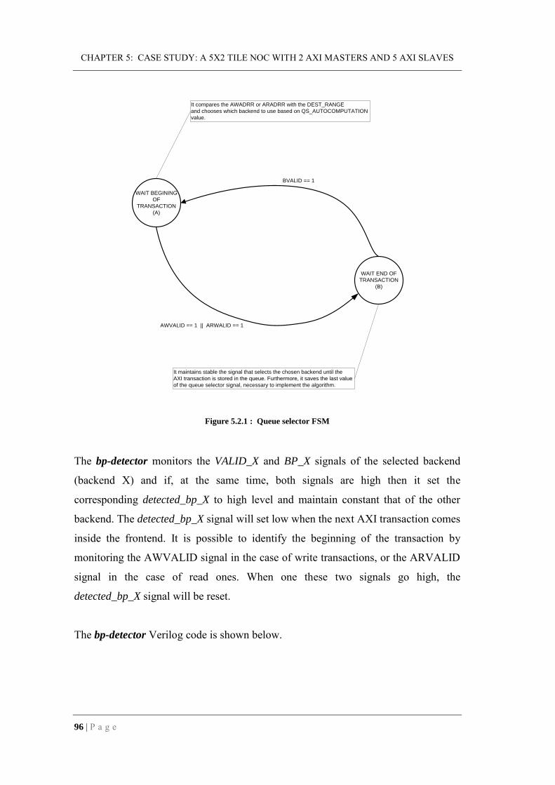
CHAPTER 5: CASE STUDY: A 5X2 TILE NOC WITH 2 AXI MASTERS AND 5 AXI SLAVES
96 | P a g e
Figure 5.2.1 : Queue selector FSM
The bp-detector monitors the VALID_X and BP_X signals of the selected backend
(backend X) and if, at the same time, both signals are high then it set the
corresponding detected_bp_X to high level and maintain constant that of the other
backend. The detected_bp_X signal will set low when the next AXI transaction comes
inside the frontend. It is possible to identify the beginning of the transaction by
monitoring the AWVALID signal in the case of write transactions, or the ARVALID
signal in the case of read ones. When one these two signals go high, the
detected_bp_X signal will be reset.
The bp-detector Verilog code is shown below.
WAIT BEGINING
OF
TRANSACTION
(A)
WAIT END OF
TRANSACTION
(B)
It compares the AWADRR or ARADRR with the DEST_RANGE
and chooses which backend to use based on QS_AUTOCOMPUTATION
value.
It maintains stable the signal that selects the chosen backend until the
AXI transaction is stored in the queue. Furthermore, it saves the last value
of the queue selector signal, necessary to implement the algorithm.
AWVALID == 1 || ARWALID == 1
BVALID == 1

5.2 THE NI SENDER QUEUE SELECTION POLICY
P a g e | 97
Verilog code part 1: Backpressure detector
1: always @(posedge ACLK) 2: begin : bp_detection_update 3: │ if (ARESETn == 1'b0) 4: │ begin 5: │ │ detected_bp_2 <= 1'b0; 6: │ │ detected_bp_1 <= 1'b0; 7: │ │ valid_reg <= 1'b0; 8: │ end 9: │ else 10: │ begin 11: │ │ detected_bp_2 <= detected_bp_next_2; 12: │ │ detected_bp_1 <= detected_bp_next_1; 13: │ │ if (AWVALID == 1'b1 || ARVALID == 1'b1) 14: │ │ valid_reg <= 1'b1; 15: │ │ else 16: │ │ valid_reg <= 1'b0; 17: │ end 18: end 19: 20: always @(VALID_2 || VALID_1 || BP_2 or BP_1 || fend_queue_selector or detected_bp_2 || detected_bp_1) 21: begin: bp_detection 22: │ case (fend_queue_selector) 23: │ │ 2'b10: begin //R2 24: │ │ │ if (VALID_2 == 1'b1 && BP_2 == 1'b1) 25: │ │ │ begin 26: │ │ │ │ detected_bp_next_2 <= 1'b1; 27: │ │ │ │ detected_bp_next_1 <= detected_bp_1; 28: │ │ │ end 29: │ │ │ else 30: │ │ │ begin 31: │ │ │ │ if ((AWVALID == 1'b1 && valid_reg == 1'b0) || (ARVALID == 1'b1 && │ │ │ │ valid_reg == 1'b0)) 32: │ │ │ │ detected_bp_next_1 <= 1'b0; 33: │ │ │ │ else 34: │ │ │ │ detected_bp_next_1 <= detected_bp_1; 35: │ │ │ │ detected_bp_next_2 <= detected_bp_2; 36: │ │ │ end 37: │ │ end 38: │ │ 2'b01: begin //R4 39: │ │ │ if (VALID_1 == 1'b1 && BP_1 == 1'b1) 40: │ │ │ begin 41: │ │ │ │ detected_bp_next_1 <= 1'b1; 42: │ │ │ │ detected_bp_next_2 <= detected_bp_2; 43: │ │ │ end 44: │ │ │ else 45: │ │ │ begin 46: │ │ │ │ if ((AWVALID == 1'b1 && valid_reg == 1'b0) || (ARVALID == 1'b1 && │ │ │ │ valid_reg == 1'b0)) 47: │ │ │ │ detected_bp_next_2 <= 1'b0; 48: │ │ │ │ else 49: │ │ │ │ detected_bp_next_2 <= detected_bp_2; 50: │ │ │ │ detected_bp_next_1 <= detected_bp_1; 51: │ │ │ end 52: │ │ end 53: │ │ default: begin 54: │ │ │ detected_bp_next_1 <= detected_bp_1; 55: │ │ │ detected_bp_next_2 <= detected_bp_2; 56: │ │ end 57: │ endcase 58: end

CHAPTER 5: CASE STUDY: A 5X2 TILE NOC WITH 2 AXI MASTERS AND 5 AXI SLAVES
98 | P a g e
Figure 5.2.2 : Block diagram of the algorithm implementation: at behavioral level (a) and in detail (b)
BP
DETECTOR
QUEUE
SELECTOR
Input signals Input signals
Frontend
parameters
Switch
parametersChosen Switch
BP
DETECTOR
QUEUE
SELECTOR
ARADDR
QS_AUTOCOMPUTATION
mySwitchNum
Detected bp
ARADDR
AWADDR
BP2
BP1
VALID2
VALID1
AWADDR
BVALID
ARVALID
AWVALID
ARESETn
ACLK
detected_bp_2
detected_bp_1
SWITCH_NUM_2
SWITCH_NUM_1
SWITCH_NUM_0
DEST_RANGE_UP
DEST_RANGE_DOWN
fend_queue_selector
Selected backend signal
(a)
(b)

5.3 LATENCY RESULTS
P a g e | 99
5.3 Latency results
I organize the project folder adding 3 sub-folders; Figure 5.3.1 shows this
organization. In the monitors folder there are all the monitor files generated during
the simulation. Latency_computation contains the awk scripts necessary to the end-to-
end latency computation. Instead the gnuplot_graphs folder includes all GNU Plot
scripts that we use for plotting the graphs of end-to-end latency and of the queue
utilization (qu).
Figure 5.3.1 : Project sub-folders
In order to obtain the experimental results we perform the sequence of actions shown
in Figure 5.3.2. At the beginning we erase all monitors in order to make sure that all
previous data are removed.
Then we have to set the parameters for the current simulation. Figure 5.3.3 shows a
summary of simulation parameters.

CHAPTER 5: CASE STUDY: A 5X2 TILE NOC WITH 2 AXI MASTERS AND 5 AXI SLAVES
100 | P a g e
Figure 5.3.2 : Sequence of actions in order to obtain the experimental results
Figure 5.3.3 : Simulation parameters

5.3 LATENCY RESULTS
P a g e | 101
At this point, we can run the simulation and generate the latency results.
We run several simulations in order to explore all the possible configuration of the
NoC in presence of the redundant paths. We used a pseudo-random traffic (prgn)
because it stresses the network more than the other ones (round robin and single
destination – see Section 5.1). The injection data rate at the source is the maximum
possible (the delay parameter corresponds to ―0‖). We distinguish nine different
configurations of the network in terms of alternative path and of selection policy of it
(see Figure 5.3.3).
Figure 5.3.4 and Figure 5.3.5 show the average end-to-end latency from Master 1 and
from Master 2 correspondingly.

CHAPTER 5: CASE STUDY: A 5X2 TILE NOC WITH 2 AXI MASTERS AND 5 AXI SLAVES
102 | P a g e
Figure 5.3.4 : Average end-to-end latency (from Master 1) measured in clock cycle
Figure 5.3.5 : Average end-to-end latency (from Master 2) measured in clock cycle
SL1 SL2 SL3 SL4 SL5
1312
16
20
22
1312
16
19
22
14
11
14
16
18
13
10
14
17
19
1312
16
20
22
13
11
16
18
20
13
11
15
1920
13
11
15
1718
1312
15
18
20
Master 1 @ prgn , delay = (0,0)
Standard Alternative1_rep Alternative2_rep Alternative1+2_rep Alternative1_bp
Alternative2_bp Alternative1+2_bp Alt1_bp+Alt2_rep Alt1_rep+Alt2_bp
SL1 SL2 SL3 SL4 SL5
16
15
12
16
19
15 15
11
14
16
14
11
14
16
18
15
13
12
14
17
16
15
12
15
17
16
14
12
16
19
16
14
12
15
18
16
14
12
16
17
15
14
11
14
16
Master 2 @ prgn , delay = (0,0)
Standard Alternative1_rep Alternative2_rep Alternative1+2_rep Alternative1_bp
Alternative2_bp Alternative1+2_bp Alt1_bp+Alt2_rep Alt1_rep+Alt2_bp

5.3 LATENCY RESULTS
P a g e | 103
We notice that the configuration that gives us the best latency results both for M1 and
M2 is the ―Alternative1+2_rep‖ one. Thus, a repetitive switching, packet-by-packet,
from the standard backend to the alternative one improves the end-to-end latency
better than a switching policy based on the backpressure detection. Looking Figure
5.3.4 and Figure 5.3.5, we can notice that there are some configurations, which could
seem better than the best case earlier chosen. The problem of these configurations is
that they allow the network to obtain this improvement only for packets coming from
one of the two masters; instead for the other one we do not notice the same things.
Figure 5.3.6 shows the best NoC configuration in term of end-to-end average latency.
This configuration allows the NoC to reduce the latency delay of a value near to 10 %
globally. On the other hand, if we analyze each single destination there are cases (see
Figure 5.3.7) where the latency does not improve. Figure 5.3.7 shows the latency
improvement percentage and summarizes all the previous graphs in only one.
Considering this latter figure we understand that the NoC frequency could be reduced
of a value equal to 10% of the actual one, preserving the same performance that is
chieved without alternative paths. In other words, the introduction of redundancy in
the NoC can be used for improving the latency performance and for saving energy.
0
5
10
15
20
SL1 SL2 SL3 SL4 SL5
M2 best case
Standard Alternative1+2_rep
0
5
10
15
20
25
SL1 SL2 SL3 SL4 SL5
M1 best case
Standard Alternative1+2_rep
Figure 5.3.6 : The best NoC configuration in terms of average latency improvement

CHAPTER 5: CASE STUDY: A 5X2 TILE NOC WITH 2 AXI MASTERS AND 5 AXI SLAVES
104 | P a g e
This thesis does not explore (through simulation) the energy aspect, but other works
[10] proved that, using a static multipath routing and reducing the NoC frequency, it
is possible to note an effective energy saving, also in presence of the re-order buffer
at the destination.
Figure 5.3.7 : Percentage of latency improvement
5.4 3-master case
Using the current 2 Masters / 5 Slaves experimental platform, we are managing
average end-to-end values between 10 and 20 clock cycles. The reason for this is that
in such configuration, also in the presence of maximum injected data rate at the
sources, it is impossible to stress the network much more. In fact the NoC is able to
manage the current amount of data traffic, performing such average latency values.
The values shown in Table 5.4.1 are the proof of this consideration. The table shows
0
5
10
15
20
SL1SL2
SL3SL4
SL5
% o
f im
pro
ve
me
nt
Destination
Performance increase
% latency profit M1
% latency profit M2

5.4 3-MASTER CASE
P a g e | 105
the single component latency in the absence of backpressure. Summing the values
together following the path from source to destination we obtain the final end-to-end
latency value. We notice that it is comparable to the average ones of the previous
paragraph. This means that the network is not sufficiently stressed and it can handle
the amount of traffic with a minimal contention of resources.
COMPONENT LATENCY
NI Sender 2x 5
NI Sender 3x 5
Router 1x 2
Router 2x 3
Router 3x 3
Router 4x 3
NI Receiver 1x 2
NI Receiver 2x 3
Table 5.4.1: Latency of NoC components in absence of backpressure
For these reason in this section we analyze another platform, with 3 Master and 5
Slaves, in order to introduce more resource contention inside the NoC and to increase
the latency at the destination. The new AXI Master, named Master 3, is located in
Tile 3. Its introduction involves a sequence of modification, which are listed below:
Introduction of an NI Sender 3x1 and a Router 1x (T3_R3) inside Tile 3;
Modification of the Routers T3_R2, T3_R4, T35_R2 and T2_R3 from 1x to
2x;
Removing of link between T1_R2 and T2_R4.
Figure 5.4.1 shows the new experimental platform.
1 1x = 1 input or 1 output, 2x 2 input or 2 output and so on.

CHAPTER 5: CASE STUDY: A 5X2 TILE NOC WITH 2 AXI MASTERS AND 5 AXI SLAVES
106 | P a g e
Figure 5.4.1 : Experimental platform with one Master more, placed in Tile 3
With one more Master, we have 27 possible configurations of the network, in terms
of source-destination path and alternative path selection policy. In fact we have 3
Master and 3 possible path selection policies (standard path, repetitive switching and
backpressure detection switching). Table 5.4.2 shows all these configurations.
CONFIGURATIONS
MA
STER
SELE
CTI
ON
PO
LIC
Y
Con
fig 1
11
Con
fig 1
12
Con
fig 1
13
Con
fig 1
21
Con
fig 1
22
Con
fig 1
23
Con
fig 1
31
Con
fig 1
32
Con
fig 1
33
Con
fig 2
11
Con
fig 2
12
Con
fig 2
13
Con
fig 2
21
Con
fig 2
22
Con
fig 2
23
Con
fig 2
31
Con
fig 2
32
Con
fig 2
33
Con
fig 3
11
Con
fig 3
12
Con
fig 3
13
Con
fig 3
21
Con
fig 3
22
Con
fig 3
23
Con
fig 3
31
Con
fig 3
32
Con
fig 3
33
M1
Standard x x x x x x x x x
Repetitive x x x x x x x x x
Bp detection x x x x x x x x x
M2
Standard x x x x x x x x x
Repetitive x x x x x x x x x
Bp detection x x x x x x x x x
M3
Standard x x x x x x x x x
Repetitive x x x x x x x x x
Bp detection x x x x x x x x x
Table 5.4.2 : Possible configurations of the experimental platform

5.4 3-MASTER CASE
P a g e | 107
We run the Modelsim RTL simulations for each configuration in order to obtain the
end-to-end latency. The simulation results are summarized in Table 5.4.3: the row
highlighted in red color corresponds to the standard configuration; instead the yellow
row is the best configuration. As in the 2 Masters / 5 Slaves platform, we discard the
configurations that increase the latency with respect to the standard one and we save
the only ones that give us improvements for every destinations. We identified as best
case the configuration 312. This means having the bp detection switching path
section policy for Master 1, the standard path for Master 2 and the repetitive
switching policy for Master 3 (for more details about the selection policy see Section
5.2).
AVERAGE LATENCY
CONFIG. M1 M2 M3
S1 S2 S3 S4 S5 S1 S2 S3 S4 S5 S1 S2 S3 S4 S5
111 16 14 19 25 28 26 24 15 21 23 30 30 22 13 16
112 16 15 20 25 28 26 25 16 22 25 31 30 23 13 14
113 16 15 19 25 27 27 23 15 22 23 31 29 23 13 16
121 16 14 19 25 28 26 25 14 19 19 31 30 22 15 19
122 16 14 19 24 29 26 25 15 18 19 32 31 22 15 15
123 16 14 20 25 28 27 25 14 18 19 32 31 22 15 17
131 16 14 19 24 27 26 25 15 20 21 31 30 22 14 17
132 16 14 19 24 27 26 25 15 20 23 32 30 22 14 15
133 16 14 19 25 27 27 25 15 20 21 31 30 22 14 17
211 16 13 17 20 21 26 22 15 21 24 29 27 22 15 18
212 17 13 17 20 21 26 23 15 21 24 31 29 22 15 15
213 16 13 17 21 21 26 23 15 20 24 30 28 22 15 17
221 16 13 17 21 22 26 23 14 18 20 31 29 21 16 19
222 16 13 17 22 22 26 24 16 20 19 32 29 22 17 15
223 16 13 18 21 23 25 23 15 19 21 30 28 20 16 19
231 16 13 18 21 21 26 24 15 20 21 31 29 22 16 19
232 16 13 17 21 22 26 24 15 21 22 26 24 15 21 22
233 16 13 18 20 22 26 23 15 20 23 30 27 21 16 18
311 16 13 18 22 23 26 24 16 21 24 31 28 22 14 18
312 16 13 18 21 24 25 22 15 20 23 29 26 21 13 15
313 16 13 18 23 25 26 23 16 21 25 31 27 22 14 17
321 16 14 18 22 25 26 23 15 18 20 30 30 22 15 18
322 16 14 18 23 26 26 23 15 19 21 32 30 21 16 17
323 16 13 18 23 24 26 23 16 18 20 30 30 22 16 18
331 16 13 18 22 25 26 23 15 21 22 31 30 21 16 19
332 16 14 18 23 24 26 23 15 20 22 30 29 22 15 16
333 16 13 18 23 24 26 23 15 20 21 31 29 22 15 17
Table 5.4.3 : Average latency value for each configuration of 3 Master / 5 Slaves platform

CHAPTER 5: CASE STUDY: A 5X2 TILE NOC WITH 2 AXI MASTERS AND 5 AXI SLAVES
108 | P a g e
0
5
10
15
20
25
30
s1 s2 s3 s4 s5
LATE
NC
Y
DESTINATION
Best configuration - from M1 111 (standard)
312 (best)
0
5
10
15
20
25
30
s1 s2 s3 s4 s5
LATE
NC
Y
DESTINATION
Best configuration - from M2 111 (standard)
312 (best)
0
5
10
15
20
25
30
s1 s2 s3 s4 s5
LATE
NC
Y
DESTINATION
Best configuration - from M3 111 (standard)
312 (best)
0
5
10
15
20
s1 s2 s3 s4 s5
%
DESTINATION
M1 - Latency improvement [%] benefit [%]
0
2
4
6
8
10
12
14
s1 s2 s3 s4 s5
%
DESTINATION
M3 - Latency improvement [%] benefit [%]
0
2
4
6
8
10
s1 s2 s3 s4 s5
%
DESTINATION
M2 - Latency improvement [%] benefit [%]
(a) (b)
Figure 5.4.2 : Standard vs. best configuration average latency (a), Latency improvement adopting the best
configuration (b)

5.5 SUMMARY
P a g e | 109
More details on the simulation results are presented in the Appendix 2.
5.5 Summary
In this chapter we analyzed a particular case study, that is a 5x2 tile NoC with 2 AXI
Masters and 5 AXI Slaves. Applying the ideas of Section 4.3, we introduced
alternative paths from source to destination. A new version of NI Sender with 3
backend and the logic for the selection of the output queue has been developed. We
distinguish several platform configurations in terms of queue selection policy
(standard / repetitive switching / backpressure detection switching) and alternative
path (used / not used). In Section 5.4 we explored the previous case study, but adding
one additional Master, in order to increase the amount of data traffic in the NoC. The
Master has been placed in Tile 3 and named Master 3.
We compared the latency improvement with the increase of area occupation.
Table 5.5.1 shows a summary of these experimental results. The table considers the
two cases 2M/5S and 3M/5S; for both of them standard and best configuration
(chosen in the previous sections) of the platform are explored.
Using the best configurations, it is possible to improve the end-to-end latency. In the
2M/5S case, the benefit in terms of end-to-end average latency is about 10 %
globally1, but the increase of the total NoC area occupation is about 49 %. In the
other case 3M/5S, the global average latency benefit is near 6 % with an increase of
the total NoC area occupation around 28 %.
The trade-off benefit/drawback is more or less the same; in fact in the first case
(2M/5S) we favor the latency improvement with a resulting big increase of area.
Instead in the other case (3M/5S), we have a small increase of area, but also the
latency benefit is smaller than in the first case.
1 It is the average of ten values. Ten because we have two Masters and five Slaves: M1 to SL1 (1st value), M1 to SL2 (2nd value), and so on.

CHAPTER 5: CASE STUDY: A 5X2 TILE NOC WITH 2 AXI MASTERS AND 5 AXI SLAVES
110 | P a g e
2 MASTER / 5 SLAVES 3 MASTER / 5 SLAVES
STANDARD BEST STANDARD BEST
Average latency
[clock/cycle]
Average
latency
[clock/cycle]
Latency
benefit
[%]
Average latency
[clock/cycle]
Average
latency
[clock/cycle]
Latency
benefit
[%]
MA
ST
ER
1
SLAVE 1 13 13 0 16 16 0 SLAVE 2 12 10 16.67 14 13 7.14 SLAVE 3 16 14 12.50 19 18 5.26 SLAVE 4 20 17 15.00 25 21 16.00 SLAVE 5 22 19 13.64 28 24 14.29
MA
ST
ER
2
SLAVE 1 16 15 6.25 26 25 3.85 SLAVE 2 15 13 13.33 24 22 8.33 SLAVE 3 12 12 0 15 15 0 SLAVE 4 16 14 12.5 21 20 4.76 SLAVE 5 19 17 10.53 23 23 0
MA
ST
ER
3
SLAVE 1 - - - 30 29 3.33 SLAVE 2 - - - 30 26 13.33 SLAVE 3 - - - 22 21 4.56 SLAVE 4 - - - 13 13 0 SLAVE 5 - - - 16 15 6.25
Mean value improvement - - 10 - - 6
STANDARD BEST STANDARD BEST
# of units Area
[µm2] # of units
Area
[µm2] # of units
Area
[µm2] # of units
Area
[µm2]
AR
EA
OC
CU
PA
TIO
N
Router 1x 5 29755 8 47608 3 17853 6 35706
Router 2x 3 33426 5 55710 7 77984 8 89136
NI Sender 2x 2 81620 - - 3 122430 1 40810
NI Sender 3x - - 2 129776 - - 2 129776
NI Receiver 1x 4 68740 2 34370 3 51555 2 34370
NI Receiver 2x 1 34428 3 103284 2 66856 3 100284
Total area [µm2] 247969 370738 336678 430082
Increase [%] - 49.50 - 27.75
Table 5.5.1 : Summary of the latency/area results (standard and best configuration)
The thesis work allowed us to obtain important results, which can be used as starting
point for a fault-tolerant design of the NEC NoC. A simple case of spatial redundancy
has been analyzed with encouraging results.
Since faulty links can have an associated backpressure bit that is kept constantly high,
adopting the backpressure detection switching policy, the NI Sender does not route
packets through those links where the corresponding backpressure bit is high. This
results in a self-repair capability of the network in presence of failures due to delay
variations. In fact, the real bandwidth of some links could be lower than the expected

5.5 SUMMARY
P a g e | 111
ideal value at the designing phase (this due to the technology variation influence).
Therefore a way to use anyway the ―slow links‖ is by monitoring the associated
backpressure bits and when they are congested we change path for a while in order to
guarantee the ideal performance. This it is possible by adopting the ―bp-detection‖
switching policy presented in Section 5.2.
The same NoC link will appear in multiple copies of the same chip. In some of these
chips, the link delay will be acceptable, while in others it will be too high. The
associated backpressure bit will be generated more frequently in the second case and
the ―bp-detection‖ switching policy results in an adaptive routing scheme allowing to
use links according to their available bandwidth.
The result is an adaptive fault-tolerant scheme able to increase the level of yield as a
trade-off with an increase in area and resource utilization.
Actually [7], given a forecasted yield of the 80%, we notice yield loss values near to
25%, considering all parametric variations. Therefore, a fault-tolerant-design
technique is needed in order to sustain an acceptable level of yield. In other words,
fault-tolerant design can allow to produce reliable chips from unreliable components.
This thesis work does not perform failures simulations in order to explore yield
enhancement, but a related work [33] shows that, by adopting method based on the
use of redundant links and crosspoints, it is possible to obtain significant interconnect
yield improvements (up to 72%). Redundant components must be carefully planned
in order to maximize their contribution to the yield increase while keeping acceptable
the area overhead.
This thesis work is just a first step toward the design of fault-tolerant NoCs. The
proposed approach has to be integrated with post-manufacturing diagnostic feedback
for error discovery and localization. Packet reordering is also needed at the
destination and this could be addressed at the application level.

CHAPTER 6: CONCLUSIONS AND FUTURE WORK
112 | P a g e
Chapter 6: Conclusions and future
work
The aim of testing the chips is to detect errors occurred during the fabrication process.
Fault tolerance means the ability for a system to operate in the presence of faults.
There are five key elements to tolerate faults: avoidance, detection, containment,
isolation and recovery. Fault tolerance can be achieved via error detection and
correction, stochastic communication, adaptive routing, and both temporal and spatial
redundancy. Decreasing feature size, higher frequencies, and increased process
variation expose the modern SoC to various faults and countermeasures must be
actively sought and studied.
Even though the NoC concept is still in its infancy in terms of commercial adoption,
it is very actively explored and discussed in the research community. The thesis
analyzed the concept of fault tolerance in relation to the Network on Chip design
paradigm.

P a g e | 113
The NEC Network on Chip was overviewed in order to allow the reader to
understand the explored case study. In Chapter 4 the design of a new version of router
has been also presented.
In Chapter 5 we have explored an example of spatial redundancy solution, which has
been implemented and validated on the NEC NoC. The spatial redundancy was
performed adopting a static multipath routing approach. During the correct operation
of the network, the alternative paths are intelligently employed in order to reduce the
latency and the results of Chapter 5 show that it is possible to obtain clear advantages.
Experimental simulation show that, by adopting the static multipath routing approach,
we can reduce the average end-to-end latency up to the 10 % with a 49.50 % of area
overhead, in the case of 2Masters/5Slaves platform. Instead, in a 3Masters/5Slaves
platform, the latency improvement corresponds to the 6 % with the 27.75 % of area
overhead. Moreover, although we do not perform this evaluation, related work
demonstrates that the adopted approach can reduce the power consumption
maintaining the performances constant.
In presence of faults on one of the two paths (default or alternative) the network is
reconfigured in order to use only the operative one. In this way the end-to-end
communication is ensured.
The latency benefits, obtained by adopting spatial redundancy, allow the network to
use links according to their available bandwidth. If the delay of some links is too high
(due to delay variations) the network can choose another redundant link. This results
in a self-repair capability of the network in presence of failures due to delay
variations. A consequence of these benefits is the increase of the on-chip area due to
the use of redundant alternative paths.
State of the art for NoC has been introduced in order to emphasize the challenges in
this research area. Comparison with buses solutions shows many advantages of the
NoC concept, particularly for huge on-chip systems. Research activities were
presented in order to build an overall picture and show tendencies of the research
community.

CHAPTER 6: CONCLUSIONS AND FUTURE WORK
114 | P a g e
The ideas for future developments of this thesis project are the following:
Re-order buffers:
As logical finalization of the work it is necessary to integrate re-order buffers
in the NoC which permit to order the packets at the destination.
Faults detection:
Another step for continuing this work concerns the possibility to diagnose a
fault. This can be obtained only with the development of a software entity
able to detect faults and set the NoC in order to avoid them.
Routing algorithm modification:
The present routing algorithm used in NEC NoC limits the use of multipath
approaches because it allows packets to turn left or right only once before
reaching their destination. Since it is impossible to ―route around‖ some
faults, without performing two turns, it will be necessary to modify the
routing algorithm in order to allow packets to reach the destination also in the
presence of these faults.

BIBLIOGRAPHY
P a g e | 115
Bibliography
[1] L. Benini, G. De Micheli ―Network on Chip: A new SoC paradigm‖, IEEE
Computer, vol. 35, no 1, pp. 70-78, Jan 2002.
[2] J W. Dally, B. Towles, ―Route Packets, not Wires: On-Chip Interconnection Networks", Proc. DAC, pp. 684-689, June 2001.
[3] J. Williams, ―Digital VLSI Design with Verilog‖, a Textbook from Silicon
Valley Technical Institute, Springer, 2008. [4] http://en.wikipedia.org/wiki/Fault-tolerant_system [5] G. De Micheli, ―On-Chip Networks and Reliable SoC Design", keynote address
of “Diagnostic Services in Network-on-Chips” Workshop in DATE, 2007. [6] M. Lajolo, ―Toward NoC adoption at NEC", in DATE, 2009. [7] M. Lajolo, ―Network on Chip", slides of the intensive Master Course on NoC at
ALaRI Institute (University of Lugano, CH), 2009. [8] D. Ernst, N. S. Kim, S. Pant, S. Das, R. Rao, T. Pham, C. Ziesler, D. Blaauw, T.
Austin, K. Flautner, T. Mudge, ―Razor: A low-power pipeline based on circuit level timing speculation", Proc. of the International Symposium on
Microarchitecture, pp. 7-18, Dec 2003. [9] R. Tamhankar, S. Murali, S. Stergiou, A. Pullini, F. Angiolini, L. Benini, and
G. De Micheli, ``Timing Error Tolerant Network-on-Chip Design Methodology,'' to appear in IEEE Transactions on Computer Aided Design, 2007.
[10] S. Murali, ―Methodologies for reliable and efficient design of Networks on
Chips", Ph.D dissertation, Stanford University, 2007.

BIBLIOGRAPHY
116 | P a g e
[11] J. Hu, R. Marculescu, ―Energy-Aware Mapping for Tile-based NOC Architectures Under Performance Constraints", Proc. ASPDAC, pp. 233-239, Jan 2003.
[12] P. Kundu, ―On Chip interconnects for Tera-scale Processors‖, New
Developments and Trends in Networks on Chip, in DATE, 2009. [13] http://www.necel.com/digital_av/en/mpegdec/emma3sllp.html
[14] http://www.gnuplot.info
[15] http://sourceforge.net/projects/gnuplot
[16] AmbaTM AXI protocol v1.0 specification, http://www.arm.com [17] The IBM CoreConnectTM Bus architecture,
http://www.chips.ibm.com/products/coreconnect [18] Open Core Protocol specification, release 2.1, http://www.ocpip.org [19] R. Locatelli, G. Maruccia, L. Pieralisi, A. Scandura and M. Coppola,
―Spidergon: a novel on-chip communication network‖, Proceedings of
International Symposium on System-on-Chip, 2004. [20] E. Salminen, A. Kulmala and T. D. Hämäläinem, ―Survey of Network-on-Chip
Proposals‖, White paper, OCP-IP, 2008. [21] D. Bertozzi et al., ―NoC synthesis flow for customized domain specific
multiprocessor system-on-chip‖, IEEE Trans. Parallel and Distributed Systems, vol. 16, no 2, pp. 113-129, Feb 2005.
[22] J. Duato, S. Yalamanchili and L. Ni, ―Interconnection networks: An
Engineering Approach‖. Morgan Kaufmann, 2003. [23] W. J. Dally, ―Virtual-channel flow control‖ IEEE Trans. Parallel and
Distributed Systems, vol. 3, no. 2, pp. 194-205, Mar 1992. [24] W. J. Dally and C. L. Seitz, ―Deadlock-free message routing in multiprocessor
interconnection networks‖, IEEE Trans. Compt. 36, pp.547-553, May 1987. [25] J. Bainbridge, and S. Furber, ―CHAIN: A delay-insensitive chip area
interconnect‖, IEEE Micro 22, pp. 16–23, Oct. 2002. [26] T. Bjerregaard and J. Sparsø, ―A router architecture for connectionoriented
service guarantees in the MANGO clockless network-on-chip‖, in Proceedings

BIBLIOGRAPHY
P a g e | 117
of Design, Automation and Testing in Europe Conference (DATE), pp. 1226–
1231, 2005. [27] J. Owens et al., ―Research challenges for on-chip interconnection network‖,
IEEE Micro, vol. 27, no.5, pp. 96–108, 2007. [28] P. Vivet, ―Efficient NoC Design for MPSoC, based on GALS Architecture and
Fine Grain DVFS‖, NoC tutorial, DATE, 2009. [29] S. Vangal et al., ―An 80-tile Sub 100-W TeraFLOPS processor in 65-nm
CMOS‖, IEEE Solid-State Circuits, vol. 43, no. 1, pp. 29-41, Jan 2007. [30] Behavioral Synthesis System Cyber Reference Manual (Rev. 2.6), NEC
internal Document. [31] Seiler, L., Carmean D., Sprangle, E., Forsyth, T., Abrash, M., Dubey, P.,
Junkins, S., Lake, A., Sugerman, J., Cavin, R., Espasa, R., Grochowski, E., Juan, T., Hanrahan, P., 2008. "Larrabee: A Many-Core x86 Architecture for Visual Computing", ACM Transactions on Graphics, 27, 3, 2008.
[32] M.J. Karol et al., ―Input versus output queuing on a space-division packet
switch", in IEEE Transactions on Communications, COM-35(12), pp. 1347-1356, 1987.
[33] Cristian Grecu, André Ivanov, Res Saleh, Partha Pratim Pande, ―NoC
Interconnect Yield Improvement Using Crosspoint Redundancy", in
proceedings of the 21st IEEE International Symposium on Defect and Fault-
Tolerance in VLSI Systems (DFT'06), 2006. [34] http://www.necel.com/cbic/en/core/memory_cb90.html
[35] Gianni. Mereu, ―Conception, analysis, design and realization of a multisocket
network on chip architecture and of the binary translation support for a VLIW core targeted to system on chip", Ph.D dissertation, Cagliari University, 2006.


APPENDIX 1
P a g e | 119
Appendix 1
Architecture diagrams of NEC NoC NIs, Area
occupation data of NoC elements and AXI-NoC
comparison graphs.

APPENDIX 1
120 | P a g e
NI Receiver Architecture (courtesy of NEC Laboratories America Inc.)

APPENDIX 1
P a g e | 121
NI Rdata Sender Architecture (courtesy of NEC Laboratories America Inc.)

APPENDIX 1
122 | P a g e
NI Rdata Receiver Architecture (courtesy of NEC Laboratories America Inc.)

APPENDIX 1
P a g e | 123
courtesy of NEC Laboratories America Inc.
INSTANCE NAME
# LOGIC LEVEL MINIMUM CLOCK
PERIOD[ns] MAXIMUM
FREQUENCY[GHz]
NUMBER OF COMPONENT INSTANCES x PLATFORM
Max. Freq.
400 MHz
1M/5S 2M/5S 3M/5S 8M/8S 16M/16S
AXI_NI_Sender_1x 6 13 0.43 2.325 0 0 0 1 1
AXI_NI_Sender_2x 8 13 0.44 2.272 1 2 3 7 15
AXI_NI_Sender_3x 0 0 0 0 0 0 0 0 0
AXI_NI_Receiver_1x 10 15 0.51 1.96 5 4 3 1 1
AXI_NI_Receiver_2x 12 18 0.57 1.754 0 1 2 7 15
AXI_NI_Receiver_3x 15 19 0.6 1.666 0 0 0 0 0
AXI_NI_Receiver_4x 0 0 0 0 0 0 0 0 0
AXI_NI_Rdata_Sender_1x 8 11 0.42 2.38 5 4 3 1 1
AXI_NI_Rdata_Sender_2x 0 0 0 0 0 1 2 7 15
AXI_NI_Rdata_Sender_3x 0 0 0 0 0 0 0 0 0
AXI_NI_Rdata_Receiver_1x 8 13 0.44 2.272 0 0 0 1 1
AXI_NI_Rdata_Receiver_2x 7 15 0.44 2.272 1 2 3 7 15
AXI_NI_Rdata_Receiver_3x 0 0 0 0 0 0 0 0 0
Router_1x [2 elements] 9 10 0.41 2.439 11 10 9 2 2
Router_2x [2 elements] 9 12 0.43 2.325 3 3 3 16 32
Router_3x [2 elements] 8 11 0.44 2.272 0 2 4 12 28
Router_4x [2 elements] 11 12 0.49 2.04 0 0 0 0 0
Router_1x [4 elements] 8 9 0.43 2.325 11 10 9 2 2
Router_2x [4 elements] 9 12 0.47 2.127 3 3 3 16 32
Router_3x [4 elements] 9 12 0.47 2.127 0 2 4 12 28
Router_4x [4 elements] 10 13 0.53 1.886 0 0 0 0 0

124 | P a g e
APPENDIX 1
courtesy of NEC Laboratories America Inc.
0
0.2
0.4
0.6
0.8
1
1.2
1.4
1.6
1.8
2
1M/5S 2M/5S 3M/5S 8M/8S 16M/16S
Maximum Frequency (GHz)NoC
AXI interconnect (LPI)-Low
AXI interconnect (LPI)- High

APPENDIX 1
P a g e | 125
courtesy of NEC Laboratories America Inc.
1M/5S - MaxFreq
2M/5S - MaxFreq
3M/5S - MaxFreq
8M/5S - MaxFreq
16M/16S - MaxFreq
0
10
20
30
40
50
60
70
80
# of logic levels1M/5S - MaxFreq
1M/5S-400 Mhz
2M/5S - MaxFreq
2M/5S-400 Mhz
3M/5S - MaxFreq
3M/5S-400 Mhz
8M/5S - MaxFreq
8M/5S - 400 Mhz

APPENDIX 1
P a g e | 126
NI Master
total20%
NI Slave total 47%
Routers total [2el]
33%
NoC area composition - 1M/5S @ Max Freq.
Routers with 2-element buffer
NI Master total29%
NI Slave total 41%
Routers total [2el]
30%
NoC area composition - 2M/5S@ Max Freq.
Routers with 2-element buffer
NI Master total34%
NI Slave total 38%
Routers total [2el]
28%
NoC area composition - 3M/5S@ Max Freq.
Routers with 2-element buffer
NI Master total36%
NI Slave total 34%
Routers total [2el]
30%
NoC area composition - 8M/8S@ Max Freq.
Routers with 2-element buffer
NI Master total36%
NI Slave total 34%
Routers total [2el]30%
NoC area composition - 16M/16S@ Max Freq.
Routers with 2-element buffer
NI Master total16%
NI Slave total 40%
Routers total [4el]
44%
NoC area composition - 1M/5S@ Max Freq.
Routers with 4-element buffer
NI Master total24%
NI Slave total 35%
Routers total [4el]
41%
NoC area composition - 2M/5S@ Max Freq.
Routers with 4-element buffer
NI Master total29%
NI Slave total 32%
Routers total [4el]
39%
NoC area composition - 3M/5S@ Max Freq.
Routers with 4-element buffer
NI Master total30%
NI Slave total 29%
Routers total [4el]
41%
NoC area composition - 8M/8S@ Max Freq.
Routers with 4-element buffer
NI Master total30%
NI Slave total 28%
Routers total [4el]
42%
NoC area composition - 16M/16S@ Max Freq.
Routers with 4-element buffer
courtesy of NEC Laboratories America Inc.

APPENDIX 2
P a g e | 127
Appendix 2
5x2 Tiles NoC with 3 AXI Masters / 5 AXI Slaves
experimental platform: latency results for each
NoC configuration and latency graph for single
packet.

P a g e | 128
APPENDIX 2
0
5
10
15
20
25
30
35
111 112 113 121 122 123 131 132 133 211 212 213 221 222 223 231 232 233 311 312 313 321 322 323 331 332 333
LATE
NC
Y [
clo
ck c
ycle
]
CONFIGURATION
End-to-end average Latency of packets coming from Master1
S1 S2 S3 S4 S5

APPENDIX 2
P a g e | 129
0
5
10
15
20
25
30
111 112 113 121 122 123 131 132 133 211 212 213 221 222 223 231 232 233 311 312 313 321 322 323 331 332 333
LATE
NC
Y [
clo
ck c
ycle
]
CONFIGURATION
End-to-end average Latency of packets coming from Master 2
S1 S2 S3 S4 S5

P a g e | 130
APPENDIX 2
0
5
10
15
20
25
30
35
111 112 113 121 122 123 131 132 133 211 212 213 221 222 223 231 232 233 311 312 313 321 322 323 331 332 333
LATE
NC
Y [
clo
ck c
ycle
]
CONFIGURATION
End-to-end average Latency of packets coming from Master3
S1 S2 S3 S4 S5

APPENDIX 2
P a g e | 131
(a) (b)
End-to-end latency from M1, M2, M3 to SLAVE_1 with standard configuration (a) and best configuration (b)

P a g e | 132
APPENDIX 2
(a) (b)
End-to-end latency from M1, M2, M3 to SLAVE_2 with standard configuration (a) and best configuration (b)

APPENDIX 2
P a g e | 133
(a) (b)
End-to-end latency from M1, M2, M3 to SLAVE_3 with standard configuration (a) and best configuration (b)

P a g e | 134
APPENDIX 2
(a) (b)
End-to-end latency from M1, M2, M3 to SLAVE_4 with standard configuration (a) and best configuration (b)
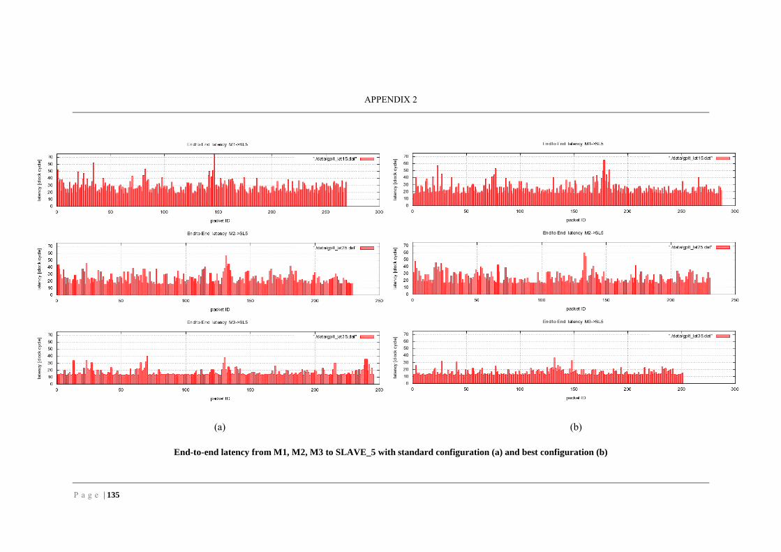
APPENDIX 2
P a g e | 135
(a) (b)
End-to-end latency from M1, M2, M3 to SLAVE_5 with standard configuration (a) and best configuration (b)