fedl610q101-01 ml610q101/ml610q102 lsi is a high-performance 8-bit cmos microcontroller into which...
TRANSCRIPT
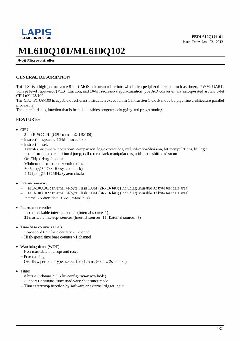
FEDL610Q101-01Issue Date: Jan. 23, 2013
ML610Q101/ML610Q102 8-bit Microcontroller
1/21
GENERAL DESCRIPTION This LSI is a high-performance 8-bit CMOS microcontroller into which rich peripheral circuits, such as timers, PWM, UART, voltage level supervisor (VLS) function, and 10-bit successive approximation type A/D converter, are incorporated around 8-bit CPU nX-U8/100. The CPU nX-U8/100 is capable of efficient instruction execution in 1-intruction 1-clock mode by pipe line architecture parallel processing. The on-chip debug function that is installed enables program debugging and programming. FEATURES • CPU
− 8-bit RISC CPU (CPU name: nX-U8/100) − Instruction system: 16-bit instructions − Instruction set:
Transfer, arithmetic operations, comparison, logic operations, multiplication/division, bit manipulations, bit logic operations, jump, conditional jump, call return stack manipulations, arithmetic shift, and so on
− On-Chip debug function − Minimum instruction execution time
30.5μs (@32.768kHz system clock) 0.122μs (@8.192MHz system clock)
• Internal memory
− ML610Q101 : Internal 4Kbyte Flash ROM (2K×16 bits) (including unusable 32 byte test data area) − ML610Q102 : Internal 6Kbyte Flash ROM (3K×16 bits) (including unusable 32 byte test data area) − Internal 256byte data RAM (256×8 bits)
• Interrupt controller
− 1 non-maskable interrupt source (Internal source: 1) − 21 maskable interrupt sources (Internal sources: 16, External sources: 5)
• Time base counter (TBC)
− Low-speed time base counter ×1 channel − High-speed time base counter ×1 channel
• Watchdog timer (WDT)
− Non-maskable interrupt and reset − Free running − Overflow period: 4 types selectable (125ms, 500ms, 2s, and 8s)
• Timer
− 8 bits × 6 channels (16-bit configuration available) − Support Continuos timer mode/one shot timer mode − Timer start/stop function by software or external trigger input

FEDL610Q101 -01
ML610Q101/ML610Q102
2/21
• PWM
− Resolution 16 bits × 1 channel − Support Continuos timer mode/one shot timer mode − PWM start/stop function by software or external trigger input
• UART
− Half-duplex − TXD/RXD × 1 channels − Bit length, parity/no parity, odd parity/even parity, 1 stop bit/2 stop bits − Positive logic/negative logic selectable − Built-in baud rate generator
• Successive approximation type A/D converter (SA-ADC)
− 10-bit A/D converter − Input × 6 channels
• Analog Comparator
− Operating voltage: VDD = 2.7V to 5.5V − Input voltage by common mode: VDD = 0.1V to VDD - 1.5V − Hysteresis (Comparator0 only): 20mV(Typ.) − Allows selection of interrupt disabled mode,falling-edge interrupt mode,rising-edge interrupt mode,
or both-edge interrupt mode. • General-purpose ports (GPIO)
− Input/output port × 11 channels (including secondary functions)
• Reset − Reset by the RESET_N pin − Reset by power-on detection − Reset by the watchdog timer (WDT) overflow − Reset by voltage level supervisor(VLS)
• Voltage level supervisor(VLS) − Judgment accuracy: ±3.0% (Typ.) − It can be used for low level detection reset.
• Clock − Low-speed clock:
Built-in RC oscillation (32.768 kHz) − High-speed clock:
Built-in PLL oscillation (16.384 MHz), external clock The clock of the CPU is 8.192MHz(Max)
− Selection of high-speed clock mode by software: Built-in PLL oscillation, external clock
• Power management
− HALT mode: Instruction execution by CPU is suspended (peripheral circuits are in operating states). − STOP mode: Stop of low-speed oscillation and high-speed oscillation (Operations of CPU and peripheral circuits are
stopped.) − Clock gear: The frequency of high-speed system clock can be changed by software (1/1, 1/2, 1/4, or 1/8 of the oscillation
clock) − Block Control Function: Power down (reset registers and stop clock supply) the circuits of unused peripherals.

FEDL610Q101 -01
ML610Q101/ML610Q102
3/21
• Shipment
− 16-pin plastic SSOP ML610Q101-xxxMB (Blank product: ML610Q101-NNNMB) ML610Q102-xxxMB (Blank product: ML610Q102-NNNMB)
• Guaranteed operating range
− Operating temperature: −40°C to 85°C − Operating voltage: VDD = 2.7V to 5.5V
FEDL610Q101 -01
ML610Q101/ML610Q102
4/21
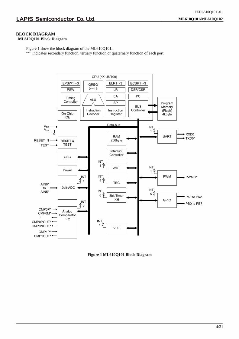
BLOCK DIAGRAM ML610Q101 Block Diagram
Figure 1 show the block diagram of the ML610Q101. "*" indicates secondary function, tertiary function or quaternary function of each port.
Figure 1 ML610Q101 Block Diagram
Program Memory (Flash) 4kbyte
UART RXD0 TXD0*
INT1
RAM 256byte
Interrupt Controller
CPU (nX-U8/100)
Timing Controller
EA
SP
On-Chip ICE
InstructionDecoder
BUS ControllerInstruction
Register
TBC
INT4
INT1
WDT
INT6 8bit Timer
×6
INT1
PWM
GPIO
PA0 to PA2
INT5
PB0 to PB7
Data-bus
PWMC*
TEST RESET_N
OSC
Power
RESET & TEST
ALU
EPSW1~3
PSW
ELR1~3
LR
ECSR1~3
DSR/CSR
PC
GREG 0~15
VDD VSS
Analog Comparator
×2
CMP0P* CMP0M*
INT 2
10bit-ADC AIN0*
to AIN5*
INT 1
VLS
1
CMP1OUT* CMP1P*
CMP0POUT*CMP0NOUT*
INT1
FEDL610Q101 -01
ML610Q101/ML610Q102
5/21
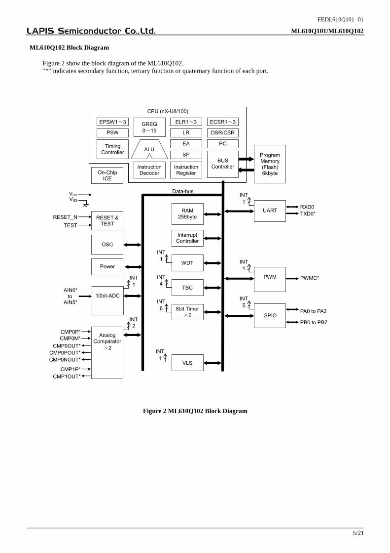
ML610Q102 Block Diagram
Figure 2 show the block diagram of the ML610Q102. "*" indicates secondary function, tertiary function or quaternary function of each port.
Figure 2 ML610Q102 Block Diagram
Program Memory (Flash) 6kbyte
UART RXD0 TXD0*
INT1
RAM 256byte
Interrupt Controller
CPU (nX-U8/100)
Timing Controller
EA
SP
On-Chip ICE
InstructionDecoder
BUS ControllerInstruction
Register
TBC
INT4
INT1
WDT
INT6 8bit Timer
×6
INT1
PWM
GPIO
PA0 to PA2
INT5
PB0 to PB7
Data-bus
PWMC*
TEST RESET_N
OSC
Power
RESET &TEST
ALU
EPSW1~3
PSW
ELR1~3
LR
ECSR1~3
DSR/CSR
PC
GREG 0~15
VDD VSS
Analog Comparator
×2
CMP0P* CMP0M*
INT 2
10bit-ADCAIN0*
to AIN5*
INT 1
VLS
CMP0OUT*
CMP1OUT* CMP1P*
CMP0POUT*CMP0NOUT*
INT1

FEDL610Q101 -01
ML610Q101/ML610Q102
6/21
PIN CONFIGURATION
ML610Q101/ML610Q102 SSOP16 Pin Layout Figure 3 show the SSOP16 pin layout of the ML610Q101/ML610Q102.
Figure 3 ML610Q101/ML610Q102 SSOP16 Pin Configuration
RESET_N TEST
PB0 / PWMC / OUTCLK / CMP1OUT PB1 / TXD0
PB2 / CMP0POUT PB3 / CMP0MOUT
PA2 / CLKIN / CMP0OUT VPP
12345678
PA0 / PWMC / OUTCLK / TM9OUTPB7 / LSCLK / PWMC VDD VSS
PB6 / CLKIN PB5 / PB4 / TXD0 PA1 / LSCLK / TMFOUT
161514131211109
FEDL610Q101 -01
ML610Q101/ML610Q102
7/21
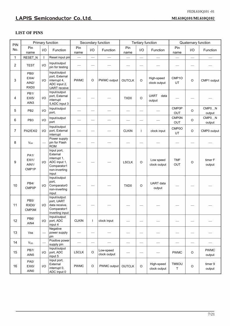
LIST OF PINS
Primary function Secondary function Tertiary function Quaternary function PIN No. Pin
name I/O Function
Pin name
I/O Function Pin
name I/O Function
Pin name
I/O Function
1 RESET_N I Reset input pin ⎯ ⎯ ⎯ ⎯ ⎯ ⎯ ⎯ ⎯ ⎯
2 TEST I/O Input/output pin for testing ⎯ ⎯ ⎯ ⎯ ⎯ ⎯ ⎯ ⎯ ⎯
3
PB0/ EXI4/ AIN2/ RXD0
I/O
Input/output port, External interrupt 4, ADC input 2, UART receive
PWMC O PWMC output OUTCLK O High-speed clock output
CMP1OUT
O CMP1 output
4 PB1/ EXI5/ AIN3
I/O
Input/output port, External interrupt 5,ADC input 3
⎯ ⎯ ⎯ TXD0 O UART data output
⎯ ⎯ ⎯
5 PB2 I/O Input/output port, ⎯ ⎯ ⎯ ⎯ ⎯ ⎯
CMP0POUT
O CMP0_N
output
6 PB3 I/O Input/output port ⎯ ⎯ ⎯ ⎯ ⎯ ⎯
CMP0NOUT
O CMP0_N
output
7 PA2/EXI2 I/O Input/output port, External interrupt
⎯ ⎯ ⎯ CLKIN I clock input CMP0O
UT O CMP0 output
8 VPP ⎯ Power supply pin for Flash ROM
⎯ ⎯ ⎯ ⎯ ⎯ ⎯ ⎯ ⎯ ⎯
9
PA1/ EXI1/ AIN1/
CMP1P
I/O
Input port, External interrupt 1, ADC input 1, Comparator1 non-inverting input
⎯ ⎯ ⎯ LSCLK O Low speed clock output
TMF OUT
O timer F output
10 PB4/
CMP0P I/O
Input/output port, Comparator0 non-inverting input
⎯ ⎯ ⎯ TXD0 O UART data
output ⎯ ⎯ ⎯
11 PB5/
RXD0/ CMP0M
I/O
Input/output port, UART data receive, Comparator1 inverting input
⎯ ⎯ ⎯ ⎯ ⎯ ⎯ ⎯ ⎯ ⎯
12 PB6/ AIN4
I/O Input/output port, ADC input 4
CLKIN I clock input ⎯ ⎯ ⎯ ⎯ ⎯ ⎯
13 Vss ⎯ Negative power supply pin
⎯ ⎯ ⎯ ⎯ ⎯ ⎯ ⎯ ⎯ ⎯
14 VDD ⎯ Positive power supply pin ⎯ ⎯ ⎯ ⎯ ⎯ ⎯ ⎯ ⎯ ⎯
15 PB7/ AIN5
I/O Input/output port, ADC input 5
LSCLK O Low-speed clock output ⎯ ⎯ ⎯ PWMC O
PWMC output
16 PA0/ EXI0/ AIN0
I/O
Input port, External interrupt 0, ADC input 0
PWMC O PWMC output OUTCLK O High-speed clock output
TM9OUT
O timer 9 output
FEDL610Q101 -01
ML610Q101/ML610Q102
8/21
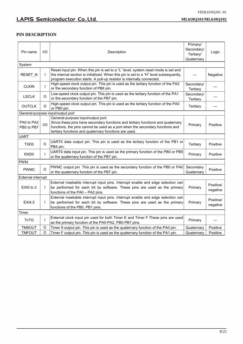
PIN DESCRIPTION
Pin name I/O Description
Primary/ Secondary/
Tertiary/ Quaternary
Logic
System
RESET_N I Reset input pin. When this pin is set to a “L” level, system reset mode is set and the internal section is initialized. When this pin is set to a “H” level subsequently, program execution starts. A pull-up resistor is internally connected.
— Negative
CLKIN I High-speed clock output pin. This pin is used as the tertiary function of the PA2 or the secondary function of PB6 pin.
Secondary/Tertiary
—
LSCLK O Low-speed clock output pin. This pin is used as the tertiary function of the PA1 or the secondary function of the PB7 pin.
Secondary/Tertiary —
OUTCLK O High-speed clock output pin. This pin is used as the tertiary function of the PA0 or PB0 pin. Tertiary —
General-purpose input/output port
PA0 to PA2 PB0 to PB7
I/O
General-purpose input/output port. Since these pins have secondary functions and tertiary functions and quaternary functions, the pins cannot be used as a port when the secondary functions and tertiary functions and quaternary functions are used.
Primary Positive
UART
TXD0 O UART0 data output pin. This pin is used as the tertiary function of the PB1 or PB4 pin.
Tertiary Positive
RXD0 I UART0 data input pin. This pin is used as the primary function of the PB0 or PB5 or the quaternary function of the PB7 pin.
Primary Positive
PWM
PWMC O PWMC output pin. This pin is used as the secondary function of the PB0 or PA0 or the quaternary function of the PB7 pin.
SecondaryQuaternary
Positive
External interrupt
EXI0 to 2 I External maskable interrupt input pins. Interrupt enable and edge selection can be performed for each bit by software. These pins are used as the primary functions of the PA0 – PA2 pins.
Primary Positive/negative
EXI4,5 I External maskable interrupt input pins. Interrupt enable and edge selection can be performed for each bit by software. These pins are used as the primary functions of the PB0, PB1 pins.
Primary Positive/negative
Timer
TnTG I External clock input pin used for both Timer E and Timer F.These pins are used as the primary function of the PA0-PA2, PB0-PB7 pins.
Primary —
TM9OUT O Timer 9 output pin. This pin is used as the quaternary function of the PA0 pin. Quaternary PositiveTMFOUT O Timer F output pin. This pin is used as the quaternary function of the PA1 pin. Quaternary Positive
FEDL610Q101 -01
ML610Q101/ML610Q102
9/21
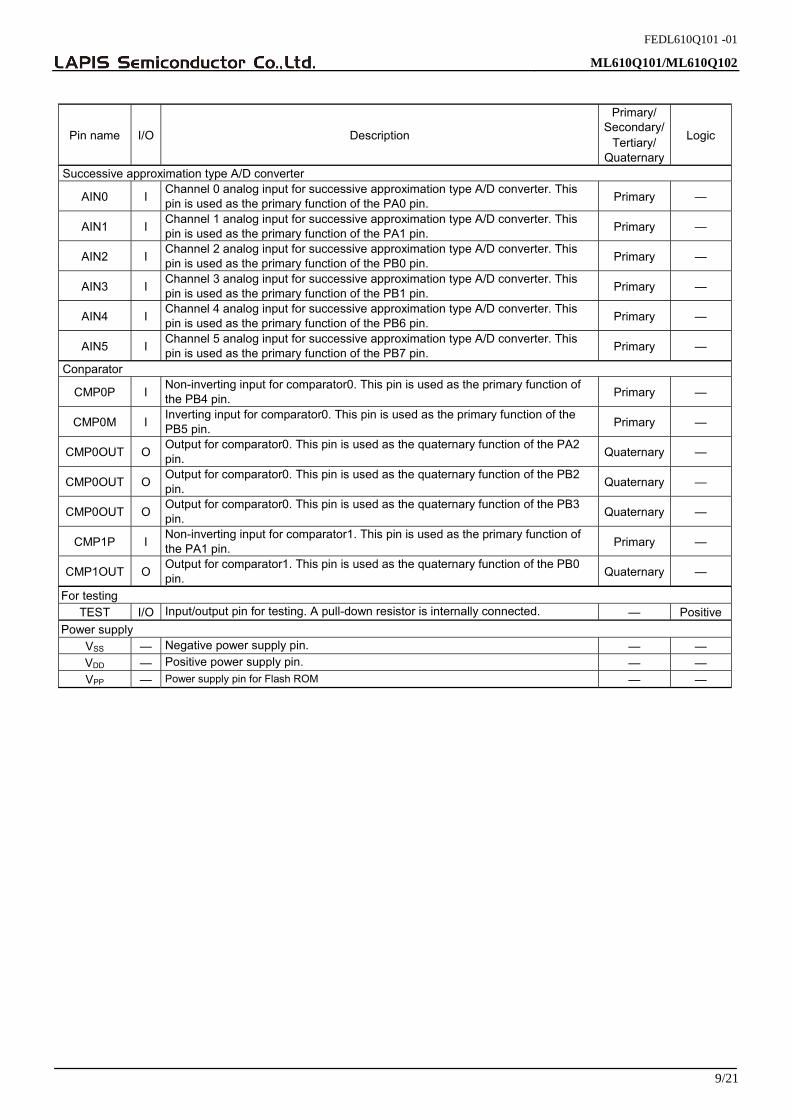
Pin name I/O Description
Primary/ Secondary/
Tertiary/ Quaternary
Logic
Successive approximation type A/D converter
AIN0 I Channel 0 analog input for successive approximation type A/D converter. This pin is used as the primary function of the PA0 pin. Primary —
AIN1 I Channel 1 analog input for successive approximation type A/D converter. This pin is used as the primary function of the PA1 pin. Primary —
AIN2 I Channel 2 analog input for successive approximation type A/D converter. This pin is used as the primary function of the PB0 pin. Primary —
AIN3 I Channel 3 analog input for successive approximation type A/D converter. This pin is used as the primary function of the PB1 pin. Primary —
AIN4 I Channel 4 analog input for successive approximation type A/D converter. This pin is used as the primary function of the PB6 pin. Primary —
AIN5 I Channel 5 analog input for successive approximation type A/D converter. This pin is used as the primary function of the PB7 pin. Primary —
Conparator
CMP0P I Non-inverting input for comparator0. This pin is used as the primary function of the PB4 pin. Primary —
CMP0M I Inverting input for comparator0. This pin is used as the primary function of the PB5 pin. Primary —
CMP0OUT O Output for comparator0. This pin is used as the quaternary function of the PA2 pin. Quaternary —
CMP0OUT O Output for comparator0. This pin is used as the quaternary function of the PB2 pin. Quaternary —
CMP0OUT O Output for comparator0. This pin is used as the quaternary function of the PB3 pin. Quaternary —
CMP1P I Non-inverting input for comparator1. This pin is used as the primary function of the PA1 pin. Primary —
CMP1OUT O Output for comparator1. This pin is used as the quaternary function of the PB0 pin. Quaternary —
For testing TEST I/O Input/output pin for testing. A pull-down resistor is internally connected. — Positive
Power supply VSS — Negative power supply pin. — — VDD — Positive power supply pin. — — VPP — Power supply pin for Flash ROM — —
FEDL610Q101 -01
ML610Q101/ML610Q102
10/21
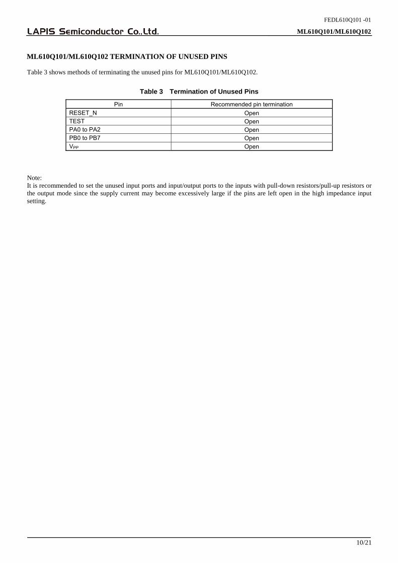
ML610Q101/ML610Q102 TERMINATION OF UNUSED PINS Table 3 shows methods of terminating the unused pins for ML610Q101/ML610Q102.
Table 3 Termination of Unused Pins
Pin Recommended pin termination RESET_N Open TEST Open PA0 to PA2 Open PB0 to PB7 Open VPP Open
Note: It is recommended to set the unused input ports and input/output ports to the inputs with pull-down resistors/pull-up resistors or the output mode since the supply current may become excessively large if the pins are left open in the high impedance input setting.
FEDL610Q101 -01
ML610Q101/ML610Q102
11/21
ELECTRICAL CHARACTERISTICS
ABSOLUTE MAXIMUM RATINGS (VSS = 0V)
Parameter Symbol Condition Rating Unit
Power supply voltage 1 VDD Ta = 25°C −0.3 to +7.0 V Power supply voltage 2 VPP Ta = 25°C −0.3 to +9.5 V Input voltage VIN Ta = 25°C −0.3 to VDD+0.3 V Output voltage VOUT Ta = 25°C −0.3 to VDD+0.3 V Output current 1 IOUT1 Ta = 25°C −12 to +11 mA Power dissipation PD Ta = 25°C 0.5 mW Storage temperature TSTG ⎯ −55 to +150 °C
RECOMMENDED OPERATING CONDITIONS
(VSS = 0V)
Parameter Symbol Condition Range Unit
Operating temperature TOP ⎯ −40 to +85 °C
Operating voltage VDD ⎯ 2.7 to 5.5 V
Operating frequency (CPU) fOP VDD = 2.7V to 5.5V 30k to 8.4M Hz
OPERATING CONDITIONS OF FLASH MEMORY (VSS=0V)
Rating Parameter Symbol Condition Min. Typ. Max.
Unit
Operating temperature TOP At write/erase 0 ― +40 °C VDD At write/erase 4.5 ― 5.5 V Operating voltage VPP At write/erase 7.7 ― 8.3
Rewrite counts CEP ― ― ― 80 cycles Data retention*1 YDR ― 10 ― ― years *1 : However, please keep active time of the flash memory from exceeding ten years. Vpp pin has internal pull-down resistor.
FEDL610Q101 -01
ML610Q101/ML610Q102
12/21
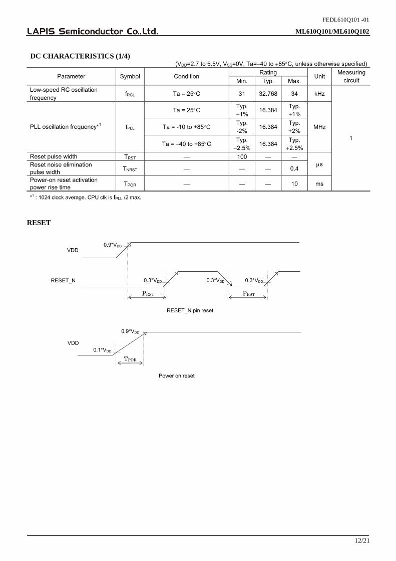
DC CHARACTERISTICS (1/4)
(VDD=2.7 to 5.5V, VSS=0V, Ta=−40 to +85°C, unless otherwise specified)Rating
Parameter Symbol Condition Min. Typ. Max.
Unit Measuring
circuit Low-speed RC oscillation frequency
fRCL Ta = 25°C 31 32.768 34 kHz
Ta = 25°C Typ. −1%
16.384Typ. +1%
Ta = -10 to +85°C Typ. -2%
16.384Typ. +2%
PLL oscillation frequency*1 fPLL
Ta = −40 to +85°C Typ.
−2.5%16.384
Typ. +2.5%
MHz
Reset pulse width TRST ⎯ 100 ― ― Reset noise elimination pulse width TNRST ⎯ ― ― 0.4
μs
Power-on reset activation power rise time TPOR ⎯ ― ― 10 ms
1
*1 : 1024 clock average. CPU clk is fPLL /2 max.
RESET
PRST
RESET_N
RESET_N pin reset
VDD 0.9*VDD
0.3*VDD
VDD
0.9*VDD
0.1*VDD
TPOR
Power on reset
PRST
0.3*VDD0.3*VDD

FEDL610Q101 -01
ML610Q101/ML610Q102
13/21
DC CHARACTERISTICS (2/4)
(VDD=2.7 to 5.5V, VSS=0V, Ta=−40 to +85°C, unless otherwise specified)Rating
Parameter Symbol Condition Min. Typ. Max.
Unit Measuring
circuit
Ta=25°C , VDD=fall Typ −3.0%
2.85 Typ +3.0% VVLS0F
VDD=fall Typ.−5.0%
2.85 Typ. +5.0%
Ta=25°C , VDD=rise Typ.−3.0%
2.92 Typ. +3.0%
VVLS0R
VDD=rise Typ.−5.0%
2.92 Typ. +5.0%
VLS0=0 3.295Ta=25°C
VLS0=1
Typ −3.0% 3.625
Typ +3.0%
VLS0=0 3.295
VLS Judgment voltage
VVLS1
― VLS0=1
Typ −5.0% 3.625
Typ +5.0%
V 1
Comparator0 In-phase input voltage range
VCMR ― 0.1 ― VDD -1.5
V
Ta=25°C , VDD = 5.0V 10 20 30 Comparator0 hysteresis VHYSP
VDD = 5.0V 5 20 35 Comparator0 Input offset voltage
VCMOF Ta=25°C , VDD = 5.0V ― ― 7
Ta=25°C -25 ― 25 Comparator Reference- voltage error*3
VCMREF ― -50 ― 50
mV
4
Supply current 1 IDD1 CPU: In STOP state. Low-speed/high-speed oscillation: stopped.
Ta=-40 to +85°C ― 1 30 μA
Supply current 2 IDD2
CPU: In 32.768kHz operating state.*1
High-speed oscillation: Stopped.
Ta=-40 to +85°C ― 3.7 6 mA
1
*1 : LTBC and WDT are operating ,and significant bits of BLKCON0 to BLKCON4 registers are all “1”. *2 : When the CPU operating rate is 100%. Minimum instruction execution time: Approx 0.122 μs (at 8.192MHz system clock) *3 :Comparator input offset voltage is included.
FEDL610Q101 -01
ML610Q101/ML610Q102
14/21
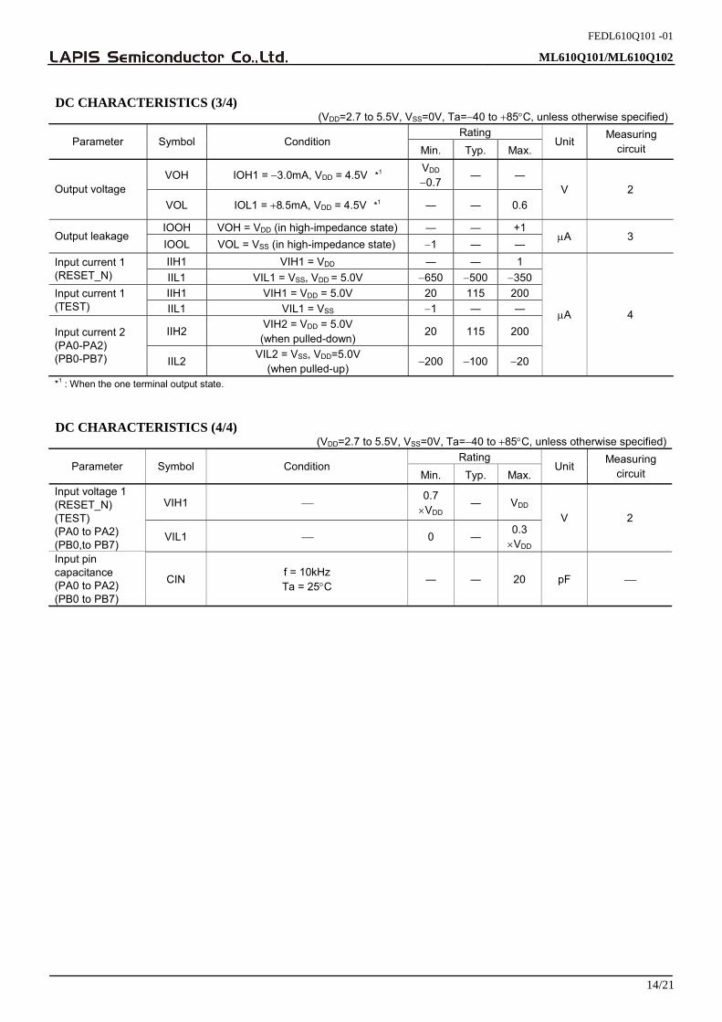
DC CHARACTERISTICS (3/4)
(VDD=2.7 to 5.5V, VSS=0V, Ta=−40 to +85°C, unless otherwise specified) Rating
Parameter Symbol Condition Min. Typ. Max.
Unit Measuring
circuit
VOH IOH1 = −3.0mA, VDD = 4.5V *1 VDD
−0.7 ― ―
Output voltage VOL IOL1 = +8.5mA, VDD = 4.5V *1 ― ― 0.6
V 2
IOOH VOH = VDD (in high-impedance state) ― ― +1 Output leakage
IOOL VOL = VSS (in high-impedance state) −1 ― ― μA 3
IIH1 VIH1 = VDD ― ― 1 Input current 1 (RESET_N) IIL1 VIL1 = VSS, VDD = 5.0V −650 −500 −350
IIH1 VIH1 = VDD = 5.0V 20 115 200 Input current 1 (TEST) IIL1 VIL1 = VSS −1 ― ―
IIH2 VIH2 = VDD = 5.0V (when pulled-down)
20 115 200 Input current 2 (PA0-PA2) (PB0-PB7) IIL2
VIL2 = VSS, VDD=5.0V
(when pulled-up) −200 −100 −20
μA 4
*1 : When the one terminal output state. DC CHARACTERISTICS (4/4)
(VDD=2.7 to 5.5V, VSS=0V, Ta=−40 to +85°C, unless otherwise specified) Rating
Parameter Symbol Condition Min. Typ. Max.
Unit Measuring
circuit
VIH1 ⎯ 0.7
×VDD ― VDD
Input voltage 1 (RESET_N) (TEST) (PA0 to PA2) (PB0,to PB7)
VIL1 ⎯ 0 ― 0.3
×VDD
V 2
Input pin capacitance (PA0 to PA2) (PB0 to PB7)
CIN f = 10kHz Ta = 25°C
― ― 20 pF ⎯
FEDL610Q101 -01
ML610Q101/ML610Q102
15/21
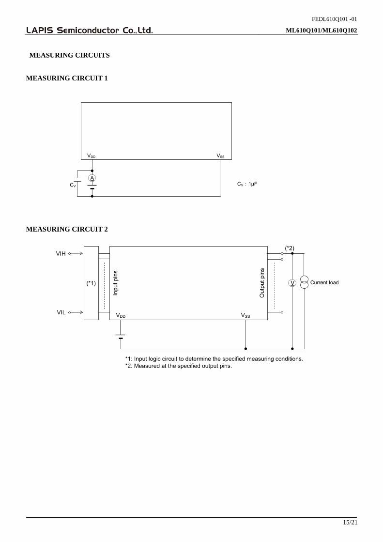
MEASURING CIRCUITS
MEASURING CIRCUIT 1
MEASURING CIRCUIT 2
A
VDD VSS
CV:1μF
CV
Inpu
t pin
s
VDD VSS
VIH
VIL
Out
put p
ins
*1: Input logic circuit to determine the specified measuring conditions. *2: Measured at the specified output pins.
(*2)
(*1) Current loadV

FEDL610Q101 -01
ML610Q101/ML610Q102
16/21
MEASURING CIRCUIT 3 MEASURING CIRCUIT 4
Inpu
t pin
s
A
VDD VSS
Out
put p
ins
*3: Measured at the specified output pins.
(*3)
Inpu
t pin
s
A
VDD VSS
VIH
VIL
Out
put p
ins
*1: Input logic circuit to determine the specified measuring conditions. *2: Measured at the specified output pins.
(*2)
(*1)

FEDL610Q101 -01
ML610Q101/ML610Q102
17/21
AC CHARACTERISTICS (External Interrupt)
(VDD=2.7 to 5.5V, VSS=0V, Ta=−40 to +85°C, unless otherwise specified)Rating
Parameter Symbol Condition Min. Typ. Max.
Unit
External interrupt disable period TNUL Interrupt: Enabled (MIE = 1),
CPU: NOP operation System clock: 32.768kHz
2.5 x sysclk
― 3.5 x sysclk
μs
tNUL
PA0 to PA2, PB0 to PB1
(Rising-edge interrupt)
(Falling-edge interrupt)
P00 ,P01,PB0 – PB2
(Both-edge interrupt) tNUL
tNUL
PA0 to PA2, PB0 to PB1
PA0 to PA2, PB0 to PB1

FEDL610Q101 -01
ML610Q101/ML610Q102
18/21
Electrical Characteristics of Successive Approximation Type A/D Converter
(VDD=2.7 to 5.5V, VSS=0V, Ta=−40 to +85°C, unless otherwise specified)Rating
Parameter Symbol Condition Min. Typ. Max.
Unit
Resolution n ⎯ ― ― 10 bit Integral non-linearity error INL RI≦5kΩ, HSCLK=8.192MHz −4 ― +4 Differential non-linearity error DNL RI≦5kΩ, HSCLK=8.192MHz −3 ― +3 Zero-scale error VOFF RI≦5kΩ, HSCLK=8.192MHz −4 ― +4 Full-scale error FSE RI≦5kΩ, HSCLK=8.192MHz −4 ― +4
LSB
Conversion time tCONV ⎯ ― 102 ― φ/CHφ: fPLL/4
A
VDD
VSSAnalog input
− RI≤5kΩ AIN0 to AIN7
0.1μF
+ 10μF

FEDL610Q101 -01
ML610Q101/ML610Q102
19/21
PACKAGE DIMENSIONS
(Unit: mm)
Notes for Mounting the Surface Mount Type Package The surface mount type packages are very susceptible to heat in reflow mounting and humidity absorbed in storage. Therefore, before you perform reflow mounting, contact ROHM’s responsible sales person for the product name, package name, pin number, package code and desired mounting conditions (reflow method, temperature and times).

FEDL610Q101 -01
ML610Q101/ML610Q102
20/21
REVISION HISTORY
Page Document No. Date Previous
Edition CurrentEdition
Description
FEDL610Q101-1 Jan,23,2013 – – Final edition 1
FEDL610Q101 -01
ML610Q101/ML610Q102
21/21
NOTES No copying or reproduction of this document, in part or in whole, is permitted without the consent of LAPIS Semiconductor Co., Ltd. The content specified herein is subject to change for improvement without notice. The content specified herein is for the purpose of introducing LAPIS Semiconductor's products (hereinafter "Products"). If you wish to use any such Product, please be sure to refer to the specifications, which can be obtained from LAPIS Semiconductor upon request. Examples of application circuits, circuit constants and any other information contained herein illustrate the standard usage and operations of the Products. The peripheral conditions must be taken into account when designing circuits for mass production. Great care was taken in ensuring the accuracy of the information specified in this document. However, should you incur any damage arising from any inaccuracy or misprint of such information, LAPIS Semiconductor shall bear no responsibility for such damage. The technical information specified herein is intended only to show the typical functions of and examples of application circuits for the Products. LAPIS Semiconductor does not grant you, explicitly or implicitly, any license to use or exercise intellectual property or other rights held by LAPIS Semiconductor and other parties. LAPIS Semiconductor shall bear no responsibility whatsoever for any dispute arising from the use of such technical information. The Products specified in this document are intended to be used with general-use electronic equipment or devices (such as audio visual equipment, office-automation equipment, communication devices, electronic appliances and amusement devices). The Products specified in this document are not designed to be radiation tolerant. While LAPIS Semiconductor always makes efforts to enhance the quality and reliability of its Products, a Product may fail or malfunction for a variety of reasons. Please be sure to implement in your equipment using the Products safety measures to guard against the possibility of physical injury, fire or any other damage caused in the event of the failure of any Product, such as derating, redundancy, fire control and fail-safe designs. LAPIS Semiconductor shall bear no responsibility whatsoever for your use of any Product outside of the prescribed scope or not in accordance with the instruction manual. The Products are not designed or manufactured to be used with any equipment, device or system which requires an extremely high level of reliability the failure or malfunction of which may result in a direct threat to human life or create a risk of human injury (such as a medical instrument, transportation equipment, aerospace machinery, nuclear-reactor controller, fuel-controller or other safety device). LAPIS Semiconductor shall bear no responsibility in any way for use of any of the Products for the above special purposes. If a Product is intended to be used for any such special purpose, please contact a ROHM sales representative before purchasing. If you intend to export or ship overseas any Product or technology specified herein that may be controlled under the Foreign Exchange and the Foreign Trade Law, you will be required to obtain a license or permit under the Law.
Copyright 2013 LAPIS Semiconductor Co., Ltd.

Mouser Electronics
Authorized Distributor
Click to View Pricing, Inventory, Delivery & Lifecycle Information: ROHM Semiconductor:
ML610Q101-NNNMBZ0ATL ML610Q102-NNNMBZ0ATL ML610Q101-NNNGDZ0ANL ML610Q102-NNNGDZ0ANL
ML610Q102 reference board