fedl7074-004-01 ml7074-004 - lapis-semi. · pdf filevoip codec 1/98 general description ......
TRANSCRIPT

FEDL7074-004-01Issue Date: Nov. 12, 2003
ML7074-004 VoIP CODEC
1/98
GENERAL DESCRIPTION The ML7074-004 is a speech CODEC for VoIP. This LSI allows selection of G.729.A, or G.711 standard as a speech CODEC. The LSI is optimum for adding VoIP functions to TAs, routers, etc., since it has the functions of an echo canceller for 32 ms delay, DTMF detection, tone detection, tone generation, etc. FEATURES Single 3.3 V power supply operation (DVDD0, 1, 2, AVDD: 3.0 to 3.6 V) Speech CODEC:
Selectable among G.729.A (8 kbps), G.711 (64 kbps) -law, and A-law Supports PLC (Packet Loss Concealment) function conforming to ITU-T G.711 Appendix I
Echo canceller for 32 ms delay DTMF detect function Tone detect function: 2 systems (1650 Hz, 2100 Hz: Detect frequency can be changed.) Tone generate function: 2 systems FSK generation function Dial pulse detect function Dial pulse transmit function Internal 1-channel 16-bit timer Built-in FIFO buffers (640 bytes) for transferring transmit and receive data
Frame/DMA (slave) interface selectable. Master clock frequency: 4.096 MHz (crystal oscillation or external input) Hardware or software power down operation possible. Analog input/output type:
Two built-in input amplifiers Two built-in output amplifiers, 10 k driving
Package: 64-pin plastic QFP (QFP64-P-1414-0.80-BK)
Ordering part number: ML7074-004GA
FEDL7074-003-01
ML7074-004
2/98
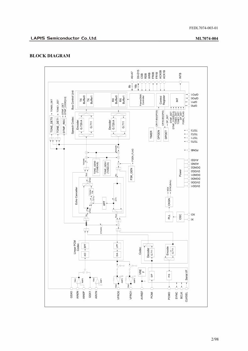
BLOCK DIAGRAM
Ech
o C
an
celle
r
DT
MF
_RE
C
+
-
AF
F
D/A
LPF
G.7
29.A
TO
NE
_G
EN
0(T
ON
EA
/B)
TX
Buf
fer0
RX
Buf
fer0
Fra
me/
DM
AC
ontr
olle
r
INT
B
A0-
A7
Co
ntr
ol
Re
gist
er
8b
D0-
D1
51
6b
VR
EF
CS
B
RD
B
WR
B
FR
0B
FR
1B
AC
K0B
AC
K1B
AIN
1N
GS
X1
VF
RO
0
AV
RE
F
OS
CP
ow
er
PL
L
Spe
ech
Cod
ec
10k
10k
DVDD2
DGND2
AVDD
AGND
PDNB
TST1
XI
XO
G.7
11
TX
GA
IN
RX
GA
IN
DVDD1
DGND1
DVDD0
DGND0
TST2
TST3
CK
GN
MC
KS
YN
C(8
kHz)
LP
AD
GP
AD
AT
Ts
AT
Tr
Bus
Co
ntro
l Un
it
Cen
ter
Clip
En
cod
er
G.7
29.A
G.7
11
De
code
r
DT
MF
_DE
T
INT
DT
MF
_DE
T
TX
Buf
fer1
RX
Buf
fer1
AIN
0N
GS
X0
10k
AIN
0P
Lin
ear
PC
MC
odec
VF
RO
110
k
ST
GA
IN
SY
NC
BC
LK
PC
MI
PC
MO
TO
NE
_D
ET
1T
ON
E1_
DE
T
S/P
P/S
Se
rial I
/F
TO
NE
0_D
ET
TO
NE
1_D
ET
GPI0
GPI1
GPO0
GPO1
TO
NE
_DE
T0
TO
NE
0_D
ET
FS
K_
GE
N
TST0
CLK
SE
L
AM
P0
AM
P1
AM
P2
AM
P3
Sin
Rou
t
Sou
t
Rin
A/D
BP
F
Co
dec
DP
GE
N
DP
DE
TC
R16
-B0(
GP
I0)
CR
17-B
0(G
PO
0)
DP
_DE
T
DP
_DE
T
TIM
ER
DT
MF
_CO
DE
[3:0
]
DT
MF
_CO
DE
[3:0
]
TO
NE
_GE
N1
(TO
NE
C/D
)
G.7
11
Enc
ode
r
G.7
11
Dec
oder
FG
EN
_FL
AG
FG
EN
_FLA
G

FEDL7074-003-01
ML7074-004
3/98
PIN ASSIGNMENT (TOP VIEW)
64-pin plastic QFP
49
AVREF
VFRO0
VFRO1
AVDD
50
51
52
53
54
55
56
57
58
59
60
61
62
63
64
32
31
30
29
28
27
26
25
24
23
22
21
20
19
18
17
D15
D14
D13
D12
D11
D10
D9
D8
D7
D6
D5
D4
D3
D2
D1
D0
48 47 46 45 44 43 42 41 40 39 38 37 36 35 34 33D
GN
D0
DG
ND
1
TST3
TST2
TS
T1
TS
T0
PC
MO
PC
MI
BC
LK
SY
NC
DV
DD
1
RD
B
WR
B
CS
B
FR
0B
FR
1B
DV
DD
0
A0
A1
A2
A3
A4
A5
A6
A7
DGND2
XI
XO
DVDD2
GP
I0
GP
I1
GP
O0
GP
O1
PD
NB
INT
B
AC
K0
B
AC
K1
B
CLK
SE
L
AIN1N
GSX1
AIN0P
AIN0N
GSX0
AGND
1 2 3 4 5 6 7 8 9 10
11
12
13
14
15
16
L7074-004

FEDL7074-003-01
ML7074-004
4/98
PIN DESCRIPTIONS Pin No.
Symbol I/O PDNB = “0” Description
1 TST1 I “0” Test control input 1: Normally input “0”. 2 TST0 I “0” Test control input 0: Normally input “0”. 3 PCMO O “Hi-z” PCM data output 4 PCMI I I PCM data input
I CLKSEL = “0” PCM shift clock input
5 BCLK I/O“L”
CLKSEL = “1” PCM shift clock output
I CLKSEL = “0” PCM sync signal 8 kHz input
6 SYNC I/O“L”
CLKSEL = “1” PCM sync signal 8 kHz output
7 DVDD0 Digital power supply 8 ACK0B I I Transmit buffer DMA access acknowledge signal input 9 ACK1B I I Receive buffer DMA access acknowledge signal input
10 FR0B
(DMARQ0B) O “H”
FR0B: (CR11-B7 = “0”) Transmit buffer frame signal output DMARQ0B: (CR11-B7 = “1”) Transmit buffer DMA access request signal output
11 FR1B
(DMARQ1B) O “H”
FR1B: (CR11-B7 = “0”) Receive buffer frame signal output DMARQ1B: (CR11-B7 = “1”) Receive buffer DMA access request signal output
12 INTB O “H” Interrupt request output “L” level is output for about 1.0 s when an interrupt is generated.
13 CSB I I Chip select control input 14 RDB I I Read control input 15 WRB I I Write control input 16 DGND0 I Digital ground (0.0 V) 17 D0 I/O I Data input/output 18 D1 I/O I Data input/output 19 D2 I/O I Data input/output 20 D3 I/O I Data input/output 21 D4 I/O I Data input/output 22 D5 I/O I Data input/output 23 D6 I/O I Data input/output 24 D7 I/O I Data input/output
25 D8 I/O I Data input/output Fix to input state when using in 8-bit bus access (CR11-B5 = “1”).
26 D9 I/O I Data input/output Fix to input state when using in 8-bit bus access (CR11-B5 = “1”).
27 D10 I/O I Data input/output Fix to input state when using in 8-bit bus access (CR11-B5 = “1”).
28 D11 I/O I Data input/output Fix to input state when using in 8-bit bus access (CR11-B5 = “1”).
29 D12 I/O I Data input/output Fix to input state when using in 8-bit bus access (CR11-B5 = “1”).
30 D13 I/O I Data input/output Fix to input state when using in 8-bit bus access (CR11-B5 = “1”).
31 D14 I/O I Data input/output Fix to input state when using in 8-bit bus access (CR11-B5 = “1”).
32 D15 I/O I Data input/output Fix to input state when using in 8-bit bus access (CR11-B5 = “1”).

FEDL7074-003-01
ML7074-004
5/98
Pin No.
Symbol I/O PDNB = “0” Description
33 DVDD1 Digital power supply 34 A0 I I Address input 35 A1 I I Address input 36 A2 I I Address input 37 A3 I I Address input 38 A4 I I Address input 39 A5 I I Address input 40 A6 I I Address input 41 A7 I I Address input
42 PDNB I “0” Power down input “0”: Power down reset “1”: Normal operation
43 CLKSEL I I SYNC and BCLK I/O control input “0”: SYNC and BCLK become inputs “1”: SYNC and BCLK become outputs
44 DGND1 Digital ground (0.0 V)
45 GPI0 I I General-purpose input pin 0 (5 V tolerant input) /Secondary function: Dial pulse detect input pin
46 GPI1 I I General-purpose input pin 1 (5 V tolerant input)
47 GPO0 O “L” General-purpose output pin 0 (5 V tolerant output, can be pulled up externally) /Secondary function: Dial pulse transmit pin
48 GPO1 O “L” General-purpose output pin 1 (5 V tolerant output, can be pulled up externally)
49 AVDD Analog power supply 50 AIN0P I I AMP0 non-inverted input 51 AIN0N I I AMP0 inverted input 52 GSX0 O “Hi-z” AMP0 output (10 k driving) 53 GSX1 O “Hi-z” AMP1 output (10 k driving) 54 AIN1N I I AMP1 inverted input 55 AVREF O “L” Analog signal ground (1.4 V) 56 VFRO0 O “Hi-z” AMP2 Output (10 k driving) 57 VFRO1 O “Hi-z” AMP3 Output (10 k driving) 58 AGND Analog ground (0.0 V) 59 DGND2 Digital ground (0.0 V) 60 XI I I 4.096 MHz crystal oscillator I/F, 4.096 MHz clock input 61 XO O “H” 4.096 MHz crystal oscillator I/F 62 DVDD2 Digital power supply 63 TST3 I “0” Test control input 3: Normally input “0”. 64 TST2 I “0” Test control input 2: Normally input “0”.
FEDL7074-003-01
ML7074-004
6/98
ABSOLUTE MAXIMUM RATINGS
Parameter Symbol Conditions Rating Unit Analog power supply voltage
VDA 0.3 to 5.0 V
Digital power supply voltage VDD 0.3 to 5.0 V Analog input voltage VAIN Analog pins 0.3 to VDD + 0.3 V
VDIN1 Normal digital pins 0.3 to VDD + 0.3 V Digital input voltage
VDIN2 5 V tolerant pins 0.3 to 6.0 V Storage temperature range Tstg 55 to +150 C
RECOMMENDED OPERATING CONDITIONS (Unless otherwise specified, AVDD = 3.0 to 3.6 V, DVDD0, 1, 2 = 3.0 to 3.6 V, AGND = DGND0, 1, 2 = 0.0 V, Ta = 20 to +60C)
Parameter Symbol Conditions Min. Typ. Max. Unit Analog power supply voltage VDA 3.0 3.3 3.6 V Digital power supply voltage VDD 3.0 3.3 3.6 V Operating temperature range Ta 20 60 C
VIH1 Digital input pins 2.0 VDD+ 0.3
V Digital high level input voltage
VIH2 GPI0 and GPI1 pins 2.0 5.5 V Digital low level input voltage VIL Digital pins 0.3 0.8 V Digital input rise time tIR Digital pins 2 20 ns Digital input fall time tIF Digital pins 2 20 ns Digital output load capacitance CDL Digital pins 50 pF Capacitance of bypass capacitor for AVREF
Cvref Between AVREF and AGND 2.2+0.1 4.7+0.1 F
Master clock frequency Fmck MCK 0.01% 4.096 +0.01% MHzPCM shift clock frequency Fbclk BCLK (at input) 64 2048 kHz PCM sync signal frequency Fsync SYNC (at input) 8.0 kHz Clock duty ratio DRCLK MCK, BCLK (at input) 40 50 60 %
tBS BCLK to SYNC
(at input) 100 ns
PCM sync timing tSB
SYNC to BCLK (at input)
100 ns
PCM sync signal width tWS SYNC (at input) 1BCLK 100 s

FEDL7074-003-01
ML7074-004
7/98
ELECTRICAL CHARACTERISTICS DC Characteristics (Unless otherwise specified, AVDD = 3.0 to 3.6 V, DVDD0, 1, 2 = 3.0 to 3.6 V, AGND = DGND0, 1, 2 = 0.0 V, Ta = 20 to +60C)
Parameter Symbol Conditions Min. Typ. Max. Unit
ISS Standby state
(PDNB = “0”, VDD = 3.3 V, Ta = 25C) 5.0 20.0 A
IDD1
Operating state 1 In the PCM/IF mode
(SC_EN = “1”, PCMIF_EN = “1”, AFE_EN = “1”)
Connect a 4.096 MHz crystal oscillator between XI and XO.
45.0 55.0 mA
Power supply current
IDD2
Operating state 2 When operating the whole system (SC_EN = “1”, PCMIF_EN = “0”,
AFE_EN = “0”) Connect a 4.096 MHz crystal oscillator
between XI and XO.
50.0 65.0 mA
IIH Vin = DVDD 0.01 1.0 A Digital input pin input leakage current IIL Vin = DGND 1.0 0.01 A
IOZH Vout = DVDD 0.01 1.0 A Digital I/O pin output leakage current IOZL Vout = DGND 1.0 0.01 A
High level output voltage
VOH Digital output pins, I/O pins
IOH = 4.0 mA IOH = 1.0 mA (XO pin)
2.2 V
Low level output voltage
VOL Digital output pins, I/O pins
IOL = 4.0 mA IOL = 1.0 mA (XO pin)
0.4 V
Input capacitance *1 CIN Input pins 8 12 pF Note: *1 Guaranteed design value

FEDL7074-003-01
ML7074-004
8/98
Analog Interface (Unless otherwise specified, AVDD = 3.0 to 3.6 V, DVDD0, 1, 2 = 3.0 to 3.6 V, AGND = DGND0, 1, 2 = 0.0 V, Ta = 20 to +60C)
Parameter Symbol Conditions Min. Typ. Max. Unit Input resistance *1 RIN AIN0N, AIN0P, AIN1N 10 M Output load resistance RL GSX0, GSX1, VFRO0, VFRO1 10 k Output load capacitance CL Analog output pins 50 pF Offset voltage VOF VFRO0, VFRO1 40 40 mV
Output voltage level *2 VO GSX0, GSX1, VFRO0, VFRO1
RL = 10 k 1.3 Vpp
Notes: *1 Guaranteed design value *2 7.7 dBm (600) = 0 dBm0, +3.17 dBm0 = 1.3 Vpp

FEDL7074-003-01
ML7074-004
9/98
AC Characteristics CODEC (Speech CODEC in G.711 (-law) Mode) (Unless otherwise specified, AVDD = 3.0 to 3.6 V, DVDD0, 1, 2 = 3.0 to 3.6 V, AGND = DGND0, 1, 2 = 0.0 V, Ta = 20 to +60C)
Conditions Parameter Symbol
Frequency (Hz) Level (dBm0) Min. Typ. Max. Unit
LT1 0 to 60 25 dB LT2 300 to 3000 0.15 0.20 dB LT3 1020 Reference value LT4 3300 0.15 0.80 dB LT5 3400 0 0.80 dB
Transmit frequency characteristics
LT6 3968.75
0
13 dB LR2 0 to 3000 0.15 0.20 dB LR3 1020 Reference value LR4 3300 0.15 0.80 dB LR5 3400 0 0.80 dB
Receive frequency characteristics
LR6 3968.75
0
13 dB SDT1 3 35 dBp SDT2 0 35 dBp SDT3 30 35 dBp SDT4 40 28 dBp
Transmit signal to noise ratio [*1]
SDT5
1020
45 23 dBp SDR1 3 35 dBp SDR2 0 35 dBp SDR3 30 35 dBp SDR4 40 28 dBp
Receive signal to noise ratio [*1]
SDR5
1020
45 23 dBp GTT1 3 0.2 0.2 dB GTT2 10 Reference value GTT3 40 0.2 0.2 dB GTT4 50 0.6 0.6 dB
Transmit inter-level loss error
GTT5
1020
55 1.2 1.2 dB GTR1 3 0.2 0.2 dB GTR2 10 Reference value GTR3 40 0.2 0.2 dB GTR4 50 0.6 0.6 dB
Receive inter-level loss error
GTR5
1020
55 1.2 1.2 dB
NIDLT Analog input =
AVREF 68 dBm0pIdle channel noise [*1]
NIDLR PCMI = “1” 72 dBm0pTransmit absolute level [*2]
AVT 1020 0 0.285 0.320 0.359 Vrms
Receive absolute level [*2]
AVR 1020 0 0.285 0.320 0.359 Vrms
PSRRT 30 dB Power supply noise reject ratio PSRRR
Noise frequency range: 0 to 50 kHz
Noise level: 50mVpp 30 dB
Notes: *1 Using P-message filter *2 0.320 Vrms = 0 dBm0 = 7.7 dBm (600)

FEDL7074-003-01
ML7074-004
10/98
Gain Setting (Speech CODEC in G.711 (-law) Mode) (Unless otherwise specified, AVDD = 3.0 to 3.6 V, DVDD0, 1, 2 = 3.0 to 3.6 V, AGND = DGND0, 1, 2 = 0.0 V, Ta = 20 to +60C)
Parameter Symbol Conditions Min. Typ. Max. Unit Transmit and receive gain setting accuracy
GAC 1.0 1.0 dB
Tone Output (Speech CODEC in G.711 (-law) Mode) (Unless otherwise specified, AVDD = 3.0 to 3.6 V, DVDD0, 1, 2 = 3.0 to 3.6 V, AGND = DGND0, 1, 2 = 0.0 V, Ta = 20 to +60C)
Parameter Symbol Conditions Min. Typ. Max. Unit Frequency deviation fDFT Relative to set frequency 1.5 1.5 % Output level oLEV Relative to set gain 2.0 2.0 dB
DTMF Detector, Other Detectors (Speech CODEC in G.711 (-law) Mode) (Unless otherwise specified, AVDD = 3.0 to 3.6 V, DVDD0, 1, 2 = 3.0 to 3.6 V, AGND = DGND0, 1, 2 = 0.0 V, Ta = 20 to +60C)
Parameter Symbol Conditions Min. Typ. Max. Unit Detect level accuracy dLAC Relative to set detect level 2.5 2.5 dB
Echo Canceller (Unless otherwise specified, AVDD = 3.0 to 3.6 V, DVDD0, 1, 2 = 3.0 to 3.6 V, AGND = DGND0, 1, 2 = 0.0 V, Ta = 20 to +60C)
Parameter Symbol Conditions Min. Typ. Max. Unit In the analog I/F mode
In the PCM I/F (16-bit linear) mode 35
Echo attenuation eRES In the PCM I/F (G.711) mode
30
dB
Erasable echo delay time tECT 32 ms Measurement method
Sin Sout
Delay
White noise generator
Rout Rin
ATT
E.R.L(echo return loss)
Echo delay time
Echo Canceller
LPF5 kHz
Level Meter
FEDL7074-003-01
ML7074-004
11/98
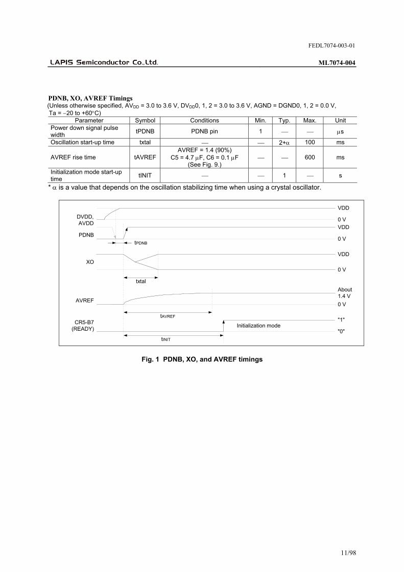
PDNB, XO, AVREF Timings (Unless otherwise specified, AVDD = 3.0 to 3.6 V, DVDD0, 1, 2 = 3.0 to 3.6 V, AGND = DGND0, 1, 2 = 0.0 V, Ta = 20 to +60C)
Parameter Symbol Conditions Min. Typ. Max. Unit Power down signal pulse width
tPDNB PDNB pin 1 s
Oscillation start-up time txtal 2+ 100 ms
AVREF rise time tAVREF AVREF = 1.4 (90%)
C5 = 4.7 F, C6 = 0.1 F (See Fig. 9.)
600 ms
Initialization mode start-up time
tINIT 1 s
* is a value that depends on the oscillation stabilizing time when using a crystal oscillator.
Fig. 1 PDNB, XO, and AVREF timings
PDNB
AVREF
About1.4 V
0 V
VDD
XO
0 V
VDD
txtal
0 V
tAVREF
DVDD,AVDD
0 V
VDD
tPDNB
"1"
"0"
CR5-B7(READY)
Initialization mode
tINIT

FEDL7074-003-01
ML7074-004
12/98
PCM I/F Mode (Unless otherwise specified, AVDD = 3.0 to 3.6 V, DVDD0, 1, 2 = 3.0 to 3.6 V, AGND = DGND0, 1, 2 = 0.0 V, Ta = 20 to +60C)
Parameter Symbol Conditions Min. Typ. Max. Unit Bit clock frequency fBCLK CDL = 20pF(at output) 0.1% 64 +0.1% kHz Bit clock duty ratio dBCLK CDL = 20pF(at output) 45 50 55 % Sync signal frequency fSYNC CDL = 20pF(at output) 0.1% 8 +0.1% kHz
dSYNC1CDL = 20pF(at output)
At 64 kHz output 12.4 12.5 12.6 %
Sync signal duty ratio dSYNC2
CDL = 20pF(at output) At 128 kHz output
6.24 6.25 6.26 %
tBS BCLK to SYNC
(at output) 100 ns
Transmit/receive signal sync timing
tSB SYNC to BCLK
(at output) 100 ns
Input setup time tDS 100 — ns Input hold time tDH 100 — ns
tSDX 100 ns Digital output delay time
tXD1 100 ns tXD2 100 ns
Digital output hold time tXD3
PCMO pin Pull-up, pull-down resistors RDL = 1 k, CDL = 50 pF
100 ns
0 1
MSB LSB
tWS
tDS tDH
BCLK
SYNC
PCMI
tBS tSB
2 3 4 5 6 7 8 - 16
G.711
LSB
16bitlinear
Fig. 2 PCM I/F mode input timing (long frame)
0 1
tWS
tDS tDH
BCLK
SYNC
PCMI
tBS tSB
2 3 4 5 6 7 8 9 -
MSB LSB
G.711
17
LSB
16bitlinear
Fig. 3 PCM I/F mode input timing (short frame)

FEDL7074-003-01
ML7074-004
13/98
0 1
LSB
tWS
BCLK
SYNC
PCMO
tBS tSB
2 3 4 5 6 7 8 9 -
MSBHi-z
tSDX tXD1 tXD2 tXD3
G.711
17
LSB
tXD3
16bitlinear
Fig. 4 PCM I/F mode output timing (long frame)
0 1
LSB
tWS
BCLK
SYNC
PCMO
tBS tSB
2 3 4 5 6 7 8 9 10
MSBHi-z
tXD1 tXD2 tXD3
G.711
- 18
LSB
16bitlinear
tXD3
Fig. 5 PCM I/F mode output timing (short frame)

FEDL7074-003-01
ML7074-004
14/98
Control Register Interface (Unless otherwise specified, AVDD = 3.0 to 3.6 V, DVDD0, 1, 2 = 3.0 to 3.6 V, AGND = DGND0, 1, 2 = 0.0 V, Ta = 20 to +60C)
Parameter Symbol Conditions Min. Typ. Max. Unit Address setup time tAS 10 ns Address hold time tAH 10 ns Write data setup time tWDS 10 ns Write data hold time tWDH 10 ns CSB setup time tCS 10 ns CSB hold time tCH 10 ns WRB pulse width tWW 10 ns Read data output delay time tRDD 20 ns Read data output hold time tRDH 3 ns RDB pulse width tRW 25 ns CSB disable time tCD
CL = 50 pF
10 ns
Fig. 6 Control register interface
A7-A0Input
D7-D0I/O
CSBInput
WRBInput
RDBInput
Write timing Read timing
tAS tAH
tWDS tWDH
tCH
tRDD
tCS
tRDH
tWW tRW
A1
D1Input
A2
D2Output
tCS tCH
tAS tAH
tCD

FEDL7074-003-01
ML7074-004
15/98
Transmit and Receive Buffer Interface (in Frame Mode) (Unless otherwise specified, AVDD = 3.0 to 3.6 V, DVDD0, 1, 2 = 3.0 to 3.6 V, AGND = DGND0, 1, 2 = 0.0 V, Ta = 20 to +60C)
Parameter Symbol Conditions Min. Typ. Max. Unit FR1B setup time tF1S 3 ns FR1B output delay time tF1D 20 ns Address setup time tAS 10 ns Address hold time tAH 10 ns Write data setup time tWDS 10 ns Write data hold time tWDH 10 ns CSB setup time tCS 10 ns CSB hold time tCH 10 ns WRB pulse width tWW 10 ns FR0B setup time tF0S 3 ns FR0B output delay time tF0D 20 ns Read data output delay time tRDD 30 ns Read data output hold time tRDH 3 ns RDB pulse width tRW 35 ns CSB disable time tCD
CL = 50 pF
10 ns
Fig. 7 Transmit and receive buffer interface (in frame mode)
A7-A0Input
D15-D0I/O
CSBInput
WRBInput
RDBInput
Write timing Read timing
tAS tAH
tWDS tWDH
tCH
tRDD
tCS
tRDH
tWW tRW
A1
D1Input
A2
D2Output
tCS tCH
tAS tAH
FR1BOutput
FR0BOutput
tF1S tF1D
tF0S tF0D
tCD
A7-A0Input
D15-D0I/O
CSBInput
WRBInput
RDBInput
Write timing Read timing
tAS tAH
tWDS tWDH
tCH
tRDD
tCS
tRDH
tWW tRW
A1
D1Input
A2
D2Output
tCS tCH
tAS tAH
FR1BOutput
FR0BOutput
tF1S tF1D
tF0S tF0D
tCD

FEDL7074-003-01
ML7074-004
16/98
Transmit and Receive Buffer Interface (in DMA Mode) (Unless otherwise specified, AVDD = 3.0 to 3.6 V, DVDD0, 1, 2 = 3.0 to 3.6 V, AGND = DGND0, 1, 2 = 0.0 V, Ta = 20 to +60C)
Parameter Symbol Conditions Min. Typ. Max. Unit DMARQ1B setup time tDR1S 3 ns
tDR1RD 25 ns DMARQ1B output delay time
tDR1FD 25 ns Address setup time tAS 10 ns Address hold time tAH 10 ns Write data setup time tWDS 10 ns Write data hold time tWDH 10 ns ACK setup time tAKS 10 ns ACK hold time tAKH 10 ns WRB pulse width tWW 10 ns DMARQ0B setup time tDR0S 3 ns
tDR0RD 20 ns DMARQ0B output delay time
tDR0FD 25 ns Read data output delay time tRDD 30 ns Read data output hold time tRDH 3 ns RDB pulse width tRW 35 ns ACKB disable time tAD
CL = 50 pF
10 ns
Fig. 8 Transmit and receive buffer interface (in DMA mode)
A7-A0Input
D15-D0I/O
ACK0BInput
WRBInput
RDBInput
Write timing Read timing
tAS tAH
tWDS tWDH tRDD
tAKS
tRDH
tWW tRW
A1
D1Input
A2
D2Output
tAKH
tAS tAH
DMARQ1BOutput
DMARQ0BOutput
tDR1S
tDR1RD
tDR0S
tDR0RD
ACK1BInput
tAKHtAKS tAD
tDR1FD
tDR0FD

FEDL7074-003-01
ML7074-004
17/98
PIN FUNCTION DESCRIPTIONS AIN0N, AIN0P, GSX0, AIN1N, GSX1 These are the analog transmit input and transmit level adjust pins. Each of AIN0N and AIN1N is connected to each of the inverting input pins of the built-in transmit amplifiers AMP0 and AMP1, and AIN0P is connected to the non-inverting input pin of AMP0. In addition, GSX0 and GSX1 are connected to the output pins of AMP0 and AMP1, respectively. The selection between AMP0 and AMP1 is made by CR10-B0. See Fig. 9 for the method of making level adjustment. During the power down mode (when PDNB = “0” or CR0-B7 = “1”), the outputs of GSX0 and GSX1 go to the high impedance state. If AMP0 is not used in the specific application of this LSI, short GSX0 with AIN0N and connect AIN0P with AVREF. When AMP1 is not used, short GSX1 with AIN1N. Notice: It is recommended to select the amplifier to be used before the conversation starts, since a small amount of noise will be generated if the amplifier selection is changed while conversation is in progress. VFRO0, VFRO1 These are analog receive output pins and are connected to the output pins of the built-in receive amplifiers AMP2 and AMP3, respectively. The output signals of VFRO0 and VFRO1 can be selected using CR10-B1 and CR10-B2, respectively. When selected (“1”), the received signal will be output, and when deselected (“0”), the AVREF signal (about 1.4 V) will be output. In the power down mode, these pins will be in the high impedance state. It is recommended to use these output signals via DC coupling capacitors. Notice: It is recommended to select the amplifier to be used before the conversation starts, since a small amount of noise is generated if the output selection is changed while the conversation is in progress. At the time of resetting or releasing from the reset state, it is recommended to select the AVREF as outputs of VFRO0 and VFRO1.
Fig. 9 Analog interface
R1
R2
A/D
D/A
VREF
AIN1N
GSX1
AVREF
AIN0N
GSX0
10k
AIN0P
R3
R4
C6 0.1F
C1
C2
C3
C4
VFRO010k
VFRO110k
C52.2 to 4.7F
CR10-B0
CR10-B1
CR10-B2
Gain = R2/R1 <= 63(+36dB)R1 : VariableR2 : Max 500k
+
Gain = R4/R3 <=63(+36dB)R3 : VariableR4 : Max 500k
Out : Max 1.3Vp-p
Out : Max 1.3Vp-p
AMP0
AMP1
AMP3
AMP2

FEDL7074-003-01
ML7074-004
18/98
AVREF This is the output pin for the analog signal ground potential. The output potential at this pin will be about 1.4 V. Connect a 2.2 to 4.7 F (aluminum electrolytic type) capacitor and a 0.1 F (ceramic type) capacitor in parallel between this pin and the GND pin as bypass capacitors. The output at the AVREF pin goes to 0.0 V in the power down mode. The voltage starts rising after the power down mode is released (PDNB = “1” and also CR0-B7 = “0”). The rise time is about 0.6 seconds. XI, XO These are the pins for either connecting the crystal oscillator for the master clock or for inputting an external master clock signal. The oscillations of the master clock oscillator will be stopped during a power down due to the PDNB signal or during a software power down due to CR0-B7 (SPDN). The oscillations start when the power down condition is released, and the internal clock supply of the LSI will be started after counting up the oscillation stabilization period (of about 16 ms). Examples of crystal oscillator connection and external master clock input are shown in Fig. 10.
Fig. 10 Examples of oscillator circuit and clock input PDNB This is the power down control input pin. The power down mode is entered when this pin goes to “0”. In addition, this pin also has the function of resetting the LSI. In order to prevent wrong operation of the LSI, carry out the initial power-down reset after switching on the power using this PDNB pin. Also, keep the PDNB pin at “0” level for 1 s or more to initiate the power down state. Further, it is possible to carry out a power down reset of the LSI when the power is being supplied by performing control of CR0-B7 (SPDN) in the sequence “0” “1” “0”. The READY signal (CR5-B7) goes to “1” about 1.0 second after the power down mode is released thereby entering the mode of setting various functions (initialization mode). See Fig. 1 for the timings of PDNB and AVREF, XO, and the initialization mode. Notice: At the time of switching on the power, start from the power down mode using PDNB. DVDD0, DVDD1, DVDD2, AVDD These are power supply pins. DVDD0, 1, 2 are the power supply pins for the digital circuits while AVDD is the power supply pin for the analog circuits of the LSI. Connect these pins together in the neighborhood of the LSI and connect as bypass capacitors a 10 F electrolytic capacitor and a 0.1 F ceramic capacitor in parallel between the DGND and AGND pins. DGND0, DGND1, DGND2, AGND These are ground pins. GDND0, 1, 2 are the ground pins for the digital circuits and AGND is the ground pin for the analog circuits of the LSI. Connect these pins together in the neighborhood of the LSI.
XI XOR
X'tal
C1 C2
4.096 MHz
X'tal(4.096 MHz)
Daishinku Co., Ltd.AT-49
C2 R
10pF 1M
PDNB
To internalcircuits
CR0-B7(SPDN)
XI XOOpen
PDNB
To internalcircuits
CR0-B7(SPDN)
C1
5pF

FEDL7074-003-01
ML7074-004
19/98
TST0, TST1, TST2, TST3 These are input pins for testing purposes only. Keep the inputs to these pins at the “0” level during normal use conditions. INTB This is the interrupt request output pin. An “L” level is output for a duration of about 1.0 s at this pin when there is a change in state of an interrupt cause. This output will be maintained at the “H” level when there is no change in state of any of the interrupt causes. The actual interrupt cause generating the interrupt can be verified by reading CR3, CR4, and CR5. The different interrupt causes are described below. Underflow error (CR3-B0)
An interrupt is generated when an internal read from the receive buffer occurs before the writing into the receive buffer from the MCU has been completed. An interrupt is generated when a normal writing is made in the receive buffer by the MCU and the underflow error is released.
Overrun error (CR3-B1)
An interrupt is generated when an internal write of the next data into the transmit buffer occurs before the transmit buffer data read out from the MCU has been completed. An interrupt is generated when a normal read out is made from the transmit buffer by the MCU and the overrun error is released.
When a dial pulse is detected (CR4-B6). When a DTMF signal is detected (CR4-B4). When DTMF_CODEC0, 1, 2, 3 are detected (CR4-B0, B1, B2, B3).
An interrupt is generated when a DTMF signal is detected. An interrupt is generated when there is a change from the DTMF signal detected state to the no-detected state. An interrupt is generated when there is a change in the detected code (CR4-B0, B1, B2, B3) in the condition in which a DTMF signal is being detected.
When TONE0 is detected (CR3-B3).
An interrupt is generated when a 1650 Hz tone signal is detected. An interrupt is generated when there is a change to the non-detection condition in the tone signal detection condition.
When TONE1 is detected (CR3-B4).
An interrupt is generated when a 2100 Hz tone signal is detected. An interrupt is generated when there is a change to the non-detection condition in the tone signal detection condition.
When DSP_ERR is detected (CR3-B7).
An interrupt is generated when any error occurs in the DSP inside the LSI. When FGEN_FLAG is cleared (CR5-B0).
FGEN_FLAG is cleared to “0” and an interrupt is generated when data settings are enabled to output data setting register FGEN_D[7:0] (CR18) in the FSK generator.

FEDL7074-003-01
ML7074-004
20/98
A0 to A7 These are the address input pins for use during an access of the frame, DMA, or control registers. The different addresses will be the following. Transmit buffer (TX Buffer) A7 to A0 = 10xxxxxxb (the lower 6 bits are not valid) Receive buffer (RX Buffer) A7 to A0 = 01xxxxxxb (the lower 6 bits are not valid) Control register (CR) A7 to A0 = 00xxxxxxb D0 to D15 These are the data input/output pins for use during an access of the frame, DMA, or control registers. Connect pull-up resistors to these pins since they are I/O pins. When the 8-bit bus access method is selected by CR11-B5, only D0 to D7 become valid. Since the higher 8 bits D8 to D15 will always be in the input state when the 8-bit bus access method is selected (CR11-B5 = “1”), tie them to “0” or “1” inputs. CSB This is the chip select input pin for use during a frame or control register access. RDB This is the read enable input pin for use during a frame, DMA, or control register access. WRB This is the write enable input pin for use during a frame, DMA, or control register access.

FEDL7074-003-01
ML7074-004
21/98
FR0B (DMARQ0B) FR0B (In frame mode, CR11-B7 = “0”) This is the transmit frame output pin which outputs the signal when the transmit buffer is full during frame
access. This pin outputs an “L” level when the transmit buffer becomes full, and maintains that “L” level output until a specific number of words are read out from the MCU.
DMARQ0B (In DMA mode, CR11-B7 = “1”) This is the DMA request output pin which outputs the signal when the transmit buffer is full during DMA access.
This output becomes “L” when the transmit buffer becomes full, and returns to the “H” level automatically on the falling edge of the read enable signal (RDB = “1” “0”) when there is an acknowledgement signal (ACK0B = “0”) from the MCU. This relationship is repeated until a specific number of words are read out from the MCU.
FR1B (DMARQ1B) FR1B (In frame mode, CR11-B7 = “0”) This is the receive frame output pin which outputs the signal when the receive buffer is empty during frame
access. This pin outputs an “L” level when the receive buffer becomes empty, and maintains that “L” level output until a specific number of words are written from the MCU.
DMARQ1B (In DMA mode, CR11-B7 = “1”) This is the DMA request output pin which outputs the signal when the receive buffer is empty during DMA
access. This output becomes “L” when the receive buffer becomes empty, and returns to the “H” level automatically on the falling edge of the write enable signal (WRB = “1” “0”) when there is an acknowledgement signal (ACK1B = “0”) from the MCU. This relationship is repeated until a specific number of words are written from the MCU.
ACK0B This is the DMA acknowledgement input pin for the DMARQ0B signal during DMA access of the transmit buffer and becomes valid in the DMA mode (CR11-B7 = “1”). Tie this pin to “1” when using this LSI in the frame access mode (CR11-B7 = “0”). ACK1B This is the DMA acknowledgement input pin for the DMARQ1B signal during DMA access of the receive buffer and becomes valid in the DMA mode (CR11-B7 = “1”). Tie this pin to “1” when using this LSI in the frame access mode (CR11-B7 = “0”). GPI0, GPI1 These are general-purpose input pins. The state (“1” or “0”) of each of these GPI0 and GPI1 pins can be read out respectively from CR16-B0 and CR16-B1. Further, GPI0 becomes the input pin for the dial pulse detector (DPDET) in the secondary functions. GPO0, GPO1 These are general-purpose output pins. The values set in CR17-B0 and CR17-B1 are output at these pins GPO0 and GPO1, respectively. Further, GPO0 becomes the output pin for the dial pulse generator (DPGEN) in the secondary functions.

FEDL7074-003-01
ML7074-004
22/98
CLKSEL This is the input/output control input pin of SYNC and BCLK. The pin becomes input at “0” level and output at “1” level. SYNC This is the 8 kHz sync signal input/output pin of PCM signals. When CLKSEL is “0”, input continuously an 8 kHz clock synchronous with BCLK. Further, when CLKSEL is “1”, this pin outputs an 8 kHz clock synchronous with BCLK. Long frame synchronization is used when CR0-B1 (LONG/SHORT) is “0” and short frame synchronization is used when it is “1”. BCLK This is the shift clock input/output pin for the PCM signal. When CLKSEL is “0”, it is necessary to input to this pin a clock signal that is synchronous with SYNC. Input a 64 to 2048 kHz clock when the G.711 mode has been selected, and input a 128 to 2048 kHz clock when the 16-bit linear mode has been selected. When CLKSEL is “1”, this pin outputs a clock that is synchronous with SYNC. This pin outputs a 64 kHz clock when the G.711 mode has been selected, and outputs an 128 kHz clock when the 16-bit linear mode or G.729.A mode has been selected. Note: The input/output control and frequencies of the above SYNC and BLCK signals will be as shown in Table 1
below.
Table 1 Input/output control of SYNC and BCLK CLKSEL SYNC BCLK Remarks
“0” Input
(8 kHz) Input
(64 kHz to 2048 kHz)
Input a continuous clock after starting the power supply. Input a 64 to 2048 kHz clock when G.711 is selected.Input a 128 to 2048 kHz clock when 16-bit linear mode is selected.
“1” Output (8 kHz)
Output (64 kHz or 128 kHz)
An “L” level is output during the power down mode.A 64 kHz clock is output when G.711 is selected. A 128 kHz clock is output when G.729.A or 16-bit linear mode is selected.
PCMO This is the PCM signal output pin for the transmitting section. The PCM signal is output in synchronization with the rising edges of SYNC and BCLK. The PCMO outputs the data only during the valid data segment in the selected coding format and goes to the high impedance state during all other segments. The basic timing chart of the PCM I/F mode is shown in Fig. 11. The PCMO output will be in the high impedance state when the PCM I/F mode is not used (CR12-B0 = “0”). PCMI This is the PCM signal input pin for the receiving section. The data is entered starting from the MSB by shift on the falling edge of BCLK. The basic timing chart of the PCM I/F mode is shown in Fig. 11. Fix input to “0” or “1” when the PCM I/F mode (CR12-B0 = “0”) is not used.

FEDL7074-003-01
ML7074-004
23/98
Fig. 11 PCM I/F mode timing diagram
BCLK(IN/OUT))
PCMI
SYNC(IN/OUT)
- 16-Bit linear- Long frame synchronization mode (CR0-B1="0")
D7
D6
D5
D4
D3
D2
D1
D0
D7
D6
D5
D4
D3
D2
D1
D0
BCLK(IN/OUT)
PCMO
SYNC(IN/OUT))
- G.711(-law,A-law)- Short frame synchronization mode(CR0-B1="1")
D7
D6
D5
D4
D3
D2
D1
D0
D7
D6
D5
D4
D3
D2
D1
D0Hi-zHi-z Hi-z
PCMO D7
D6
D5
D4
D3
D2
D1
D0
D7
D6
D5
D4
D3
D2
D1
D0Hi-zHi-z Hi-z
PCMI D7
D6
D5
D4
D3
D2
D1
D0
D7
D6
D5
D4
D3
D2
D1
D0
BCLK(IN/OUT))
PCMI
SYNC(IN/OUT)
D15
D14
D13
D12
D11
D10 D9
D8
BCLK(IN/OUT)
PCMO
SYNC(IN/OUT))
- 16-Bit linear- Short frame synchronization mode (CR0-B1="1")
Hi-z
PCMOHi-zHi-z
PCMID
7
D6
D5
D4
D3
D2
D1
D0
D7
D6
D5
D4
D3
D2
D1
D0
D15
D14
D13
D12
D11
D10 D9
D8
D15
D14
D13
D12
D11
D10 D9
D8
D7
D6
D5
D7
D6
D5
D15
D14
D13
D12
D11
D10 D9
D8
D15
D14
D13
D12
D11
D10 D9
D8
Hi-z
D7
D6
D5
D4
D3
D2
D1
D0
D7
D6
D5
D4
D3
D2
D1
D0
D15
D14
D13
D12
D11
D10 D9
D8
D15
D14
D13
D12
D11
D10 D9
D8
D7
D6
D7
D6
D15
D14
D13
D12
D11
D10 D9
D8
- G.711(-law,A-law)- Long frame synchronization mode (CR0-B1="0")

FEDL7074-003-01
ML7074-004
24/98
FUNCTION DESCRIPTION On the Transmit and Receive Buffers The controllable parameters of the transmit and receive buffers are shown in Table 2 below.
Table 2 Controllable parameters of transmit and receive buffers Content Changeable parameter Initial value Remarks
Speech CODEC G.729.A/G.711(-law, A-law)
G.729.AThe buffering size of the FIFO is changed automatically depending on the speech CODEC type.
Buffering time 10 ms/20 ms 10 ms The number of words is changed automatically depending on the buffering time.
Accessing method
Frame or DMA Frame
FIFO data width 16-bit/8-bit 16-bit The number of words is changed automatically depending on the data width.
Transmit and Receive Buffer Sizes The transmit and receive buffers have a double buffer configuration of the FIFO (First In First Out) type, and one buffer can buffer data of 10 ms or 20 ms. The timing of generation of the frame signals (FR0B, FR1B) requested to the MCU when the transmit buffer is full or the receive buffer is empty, and the timing of generation of the DMA request signals (DMARQ0B, DMARQ1B) depend on the buffering time. Further, the number of words of FIFO is changed automatically depending on the selected speech CODEC type and the FIFO data width. The buffer size and the number of words for the different speech CODEC types and data widths are shown in Table 3.
Table 3 Buffer size and number of words of transmit and receive buffers 10 ms mode 20 ms mode
Speech CODEC Buffer size 16-bit 8-bit Buffer size 16-bit 8-bit
G.729.A (8 kbps) 10 bytes 5 words 10 words 20 bytes 10 words 20 words
G.711 (64 kbps) 80 bytes 40 words 80 words 160 bytes 80 words 160 words
FEDL7074-003-01
ML7074-004
25/98
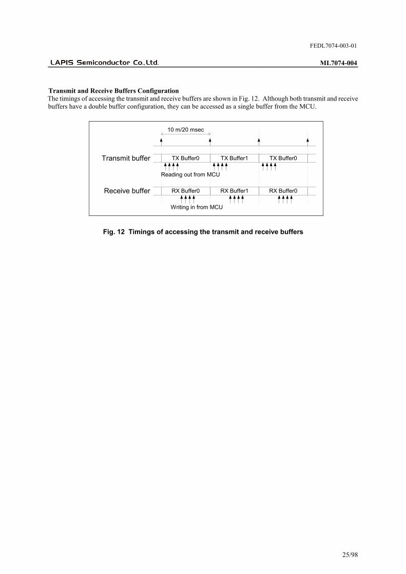
Transmit and Receive Buffers Configuration The timings of accessing the transmit and receive buffers are shown in Fig. 12. Although both transmit and receive buffers have a double buffer configuration, they can be accessed as a single buffer from the MCU.
Fig. 12 Timings of accessing the transmit and receive buffers
Transmit buffer TX Buffer0
10 m/20 msec
Receive buffer RX Buffer0
Writing in from MCU
Reading out from MCU
TX Buffer1 TX Buffer0
RX Buffer1 RX Buffer0

FEDL7074-003-01
ML7074-004
26/98
Data Width Selection (16-Bit Mode, 8-Bit Mode) In the method of accessing the transmit and receive buffers, it is possible to select data width of 16 bits or 8 bits using the control register bit CR11-B5. During the 16-bit mode, the access is made with a data width of 16 bits and the data bits D15 to D0 are accessed. In the 8-bit mode, the transmit and receive data are input or output to D7 to D0. During the 8-bit access mode, the bits D15 to D8 will always be in the input state. Data Storage Format The data storage formats during transmission and reception depending on the settings of the different parameters are shown in Fig. 13 and Fig. 14.
A. G.729.A
Fig. 13 G.729.A data format
G.729.A(8 kbps) 1 frame 80-bit/10 ms 2 frames 160-bit/20 ms
bit15 ························ bit0
bit31 ······················· bit16
bit63 ······················· bit48
bit79 ······················· bit64
(a) 10 ms/16-bit mode (b) 20 ms/16-bit mode
Firs
t fr
ame
bit7 ··········· bit0
··
(c) 10 ms/8-bit mode
Firs
t fr
ame bit15 ·········· bit8
bit71··········· bit64
bit79··········· bit72
··
(d) 20 ms/8-bit mode
D15 D0
··
D15 D0
D7 D0 D7 D0
Wordcount
1
2
4
5
bit47 ······················· bit323
Wordcount
1
2
·9
·
10
bit7 ·········· bit0
bit15 ·········· bit8
bit71·········· bit64
bit79·········· bit72
bit7··········· bit0
bit15·········· bit8
bit71·········· bit64
bit79·········· bit72
bit15 ···························· bit0
bit31 ···························· bit16
bit63 ···························· bit48
bit79 ···························· bit64
bit47 ···························· bit32
bit15 ···························· bit0
bit31 ···························· bit16
bit63 ···························· bit48
bit79 ···························· bit64
bit47 ···························· bit32
Firs
t fr
ame
Sec
ond
fram
e
Wordcount
1
2
·9
·
10
11
··
12
19
20
Firs
t fr
ame
Wordcount
1
2
4
5
3
6
7
9
10
8
Sec
ond
fram
e
GB20
GB21
GB22
GB23
GA20
GA21
GA22
S20
S21
S22
S23
C20
C21
C22
C23
C24
C25
C26
C27
C28
C29
C210
C211
C212
P20
P21
P22
P23
P24
GB10
GB11
GB12
GB13
GA10
GA11
GA12
S10
S11
S12
S13
C10
C11
C12
C13
C14
C15
C16
C17
C18
C19
C110
C111
C112
P0P10
P11
P12
P13
P14
P15
P16
P17
L30
L31
L32
L33
L34
L20
L21
L22
L23
L24
L0
Wordcount
1
2
4
5
3
L10
L11
L12
L13
L14
L15
L16
B15 B14 B13 B12 B11 B10 B9 B8 B7 B6 B5 B4 B3 B2 B1 B0
G.729.A coding, Word configuration
Word configuration
Symbol namebit No.

FEDL7074-003-01
ML7074-004
27/98
B. G.711 (64 kbps)
Fig. 14 G.711 data format
G.711(64 kbps, -law/A-law) 8 bit/125 sBuffer configuration 80 samples/10 ms 160 samples/20 ms
··
(a) 10 ms/16-bit mode
(b) 20 ms/16-bit mode
bit7 bit6 bit5 bit4
PCM coding configuration
·········
bit3 bit2 bit1 bit0
10
3
157156
159158
0
··
(c) 10 ms/8-bit mode
78
79
(d) 20 ms/16-bit mode
Word configuration
1
2
39
40
.
.
1
2
79
80
.
.
1
2
79
80
.
.
0
······
158
159
1
2
159
160
.
.
Wordcount
Wordcount
Wordcount
Wordcount
10
3
7776
7978
bit7···bit0 bit7···bit0
2 2
bit7····bit0 2
11
bit7····bit0
D15 D0
D7 D0
D15 D0
D7 D0

FEDL7074-003-01
ML7074-004
28/98
Tra
nsm
it a
nd
Rec
eive
Bu
ffer
Con
trol
Met
hod
T
he m
etho
ds o
f co
ntro
llin
g th
e tr
ansm
it a
nd r
ecei
ve b
uffe
rs d
epen
ding
on
the
diff
eren
t par
amet
ers
are
show
n in
Fig
s. 1
5 to
18.
A
. G
.729
.A (
10 m
s/fr
ame
mod
e)
Fig
. 15
G.7
29.A
co
ntr
ol t
imin
g (
10 m
s/fr
ame
mo
de)
FR
0B
(ou
tpu
t)
Re
ad
ou
t by
MC
UR
ea
d o
ut
valid
seg
me
nt
4)
Err
or
TX
_ER
R(C
R3
-B1
)
10
ms
EN
CS
pe
ech
CO
DE
CIn
itT
1T
2T
3T
4T
5T
8T
6T
7S
top
pd
eT
9
SC
_EN
(CR
2-B
7)
1)
Sta
rt M
axi
mu
m 2
50
s
2)
Op
era
ting
3)
Sto
p M
axi
mu
m 2
50
s
5)
Sta
rt in
terv
al 1
0.0
ms
or
mo
re
Sto
pp
ed
RE
1R
E2
RE
3R
E4
RE
5R
E6
RE
7R
E8
INIT
Ab
ou
t 1
25
s
10
ms
Sp
ee
chC
OD
EC
No
-to
ne
ou
tpu
tD
EC
OU
TN
o-t
on
e o
utp
ut/
Init
No-
tone
out
put/
Init
FR
1B
(ou
tpu
t)
Wri
te in
by
MC
UW
rite
va
lid s
eg
me
nt
WE
1
INT
B(o
utp
ut)
RX
_E
RR
(CR
3-B
0)
DE
C_
OU
TO
N(C
R2
-B5
)
WE
2W
E3
WE
4W
E5
WE
6W
E7
WE
8W
E 9W
E1
0
tWA
IT
Ab
ou
t 1
5 m
s
R5
R6
R7
R8
R1
R2
R3
R4
(B
FI)
No
-to
ne
ou
tpu
tN
o-
ton
e
Ab
ou
t12
5
s
4) E
rro
r
10
ms
1) S
tart
D
EC
_OU
TO
N “
0”,
SC
_E
N “
0”
“1”
The
spe
ech
CO
DE
C s
tart
s w
ithin
abo
ut 2
50 s
afte
r S
C_E
N h
as b
een
set t
o “1
”. T
he e
nco
der
is in
itial
ized
dur
ing
the
first
10
ms
peri
od,
and
star
ts e
ncod
ing
with
th
e T
1 se
gme
nt.
T
he d
eco
der
carr
ies
out
initi
aliz
atio
n af
ter
the
spe
ech
CO
DE
C h
as b
een
sta
rte
d, a
nd o
utp
uts
no-t
one
dat
a.
If
the
first
rec
eive
dat
a ha
s be
en w
ritte
n a
nd t
he t
WA
IT w
ait
time
has
ela
psed
, th
e D
EC
out
put
con
tro
l bit
(DE
C_O
UT
ON
) ca
n be
set
to
“1”.
(tW
AIT
= 1
ms
or m
ore)
The
dec
ode
r st
arts
dec
oder
out
put
abo
ut 1
5 m
s af
ter
DE
C_O
UT
ON
is s
et t
o “1
”.
2) O
pera
ting
T
he d
ata
enc
ode
d du
ring
enc
ode
seg
me
nt T
n is
rea
d by
the
MC
U d
urin
g re
ad v
alid
seg
men
t RE
n. T
his
ope
ratio
n is
re
peat
ed u
ntil
the
spee
ch C
OD
EC
is s
topp
ed.
(n =
1, 2
, 3,
4, …
)
The
dat
a w
ritte
n by
the
MC
U d
urin
g w
rite
va
lid s
egm
ent
WE
n is
ou
tput
dur
ing
deco
der
outp
ut s
egm
ent
Rn.
Thi
s op
erat
ion
is r
epea
ted
until
the
spe
ech
CO
DE
C is
sto
pped
. (n
= 1
, 2,
3, 4
, …
) 3)
Sto
p
Set
SC
_E
N “
1”
“0”
, DE
C_O
UT
ON
“1”
“
0”
E
ncod
ing
an
d de
codi
ng
afte
r th
e st
opp
age
of t
he s
pee
ch C
OD
EC
is d
isa
bled
.
With
in a
bou
t 25
0 s
afte
r S
C_E
N h
as b
een
set t
o “1
”, t
he e
nco
der
stop
s w
ritin
g d
ata
, an
d th
e de
code
r st
ops
and
then
out
put
s no
-to
ne d
ata.
4)
Err
or p
roce
ssin
g
Rec
eive
err
or:
In
the
figu
re a
bove
, an
exa
mpl
e of
a r
ecei
ve e
rror
occ
urre
nce
is s
how
n in
the
writ
e va
lid s
egm
ent W
E4.
If da
ta w
ritin
g is
not
com
ple
ted
with
in a
writ
e va
lid s
egm
ent,
RX
_ER
R is
set
to
“1”
and
an in
terr
upt
is g
ener
ated
. The
sta
te o
f R
X_E
RR
will
be
ma
inta
ined
dur
ing
and
afte
r th
e n
ext
writ
e va
lid
se
gmen
t un
til ju
st b
efor
e th
e en
d o
f a
fram
e th
at h
as b
een
wri
tten
norm
ally
into
th
e R
X b
uffe
r.
If
an e
rror
occ
urs
in th
e w
rite
valid
seg
men
t WE
4, th
e lo
ss-o
f-fr
ame
com
pens
atio
n p
roce
ssin
g (B
FI:
Bad
Fra
me
Ind
icat
or)
spec
ifie
d in
G.7
29A
will
be
perf
orm
ed.
T
rans
mit
erro
r:
In
the
figu
re a
bove
, an
exa
mpl
e of
a tr
ansm
it er
ror
occu
rren
ce is
sho
wn
in th
e re
ad
valid
seg
men
t RE
5.
If
data
rea
din
g is
not
com
plet
ed w
ithin
a r
ead
valid
se
gm
ent,
TX
_ER
R is
set
to “
1” a
nd a
n in
terr
upt i
s g
ener
ate
d. T
he s
tate
of T
X_E
RR
will
be
mai
ntai
ned
dur
ing
and
afte
r th
e ne
xt r
ead
valid
segm
ent u
ntil
just
bef
ore
the
end
of
a fr
ame
that
has
bee
n re
ad n
orm
ally
fro
m th
e tr
ansm
it bu
ffer.
Eve
n if
data
rea
ding
is n
ot c
omp
lete
d, t
he d
ata
in th
e tr
ans
mit
buffe
r is
upd
ated
as
usua
l. 5)
Sta
rt in
terv
al
A
n in
terv
al o
f 10
.0 m
s or
mor
e is
req
uire
d af
ter
the
spe
ech
CO
DE
C h
as s
topp
ed b
efor
e it
is s
tart
ed
aga
in. D
urin
g th
is in
terv
al,
it is
pos
sibl
e to
cha
nge
the
spe
ech
CO
DE
C.
W
rite
valid
seg
men
t: T
here
is n
o re
stric
tion
of t
ime
on
the
first
wri
te v
alid
seg
men
t (W
E1)
afte
r th
e sp
eec
h C
OD
EC
is s
tart
ed.
F
or th
e w
rite
va
lid s
egm
ent
WE
2 an
d af
ter,
com
plet
e th
e w
ritin
g of
dat
a to
the
RX
buf
fer
with
in 9
.0 m
s fr
om
the
falli
ng e
dge
of F
R1B
.
Rea
d va
lid s
egm
ent:
Co
mpl
ete
the
rea
ding
of d
ata
from
the
TX
buf
fer
with
in 9
.0 m
s fr
om th
e fa
llin
g ed
ge o
f FR
0B.

FEDL7074-003-01
ML7074-004
29/98
Fig
. 16
G.7
29.A
co
ntr
ol t
imin
g (
20 m
s/fr
ame
mo
de)
B.
G.7
29.A
(20
ms/
fram
e m
ode)
FR
0B
(ou
tput
)
Rea
d o
ut b
y M
CU
Rea
d o
ut
valid
seg
men
t
4) E
rror
TX
_ER
R(C
R3
-B1)
20 m
s
EN
CS
pee
chC
OD
EC
Init
T1
T3
T5
T7
Sto
ppe
dT
9
SC
_E
N(C
R2
-B7)
1) S
tart
Max
imum
250
s
2)
Ope
ratin
g3
) S
top
Ma
xim
um
250
s
5) S
tart
inte
rva
l 10.
0 m
s o
r m
ore
Sto
pped
RE
1R
E3
RE
5R
E7
INIT
FR
1B
(ou
tput
)
Writ
e in
by
MC
UW
rite
val
id s
egm
ent
INT
B(o
utp
ut)
RX
_ER
R(C
R3
-B0)
WE
1
DE
C_
OU
TO
N(C
R2
-B5)
Ab
out
125 s
Abo
ut 1
0 m
s
20 m
s
Spe
ech
CO
DE
CN
o-to
ne
outp
utD
EC
OU
TN
o-t
one
out
put/I
nit
20 m
s
Abo
ut 1
5 m
s
4) E
rror
WE
3W
E5
WE
7W
E9
WE
11
Abo
ut 1
25 s
tWA
IT
R5
(BF
I)R
7R
1R
3N
o-t
one
outp
utN
o-to
neo
utp
ut/I
nit
No
-ton
e
1) S
tart
D
EC
_OU
TO
N “
0”,
SC
_E
N “
0”
“1”
The
spe
ech
CO
DE
C s
tart
s w
ithin
abo
ut 2
50 s
afte
r S
C_E
N h
as b
een
set t
o “1
”. T
he e
nco
der
is in
itial
ized
dur
ing
the
first
10
ms
peri
od,
and
star
ts e
ncod
ing
with
th
e T
1 se
gme
nt.
T
he d
eco
der
carr
ies
out
initi
aliz
atio
n af
ter
the
spe
ech
CO
DE
C h
as b
een
sta
rte
d, a
nd o
utp
uts
no-t
one
dat
a.
If
the
first
rec
eive
dat
a ha
s be
en w
ritte
n a
nd t
he t
WA
IT w
ait
time
has
ela
psed
, th
e D
EC
out
put
con
tro
l bit
(DE
C_O
UT
ON
) ca
n be
set
to
“1”.
(tW
AIT
= 1
ms
or m
ore)
The
dec
ode
r st
arts
dec
oder
out
put
abo
ut 1
5 m
s af
ter
DE
C_O
UT
ON
is s
et t
o “1
”.
2) O
pera
ting
T
he d
ata
enc
ode
d du
ring
enc
ode
seg
me
nt T
n is
rea
d by
the
MC
U d
urin
g re
ad v
alid
seg
men
t RE
n. T
his
ope
ratio
n is
re
peat
ed u
ntil
the
spee
ch C
OD
EC
is s
topp
ed.
(n =
1,
2,
3, 4
, …
)
The
dat
a w
ritte
n by
the
MC
U d
urin
g w
rite
va
lid s
egm
ent
WE
n is
ou
tput
dur
ing
deco
der
outp
ut s
egm
ent
Rn.
Thi
s op
erat
ion
is r
epea
ted
until
the
spe
ech
CO
DE
C is
sto
pped
. (n
= 1
, 2,
3, 4
, …
) 3)
Sto
p
Set
SC
_E
N “
1”
“0”
, DE
C_O
UT
ON
“1”
“
0”
E
ncod
ing
an
d de
codi
ng
afte
r th
e st
opp
age
of t
he s
pee
ch C
OD
EC
is d
isa
bled
.
With
in a
bou
t 25
0 s
afte
r S
C_E
N h
as b
een
set t
o “1
”, t
he e
nco
der
stop
s w
ritin
g d
ata
, an
d th
e de
code
r st
ops
and
then
out
put
s no
-to
ne d
ata.
4)
Err
or p
roce
ssin
g
Rec
eive
err
or:
In
the
figu
re a
bove
, an
exa
mpl
e of
a r
ecei
ve e
rror
occ
urre
nce
is s
how
n in
the
writ
e va
lid s
egm
ent W
E5.
If da
ta w
ritin
g is
not
com
ple
ted
with
in a
writ
e va
lid s
egm
ent,
RX
_ER
R is
set
to
“1”
and
an in
terr
upt
is g
ener
ated
. The
sta
te o
f R
X_E
RR
will
be
ma
inta
ined
dur
ing
and
afte
r th
e ne
xt
writ
e
valid
segm
ent u
ntil
just
bef
ore
the
end
of
a fr
ame
that
has
bee
n w
ritte
n no
rmal
ly in
to t
he
RX
buf
fer.
If an
err
or o
ccur
s in
the
writ
e va
lid s
egm
ent W
E5,
the
loss
-of-
fram
e co
mpe
nsat
ion
pro
cess
ing
(BF
I: B
ad F
ram
e In
dic
ator
) sp
ecifi
ed
in G
.729
A w
ill b
e pe
rfor
med
.
Tra
nsm
it er
ror:
In th
e fi
gure
abo
ve,
an e
xam
ple
of a
tran
smit
erro
r oc
curr
ence
is s
how
n in
the
rea
d va
lid s
egm
ent R
E5.
If da
ta r
ead
ing
is n
ot c
ompl
eted
with
in a
rea
d va
lid s
eg
men
t, T
X_E
RR
is s
et to
“1”
and
an
inte
rrup
t is
gen
era
ted.
The
sta
te o
f TX
_ER
R w
ill b
e m
aint
aine
d d
urin
g an
d af
ter
the
nex
t re
ad
valid
segm
ent u
ntil
just
bef
ore
the
end
of
a fr
ame
that
has
bee
n re
ad n
orm
ally
fro
m th
e tr
ansm
it bu
ffer.
Eve
n if
data
rea
ding
is n
ot c
omp
lete
d, t
he d
ata
in th
e tr
ansm
it bu
ffer
is u
pdat
ed
as
usua
l. 5)
Sta
rt in
terv
al
A
n in
terv
al o
f 10
.0 m
s or
mor
e is
req
uire
d af
ter
the
spe
ech
CO
DE
C h
as s
topp
ed b
efor
e it
is s
tart
ed
aga
in. D
urin
g th
is in
terv
al,
it is
pos
sibl
e to
cha
nge
the
spe
ech
CO
DE
C.
W
rite
valid
seg
men
t: T
here
is n
o re
stric
tion
of t
ime
on
the
first
wri
te v
alid
seg
men
t (W
E1)
afte
r th
e sp
eec
h C
OD
EC
is s
tart
ed.
F
or th
e w
rite
va
lid s
egm
ent
WE
3 an
d af
ter,
com
plet
e th
e w
ritin
g of
dat
a to
the
RX
buf
fer
with
in 1
8.0
ms
from
the
falli
ng e
dge
of F
R1
B.
R
ead
valid
seg
men
t: C
om
plet
e th
e re
adi
ng o
f dat
a fr
om th
e T
X b
uffe
r w
ithin
18.
0 m
s fr
om th
e fa
lling
edg
e of
FR
0B.

FEDL7074-003-01
ML7074-004
30/98
C.
G.7
11 (-
law
, A-l
aw)
(10
ms/
fram
e m
ode)
Fig
. 17
G.7
11 (-
law
, A-l
aw)
con
tro
l tim
ing
(10
ms/
fram
e m
od
e)
FR
0B
(out
pu
t)
Re
ad
ou
t by
MC
UR
ea
d o
ut
valid
seg
men
t
4) E
rro
r
TX
_E
RR
(CR
3-B
1)
10
ms
EN
CS
pee
chC
OD
EC
T1
T2
T3
T4
T5
T6
T9
T7
T8
Sto
ppe
d/I
nit
T1
T1
0
SC
_E
N(C
R2-
B7)
1)
Sta
rt M
axi
mu
m 2
50
s2
) O
pe
ratin
g3
) S
top
ma
xim
um 2
50
s
5)
Sta
rt i
nte
rval
10
.0 m
s o
r m
ore
Sto
pp
ed/I
nit
RE
1R
E2
RE
3R
E4
RE
5R
E6
RE
7R
E8
RE
9
FR
1B(o
utp
ut)
Wri
te in
by
MC
UW
rite
va
lid s
eg
men
t
INT
B(o
utp
ut)
RX
_E
RR
(CR
3-B
0)
WE
1
Sp
eech
CO
DE
C
DE
C_
OU
TO
N(C
R2-
B5)
tWA
IT
Ab
ou
t 12
5
s
Sto
ppe
d o
utp
ut/I
nit
R5
R6
R7
R8
R9
R1
R2
R3
R4
(P
LC
)N
o-t
on
e o
utp
ut/
Init
DE
CO
UT
No-
tone
10
ms
Ab
out
3.7
5 m
s
10
ms
WE
2
4)
Err
or
WE
3W
E4
WE
5W
E6
WE
7W
E8
WE
9W
E1
0
Abo
ut
125
s
WE
11
1) S
tart
D
EC
_OU
TO
N “
0”,
SC
_E
N “
0”
“1”
The
spe
ech
CO
DE
C s
tart
s w
ithin
abo
ut 2
50 s
afte
r S
C_E
N h
as b
een
set t
o “1
”. T
he e
nco
der
star
ts in
the
alr
eady
initi
aliz
ed c
ond
itio
n a
nd s
tart
s en
cod
ing
imm
edi
ate
ly a
fter
the
spe
ech
CO
DE
C h
as b
een
sta
rted
.
The
dec
ode
r ca
rrie
s o
ut in
itial
izat
ion
afte
r th
e sp
eec
h C
OD
EC
has
be
en s
tart
ed,
and
out
put
s no
-to
ne d
ata.
If th
e fir
st r
ecei
ve d
ata
has
been
writ
ten
and
the
tW
AIT
wai
t tim
e h
as e
laps
ed,
the
DE
C o
utp
ut c
ontr
ol b
it (D
EC
_OU
TO
N)
can
be s
et t
o “1
”. (
tWA
IT =
1 m
s or
mor
e)
A
fter
sett
ing
DE
C_O
UT
ON
to “
1”, t
he
deco
der
out
puts
no-
ton
e da
ta fo
r ab
out
3.7
5 m
s, a
nd
then
sta
rts
deco
der
out
put
.
How
ever
, if
the
PLC
func
tion
has
bee
n di
sabl
ed,
the
dec
oder
sta
rts
deco
der
out
put
afte
r se
tting
DE
C_O
UT
_O
N to
“1”
. 2)
Ope
ratin
g
The
dat
a e
ncod
ed
duri
ng e
ncod
e se
gm
ent
Tn
is r
ead
by th
e M
CU
dur
ing
read
val
id s
egm
ent R
En.
Th
is o
pera
tion
is r
epe
ated
unt
il th
e sp
eech
CO
DE
C is
sto
pped
. (n
= 1
, 2,
3, 4
, …)
T
he d
ata
writ
ten
by th
e M
CU
dur
ing
wri
te v
alid
seg
me
nt W
En
is o
utp
ut d
urin
g de
code
r ou
tput
se
gme
nt R
n. T
his
oper
atio
n is
rep
eate
d un
til th
e sp
eec
h C
OD
EC
is s
topp
ed. (
n =
1,
2, 3
, 4,
…)
3) S
top
S
et S
C_
EN
“1”
“
0”, D
EC
_OU
TO
N “
1”
“0”
Enc
odin
g a
nd
deco
din
g af
ter
the
sto
ppa
ge o
f the
spe
ech
CO
DE
C is
dis
abl
ed.
W
ithin
ab
out
250 s
afte
r S
C_E
N h
as b
een
set t
o “1
”, t
he e
nco
der
stop
s w
ritin
g d
ata
, an
d th
e de
code
r st
ops
and
then
out
put
s no
-to
ne d
ata.
4)
Err
or p
roce
ssin
g
Rec
eive
err
or:
In
the
figu
re a
bove
, an
exa
mpl
e of
a r
ecei
ve e
rror
occ
urre
nce
is s
how
n in
the
writ
e va
lid s
egm
ent W
E4.
If da
ta w
ritin
g is
no
t com
ple
ted
with
in a
writ
e va
lid s
egm
ent,
RX
_E
RR
is s
et to
“1”
and
an
inte
rrup
t is
gen
erat
ed. T
he s
tate
of R
X_E
RR
will
be
mai
ntai
ned
durin
g an
d a
fter
the
nex
t writ
e va
lid s
egm
ent u
ntil
just
be
fore
the
end
of a
fram
e th
at h
as b
een
writ
ten
nor
ma
lly in
to t
he R
X b
uffe
r.
If an
err
or o
ccur
s in
the
writ
e va
lid s
egm
ent W
E4,
dat
a ge
nera
ted
acco
rdin
g to
the
PLC
alg
orith
m s
peci
fied
in G
.711
App
end
ix I
is o
utpu
t du
ring
the
deco
der
out
put s
egm
ent
R4.
Ho
wev
er,
if th
e G
.711
PC
L fu
nctio
n
ha
s be
en
set
disa
ble
d, n
o-to
ne d
ata
will
be
out
put.
T
rans
mit
erro
r:
In
the
figu
re a
bove
, an
exa
mpl
e of
a tr
ansm
it er
ror
occu
rren
ce is
sho
wn
in th
e re
ad
valid
seg
men
t RE
5.
If
data
rea
ding
is n
ot c
omp
lete
d w
ithin
a r
ead
valid
seg
men
t, T
X_E
RR
is s
et to
“1”
and
an
inte
rrup
t is
gen
erat
ed.
The
sta
te o
f TX
_E
RR
will
be
ma
inta
ine
d du
ring
and
afte
r th
e n
ext r
ead
valid
se
gmen
t unt
il ju
st b
efo
re
th
e e
nd o
f a fr
ame
that
has
bee
n re
ad n
orm
ally
from
th
e tr
ansm
it b
uffe
r. E
ven
if d
ata
rea
din
g is
not
com
ple
ted,
the
dat
a in
the
tran
smit
buffe
r is
up
date
d as
usu
al.
5) S
tart
inte
rval
An
inte
rva
l of
10.0
ms
or m
ore
is r
equi
red
afte
r th
e sp
eec
h C
OD
EC
has
sto
pped
bef
ore
it is
sta
rte
d a
gain
. Dur
ing
this
inte
rva
l, it
is p
ossi
ble
to c
hang
e th
e s
peec
h C
OD
EC
.
Writ
e va
lid s
egm
ent:
The
re is
no
rest
rictio
n of
tim
e o
n th
e fir
st w
rite
va
lid s
egm
ent
(WE
1) a
fter
the
spe
ech
CO
DE
C is
sta
rted
.
For
the
wri
te v
alid
seg
men
t W
E2,
com
ple
te t
he w
ritin
g of
dat
a to
the
RX
buf
fer
with
in 4
.0 m
s fr
om t
he f
allin
g e
dge
of F
R1
B.
F
or th
e w
rite
va
lid s
egm
ent
WE
3 an
d af
ter,
com
plet
e th
e w
ritin
g of
dat
a to
the
RX
buf
fer
with
in 9
.0 m
s fr
om
the
falli
ng e
dge
of F
R1B
.
Rea
d va
lid s
egm
ent:
Co
mpl
ete
the
rea
ding
of d
ata
from
the
TX
buf
fer
with
in 9
.0 m
s fr
om th
e fa
llin
g ed
ge o
f FR
0B.

FEDL7074-003-01
ML7074-004
31/98
D.
G.7
11 (-
law
, A-l
aw)
(20
ms/
fram
e m
ode)
Fig
. 18
G.7
11 (-
law
, A-l
aw)
con
tro
l tim
ing
(20
ms/
fram
e m
od
e)
FR
0B
(out
pu
t)
Re
ad
ou
t by
MC
UR
ea
d o
ut
valid
segm
en
t
4)
Err
or
TX
_E
RR
(CR
3-B
1)
20
ms
EN
CS
pe
ech
CO
DE
CT
1T
3T
5T
9T
7S
top
ped
/In
itT
1
SC
_E
N(C
R2
-B7)
1)
Sta
rt M
axi
mu
m 2
50
s
2)
Op
era
ting
3)
Sto
p M
axi
mu
m 2
50
s
5)
Sta
rt in
terv
al 1
0.0
ms
or
mo
re
Sto
pp
ed/
Ini
t
RE
1R
E3
RE
5R
E7
Spe
ech
CO
DE
C
FR
1B(o
utp
ut)
Wri
te in
by
MC
UW
rite
va
lid s
eg
me
nt
WE
1
INT
B(o
utp
ut)
RX
_ER
R(C
R3
-B0
)
tWA
IT
DE
C_
OU
TO
N(C
R2-
B5
)
20
ms
No
-to
ne
ou
tpu
t/In
itD
EC
OU
TR
5(P
LC)
R7
R9
R1
R3
No
-to
ne
ou
tpu
t/In
itN
o-to
ne
Ab
ou
t 3
.75
ms
20
ms
WE
3
Abo
ut
125
s
WE
5W
E7
WE
9W
E1
1
4)
Err
or
Ab
out
12
5
s
1) S
tart
D
EC
_OU
TO
N “
0”,
SC
_E
N “
0”
“1”
The
spe
ech
CO
DE
C s
tart
s w
ithin
abo
ut 2
50 s
afte
r S
C_E
N h
as b
een
set t
o “1
”. T
he e
nco
der
star
ts in
the
alr
eady
initi
aliz
ed c
ond
itio
n a
nd s
tart
s en
cod
ing
imm
edi
ate
ly a
fter
the
spe
ech
CO
DE
C h
as b
een
sta
rted
.
The
dec
ode
r ca
rrie
s o
ut in
itial
izat
ion
afte
r th
e sp
eec
h C
OD
EC
has
be
en s
tart
ed,
and
out
put
s no
-to
ne d
ata.
If th
e fir
st r
ecei
ve d
ata
has
been
writ
ten
and
the
tW
AIT
wai
t tim
e h
as e
laps
ed,
the
DE
C o
utp
ut c
ontr
ol b
it (D
EC
_OU
TO
N)
can
be s
et t
o “1
”.
A
fter
sett
ing
DE
C_O
UT
ON
to “
1”, t
he
deco
der
out
puts
no-
ton
e da
ta fo
r ab
out
3.7
5 m
s, a
nd
then
sta
rts
deco
der
out
put
.
How
ever
, if
the
PLC
func
tion
has
bee
n di
sabl
ed,
the
dec
oder
sta
rts
deco
der
out
put
afte
r se
tting
DE
C_O
UT
_O
N to
“1”
. 2)
Ope
ratin
g
The
dat
a e
ncod
ed
duri
ng e
ncod
e se
gm
ent
Tn
is r
ead
by th
e M
CU
dur
ing
read
val
id s
egm
ent R
En.
Th
is o
pera
tion
is r
epe
ated
unt
il th
e sp
eech
CO
DE
C is
sto
pped
(n
= 1
, 3,
5, …
).
T
he d
ata
writ
ten
by th
e M
CU
dur
ing
wri
te v
alid
seg
me
nt W
En
is o
utp
ut d
urin
g de
code
r ou
tput
se
gme
nt R
n. T
his
oper
atio
n is
rep
eate
d un
til th
e sp
eec
h C
OD
EC
is s
topp
ed (
n =
1,
3, 5
, …).
3)
Sto
p
Set
SC
_E
N “
1”
“0”
, DE
C_O
UT
ON
“1”
“
0”
E
ncod
ing
an
d de
codi
ng
afte
r th
e st
opp
age
of t
he s
pee
ch C
OD
EC
is d
isa
bled
.
With
in a
bou
t 25
0 s
afte
r S
C_E
N h
as b
een
set t
o “1
”, t
he e
nco
der
stop
s w
ritin
g d
ata
, an
d th
e de
code
r st
ops
and
then
out
put
s no
-to
ne d
ata.
4)
Err
or p
roce
ssin
g
Rec
eive
err
or:
In
the
figu
re a
bove
, an
exa
mpl
e of
a r
ecei
ve e
rror
occ
urre
nce
is s
how
n in
the
writ
e va
lid s
egm
ent W
E5.
If da
ta w
ritin
g is
no
t com
ple
ted
with
in a
writ
e va
lid s
egm
ent,
RX
_E
RR
is s
et to
“1”
and
an
inte
rrup
t is
gen
erat
ed. T
he s
tate
of R
X_E
RR
will
be
mai
ntai
ned
durin
g an
d a
fter
the
nex
t writ
e va
lid s
egm
ent u
ntil
just
be
fore
the
nor
ma
l en
d of
a fr
am
e th
at h
as b
een
wri
tten
into
the
RX
buf
fer.
If an
err
or o
ccur
s in
the
writ
e va
lid s
egm
ent W
E5,
dat
a ge
nera
ted
acco
rdin
g to
the
PLC
alg
orith
m s
peci
fied
in G
.711
App
end
ix I
is o
utpu
t du
ring
the
deco
der
out
put s
egm
ent
R5.
Ho
wev
er,
if th
e G
.711
PC
L fu
nctio
n
has
bee
n se
t di
sab
led,
no-
tone
dat
a w
ill b
e o
utpu
t.
Tra
nsm
it er
ror:
In th
e fi
gure
abo
ve,
an e
xam
ple
of a
tran
smit
erro
r oc
curr
ence
is s
how
n in
the
rea
d va
lid s
egm
ent R
E5.
If da
ta r
eadi
ng is
not
com
ple
ted
with
in a
rea
d va
lid s
egm
ent,
TX
_ER
R is
set
to “
1” a
nd a
n in
terr
upt i
s g
ener
ate
d. T
he s
tate
of T
X_
ER
R w
ill b
e m
ain
tain
ed
duri
ng a
nd a
fter
the
nex
t rea
d va
lid s
egm
ent u
ntil
just
be
fore
the
nor
ma
l en
d of
a fr
am
e th
at h
as b
een
rea
d fr
om th
e tr
ansm
it bu
ffer.
Eve
n if
data
rea
din
g is
not
com
ple
ted,
the
dat
a in
the
tran
smit
buffe
r is
up
date
d as
usu
al.
5) S
tart
inte
rval
An
inte
rva
l of
10.0
ms
or m
ore
is r
equi
red
afte
r th
e sp
eec
h C
OD
EC
has
sto
pped
bef
ore
it is
sta
rte
d a
gain
. Dur
ing
this
inte
rva
l, it
is p
ossi
ble
to c
hang
e th
e s
peec
h C
OD
EC
.
Writ
e va
lid s
egm
ent:
The
re is
no
rest
rictio
n of
tim
e o
n th
e fir
st w
rite
va
lid s
egm
ent
(WE
1) a
fter
the
spe
ech
CO
DE
C is
sta
rted
.
For
the
wri
te v
alid
seg
men
t W
E3,
com
ple
te t
he w
ritin
g of
dat
a to
the
RX
buf
fer
with
in 1
5.0
ms
fro
m th
e fa
lling
edg
e of
FR
1B.
F
or th
e w
rite
va
lid s
egm
ent
WE
5 an
d af
ter,
com
plet
e th
e w
ritin
g of
dat
a to
the
RX
buf
fer
with
in 1
8.0
ms
from
the
falli
ng e
dge
of F
R1
B.
R
ead
valid
seg
men
t: C
om
plet
e th
e re
adi
ng o
f dat
a fr
om th
e T
X b
uffe
r w
ithin
18.
0 m
s fr
om th
e fa
lling
edg
e of
FR
0B.

FEDL7074-003-01
ML7074-004
32/98
Method of Controlling Control Registers The method of controlling the control registers is shown in Fig. 19. This LSI contains 21 control registers CR0 to CR20 for carrying out various controls. Further, the control bit (CR1-B7) assigned within such a control register, the address (CR6, CR7), and the data (CR8, CR9) are used to modify and control the data memory inside the DSP in this LSI. See the section on “Method of Accessing and Controlling the Internal Data Memory” for details on how to access the data memory inside the DSP of this LSI. The higher two bits of the address of a control register will be “0”. Irrespective of the 16-bit or 8-bit data width selected in CR11-B5 (16b/8b), all control operations of control registers are made with an 8-bit data width using only data bits D7 to D0. When the data bus is being accessed in the 16-bit access mode, data bits D15 to D8 are configured as inputs while the data is written to the control register, and are configured as outputs while the data is read from the control register. When a control register write is being made, “1” or “0” is input to D15 to D8, and “1” is read out during a control register read.
Fig. 19 Method of controlling the control registers
A7-A0
D7-D0
CSB
WRB
RDB
Write Read
Address
Data
Address
Data
Address = 00xxxxxxb

FEDL7074-003-01
ML7074-004
33/98
Method of Accessing Transmit and Receive Buffers A. In the Frame Mode (CR11-B7 = “0”) The control timing and the method of accessing the transmit buffer (TX Buffer) during the frame mode are shown in Fig. 20. When the transmit buffer, which stores the compressed speech data of the transmit side (the speech compressing side), becomes full, a read request is made to the MPU by taking FR0B from the “H” state to the “L” state. Read the data in the transmit buffer during the following timing. The read address of the transmit buffer during the following timing. The read address of the transmit buffer is “10xxxxxxb” in which the lower 6 bits are ignored. Further, FR0B will be maintained in the “L” state until all the data bytes in the transmit buffer are read out.
Fig. 20 Transmit buffer control timing The control timing of the receive buffer (RX buffer) in the frame mode is shown in Fig. 21. A write request is made to the MPU by taking FR1B from the “H” state to the “L” state indicating that the receive buffer for storing the speech compression data of the receive side (the speech decompression side) has become empty. Write data into the receive buffer at the following timing. The write address of the receive buffer is “01xxxxxxb” in which the lower 6 bits are ignored. Further, FR1B will be maintained in the “L” state until the receive buffer is written to become full.
Fig. 21 Receive buffer control timing
A7-A0
D15-D0
CSB
WRB
RDB
Address
Data 0
Address
FR0B
Data n-1
Address = 10xxxxxxb (fixed)Number of data = n words
(Transmit buffer full) (Transmit buffer empty)
A7-A0
D15-D0
CSB
WRB
RDB
Address
Data 0
Address
FR1B
Data n-1
Address = 01xxxxxxb (fixed)Number of data = n words
(Receive buffer empty) (Receive buffer full)

FEDL7074-003-01
ML7074-004
34/98
B. In the DMA mode (CR11-B7 = “1”) The control timing of the transmit buffer in the DMA mode is shown in Fig. 22. A DMA request is made to the MPU by taking DMARQ0B from the “H” state to the “L” state when the transmit buffer storing the compressed speech data of the transmit side (the speech compressing side) becomes full. After the DMA request is made, an acknowledgement is input by changing the acknowledgement signal DMAACK0B to “0” from “1”, and also, this DMARQ0B will be cleared automatically (“L” “H”) when a falling edge of the read enable signal is accepted (RDB = “1” “0”). Read the data in the transmit buffer at the following timing simultaneously with the acknowledgement input. DMARQ0B repeats the DMA request until all the data in the transmit buffer has been read out.
Fig. 22 Transmit buffer control timing in the DMA mode The control timing of the receive buffer during the DMA transfer mode is shown in Fig. 23. A DMA transfer request is made to the MPU by taking DMARQ1B from the “H” state to the “L” state when the receive buffer for storing the speech compression data of the receive side (the speech decompression side) has become empty. After the DMA transfer request is made, an acknowledgement is input by changing the acknowledgement signal DMAACK1B from “1” to “0”, and also, this acknowledgement signal DMAACK1B will be cleared automatically (“L” “H”) when a falling edge of the read enable signal is accepted (RDB = “1” “0”). Write data into the receive buffer at the following timing simultaneously with the acknowledgement input. DMARQ1B repeats the DMA transfer request until data has been written into the receive buffer to make it full.
Fig. 23 Receive buffer control timing in the DMA mode
A7-A0
D15-D0
Address
Data 0
Address
DMARQ0B
Data n-1
Address = 10xxxxxb (fixed)Number of data = n words
(Transmit buffer full) (Transmit buffer empty)
DMAACK0B
WRB
RDB
A7-A0
D15-D0
WRB
RDB
Address
Data 0
Address
DMARQ1B
Data n-1
Address = 01xxxxxxb (fixed)Number of data = n words
(Receive buffer empty) (Receive buffer full)
DMAACK1B

FEDL7074-003-01
ML7074-004
35/98
Control Registers Table 4 shows a map of the control registers. CR6 to CR9 are used for accessing the data memory inside the DSP. In addition, the changeable mode of operation is shown below the name of the register assigned to each bit.
Table 4 Map of control registers Address Contents Reg
Name A7 to A0 B7 B6 B5 B4 B3 B2 B1 B0 R/W
SPDN # AFE_EN # # # LONG/ SHORT
OPE _STAT CR0 00h
/E I/ I/ I/ R/W
XDMWR XDMRD # # # # # # CR1 01h
I/E I/E R/W
SC_EN FGEN _EN
DEC_OUTON
TDET1_EN
TDET0_EN
DTMF_EN
EC_EN # CR2 02h
I/E I/E /E I/E I/E I/E I/E R/W
DSP _ERR
# # TONE1_DET
TONE0_DET
# TX
_ERR RX
_ERR CR3 03h
R/
INT DP_DET # DTMF_DET
DTMF_CODE3
DTMF_CODE2
DTMF_ CODE1
DTMF_ CODE0 CR4 04h
R/
READY # # # # # # FGEN _FLAG CR5 05h
I/E R/W
Internal data memory access (higher address)
A15 A14 A13 A12 A11 A10 A9 A8 CR6 06h
I/E
/W
Internal data memory access (lower address) A7 A6 A5 A4 A3 A2 A1 A0 CR7 07h
I/E /W
Internal data memory access (higher data)) D15 D14 D13 D12 D11 D10 D9 D8 CR8 08h
I/E R/W
Internal data memory access (lower data))
D7 D6 D5 D4 D3 D2 D1 D0 CR9 09h
I/E
R/W
# DPDET
_EN #
TDET1_SEL
TDET0_SEL
VFRO1_SEL
VFRO0 _SEL
AIN _SEL CR10 0Ah
I/E I/ I/ I/E I/E I/E R/W
FRAME/ DMA
10ms /20ms
16B /8B
# # SC
_SEL1SC
_SEL0 G711_
PLCDIS CR11 0Bh I/ I/ I/ I/E I/E I/E
R/W

FEDL7074-003-01
ML7074-004
36/98
# # # # # PSC
_SEL1PSC
_SEL0 PCMIF
_EN CR12 0Ch I/E I/E I/
/W
CR13 0Dh $ $ $ $ $ $ $ $ / CR14 0Eh $ $ $ $ $ $ $ $ /
TA2 TA1 TA0 $ $ $ $ $ CR15 0Fh
I/ I/ I/ R/W
# # # # # # GPI1 GPI0 CR16 10h
R/
# # # # # # GPO1 GPO0 CR17 11h
I/E I/E R/W
FGEN _D7
FGEN _D6
FGEN_D5
FGEN_D4
FGEN_D3
FGEN_D2
FGEN _D1
FGEN _D0 CR18 12h
I/E R/W
TGEN0 _RX
TGEN0 _TX
TGEN0_CNT5
TGEN0_CNT4
TGEN0_CNT3
TGEN0_CNT2
TGEN0 _CNT1
TGEN0 _CNT0 CR19 13h
I/E R/W
TGEN1 _RX
TGEN1 _TX
TGEN1_CNT5
TGEN1_CNT4
TGEN1_CNT3
TGEN1_CNT2
TGEN1 _CNT1
TGEN1 _CNT0 CR20 14h
I/E R/W
15h-3Fh $ $ $ $ $ $ $ $ /
Notes: Register names
#: Reserved bit. Do not change the initial value of “0”. $: Access-prohibited bit. Do not read or write this bit.
Changeable operating mode: I/E: Can be changed in either the initialization mode or the operating mode. I/: Can be changed only in the initialization mode. /E: Can be changed only in the operating mode.
R/W R/W: Both read and write are possible. /W: Write only R/: Read only /: Access prohibited
Notice: Since the reading is made in synchronization with the SYNC signal (8 kHz) when the following control registers are set in the operating mode, maintain the condition for 250 s or more.
CR1, CR2, CR5, CR10, CR11, CR12, CR19, CR20 See the method of accessing and controlling the internal data memory for the method of setting the following control registers.
CR6, CR7, CR8, CR9

FEDL7074-003-01
ML7074-004
37/98
(1) CR0 B7 B6 B5 B4 B3 B2 B1 B0 R/W
CR0 SPDN # AFE _EN
# # # LONG/ SHORT
OPE _STAT
Mode in which the setting can
be changed /E I/ I/ I/
Initial value 0 0 0 0 1* 0 0 0
R/W
B7: Software power down reset control 0: Normal operation mode 1: Power down reset
The power down reset state can be initiated by setting this bit to “1” for 200 ns or longer. During the power down reset, all the contents of the control registers and of the internal data memory will be cleared automatically. The power down reset state is released by setting this bit to “1” first and then resetting it to “0”.
B6: Reserved bit. Do not change the initial value. B5: Analog front-end power down control 0: Normal operation mode 1: Power down state (excluding AVREF)
When using the PCM I/F mode, it is recommended to set this bit to “1” since the analog front-end function is not used in these modes. In addition, when setting this bit to “1”, simultaneously set the VFRO0 and VFRO1 outputs to the AVREF side (CR10-B2, B1 = “0”).
B4-2: Reserved bits. Do not change the initial values. B1: SYNC frame control 0: Long frame synchronization signal 1: Short frame synchronization signal B0: Operation start control 0: Operation hold 1: Operation start
The initialization mode is entered after releasing the power down reset state. In the initialization mode, it becomes possible to modify the contents of the control registers and the internal data memory. Read out the READY bit (CR5-B7) repeatedly and start modifying the contents of the control registers and the internal data memory after detecting a “1” in this bit. When this bit is set to “1” after completing the writing of data in the control registers and the internal data memory, the LSI goes into the READY state (CR5-B7 = “0”) and the normal operation mode is initiated. Carry out modifications of the control registers and the internal data memory after changing to the normal operation mode. The method of changing the contents of the internal data memory is described later. The flowchart of the initialization mode is shown in Fig. 24.
Note: * Although the initial value of this bit is “0”, it will be set to “1” automatically before starting the initialization mode. Further, a “0” will be set in this bit automatically after the initialization mode if PCMIF_EN (CR12-B0) is “1”. When setting this register, make sure that the above value is not changed.

FEDL7074-003-01
ML7074-004
38/98
Fig. 24 Initialization mode flowchart
Initialization mode
PDNB = 0 or SPDN = 1
PDNB = 1 & SPDN = 0
OPE_STAT(CR0-B0) = 1
Default storage memory change
Normal operation start
Initialization mode
Power down statereleased
READY(CR5-B7) = 1
READY(CR5-B7) = 0
Power down state
Wait of about 1.0 s
Internal LSI initialization
External setting
Internal LSI automatic processing
Normal operation mode
Control register setting
Control register access andinternal data memory accessprohibited segment
CR15 = 40h
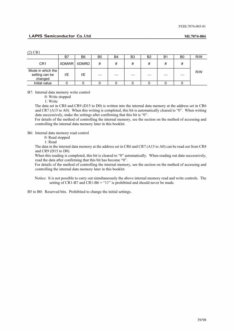
FEDL7074-003-01
ML7074-004
39/98
(2) CR1 B7 B6 B5 B4 B3 B2 B1 B0 R/W
CR1 XDMWR XDMRD # # # # # #
Mode in which the setting can be
changed I/E I/E
Initial value 0 0 0 0 0 0 0 0
R/W
B7: Internal data memory write control 0: Write stopped 1: Write
The data set in CR8 and CR9 (D15 to D0) is written into the internal data memory at the address set in CR6 and CR7 (A15 to A0). When this writing is completed, this bit is automatically cleared to “0”. When writing data successively, make the settings after confirming that this bit is “0”. For details of the method of controlling the internal memory, see the section on the method of accessing and controlling the internal data memory later in this booklet.
B6: Internal data memory read control 0: Read stopped 1: Read
The data in the internal data memory at the address set in CR6 and CR7 (A15 to A0) can be read out from CR8 and CR9 (D15 to D0). When this reading is completed, this bit is cleared to “0” automatically. When reading out data successively, read the data after confirming that this bit has become “0”. For details of the method of controlling the internal memory, see the section on the method of accessing and controlling the internal data memory later in this booklet.
Notice: It is not possible to carry out simultaneously the above internal memory read and write controls. The
setting of CR1-B7 and CR1-B6 = “11” is prohibited and should never be made. B5 to B0: Reserved bits. Prohibited to change the initial settings.
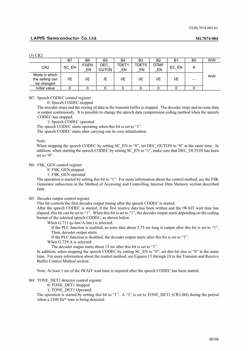
FEDL7074-003-01
ML7074-004
40/98
(3) CR2 B7 B6 B5 B4 B3 B2 B1 B0 R/W
CR2 SC_ENFGEN _EN
DEC_OUTON
TDET1_EN
TDET0_EN
DTMF_EN
EC_EN #
Mode in which the setting can
be changed I/E I/E /E I/E I/E I/E I/E
Initial value 0 0 0 0 0 0 0 0
R/W
B7: Speech CODEC control register 0: Speech CODEC stopped
The encoder stops and the storing of data in the transmit buffer is stopped. The decoder stops and no-tone data is output continuously. It is possible to change the speech data compression coding method when the speech CODEC has stopped.
1: Speech CODEC operated The speech CODEC starts operating when this bit is set to “1”. The speech CODEC starts after carrying out its own initialization.
Note: When stopping the speech CODEC by setting SC_EN to “0”, set DEC_OUTON to “0” at the same time. In addition, when starting the speech CODEC by setting SC_EN to “1”, make sure that DEC_OUTON has been set to “0”.
B6: FSK_GEN control register 0: FSK_GEN stopped 1: FSK_GEN operated
The operation is started by setting this bit to “1”. For more information about the control method, see the FSK Generator subsection in the Method of Accessing and Controlling Internal Data Memory section described later.
B5: Decoder output control register
This bit controls the first decoder output timing after the speech CODEC is started. After the speech CODEC is started, if the first receive data has been written and the tWAIT wait time has elapsed, this bit can be set to “1”. When this bit is set to “1”, the decoder output starts depending on the coding format of the selected speech CODEC, as shown below.
When G.711 (-law/A-law) is selected: If the PLC function is enabled, no-tone data about 3.75 ms long is output after this bit is set to “1”. Then, decoder output starts. If the PLC function is disabled, the decoder output starts after this bit is set to “1”.
When G.729.A is selected: The decoder output starts about 15 ms after this bit is set to “1”.
In addition, when stopping the speech CODEC by setting SC_EN to “0”, set this bit also to “0” at the same time. For more information about the control method, see Figures 15 through 18 in the Transmit and Receive Buffer Control Method section. Note: At least 1 ms of the tWAIT wait time is required after the speech CODEC has been started.
B4: TONE_DET1 detector control register 0: TONE_DET1 Stopped 1: TONE_DET1 Operated
The operation is started by setting this bit to “1”. A “1” is set to TONE_DET1 (CR3-B4) during the period when a 2100 Hz* tone is being detected.

FEDL7074-003-01
ML7074-004
41/98
B3: TONE_DET0 detector control register 0: TONE_DET0 Stopped 1: TONE_DET0 Operation
The operation is started by setting this bit to “1”. A “1” is set to TONE_DET0 (CR3-B3) during the period when a 1650 Hz* tone is being detected. Remarks: * It is possible to change the detect frequencies. Contact ROHM's responsible sales person if you wish to change these frequencies.
B2: DTMF detector control register 0: DTMF detect function stopped 1: DTMF detect function operated B1: Echo canceller control register 0: Echo canceller function stopped (The echo canceller is put in the through mode) 1: Echo canceller function active
Remarks: The operation is started after the echo canceller internal coefficients cleared.
B0: Reserved bit. Prohibited to change the initial setting.

FEDL7074-003-01
ML7074-004
42/98
(4) CR3 B7 B6 B5 B4 B3 B2 B1 B0 R/W
CR3 DSP
_ERR# #
TONE1_DET
TONE0_DET
# TX
_ERR RX
_ERR Mode in which the setting can
be changed
Initial value 0 0 0 0 0 0 0 0
R/
B7: DSP status register 0: Normal operation state 1: Abnormal operation state
This LSI has a built-in watchdog timer, and when the program of the DSP section goes into uncontrollable execution state due to external disturbances around this LSI or due to power supply abnormalities, etc., the DSP_ERR status will be set to “1” and an interrupt will be generated. When this bit becomes “1”, carry out a power down reset using either PDNB or SPDN of CR0-B7. This bit gets cleared by a power down reset operation.
Notice: The DSP_ERR status cannot detect all abnormal operation conditions. The abnormality will not be detected even when the DSP goes into uncontrolled program execution if the watchdog timer gets cleared during that program execution.
B6, B5: Reserved bit. Prohibited to change the initial setting. B4: TONE1 detector detect status register 0: Not detected 1: Detected B3: TONE0 detector detect status register 0: Not detected 1: Detected B2: Reserved bit. Prohibited to change the initial setting. B1: Transmit buffer status register 0: Transmit buffer in normal operation state 1: Transmit buffer in error state
This bit becomes “1” when an overrun error occurs in the transmit buffer, and will be “0” otherwise. B0: Receive buffer status register 0: Receive buffer in normal operation state 1: Receive buffer in error state
This bit becomes “1” when an underflow error occurs in the receive buffer, and will be “0” otherwise. An interrupt is generated whenever there is a change in the state of any of the above bits (“0” “1” or “1” “0”).

FEDL7074-003-01
ML7074-004
43/98
(5) CR4 B7 B6 B5 B4 B3 B2 B1 B0 R/W
CR4 INT DP_DET # DTMF_DET
DTMF_CODE3
DTMF_CODE2
DTMF_ CODE1
DTMF_ CODE0
Mode in which the setting can
be changed
Initial value 0 0 0 0 0 0 0 0
R/
B7: Interrupt generation status register
This is a directly coupled register with the logic of INTB inverted. A “1” will be read out from this bit when INTB is “L” and will be “0” otherwise.
0: During the period INTB is “H” 1: During the period INTB is “L”
Notice: The statuses of the INT bit and INTB may not be the same when a DSP_ERR is generated. B6: Dial pulse detector detect status register
This bit indicates the detect status of the dial pulse detector. This bit becomes “1” during the period when a dial pulse is being detected and will be “0” otherwise.
0: Dial pulse not detected 1: Dial pulse detected B5: Reserved bit. Prohibited to change the initial value.

FEDL7074-003-01
ML7074-004
44/98
B4: DTMF detector detect status register This bit indicates the detect status of the DTMF detector. This bit becomes “1” during the period when a DTMF signal is being detected and will be “0” otherwise.
0: No DTMF signal detected 1: DTMF signal detected B3 to B0: DTMF code indication registers
When DTMF_EN (CR2-B2) has been set to “1”, a valid DTMF code is stored in these bits during the period a DTMF signal is being detected (CR4-B4 DTMF_DET = “1”). These bits output the data “0000” when no DTMF signal is detected (DTMF_DET = “0”). The codes are listed in Table 5.
Table 5 DTMF detect code table
DTMF_3 DTMF_2 DTMF_1 DTMF_0Low
frequency [Hz]
High frequency
[Hz] Dial number
0 0 0 0 697 1209 1 0 0 0 1 770 1209 4 0 0 1 0 852 1209 7 0 0 1 1 941 1209 * 0 1 0 0 697 1336 2 0 1 0 1 770 1336 5 0 1 1 0 852 1336 8 0 1 1 1 941 1336 0 1 0 0 0 697 1477 3 1 0 0 1 770 1477 6 1 0 1 0 852 1477 9 1 0 1 1 941 1477 # 1 1 0 0 697 1633 A 1 1 0 1 770 1633 B 1 1 1 0 852 1633 C 1 1 1 1 941 1633 D
An interrupt is generated whenever there is a change in the statuses of the bits B6, B4 to B0 above (“0” “1” or “1” “0”).

FEDL7074-003-01
ML7074-004
45/98
(6) CR5 B7 B6 B5 B4 B3 B2 B1 B0 R/W
CR5 READY # # # # # # FGEN _FLAG
Mode in which the setting can be changed.
I/E
Initial value 0 0 0 0 0 0 0 0
R/W
B7: Initialization mode indication register 0: Other than the initialization mode 1: Initialization in progress
After the power down reset state is released, this LSI enters the initialization mode. This bit will be set to “1” in the initialization mode.
B6 to B1: Reserved bits. Prohibited to change the initial settings. B0: FSK output data setup completion flag
After writing data into the FSK output data setup register (CR18), set this bit to “1”. Once the written data is read into the internal buffer of the FSK signal generation block, this bit is automatically cleared to “0”, and an interrupt is generated at the same time. Do not write to CR5 when this bit is “0”.
An interrupt is generated when there is a change in bit B0 (“1” “0”).

FEDL7074-003-01
ML7074-004
46/98
(7) CR6 B7 B6 B5 B4 B3 B2 B1 B0 R/W
CR6 A15 A14 A13 A12 A11 A10 A9 A8
Mode in which the value can be
changed I/E
Initial value 0 0 0 0 0 0 0 0
/W
B7 to B0: Higher order address of the internal data memory
These bits are the registers for setting the higher order byte of the address in the internal data memory. For details on the method of writing, see the section on the method of accessing and controlling the internal data memory
(8) CR7
B7 B6 B5 B4 B3 B2 B1 B0 R/W
CR7 A7 A6 A5 A4 A3 A2 A1 A0
Mode in which the value can be
changed I/E
Initial value 0 0 0 0 0 0 0 0
/W
B7 to B0: Lower order address of the internal data memory
These bits are the registers for setting the lower order byte of the address in the internal data memory. For details on the method of writing, see the section on the method of accessing and controlling the internal data memory.
(9) CR8
B7 B6 B5 B4 B3 B2 B1 B0 R/W
CR8 D15 D14 D13 D12 D11 D10 D9 D8
Mode in which the value can be
changed I/E
Initial value 0 0 0 0 0 0 0 0
R/W
B7 to B0: Higher order data of the internal data memory
These bits are the registers for setting the higher order byte of the data in the internal data memory. For details on the method of writing and reading, see the section on the method of accessing and controlling the internal data memory.
(10) CR9
B7 B6 B5 B4 B3 B2 B1 B0 R/W
CR9 D7 D6 D5 D4 D3 D2 D1 D0
Mode in which the value can be
changed I/E
Initial value 0 0 0 0 0 0 0 0
R/W
B7 to B0: Lower order data of the internal data memory
These bits are the registers for setting the lower order byte of the data in the internal memory. For details on the method of writing and reading, see the section on the method of accessing and controlling the internal data memory.

FEDL7074-003-01
ML7074-004
47/98
(11) CR10 B7 B6 B5 B4 B3 B2 B1 B0 R/W
CR10 # DPDET_
EN #
TDET1_SEL
TDET0_SEL
VFRO1_SEL
VFRO0 _SEL
AIN _SEL
Mode in which the value can be
changed I/E I/ I/ I/E I/E I/E
Initial value 0 0 0 0 0 0 0 0
R/W
B7: Reserved bit. Prohibited to change the initial setting. B6: Dial pulse detector control register 0: Dial pulse detector stopped 1: Dial pulse detector active B5: Reserved bit. Prohibited to change the initial setting. B4: TDET1 detect path select register 0: Transmitting section 1: Receiving section B3: TDET0 detect path select register 0: Transmitting section 1: Receiving section B2: VFRO1 selection 0: AVREF (Output of about 1.4 V) 1: Receiver side speech output B1: VFRO0 selection 0: AVREF (Output of about 1.4 V) 1: Receiver side speech output B0: Input amplifier selection 0: Selection of AMP0 1: Selection of AMP1

FEDL7074-003-01
ML7074-004
48/98
(12) CR11 B7 B6 B5 B4 B3 B2 B1 B0 R/W
CR11 FRAME/
DMA 10ms /20ms
16B /8B
# # SC
_SEL1SC
_SEL0 G711_
PLCDIS Mode in which
the value can be changed
I/ I/ I/ I/E I/E I/E
Initial value 0 0 0 0 0 0 0 0
R/W
B7: FRAME/DMA select register 0: FRAME access 1: DMA slave interface access
This bit selects the method of accessing the transmit and receive buffers. The initial value is frame access. B6: 10 ms/20 ms select register 0: 10 ms 1: 20 ms
This bit selects the buffering time of the transmit and receive buffers. The initial value is 10 ms. B5: MCU interface data width select register 0: 16-bit data width interface 1: 8-bit data width interface
This bit selects the width of the data bus connected to the transmit and receive buffers. The initial value is 16 bits. When the 8-bit bus width is used, tie D15 to D8 to either “1” or “0”.
B4, B3: Reserved bits. Prohibited to change the initial values. B2, B1: Speech CODEC select registers
- When using the analog I/F mode, (0, 0): G.729.A (0, 1): G.711 (-law) (1, 0): Prohibited (1, 1): G.711 (A-law)
The speech CODEC can be selected when CR2-B7 (SC_EN) is in the “0” state. Prohibited to change the speech CODEC when it is operating. - When using the PCM I/F mode (CR12-B0 = “1”), These bits select the PCM I/F coding method. Further, the speech CODEC select bits will be CR12-B2 and CR12-B1.
(0, 0): 16-bit linear (2’s complement format) (0, 1): G.711 (-law) (1, 0): Prohibited (1, 1): G.711 (A-law)
The coding method can be selected when CR2-B7 (SC_EN) is in the “0” state. Prohibited to change the coding method during operation.
B0: G.711 PLC function disable control register
Setting this bit to “1” disables the G.711 PLC function. If the G.711 PLC function is disabled, no-tone data is output when a receive error occurs.
0: Enable 1: Disable
This bit can be enabled or disabled when CR2-B7 (SC_EN) is “0”. Change of setting during operation is prohibited.

FEDL7074-003-01
ML7074-004
49/98
(13) CR12 B7 B6 B5 B4 B3 B2 B1 B0 R/W
CR12 # # # # # PSC
_SEL1PSC
_SEL0 PCMIF
_EN Mode in which
the value can be changed
I/E I/E I/
Initial value 0 0 0 0 0 0 0 0
/W
B7 to B3: Reserved bits. Prohibited to change the initial settings. B2, B1: Speech CODEC select registers in the PCM I/F mode (0, 0): G.729.A (0, 1): G.711 (-law) (1, 0): Prohibited (1, 1): G.711 (A-law)
The speech CODEC type can be selected when CR2-B7 (SC_EN) is in the “0” state. Prohibited to change the speech CODEC type during operation.
B0: PCM I/F mode control register 0: Analog I/F mode
Set the speech CODEC type selection in CR11-B2 and CR11-B1. 1: PCM I/F mode
Set the PCM/IF coding method in CR11-B2 and CR11-B1, and set the speech CODEC type selection in B2 and B1 of this register.
(14) CR13
B7 B6 B5 B4 B3 B2 B1 B0 R/W
CR13 $ $ $ $ $ $ $ $
Mode in which the value can be
changed
Initial value
/
B7 to B0: Reserved bits. Prohibited to change the initial settings. (15) CR14
B7 B6 B5 B4 B3 B2 B1 B0 R/W
CR14 $ $ $ $ $ $ $ $
Mode in which the value can be
changed
Initial value
/
B7 to B0: Reserved bits. Prohibited to change the initial settings.

FEDL7074-003-01
ML7074-004
50/98
(16) CR15 B7 B6 B5 B4 B3 B2 B1 B0 R/W
CR15 TA2 TA1 TA0 $ $ $ $ $
Mode in which the value can be
changed I/ I/ I/
Initial value 0 0 0 0 0 0 0 0
R/W
B7 to B5: Registers for adjustment
Set to “010” at the beginning of the initialization mode. (0, 1, 0): Fixed
B4 to B0: Reserved bits. Prohibited to change the initial settings. (17) CR16
B7 B6 B5 B4 B3 B2 B1 B0 R/W
CR16 # # # # # # GPI1 GPI0
Mode in which the value can be
changed
Initial value 0 0 0 0 0 0
R/
B7 to B2: Reserved bits. Prohibited to change the initial settings. B1: GPI1 level read out register 0: GPI1 level is “0”. 1: GPI1 level is “1”. B0: GPI0 level read out register 0: GPI0 level is “0”. 1: GPI0 level is “1”.
Note: GPI0 is used as the input of the dial pulse detector in the secondary functions. It is possible to read out GPI0 even when the dial pulse detector is operating.

FEDL7074-003-01
ML7074-004
51/98
(18) CR17 B7 B6 B5 B4 B3 B2 B1 B0 R/W
CR17 # # # # # # GPO1 GPO0
Mode in which the value can be
changed I/E I/E
Initial value 0 0 0 0 0 0 0 0
R/W
B7 to B2: Reserved bits. Prohibited to change the initial settings. B1: GPO1 output level register 0: “L” level is output at GPO1. 1: “H” level is output at GPO1. B0: GPO0 output level register 0: “L” level is output at GPO0. 1: “H” level is output at GPO0.
Notice: GPO0 is used in the secondary functions as the output of the dial pulse transmitter. Note that it is prohibited to change the content of the GPO0 bit when the dial pulse detector is operating.
(19) CR18
B7 B6 B5 B4 B3 B2 B1 B0 R/W
CR18 FGEN_D7
FGEN _D6
FGEN_D5
FGEN_D4
FGEN_D3
FGEN_D2
FGEN _D1
FGEN _D0
Mode in which the value can be
changed I/E
Initial value 0 0 0 0 0 0 0 0
R/W
B7 to B0: FSK transmit data setting registers
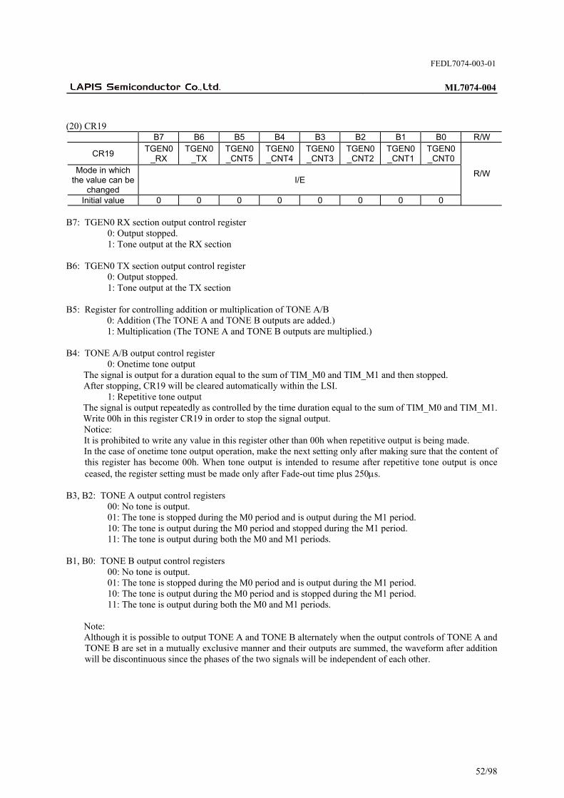
FEDL7074-003-01
ML7074-004
52/98
(20) CR19 B7 B6 B5 B4 B3 B2 B1 B0 R/W
CR19 TGEN0
_RX TGEN0
_TX TGEN0_CNT5
TGEN0_CNT4
TGEN0_CNT3
TGEN0_CNT2
TGEN0 _CNT1
TGEN0 _CNT0
Mode in which the value can be
changed I/E
Initial value 0 0 0 0 0 0 0 0
R/W
B7: TGEN0 RX section output control register 0: Output stopped. 1: Tone output at the RX section B6: TGEN0 TX section output control register 0: Output stopped. 1: Tone output at the TX section B5: Register for controlling addition or multiplication of TONE A/B 0: Addition (The TONE A and TONE B outputs are added.) 1: Multiplication (The TONE A and TONE B outputs are multiplied.) B4: TONE A/B output control register 0: Onetime tone output
The signal is output for a duration equal to the sum of TIM_M0 and TIM_M1 and then stopped. After stopping, CR19 will be cleared automatically within the LSI.
1: Repetitive tone output The signal is output repeatedly as controlled by the time duration equal to the sum of TIM_M0 and TIM_M1. Write 00h in this register CR19 in order to stop the signal output. Notice: It is prohibited to write any value in this register other than 00h when repetitive output is being made. In the case of onetime tone output operation, make the next setting only after making sure that the content of this register has become 00h. When tone output is intended to resume after repetitive tone output is once ceased, the register setting must be made only after Fade-out time plus 250s.
B3, B2: TONE A output control registers 00: No tone is output. 01: The tone is stopped during the M0 period and is output during the M1 period. 10: The tone is output during the M0 period and stopped during the M1 period. 11: The tone is output during both the M0 and M1 periods. B1, B0: TONE B output control registers 00: No tone is output. 01: The tone is stopped during the M0 period and is output during the M1 period. 10: The tone is output during the M0 period and is stopped during the M1 period. 11: The tone is output during both the M0 and M1 periods.
Note: Although it is possible to output TONE A and TONE B alternately when the output controls of TONE A and TONE B are set in a mutually exclusive manner and their outputs are summed, the waveform after addition will be discontinuous since the phases of the two signals will be independent of each other.

FEDL7074-003-01
ML7074-004
53/98
(21) CR20 B7 B6 B5 B4 B3 B2 B1 B0 R/W
CR20 TGEN1
_RX TGEN1
_TX TGEN1_CNT5
TGEN1_CNT4
TGEN1_CNT3
TGEN1_CNT2
TGEN1 _CNT1
TGEN1 _CNT0
Mode in which the value can be
changed I/E
Initial value 0 0 0 0 0 0 0 0
R/W
B7: TGEN1 PCM section output control register 0: Output stopped. 1: Tone output at the RX section B6: TGEN1 TX section output control register 0: Output stopped. 1: Tone output at the TX section B5: Register for controlling addition or multiplication of TONE C/D 0: Addition (The TONE C and TONE D outputs are added.) 1: Multiplication (The TONE C and TONE D outputs are multiplied.) B4: TONE C/D output control register 0: Onetime tone output
The signal is output for a duration equal to the sum of TIM_M0 and TIM_M1 and then stopped. After stopping, CR20 will be cleared automatically within the LSI.
1: Repetitive tone output The signal is output repeatedly as controlled by the time duration equal to the sum of TIM_M0 and TIM_M1. Write 00h in this register CR20 in order to stop the signal output. Notice: It is prohibited to write any value in this register other than 00h when repetitive output is being made. In the case of onetime tone output operation, make the next setting only after making sure that the content of this register has become 00h. When tone output is intended to resume after repetitive tone output is once ceased, the register setting must be made only after Fade-out time plus 250s.
B3, B2: TONE C output control registers 00: No tone is output. 01: The tone is stopped during the M0 period and is output during the M1 period. 10: The tone is output during the M0 period and stopped during the M1 period. 11: The tone is output during both the M0 and M1 periods. B1, B0: TONE D output control registers 00: No tone is output. 01: The tone is stopped during the M0 period and is output during the M1 period. 10: The tone is output during the M0 period and is stopped during the M1 period. 11: The tone is output during both the M0 and M1 periods.
Note: Although it is possible to output TONE C and TONE D alternately when the output controls of TONE C and TONE D are set in a mutually exclusive manner and their outputs are summed, the waveform after addition will be discontinuous since the phases of the two signals will be independent of each other.

FEDL7074-003-01
ML7074-004
54/98
Figure 25 shows block diagrams of the tone generation blocks (TONE_GEN0, TONE_GEN1). There is no difference in the tone generation method between TONE_GEN0 and TONE_GEN1. So, using TONE_GEN0 as an example, Figure 26 shows the tone output control method, and Figures 27 and 28 show the tone output control parameters.
TGEN0_FREQ_A
TONE_A
TGEN0_GAIN_A
TGEN0_GAIN_B
TGEN0_TXGAIN_TOTAL
CR19-B5TGEN0_FREQ_B
TONE_BTGEN0_RXGAIN_TOTAL
TX
RX
[TONE_GEN0]
TGEN1_FREQ_C
TONE_C
TGEN1_GAIN_C
TGEN1_GAIN_D
TGEN1_TXGAIN_TOTAL
CR20-B5TGEN1_FREQ_D
TONE_DTGEN1_RXGAIN_TOTAL
TX
RX
[TONE_GEN1]
Fig. 25 Tone generator section block diagram

FEDL7074-003-01
ML7074-004
55/98
TONE A, B frequency setting
FADE control setting(Common to TONE A and
TONE B)
TONE A/B/TOTAL gain setting
CR19=xxx0xxxxb
CR19 is cleared automaticallywithin the LSI
CR19=00000000b
Onetime tone output method
TONE A, B frequency setting
FADE control setting(Common to TONE A and
TONE B)
TONE A/B/TOTAL gain setting
CR19=xxx1xxxxb
Set CR19=00000000b
Repetitive tone output method
Tone output stops
Repetitive output oftone
Stopping afteronetime tone output
TONE A/B M0/M1 outputcontrol setting
TONE A/B M0/M1 outputcontrol setting
Fade-in step setting(common to Tone A and
Tone B)
Fade-out step setting(common to Tone A and
Tone B)
Fade-out time setting(common to Tone A and
Tone B)
Fade-in step setting(common to Tone A and
Tone B)
Fade-out step setting(common to Tone A and
Tone B)
Fade-out time setting(common to Tone A and
Tone B)
"1""0" "1""0"
* When tone output is intended to resume afterrepetitive tone output is once ceased, the registersetting must be made only after Fade-out timeplus 250s.
M0/M1 Output duration setting(Common to TONE A and
TONE B)
M0/M1 Output duration setting(Common to TONE A and
TONE B)
Fig. 26 Tone output control method (in the case of TONE_GEN0)

FEDL7074-003-01
ML7074-004
56/98
TIM-M0 TIM-M1
FREQ
GAIN
M0 ON M1 ON
Onetim toneoutput
Repetitive toneoutput
Output is made by repeating onetime tone output settings
GAIN
TIM-M0 TIM-M1
FREQ
M0 OFF M1 ON
TIM-M0 TIM-M1
M0 OFF M1 ON
TIM-M0 TIM-M1
FREQ
M0 ON M1 OFF
TIM-M0 TIM-M1
FREQ
M0 OFF M1 ON
Fig. 27 Tone output control parameters (in the case of TONE_GENO/TGEN0_FADE_CONT OFF)

FEDL7074-003-01
ML7074-004
57/98
Fig. 28 Tone output control parameters (in the case of TONE_GENO/TGEN0_FADE_CONT “ON”)
TIM_M0 TIM_M1
GAIN
M0 ON M1 ON
Onetime ToneOutput
RepetitiveTone Output
GAIN
M0 OFF M1 ON M0 OFF M1 ON
M0 ON M1 OFF
M0 OFF M1 ON
Outputs a set of onetime tone output repetitively(TONE_A and TONE_B are output alternately.)
GAIN_A
M0 ON M1 ON M0 ON M1 ON
TONE_A TONE_B TONE_A TONE_B
GAIN_B
TIM_M0 TIM_M1TIM_M0 TIM_M1
F-i F-o
F-i F-o
F-i F-o
F-i F-o F-i F-o
F-i F-oF-i F-o F-i F-o F-i F-o
* "F-i" and "F-o" are times to fade in and to fadeout respectively. Parameters to determine themwill be discussed later in this document..
Outputs a set of onetime tone output repetitively(CR19="00h" is set in a way)
GAIN
M0 OFF M1 ON M0 OFF M1 ON
F-i F-o F-i F-o
Outputs a set of onetime tone outputrepetitively
CR19="00h"

FEDL7074-003-01
ML7074-004
58/98
METHOD OF ACCESSING AND CONTROLLING INTERNAL DATA MEMORY Writing Method The four 8-bit registers CR6 to CR9 mapped within the set of control registers are allocated to the following: 16-bit address of the internal data memory (A15 to A0) 16-bit data to be written (D15 to D0) The initialization mode is entered and a “1” is set in CR5-B7 (READY) about 1.0 s after release from a power down reset due to PDNB or after a release from a software power down reset due to CR0-B7. In this writable state, after setting in CR6 to CR9 the internal data memory address and the data to be written, if a “1” is set in CR1-B7 (XDMWR), the writing of one word of data in the internal data memory will be completed. After completion of writing the data, CR1-B7 will be cleared to “0” automatically. The method of setting data in the internal data memory is shown in Fig. 29. Repeat the above operations for writing to several memory locations. When all the writing operations have been completed, the normal operations can be started by setting a “1” in CR0-B0 (OPE_STAT). It is possible to re-write even in modes other than the initialization mode the internal data memory locations related to gain control, TONE transmission, EC, DPGEN, and TIMER. Even in such cases, carry out the updating of the internal data memory using the same method as described above. Table 6 to Table 9 list the internal data memory and related control registers. Note: When data is set in the internal data memory during operation, since the reading is done in synchronization with the SYNC signal (8 kHz), maintain the state for 250 s or more.
Fig. 29 Method of setting data in the internal data memory
CR8 (Internal memory higher data)
YES
NOCR1-B7, B6 = 0
Updating internal memoryCR1-B7 cleared automatically
External setting
Automatic processing inside the LSI
CR9 (Internal memory lower data)
CR7 (Internal memory lower address)
CR6 (Internal memory higher address)
CR1-B7(XDMWR) = 1
Time duration from setting of CR1-B7until it is cleared. In initialization mode: 20 s max. In normal operation: 250 s max.
Start writing

FEDL7074-003-01
ML7074-004
59/98
Reading Method After setting the internal data memory address in CR6 and CR7, one word of data from the internal data memory is stored in CR8 and CR9 when a “1” is written in CR1-B6 (XDMRD). After reading the data, CR1-B6 will be cleared to “0” automatically. The method of reading the internal data memory is shown in Fig. 30. Further, the internal data memory read out can only be made for the internal data memory and the read only data memory within the related registers listed in Table 6 to Table 9. Notice: When the internal data memory is read out during operation, since the reading out is done in synchronization with the SYNC signal (8 kHz), maintain the set address in the same state for 250 s or more.
Fig. 30 Method of reading out internal data memory
CR1-B6(XDMRD) = 1
YES
NOCR1-B6(XDMRD) = 0
External setting and read out
CR8 (Internal memory higher data) read out
CR7 (Internal memory lower address)
CR6 (Internal memory higher address)
Time duration from setting of CR1-B7until it is cleared: In initialization mode: 20 s max. In normal operation: 250 s max.
Start read out
CR9 (Internal memory lower data) read out
Cleared automatically to "0" after theread out data is stored in CR8 andCR9.
YES
NOCR1-B7, B6 = 0

FEDL7074-003-01
ML7074-004
60/98
Table 6 Internal data memory and related control registers (1/4)
Initial value Modes in which updating and
read are possible Function
name Internal data memory name Address
Data Data value
In initializa-
tion mode
During idle
state
During operation
Transmit gain (TXGAIN) 02ACh 0080h 0 dB Y Y Y Receive gain (RXGAIN) 02ADh 0080h 0 dB Y Y Y Side tone gain (STGAIN) 02AEh 0000h MUTE Y Y Y Gain fade control (GAIN_FADE_CONT)
02AFh 0000h disabled Y Y N
Gain fade-in step (GAIN_FADE_IN_ST)
02B0h 4C10h +1.5dB Y Y*1 N
Gain control
Gain fade-out step (GAIN_FADE_OUT_ST)
02B1h 35D9h -1.5dB Y Y*1 N
TGEN0 transmit control CR19 00h
Transmission stopped
Y Y Y
TGEN0 in-execution flag (TGEN0_EXE_FLAG) (Read-only memory)
1141h 0000h Not in
execution Y Y Y
TONE A frequency control (TGEN0_FREQ_A)
1143h 0CCCh 400 Hz Y Y N
TONE B frequency control (TGEN0_ FREQ_B)
1145h 007Ah 15 Hz Y Y N
TONE A gain control (TGEN0_GAIN_A) 1147h 0080h –13.3 dBm0 Y Y Y TONE B gain control (TGEN0_GAIN_B) 1148h 0080h –13.3 dBm0 Y Y Y TGEN0 time control 0 (TGEN0_TIM_M0) 1149h 0FA0h 500 ms Y Y N TGEN0 time control 1 (TGEN0_TIM_M1) 114Ch 0FA0h 500 ms Y Y N TGEN0 RX section tone total gain (TGEN0_RXGAIN_TOTAL)
1150h 0080h 0 dB Y Y Y
TGEN0 TX section tone total gain (TGEN0_TXGAIN_TOTAL)
1151h 0080h 0 dB Y Y Y
TGEN0 fade control (TGEN0_FADE_CONT)
113Bh 0000h disabled Y Y N
TGEN0 fade-in step (TGEN0_FADE_IN_ST)
113Ch 47CFh +1dB Y Y N
TGEN0 fade-out step (TGEN0_FADE_OUT_ST)
113Dh 390Ah -1dB Y Y N
TGEN0 fade-out time (TONE0_FADE_OUT_TIM)
113Eh 002Bh 43 Sync Y Y N
TGEN0 total gain fade control (TGEN0_GAIN_TOTAL_FADE_CONT)
114Dh 0000h disabled Y Y N
TGEN0 total gain fade-in step (TGEN0_GAIN_TOTAL_FADE_IN_ST)
114Eh 4C10h +1.5dB Y Y N
Tone genera- tion 0 TONE_ GEN0
TGEN0 total gain fade-out step (TGEN0_GAIN_TOTAL_FADE_OUT_ST)
114Fh 35D9h -1.5dB Y Y N
*1 when gain fade is disabled

FEDL7074-003-01
ML7074-004
61/98
Table 7 Internal data memory and related control registers (2/4)
Initial value Modes in which updating and
read are possible Function
name Internal data memory name Address
Data Data value
In initializa-
tion mode
During idle
state
During operation
TGEN1 transmit control CR20 00h
Transmission stopped
Y Y Y
TGEN1 in-execution flag (TGEN1_EXE_FLAG) (Read-only memory)
1158h 0000h Not in
execution Y Y Y
TONE C frequency control (TGEN1_FREQ_C)
115Ah 0CCCh 400 Hz Y Y N
TONE D frequency control (TGEN1_ FREQ_D)
115Ch 007Ah 15 Hz Y Y N
TONE C gain control (TGEN1_GAIN_C) 115Eh 0080h –13.3 dBm0 Y Y Y TONE D gain control (TGEN1_GAIN_D) 115Fh 0080h –13.3 dBm0 Y Y Y TGEN1 time control 0 (TGEN1_TIM_M0) 1160h 0FA0h 500 ms Y Y N TGEN1 time control 1 (TGEN1_TIM_M1) 1163h 0FA0h 500 ms Y Y N TGEN1 RX section tone total gain (TGEN1_RXGAIN_TOTAL)
1167h 0080h 0 dB Y Y Y
TGEN1 TX section tone total gain (TGEN1_TXGAIN_TOTAL)
1168h 0080h 0 dB Y Y Y
TGEN1 fade control (TGEN1_FADE_CONT)
1152h 0000h Stopped Y Y N
TGEN1 fade-in step (TGEN1_FADE_IN_ST)
1153h 47CFh +1dB Y Y N
TGEN1 fade-out step (TGEN1_FADE_OUT_ST)
1154h 390Ah -1dB Y Y N
TGEN1 fade-out time (TONE1_FADE_OUT_TIM)
1155h 002Bh 43 Sync Y Y N
TGEN1 total gain fade control (TGEN1_GAIN_TOTAL_FADE_CONT)
1164h 0000h Stopped Y Y N
TGEN1 total gain fade-in step (TGEN1_GAIN_TOTAL_FADE_IN_ST)
1165h 4C10h +1.5dB Y Y N
Tone genera- tion 1 TONE_ GEN1
TGEN1 total gain fade-out step (TGEN1_GAIN_TOTAL_FADE_OUT_ST)
1166h 35D9h -1.5dB Y Y N
FSK output control (FGEN_EN) CR2-B6 0b Stopped Y Y Y FSK output data setting complete flag (FGEN_FLAG)
CR5-B0 0b Writable Y Y Y
FSK output data setting register (FGEN_D[7:0])
CR18 00h 00h Y Y Y
FSK generator
FSK_ GEN
FSK gain control (FGEN_GAIN) 02C4h 0080h –13.3 dBm0 Y Y N

FEDL7074-003-01
ML7074-004
62/98
Table 8 Internal data memory and related control registers (3/4)
Initial value Modes in which updating and
read are possible Function
name Internal data memory name Address
Data Data value
In initializa-
tion mode
During idle
state
During operation
TONE 0 control (TDET0_EN) CR2-B3 0b Stopped Y Y Y Main signal detect level control (TDET0_S_TH)
1356h 1EBBh –5.3 dBm0 Y Y N
Noise detect level control (TDET0_N_TH)
136Bh 1EBBh –5.3 dBm0 Y Y N
Detect ON guard timer control (TDET0_ON_TM)
136Ch 0028h 5 ms Y Y N
Detect OFF guard timer control (TDET0_OFF_TM)
136Dh 0028h 5 ms Y Y N
TONE 0 detector
TONE_ DET0
Detect frequency (TDET0_FREQ) - - - - h - 1650 Hz Y N N TONE 1 control (TDET1_EN) CR2-B4 0b Stopped Y Y Y Main signal detect level control (TDET1_S_TH)
1382h 1EBBh –5.3 dBm0 Y Y N
Noise detect level control (TDET1_N_TH)
1397h 1EBBh –5.3 dBm0 Y Y N
Detect ON guard timer control (TDET1_ON_TM)
1398h 0028h 5 ms Y Y N
Detect OFF guard timer control (TDET1_OFF_TM)
1399h 0028h 5 ms Y Y N
TONE 1 detector
TONE_ DET1
Detect frequency (TDET1_FREQ) - - - - h - 2100 Hz Y N N DTMF control (DTMF_EN) CR2-B2 0b Stopped Y Y Y Detect level control (DTMF_TH) 0170h 1000h –37.0 dBm0 Y Y N Detect ON guard timer control (DTMF_ON_TM) 01D5h 00A0h 20 ms Y Y N
Detect OFF guard timer control (DTMF_OFF_TM) 01D7h 00A0h 20 ms Y Y N
DTMF detector
DTMF_
REC Noise detect function control (DTMF_NDET_CONT)
01D8h 0002h Enabled Y Y N
EC control (EC_EN) CR2-B1 0b Stopped Y Y Y EC control (EC_CR) 002Ch 0012h HD ATT OFF Y Y Y
Echo canceller
GLPAD control (GLPAD_CR) 002Dh 000Fh +6/–6 dB Y Y N Dial pulse detect control (DPDET_EN) CR10-B6 0b Stopped Y Y Y Detect ON guard timer control (DPDET_ON_TIM)
0FCBh 0028h 5 ms Y Y N
Detect OFF guard timer control (DPDET_OFF_TIM)
0FCCh 0028h 5 ms Y Y N
Detect polarity control (DPDET_POL) 0FCAh 0000h Positive logic Y Y N End of detect timer control (DPDET_DETOFF_TIM)
0FD1h 03E8h 125 ms Y Y N
Dial pulse detector
DPDET
Detect code (DPDET_CODE) (Read only data memory)
0FD3h 0000h Not detected Y Y Y
Dial pulse output control (DPGEN_EN) (Can be read out)
0FBDh 0000h Stopped Y Y Y
Pulse count setting (DPGEN_DATA) 0FBEh 0000h Stopped Y Y N Dial pulse speed control (DPGEN_PPS) 0FBFh 0000h 10 pps Y Y N Dial pulse make ratio control (DPGEN_DUTY) 0FC0h 0108h 33 ms Y Y N
End of output control (DPGEN_OFF_TIM) 0FC2h 03E8h 125 ms Y Y N
Dial Pulse generator
DPGEN
Output polarity control (DPGEN_POL) 0FC3h 0000h Positive logic Y Y N

FEDL7074-003-01
ML7074-004
63/98
Table 9 Internal data memory and related control registers (4/4)
Initial value Modes in which updating and
read are possible Function
name Internal data memory name Address
Data Data value
In initializa-
tion mode
During idle
state
During operation
Timer control (TIM_EN) 0FB7h 0000h Stopped Y Y Y Timer counter value display (TIM_COUNT) (read only data memory)
0FB8h 0000hCount value
0000h Y Y Y TIMER
Timer data setting (TIM_DATA) 0FB9h FFFFh MAX FFFFh Y Y N Outband control
Outband control (OUTBAND_CONTROL) 0FDAh 0000h Stopped Y N N
Outband G.729.A
data
Outband G.729.A data (OUTBAND_G729_DAT)
00A6h00A7h00A8h00A9h00AAh
7852h80A0h00FAhC200h07D6h
Y N N
Version LSI code display (ML7074_VERSION) (read only data memory) 0152h 0003h ML7074-004 Y Y Y
Note: Initialization mode: The state after release from a power down reset, and in which the initial values of control registers and internal data memory can be altered. During idle state: The state in which the function given in the function name column has stopped. During operation: The state in which the function given in the function name column is operating.

FEDL7074-003-01
ML7074-004
64/98
Gain Control (TXGAIN, RXGAIN, STGAIN) It is possible to change the values of the transmit gain (TXGAIN), receive gain (RXGAIN), and side tone gain (STGAIN). The positions of the respective gain controllers are the following.
Transmit gain (TXGAIN): Immediately before the speech CODEC input. Receive gain (RXGAIN): Immediately after the speech CODEC output. Side tone gain (STGAIN): Added to the input of the receiver section LPF from the output of the
transmitter section BPF of the linear PCM CODEC. A. Internal data memory for adjusting transmit gain (TXGAIN)
Initial value: 0080h (0.0 dB) When changing the gain value, compute it using the following equation: Equation: 0080h GAIN Example: Making the gain +6 dB (2): 0080h 2 = 0100h
Upper limit : About 40 dB higher (data: 3200h) : 0 dB (data: 0080h) Lower limit : About –42 dB (data: 0001h) : MUTE (data: 0000h)
B. Internal data memory for adjusting receive gain (RXGAIN)
Initial value: 0080h (0.0 dB) When changing the gain value, compute it using the following equation: Equation: 0080h GAIN Example: Making the gain +6 dB (2): 0080h 2 = 0100h
Upper limit : About 40 dB higher (data: 3200h) : 0 dB (data: 0080h) Lower limit : About –42 dB (data: 0001h) : MUTE (data: 0000h)
C. Internal data memory for adjusting side tone gain (STGAIN)
Initial value: 0000h (MUTE) When changing the side tone gain value, compute it using the following equation: Equation: 1000h GAIN Example: Making the gain –20 dB (0.1): 1000h 0.1 = 019Ah
Upper limit : 0 dB (data: 1000h) Lower limit : About –72 dB (data: 0001h) : MUTE (data: 0000h)

FEDL7074-003-01
ML7074-004
65/98
D. Internal data memory for gain fade (GAIN_FADE_CONT) “1” in B0 enables fade-in/-out in Tx gain alternation; “1” in B1 enables the function in Rx gain alternation; and “1” in B2 enables the function at muting in outband control.
B7 B6 B5 B4 B3 B2 B1 B0
OUTBAND_FADE_ CONT
RX_FADE_CONT
TX_FADE_CONT
Initial value
0 0 0 0 0 0 0 0
Initial value : 0000h (Outband : disabled, Rx : disabled, Tx : disabled)
B7, 6, 5, 4, 3 : Reserved bits (Prohibited to change the initial settings) B2 : OUTBAND_FADE_CONT 1 : ON (Fading-in/-out at muting and at un-muting) 0 : OFF B1 : RX_FADE_CONT 1 : ON (Fading-in/-out at Rx gain alternation) 0 : OFF B0 : TX_FADE_CONT 1 : ON (Fading-in/-out at Tx gain alternation) 0 : OFF
E. Internal data memory for gain fade-in step (GAIN_FADE_IN_ST)
Initial value: 4C10h (+1.5dB) When changing the step value, X, compute it using the following equation: Equation: 10^(X/20)*16384 Example: Making the step value +3 dB: 10^(3/20)*16384 = 23143d = 5A67h
Upper limit : About +6.0 dB (data: 7FFFh) Lower limit : About +0.1 dB (data: 40BDh)
F. Internal data memory forgain fade-out step (GAIN_FADE_OUT_ST)
Initial value: 35D9h (-1.5dB) When changing the step value, X, compute it using the following equation: Equation: 10^(X/20)*16384 Example: Making the step value -3 dB: 10^(-3/20)*16384 = 11598d = 2D4Eh
Upper limit : About -6.0 dB (data: 2000h) Lower limit : About -0.1 dB (data: 3F44h)
(Note) Step values for fade-in and fade-out can be determined independently; whereas the step values determined for fade-in and fade-out are common to Tx gain, Rx gain and OUTBAND_FADE_CONT.

FEDL7074-003-01
ML7074-004
66/98
Tone Generator0 (TONE_GEN0) It is possible to set the various types of parameters of the tone generator block. A. Internal data memory for tone frequency control
TONE_A (TGEN0_FREQ_A) Initial value: 0CCCh (400 Hz) TONE_B (TGEN0_FREQ_B) Initial value: 007Ah (15 Hz)
At the initial setting values a TONE A of 400 Hz and a TONE B of 15 Hz are output. Use the following equation to compute the value of the setting when changing the frequency. Equation: A 8.192 (A is the frequency to be set) Example: To set a frequency of 2100 Hz: 2100 8.192 4333h Upper limit : 3 kHz (data: 6000h) Lower limit : 15 Hz (data: 007Ah)
B. Internal data memory for tone gain control
TONE_A (TGEN0_GAIN_A) Initial value: 0080h TONE_B (TGEN0_GAIN_B) Initial value: 0080h The output level with the initial setting will be –13.3 dBm0. Use the following equation to compute the value of the setting when changing the gain. Equation: 0080h GAIN Example: For reducing the gain by 6 dB (0.5): 0080h 0.5 = 0040h Upper limit : 12 dB more (data: 01FDh) Lower limit : –12 dB less (data: 0020h)
Notice: Make sure that the maximum amplitude does not exceed 3.17 dBm0 when the tones are multiplied or added.
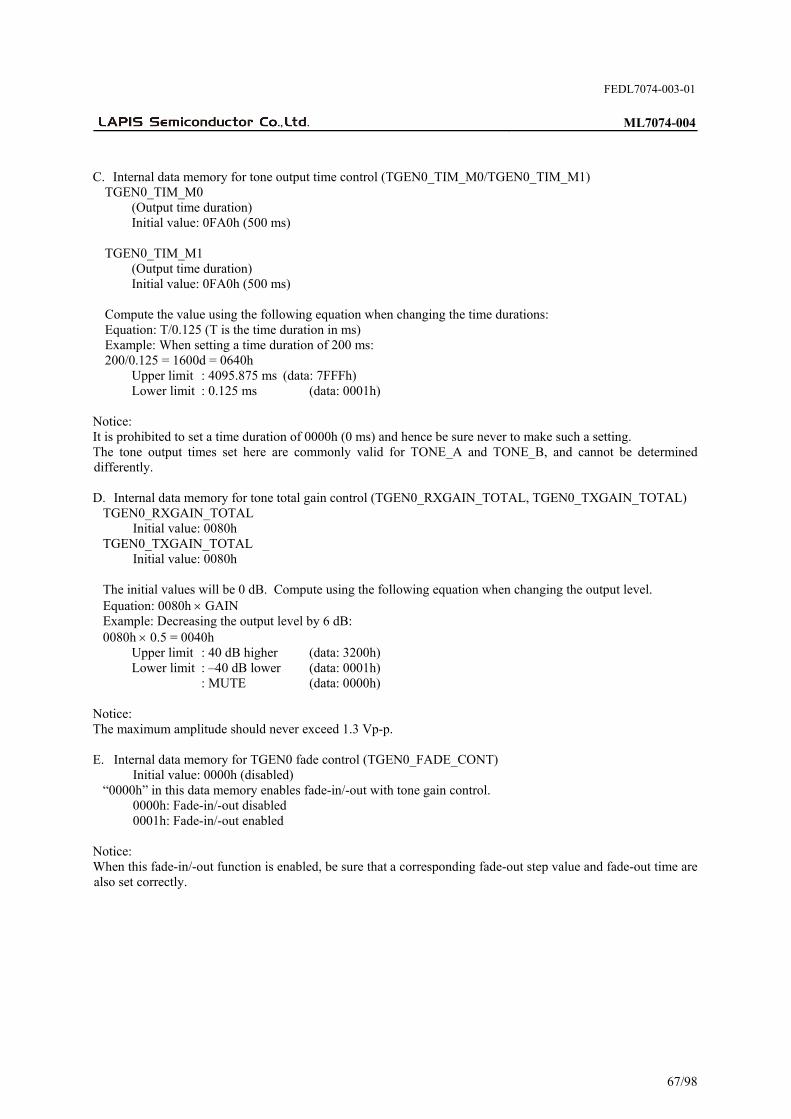
FEDL7074-003-01
ML7074-004
67/98
C. Internal data memory for tone output time control (TGEN0_TIM_M0/TGEN0_TIM_M1) TGEN0_TIM_M0 (Output time duration) Initial value: 0FA0h (500 ms) TGEN0_TIM_M1 (Output time duration) Initial value: 0FA0h (500 ms) Compute the value using the following equation when changing the time durations: Equation: T/0.125 (T is the time duration in ms) Example: When setting a time duration of 200 ms: 200/0.125 = 1600d = 0640h
Upper limit : 4095.875 ms (data: 7FFFh) Lower limit : 0.125 ms (data: 0001h)
Notice: It is prohibited to set a time duration of 0000h (0 ms) and hence be sure never to make such a setting. The tone output times set here are commonly valid for TONE_A and TONE_B, and cannot be determined differently. D. Internal data memory for tone total gain control (TGEN0_RXGAIN_TOTAL, TGEN0_TXGAIN_TOTAL)
TGEN0_RXGAIN_TOTAL Initial value: 0080h TGEN0_TXGAIN_TOTAL Initial value: 0080h The initial values will be 0 dB. Compute using the following equation when changing the output level. Equation: 0080h GAIN Example: Decreasing the output level by 6 dB: 0080h 0.5 = 0040h
Upper limit : 40 dB higher (data: 3200h) Lower limit : –40 dB lower (data: 0001h) : MUTE (data: 0000h)
Notice: The maximum amplitude should never exceed 1.3 Vp-p. E. Internal data memory for TGEN0 fade control (TGEN0_FADE_CONT)
Initial value: 0000h (disabled) “0000h” in this data memory enables fade-in/-out with tone gain control. 0000h: Fade-in/-out disabled 0001h: Fade-in/-out enabled
Notice: When this fade-in/-out function is enabled, be sure that a corresponding fade-out step value and fade-out time are also set correctly.
FEDL7074-003-01
ML7074-004
68/98
F. Internal data memory for TGEN0 fade-in step value control (TGEN0_FADE_IN_ST) Initial value: 47CFh (+1.0dB) Compute using the following equation when changing the step value, X. Equation: 10^(X/20)*16384 Example: Sets a fade-in step to +3dB: 10^(3/20)*16384 = 23143d = 5A67h
Upper limit : about +6.0dB (data: 7FFFh) Lower limit : about +0.1dB (data: 40BDh)
Notice: The value set here are commonly valid for TONE_A and TONE_B, and cannot be determined differently.
G. Internal data memory for TGEN0 fade-out step value control (TGEN0_FADE_OUT_ST)
Initial value: 390Ah (-1.0dB) Compute using the following equation when changing the step value, X. Equation: 10^(X/20)*16384 Example: Sets a fade-out step to -3dB: 10^(-3/20)*16384 = 11598d = 2D4Eh
Upper limit : about -6.0dB (data: 2000h) Lower limit : about -0.1dB (data: 3F44h)
Notice: The value set here are commonly valid for TONE_A and TONE_B, and cannot be determined differently.
H. Internal data memory for TGEN0 fade-out time control (TGEN0_FADE_OUT_TIM)
Initial value: 002Bh (43 Sync) Compute using the following equation when changing the fade-out time. Equation: 43dB/”fade-out step value”[dB] Example: in a case with a fade-out step value 2dB: 43/2 = 21d = 15h
Upper limit : 422 sync (data: 01A6h) Lower limit : 8 sync (data: 0008h)
Notice: “0000h” is prohibited to set. Set a fade-out time TIM_M0, TIM_M1 The value set here are commonly valid for TONE_A and TONE_B, and cannot be determined differently. I. Internal data memory for TGEN0 total gain fade-out control (TGEN0_GAIN_TOTAL_FADE_CONT)
Initial value: 0000h (disabled) “0000h” in this data memory enables a function of total gain fade-in/-out for Tx and Rx. 0000h: disabled 0001h: enabled
Notice: The control of this function is commonly valid for Tx and Rx, and cannot be determined differently.

FEDL7074-003-01
ML7074-004
69/98
J. Internal data memory for fade-in step value control of TGEN0 total gain (TGEN0_GAIN_TOTAL_FADE_IN_ST)
Initial value: 4C10h (+1.5dB) Compute using the following equation when changing the step value, X. Equation: 10^(X/20)*16384 Example: Sets a fade-in step to +3dB: 10^(3/20)*16384 = 23143d = 5A67h
Upper limit : about +6.0dB (data: 7FFFh) Lower limit : about +0.1dB (data: 40BDh)
Notice: The value set here are commonly valid for Tx and Rx, and cannot be determined differently.
K. Internal data memory for fade-out step value control of TGEN0 total gain (TGEN0_GAIN_TOTAL_FADE_OUT_ST)
Initial value: 35D9h (-1.5dB) Compute using the following equation when changing the step value, X. Equation: 10^(X/20)*16384 Example: Sets a fade-out step to -3dB: 10^(-3/20)*16384 = 11598d = 2D4Eh
Upper limit : about -6.0dB (data: 2000h) Lower limit : about -0.1dB (data: 3F44h)
Notice: Step values can be set differently and parameters set are common to TGEN0_TXGAIN_TOTAL and TGEN0_RXGAIN_TOTAL.
L. Internal data memory for TGEN0 in-execution flag (TGEN0_EXE_FLAG)
This address becomes “0001h” when a tone generator is under operation. Initial value: 0000h
Tone signalTGEN0 State
Flag during execution
Tone signal
CR19="00h"
TGEN0 State
Flag during execution
TGEN0_FADE_CONT = OFF
TGEN0_FADE_CONT = ON
CR19="00h"

FEDL7074-003-01
ML7074-004
70/98
Tone Generator1 (TONE_GEN1) It is possible to set the various types of parameters of the tone generator block. A. Internal data memory for tone frequency control
TONE_C (TGEN1_FREQ_C) Initial value: 0CCCh (400 Hz) TONE_D (TGEN1_FREQ_D) Initial value: 007Ah (15 Hz)
At the initial setting values a TONE C of 400 Hz and a TONE D of 15 Hz are output. Use the following equation to compute the value of the setting when changing the frequency. Equation: A 8.192 (A is the frequency to be set) Example: To set a frequency of 2100 Hz: 2100 8.192 4333h Upper limit : 3 kHz (data: 6000h) Lower limit : 15 Hz (data: 007Ah)
B. Internal data memory for tone gain control
TONE_C (TGEN1_GAIN_C) Initial value: 0080h TONE_D (TGEN1_GAIN_D) Initial value: 0080h The output level with the initial setting will be –13.3 dBm0. Use the following equation to compute the value of the setting when changing the gain. Equation: 0080h GAIN Example: For reducing the gain by 6 dB (0.5): 0080h 0.5 = 0040h Upper limit : 12 dB more (data: 01FDh) Lower limit : –12 dB less (data: 0020h)
Notice: Make sure that the maximum amplitude does not exceed 3.17 dBm0 when the tones are multiplied or added.

FEDL7074-003-01
ML7074-004
71/98
C. Internal data memory for tone output time control (TGEN1_TIM_M0/TGEN1_TIM_M1) TGEN1_TIM_M0 (Output time duration) Initial value: 0FA0h (500 ms) TGEN1_TIM_M1 (Output time duration) Initial value: 0FA0h (500 ms) Compute the value using the following equation when changing the time durations: Equation: T/0.125 (T is the time duration in ms) Example: When setting a time duration of 200 ms: 200/0.125 = 1600d = 0640h
Upper limit : 4095.875 ms (data: 7FFFh) Lower limit : 0.125 ms (data: 0001h)
Notice: It is prohibited to set a time duration of 0000h (0 ms) and hence be sure never to make such a setting. The tone output times set here are commonly valid for TONE_A and TONE_B, and cannot be determined differently. D. Internal data memory for tone total gain control (TGEN1_RXGAIN_TOTAL, TGEN1_TXGAIN_TOTAL)
TGEN1_RXGAIN_TOTAL Initial value: 0080h TGEN1_TXGAIN_TOTAL Initial value: 0080h The initial values will be 0 dB. Compute using the following equation when changing the output level. Equation: 0080h GAIN Example: Decreasing the output level by 6 dB: 0080h 0.5 = 0040h
Upper limit : 40 dB higher (data: 3200h) Lower limit : –40 dB lower (data: 0001h) : MUTE (data: 0000h)
Notice: The maximum amplitude should never exceed 1.3 Vp-p. E. Internal data memory for TGEN1 fade control (TGEN1_FADE_CONT)
Initial value: 0000h (disabled) “0000h” in this data memory enables fade-in/-out with tone gain control. 0000h: Fade-in/-out disabled 0001h: Fade-in/-out enabled
Notice: When this fade-in/-out function is enabled, be sure that a corresponding fade-out step value and fade-out time are also set correctly, otherwise a pop noise might be generated at a tail.

FEDL7074-003-01
ML7074-004
72/98
F. Internal data memory for TGEN1 fade-in step value control (TGEN1_FADE_IN_ST) Initial value: 47CFh (+1.0dB) Compute using the following equation when changing the step value, X. Equation: 10^(X/20)*16384 Example: Sets a fade-in step to +3dB: 10^(3/20)*16384 = 23143d = 5A67h
Upper limit : about +6.0dB (data: 7FFFh) Lower limit : about +0.1dB (data: 40BDh)
Notice: The value set here are commonly valid for TONE_A and TONE_B, and cannot be determined differently.
G. Internal data memory for TGEN1 fade-out step value control (TGEN1_FADE_OUT_ST)
Initial value: 390Ah (-1.0dB) Compute using the following equation when changing the step value, X. Equation: 10^(X/20)*16384 Example: Sets a fade-out step to -3dB: 10^(-3/20)*16384 = 11598d = 2D4Eh
Upper limit : about -6.0dB (data: 2000h) Lower limit : about -0.1dB (data: 3F44h)
Notice: The value set here are commonly valid for TONE_A and TONE_B, and cannot be determined differently.
H. Internal data memory for TGEN1 fade-out time control (TGEN1_FADE_OUT_TIM)
Initial value: 002Bh (43 Sync) Compute using the following equation when changing the fade-out time. Equation: 43dB/”fade-out step value”[dB] Example: in a case with a fade-out step value 2dB: 43/2 = 21d = 15h
Upper limit : 422 sync (data: 01A6h) Lower limit : 8 sync (data: 0008h)
Notice: “0000h” is prohibited to set. Set a fade-out time less than TIM_M0 The value set here are commonly valid for TONE_C and TONE_D, and cannot be determined differently. I. Internal data memory for TGEN1 total gain fade-out control (TGEN1_GAIN_TOTAL_FADE_CONT)
Initial value: 0000h (disabled) “0000h” in this data memory enables a function of total gain fade-in/-out for Tx and Rx. 0000h: disabled 0001h: enabled
Notice: The control of this function is commonly valid for Tx and Rx, and cannot be determined differently.

FEDL7074-003-01
ML7074-004
73/98
J. Internal data memory for fade-in step value control of TGEN1 total gain (TGEN1_GAIN_TOTAL_FADE_IN_ST)
Initial value: 4C10h (+1.5dB) Compute using the following equation when changing the step value, X. Equation: 10^(X/20)*16384 Example: Sets a fade-in step to +3dB: 10^(3/20)*16384 = 23143d = 5A67h
Upper limit : about +6.0dB (data: 7FFFh) Lower limit : about +0.1dB (data: 40BDh)
Notice: The value set here are commonly valid for Tx and Rx, and cannot be determined differently.
K. Internal data memory for fade-out step value control of TGEN1 total gain (TGEN1_GAIN_TOTAL_FADE_OUT_ST)
Initial value: 35D9h (-1.5dB) Compute using the following equation when changing the step value, X. Equation: 10^(X/20)*16384 Example: Sets a fade-out step to -3dB: 10^(-3/20)*16384 = 11598d = 2D4Eh
Upper limit : about -6.0dB (data: 2000h) Lower limit : about -0.1dB (data: 3F44h)
Notice: Step values can be set differently and parameters set are common to TGEN1_TXGAIN_TOTAL and TGEN1_RXGAIN_TOTAL.
L. Internal data memory for TGEN1 in-execution flag (TGEN1_EXE_FLAG)
This address becomes “0001h” when a tone generator is under operation. Initial value: 0000h
Tone signalTGEN1 State
Flag during execution
Tone signal
CR20="00h"
TGEN1 State
Flag during execution
TGEN1_FADE_CONT = OFF
TGEN1_FADE_CONT = ON
CR20="00h"

FEDL7074-003-01
ML7074-004
74/98
FSK Generator (FSK_GEN) The FSK generator (FSK_GEN) frequency modulates the data set in the control register, and outputs it to VFRO0 and VFRO1. Table 10 lists the specifications of the FSK generator, and Figure 31 shows its block diagram. The FSK generator is made up of an FSK signal generation block that allows buffering of up to three words, a register for setting data, and a gain adjustment block. By setting FGEN_EN (CR2-B6) to “1”, the FSK generator starts operating, and outputs a mark bit (“1”) successively. To start data transmission, set the first transmit data in FGEN_D[7:0](CR18), and set FGEN_FLAG (CR5-B0) to “1”. When FGEN_FLGA is set to “1”, the FSK generator transfers the transmit data in FGEN_D[7:0] to the internal buffer if it has a free space, and clears FGEN_FLAG to “0”. The data that has been transferred to the internal buffer is then output with ST (Start Bit “0”) and SP (Stop Bit “1”) appended to in the transmit sequence shown in Figure 32. When setting the next transmit data, do so when FGEN_FLAG is “0”. If there is no data waiting to be transmitted in the internal buffer of the FGEN signal generation block, a mark bit (“1”) is successively transmitted. The internal buffer of the FSK signal generation block has a 3-stage structure; it can buffer data of up to 4 words including the FSK output data setup register FGEN_D[7:0]. To end transmission, set FGEN_EN to “0” while FGEN_FLAG is “0”. If the transmission of the data that is set in FGEN_D[7:0] is completed before FGEN_EN is set to “0”, the FSK generator stops. If FGEN_EN is set to “0” while the FSK generator transmits a mark bit (“1”) successively, and if there is no data waiting to be transmitted, the FSK generator stops after outputting a mark bit (“1”) for a maximum of 1-bit period. Figure 33 shows the transmit and stop timings, and Figure 34 shows an example of control. In addition, the output level of the FSK generator can be changed by FGEN_GAIN (internal data memory).
Table 10 Specifications of FSK generator Modulation method Frequency modulation
Synchronization Start-stop
Transfer speed 1200 bps
1300 Hz (Data “1” Mark) Output frequencies
2100 Hz (Data “0” Space)
Output data setting register 8 bits (CR18-B[7:0])
Output level –13.3 dBm0 (Initial value, gain adjustment possible)
Fig. 31 FSK generator block diagram
Fig. 32 Data transmit sequence
FGEN_GAIN
CR2-B6(FGEN_EN) CR5-B0(FGEN_FLAG)CR18 (FGEN_D[7:0])
FGEN_D<7:0>
BUFF1
FSKGEN
BUFF0
BUFF_OUT
0 1 2 3 4 5 6 7SP
ST
Transmit direction
FGEN_D
ST:StartBit("0")SP:Stop Bit("1")

FEDL7074-003-01
ML7074-004
75/98
Fig. 33 FSK data transmit and stop timings (when transmitting 50 bits) Note: When the FSK generator is operating, it is recommended to keep the other detector sections deactive so that they do not cause to generate an interrupt.
VFRO
FGEN_FLAG
INTBpin output
FGEN_EN
FGEN_D[7:0]setting timing
. . .
. . .
Mark("1")continuous
output
T1
Mark("1")continuous
output
T2 T3 T4 T5
10-bitoutput period
. . .
. . .
T1
. .
. .
10-bitoutput period
. . .
. . .
T2
10-bitoutput period
. . .
. . .
T3
10-bitoutput period
. . .
. . .
T4
10-bitoutput period
. . .
. . .
T5

FEDL7074-003-01
ML7074-004
76/98
Fig. 34 FSK output control method A. Internal data memory for FSK gain adjustment (FGEN_GAIN)
Initial value: 0080h The output level of the initial value will be –13.3 dBm0. Compute the setting value using the following equation when changing the output level. Equation: 0080h GAIN Example: For decreasing the output level by 6 dB. 0080h 0.5 = 0040h
Upper limit: 40 dB higher (data: 3200h) Lower limit: 40 dB lower (data: 0001h)
Notice: The maximum amplitude should not exceed 1.3Vp-p.
FGEN start(CR2-B6="1")
Mark("1")transmittedcontinuously?
NO
Final data?
YES
YES
FGEN stop (CR2-B6="0")
FGEN_FLAG(CR5-B0)=0?
YES
Transmit data setting(CR18)
FGEN_FLAG(CR5-B0)=1
NO
FGEN_FLAG(CR5-B0)=0?
YES
NO
NO
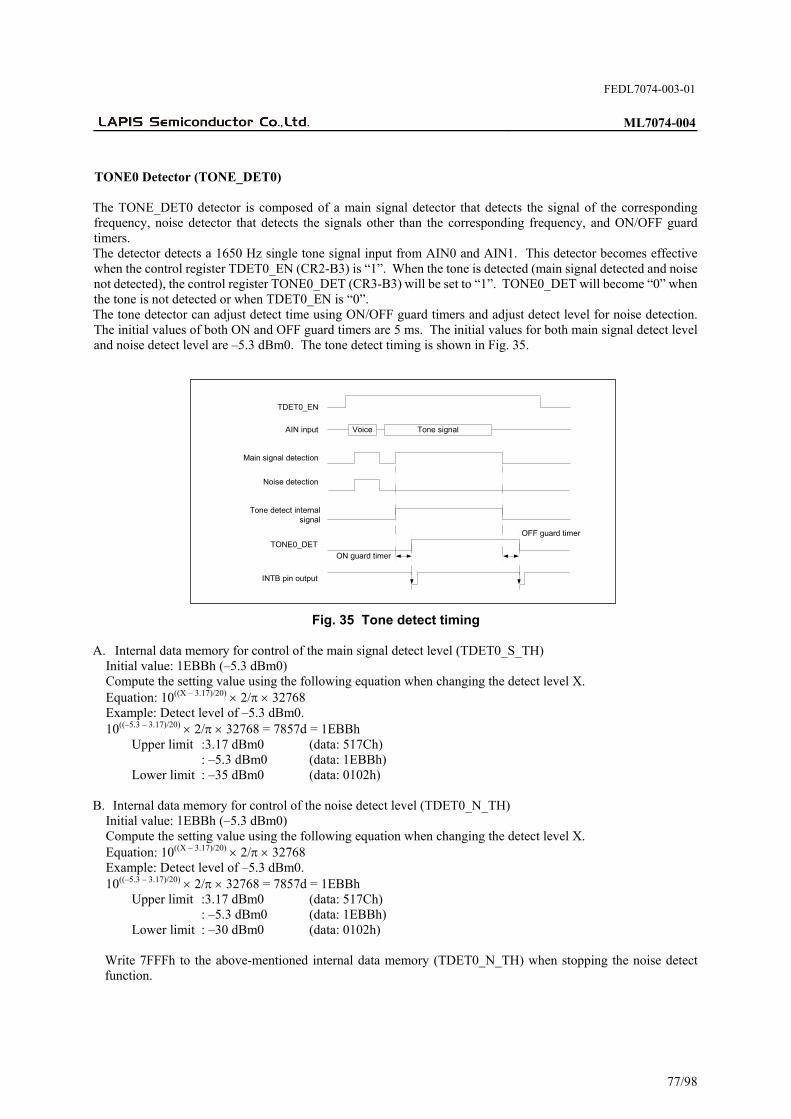
FEDL7074-003-01
ML7074-004
77/98
TONE0 Detector (TONE_DET0) The TONE_DET0 detector is composed of a main signal detector that detects the signal of the corresponding frequency, noise detector that detects the signals other than the corresponding frequency, and ON/OFF guard timers. The detector detects a 1650 Hz single tone signal input from AIN0 and AIN1. This detector becomes effective when the control register TDET0_EN (CR2-B3) is “1”. When the tone is detected (main signal detected and noise not detected), the control register TONE0_DET (CR3-B3) will be set to “1”. TONE0_DET will become “0” when the tone is not detected or when TDET0_EN is “0”. The tone detector can adjust detect time using ON/OFF guard timers and adjust detect level for noise detection. The initial values of both ON and OFF guard timers are 5 ms. The initial values for both main signal detect level and noise detect level are –5.3 dBm0. The tone detect timing is shown in Fig. 35.
Fig. 35 Tone detect timing A. Internal data memory for control of the main signal detect level (TDET0_S_TH)
Initial value: 1EBBh (–5.3 dBm0) Compute the setting value using the following equation when changing the detect level X. Equation: 10((X – 3.17)/20) 2/ 32768 Example: Detect level of –5.3 dBm0. 10((–5.3 – 3.17)/20) 2/ 32768 = 7857d = 1EBBh
Upper limit :3.17 dBm0 (data: 517Ch) : –5.3 dBm0 (data: 1EBBh) Lower limit : –35 dBm0 (data: 0102h)
B. Internal data memory for control of the noise detect level (TDET0_N_TH)
Initial value: 1EBBh (–5.3 dBm0) Compute the setting value using the following equation when changing the detect level X. Equation: 10((X – 3.17)/20) 2/ 32768 Example: Detect level of –5.3 dBm0. 10((–5.3 – 3.17)/20) 2/ 32768 = 7857d = 1EBBh
Upper limit :3.17 dBm0 (data: 517Ch) : –5.3 dBm0 (data: 1EBBh) Lower limit : –30 dBm0 (data: 0102h)
Write 7FFFh to the above-mentioned internal data memory (TDET0_N_TH) when stopping the noise detect function.
TDET0_EN
AIN input Tone signal
Main signal detection
Noise detection
Voice
OFF guard timer
INTB pin output
TONE0_DET
ON guard timer
Tone detect internalsignal
FEDL7074-003-01
ML7074-004
78/98
C. Internal data memory for the detect ON guard timer (TDET0_ON_TM)
Initial value: 0028h (5 ms) Use the following equation when changing the timer value. Equation: Guard timer value in ms/0.125 ms Example: 5 ms 5/0.125 = 40d = 0028h
Upper limit : 4095.875 ms (data: 7FFFh) : 5 ms (data: 0028h) Lower limit : 0.125 ms (data: 0001h)
D. Internal data memory for the detect OFF guard timer (TDET0_OFF_TM)
Initial value: 0028h (5 ms) Use the following equation when changing the timer value. Equation: Guard timer value in ms/0.125 ms Example: 5 ms 5/0.125 = 40d = 0028h
Upper limit : 4095.875 ms (data: 7FFFh) : 5 ms (data: 0028h) Lower limit : 0.125 ms (data: 0001h)
E. Internal data memory for controlling the detect frequency (TDET0_FREQ)
Initial value: — The detect frequency can be changed. Contact ROHM's responsible sales person when you wish to change the detect frequency.

FEDL7074-003-01
ML7074-004
79/98
TONE1 Detector (TONE_DET1) The TONE_DET1 detector is composed of a main signal detector that detects the signal of the corresponding frequency, noise detector that detects the signals other than the corresponding frequency, and ON/OFF guard timers. The detector detects a 2100 Hz single tone signal input from AIN0 and AIN1. This detector becomes effective when the control register TDET1_EN (CR2-B4) is “1”. When the tone is detected (main signal detected and noise not detected), the control register TONE1_DET (CR3-B4) will be set to “1”. TONE1_DET will become “0” when the tone is not detected or when TDET1_EN is “0”. The tone detector can adjust detect time using ON/OFF guard timers and adjust detect level for noise detection. The initial values of both ON and OFF guard timers are 5 ms. The initial values for both main signal detect level and noise detect level are –5.3 dBm0. The tone detect timing is shown in Fig. 36.
Fig. 36 Tone detect timing A. Internal data memory for control of the main signal detect level (TDET1_S_TH)
Initial value: 1EBBh (–5.3 dBm0) Compute the setting value using the following equation when changing the detect level X. Equation: 10((X – 3.17)/20) 2/ 32768 Example: Detect level of -5.3 dBm0. 10((–5.3 – 3.17)/20) 2/ 32768 = 7857d = 1EBBh
Upper limit : 3.17 dBm0 (data: 517Ch) : –5.3 dBm0 (data: 1EBBh) Lower limit : –35 dBm0 (data: 0102h)
B. Internal data memory for control of the noise detect level (TDET0_N_TH)
Initial value: 1EBBh (–5.3 dBm0) Compute the setting value using the following equation when changing the detect level X. Equation: 10((X – 3.17)/20) 2/ 32768 Example: Detect level of –5.3 dBm0. 10((–5.3 – 3.17)/20) 2/ 32768 = 7857d = 1EBBh
Upper limit :3.17 dBm0 (data: 517Ch) : –5.3 dBm0 (data: 1EBBh) Lower limit : –30 dBm0 (data: 0102h)
Write 7FFFh to the above-mentioned internal data memory (TDET1_N_TH) when stopping the noise detect function.
TDET1_EN
AIN input Tone signal
Main signal detection
Noise detection
Voice
OFF guard timer
INTB pin output
TONE1_DET
ON guard timer
Tone detect internalsignal

FEDL7074-003-01
ML7074-004
80/98
C. Internal data memory for the detect ON guard timer (TDET1_ON_TM)
Initial value: 0028h (5 ms) Use the following equation when changing the timer value. Equation: Guard timer value in ms/0.125 ms Example: 5 ms 5/0.125 = 40d = 0028h
Upper limit : 4095.875 ms (data: 7FFFh) : 5 ms (data: 0028h) Lower limit : 0.125 ms (data: 0001h)
D. Internal data memory for the detect OFF guard timer (TDET1_OFF_TM)
Initial value: 0028h (5 ms) Use the following equation when changing the timer value. Equation: Guard timer value in ms/0.125 ms Example: 5 ms 5/0.125 = 40d = 0028h
Upper limit : 4095.875 ms (data: 7FFFh) : 5 ms (data: 0028h) Lower limit : 0.125 ms (data: 0001h)
E. Internal data memory for controlling the detect frequency (TDET1_FREQ)
Initial value: — The detect frequency can be changed. Contact ROHM's responsible sales person when you wish to change the detect frequency.

FEDL7074-003-01
ML7074-004
81/98
DTMF Detector (DTMF_REC) This section detects the DTMF signal input from AIN. The DTMF detector is made up of a DTMF detection block that detects the DTMF signal, a noise detection block that detects signals other than the DTMF signal, an ON guard timer, and an OFF guard timer. The DTMF detector becomes effective when the control register DTMF_EN (CR2-B2) is “1”, and when a valid DTMF signal is detected, DTMF_DET (CR4-B4) becomes “1” and the received code is stored in DTMF_0 to DTMF_3 (CR4-B3, 2, 1, 0). When no DTMF signal is detected or when DTMF_EN is “0”, DTMF_DET will be “0” and also DTMF_0 to DTMF_3 will be “0000”. The DTMF detect timing is shown in Fig. 38. The DTMF detector is composed of a detector section, an ON guard timer, and an OFF guard timer. The detect time and the detect level can be adjusted. The initial values of both ON and OFF guard timers are 20 ms. The initial value of the detect level is –37.0 dBm0.
Fig. 37 DTMF detect timing A. Internal data memory for gain adjustment (DTMF_TH)
Initial value: 1000h (–37.0 dBm0) Compute the setting value using the following equation when changing the detect level. Equation: 1000h 1 / GAIN Example: Increasing the detect level by 6 dB. 1000h 0.5 = 0800h
Upper limit : 12 dB higher (data: 0400h) Lower limit : 12 dB lower (data: 4000h)
Note: The detection level set in the above data memory (DTMF_TH) is the common detection level of the DTMF detection block and the noise detection block.
B. Internal data memory for the ON guard timer (DTMF_ON_TM)
Initial value: 00A0h (20 ms) Use the following equation when changing the timer value. Equation: Guard timer value in ms/0.125 ms Example: 5 ms 5/0.125 = 40d = 0028h
Upper limit : 4095.875 ms (data: 7FFFh) : 5 ms (data: 0028h) Lower limit : 0.125 ms (data: 0001h)
DTMF_EN
AIN input DTMF signalVoice
DTMF_DET
DTMFcode output(DTMF_CODE[3:0])
"0000" Detected code "0000"
ON guard timer OFF guard timer
INTB pin output
DTMF detect section
Noise detect section
DTMF detect internalsignal

FEDL7074-003-01
ML7074-004
82/98
C. Internal data memory for the OFF guard timer (DTMF_OFF_TM) Initial value: 00A0h (20 ms) Use the following equation when changing the timer value. Equation: Guard timer value in ms/0.125 ms Example: 5 ms 5/0.125 = 40d = 0028h
Upper limit : 4095.875 ms (data: 7FFFh) : 5 ms (data: 0028h) Lower limit : 0.125 ms (data: 0001h)
D. Internal data memory for noise detection function control (DTMF_NDET_CONT)
Initial value: 0002h (noise detection function enabled) By writing 0000h into this internal data memory, the noise detection function of the DTMF detector is disabled.
Notice: During DTMF signal detection, if the DTMF signal changes to another code successively, the received code changes and an interrupt can be generated with DTMF_DET in the “1” state.
Note: To use this internal data memory by inputting signals in G.711 coding format from the PCM interface, set the input level of the DTMF signal (per wave) at –10 dBmO or lower. If the DTMF signal is input at a level greater than–10 dBmO, the DTMF signal may not be detected normally.

FEDL7074-003-01
ML7074-004
83/98
Echo Canceller The block diagram of the echo canceller is shown in Fig. 38. The echo canceller has a delay time of 32 ms and is activated by setting a “1” in EC_EN (CR2-B1). The operation setting of the echo canceller is done mainly using the internal data memory locations EC_CR and GLPAD_CR.
Fig. 38 Echo canceller block diagram A. Echo canceller control (EC_CR)
Iinitial value: 0012h Write “0” in the higher order 8 bits (B15 to B8)
B7 B6 B5 B4 B3 B2 B1 B0
THR HLD HDB CLP ATTB
Initial value 0 0 0 1 0 0 1 0
B7: Through mode control 1: Through mode 0: Normal mode (echo cancel operation) When this through mode control bit of the echo canceller is set, the data of Rin and Sin are output directly to Rout and Sout while retaining their respective echo coefficients. Further, during the through mode, the HLD, HDB, ATTB and CLP functions are disabled.
B6: Reserved bit. Prohibited to change the initial value. B5: Coefficient update control 1: Coefficient fixed 0: Coefficient updated This bit selects the presence or absence of updating of the adaptive FIR filter (AFF) coefficient of the echo canceller. This function becomes valid when THR is in the normal mode.
Echo Canceller
+
-
AdaptiveFIR Filter(AFF)
LPAD GPAD
ATTs
ATTr
CenterClip
Sin
Rout
Sout
Rin
Power Calc
Howling Detector
Double Talk Det

FEDL7074-003-01
ML7074-004
84/98
B4: Howling detector control 1: OFF 0: ON This bit controls the function of detecting and removing howling which is generated in a hands-free acoustic system, etc. This function becomes valid when THR is in the normal mode.
B3: Center clip control 1: ON 0: OFF This bit controls the center clip function in which the Sout output is forcibly fixed to the minimum positive value when the Sout output of the echo canceller is –57 dBm0 or less. This function becomes valid when THR is in the normal mode.
B2: Reserved bit. Prohibited to change the initial value.
B1: Attenuator control 1: ATT OFF 0: ATT ON This bit selects the switching ON/OFF of the ATT function which prevents howling using the attenuators ATTs and ATTr provided at the Rin input and Sout output of the echo canceller. When only the Rin input is present, the attenuator (ATTs) of Sout will be inserted. When only the Sin input is present or when both the Sin and Rin inputs are present, the attenuator (ATTr) of Rin will be inserted. The respective attenuation values are 6 dB. This function becomes valid when THR is in the normal mode. B0: Reserved bit. Prohibited to change the initial value.
B. GLPAD control (GLPAD_CR)
Initial value: 000Fh This data memory controls the GLPAD within the echo canceller. Write “0” in the higher order 8 bits (B15 to B8).
B7 B6 B5 B4 B3 B2 B1 B0
GPAD2 GPAD1 LPAD2 LPAD1
Initial value 0 0 0 0 1 1 1 1
B7, 6, 5, 4: Reserved bits. B3, 2: Output level control These bits control the GPAD level for the echo canceller output gain. (0, 1): +18 dB (0, 0): +12 dB (1, 1): +6 dB (1, 0): 0 dB B1, 0: Input level control These bits control the LPAD level for the echo canceller input loss. (0, 1): –18 dB (0, 0): –12 dB (1, 1): –6 dB (1, 0): 0 dB

FEDL7074-003-01
ML7074-004
85/98
C. Precautions in using the Echo Canceller
C-1 In the echo path, make sure that the echo signal does not cause saturation, waveform distortion, etc., in the external amplifier, etc. The echo attenuation becomes poor if any saturation or waveform distortion occur. C-2 Make the settings so that the echo return loss (E.R.L.) is attenuating. Further, it is recommended to use the GLPAD function if the E.R.L. is set to be amplified. The echo attenuation gets deteriorated seriously if the E.R.L. is set to be amplified. The E.R.L. is the attenuation (loss) of echo amount from the echo canceller output (Rout) to the echo canceller input (Sin). C-3 When the echo path can change (such as during a reconnected call), it is recommended to carry out a reset using EC_EN (CR2-B1), PDNB, or SPDN (CR0-B7).

FEDL7074-003-01
ML7074-004
86/98
Dial Pulse Detector (DPDET) Dial pulse signals input at the general-purpose input pin GPI0 are detected by this DPDET. The dial pulse detector becomes effective when the control register bit DPDET_EN (CR10-B6) is “1”. DP_DET (CR4-B6) becomes “1” when a dial pulse signal is detected and the detected number of dial pulses is stored in DPDET_CODE. The number of dial pulses detected should be read out from DPDET_CODE at the time when DP_DET goes from “1” to “0”. When a dial pulse signal is not detected, or when DPDET_EN is “0”, DP_DET will remain “0”. The dial pulse detect timing is shown in Fig. 39. The dial pulse detector samples the dial pulse signal input at GPI0 at 8 kHz sampling rate, and detects the dial pulses based on the settings of the ON guard timer (DPDET_ON_TIM) and OFF guard timer (DPDET_OFF_TIM). Further, it is possible to adjust the detect end time by setting the detect end timer (DPDET_DETOFF_TIM).
Fig. 39 Dial pulse detect timing A. Dial pulse detect control register (DPDET_EN CR10-B6)
0: Dial pulse detection stopped 1: Dial pulse detection active
B. Dial pulse detector detect status register (DP_DET CR4-B6)
0: Dial pulses not detected 1: Dial pulses detected This bit is set to “1” after DPDET_EN has been set when an edge at GPI0 is detected. Further, if no edge is detected for a period set in DPDET_DETOFF_TIM after an edge detection, this bit will be cleared automatically to “0”.
GPI0
Status of Internaldetection
DPDET_OFF_TIM
DPDET_ON_TIM
Status of internal detection by guard timer
DP detect timing
DPDET_EN
GPI0
(Internal signal after masked by guard timer)
DP_DET
DPDET_DETOFF_TIMDPDET_DETOFF_TIM
DPDET_CODE 1 2 30 1 0
INTB

FEDL7074-003-01
ML7074-004
87/98
C. Internal data memory for ON guard timer (DPDET_ON_TIM) Iinitial value: 0028h (5 ms) Use the following equation when changing the timer value. Equation: Guard timer value in ms/0.125 ms Example: 5 ms 5/0.125 = 40d = 0028h
Upper limit : 4095.875 ms (data: 7FFFh) : 5 ms (data: 0028h) Lower limit : 0.125 ms (data: 0001h)
D. Internal data memory for OFF guard timer (DPDET_OFF_TIM)
Initial value: 0028h (5 ms) Use the following equation when changing the timer value. Equation: Guard timer value in ms/0.125 ms Example: 5 ms 5/0.125 = 40d = 0028h
Upper limit : 4095.875 ms (data: 7FFFh) : 5 ms (data: 0028h) Lower limit : 0.125 ms (data: 0001h)
E. Internal data memory for detect polarity control (DPDET_POL)
Iinitial value: 0000h (no polarity reversal) Controls the polarity of the input from GPI0.
0000h: No polarity reversal 0001h: Polarity reversal present
F. Internal data memory for detect end control (DPDET_DETOFF_TIM)
Initial value: 03E8h (125 ms) Use the following equation when changing the timer value. Equation: Guard timer value in ms/0.125 ms Example: 125 ms 125/0.125 = 1000d = 03E8h
Upper limit : 4095.875 ms (data: 7FFFh) : 125 ms (data: 03E8h) Lower limit : 0.125 ms (data: 0001h)
G. Internal data memory for indicating number of detected pulses (DPDET_CODE) Initial value: 0000h (not-detected state) Indicates the number of detected pulses. This internal data memory for indication is updated when an edge is detected.
Notice: Ignore the interrupt occurred after the time set by the ON guard timer if the DPDET is activated under the following conditions:
DPDET_POL = “0”, GPI0 = “1” DPDET_POL = “1”, GPI0 = “0”

FEDL7074-003-01
ML7074-004
88/98
Dial Pulse Transmitter (DPGEN) The dial pulse transmitter outputs a dial pulse signal at the general-purpose output pin GPO0. The dial pulse generation will be effective when the control memory bit DPGEN_EN is “1”, and a dial pulse signal is output with the number of pulses set in DPGEN_DATA. The dial pulse output timing is shown in Fig. 40. The speed (rate) of dial pulses can be selected to be 10PPS or 20PPS by setting DPGEN_PPS accordingly. Further, it is possible to adjust the make/break ratio by setting the break duration using DPGEN_DUTY. Also, the output polarity of the dial pulse signal can be changed by DPGEN_POL.
The maks/break ratio can be adzusted by setting the break duration(DPGEN_DUTY)
- 10PPS/output polarity : Posive logic/ 10 output pulses
GPO0
DPGEN_OFF_TIM
DPGEN_EN
- 10PPS/Output palarity : Negative logic/ 2 output pulses
DPGEN_OFF_TIM
0.1sec/10PPS (0.05sec/20PPS)
GPO0
DPGEN_EN
- Output polarity setting, maks/break ratio adzustment
The output polarity can be changed (DPGEN_POL).
Positive logic
Negative logic
Breakduration
Breakduration
Breakduration
Breakduration
GPO0
GPO0
Fig. 40 Dial pulse output timing
A. Internal data memory for dial pulse transmit control (DPGEN_EN)
Initial value: 0000h The dial pulses are transmitted when a “0001h” is written in this data memory. This data memory will be cleared automatically after a period of time set in DPGEN_OFF_TIM.
0000h: Dial pulse output stopped 0001h: Dial pulse output active
Notice: Activate DPGEN with CR17-B0 (GPO0) being in the “0” state, according to the setting of internal of data memory for output polarity control (DPGEN_POL).
DPGEN_POL =0000h (positive logic) : CR17-B0 (GPO0) = “0” DPGEN_POL =0001h (negative logic) : CR17-B0 (GPO0) = “1”

FEDL7074-003-01
ML7074-004
89/98
B. Internal data memory for setting the number of pulses (DPGEN_DATA)
Initial value: 0000h Upper limit: 10 (data: 000Ah) Lower limit: 1 (data: 0001h)
C. Internal data memory for dial pulse rate control (DPGEN_PPS)
Initial value: 0000h 0000h: 10 PPS 0001h: 20 PPS
D. Internal data memory for controlling make/break ratio (DPGEN_DUTY)
Initial value: 0108h (33 ms/10 PPS, 16.5 ms/20 PPS) Use the following equation when setting the “break” duration. The value will be half this set value in the case of 20 PPS. Equation: “break” output time duration in ms/0.125 ms Example: 33 ms 33/0.125 = 264d = 0108h
Upper limit : 100 ms (data: 0320h) : 33 ms (data: 0108h) Lower limit : 0.125 ms (data: 0001h)
E. Internal data memory for end of output control (DPGEN_OFF_TIM)
Initial value: 03E8h (125 ms) Use the following equation when setting the end of output control. Equation: End of output time duration in ms/0.125 ms Example: 125 ms 125/0.125 = 1000d = 03E8h
Upper limit : 4095.875 ms (data: 7FFFh) : 125 ms (data: 03E8h) Lower limit : 0 ms (data: 0000h)
F. Internal data memory for output polarity control (DPGEN_POL)
Initial value: 0000h Controls the polarity of output from GPO0.
Setup value: 0000h Positive logic (Low: make segment, High: break segment) Setup value: 0001h Negative logic (Low: break segment, High: make segment)

FEDL7074-003-01
ML7074-004
90/98
Timer (TIMER) This is a 16-bit up-counter timer. When a “0001h” is set in the internal memory for timer control (TIM_EN), the timer starts counting up the timer count (TIM_COUNT) at every 125 s. When the timer count value becomes equal to the timer data value, the timer counter value will be reset to “0000h” and the timer starts counting up again. A. Internal data memory for timer control (TIM_EN)
Iinitial value: 0000h The timer starts counting up when “0001h” is written in this data memory location. When a “0000h” is set here, the counting up will be stopped and the counter value will be cleared.
0000h: Stops counting 0001h: Starts counting
B. Internal data memory for timer count indication (TIM_COUNT)
Initial value: 0000h C. Internal data memory for timer data (TIM_DATA)
Initial value: FFFFh Upper limit : 8192 ms (data: FFFFh) Lower limit : 0.250 ms (data: 0001h)

FEDL7074-003-01
ML7074-004
91/98
Outband Control (OUTBAND_CONTROL) This is a function is automatically to mute or to write silence data in Tx buffer when corresponding detection bit (***_DET) gets “1”. Either to mute or to write silence data in Tx buffer differs among speech codec’s as shown below;
G.711 (-/A-law) Mutes speech data given to codec G.729.A Writes silence data (80 bits) in Tx buffer The 80 bits meaning silence in G.729.A to write in Tx buffer as default could be
altered any 80 bits you like in the initial mode. Initial value : 0000h
B7 B6 B5 B4 B3 B2 B1 B0
TDET1
_OB_EN
TDET0
_OB_EN
DTMFDET
_OB_EN
Initial Value 0 0 0 0 0 0 0 0
B7, 6, 5, 4, 3 : Reserved bits B2 : TDET1_OUTBAND_EN control 1 : ON (Mutes speech data given to codec when TDET1_DET is “1”) 0 : OFF B1 : TDET0_OUTBAND_EN control 1 : ON (Mutes speech data given to codec when TDET0_DET is “1”) 0 : OFF B0 : DTMFDET_OUTBAND_EN control 1 : ON (Writes data specified by OUTBAND_G729_DAT which is silence as default when
DTMF_DET is “1”) 0 : OFF
- Leak time of tones to Tx buffer
A referential equation for leak time of tones to Tx buffer with each speech codec is shown below;
G.711 0ms + A + B G.729.A -10ms to -20ms + A + B
* -10ms to -20ms by prediction and framing process
A : detection delay time of a given detector (ms) Depends upon input level, frequency, etc.. B : ON-guard timer time of a given detector
< Example> If the detect delay time of a detector is about 30 ms and the ON-guard timer time of a detector is 20 ms, the leak time to the Tx buffer is shown below. G.711 30ms (A) + 20m s (B) = approx. 50ms G.729.A (-10ms to -20ms) + 20ms (A) + 20ms (B) = approx. 30ms to 40ms
Outband G.729.A data (OUTBAND_G729_DAT) When outband control is made in G.729.A mode, the data in the addresses below are written into Tx buffer when corresponding detection bit (***_DET) gets “1”. The data to write into Tx buffer could be altered in the initial mode.
Address: 00A6h 00A7h 00A8h 00A9h 00AAh Initial value: 7852h 80A0h 00FAh C200h 07D6h

FEDL7074-003-01
ML7074-004
92/98
LSI Code Indication (ML7074_VERSION) The code ML7074-004 is indicated here. Value: 0003h

FEDL7074-003-01
ML7074-004
93/98
EXAMPLE OF CONFIGURATION Analog I/F mode
Echo Canceller
DTMF_REC
+
-
AFF
D/A LPF
G.729.A
TONE_GEN0(TONEA/B)
TX Buffer0
RX Buffer0
Frame/DMAController
INTB
A0-A7
ControlRegister
8b
D0-D1516b
VREF CSB
RDB
WRB
FR0B
FR1B
ACK0B
ACK1B
AIN1N
GSX1
VFRO0
AVREF
OSC Power
PLL
Speech Codec
10k
10k
DV
DD
2
DG
ND
2
AV
DD
AG
ND
PD
NB
TS
T1XI
XO
G.711
TXGAIN
RXGAIN
DV
DD
1
DG
ND
1
DV
DD
0
DG
ND
0
TS
T2
TS
T3
CKGNMCKSYNC(8kHz)
LPAD GPAD
ATTs
ATTr
Bus Control Unit
CenterClip
Encoder
G.729.A
G.711
Decoder
DTMF_DET
INT
DTMF_DET
TX Buffer1
RX Buffer1
AIN0N
GSX0
10k
AIN0P
Linear PCM Codec
VFRO110k
STGAIN
SYNC
BCLK
PCMI
PCMO
TONE_DET1 TONE1_DET
S/P
P/S
Serial I/F
TONE0_DETTONE1_DET
GP
I0
GP
I1
GP
O0
GP
O1
TONE_DET0 TONE0_DET
FSK_GEN
TS
T0
CLKSEL
AMP0
AMP1
AMP2
AMP3
Sin
Rout
Sout
Rin
A/D BPF
Codec
DPGEN
DPDETCR16-B0(GPI0)
CR17-B0(GPO0)
DP_DET
DP_DET
TIMER
DTMF_CODE[3:0]
DTMF_CODE[3:0]
TONE_GEN1(TONEC/D)
G.711
Encoder
G.711
Decoder
FGEN_FLAG
FGEN_FLAG
Function stoppedCannot be used
Example of settings in the initialization mode CR15 = 40h * This is mandatory. CR6=0Fh,CR7=FFh,CR8=00h,CR9=01h,CR1=80h (Address : 0FFFh, Data : 0001h) * This is mandatory. As for how to set them, refer to Method of Accessing and Controlling Internal Data Memory. CR11 = 00h (Frame/10 ms/16B/Speech CODEC = G.729.A) Various settings CR0 = 09h (OPE_STAT = “1”)
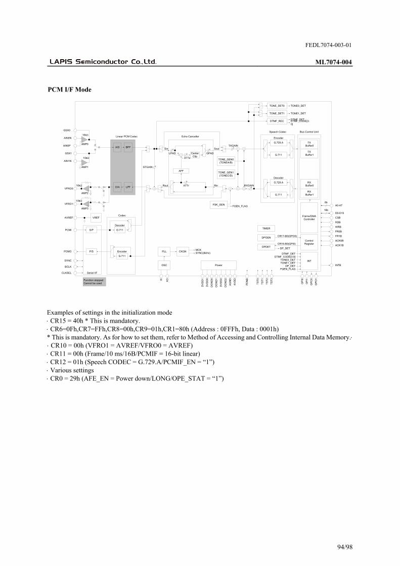
FEDL7074-003-01
ML7074-004
94/98
PCM I/F Mode
Echo Canceller
DTMF_REC
+
-
AFF
D/A LPF
G.729.A
TONE_GEN0(TONEA/B)
TX Buffer0
RX Buffer0
Frame/DMAController
INTB
A0-A7
ControlRegister
8b
D0-D1516b
VREF CSB
RDB
WRB
FR0B
FR1B
ACK0B
ACK1B
AIN1N
GSX1
VFRO0
AVREF
OSC Power
PLL
Speech Codec
10k
10k
DV
DD
2
DG
ND
2
AV
DD
AG
ND
PD
NB
TS
T1XI
XO
G.711
TXGAIN
RXGAIN
DV
DD
1
DG
ND
1
DV
DD
0
DG
ND
0
TS
T2
TS
T3
CKGNMCKSYNC(8kHz)
LPAD GPAD
ATTs
ATTr
Bus Control Unit
CenterClip
Encoder
G.729.A
G.711
Decoder
DTMF_DET
INT
DTMF_DET
TX Buffer1
RX Buffer1
AIN0N
GSX0
10k
AIN0P
Linear PCM Codec
VFRO110k
STGAIN
SYNC
BCLK
PCMI
PCMO
TONE_DET1 TONE1_DET
S/P
P/S
Serial I/F
TONE0_DETTONE1_DET
GP
I0
GP
I1
GP
O0
GP
O1
TONE_DET0 TONE0_DET
FSK_GEN
TS
T0
CLKSEL
AMP0
AMP1
AMP2
AMP3
Sin
Rout
Sout
Rin
A/D BPF
Codec
DPGEN
DPDETCR16-B0(GPI0)
CR17-B0(GPO0)
DP_DET
DP_DET
TIMER
DTMF_CODE[3:0]
DTMF_CODE[3:0]
TONE_GEN1(TONEC/D)
G.711
Encoder
G.711
Decoder
Function stoppedCannot be used
FGEN_FLAG
FGEN_FLAG
Examples of settings in the initialization mode CR15 = 40h * This is mandatory. CR6=0Fh,CR7=FFh,CR8=00h,CR9=01h,CR1=80h (Address : 0FFFh, Data : 0001h) * This is mandatory. As for how to set them, refer to Method of Accessing and Controlling Internal Data Memory. CR10 = 00h (VFRO1 = AVREF/VFRO0 = AVREF) CR11 = 00h (Frame/10 ms/16B/PCMIF = 16-bit linear) CR12 = 01h (Speech CODEC = G.729.A/PCMIF_EN = “1”) Various settings CR0 = 29h (AFE_EN = Power down/LONG/OPE_STAT = “1”)

FEDL7074-003-01
ML7074-004
95/98
EXAMPLE OF APPLICATION CIRCUIT
49
AVREF
VFRO0
VFRO1
AVDD
50
51
52
53
54
55
56
57
58
59
60
61
62
63
3231
30
29
28
27
26
25
24
23
22
21
20
19
18
17
TST3
TST2
DGND2
XI
XO
DVDD2
AIN1N
GSX1
AIN0P
AIN0N
GSX0
AGND
ML7074
1
2
3
4
5
6
7
8
9
10
11
12
1314
15
DGND0
TST1
TST0
PCMO
PCMI
BCLK
SYNC
RDB
WRB
CSB
FR0B
FR1B
DVDD0
INTB
ACK0B
ACK1B
48
47
46
45
44
43
42
41
40
39
38
37
36
35
34
33
DGND1
DVDD1
A0
A1
A2
A3
A4
A5
A6
A7
GPI0
GPI1
GPO0
GPO1
PDNB
CLKSEL
D15
D14
D13
D12
D11
D10
D9
D8
D7
D6
D5
D4
D3
D2
D1
D0
64
+3.3V
+3.3V
+3.3V
open
open
open
Power down control
MCUI/F
General-purpose
input pins
4.096 MHzcrystal
oscillator
Analoginput
PCMI/F
Analogoutput
Conditions:- When using analog interface- Frame mode- SYNC and BCLK are output (CLKSEL="1")
General-purpose
output pins
16
1.4V

FEDL7074-003-01
ML7074-004
96/98
PACKAGE DIMENSIONS
QFP64-P-1414-0.80-BK
Mirror finish
Package material Epoxy resinLead frame material 42 alloyPin treatment Solder plating (�5μm)Package weight (g) 0.87 TYP.5Rev. No./Last Revised 6/Feb. 23, 2001
Notes for Mounting the Surface Mount Type Package The surface mount type packages are very susceptible to heat in reflow mounting and humidity absorbed in storage. Therefore, before you perform reflow mounting, contact ROHM's responsible sales person for the product name, package name, pin number, package code and desired mounting conditions (reflow method, temperature and times).
(Unit: mm)

FEDL7074-003-01
ML7074-004
97/98
REVISION HISTORY
Page Document
No. Date Previous
EditionCurrentEdition
Description
FEDL7074-004-01 Nov. 12, 2003 – – Final edition 1

FEDL7074-003-01
ML7074-004
98/98
NOTICE
No copying or reproduction of this document, in part or in whole, is permitted without the consent of LAPIS Semiconductor Co., Ltd.
The content specified herein is subject to change for improvement without notice.
The content specified herein is for the purpose of introducing LAPIS Semiconductor's products (hereinafter "Products"). If you wish to use any such Product, please be sure to refer to the specifications, which can be obtained from LAPIS Semiconductor upon request.
Examples of application circuits, circuit constants and any other information contained herein illustrate the standard usage and operations of the Products. The peripheral conditions must be taken into account when designing circuits for mass production.
Great care was taken in ensuring the accuracy of the information specified in this document. However, should you incur any damage arising from any inaccuracy or misprint of such information, LAPIS Semiconductor shall bear no responsibility for such damage.
The technical information specified herein is intended only to show the typical functions of and examples of application circuits for the Products. LAPIS Semiconductor does not grant you, explicitly or implicitly, any license to use or exercise intellectual property or other rights held by LAPIS Semiconductor and other parties. LAPIS Semiconductor shall bear no responsibility whatsoever for any dispute arising from the use of such technical information.
The Products specified in this document are intended to be used with general-use electronic equipment or devices (such as audio visual equipment, office-automation equipment, communication devices, electronic appliances and amusement devices).
The Products specified in this document are not designed to be radiation tolerant.
While LAPIS Semiconductor always makes efforts to enhance the quality and reliability of its Products, a Product may fail or malfunction for a variety of reasons.
Please be sure to implement in your equipment using the Products safety measures to guard against the possibility of physical injury, fire or any other damage caused in the event of the failure of any Product, such as derating, redundancy, fire control and fail-safe designs. LAPIS Semiconductor shall bear no responsibility whatsoever for your use of any Product outside of the prescribed scope or not in accordance with the instruction manual.
The Products are not designed or manufactured to be used with any equipment, device or system which requires an extremely high level of reliability the failure or malfunction of which may result in a direct threat to human life or create a risk of human injury (such as a medical instrument, transportation equipment, aerospace machinery, nuclear-reactor controller, fuel-controller or other safety device). LAPIS Semiconductor shall bear no responsibility in any way for use of any of the Products for the above special purposes. If a Product is intended to be used for any such special purpose, please contact a ROHM sales representative before purchasing.
If you intend to export or ship overseas any Product or technology specified herein that may be controlled under the Foreign Exchange and the Foreign Trade Law, you will be required to obtain a license or permit under the Law.
Copyright 2011 LAPIS Semiconductor Co., Ltd.