ferroelectric polarization in ch nh pbi perovskitenesel.skku.edu/paper files/147.pdf · ·...
TRANSCRIPT

Ferroelectric Polarization in CH3NH3PbI3 PerovskiteHui-Seon Kim,†,⊥ Sung Kyun Kim,‡,⊥ Byeong Jo Kim,‡,⊥ Kyung-Sik Shin,‡ Manoj Kumar Gupta,‡
Hyun Suk Jung,‡ Sang-Woo Kim,*,‡,§ and Nam-Gyu Park*,†
†School of Chemical Engineering and Department of Energy Science, ‡School of Advanced Materials Science and Engineering, and§SKKU Advanced Institute of Nanotechnology, Sungkyunkwan University, Suwon 440-746, Korea
ABSTRACT: We report on ferroelectric polarization behaviorin CH3NH3PbI3 perovskite in the dark and under illumination.Perovskite crystals with three different sizes of 700, 400, and100 nm were prepared for piezoresponse force microscopy(PFM) measurements. PFM results confirmed the formationof spontaneous polarization in CH3NH3PbI3 in the absence ofelectric field, where the size dependency to polarization wasnot significant. Whereas the photoinduced stimulation was notsignificant without an external electric field, the stimulatedpolarization by poling was further enhanced under illumina-tion. The retention of ferroelectric polarization was alsoobserved after removal of the electric field, in which larger crystals showed longer retention behavior compared to the smallersized one. Additionally, we suggest the effect of perovskite crystal size (morphology) on charge collection at the interface of theferroelectric material even though insignificant size dependency in electric polarization was observed.
Since the reports on perovskite solar cells based on themesoscopic sensitization concept1 and the mesosuperstruc-
tured extremely thin layer concept2 in 2012, organometal halideperovskite has been considered as a promising light harvesterfor high-efficiency solar cells. The power conversion efficiency(PCE) of perovskite solar cells surged to over 15% in 2013 bymodifying a perovskite deposition method from a conventionalone-step method to two-step sequential deposition3 and vaporevaporation process.4 So far, the highest PEC of 19.3% wasreported using a planar structure,5 and 20.1% was certified bythe National Renewable Energy Laboratory.6 The outstandingphotovoltaic performance from perovskite solar cells has urgedresearchers to investigate the fundamental properties ofperovskite. Consequently, balanced charge transport7,8 andcharge accumulation9 properties of organolead iodide perov-skite were unraveled.Besides light harvesting and balanced charge transport
properties, unusual properties were observed withCH3NH3PbI3 (MAPbI3), such as the ambipolar self-dopingproperty,10 high dielectric constant,11 current−voltage hyste-resis,12 and slow dynamics.13 Polarization was suggested as oneof the bases for the origin of these phenomena. In ABO3 oxideperovskite materials, ferroelectricity along with high dielectricconstants was observed.14 In addition, a phase transition wasaccompanied in ferroelectric oxide perovskite materials. Thus,anomalous properties observed for MAPbI3 are likely to berelated to the underlying ferroelectric property because of itshigh dielectric constant and cubic−tetragonal phase transition.Regarding the issue on ferroelectricity in MAPbI3, theoreticalcalculations suggested the possibility of ferroelectricity ofMAPbI3.
15−17 Ferroelectric domains were directly observedfrom the solution-processed MAPbI3.
18 Interestingly, no
ferroelectricity was measured from MAPbI3, but the ionmigration was suggested to interpret the phenomena.10,19
This means that the argument on ferroelectricity in MAPbI3 hasnot been terminated with clear conclusion, which motivates usto investigate the ferroelectric behavior of MAPbI3.We report here on ferroelectric polarization behavior in
MAPbI3 by a piezoresponse force microscopy (PFM)investigation. We measured the electric polarization change ofthe samples with different crystal size with and without anelectric field in the dark and under illumination. In addition,polarization retention characteristics after removal of theexternal electric field were investigated. All experiments weredesigned similar to the practical solar cell operation includingthe morphology of MAPbI3 and the range of the externalelectric field in order to closely correlate with the solar cellcharacteristics and give insight into the working principle ofperovskite solar cells.Photovoltaic performance was previously found to be
significantly altered by the crystal size of MAPbI3,20 where a
large crystal was beneficial to light harvesting and chargeextraction compared to a small one. Moreover, a large crystalwas less sensitive to current−voltage (I−V) hysteresis than thesmall one.12 Thus, perovskite layers with different crystal sizeswere selected as samples for PFM study in this work in order tocorrelate the PFM results with the studied photovoltaicproperties. The crystal size was controlled by varying theconcentration of the CH3NH3I (MAI) solution in the two-stepspin-coating deposition method, as described elsewhere,20
Received: April 3, 2015Accepted: April 21, 2015Published: April 21, 2015
Letter
pubs.acs.org/JPCL
© 2015 American Chemical Society 1729 DOI: 10.1021/acs.jpclett.5b00695J. Phys. Chem. Lett. 2015, 6, 1729−1735

where 0.038, 0.044, and 0.063 M MAI produce average MAPbI3crystal sizes of about 700, 400, and 100 nm, respectively, asshown in Figure 1a−c. Compared to the compact nature of the100 nm sized cuboids, the number of gaps appears andincreases upon increasing size, which is consistent with theprevious results.20 No structural change was observed depend-ing on the crystal size, as confirmed by X-ray diffraction (XRD)patterns in Figure 1d−f, which shows that the chemicalcomposition is not modified by crystal size. Because there is nosignificant difference in XRD peaks among three samples withdifferent morphologies, we expect that the grain sizes in thesamples with polycrystalline nature are comparable irrespectiveof the different crystal size. In addition, the prepared MAPbI3shows phase purity without unreacted PbI2.The piezoresponse measurements were conducted using a
PFM setup, as illustrated in Figure 2. The detailed measure-ment condition is described in the Methods section. Toconfirm the ferroelectric characteristics of the MAPbI3, wemeasured the topography and the piezoresponse of the MAPbI3on the fluorine-doped tin oxide (FTO)/glass substrate using
atomic force microscopy (AFM) and PFM. It is well-knownthat PFM is a powerful tool that detects polarization statesbased on the detection of the local piezoelectric deformationinduced by an external electric field in a ferroelectric sample.The topography image of the MAPbI3 was built by measuringthe z-axis movement of the AFM tip in a contact mode. Forpoling the sample, we applied a DC bias voltage between theMAPbI3 cuboid and the conductive tip. During the PFMmeasurement, an AC voltage was applied from the conductivetip as the top electrode to the sample’s surface. The amplitudeand the phase signals of the response of the MAPbI3 material tothe applied electrical signal were detected using the verticaldisplacement of the AFM tip.To determine the ferroelectric polarization of the MAPbI3
perovskite material, positive and negative poling processes weresequentially applied, and the PFM phase was measured both inthe dark and under illumination. Figure 3 shows the PFM phasealong with the topography observed in the dark, where nosignificant deformation of the perovskite sample is assumedthroughout the successive poling process due to the sequentialdistinctive image of the PFM phase. The topographic image ofthe 700 nm sized perovskite sample and the correspondingPFM phase images obtained without bias voltage (unpoled)and with bias voltages of +3 V (positively poled) and −3 V(negatively poled) are depicted in Figure 3a−d, respectively.Figure 3a shows some extent of the PFM phase contrast even inthe absence of an electric field (unpoled), indicative ofspontaneous polarization. Unlike the change in displacementof the B-site cation in oxide perovskites,21,22 the polarizationbehavior in organolead iodide perovskite is likely due to largefreedom of rotation of the polar CH3NH3
+ cation.15 Whenpositive poling (+3 V) is applied, stimulated polarization in thepositive direction is distinctively observed, as shown in Figure3c. Figure 3d shows the PFM image under the negative polingprocess. Interestingly the opposite electric field (−3 V) isincapable of rotating dipoles 180°, which implies that thedipoles cannot easily rotate by the applied electric field due tothe interaction with defects in crystals.23 The spontaneous andstimulated polarizations are also observed for the 400 nm andthe 100 nm sized cuboids. As can be seen in Figure 3f−h andj−l, PFM phase contrast is enhanced upon positive poling andrelieved with negative poling, but the dependence of polar-
Figure 1. Scanning electron microscopy (SEM) images for the MAPbI3 crystals with average cuboid sizes of (a) 700, (b) 400, and (c) 100 nmprepared using 0.038, 0.044, and 0.063 M MAI, respectively. Scale bars represent 500 nm. XRD patterns of (d) 700, (e) 400, and (f) 100 nm sizedMAPbI3 cuboids directly formed on a fluorine-doped tin oxide (FTO) substrate.
Figure 2. Schematic illustration of the experimental setup for PFMstudy of the MAPbI3.
The Journal of Physical Chemistry Letters Letter
DOI: 10.1021/acs.jpclett.5b00695J. Phys. Chem. Lett. 2015, 6, 1729−1735
1730

ization on the crystal size seems to be not significant. It issuggested that the negligible size dependency originates from
the polycrystalline nature of MAPbI3 composed of multiplegrains. Thus, we conclude that grain size is a critical factor to
Figure 3. AFM topographic images and PFM phase images measured in the dark for the MAPbI3 cuboids with size of (a−d) 700, (e−h) 400, and(i−l) 100 nm. Scale bars in (a−h) represent 1 μm, and those in (i−l) represent 500 nm. Measured areas were 5 μm × 5 μm for 700 and 400 nmsized samples and 2 μm × 2 μm for the 100 nm sized sample.
Figure 4. AFM topographic images and PFM phase images measured under illumination (50k lux) for the MAPbI3 cuboids with a size of (a−d) 700,(e−h) 400, and (i−l) 100 nm. Scale bars in (a−h) represent 1 μm, and those in (i−l) represent 500 nm. Measured areas were 5 μm × 5 μm for 700and 400 nm sized samples and 2 μm × 2 μm for the 100 nm sized sample.
The Journal of Physical Chemistry Letters Letter
DOI: 10.1021/acs.jpclett.5b00695J. Phys. Chem. Lett. 2015, 6, 1729−1735
1731

realize effective manipulation of ferroelectric polarization ratherthan crystal morphology. However, careful interpretation is stillneeded considering the fact that the perovskite crystals withdifferent sizes of 700, 400, and 100 nm simultaneously generatedifferent thicknesses of 360, 290, and 170 nm, respectively.Because few studies of the MAPbI3 ferroelectric behavior onthickness effect have been conducted, little information wasgiven to explain the impact of thickness around hundreds ofnanometers.Light-induced polarization of the perovskite cuboids was also
investigated with respect to the crystal size and poling processusing the PFM measurement system equipped with a whitelight source (50 000 lux). Figure 4 shows topographic imagesand the corresponding PFM phase images under illuminationdepending on the perovskite polycrystal size. For the case ofunpoled samples (Figure 4b,f,j), it is found that thespontaneous polarization is not enhanced by light irradiationcompared to the unpoled samples in the dark (Figure 3b,f,j).The 700 nm sized large sample shows notably attenuatedpolarization even under illumination (Figure 4b) compared tothat in the dark (Figure 3b), which indicates that theferroelectric polarization is efficiently screened by photo-generated conducting electrons.22 However, photoinducedstimulated polarization is clearly distinct in the presence ofthe electric field, especially positive poling (Figure 4c,g,k)compared to those in the dark (Figure 3c,g,k). Upon negativepoling, similar tendency is observed showing weakenedpolarization (Figure 4d,h,i) compared to the positively poledsamples (Figure 4c,g,k).Retention of ferroelectric polarization is investigated as a
function of time after removal of the external electric field. The
PFM phase of positively poled crystals is measured at aninterval of 30 min under illumination (Figure 5). Highly aligneddipoles in 700 nm sized crystals are maintained for 60 min, asshown in Figure 5a, while dipoles in the 400 and 100 nm sizedMAPbI3 are retained only for 30 min as shown in Figure 5b andc, respectively. It is obvious from our observation that theretention of the light-induced polarization is dependent onMAPbI3 crystal size, in which the 700 nm sized large crystalshows better retention behavior than smaller ones. Generally, alarge crystal is assumed to have a lower defect densitycompared to the smaller crystal where significant defectshinder the retention of polarization.24
In this study, our results reveal ferroelectric characteristics ofMAPbI3 and its dependence on light. Last, we correlatephotoferroic behavior with photovoltaic performance andsuggest a carrier collection mechanism in the ferroelectricMAPbI3 material. A forward bias voltage more than 1 V isapplied to the real device while measuring the photocurrent−voltage curve. Poling at 3 V in this study is acceptable forcorrelation with real device performance because the actualextent of applied external electric field between the tip andplane in the PFM measurement is two or three times weakerthan the case between the plane and plane in solar cellmeasurements.18 Even though the ferroelectric property iscomparable regardless of crystal size, excluding retentionbehavior, photovoltaic performance is highly dependent oncrystal size.12,20 Here, we suggest a charge collectionmechanism related to the effect of morphology of theferroelectric MAPbI3 material.Figure 6 illustrates the carrier pathway depending on the
perovskite crystal morphology. Photoinduced stimulated polar-
Figure 5. PFM phase images under illumination for (a) 700, (b) 400, and (c) 100 nm MAPbI3 cuboids, measured at positive poling (0 min) and at30 and 60 min after removal of poling (+3 V). Scale bars represent 1 μm for 700 and 400 nm sized MAPbI3 and 500 nm for 100 nm sized MAPbI3.Measured areas were 5 μm × 5 μm for 700 and 400 nm sized samples and 2 μm × 2 μm for the 100 nm sized sample.
The Journal of Physical Chemistry Letters Letter
DOI: 10.1021/acs.jpclett.5b00695J. Phys. Chem. Lett. 2015, 6, 1729−1735
1732
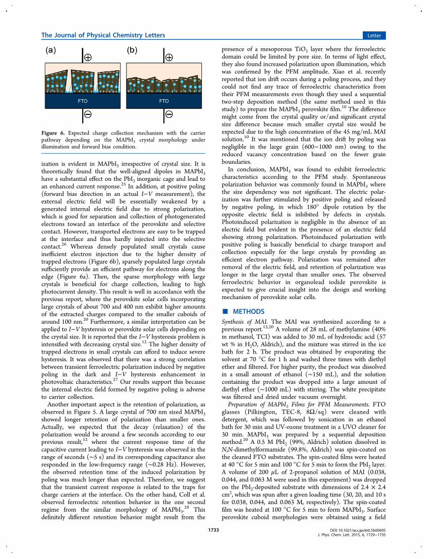
ization is evident in MAPbI3 irrespective of crystal size. It istheoretically found that the well-aligned dipoles in MAPbI3have a substantial effect on the PbI3 inorganic cage and lead toan enhanced current response.25 In addition, at positive poling(forward bias direction in an actual I−V measurement), theexternal electric field will be essentially weakened by agenerated internal electric field due to strong polarization,which is good for separation and collection of photogeneratedelectrons toward an interface of the perovskite and selectivecontact. However, transported electrons are easy to be trappedat the interface and thus hardly injected into the selectivecontact.26 Whereas densely populated small crystals causeinefficient electron injection due to the higher density oftrapped electrons (Figure 6b), sparsely populated large crystalssufficiently provide an efficient pathway for electrons along theedge (Figure 6a). Then, the sparse morphology with largecrystals is beneficial for charge collection, leading to highphotocurrent density. This result is well in accordance with theprevious report, where the perovskite solar cells incorporatinglarge crystals of about 700 and 400 nm exhibit higher amountsof the extracted charges compared to the smaller cuboids ofaround 100 nm.20 Furthermore, a similar interpretation can beapplied to I−V hysteresis or perovskite solar cells depending onthe crystal size. It is reported that the I−V hysteresis problem isintensified with decreasing crystal size.12 The higher density oftrapped electrons in small crystals can afford to induce severehysteresis. It was observed that there was a strong correlationbetween transient ferroelectric polarization induced by negativepoling in the dark and I−V hysteresis enhancement inphotovoltaic characteristics.27 Our results support this becausethe internal electric field formed by negative poling is adverseto carrier collection.Another important aspect is the retention of polarization, as
observed in Figure 5. A large crystal of 700 nm sized MAPbI3showed longer retention of polarization than smaller ones.Actually, we expected that the decay (relaxation) of thepolarization would be around a few seconds according to ourprevious result,12 where the current response time of thecapacitive current leading to I−V hysteresis was observed in therange of seconds (∼5 s) and its corresponding capacitance alsoresponded in the low-frequency range (∼0.28 Hz). However,the observed retention time of the induced polarization bypoling was much longer than expected. Therefore, we suggestthat the transient current response is related to the traps forcharge carriers at the interface. On the other hand, Coll et al.observed ferroelectric retention behavior in the one secondregime from the similar morphology of MAPbI3.
28 Thisdefinitely different retention behavior might result from the
presence of a mesoporous TiO2 layer where the ferroelectricdomain could be limited by pore size. In terms of light effect,they also found increased polarization upon illumination, whichwas confirmed by the PFM amplitude. Xiao et al. recentlyreported that ion drift occurs during a poling process, and theycould not find any trace of ferroelectric characteristics fromtheir PFM measurements even though they used a sequentialtwo-step deposition method (the same method used in thisstudy) to prepare the MAPbI3 perovskite film.
10 The differencemight come from the crystal quality or/and significant crystalsize difference because much smaller crystal size would beexpected due to the high concentration of the 45 mg/mL MAIsolution.10 It was mentioned that the ion drift by poling wasnegligible in the large grain (600−1000 nm) owing to thereduced vacancy concentration based on the fewer grainboundaries.In conclusion, MAPbI3 was found to exhibit ferroelectric
characteristics according to the PFM study. Spontaneouspolarization behavior was commonly found in MAPbI3 wherethe size dependency was not significant. The electric polar-ization was further stimulated by positive poling and releasedby negative poling, in which 180° dipole rotation by theopposite electric field is inhibited by defects in crystals.Photoinduced polarization is negligible in the absence of anelectric field but evident in the presence of an electric fieldshowing strong polarization. Photoinduced polarization withpositive poling is basically beneficial to charge transport andcollection especially for the large crystals by providing anefficient electron pathway. Polarization was remained afterremoval of the electric field, and retention of polarization waslonger in the large crystal than smaller ones. The observedferroelectric behavior in organolead iodide perovskite isexpected to give crucial insight into the design and workingmechanism of perovskite solar cells.
■ METHODSSynthesis of MAI. The MAI was synthesized according to aprevious report.12,20 A volume of 28 mL of methylamine (40%in methanol, TCI) was added to 30 mL of hydroiodic acid (57wt % in H2O, Aldrich), and the mixture was stirred in the icebath for 2 h. The product was obtained by evaporating thesolvent at 70 °C for 1 h and washed three times with diethylether and filtered. For higher purity, the product was dissolvedin a small amount of ethanol (∼150 mL), and the solutioncontaining the product was dropped into a large amount ofdiethyl ether (∼1000 mL) with stirring. The white precipitatewas filtered and dried under vacuum overnight.Preparation of MAPbI3 Films for PFM Measurements. FTO
glasses (Pilkington, TEC-8, 8Ω/sq) were cleaned withdetergent, which was followed by sonication in an ethanolbath for 30 min and UV-ozone treatment in a UVO cleaner for30 min. MAPbI3 was prepared by a sequential depositionmethod.20 A 0.5 M PbI2 (99%, Aldrich) solution dissolved inN,N-dimethylformamide (99.8%, Aldrich) was spin-coated onthe cleaned FTO substrates. The spin-coated films were heatedat 40 °C for 5 min and 100 °C for 5 min to form the PbI2 layer.A volume of 200 μL of 2-propanol solution of MAI (0.038,0.044, and 0.063 M were used in this experiment) was droppedon the PbI2-deposited substrate with dimensions of 2.4 × 2.4cm2, which was spun after a given loading time (30, 20, and 10 sfor 0.038, 0.044, and 0.063 M, respectively). The spin-coatedfilm was heated at 100 °C for 5 min to form MAPbI3. Surfaceperovskite cuboid morphologies were obtained using a field
Figure 6. Expected charge collection mechanism with the carrierpathway depending on the MAPbI3 crystal morphology underillumination and forward bias condition.
The Journal of Physical Chemistry Letters Letter
DOI: 10.1021/acs.jpclett.5b00695J. Phys. Chem. Lett. 2015, 6, 1729−1735
1733

emission scanning electron microscope (FE-SEM, JSM-7600F,JEOL). XRD patterns were measured by a HP-Thin Film XRDsystem (D8 Advance for high power, Bruker Corporation)using a turbo X-ray source of 18 kW with a scan rate of 2°min−1.PFM Measurement. The AFM-based investigations were
carried out using a XE-100 AFM (Park Systems). Theferroelectric polarization of the halide perovskite samples wasconfirmed by PFM. A lock-in amplifier (Stanford ResearchSystems SR830) was used to detect the piezoresponse signalequipped with conductive Pt/Cr-coated silicon tips (springconstant of 3 N/m), operating in contact mode for imaging oftopography and relative polarization by PFM. Samples werebasically kept in the dark before measuring without anypretreatment. For ferroelectric-induced dipole orientationmeasurements, a poling voltage of +3 or −3 V was applied tothe tip to align the dipoles in a single direction. Afterward, thePFM signal was measured. The deflection of the cantilever wasset to 30 nN, and the scanning rate was 0.5 Hz. The PFMmeasurement was conducted at room temperature in ambientair with 20% humidity. The sample scanning area was 5 × 5μm2 for 700 and 400 nm sized perovskite cuboids and 2 × 2μm2 for the 100 nm sized perovskite cuboids sample. A white-light point source (50000 lx) with a light guide GS6-1000Fintegrated with the AFM system was used to detect light-induced polarization.
■ AUTHOR INFORMATIONCorresponding Authors*E-mail: [email protected] (S.-W.K.).*E-mail: [email protected] (N.-G.P.).Author Contributions⊥H.-S.K., S.K.K., and B.-J.K. contributed equally to this work.NotesThe authors declare no competing financial interest.
■ ACKNOWLEDGMENTSThis work was supported by the National Research Foundationof Korea (NRF) grants funded by the Ministry of Science, ICT& Future Planning (MSIP) of Korea under Contracts NRF-2010 -0014992 , NRF-2012M1A2A2671721 , NRF-2012M3A7B4049986 (Nano Material Technology Develop-ment Program), and NRF-2012M3A6A7054861 (GlobalFrontier R&D Program on Center for Multiscale EnergySystem). H.-S.K is grateful for the Global Ph.D. Fellow Grantfunded by NRF. S.-W.K. acknowledges financial support by theBasic Science Research Program (2009-0083540) through theNational Research Foundation (NRF) of Korea Grant fundedby the Ministry of Science, ICT & Future Planning.
■ REFERENCES(1) Kim, H.-S.; Lee, C.-R.; Im, J.-H.; Lee, K.-B.; Moehl, T.;Marchioro, A.; Moon, S.-J.; Humphry-Baker, R.; Yum, J.-H.; Moser, J.E.; et al. Lead Iodide Perovskite Sensitized All-Solid-State SubmicronThin Film Mesoscopic Solar Cell with Efficiency Exceeding 9%. Sci.Rep. 2012, 2, 591.(2) Lee, M. M.; Teuscher, J.; Miyasaka, T.; Murakami, T. N.; Snaith,H. J. Efficient Hybrid Solar Cells Based on Meso-SuperstructuredOrganometal Halide Perovskites. Science 2012, 338, 643−647.(3) Burschka, J.; Pellet, N.; Moon, S.-J.; Humphry-Baker, R.; Gao, P.;Nazeeruddin, M. K.; Gratzel, M. Sequential Deposition as a Route toHigh-Performance Perovskite-Sensitized Solar Cells. Nature 2013,499, 316−319.
(4) Liu, M.; Johnston, M. B.; Snaith, H. J. Efficient PlanarHeterojunction Perovskite Solar Cells by Vapour Deposition. Nature2013, 501, 395−398.(5) Zhou, H.; Chen, Q.; Li, G.; Luo, S.; Song, T.-b.; Duan, H.-S.;Hong, Z.; You, J.; Liu, Y.; Yang, Y. Interface Engineering of HighlyEfficient Perovskite Solar Cells. Science 2014, 345, 542−546.(6) National Renewable Energy Laboratory Best Research-CellEfficiencies. http://www.nrel.gov/ncpv/images/efficiency_chart.jpg(2015).(7) Stranks, S. D.; Eperon, G. E.; Grancini, G.; Menelaou, C.;Alcocer, M. J. P.; Leijtens, T.; Herz, L. M.; Petrozza, A.; Snaith, H. J.Electron−Hole Diffusion Lengths Exceeding 1 Micrometer in anOrganometal Trihalide Perovskite Absorber. Science 2013, 342, 341−344.(8) Xing, G.; Mathews, N.; Sun, S.; Lim, S. S.; Lam, Y. M.; Gratzel,M.; Mhaisalkar, S.; Sum, T. C. Long-Range Balanced Electron- andHole-Transport Lengths in Organic−Iorganic CH3NH3PbI3. Science2014, 342, 344−347.(9) Kim, H.-S.; Mora-Sero, I.; Gonzalez-Pedro, V.; Fabregat-Santiago,F.; Juarez-Perez, E. J.; Park, N.-G.; Bisquert, J. Mechanism of CarrierAccumulation in Perovskite Thin-Absorber Solar Cells. Nat. Commun.2013, 4, 2242.(10) Xiao, Z.; Yuan, Y.; Shao, Y.; Wang, Q.; Dong, Q.; Bi, C.;Sharma, P.; Gruverman, A.; Huang, J. Giant Switchable PhotovoltaicEffect in Organometal Trihalide Perovskite Devices. Nat. Mater. 2015,14, 193−198.(11) Juarez-Perez, E. J.; Sanchez, R. S.; Badia, L.; Garcia-Belmonte,G.; Kang, Y. S.; Mora-Sero, I.; Biszuert, J. Photoinduced GiantDielectric Constant in Lead Halide Perovskite Solar Cells. J. Phys.Chem. Lett. 2014, 5, 2390−2394.(12) Kim, H.-S.; Park, N.-G. Parameters Affecting I−V Hysteresis ofCH3NH3PbI3 Perovskite Solar Cells: Effects of Perovskite Crystal Sizeand Mesoporous TiO2 layer. J. Phys. Chem. Lett. 2014, 5, 2927−2934.(13) Bertoluzzi, L.; Sanchez, R. S.; Liu, L.; Lee, J.-W.; Mas-Marza, E.;Han, H.; Park, N.-G.; Mora-Sero, I.; Bisquert, J. Cooperative Kineticsof Depolarization in CH3NH3PbI3 Perovskite Solar Cells. EnergyEnviron. Sci. 2015, 8, 910−915.(14) Nuraje, N.; Su, K. Perovskite Ferroelectric Nanomaterials.Nanoscale 2013, 5, 8752−8780.(15) Frost, J. M.; Butler, K. T.; Brivio, F.; Hendon, C. H.; VanSchilfgaarde, M.; Walsh, A. Atomistic Origins of High-Performance inHybrid Halide Perovskite Solar Cells. Nano Lett. 2014, 14, 2584−2590.(16) Liu, S.; Zheng, F.; Koocher, N. Z.; Takenaka, H.; Wang, F.;Rappe, A. M. Ferroelectric Domain Wall Induced Band Gap Reductionand Charge Separation in Organometal Halide Perovskites. J. Phys.Chem. Lett. 2015, 6, 693−699.(17) Butler, K. T.; Frost, J. M.; Walsh, A. Ferroelectric Materials forSolar Energy Conversion: Photoferroics Revisited. Energy Environ. Sci.2015, 8, 838−848.(18) Kutes, Y.; Ye, L.; Zhou, Y.; Pang, S.; Huey, B. D.; Padture, N. P.Direct Observation of Ferroelectric Domains in Solution-ProcessedCH3NH3PbI3 Perovskite Thin Films. J. Phys. Chem. Lett. 2014, 5,3335−3339.(19) Gottesman, R.; Haltzi, E.; Gouda, L.; Tirosh, S.; Bouhadana, Y.;Zaban, A. Extremely Slow Photoconductivity Response ofCH3NH3PbI3 Perovskites Suggesting Structural Changes underWorking Conditions. J. Phys. Chem. Lett. 2014, 5, 2662−2669.(20) Im, J.-H.; Jang, I.-H.; Pellet, N.; Gratzel, M.; Park, N.-G. Growthof CH3NH3PbI3 Cuboids with Controlled Size for High-EfficiencyPerovskite Solar Cells. Nat. Nanotechnol. 2014, 9, 927−932.(21) Dubourdieu, C.; Bruley, J.; Arruda, T. M.; Posadas, A.; Jordan-Sweet, J.; Frank, M. M.; Cartier, E.; Frank, D. J.; Kalinin, S. V.;Demkov, A. A.; et al. Switching of Ferroelectric Polarization inEpitaxial BaTiO3 Films on Silicon without a Conducting BottomElectrode. Nat. Nanotechnol. 2013, 8, 748−754.(22) Gupta, M. K.; Lee, J.-H.; Lee, K. Y.; Kim, S.-W. Two-Dimensional Vanadium-Doped ZnO Nanosheet-Based Flexible DirectCurrent Nanogenerator. ACS Nano 2013, 7, 8932−8939.
The Journal of Physical Chemistry Letters Letter
DOI: 10.1021/acs.jpclett.5b00695J. Phys. Chem. Lett. 2015, 6, 1729−1735
1734

(23) Jesse, S.; Rodriguez, B. J.; Choudhury, S.; Baddorf, A. P.;Vrejoiu, I.; Hesse, D.; Alexe, M.; Eliseev, E. A.; Morozovska, A. N.;Zhang, J.; et al. Direct Imaging of the Spatial and Energy Distributionof Nucleation Centres in Ferroelectric Materials. Nat. Mater. 2008, 7,209−215.(24) Lee, J. H.; Shin, R. H.; Jo, W. Polarization Switching andRelaxation Dynamics of Bismuth Layered Ferroelectric Thin Films:Role of Oxygen Defect Sites and Crystallinity. Phys. Rev. B 2011, 84,094112.(25) Zheng, F.; Takenaka, H.; Wang, F.; Koocher, N. Z.; Rappe, A.M. First-Principles Calculation of the Bulk Photovoltaic Effect inCH3NH3PbI3 and CH3NH3PbI3−xClx. J. Phys. Chem. Lett. 2015, 6, 31−37.(26) Yuan, Y.; Reece, T. J.; Sharma, P.; Poddar, S.; Ducharme, S.;Gruverman, A.; Yang, Y.; Huang, J. Efficiency Enhancement in OrganicSolar Cells with Ferroelectric Polymers. Nat. Mater. 2011, 10, 296−302.(27) Chen, H.-W.; Sakai, N.; Ikegami, M.; Miyasaka, T. Emergence ofHysteresis and Transient Ferroelectric Response in Organolead HalidePerovskite Solar Cells. J. Phys. Chem. Lett. 2015, 6, 164−169.(28) Coll, M.; Gomez, A.; Mas-Marza, E.; Almora, O.; Garcia-Belmonte, G.; Campoy-Quiles, M.; Bisquert, J. Polarization Switchingand Light-Enhanced Piezoelectricity in Lead Halide Perovskites. J.Phys. Chem. Lett. 2015, 6, 1408−1413.
The Journal of Physical Chemistry Letters Letter
DOI: 10.1021/acs.jpclett.5b00695J. Phys. Chem. Lett. 2015, 6, 1729−1735
1735