final report - workshop on failure and uncertainty … · workshop on failure and uncertainty in...
TRANSCRIPT

National Science Foundation
Workshop on
Failure and Uncertainty in Mixed-Signal Circuits and Systems
Arlington, Virginia
July 8-9, 2010 Principal Investigators: Ralph Cavin, William Joyner, David Yeh Semiconductor Research Corporation Program Manager: Andreas Weisshaar National Science Foundation Division Director: Robert Trew National Science Foundation Steering Committee: Andreas Cangellaris
University of Illinois at Urbana-Champaign
Ramesh Harjani University of Minnesota
Sule Ozev Arizona State University

Report from a National Science Foundation Workshop on Failure and Uncertainty in Mixed-Signal Circuits and Systems Arlington, Virginia July 8-9, 2010
PREFACE
This report summarizes the findings of an NSF Workshop on Failure and Uncertainty in Mixed-Signal Circuits and Systems, held July 8-9, 2010, in Arlington, Virginia. The objective of the workshop was to develop an outline of research needs for failure-resistant electronic mixed-signal circuits and systems to insure sustained and increased reliability in health-related, transportation (including automotive and aerospace), high performance computing, and energy-sustainable systems. Ralph Cavin, David Yeh, and William Joyner of the Semiconductor Research Corporation were the investigators, and Andreas Cangellaris (University of Illinois at Urbana-Champaign), Sule Ozev (Arizona State University), and Ramesh Harjani (University of Minnesota) formed a steering committee. Andreas Weisshaar was the NSF program manager. Other participants are listed at the end of this report. The format of the workshop included presentations and panel discussions from academic and industry participants, breakout sessions, and the outlining of a report recommending research directions and next steps. The initial workshop session highlighted current activities in this space, and was followed by five sessions that break down the hierarchy into topical areas. Each of these five sessions consisted of speakers with a session chair moderating the fifteen minute discussion period. On the second morning, the participants divided into two groups to synthesize the discussion into key research areas from each session, and each group’s findings were presented to all of the participants at the end of the morning. The agenda may be found at the end of the report.
The principal investigators would like to thank NSF, the steering committee, and all the participants for their contributions to the workshop and this report.
INTRODUCTION
Electronic system design is at a crossroads. For both large infrastructure-supporting systems and small embedded systems for medical and other applications, the price of failure is extremely high. Since many aspects of daily life – communication, health, transportation, shelter, energy use, etc. – depend on such systems, increasing their reliability would have not only technical merit, but a broader impact across society. Fundamental new advances in techniques for developing systems immune from failure would quickly be adopted in the marketplace, and could be both transformative and translational.
One cause of reduced reliability is the increasing probability of device failure as feature sizes of integrated circuits are reduced. However, with the increased presence of analog circuits and components as parts of systems as well as the increased 3D integration density, other reliability concerns arise. Besides the problem of reduced device reliability and increased parameter uncertainty, the complicated coupling between densely integrated components, circuits, packaging and sub-systems is often too complex to be fully considered in the design. Failure of such systems may not be of the traditional pass/fail nature and might be caused by either design errors (or poor designs) or operational conditions. Instead, for mixed-signal components as well as for systems at the application level, there is more concern with graceful degradation, recovery from transient and permanent errors, and robust behavior at the system level. This suggests that an integrated approach incorporating all levels of the design hierarchy is necessary to provide reliability to the system user. Techniques that emphasize probabilistic/stochastic design might be appropriate. Furthermore, this approach is apparent in multiple application spaces, including high performance computing and communications, electronics for aerospace and other transportation systems, and healthcare applications. As these application spaces suggest, reliability needs to encompass digital, analog, and RF design across a wide range of operating conditions as well as failure modes.
Digital Reliability. Failure resistance for digital circuits and systems has been an important focus area for industry, university, and government research efforts for many years. Recently, NSF supported a study in this area, with several workshops and a report. These workshops on cross-layer reliability, focusing on digital systems, were conducted by the Computing Community Consortium and held March 26-27, 2009; July 8-9, 2009; and October 29-30, 2009. Information about the meetings is available at www.relxlayer.org .

Analog/Mixed-Signal System and Circuit Reliability. Electronics is no longer a digital world; estimates today indicate that 75% of chips produced have analog content. In addition, electronics for medical, transportation, and aerospace applications involve significant mixed-signal components and are particularly important areas for reliability assurance. A key aim of this workshop was to develop an outline of research needs for failure-resistant electronic mixed-signal circuits and systems to insure sustained and increased reliability in health-related, transportation (including automotive and aerospace), high performance computing, and energy sustainable systems. Describing these research challenges for design of failure resistant analog/mixed signal systems and circuits, as well as infrastructure and tools needed, complements the work of the ongoing cross-layer reliability study sponsored by NSF through the Computing Community Consortium mentioned above.
Multiple test, validation and verification steps are needed to ensure that a design achieves its desired capabilities. If hardware errors are found, they should be corrected prior to fabrication, before they are irrecoverable. It is commonly accepted that the earlier these issues are corrected, the cheaper the cost – the cost of respinning a design or debugging the silicon is much higher than correcting the design prior to fabrication. It is critical from a cost standpoint to send a correct design to fabrication.
The need to integrate analog functions and digital computing together has been reflected in the growth of mixed-signal design. There are now incredibly large designs that have extensive compute capability at a low cost and power capability. Modern system requirements are continually evolving as the ICs are used in more diverse domains. Formerly, electronics was focused in consumer products, communications, and computing systems. In the last 10 years, electronics have increased their footprint in such diverse areas such as medical, automotive, and power infrastructure. These ICs have allowed products in these areas to add capabilities and reduce costs.
With this trend of electronics utilization in such varied environments, new demands have appeared. The overall functional, performance, reliability, and even lifetime requirements, expressed at the system level, must be reflected in the IC design process. Conversely, an increasing variety of characteristics at the circuit level must percolate up to the system design process. Building enough safety margin into a design to address extended lifetime requirements today raises significant questions:
How does one test the system to guarantee that the design margin is sufficient to meet the implementation goal? Other environments require proof that the system will be functional over the appropriate period.
How does one address the lifetime requirement and still maintain the cost and performance benefit that the IC design was targeting?
The growth of the IC market has led to innovative applications, which introduced new design requirements. The key challenge will be to capture those innovations to allow for the validation success for full designs to continue in advanced process nodes.
The increased presence of analog and mixed-signal circuits along with increased scaling and system complexity requires changes to the formal reliability certification and qualification infrastructure that is currently applied to integrated circuits and systems. Reliability test methods and prediction methodologies will need to comprehend a broader variety of failure mechanisms, with appropriate time-dependent models that reflect the failure characteristics of these complex systems. System topology models need to extend beyond simple series / parallel / k-out-of-n / combined series-parallel to accommodate combined analog-digital blocks and combined hardware-software systems. These enhancements must also be applied to the functional safety standards used for electronic systems, and to industry specific standards (such as those for automotive applications). Importantly, research is needed beyond the basic understanding of failure mechanisms to develop accurate and efficient models that can be implemented in cost-effective certification and qualification methodologies.
Up and Down the Hierarchy. The target of design is to conceive reliable and robust circuits and systems that can perform their intended functionality over the intended lifetime of the product, either by avoiding failures through anticipation, or by having some built-in mechanisms to survive and recover from failures or - at worse - to gracefully degrade allowing the user to take action. Considering the relentless progress in fabrication technology, both for the semiconductor technology itself as well as the “system” technology (packaging, bonding, 3D integration, etc.), the physical sources of variation and failure are not always well understood and often not well characterized for the technology that designers have to use or will be using. This creates uncertainty. In addition,

since most of the underlying physical phenomena are either deterministic but with statistical spread on their magnitude or are statistical in their occurrence itself or depend on unknown external factors or usage patterns, designers must cope with this stochastic nature of the problems.
One of the challenges of design is therefore the propagation of this stochastic and uncertain information up and down the design hierarchy in order to be able to design reliable systems. First, this implies that reliability requirements need to be propagated down the hierarchy to the individual blocks and circuits. Second, this implies that the information of the physical phenomena, which is typically situated at the technology and device level, must be propagated upwards to analyze the effect on the performance of circuits, building blocks and entire systems, to the extent needed to assess reliability of functionality and performance. The amount of information that is needed at any level, however, depends on the measures taken towards reliability at higher levels, and vice versa decisions taken at any level to improve reliability depend on information about failure probabilities propagated from lower levels. The integration of reliability into a hierarchical design flow is therefore a challenging task, which is further complicated by the ambiguity about what precisely contributes a system failure. For the case of analog and mixed-signal circuits, most phenomena affect circuit performance parametrically but not necessarily alter functionality.
Propagation of information and constraints up and down the hierarchy is a key part of any reliability methodology. Propagation of statistical and uncertain information poses several research challenges. Any correlations between phenomena need to be considered to get realistic instead of overestimated results. Error masking is another problem, especially in systems with much redundancy and/or reconfigurability. In order to simulate or analyze such systems, computational complexity is a huge challenge due to: 1) the sheer complexity of the targeted circuits and systems, often with several local and global control/tuning loops, necessitating hierarchical approaches, 2) the stochastic nature of the phenomena, requiring efficient ways to deal with stochastic variations, and 3) the time-dependent nature of some phenomena requiring dynamic instead of only static techniques. Phenomena that rely on external factors such as usage patterns also need to consider the probability of different usage scenarios. Fundamental research is therefore needed to develop techniques that can balance compute efficiency and accuracy in the presence of statistical and uncertain data sets, and that can efficiently propagate information up and down a design hierarchy.
MIXED-SIGNAL SYSTEM APPLICATIONS AND RELIABILITY CONSTRAINTS
The use of electronics in general purpose computing and communication systems is already highly pervasive. Much of the credit for this goes to “Moore’s Law” where the scaling of the process dimensions enables more functionality to be available at the same cost for each successive manufacturing node. In each of these applications the requirements for integrated circuit reliability are such that occasional failures were tolerated or were not exceedingly difficult to meet. Examples of such tolerated failures include garbled phone transmissions and personal computer lockups.
Embedded computing applications are gaining increasing use in platforms such as automotive, healthcare, aerospace, and energy systems. These applications have different characteristics that affect the way electronic systems fail and the degree of user tolerance for such failures. In the case of automotive and aerospace, there are extreme temperature variations that can affect reliability. For healthcare applications where devices are implanted in-vivo, the need for ultra-low power operation for extended periods makes reliable operation more difficult. Each of these application areas consist of highly integrated electronic components with interfaces to the physical world and so have both digital and analog functions. These mixed-signal applications are the emphasis of this workshop and the presentations in this session.
With many mixed-signal systems, the failure modes of the devices are not uniform in nature and cannot be classified into strictly “pass” and “fail” buckets. The failure modes may be caused by design errors (or poor designs) or operating conditions and may be either transient or permanent. If systems are to be designed with graceful degradation in mind then how the application degrades and under what conditions it happens can be an extremely difficult design problem. Besides the problem of reduced device reliability and increased parameter uncertainty, the coupling between densely integrated components, circuits, packaging and sub-systems is often too complex to be fully considered during the design phase, causing additional uncertainty in the final system.

Two applications that require extreme reliability include autonomous vehicle systems and implanted medical devices. The current automotive generation already includes tens of microcontrollers for engine control, ABS brakes, HVAC, etc. Some estimates show that roughly one third of the current cost of an automobile is electronics. This percentage is only likely to grow with increased use of electronics in the future. With the higher levels of integration possible combined with the desire to remain connected at all times, we are likely to see wireless radios everywhere to connect the car to the sensors on the road, to media, between cars, etc. In the near future, the increased integration levels allowed by Moore’s law will allow the electronics to be sufficiently “smart” for autonomous vehicles to become part of our daily life. In fact, extensive use of electronics will be the necessary ingredient to make autonomous cars possible, to accommodate the increased vehicular density on roads without grid lock, to keep occupants safe and to reduce accidents. It may be possible for occupants to relax while the car drives to/from home or work. However, before ceding driving control to computers, reliability assurance is needed.
A closer look at the implantable medical devices application reveals a stronger reliability requirement than mainstream computing applications as well as a different emphasis in design optimization. Low power operation is the primary goal, then system form-factor, and then performance. Many of these devices perform life-sustaining activities and must do so for longer duration than mainstream ICs in a harsh environment that might have large variations over time. Some of the environmental concerns are mechanical shock and stress, electromagnetic interference, cancer radiotherapy, and cosmic radiation. The power available for such devices could be in the single digit micro-watt levels with operating voltages around or below one volt.
Medical devices are generally fabricated in a semi-custom IC process. Process modifications for current products include threshold shifts and thicker oxides to battle leakage for low power operation, lightly doped drains to minimize aging effects, custom designed transistors to aid in radiation immunity and full custom digital gates designed for low power operation. Of course, any process modification requires a change to the transistor models; this is typically done by the IC design engineers in an iterative process. Coupled with the need to characterize and qualify the IC process, the effort to adopt new process nodes is not a simple undertaking. Implantable ICs will be used in products that will be for sale for many years, requiring the IC process to be available for a longer duration than common mainstream IC processes. A strong relationship with an IC vendor is mandatory for medical device manufacturers to design appropriate ICs.
In addition to the design considerations, much effort is put into screening the implantable ICs. For economic reasons, manufacturers of commercial off the shelf parts cannot provide the necessary testing to ensure the level of screening required for medical applications; it would just take too long and cost too much. Tests include baking the ICs while under power and overvoltage stress to force failure of marginal parts. These procedures may actually reduce the failure-free operating time of the IC as they may transition parts from a 'good' point of the distribution curve to a 'marginal' point and still pass the manufacturing tests. Another common test is IDDQ testing. This procedure is ideal for implantable ICs as measured against ultra low quiescent currents, faulty parts stand out clearly. Any effort to reduce the test burden by increasing design or manufacturing reliability would not only create more reliable parts, but would reduce the cost of the final part.
With the above design considerations, there is little control over the operational environment of implantable devices. They must operate correctly under mechanical shock and stress, electromagnetic interference, cancer radiotherapy, cosmic radiation, etc. These environmental hazards can result in bit flips in SRAM and logic or threshold modification in analog circuits. With all the design, manufacturing, test and environmental constraints, implantable ICs are often required to perform without failure for over 10 years. Unit replacement due to an IC or system failure will place the end user at a great risk and cannot be viewed as a primary path of resolution. To this end, reliable operation is of paramount importance.
Rather than thinking of variability as “the enemy” it may be possible to develop radical new architectures which in fact rely on lower-level variability to realize higher-level functionality. Intentional randomness is already inserted in a variety of systems to shape spectrums or enhance communication-channel capacity. To enable a variability-aware approach, models are first needed to accurately predict variability and aging distributions or boundaries. New design methodologies and tool enablements are then needed to allow for quick simulation of these new variability-aware architectures. Finally, new circuit and system architectures must be developed which can leverage the randomness to achieve new functionality or lower power consumption at lower cost.

Large digitally-assisted or self-healing systems will have the capability to overcome a certain amount of lower-level (i.e., component-level) failures. These systems essentially have a certain reconfigurability or healing range which needs to be “budgeted” between process, voltage, temperature, and aging effects. Test, therefore, needs to take this into account and develop straightforward methods to quantify the robustness of the part and only promote parts with a sufficient reconfigurability budget to work properly in the field. Additionally, as these systems become more reconfigurable, the number of states to be tested grows disproportionately; hence, new approaches are required to guarantee sufficient test coverage while not allowing the test time to become unbounded.
Another challenge is both to determine which parameters should be repaired to achieve overall system reliability and to determine the best overall approach. The fundamental trade-offs between reliability, energy efficiency and performance in a self-repairing system are of great interest. Although redundancy, trimming and calibration are known techniques, a challenge is to determine the best overall approach to self-repair. In fact, the optimum solution may well be a combination of these approaches. The cost of self-repair in terms of energy, power and performance should be also considered.
Self-repair can also be seen as the reversal of degradation. An alternative and complimentary approach is to directly reverse device-degradation. The challenge is to discover new ways to reverse degradation by temporarily or permanently modifying the device environment. As an example, NBTI can be reversed by the application of particular gate-voltage waveform. This approach involves research in device degradation mechanisms as well as new circuit techniques.
Key needs:
• Identify and understand models failure mechanisms and requirements of each application domain
• Design tools that cross traditional domain boundaries (e.g. chip-package, package-board, …)
• Design methodologies, techniques, and tools to drive yield-based design
• Design tools and methods to increase designer productivity and decrease test time
• Architectures which leverage randomness and variability
RELIABLE MIXED-SIGNAL DEVICES AND CIRCUITS
Future mixed-signal electronic systems will contain a large portion of calibration and correction circuitry, designed to absorb both production variability and parameter drift over life time. This leads to an increase in the number of possible system states and complex interaction possibilities between the respective states and drift effects. In this context, we see a significant challenge in attaining proper production test coverage within reasonable time and power, and justifiable cost. Especially for long-term drift effects and their compensation methods, it is unclear how one can exercise all relevant states that will be seen during the device’s lifetime. Some conditions may only be seen after the true physical parameter shifts (e.g. CMOS threshold voltage shifts due to NBTI) have occurred. Consequently, there is a need to assess the required test coverage for a system that is expected to drift substantially after production test. It is unclear whether the suitable production test methods will need to be fully customized to a particular system, or if there are commonalities and general solutions that may be amenable to automation (in the spirit of automatic test vector generation). The same issue extends into design time verification and validation, with the added challenges of handling vastly different time scales and multi-physics phenomena in the simulation platform. As result, there is also a pressing need to develop tools and methodology for fault and failure analysis at design time.
Process variability is one major source of uncertainty and is becoming an increasingly challenging issue with process scaling. Such variations can arise from the stochastic nature of device threshold voltages and device dimensions. Other sources of variability depend on circuit operation and the external environment. Examples include NBTI in PMOS devices, temperature variations, performance degradation in external components, and supply variations.

Mixed signal circuits and architectures are often designed to operate correctly across worst case process corners and operating conditions. This can result in a pessimistic design, and utilize the process technology in a sub-optimal way. Additionally, over-design is often required to compensate for aging effects mentioned above, since these can cause the performance to drift or change over time.
To combat variability in future systems, new design approaches are required that are capable of self-adapting to compensate for the above effects. The goal is to make it unnecessary to design for worst-case process corners, thereby better exploiting the performance that is available from the process. Techniques that allow for controlling performance in the presence of environmental variations, such as self-adapting and self-healing designs, as well as the use of redundancy need further research. As systems become increasingly complex, and include a variety of hybrid sub-systems, techniques that compensate for change at a global level, while considering diverse variation mechanisms that can exist at the sub-system and component level also need further investigation.
One recurring theme discussed in the workshop was the need for better understanding and characterization of reliability and variability mechanisms and the corresponding need for faithful and tractable design models. In current practice, models of things such as devices, packages, components, and IP may not exist or may be out-of-date. Furthermore, the model fidelity may not be high enough for the intended use.
Achieving first time success in integrated circuit design relies on efficient and accurate models for the devices, packages, external components and systems. While many of these models exist for today's technologies and applications, they fall short of present and future needs for applications requiring high reliability and which are designed in processes with high variability. These challenges must be addressed by developing models that predict the variability over time and process. Additionally, these models must be correlated to measured devices with accelerated life testing. Designers need efficient mechanisms to correlate the simulation of degradation of performance over time and determine how this correlates to real device degradation as a function of time and environment. This accurate and efficient simulation and modeling capability is needed at all levels of abstraction including devices, circuits, systems and applications. These models and simulation constructs must be part of the standard design flow that digital, analog and mixed-signal, and system-level designers currently use.
A list of possible failure mechanisms of mixed signal integrated circuits is extensive. It includes unrecoverable failures such as early life failure (ELF)[Con88] due to gate oxide defects that cause a catastrophic failure shortly after production test and burn in, and time dependent dielectric breakdown (TDDB) [Che85] of gate oxide layer that occurs over a longer life time. TDDB failure is believed to be due to the formation of a percolation path of defects across the oxide which ultimately leads to destructive breakdown. Excessive exposure to radiation can also cause catastrophic failures.
Recoverable failures present in mixed signal integrated circuits include a latch-up [Tro86] due to parasitic structures that continue to be present in mixed signal systems implemented using CMOS and bipolar technologies, and single event upset (SEU) due to alpha particles from metallization and packaging, high-energy cosmic rays and the secondary radiation induced from the interaction of cosmic ray neutrons and boron which is used as a p-type dopant and implant species in silicon and is also used in BPSG (boro-phospho silicate glass) dielectric layers. Although SEUs mostly affect memories (DRAMs and SRAMs) and sometimes logic circuits in scaled technologies, mixed signal circuits can also be affected. Another emerging device reliability concern is random telegraphy noise (RTN), which is currently a concern for SRAMs.
There are also aging effects that alter circuit properties over time due to changes of characteristics of devices temperature in the circuit. These include hot carrier injection (HCI) in MOS and bipolar transistors, more recently identified negative bias temperature instability (NBTI) in CMOS, and electro-migration in metal lines and contacts that can change resistances over time. Migration of metal under mechanical stress can also make resistances of metal lines, contacts and vias vary with time. NBTI is due to the injection of holes into the gate oxide, which break Si-H bonds at the oxide interface and create interface traps. HCI and NBTI can change transconductance and threshold voltage as well as low-frequency noise characteristics of devices. NBTI-induced p-channel device degradation will have a significant impact on minimum operation voltage of analog and mixed-signal circuits. Exposure to radiations in space and during imaging for medical and security checks also alters device

characteristics over time in mixed signal systems. Similarly, positive bias temperature instability (PBTI) is another aging effect to be considered.
Key needs:
Circuit architectures with periodic self test to ensure long term reliability
Circuits to correct/calibrate/test on-chip parameters
High frequency circuits that can be reliably and predictably designed
Circuits that efficiently correct/calibrate end-of-roadmap CMOS devices
Circuits in both digital and analog domain that guarantee test coverage
Circuits for providing reliable references
Techniques to mitigate noise increases due to device degradation
System architecture for reliability
Full system level simulation capability with component reliability included
MIXED-SIGNAL RELIABILITY TESTING AND VALIDATION
Fault models for latent defects. Fault models for mixed-signal subsystems (and systems) have been intensively researched in the last decade, with many models proposed by academia and industry but seemingly without reaching agreement on a subset of analog / mixed-signal faults to be tested for. Latent defects (structural defects whose impact is not immediately observable) affect mixed-signal reliability and pose even more difficult problems. During the lifetime of a device, due to wearout, these defects progress into more catastrophic fails and shorten the lifetime of the device significantly when compared with reliability-model based predictions. Such latent defects that significantly shorten the lifetime of a device should be monitored, detected and corrected by adaptation.
These defects include, among others, faults manifested due to environmental factors, stresses, and drifts during lifetime. State-of-the-art models for latent defects and faults tend to focus on individual devices (e.g. a single wire, a single transistor, interface between silicon and dielectric materials) where the physics is well understood, or very high level systems (e.g. entire automobiles, aircraft, packaged chips), with very little understanding of reliability models for the intermediate level of circuits and subsystems (e.g. converters, oscillators, comparators).
By nature, these latent defects manifest stochastically and maybe even intermittently, sometimes with minimal impact to device performance or unnoticeable impact (e.g. faults occurring during intervals when the mixed-signal subsystem outputs are not being used by the overall system functions), and sometimes with detrimental impact leading to failures. Stochastic detection methods, for both mixed-signal and even all-digital systems, need to be developed and verified experimentally for these systems.
A corollary of latent defects and stochastic detection is the requirement of guaranteeing mixed-signal system performance over a specified lifetime. Predictability is critical, both in commercial and defense applications, and needs to be updated during the device lifetime to take into account latent defect manifestation and impact. Prediction methods should lead to a more robust estimate of remaining lifetime, time before next maintenance or replacement.
Physical reliability models due to electromigration and oxide breakdown exist and have been verified. However, impact of wearout on device performance has typically been explored for digital circuits. While there may be similarities in the manifestation of wearout for digital and analog circuits, distinct operating conditions of analog devices may result in different wearout patterns. Fault models for latent defects including this varying nature of wearout for analog circuits are still lacking.
There are certainly approaches to developing fault models, detection methods and prediction methods. While data-oriented approaches are valid and have been frequently used as part of optimization algorithms to solve these problems in test and reliability, it is also desirable to understand the fundamental physical causes and

interactions (not just at device level but also at circuit and subsystem levels) that lead to faults or their manifestations at particular times. Fundamental scientific understanding is critical when technologies scale down or when a technology production lifetime is much shorter than system application lifetime in the field. This physical understanding also helps delineate the effects of hardware-oriented faults and failures from the effects of software-oriented faults and failures. The increasing programmability and software contents of integrated mixed-signal systems have led to reliability issues not foreseen in existing reliability models and studies.
Control for adaptive systems. Control, especially using feedback and automatic reconfiguration or calibration, is a classical method to guarantee performance of otherwise non-robust systems. Reliability-oriented control research poses an even more formidable challenge since these controls need to be exerted as functions of time, not just functions of system parameters. Periodic monitoring of system parameters over time is required and some level of controls needs to be built into system hardware and software, with attendant overhead considerations, to be activated as necessary. The variety of control mechanisms is bewildering but must not affect the mixed signal system performance when they are activated. These controls could be internal to the subsystem under consideration or from another subsystem within the overall system.
Feedback control could also lead to instability and even system failures due to oscillating responses. The stability requirement is paramount in mixed-signal systems and must be fully verified when control is implemented to ensure system reliability over time. The interaction between the control mechanisms, parametric drifts, environmental stresses, etc. must be understood or at least predicted well enough to provide sufficient margin to guarantee performance while avoiding instability.
Many existing self-calibrating systems (e.g. pipelined A/D converters, digitally calibrated image-reject receivers) use digital circuitry for self-calibration. When adaptation is performed across the system-architecture-circuit levels, software and digital as well as mixed-signal circuitry may be used to enable adaptation. In specific instances, software running on an available DSP may be used to implement a feedback control law that senses the system level workload, as well as its health and performs adaptation across the algorithm-architecture-circuit layers to reduce power consumption and maximize system lifetime. When such a DSP is not available, adaption must be performed by dedicated on-chip circuitry that must itself perform reliably in the presence of manufacturing and lifetime uncertainties. A key issue is that of designing an optimal nonlinear control law that guarantees an optimal or near-optimal solution (power, reliability) across a wide range of workloads and system health conditions. In addition, stability of the control mechanism must be ensured while allowing convergence to be achieved in a minimal number of steps. For post-manufacture tuning, the total tuning time must be minimized and of the same order as the time taken to test “static” systems today.
Built-in continuous monitoring and adaptation. Future “real-time” cyber-physical systems such as autonomous vehicles and mobile robots will experience large changes in workload through their day-to-day cycle of use as well as lifetime changes in performance (uncertainties) due to manufacturing imperfections, electrical wearout, thermal effects and aging. Any test approach for such systems must not only validate the correct operation of the system right after manufacture (i.e. its ability to compensate for manufacturing process variations across a range of workload conditions) but also validate that the system will be able to adapt correctly to changes in workload as well as lifetime changes in performance of the underlying devices in the field. Further, the testing performed right after manufacture should be low-cost and able to test adaptive systems at marginally more than the cost of testing current “static” designs. For in-field testing, built-in testing schemes must be used in such a way that the test results are resilient to uncertainties in the test hardware or software itself, both for parametric as well as catastrophic failures.
Where adaptation is concerned, a key objective is to reuse as much of the adaptation hardware for test/built-in test as possible. Such reuse of voltage/current adaptation mechanisms for example, presents key design challenges. When device performance degradation occurs due electrical or thermal stress, mechanisms that allow system lifetime to be extended by redistributing the stress conditions across the system modules must be incorporated into the design. In each case, any adaptation or tuning must be performed for system level performance metrics in a hierarchically integrated manner.
Reliability testing as qualification test of systems. For digital test the test coverage is well defined based on established fault models and accepted as general term in industry. For analog circuits however there are multiple definitions as a result of the lack of general fault models. Full test coverage using the weakest definition can be

counted as “powered up and tested one parameter of every sub-circuit,” but for the strongest definition as “every single transistor tested for all minimum and maximum conditions (like voltage, current, load, temperature etc)”. In the absence of well defined and conclusive fault models, it is common practice in analog device production to test the devices with respect to the specified performance.
Analog parameters can age over the lifetime of a product; this aging can show up as a defect, but also as a parametric shift. One solution to overcome the lifetime shortening effects is to build in redundancies and adaptive circuits which will compensate for the performance shift or take over the functionality of a defect subcircuit. It is obvious, that also these adaptive and redundant circuits will have the same aging effects than the circuit itself and will need to be tested as part of the production flow.
For production test there are two questions to be answered with the assumption made above:
1) Can the redundant and adaptive system components be tested to assure full functionality when the system ages and how will these components impact the performance? Furthermore, what is the test coverage for all conditions under which the device will perform?
2) How can a device be qualified if it includes adaptive circuitry?
Critical to answering the first question is to understand the aging effects, the control mechanism of the adaptive circuits and the time dependant load condition of the device. With this knowledge models can be developed predicting the device performance based on T0 test data.
For qualification tests, it will be essential to demonstrate that the device test setting will represent the normal specified use condition and that the stress test will verify the functionality of the redundancies and adaptive subsystems. Since the stress tests are typically determined late in the development cycle, a good predictive model will be required. Typically these predictions are based on simulations; in this case reliability simulations are necessary on top of the device simulations which require detailed simulation models. A precise reliability model for the different aging effects will also be required.
Production test coverage. There are multiple aspects to discuss when defining the production test coverage for analog devices. Already for non adaptive devices without any redundant subcircuits, it is difficult to have a commonly accepted definition of test coverage; for devices designed to compensate for aging effects, improving the reliability will become even more complex. Some aspects to take into consideration when defining the test coverage are
The load conditions might be adapted to improve the reliability during normal life time operation
Redundant subcircuits might need to have an independent test access
How can the specified performance based test results at T0 be predicted, and what kind of correction and correlations needs to be done?
Test coverage of device internal control loops for aging compensation
When using sensors to compensate for aging effects, how can the sensor be tested and predicted to be aging free?
One approach which could help is to adapt the test coverage and test strategy of digital circuits with testing for known and defined fail modes. Another approach would be to have sufficient guard band when testing at T0 to cover parametric shifts and use special test and stress conditions to activate aging effects impacting life failures.
Analog test coverage and DfT techniques have been discussed for many decades, however production test techniques repeated in publications still look immature. In the general discussion of production test coverage for analog devices these DfT techniques could be proven and introduced as a generally accepted alternative to performance-based test.
Designers sometimes try to include redundancies into the circuit for devices that fail often. Examples could include using multiple pads for ground and Vdd connections, and using multiple vias. While such techniques are generally ad-hoc and are subject to constraints on pin count and area, they make the testing process more challenging. A failing redundant part cannot be detected through performance-based testing alone. However, a failing redundant

part may shorten the lifetime of a device and may be indicative of a larger reliability problem. Test strategies to detect such failures are an area of need.
The lifetime of a device depends on the process, its features, and the operating conditions. While models exist to predict the wearout patterns of simple structures, these models could be extended to more complete circuit and system level operating conditions, incorporating notions such as bias currents and workloads.
Models and methods are necessary to predict the remaining lifetime of a circuit in-field as feedback is obtained from continuous monitoring schemes. Such models can be used to adapt the system with respect to varying wearout patterns of the circuit components, as well as re-distributing the workload.
These models can also be used to predict the initial lifetime of the device at production time. Strategies of either rejecting devices with short lifetimes or binning them with respect to lifetime may be possible using these models.
Key Needs:
Fundamental understanding of physical causes and interactions that lead to latent defects as technologies scale down
Effective built-in continuous monitoring and adaptation
Improved analog test coverage and DfT techniques
Models and methods to predict the remaining lifetime of a circuit at production and in-field
Precise reliability models for different aging effects
RELIABILITY AT DIFFERENT LEVELS OF ABSTRACTION.
“Reliability” of a system refers to the probability that the system’s performance meets its requirements over the lifetime of the system. These performance attributes are often determined by quality-of-service requirements and may include operating speed, power dissipation, availability, or others. Which performance attributes are critical will depend upon the applications that drive the system’s requirements. Uncertainty in the lifetime of the system is introduced due to variability and aging in the actual realization of the system and its components, as well as the operating environment.
Analog and mixed-signal systems rarely operate in isolation and are generally embedded into a larger system context ranging from heterogeneous mixed-signal components in a system-on-chip (SOC), to mixed-signal SOCs interconnected on a board, to large-scale interconnected systems. Present-day design flows and design automation methodologies over-specify analog mixed-signal components, require deterministic performance guarantees, employ overly conservative design metrics, and ignore inter-component interactions completely or model them very grossly. All of the above force the design of reliable systems to be built using reliable components that contain excessive design margins and come at a considerable overhead cost. Such design methodologies are unsustainable in the era of ever increasing system complexity and increasing variations/uncertainty at the component level. Next generation AMS design flows and design automation methodologies need to be built around the overarching philosophy that reliable systems can be built from unreliable components. This requires a framework within which system-level tradeoffs can be made in a robust manner in order to achieve system-level reliability with relaxed specification and optimal design of AMS components, in a manner akin to communications systems that deliver reliable data transmission through a series of imperfect and variable channel components by focusing on the goal of the entire system.
Engineers design complex systems iteratively. The system is designed at a high level of abstraction as a collection of subsystems, each of which is also described at that same high level. Each of the sub-systems is then refined by describing it at a more complete and detailed level of abstraction until a physical description is available and implemented. This iterative approach to designing systems has successfully permitted engineers to create extremely complicated integrated circuits, but it also creates new problems. Many reliability concerns only become quantifiable at the schematic and sometimes layout levels of abstraction. On the other hand, these concerns have system level implications. They may also be addressed more efficiently by making the appropriate

tradeoffs at various intermediate levels of abstraction in the design process. Techniques that require some degree of adaptation in order to improve reliability, for example, are better modeled at a level where efficient logic simulation can be done. However, the information that is required to diagnose, design, and optimize the performance and stability of adaptation techniques is typically available at a more detailed level of abstraction. In addition, modern SoCs are often designed with components from different vendors. How reliability information should be combined between sub-systems and across levels of abstraction requires the development of appropriate models and methods. It is important to be able to quantify the reliability of the overall system at multiple levels of abstraction and combine the individual reliability behaviors of the subsystems without overestimating (by double counting effects, for example) or underestimating (by masking effects, for example).
Most of the underlying physical phenomena that cause reliability degradation are either deterministic but with statistical spread on their magnitude, or are statistical in their occurrence itself, or depend on unknown external factors. Propagation of statistical and uncertain information across multiple subsystems and across different levels of design hierarchy poses significant additional challenges. In AMS circuits and systems, there is further ambiguity about what precisely affects the reliability of the system. Many reliability degradation phenomena rely on external factors such as operating environment or usage patterns, and the probability of these conditions needs to be considered. All of these statistical interactions need to be described and operated upon in a manner that is computationally affordable. The formulation of these descriptions needs to account for the ability of tools to handle such descriptions in a robust manner, as part of an automated design flow.
Fundamental research is therefore needed to develop AMS reliability design techniques that can balance computational efficiency and accuracy in the presence of statistical variability and degradation data. Reliability information needs to be formulated in a manner that can efficiently propagate up, down, and across a design hierarchy. A system-level approach to AMS design is essential, in order to successfully build reliable systems out of unreliable components.
Key needs:
• Addressing uncertainty introduced due to two major factors – environment and complexity – across multiple levels of abstraction
• Framework to analyze system-level reliability and derive relaxed specification of component reliability requirements
• Standardized models and methods to convey reliability information across levels of design hierarchy, or between different vendors providing components
• Methods to address voltage scaling in delivering mixed-signal performance in scaled technologies
• Statistical methods with affordable computational cost for use in automated robust design to deal with complexities between coupled heterogeneous system components
• Use of available transistor count to do more “intelligent” methods of error detection and recovery
• Architecture and logic design using stochastic techniques and statistical models of circuit behavior
• Test and verification for systems designed with these approaches
• Reliability information / models / metrics propagating up and down the system hierarchy (from process to devices to macrocircuits to chips to systems, and vice versa)
DESIGN FLOW AND TOOLS FOR MIXED-SIGNAL RELIABILITY
Synthesis for Analog and Mixed Signal Designs. The first credible tools for analog and mixed-signal synthesis tasks emerged in the 1990s, and became commercially available in the mid 2000s. While successful in some useful niches, it is nevertheless clear that the non-digital side of the spectrum remains profoundly less automated than the digital side. There are several critical reasons:

1. Complexity: One human designer is typically responsible for digital blocks which today comprise 100,000 – 200,000 logic gates. It is impossible to do this without substantial automation. But for many analog/RF designs, the essential, creative core of the design may well comprise a few hundred or a few thousand basic devices.
2. Constraints: One of the most substantial lessons learned from the first generation of workable synthesis/optimization tools was that the tool itself was never the central actor in the process of changing the overall design methodology from manual to more automated. Instead, the central barriers were always data – in particular, design constraints. The digital universe has mostly standardized on a rigid set of performance metric, measurement strategies, signoff criteria, and constraints, at all levels of the hierarchy from circuits to systems. This remains untrue for the non-digital side of the world, and it is our unfortunate inability to capture, to validate against, and to reuse these constraints that remains the most severe obstacle to progress in this area.
3. Use models: The other significant lesson from the first generation of tools is that analog circuits are not necessarily best attacked like large-scale ASICs. That is to say, we have large, batch mode tools for essential synthesis steps that drive the ASIC from concept to reality: logic synthesis, timing optimization, floorplanning, placement, routing, etc. The problem with non-digital circuits is that many specifications are ‘fungible’, and are traded off among other constraints as the design makes forward progress. Such ambiguities are anathema to all batch-mode optimizers, which need hard targets to hit, and appropriate penalties to assess for failure. Another significant exacerbating contribution here is the diverse skill-sets of the design community. For example, it is not uncommon for the analog circuit designer (who works with schematics and SPICE) to be an engineer, while the layout designer (who works with rectangles) to be a technician without formal training in electrical engineering. Targeting “push button solutions” for complex design processes, in the form of monolithic batch tools, works poorly in this domain.
Solutions should involve research that targets these specific realities of non-digital designs. In particular:
1. Computational power: All synthesis and optimization tools in this arena rely on some form of analysis of design quality at the core of their inner loops. The ability to simulate analog and mixed-signal designs, across a range of frequencies, complexities, and technology, has improved enormously over the last decade. Today, a designer can quite literally simulate in a few seconds or minutes, designs which a decade ago were intractable. Advances in the numerical algorithms, in the underlying computing platforms, and in the ability to extract usable parallelism (e.g., for multicore platforms) are all huge enablers.
2. Constraint capture: There are two orthogonal options to deal with the thorny problem of poor (in many cases, nonexistent) constraint capture and reuse for analog. This might simply be decried as an “HR” problem involving recalcitrant workers being perennially unwilling to provide the data needed. (This has been, more or less, the operational solution in the industry for the last half dozen years.) Or, it may be elevated from a complaint to an opportunity, and recognized as a profound problem in the arena of Human Computer Interaction (HCI) and try to find technical solutions that elicit the desired behaviors from the design community. This may be analogous to the recent explosive growth in the field now called “Usable Security”. The seminal observation in this domain was that security features in software, desktops, browsers, etc, were becoming so burdensome that many users were imperiling their own security by “just saying no” to the burdensome array of choices being presented. Controlled studies of users with different, simplified, friendlier arrays of security choices were actually found to select better options when just presented with the proper subset of information in a simpler, clearer way. Similarly, constraint capture represents a real opportunity, somewhere at the crossroads between engineering design and fields such as machine learning and data mining.
3. Fast, incremental, predictable design tools: Batch mode tools are an inadequate response to the very fine-grain, dynamic and intimate design processes that trade off not only among fungible performance specifications, but also the level in the design hierarchy (device, cell, system, circuit layout) at which the specification is most vulnerable. Add to this the remarkable diversity in the skills base across this design community – from PhD holding system architects to geometrically adept layout technicians – it seems clear in hindsight that one-size-fits-all tools are a poor response. A specific proposal for an area of work is to look at “disaggregating” some of the interesting first-generation tools into larger sets of small design

steps, each of which advances some essential aspect of the design, but does so in way that are: fast (so that what-if exploration is easy and quick); incremental (so that these synthesis/optimization steps can be done quickly, and designers are empowered to control the direction of the design’s progress); and predictable (so that each proposed synthesis step “does what it says it does”, repeatably, reliably, with good correlation to the designers’ mental models of what the tool ought to do). By way of analogy, it is noted that while logic synthesis tools today are often thought of as monolithic batch-mode engines, they are in fact highly optimized scripts, linking together tens or hundreds of fundamental optimization steps. Indeed, these fundamental steps evolved first, and then the batch scripts evolved next. Logic synthesis “power users” know what the scripts are, and what the atomic steps can be relied upon to do, and how these can be tweaked or reordered for useful purposes. There are no such robust palette of sensible “optimization steps” in the analog universe. The existing batch tools hide many of the details which should be exposed to the designer. But, this exposure is itself a challenging problem at the boundary between circuits and algorithms and human factors. Most circuit designers are not numerical optimization experts. Showing them objective functions and letting them hack them is a recipe for disaster. The composition of this palette of basic design actions, their scope, their relationship, their method of presentation for maximum impact on – and let us not forget, uptake by – working designers, seems to be itself another significant grand challenge. It should be recognized as such.
Simulation and Analysis CAD Tools. Uncertainty simulation and analysis tools are needed in order to check if, given a specific design, uncertainties are indeed going to cause reliability issues, and to decide if and which reliability enhancement tools must be employed. Specifically, tools are needed to first generate statistical descriptions for uncertainties in physical parameters (e.g. doping), geometrical parameters (e.g. edge roughness, width, thickness) and noise ("temporal variability"). Tools are also needed to propagate such statistical descriptions of physical geometrical and noise parameters to statistical descriptions of electrical parameters (e.g. threshold voltage, capacitance, inductance). Tools are finally needed to generate variability/noise aware stochastic macromodels to enable system level optimization and synthesis of sensitive circuit blocks (e.g. PLLs, SRAMs).
Key Needs:
Tools to propagate and quantify the effects of manufacturing uncertainties onto system level performance parameters.
Stochastic solvers for nonlinear systems
Tools to generate statistical descriptions for uncertainties in physical parameters, geometrical parameters, and noise; to propagate such descriptions to statistical descriptions of electrical parameters; and to generate variability/noise aware stochastic macromodels to enable system level optimization and synthesis of sensitive circuit blocks.
Fast, incremental, predictable synthesis and optimization tools adapted for use by working designers.
Systematic constraint capture and reuse for analog designs, incorporating machine learning and data mining.
Advances in the numerical algorithms for mixed-signal CAD, including extracting usable parallelism.
EDUCATION
Undergraduate curricula in many engineering disciplines, including electrical and computer engineering, are required by ABET accreditation to contain topics in probability and statistics. While this requirement is clearly satisfied in accredited programs, the problem remains that their application to reliability models has been weak or mostly missing. Curricula in Physics, Materials Science, and related disciplines sometimes contain topics in device reliability (electromigration), oxide breakdown due to high-field stresses, leakages due to surface traps leading to failures, etc. While the physical models at this low level are well understood, they are too complex to apply to circuits, subsystems, and system levels. Reliability engineering textbooks tend to focus on systems at very high levels, without physical underpinnings to enable deeper understanding of subsystem and system failures as

functions of time. The neglect of reliability education in the last 20 years has led to generations of academic faculty and practicing engineers with little background in these topics, which makes it even more challenging to educate new generations well equipped with solid scientific and engineering understanding to solve the problems in mixed-signal systems reliability.
There is a critical need to incorporate into existing curricula, most likely at the graduate level, mixed-signal system reliability modeling, application of probability and statistics to a wide range of topics in subsystems and systems reliability, and fundamental theories and models leading to stochastic failure predictions and lifetime predictions. These topics and applications need to be integrated into the current design and test curricula in integrated circuit system designs; stand-alone courses are unappealing to students who, by academic and industry demands, tend to focus on system design and simulation.
Retraining of practicing engineers is also an important requirement to enable quicker development of reliable commercial mixed-signal systems. Workshops, short courses, intensive week-long courses with the topics mentioned above, are some of the possible mechanisms to accomplish this retraining. The challenge will be to find reliability practitioners in academia and industry well qualified to teach these courses.
OVERALL SUMMARY
• A system-level perspective is needed to address reliability requirements
– Reliability must be considered by the designer, and at the architecture level; it can no longer be handled by the technology alone or by individual components
• Design methods must recognize that various application domains (medical, automotive) imply very aggressive (but different) reliability constraints
• Identification and modeling of new failure mechanisms is needed.
– Multi-domain tools and modeling must comprehend variability, aging, complex interactions, early-life failure, interference, hostile environments
• Test and verification methodologies need to evolve to dynamic techniques with on-chip sensing, monitoring, correction
– Time-zero demonstration of correctness no longer sufficient
– Tools and techniques must propagate manufacturing and environmental uncertainty, variability, and non-ideal behavior throughout the design hierarchy
• Mixed-signal system reliability modeling, probability and statistics of system reliability, and fundamental theories and models leading to stochastic failure/lifetime predictions should be incorporated into existing graduate-level curricula

PARTICIPANTS
Andreas Cangellaris University of Illinois at Urbana-Champaign Ralph Cavin Semiconductor Research Corporation Abhijit Chatterjee Georgia Institute of Technology Marco Corsi Texas Instruments Luca Daniel Massachusetts Institute of Technology Saverio Fazzari Booz Allen Hamilton Terri Fiez Oregon State University Brian Floyd North Carolina State University Mike Flynn University of Michigan Ranjit Gharpurey University of Texas, Austin Georges Gielen Katholieke Universiteit Leuven Sudhir Gowda International Business Machines Corporation Ramesh Harjani University of Minnesota William Joyner Semiconductor Research Corporation Kevin Kemp Freescale Semiconductor Greg Loxtercamp Medtronic Boris Murmann Stanford University Kenneth O University of Texas, Dallas Sule Ozev Arizona State University Sanjay Raman Defense Advanced Research Projects Agency Janusz Rajski Mentor Graphics Jaijeet Roychowdhury University of California, Berkeley Rob Rutenbar University of Illinois at Urbana-Champaign Naresh Shanbhag University of Illinois at Urbana-Champaign Mani Soma University of Washington Friedrich Taenzler Texas Instruments Robert Trew National Science Foundation Greg Taylor Intel Corporation Andreas Weisshaar National Science Foundation David Yeh Semiconductor Research Corporation

Andreas Cangellaris, University of Illinois at Urbana-Champaign
Andreas Cangellaris is Department Head and Professor in the Department of Electrical and Computer Engineering at the University of Illinois at Urbana-Champaign. He received his diploma in electrical engineering from the Aristotle University of Thessaloniki, Greece in 1981, and the M.S. and Ph.D. degrees in electrical engineering from the University of California, Berkeley, in 1983 and 1985, respectively. Following a two-year tenure as senior research engineer with the Electrical and Electronics Engineering Department of the General Motors Research Laboratories in Warren, MI. Dr. Cangellaris was with the Electrical and Computer Engineering Department at the University of Arizona, first as Assistant Professor (1987 – 1992) and then as Associate Professor (1992 – 1997). In 1997, he joined the University of Illinois at Urbana-Champaign as Professor in the Department of Electrical and Computer Engineering.
Abhijit Chatterjee, Georgia Institute of Technology
Abhijit Chatterjee is a Professor in the School of Electrical and Computer Engineering at Georgia Tech and a Fellow of the IEEE. He received his PhD in electrical and computer engineering from the University of Illinois at Urbana-Champaign in 1990. Chatterjee received the NSF Research Initiation Award in 1993 and the NSF CAREER Award in 1995. He has received four Best Paper Awards and three Best Paper Award nominations. In 1996, he received the Outstanding Faculty for Research Award from the Georgia Tech Packaging Research Center, and in 2000, he received the Outstanding Faculty for Technology Transfer Award, also given by the Packaging Research Center. Chatterjee has published over 300 papers in refereed journals and meetings and has 8 patents. He is a co-founder of Ardext Technologies Inc., a mixed-signal test solutions company and served as Chairman and Chief Scientist from 2000 – 2002. His research interests are in mixed-signal/RF design and test and in self-healing mixed-signal systems. Also, his group is developing real-time control based ultra low power and reliable systems via co-optimization of application-architecture-circuit fabrics, currently focusing on image processing applications. The goal is to develop ultra low power and reliable "self-aware" computation and communication systems.
Marco Corsi, Texas Instruments
Marco Corsi joined Texas Instruments in 1990 as an analog design engineer for TI Europe’s linear design organization. He was elected TI Fellow in 2002 and currently is a Senior Technologist in Texas Instruments “Kilby Labs” research organization. Recently he was the design manager for TI’s high speed analog to digital converter development efforts. In addition, Corsi served previously as the lead design engineer on TI’s BiCOM technology, or bipolar process technology, development. Corsi earned a bachelor’s degree in engineering and a master’s degree from the University of Cambridge in England. He holds 59 patents.

Ralph Cavin, Semiconductor Research Corporation
Ralph Cavin received his BSEE and MSEE from Mississippi State University and his Ph.D. in Electrical Engineering from Auburn University. He served as a Senior Engineer at the Martin-Marietta Company in Orlando, Florida from 1962 -1965, where he was involved in the design and manufacture of missile guidance and control systems. In 1968, Dr. Cavin joined the faculty of the Department of Electrical Engineering at Texas A&M University where he became Professor and Assistant Head for Research. In 1983, he joined the Semiconductor Research Corporation where he served as Director of Design Sciences research programs until 1989. He became Head of the Department of Electrical and Computer Engineering at North Carolina State University from 1989 - 1994 and was Dean of Engineering at North Carolina State University from 1994 -1995. He is currently Chief Scientist at the Semiconductor Research Corporation, after returning there in 1995 and serving as Vice President for Research Operations. Dr. Cavin’s technical interests span VLSI circuit design, computer-aided design of microelectronic systems, control theory with applications to semiconductor manufacturing, and applications of computing and telecommunications to engineering education. He has authored or co-authored over 100 refereed technical papers and contributions to books. Dr. Cavin is a Fellow of the IEEE and has served as a consultant to a number of government, industrial, and academic institutions and is a member of the Board of Directors of the International Engineering Consortium and the IEEE Computer Advisory Board.
Luca Daniel, Massachusetts Institute of Technology
Luca Daniel is an Associate Professor in the Electrical Engineering and Computer Science Department and a Principal Investigator of the RLE Computational Prototyping Group. His research interests include parameterized model order reduction of linear and nonlinear dynamical systems; mixed-signal, RF and mm-wave circuit design and robust optimization; power electronics, MEMs design and fabrication; parasitic extraction and accelerated integral equation solvers. Dr. Daniel received the Laurea degree summa cum laude in Electronic Engineering from the Universita’ di Padova, Italy in 1996, and his Ph.D. degree in Electrical Engineering from the University of California, Berkeley, in 2003. In 1997 he collaborated with STMicroelectronics Berkeley Labs, in 1998 he was with HP Research Labs, Palo Alto, and in 2001 he was with Cadence Berkeley Labs. His Ph.D. thesis received the "2003 ACM Outstanding Ph.D. Dissertation Award in Electronic Design Automation, and the best thesis awards from both the Electrical Engineering and Computer Science and the Applied Math Departments at UC Berkeley. Luca also received four best paper awards in conferences including DAC and ICCAD, and the "IEEE Power Electronic Society Prize Paper Award” for the best paper published on IEEE Trans. on Power Electronics in the year 1999. Other awards include the 2009 IBM Corporation Faculty Award, the 2008 Jonathan Allen RLE-MIT Junior Faculty Award, and the Emanuel E. Landsman Chair for Career Development, from the MIT Department of Electrical Engineering, 2007-2009.
Saverio Fazzari, Booz Allen Hamilton
Mr. Saverio Fazzari has over 15 years of experience covering the entire electronic product development flow. Mr. Fazzari has a strong background in all areas of semiconductor design and fabrication, from algorithm development through device implementation. He works for Booz Allen acting as a technical advisor to DARPA and other government agencies for numerous programs. His key focus is trusted circuit design and development strategies. Mr. Fazzari’s experience includes extensive commercial experience, leading production innovation and development across all facets of the design process. He has a BSEE from Johns Hopkins, and MSEE from the University of Pittsburgh. He has published over 14 papers in industry journals and technical conferences.

Terri Fiez, Oregon State University
Terri Fiez received the B.S. and M.S. in Electrical Engineering in 1984 and 1985, respectively, from the University of Idaho, Moscow. In 1990, she received the Ph.D. degree in Electrical and Computer Engineering from Oregon State University, Corvallis. In 1990, she joined Washington State University, Pullman, as an Assistant Professor, where she became an Associate Professor in 1996. In fall 1999, she joined the Department of Electrical and Computer Engineering, Oregon State University, as Professor and Department Head. She became Director of the School of Electrical Engineering and Computer Science, Oregon State, in 2003. Her research interests are in the design of high-performance analog signal processing building blocks, simulation and modeling of substrate coupling effects in mixed-signal integrated circuits, and innovative engineering education approaches. Dr. Fiez is an IEEE Fellow and in involved in a variety of IEEE activities including serving on the committees for the IEEE International Solid-State Circuits Conference, the IEEE Custom Integrated Circuits Conference, and the International Symposium on Circuits and Systems, and as a Guest Editor of the IEEE Journal of Solid-State Circuits. She was previously awarded the National Science Foundation Young Investigator Award and the Solid-State Circuit Predoctoral Fellowship.
Brian Floyd, North Carolina State University
Brian Floyd received the B.S. with highest honors, M. Eng., and Ph.D. degrees in electrical and computer engineering from the University of Florida, Gainesville, in 1996, 1998, and 2001, respectively. From June 2001 to June 2007, he was a research staff member at the IBM Thomas J. Watson Research Center in Yorktown Heights, New York. His work at IBM included the development and demonstration of some of the world’s first silicon-based millimeter-wave receivers, transmitters, and frequency synthesizers for applications at 60 GHz and above. He also worked on the development of 3G WCDMA receivers in SiGe BiCMOS and CMOS technologies. In 2007-2009, he led the development of 60-GHz phased-array transceiver, antenna, and package solutions and was the technical team lead of the IBM and MediaTek joint development program. In January 2010, Dr. Floyd joined the Department of Electrical and Computer Engineering at North Carolina State University as an Associate Professor. His research interests include high-frequency radios, radiometers, and radars. Dr. Floyd has authored or co-authored over 60 technical papers and has 13 issued patents. He serves on the technical program committee for the International Solid-State Circuits Conference (ISSCC) and both the steering and technical program committees for the RFIC Symposium. He was a winner of the 2000 SRC Copper Design Challenge; a recipient of the 2006 Pat Goldberg Memorial Award for the best paper in computer science, electrical engineering, and mathematics within IBM Research; and a two-time recipient of the ISSCC Lewis Winner Award for the best paper at the International Solid-State Circuits Conference in 2004 and 2006.

Michael Flynn, University of Michigan
Michael. Flynn joined the University of Michigan in 2001, and is currently an Associate Professor. His technical interests are in data conversion, gigabit serial transceivers, and RF circuits. He received the Ph.D. degree from Carnegie Mellon University in 1995. From 1998 to 1991, he was with the National Microelectronics Research Centre, Cork. He was with National Semiconductor in Santa Clara, CA, from 1993 to 1995. From 1995 to 1997 he was a Member of Technical Staff at Texas Instruments, DSP R&D lab, Dallas. From 1997 to 2001, he was with Parthus Technologies, Cork. Michael Flynn is a 2008 Guggenheim Fellow. He received the 2005-2006 Outstanding Achievement Award from the Department of Electrical Engineering and Computer Science at the University of Michigan. He received the NSF Early Career Award in 2004. He received the 1992-93 IEEE Solid-State Circuits Pre-doctoral Fellowship. He is an Associate Editor of the IEEE Journal of Solid State Circuits and serves on the Technical Program Committees of the International Solid State Circuits Conference. He was Associate Editor of the IEEE Transactions on Circuits and Systems II from 2002 to 2004. He is Thrust Leader responsible for Wireless Interfaces at Michigan's Wireless Integrated Microsystems NSF Engineering Research Center.
Sudhir Gowda, IBM
Sudhir Gowda received the B.Tech. degree in Electrical Engineering in 1987 from the Indian Institute of Technology, Madras, India, and the M.S. and Ph.D. degrees in Electrical Engineering in 1989 and 1992, respectively, from the University of Southern California, Los Angeles, CA. In December 1992, he joined the IBM Corporation, Thomas J. Watson Research Center, at Yorktown Heights, NY, where he is currently Senior Manager, VLSI Design Department. At the University of Southern California, Dr. Gowda worked on the development of the BSIM_plus submicron MOS model for analog and digital VLSI circuits. He also conducted research in microelectronic circuit reliability simulation. While at IBM, he worked in the area of communications technologies between 1992 and 2009. His work in this area included the design of infrared transceivers, disk drive read channels, CMOS imagers, and high-speed interconnect circuits. He also managed a wide range of research efforts including mmWave transceiver design and FPGA-based processor verification. Since 2009, he has managed research efforts in the area of VLSI design, and his current research interests include high-performance processor design, 3D design, and technology/circuit co-design. He has published over 30 technical articles and holds 12 patents.
Ranjit Gharpurey, University of Texas at Austin
Ranjit Gharpurey is an Associate Professor in the Department of Electrical Computer Engineering at the University of Texas at Austin. His primary research interests are in the areas of high-frequency and high speed circuit design. His research also includes modeling, analysis and measurement of parasitic substrate coupling in ICs and substrate and package noise. He received his Ph. D. from the University of California at Berkeley in 1995 and his B. Tech. from the Indian Institute of Technology, Kharagpur, in 1990. He was with the Department of Electrical Engineering and Computer Science at the University of Michigan, Ann Arbor, from 2003 to 2005. Prior to his appointment at the University of Michigan, he was a Senior Member of the Technical Staff at Texas Instruments Inc., Dallas, TX. He was awarded the President of India Gold Medal at IIT Kharagpur (1990) for academic excellence and the Berkeley Fellowship for Graduate Study at the University of California at Berkeley (1990-1993).
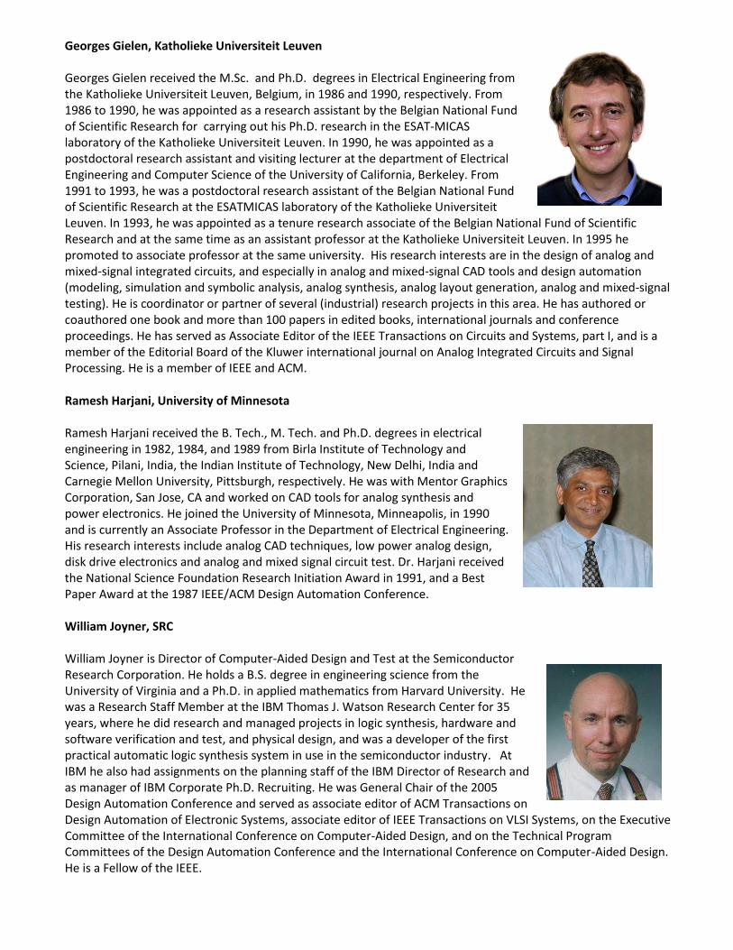
Georges Gielen, Katholieke Universiteit Leuven Georges Gielen received the M.Sc. and Ph.D. degrees in Electrical Engineering from the Katholieke Universiteit Leuven, Belgium, in 1986 and 1990, respectively. From 1986 to 1990, he was appointed as a research assistant by the Belgian National Fund of Scientific Research for carrying out his Ph.D. research in the ESAT-MICAS laboratory of the Katholieke Universiteit Leuven. In 1990, he was appointed as a postdoctoral research assistant and visiting lecturer at the department of Electrical Engineering and Computer Science of the University of California, Berkeley. From 1991 to 1993, he was a postdoctoral research assistant of the Belgian National Fund of Scientific Research at the ESATMICAS laboratory of the Katholieke Universiteit Leuven. In 1993, he was appointed as a tenure research associate of the Belgian National Fund of Scientific Research and at the same time as an assistant professor at the Katholieke Universiteit Leuven. In 1995 he promoted to associate professor at the same university. His research interests are in the design of analog and mixed-signal integrated circuits, and especially in analog and mixed-signal CAD tools and design automation (modeling, simulation and symbolic analysis, analog synthesis, analog layout generation, analog and mixed-signal testing). He is coordinator or partner of several (industrial) research projects in this area. He has authored or coauthored one book and more than 100 papers in edited books, international journals and conference proceedings. He has served as Associate Editor of the IEEE Transactions on Circuits and Systems, part I, and is a member of the Editorial Board of the Kluwer international journal on Analog Integrated Circuits and Signal Processing. He is a member of IEEE and ACM.
Ramesh Harjani, University of Minnesota Ramesh Harjani received the B. Tech., M. Tech. and Ph.D. degrees in electrical engineering in 1982, 1984, and 1989 from Birla Institute of Technology and Science, Pilani, India, the Indian Institute of Technology, New Delhi, India and Carnegie Mellon University, Pittsburgh, respectively. He was with Mentor Graphics Corporation, San Jose, CA and worked on CAD tools for analog synthesis and power electronics. He joined the University of Minnesota, Minneapolis, in 1990 and is currently an Associate Professor in the Department of Electrical Engineering. His research interests include analog CAD techniques, low power analog design, disk drive electronics and analog and mixed signal circuit test. Dr. Harjani received the National Science Foundation Research Initiation Award in 1991, and a Best Paper Award at the 1987 IEEE/ACM Design Automation Conference. William Joyner, SRC William Joyner is Director of Computer-Aided Design and Test at the Semiconductor Research Corporation. He holds a B.S. degree in engineering science from the University of Virginia and a Ph.D. in applied mathematics from Harvard University. He was a Research Staff Member at the IBM Thomas J. Watson Research Center for 35 years, where he did research and managed projects in logic synthesis, hardware and software verification and test, and physical design, and was a developer of the first practical automatic logic synthesis system in use in the semiconductor industry. At IBM he also had assignments on the planning staff of the IBM Director of Research and as manager of IBM Corporate Ph.D. Recruiting. He was General Chair of the 2005 Design Automation Conference and served as associate editor of ACM Transactions on Design Automation of Electronic Systems, associate editor of IEEE Transactions on VLSI Systems, on the Executive Committee of the International Conference on Computer-Aided Design, and on the Technical Program Committees of the Design Automation Conference and the International Conference on Computer-Aided Design. He is a Fellow of the IEEE.

Kevin Kemp, Freescale Dr. Kevin Kemp manages the strategic direction and execution of technology programs at Freescale Semiconductor, including research collaborations with universities to develop technologies for use in Freescale’s embedded semiconductor solutions. Dr. Kemp previously held research and engineering management positions at Motorola, FSI International, and Sematech, and contributed to the development and implementation of lithography processes and equipment at g-line through 193 nm and EUV wavelengths. Dr. Kemp has a Ph.D. in Electrical Engineering from Clemson University, and bachelors and masters degrees from the University of Natal in Durban, South Africa. Greg Loxtercamp, Medtronic Mr. Loxtercamp is a Principal IC Design Engineer at Medtronic.
Boris Murmann, Stanford University
Boris Murmann is an Associate Professor in the Department of Electrical Engineering, Stanford, CA. He received the Ph.D. degree in electrical engineering from the University of California at Berkeley in 2003. From 1994 to 1997, he was with Neutron Mikrolektronik GmbH, Hanau, Germany, where he developed low-power and smart-power ASICs in automotive CMOS technology. Dr. Murmann’s research interests are in the area of mixed-signal integrated circuit design, with special emphasis on data converters and sensor interfaces. In 2008, Dr. Murmann was a co-recipient of the Best Student Paper Award at the VLSI Circuit Symposium and the recipient of the Best Invited Paper Award at the Custom Integrated Circuits Conference (CICC). In 2009, he received the Agilent Early Career Professor Award. He currently serves as a member of the International Solid-State-Circuits Conference (ISSCC) program committee.
Kenneth O, University of Texas, Dallas Kenneth K. O is Professor of Electrical Engineering and Director of the SRC GRC Texas Analog Center of Excellence (TxACE) at the University of Texas/Dallas. He received the B.S., M.S., and Ph.D. degrees from MIT. Before joining UT Dallas in 2009, Dr. O was a professor of electrical and computer engineering at the University of Florida, where he taught and performed research for 15 years. Prior to that he worked at Analog Devices Inc. developing sub-micron CMOS processes for mixed signal applications and high-speed bipolar and BiCMOS processes for RF and mixed signal applications. He is perhaps best known among those in his field for helping make RF/CMOS the technology of choice for the billions of cell phone chips now in use. He has also helped expand the application of CMOS semiconductor technology by demonstrating its capability at ever-increasing frequencies. His University of Florida group holds the record for the highest operating frequency for transistor circuits. He is pursuing work funded by Texas Instruments, Semiconductor Research Corp., the U.S. Army Research Office and DARPA. He received an NSF Early Career Development Award in 1996, he has been a member of the International Advisory Committee for the Journal of Semiconductor Technology and Science since 2001, he has authored and co-authored 170 journal and conference publications, and he holds nine patents.

Sule Ozev, Arizona State University
Sule Ozev received her Ph.D. from University of California, San Diego's Computer Science and Engineering Department in 2002. That same year, she joined Duke University's Electrical and Computer Engineering Department as an assistant professor. She worked on testing mixed-signal and radiofrequency circuits, built-in-self test techniques, analysis and mitigation of process variations, defect-tolerant microprocessor systems, and online, and off-line testing of microfluidic devices. In August 2008, she joined Arizona State University's Electrical Engineering Department as an associate professor, continuing on the same line of research. She received NSF CAREER award in 2006, and various other awards from NSF, SRC, NASA, and IBM. She also received the best dissertation award from UCSD in 2002, the best paper award from IEEE International Conference on Computer Design in 2005, the TTTC Naveena Nagi Award at VTS in 2002, and the Best Session Award at VTS in 2006. She has published over 70 conference and journal papers and holds one US patent.
Sanjay Raman, DARPA
Sanjay Raman received his bachelor's degree in Electrical Engineering (with Highest Honor) from Georgia Tech in 1987. From 1987-1992 he served as a nuclear trained submarine officer with the U.S. Navy. During this time he was primarily responsible for the safe and efficient operation of a Sturgeon-class fast attack submarine and its S5W nuclear reactor. He was awarded the Navy Commendation Medal (1991) and Navy Achievement Medal (2 awards, 1990 and 1992), as well as various unit awards. Following his tour of duty with the Navy, he returned to graduate school at the University of Michigan and received a master's degree in Electrical Engineering in 1993. He completed his Ph.D. in Electrical Engineering at the University of Michigan in 1998 in the area of novel millimeter-wave integrated antennas and electronics. Janusz Rajski, Mentor Graphics Janusz Rajski is Chief Scientist and Director of Engineering at Mentor Graphics Corporation. He received the M.S. degree from the Technical University of Gdansk, Poland, in 1973, and the Ph.D. degree from the Technical University of Poznan, Poland, in 1982, both in electrical engineering. In 1984, he joined McGill University, Montreal, Canada, where he became an associate professor in 1989. In 1995, he accepted the position of chief scientist at Mentor Graphics Corporation. His main research interests include testing of VLSI systems, design for testability, built-in self-test, and logic synthesis. He has published over 100 technical papers and holds seventeen US and international patents in the area of design for test, and is the principal inventor of Embedded Deterministic Test technology. He is co-author of Arithmetic Built-In Self-Test for Embedded Systems published by Prentice Hall in 1997, and co-recipient of the 1993 Best Paper Award for the paper on synthesis of testable circuits published in the IEEE Trans. on CAD. He has served on technical program committees of various conferences including International Test Conference. Dr. Rajski is a co-founder of the International Test Synthesis Workshop.

Jaijeet Roychowdhury, University of California, Berkeley Jaijeet Roychowdhury is a Professor of EECS at the University of California, Berkeley. He received a Bachelor's degree in electrical engineering from the Indian Institute of Technology, Kanpur, India, in 1987, and a Ph.D. degree in electrical engineering and computer science from UC Berkeley in 1993. From 1993 to 1995, he was with the Computer-Aided Design (CAD) Laboratory, AT&T Bell Laboratories, Allentown, PA. From 1995 to 2000, he was with the Communication Sciences Research Division, Bell Laboratories, Murray Hill, NJ. From 2000 to 2001, he was with CeLight Inc. (an optical networking startup), Silver Spring, MD. From 2001-2008, he was with the Electrical and Computer Engineering Department and the Digital Technology Center at the University of Minnesota in Minneapolis. Roychowdhury's professional interests include the analysis, simulation and design of electronic, biological and mixed domain systems. He was cited for Extraordinary Achievement by Bell Laboratories in 1996. He has authored or co-authored seven best or distinguished papers at ASP-DAC, DAC, and ICCAD. He was an IEEE Circuits and Systems Society Distinguished Lecturer during 2003-2005 and served as Program Chair of IEEE's CANDE and BMAS workshops in 2005. He has served on the Technical Program Committees of ICCAD, DAC, DATE, ASP-DAC and other EDA conferences, on the Executive Committee of ICCAD, on the Nominations and Appointments Committee of CEDA, and as an Officer of CANDE. He is a Fellow of the IEEE.
Rob Rutenbar, University of Illinois at Urbana-Champaign
Rob A. Rutenbar received his Ph.D. from the University of Michigan in 1984, and then joined the faculty at Carnegie Mellon University. He joined the computer science faculty at the University of Illinois in January 2010, and is currently the Abel Bliss Professor of Engineering and head of the computer science department. He has worked on tools for custom circuit synthesis and optimization for over 20 years, and on custom silicon architectures for speech recognition for the last half dozen years. In 1998 he co-founded Neolinear Inc. to commercialize the first practical synthesis tools for analog designs. He served as Neolinear's Chief Scientist until its acquisition by Cadence in 2004. He is the founding Director of the US national Focus Research Center for Circuits and System Solutions. He has won many awards over his career, including the 2001 Semiconductor Research Corporation Aristotle Award for excellence in education, and most recently, the 2007 IEEE Circuits & Systems Industrial Pioneer Award. His work has been featured in venues ranging from "EE Times" to "The Economist" magazine. He is a Fellow of the IEEE.

Naresh Shanbhag, University of Illinois at Urbana-Champaign
Naresh R. Shanbhag received his Ph.D. degree in EE from the University of Minnesota in 1993. From July 1993 to August 1995, he worked in AT&T Bell Laboratories at Murray Hill, New Jersey, where he was responsible for the development of VLSI algorithms, architectures and implementation of broadband data communications transceivers. Since August 1995, he has been with the Department of Electrical and Computer Engineering, and the Coordinated Science Laboratory where he is presently a Professor. Dr. Shanbhag's research focuses on two major areas: the design of VLSI chips for broadband communications and the design of energy-efficient and reliable VLSI chips employing communication system design principles. He has published more than 90 journal articles/book chapters/conference publications in this area and holds three US patents. He is also a coauthor of the research monograph Pipelined Adaptive Digital Filters published by Kluwer Academic Publishers in 1994. Dr. Shanbhag received the 2006 IEEE Journal of Solid-State Circuits Best Paper Award, became a Fellow of IEEE in 2006, received the 2001 IEEE Transactions on VLSI Best Paper Award, the 1999 IEEE Leon K. Kirchmayer Best Paper Award, the 1999 Xerox Faculty Award, 2007 Distinguished Lecturership of IEEE Circuits and Systems Society, the National Science Foundation CAREER Award in 1996, and the 1994 Darlington Best Paper Award from the IEEE Circuits and Systems Society. From 1997-99 and from 1999-2002, he served as an Associate Editor for the IEEE Transaction on Circuits and Systems: Part II and the IEEE Transactions on VLSI, respectively. He has led the Alternative Computational Models research theme in the Gigascale Systems Research Center (GSRC) since 2006. Dr. Shanbhag is a co-founder and Chief Technology Officer of Intersymbol Communications, Inc., a venture-funded fabless semiconductor start-up acquired by Finisar Corporation in 2007, where Dr. Shanbhag serves as a Senior Scientist on a part-time basis.
Mani Soma, University of Washington
Mani Soma is currently the Associate Vice Provost for Research, Industry Relations and a professor of electrical engineering. At the Office of Research, Soma assists in building relationships with industry and with the development of online systems and tools for research administration. His research involves the design and test of integrated circuits and bioelectronic systems. Soma earned his bachelor's degrees in electrical engineering and math, with a minor in physics at California State University-Fresno. He then attended Stanford University for graduate studies, earning a doctorate in 1980. He worked for General Electric in Schenectady, NY, before coming to the University of Washington as an assistant professor in 1982. Prior to joining the Office of Research as an Associate Vice Provost for Research, he was the acting Dean of the College of Engineering, and was previously an assistant director and director of various centers, and an associate chairman and acting chairman for the Department of Electrical Engineering.
Greg Taylor, Intel
Greg Taylor is an Intel Fellow and director of the Circuit Research Lab in Intel Labs. He is responsible for research on low power and high speed circuits, high speed signaling, and enabling design and circuit technologies within Intel. Taylor joined Intel in 1991 and has held several senior design engineering positions working on 10 generations of microprocessors including members of Intel's Pentium®, Pentium® II, Pentium® III, and Intel NetBurst® microarchitecture families. Prior to joining Intel, he worked as a principal engineer at Bipolar Integrated Technology. Taylor is a Fellow of the Institute of Electrical and Electronics Engineers. He received his bachelor's degree in computer and systems engineering in 1981 from Rensselaer Polytechnic Institute (RPI). He also received a master's degree and doctorate in computer and systems engineering from RPI in 1983 and 1985, respectively. His graduate work was completed with the support of a Fellowship from the Fannie and John Hertz Foundation.

Friedrich Taenzler, Texas Instruments
Friedrich Taenzler is a Product/Test Engineering Manager for RF and mixed signal products within the HVAL organization in Texas Instruments. His main interests are the development of low cost test strategies and solutions as well as the required in-house ATE systems. The product mix he and his team are working on are in the field of commercial Si and GaAs devices up to 6GHz, automotive and medical mixed signal and RF devices as well MCU with new types of NVM devices. Friedrich Taenzler obtained his Dipl.-Ing and Doctorial degree in electrical engineering in 1988 and resp. 1994 from Mercator University Duisburg/Germany.
Robert Trew, NSF
Robert J. Trew received the Ph.D. degree from the University of Michigan in 1975. He is currently the Director of the Electrical, Communications, and Cyber Systems (ECCS) Division at NSF, and the Alton and Mildred Lancaster Distinguished Professor in the Electrical and Computer Engineering Department at North Carolina State University, Raleigh. Dr. Trew served as the ECE Department Head for eleven years at three different universities: NCSU, Virginia Tech, and Case Western Reserve University. From 1997 to 2001 Dr. Trew served as Director of Research in the Office of the Secretary of Defense, with management oversight responsibility for the basic research programs of DOD. During this time Dr. Trew directly managed DOD's University Research Initiative, which includes the MURI, DURIP, DEPSCoR, and HBCU/MI programs. He also represented the DOD basic research program to various organizations such as the White House Office of Science and Technology Policy (OSTP), the National Academies, professional societies, and other organizations devoted to national basic research policy. From 1997-98 he was DOD representative to the White House OSTP Committee on Science and the National Research Council's Government-University-Industry Research Roundtable (GUIRR). Dr. Trew served as Vice-Chair of the U.S. Government interagency committee that planned and implemented the U.S. National Nanotechnology Initiative (NNI). He also served as a Program Manager in the Electronics Division of the U.S. Army Research Office from 1992-97. Dr. Trew is a Fellow of the IEEE, and serves on the IEEE Microwave Theory and Techniques Society Administration Committee (ADCOM) and was MTT Society President for 2004. He is currently the Editor-in-Chief of the IEEE Proceedings. He was Editor-in-Chief of the IEEE Transactions on Microwave Theory and Techniques from 1995 to 1997, and from 1999-2002 was founding Co-Editor-in-Chief of IEEE Microwave Magazine. Dr. Trew performs research in the area of physically-based semiconductor device models for computer-aided design, nanoelectronics, wide bandgap semiconductor microwave devices, THz technology, and high frequency electronic devices. He was twice named an IEEE Microwave Distinguished Lecturer. Dr. Trew has received numerous awards, including the 2001 IEEE-USA Harry Diamond Memorial Award, an IEEE Third Millennium Medal Award, the 1998 IEEE MTT Society Distinguished Educator Award, the 1991 Alcoa Foundation Distinguished Engineering Research Award, and a 1992 NCSU Distinguished Scholarly Achievement Award. He received an Engineering Alumni Society Merit Award in Electrical Engineering from the University of Michigan in 2003. Dr. Trew has authored or co-authored over 170 publications, 20 book chapters, and has given over 390 technical and programmatic presentations. Dr. Trew has nine patents.

Andreas Weisshaar, NSF
Andreas Weisshaar received the Diplom-Ingenieur (Dipl.-Ing.) degree in electrical engineering from the University of Stuttgart (Germany) and the M.S. and Ph.D. degrees in electrical and computer engineering from Oregon State University. In 1991, he joined the faculty of the Department of Electrical and Computer Engineering (now School of Electrical Engineering and Computer Science) at Oregon State University, where he is Professor of Electrical Engineering and Computer Science. Since April 2008, he has been serving at the National Science Foundation as Program Director of the Communications, Circuits, and Sensing-Systems (formerly Integrative, Hybrid, and Complex Systems) Program in the Electrical, Communications and Cyber Systems (ECCS) Division. His current areas of research include CAD of passive RF and microwave circuits and components, embedded passives, interconnects and electronic packaging, and signal integrity. He has authored or co-authored numerous technical papers, authored several book chapters, and co-authored Transmission Lines and Wave Propagation, 4th Edition (Boca Raton, FL: CRC Press, 2001). He has served as Managing General Co-Chair of the 2009 IEEE Conference on Electrical Performance of Electronic Packaging and Systems and as its General Co-Chair in 2008. He served as Associate Editor of the IEEE Microwave and Wireless Components Letters (2003 - 2006) and as a Guest Editor of the IEEE Transactions on Microwave Theory and Techniques, December 2002 Symposium Issue. He is currently an Associate Editor of the IEEE Transactions on Advanced Packaging. Dr. Weisshaar is a Fellow of the IEEE.
David Yeh, SRC
David C. Yeh is currently a Texas Instruments resident at the Semiconductor Research Corporation, serving as Director of Integrated Circuits and Systems Sciences (ICSS) since 2005. In this position he funds and supports university research programs addressing high-speed, low-power, robustness, and manufacturability issues for digital, analog, mixed-signal, and RF integrated circuit designs. Dr. Yeh joined Texas Instruments in 1990 and held a Senior Member Technical Staff position in the High Performance Analog CAD group where he made significant contributions to the planning, development, support, and continual enhancement of TISpice3, an internal circuit simulation tool. In addition, from 2000 to 2004 he was TI’s representative to SRC’s Computer Aided Design and Test Science (CADTS) area, serving as that group’s Science Area Coordinating Committee Chairman in 2002 and 2003. In this role he helped develop digital, analog, RF, and mixed-signal CAD research needs for SRC member companies. He is a Senior Member of IEEE, and is a graduate of the University of Illinois at Urbana-Champaign (BS, MS, PhD).

National Science Foundation Workshop on Failure and Uncertainty in Mixed-Signal Circuits and Systems
Thursday, July 8, 2010
7:30 - 8:00 am Registration / Breakfast
8:00 - 8:15 am Welcome and Workshop Overview - Andreas Weisshaar / Robert Trew, NSF and David Yeh, SRC
Session I: Current Activities in Failure Resistant Systems (Chair: Saverio Fazzari, Booz Allen Hamilton)
8:15 - 8:35 am Sanjay Raman, DARPA Maximizing Performance Yield and Lifetime through In Situ Self-healing
8:35 - 8:55 am Kevin Kemp, Freescale Semiconductor, Inc.
System-Level Cross-Layer Cooperation to Achieve Predictable Systems from Unpredictable Components
8:55 - 9:15 am Georges Gielen, Katholieke Universiteit Leuven
Designing Reliable Analog/Mixed-Signal Circuits in Increasingly Unreliable CMOS Technologies
9:15 - 9:30 am Discussion
Session II: Mixed-Signal System Applications and Reliability Constraints (Chair: Marco Corsi, Texas Instruments)
9:30 - 9:50 am Ramesh Harjani, University of Minnesota Handling Reliability Concerns for Large Mixed-Signal Circuits
9:50 - 10:10 am Brian Floyd, North Carolina State University Trends and Challenges in Future RF Systems
10:10 - 10:30 am Mike Flynn, University of Michigan Mixed-Signal System Applications and Reliability Constraints
10:30 - 10:50 am Greg Loxtercamp - Medtronic Implantable Design Applications and Reliability Concerns
10:50 - 11:05 am Discussion
11:05 - 11:30 am Break
Session III: Reliable Mixed-Signal Devices and Circuits (Chair: Ken O, University of Texas/Dallas)
11:30 - 11:50 am Boris Murmann, Stanford University Calibration and Correction Issues in Nano-Scale Mixed-Signal Circuits
11:50 - 12:10 pm Ranjit Gharpurey, University of Texas/Austin Variability Related Challenges in RF and High-Frequency Analog Circuits
12:10 - 12:30 pm Terri Fiez, Oregon State University System-to-Circuit Design Considerations to Achieve 25 Year Reliability for Solar Applications
12:30 - 12:45 pm Discussion
12:45 - 1:45 pm Lunch
Session IV: Mixed-Signal Reliability Testing and Validation (Chair: Friedrich Taenzler, Texas Instruments)
1:45 - 2:05 pm Mani Soma, University of Washington
Missing in Action: Critical Gaps in Reliability Test and Validation Methods for Mixed-Signal Blocks and Systems
2:05 - 2:25 pm Abhijit Chatterjee, Georgia Tech University Adaptive Mixed-Signal/RF Processing
2:25 - 2:45 pm Sule Ozev, Arizona State University
Vertically-Integrated Test/Calibration and Reliability Enhancement for Systems with RF/Analog Content
2:45 - 3:00 pm Discussion

Session V: Reliability at Different Levels of Design Abstraction (Chair: Sudhir Gowda, IBM Corporation)
3:00 - 3:20 pm Andreas Cangellaris, University of Illinois/Urbana-Champaign
EM-CAD Needs and Challenges for Robust Mixed-Signal IC and System Design
3:20 - 3:40 pm Naresh Shanbhag, University of Illinois/Urbana-Champaign
Mixed-Signal Reliability Challenges: A Communication-Inspired View
3:40 - 4:00 pm Greg Taylor, Intel Corporation Design for Resilience
4:00 - 4:15 pm Discussion
4:15 - 4:45 pm Break
Session VI: Design Flow and Tools for Mixed-Signal Reliability (Chair: Janusz Rajski, Mentor Graphics Corporation)
4:45 - 5:05 pm Luca Daniel, Massachusetts Institute of Technology
Needs & Challenges in Uncertainty Simulation/Modeling Tools for Mixed-Signal Circuits and Systems
5:05 - 5:25 pm Jaijeet Roychowdhury, University of California/Berkeley University Research in Mixed-Signal CAD
5:25 - 5:45 pm Rob Rutenbar, University of Illinois/Urbana-Champaign Analog Reliability Via Analog Synthesis
5:45 - 6:00 pm Discussion
6:00 - 6:30 pm Key Points by Session Chairs - 5 minutes each
7:00 pm Working Dinner Willow Restaurant, 4301 N. Fairfax Drive, Arlington, VA
Friday, July 9, 2010
7:30 - 8:00 am Breakfast
8:00 - 8:30 am Changes to Key Points
Breakout 1 Breakout 2
8:30 - 9:00 am Session 1 Discussion Session 4 Discussion
9:00 - 9:30 am Session 2 Discussion Session 5 Discussion
9:30 - 10:00 am Session 3 Discussion Session 6 Discussion
10:00 - 10:30 am Break
10:30 - 12:00 pm Discussion and Next Steps
12:00 - 1:00 pm Lunch
1:00 pm Adjourn