first monolithically integrated dual phase sensitive ... · quantum electronics, ... saturated...
TRANSCRIPT

Quantum Electronics, IEEE Journal of 1
Abstract—For the first time, a monolithically integrated
photonic phase-sensitive amplification chip is fabricated and
demonstrated based on an InP/InGaAsP platform. Different
semiconductor optical amplifiers have been fabricated as well for
characterization. On the chip, two tunable laser pumps that are
coherently injection-locked, respectively, from two first-order
sidebands of an externally modulated tone are generated to enable
signal-degenerate dual-pumped phase-sensitive amplification in a
saturated semiconductor optical amplifier. Experiments on
different chips are conducted to successfully demonstrate
phase-sensitive amplification with approximately 6.3 dB and 7.8
dB extinction of phase-sensitive on-chip gain. Theoretical
simulations are performed and agree well with experimental
results. The additive noise properties of the phase-sensitive
amplification chip are also investigated.
Index Terms—Phase sensitive amplifier, semiconductor optical
amplifier, photonic integrated circuit, four-wave mixing
I. INTRODUCTION
PTICALphase-sensitive amplifiers (PSAs) have been
attracting increasing attention [1,2]due to unique
advantages that enable them to break the 3-dB quantum
limit of the noise figure (NF)[3], as well as achieve the phase
regeneration to reduce phase and time jitters in optical
transmission links [4-6]. Unlike a conventional
phase-insensitive amplifier (PIA) such as an erbium-doped
Manuscript received September 28, 2015; revised XX00, 2015; accepted
XX00, 2015. This work was supported by DARPA DSO. Wangzhe Li, Shamsul Arafin, Danilo Dadic, Leif A. Johansson and Larry A.
Coldren are with the Department of Electrical and Computer Engineering,
University of California, Santa Barbara, CA, 93110 (e-mail: [email protected]).
Mingzhi Lu was with University of California, Santa Barbara; Santa
Barbara; CA 93110 USA. He is now with Infinera Corporation, 140 Caspian Ct., Sunnyvale, CA 94089 USA. (email: [email protected])
Antonio Mecozzi is now with the Department of Physical and Chemical
Sciences, University of L’Aquila, L’Aquila 67100, Italy. (e-mail: [email protected]).
Michael Vasilyev is with the Department of Electrical Engineering,
University of Texas at Arlington, Arlington, TX 76019-0016 USA. (e-mail: [email protected]).
fiber amplifier (EDFA), featuring an inherent minimum NF of
3-dB [7], a PSA is capable of amplifying only one of the two
quadrature phase components in a light wave signal and
attenuating the other. This unique feature makes it possible in
theory to realize noise free amplification, leading to a NF of 0
dB, which can find numerous applications where noise levels
are critical, such as optical telecommunication, remote sensing,
optical spectroscopy, LIDAR and inter-satellite communication.
Various PSAs have been demonstrated by using parametric
down-conversion in χ(2)
-based nonlinear materials[8, 9], such
as periodically poled LiNbO3 (PPLN) waveguides and
nonlinear optical loop mirrors (NOLMs) [10], or using
four-wave mixing (FWM) in χ(3)
-based nonlinear media like
optical fibers [2] and unsaturated semiconductor optical
amplifiers (SOAs) [11]. New CMOS-compatible platforms are
also emerging [12].
Among all demonstrated PSAs so far, their implementations
are based on free-space bulk-crystal system or bench-top fiber
systems, which makes it difficult to use them in practical
scenarios. One of the challenges in realizing a practical PSA is
that at input port of the PSA the phase relationship between the
pump(s) and the signal must be synchronized and stabilized.
Some solutions to synchronization of the pump and signal
phases have been developed via pump injection locking [13]
and optical phase-locked loop [14], which usually increase the
complexity of the system and make it more unsuitable for use in
a real application. In addition, other issues in terms of size,
weight, power consumption and coupling losses also restrict the
bench-top PSA’s commercial allure. In order to solve this issue,
photonic integration is a promising solution and can great
benefit the implementation of PSAs for practical applications.
Other than some obvious advantages like small footprint, light
weight, reduced coupling losses and batch fabrication
economies, integrated photonic chips can inherently guarantee
a stable phase relationship among signal and pumps, requiring
no phase-locking mechanisms, which significantly eases the
implementation and practical application of PSAs.
In this paper, based on the implementation of a PSA through
a dual-pump degenerate FWM process, a chip-scale PSA using
a saturated SOA as a nonlinear element and different SOAs for
First Monolithically Integrated Dual-Pumped
Phase-Sensitive Amplifier Chip Based on a
Saturated Semiconductor Optical Amplifier
Wangzhe Li,Member, IEEE, Mingzhi Lu, Antonio Mecozzi,Fellow, IEEE, Michael Vasilyev,Senior
Member,IEEE, Shamsul Arafin, Member, IEEE, Danilo Dadic,Leif A. Johansson,Member, IEEE, and
Larry A. Coldren, Fellow, IEEE
(Invited Paper)
O
Quantum Electronics, IEEE Journal of 2
characterization have been fabricated and for the first time an
integrated photonic PSA chip has been experimentally
demonstrated. The chip and SOAs fabrication is based on an
InP/InGaAsP centered quantum well (CQW) platform. On the
chip, two tunable laser pumps that are coherently
injection-locked from sidebands of an external modulated light
wave are obtained to realize signal-degenerate dual-pumped
PSA in a highly saturated SOA. A 6.3 dB and a 7.8 dB
extinction ratio of gain based on different PSA chips are
realized, which both agree well with simulation results. The
reduction in signal-to noise ratio is also estimated based on the
measured optical spectrum of the light waves before and after
the PSA.
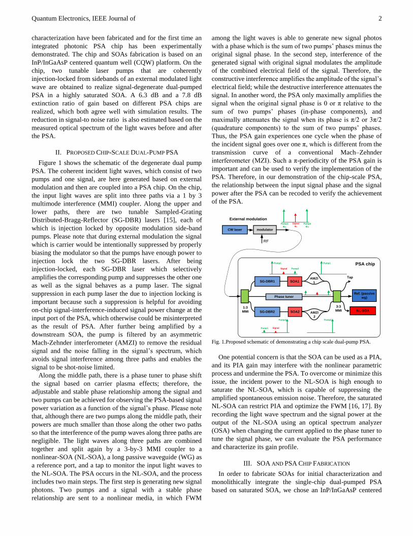
II. PROPOSED CHIP-SCALE DUAL-PUMP PSA
Figure 1 shows the schematic of the degenerate dual pump
PSA. The coherent incident light waves, which consist of two
pumps and one signal, are here generated based on external
modulation and then are coupled into a PSA chip. On the chip,
the input light waves are split into three paths via a 1 by 3
multimode interference (MMI) coupler. Along the upper and
lower paths, there are two tunable Sampled-Grating
Distributed-Bragg-Reflector (SG-DBR) lasers [15], each of
which is injection locked by opposite modulation side-band
pumps. Please note that during external modulation the signal
which is carrier would be intentionally suppressed by properly
biasing the modulator so that the pumps have enough power to
injection lock the two SG-DBR lasers. After being
injection-locked, each SG-DBR laser which selectively
amplifies the corresponding pump and suppresses the other one
as well as the signal behaves as a pump laser. The signal
suppression in each pump laser the due to injection locking is
important because such a suppression is helpful for avoiding
on-chip signal-interference-induced signal power change at the
input port of the PSA, which otherwise could be misinterpreted
as the result of PSA. After further being amplified by a
downstream SOA, the pump is filtered by an asymmetric
Mach-Zehnder interferometer (AMZI) to remove the residual
signal and the noise falling in the signal’s spectrum, which
avoids signal interference among three paths and enables the
signal to be shot-noise limited.
Along the middle path, there is a phase tuner to phase shift
the signal based on carrier plasma effects; therefore, the
adjustable and stable phase relationship among the signal and
two pumps can be achieved for observing the PSA-based signal
power variation as a function of the signal’s phase. Please note
that, although there are two pumps along the middle path, their
powers are much smaller than those along the other two paths
so that the interference of the pump waves along three paths are
negligible. The light waves along three paths are combined
together and split again by a 3-by-3 MMI coupler to a
nonlinear-SOA (NL-SOA), a long passive waveguide (WG) as
a reference port, and a tap to monitor the input light waves to
the NL-SOA. The PSA occurs in the NL-SOA, and the process
includes two main steps. The first step is generating new signal
photons. Two pumps and a signal with a stable phase
relationship are sent to a nonlinear media, in which FWM
among the light waves is able to generate new signal photos
with a phase which is the sum of two pumps’ phases minus the
original signal phase. In the second step, interference of the
generated signal with original signal modulates the amplitude
of the combined electrical field of the signal. Therefore, the
constructive interference amplifies the amplitude of the signal’s
electrical field; while the destructive interference attenuates the
signal. In another word, the PSA only maximally amplifies the
signal when the original signal phase is 0 or π relative to the
sum of two pumps’ phases (in-phase components), and
maximally attenuates the signal when its phase is π/2 or 3π/2
(quadrature components) to the sum of two pumps’ phases.
Thus, the PSA gain experiences one cycle when the phase of
the incident signal goes over one π, which is different from the
transmission curve of a conventional Mach–Zehnder
interferometer (MZI). Such a π-periodicity of the PSA gain is
important and can be used to verify the implementation of the
PSA. Therefore, in our demonstration of the chip-scale PSA,
the relationship between the input signal phase and the signal
power after the PSA can be recoded to verify the achievement
of the PSA.
CW laser modulator
External modulation
RF
Signal
φS
Pump1
φP1
Pump2
φP2
AMZI
1SOA1
SOA2 AMZI
2
SG-DBR1
SG-DBR2
1:3
MMI
3:3
MMI NL-SOA
Ref. (passive
wg)
Tap
Phase tuner
SignalPump1
Pump2 Pump2
Pump1
Signal
Pump1
Pump2
PSA chip
Fig. 1.Proposed schematic of demonstrating a chip scale dual-pump PSA.
One potential concern is that the SOA can be used as a PIA,
and its PIA gain may interfere with the nonlinear parametric
process and undermine the PSA. To overcome or minimize this
issue, the incident power to the NL-SOA is high enough to
saturate the NL-SOA, which is capable of suppressing the
amplified spontaneous emission noise. Therefore, the saturated
NL-SOA can restrict PIA and optimize the FWM [16, 17]. By
recording the light wave spectrum and the signal power at the
output of the NL-SOA using an optical spectrum analyzer
(OSA) when changing the current applied to the phase tuner to
tune the signal phase, we can evaluate the PSA performance
and characterize its gain profile.
III. SOA AND PSA CHIP FABRICATION
In order to fabricate SOAs for initial characterization and
monolithically integrate the single-chip dual-pumped PSA
based on saturated SOA, we chose an InP/InGaAsP centered

Quantum Electronics, IEEE Journal of 3
quantum well (CQW) platform with 10 quantum wells (QWs)
[18] because such a platform is capable of maximizing the
mode overlap with the QWs in an SOA, enhancing the
nonlinearity and maximizing the FWM.
The fabrication started with a base epi, which includes
quantum well layers, waveguide layers and N-cladding layer.
Active and passive areas were defined using quantum
well-intermixing (QWI) technology [19]. The passive
waveguide with intermixed quantum wells still confine carriers
well, which is ideal for low-loss phase tuners. Then, by using
electron beam lithography and methane/hydrogen/argon
(MHA)-based RIE etching, the gratings of the SG-DBR laser
were defined. Following the grating definition, a blanket
p-cladding and p-contact layer regrowth was carried out using
metalorganic chemical vapor deposition (MOCVD). After the
regrowth, waveguides were defined and etched. In order to
have better heat dissipation and compactness at the same time,
surface ridge waveguides were used for the straight SG-DBR
lasers, while more-narrow deeply-etched waveguides were
used for other components on the chip, which leads to better
flexibility for waveguide routing and better SOA nonlinear
efficiency due to a higher confinement factor. Cl2/H2/Ar
ICP-RIE dry etching as well as InP wet etching was used to
defined the features. Following the waveguide etching,
P-contact vias were opened and Pt/Ti/Pt/Au was deposited as
the P contact metal. To further decrease the passive waveguide
loss and provide electrical isolation, we implanted protons in
the p-cladding layer of the passive waveguides. The wafer was
then thinned down to about 130 μm for ease of cleaving.
Backside Ti/Pt/Au metallization provided common cathode
connections to the n-type substrate. After cleaving and
anti-reflection coating of the waveguide facets, the discrete
SOAs and the PSA chips were ready for characterization. The
SOAs and the chip-scale PSA were fabricated on the same
wafer so that the specifications of the SOAs would be identical
to those of the SOAs in the PSA chip. The length and width of
the PSA chip are about 1 mm and 7 mm.
(a)
(b)
Fig. 2.(a)Schematic diagram of the PSA chip; (b)mask layout of the PSA-chip for fabrication
IV. SOA CHARACTERIZATION
Figure 3 shows all the different SOAs we fabricated. The
longest SOAs are used to evaluate the dispersion. The
high-speed SOAs which are the shortest are used to measure
SOA’s carrier lifetime; while the 1-mm SOAs are used to
characterize their gain profile.
2.3-mm SOAs 1-mm SOAsHigh-speed SOAs
Fig. 3.Photo of the fabricated SOAs with different lengths. (left) 2.3-mm SOAs consisting of three cascaded SOAs with a length of 766 µm; (middle)
high-speed SOAs with a length of 50, 100 and 150 µm; (right) 1-mm SOAs
consisting of three identical SOAs with a length of 333µm.
A. Carrier Lifetime Measurement
High-speed short SOAs were used to measure the carrier
lifetime. The setup is shown in Fig. 4, which mainly includes an
external cavity laser (ECL), an erbium-doped fiber amplifier
(EDFA), a variable optical attenuator (VOA), a bandpass filter
(BPF), a high-speed SOA, a photodetector (PD) and an
electrical spectrum analyzer (ESA). A wavelength from the
ECL was sent to the SOA through the EDFA, the VOA and the
BPF which were used to control the input light wave power. To
measure the SOA’s carrier lifetime, we first measured its
frequency response. To do so, an RF signal and a bias voltage
were applied to the SOA via a bias-tee to modulate the light
wave that was passing through the SOA. The SOA’s output was
converted by the PD to re-generate the RF frequency which was
recorded and measured by the ESA.
Fig. 4. SOA lifetime measurement setup
The length of the SOA under test is 50 µm, biased with a
current density of 6.67 kA/cm2. We measured SOA’s frequency
response given different input power, and then based on its
3-dB bandwidth, the lifetime could be calculated. We plotted
the relationship between the carrier lifetime and the input
power to the SOA, as shown in Fig. 5. As it can be seen, the
carrier lifetime goes down to 180 µm as the input power
increases to about 21 mW.
Input power (mW)
Ca
rrie
r lif
etim
e (
ps)
Fig. 5.Measured SOA carrier lifetime given different incident light wave power.
Quantum Electronics, IEEE Journal of 4
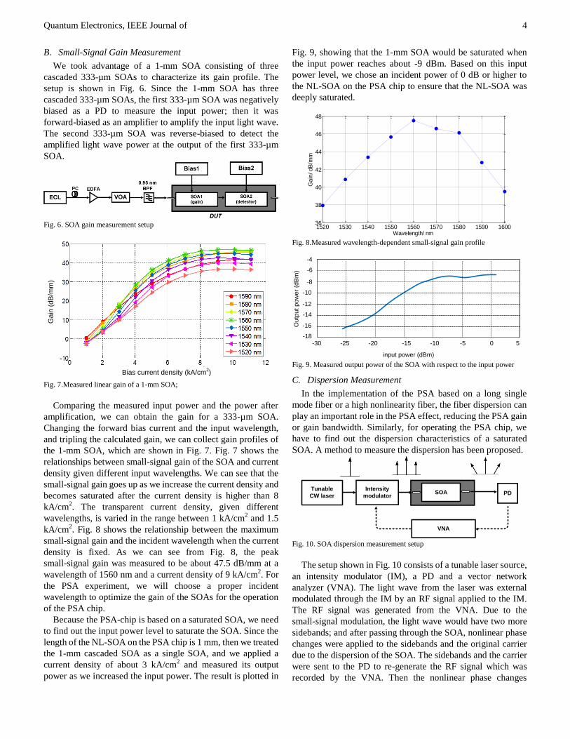
B. Small-Signal Gain Measurement
We took advantage of a 1-mm SOA consisting of three
cascaded 333-µm SOAs to characterize its gain profile. The
setup is shown in Fig. 6. Since the 1-mm SOA has three
cascaded 333-µm SOAs, the first 333-µm SOA was negatively
biased as a PD to measure the input power; then it was
forward-biased as an amplifier to amplify the input light wave.
The second 333-µm SOA was reverse-biased to detect the
amplified light wave power at the output of the first 333-µm
SOA.
Fig. 6. SOA gain measurement setup
Bias current density (kA/cm2)
Ga
in (
dB
/mm
)
Fig. 7.Measured linear gain of a 1-mm SOA;
Comparing the measured input power and the power after
amplification, we can obtain the gain for a 333-µm SOA.
Changing the forward bias current and the input wavelength,
and tripling the calculated gain, we can collect gain profiles of
the 1-mm SOA, which are shown in Fig. 7. Fig. 7 shows the
relationships between small-signal gain of the SOA and current
density given different input wavelengths. We can see that the
small-signal gain goes up as we increase the current density and
becomes saturated after the current density is higher than 8
kA/cm2. The transparent current density, given different
wavelengths, is varied in the range between 1 kA/cm2 and 1.5
kA/cm2. Fig. 8 shows the relationship between the maximum
small-signal gain and the incident wavelength when the current
density is fixed. As we can see from Fig. 8, the peak
small-signal gain was measured to be about 47.5 dB/mm at a
wavelength of 1560 nm and a current density of 9 kA/cm2. For
the PSA experiment, we will choose a proper incident
wavelength to optimize the gain of the SOAs for the operation
of the PSA chip.
Because the PSA-chip is based on a saturated SOA, we need
to find out the input power level to saturate the SOA. Since the
length of the NL-SOA on the PSA chip is 1 mm, then we treated
the 1-mm cascaded SOA as a single SOA, and we applied a
current density of about 3 kA/cm2 and measured its output
power as we increased the input power. The result is plotted in
Fig. 9, showing that the 1-mm SOA would be saturated when
the input power reaches about -9 dBm. Based on this input
power level, we chose an incident power of 0 dB or higher to
the NL-SOA on the PSA chip to ensure that the NL-SOA was
deeply saturated.
Fig. 8.Measured wavelength-dependent small-signal gain profile
-30 -25 -20 -15 -10 -5 0 5
Ou
tpu
t p
ow
er
(dB
m)
-4
-6
-8
-10
-12
-14
-16
-18
input power (dBm) Fig. 9. Measured output power of the SOA with respect to the input power
C. Dispersion Measurement
In the implementation of the PSA based on a long single
mode fiber or a high nonlinearity fiber, the fiber dispersion can
play an important role in the PSA effect, reducing the PSA gain
or gain bandwidth. Similarly, for operating the PSA chip, we
have to find out the dispersion characteristics of a saturated
SOA. A method to measure the dispersion has been proposed.
PDTunable
CW laser
Intensity
modulatorSOA
VNA
Fig. 10. SOA dispersion measurement setup
The setup shown in Fig. 10 consists of a tunable laser source,
an intensity modulator (IM), a PD and a vector network
analyzer (VNA). The light wave from the laser was external
modulated through the IM by an RF signal applied to the IM.
The RF signal was generated from the VNA. Due to the
small-signal modulation, the light wave would have two more
sidebands; and after passing through the SOA, nonlinear phase
changes were applied to the sidebands and the original carrier
due to the dispersion of the SOA. The sidebands and the carrier
were sent to the PD to re-generate the RF signal which was
recorded by the VNA. Then the nonlinear phase changes
1520 1530 1540 1550 1560 1570 1580 1590 160036
38
40
42
44
46
48
Wavelength/ nm
Gain
/ dB
/mm
SOA wavelength dependent gain
Quantum Electronics, IEEE Journal of 5
introduced by the dispersion could be recovered by the
comparing the RF phase changes. When we swept the input
wavelength and recorded the corresponding nonlinear phase
changes or the RF phase differences, we could calculate the
dispersion of the SOA.
Dis
pe
rsio
n
(ps/n
m-k
m)
1450 1500 1550 1600
Wavelength(nm)
20
15
10
5
0
Measured
Standard
Fig. 11.Comparison of the measured dispersion of a 2-meter SMF and its
standard dispersion value.
Before measuring the dispersion of the SOA, we need to
evaluate this setup and prove it is functional. Therefore, we use
the setup to measure the dispersion of a 2-meter signal mode
fiber (SMF) and compared the result with the standard
dispersion result of an ITU G.653 single mode fiber. The input
wavelength was shifted from 1545 nm to 1575 nm. As we can
see from Fig. 11, at 1550 nm, the measured result agrees well
with the standard dispersion value; The dispersion slot is
different, which could be caused by the facts that the standard
SMF dispersion is based on a few km meter fiber (averaging
thousands of different 2-meter SMFs) and the input wavelength
was not stable and drifting during the experiment.
Fig. 12 Measured SOA dispersion curves given different temperatures and
input powers.
After proving that the setup in Fig. 10 is functional, we
measured the dispersion of a 2.3-mm SOA given different
temperature and input power. The input power was set to be 0
dBm and 10 dBm, which are high enough to saturate the SOA.
Please note that before each measurement, we removed the
SOA first and measured the background dispersion including
the modulator and the 16-meter fiber in the setup.
The measured dispersion is shown in Fig. 12, as we can see,
dispersion curves are not flat. When temperature was fixed at 0
degree Celsius, given a 0-dBm input power, the dispersion is
flat and close to 0 fs/nm when the wavelength falls in a range
between 1550 nm to 1570 nm. At a shorter wavelength range
between 1525 nm to 1545 nm, there is a dispersion notch, and
the saturated SOA shows a relatively large dispersion of -700
fs/nm, or -304 fs/nm/mm at a wavelength of 1530 nm. When
the input power was increased to 10 dBm to further saturate the
SOA, the measurement can only covers a wavelength range
from 1545 nm to 1575 nm because of the limited gain
bandwidth of the EDFA we used in the experiment; however,
thanks to the appearance of the right edge of the notch, we can
still tell that the dispersion curves are red-shifted. Then we
increased the temperature to 35 degree Celsius, we repeated the
measurement and found out that the dispersion characteristics
stayed the same.
The measurement still has a few issues. The wavelength
instability caused dispersion ripples on the curves; large
background dispersion introduced by the 16-meter long fiber in
the setup made it difficult to accurately measure the small
amount of dispersion.
For the future PSA experiment and simulation, we chose the
incident wavelength around 1560 nm and treated the SOA as
dispersion-free element.
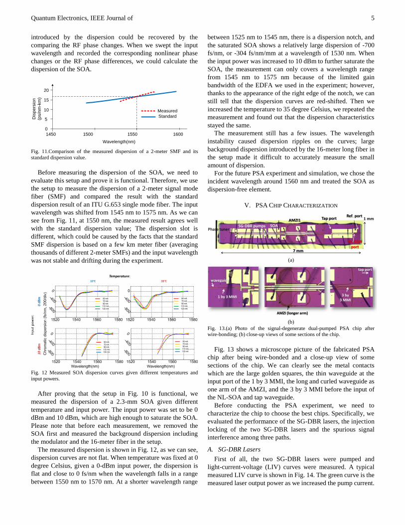
V. PSA CHIP CHARACTERIZATION
(a)
(b)
Fig. 13.(a) Photo of the signal-degenerate dual-pumped PSA chip after wire-bonding; (b) close-up views of some sections of the chip.
Fig. 13 shows a microscope picture of the fabricated PSA
chip after being wire-bonded and a close-up view of some
sections of the chip. We can clearly see the metal contacts
which are the large golden squares, the thin waveguide at the
input port of the 1 by 3 MMI, the long and curled waveguide as
one arm of the AMZI, and the 3 by 3 MMI before the input of
the NL-SOA and tap waveguide.
Before conducting the PSA experiment, we need to
characterize the chip to choose the best chips. Specifically, we
evaluated the performance of the SG-DBR lasers, the injection
locking of the two SG-DBR lasers and the spurious signal
interference among three paths.
A. SG-DBR Lasers
First of all, the two SG-DBR lasers were pumped and
light-current-voltage (LIV) curves were measured. A typical
measured LIV curve is shown in Fig. 14. The green curve is the
measured laser output power as we increased the pump current.

Quantum Electronics, IEEE Journal of 6
The kink on the curve represents a mode-hopping which was
caused by the internal temperate and refractive index change as
we changed the current. As we can see, the SG-DBR laser has a
threshold of about 30 mA at a temperature of 20 degree Celsius,
and a maximum output power of about 18 dBm at a bias current
of 120 mA. However, when both SG-DBR lasers were turned
on, the maximum output of each one was only about 12 dBm or
less due to heating effect.
Current (mA)
Mode
hopping
Fig. 14.Measured LIV curve of a SG-DBR laser.
1561.35
Wavelength (nm)
Sig
na
l p
ow
er
(dB
m)
-80
-70
-60
-50
-40
-30
-20
-10
0
1562.351561.85
0.1 nm/div = 12.5 GHz/div
Fig. 15.Measured optical spectrum of the output of two free-running SG-DBR
lasers.
The outputs of two SG-DBR lasers were measured as well
using an optical spectrum analyzer (OSA, with a resolution of
0.01 nm) and shown in Fig. 15. The two wavelengths are
spacing around 0.15 nm, which is equivalently 18.7 GHz. We
can easily tune the wavelengths by changing the current applied
to the corresponding phase section in each SG-DBG laser. The
averaged tuning rate is about 1.18 GHz/mA. However, due to
heating effect, tuning one wavelength always changed the other
one in the experiment.
B. Injection Locking of Two SG-DBR Lasers
Because injection locking two SG-DBR lasers is important
to make sure that the two pumps and the signal sent to the
NL-SOA to have the stable phase relationship, we have to
evaluate the injection locking performance of each laser.
We simply used an external laser to send the light wave to the
chip and turned on only one SG-DBR laser. Then at the tap
port, we used an OSA to monitor two wavelengths and started
to align them with each other. Once they were close enough, we
coupled the output of the tap to an external PD to convert the
light waves to an electrical beat note which was analyzed by an
ESA and we observed an unstable peak due to the random
phase relationship between two wavelengths. When the spacing
between two wavelengths became closer and closer, we
observed that the central frequency of the beat decreased. Once
the two wavelengths were close enough, the beat signal
disappeared and only a flat noise floor appeared on the ESA
which indicated that the SG-DBR laser was injection locked
and its wavelength was as same as the external one. By shifting
the wavelength of the sideband through changing the frequency
of the modulation RF signal, and the incident sideband power,
we measured the injection locking range with respect to
different injection ratio. The injection ratio is the power ratio of
the incident sideband power to the laser output. Then we turned
off the laser, turned on the other and repeated the same
measurement. The results are plotted in Fig. 16. As we can see
that the maximum locking ranges are about 4.5 GHz and 3.8
GHz when the injection ratio is maximized in the experiment.
However, for the PSA experiment, both SG-DBR lasers must
be injection-locked, the total input power from external
modulation was distributed on two sidebands (the signal power
can be ignored), which reduced the injection ratio by 3 dB.
Therefore, only 3 GHz and 2.2 GHz injection locking ranges
can be achieved. Considering the laser wavelength shifting due
to cross heating effect when we changed the phase tuner
current, the real locking range for each laser would be smaller.
-40 -30 -20 -10 0
Lo
ck
ing
ra
ng
e (
GH
z)
Injection ratio (dB)
0
5
4
3
2
1
Fig. 16.Measured injection locking ranges of two SG-DBR lasers given
different injection ratios.
Δν < 1kHz
Frequency (GHz, 10kHz/div)
Fig. 17.Measured electrical spectrum of the beat by heterodyning the
wavelengths from two injection-locked SG-DBR lasers.

Quantum Electronics, IEEE Journal of 7
Once two SG-DBR lasers were both injection- locked by the
two pumps from external modulation, the beat note of two
wavelengths at a PD becomes a very stable and narrow line and
can be monitored by the ESA, as shown in Fig. 17. The
resolution bandwidth of the ESA was about 100 Hz. The 3-dB
bandwidth of the beat is less than 1 kHz, which means that once
two SG-DBR lasers are injection locked, their relative
frequency spacing is fixed and determined by the two pumps
and their relative linewidth is also less than 1 kHz. Thus, once
we obverse a stable peak with a frequency of twice the RF
modulation frequency at the ESA, we can claim that the two
SG-DBR lasers are injection-locked. During the PSA
experiment we conducted, we always used the ESA to monitor
the beat note of two SG-DBR lasers through the tap port to
make ensure the injection locking was enabled.
C. Spurious Signal Interference
As we mentioned before, another advantage of injection
locking is the suppression of the signal, which ensures that
signal passes through the upper and middle paths, causing
signal interference and leading to possible misinterpreted PSA
effect. Therefore, after two SG-DBR lasers were
injection-locked and before we started to evaluate the PSA by
recording the signal power at the output of the NL-SOA, we
have to first rule out the possibility of the signal interference
among three paths to avoid improper interpretation of the PSA
when shifting the signal phase by change the phase tuner
current. Thus, at the output of the tap port, the signal power
with respect to time and phase tuner current were measured and
compared, as shown in Fig. 18. The blue solid curve is the
measured signal power as we increased phase tuner current;
while the dotted red curve is the measured signal power over
time. By comparing two curves here, only similar random
power fluctuations of about ± 0.5 dB were observed in two
cases and no obvious interference among three paths was
observed.
In addition, the power of the SG-DBR pump waves along the
upper and the lower paths were about 15 dB higher than those
along the middle path, therefore, the pump interference which
could cause PSA gain drift can be ignored as well, and the
signal power change at the output of the NL-SOA would be
only caused by the PSA.
-39
-37
Phase tuner current (mA)
Sig
na
l p
ow
er
(dB
m)
Time (s)
0 5 10 15 20 25 30 35 40
0 0.5 1 1.5 2 2.5 3 3.5 4
-41 Signal power vs time, current = 0 mA
Signal power vs phase tuner current
-35
-36
-38
-40
-42
Fig. 18.Measured signal power at the output of the tap with and without phase
tuner current changing.
D. Phase Tuner Characterization and Phase Shift
Measurement
Tuning the phase of the signal is important for the PSA
experiment. And knowing the exact phase shift when we tune
the current applied to the phase tuner is more important because
we need to take advantage of π-periodicity of the PSA gain
curve to verify the PSA. To obtain relative phase change of the
signal, we used the setup shown in Fig. 19.
AMZI
1SOA1
SOA2 AMZI
2
SG-DBR1
SG-DBR2
1:3
MMI
3:3
MMI NL-SOA
Ref. (passive wg)
Tap
Phase tunerCW laserIntensity
modulator
RF
SignalPump1 Pump2
PSA chip
External
modulation
Pump1
VNA PDSignalPump1 Pump2
Fig. 19.Relative signal phase measurement setup.
The RF signal for the external modulation was from the
VNA. One SG-DBR laser was turned off so that only one
SG-DBR laser was injection locked and only one sideband was
selectively amplified. Please note that the power of the
amplified sideband was much larger than those of sidebands
along the middle path so that the later were ignored. The signal
and the amplified sideband at the output of the tap were sent to
the PD to re-generate the RF signal whose phase change would
be identical to that of the optical signal. Therefore, by using the
VNA to measure the phase change of the received the RF signal
when changing the phase tuner current, we were able to
equivalently get the relative phase change of the optical signal.
The result is shown in Fig. 20. The abscissa variable is set to be
the square root of the phase tuner current because the signal
phase in theory varies linearly with the square root of the phase
tuner current. As we can see, there was no obvious phase
change of the signal until after the current was larger than 1
mA. Such a delay in phase shift commonly occurs in tunable
SG-DBR lasers and could be caused by an N+ sheet charge that
exists at the regrowth interface due to surface contamination.
As the current was further increased, these traps are filled and
phase shift appeared. Overall, 1 mA0.5
gives π phase shift of the
signal.
0 0.2 0.4 0.6 0.8 1 1.2 1.4 1.6 1.8 2
Square root of current (mA0.5
)
Re
lative
sig
na
l p
ha
se
(π
·ra
d)
-1.6
-1.2
-0.8
-0.4
0
0.4
0.8
-2.0
1 mA0.5
gives π phase shift
Fig. 20.Measured relative signal phase change.
To help evaluate the signal phase measurement, we also
formed an on-chip MZI by deactivating the lower path. Without

Quantum Electronics, IEEE Journal of 8
external modulation, we sent one wavelength to the chip and
injection locking one SG-DBR laser and measured the output
power at the tap when we were changing the phase tuner
current. The on-chip MZI is depicted in Fig. 21. It is
well-known that the output power of the MZI varies
sinusoidally with the phase difference of the light waves along
two arms, and features a 2π-periodicity. Therefore, we can
estimate the current-induced phase shift of the signal by
observing the MZI output as we change the phase tuner current.
Fig. 21. On-chip MZI setup
The measured MZI output is shown in Fig. 22. As we can
see, the output power barely changes when the current is less
than 1 mA due to the phase delay. As the current increase, the
signal power experiences one cycle. It can be clearly seen that
approximately 1.1 mA0.5
gives one π phase shift, which agrees
well with the result obtained based on previous method (1
mA0.5
gives π phase shift).
-42
-38
-34
-30
-26
-22
Square root of current (mA0.5
)0 0.5 1 1.5 2 2.5 3 3.5
MZI-based
method
One π One π
Sig
na
l p
ow
er
(dB
m)
1.1 mA0.5
gives
π phase shift
Fig. 22. Measured MZI output when changing the phase tuner current
VI. PSA EXPERIMENTAL RESULTS AND DISCUSSION
Once the basic chip characterizations were completed and the
best chips were chosen, we started to configure the chip and the
external modulation setup to start the PSA experiment. For
external modulation, two pumps spacing about 18 GHz and one
signal were generated by using an external tunable laser and an
IM as in Fig. 1. The IM was properly biased to suppress the
signal power, which made the sidebands’ power dominant and
facilitated the injection locking. The incident light waves were
coupled into the PSA chip via a tapered fiber with a total
coupling loss of about 6 dB. The pump power coupled into the
SG-DBR laser was about -3 dBm and the output power of each
laser is about 11 dBm, giving an injection ratio of about -14 dB
and an injection locking ranges of 3 GHz and 2.2 GHz for two
lasers, respectively. The current applied to the gain section of
each SG-DBR laser fell in a range between 80 mA and 100 mA.
The current to each SOA following corresponding laser lied in
a range between 70 mA and 90 mA. By finely tuning the free
running wavelengths of two SG-DBR lasers, the wavelength of
the external laser and the RF modulation frequency, two
SG-DBR lasers could be injection locked by the two pumps.
During the measurements, the wavelength of the incident signal
was tuned to lie in a range between 1560 nm and 1562 nm, and
the frequency of the RF signal was set to be about 9 GHz. Then
the pumps and the signal were sent to the NL-SOA with a
current of about 90 mA. The total input power to the NL-SOA
was about -1 dBm, which was high enough to saturate the
NL-SOA because the NL-SOA started saturation at -9 dBm.
Once the SOA was saturated, the spontaneous emission noise
and PIA were suppressed. The output of the NL-SOA was sent
to the optical spectrum analyzer for recording the power of the
signal as its phase was changed for PSA demonstration. The
input saturation power was -9dBm. (The PIA gain is much
smaller with input powers approaching the input saturation
power.)
1561.28 1561.78 1562.28-80
-70
-60
-50
-40
-30
-20
-10
Po
we
r (d
Bm
)
Wavelength (nm)
pumps
signal
(a)
1561.28 1561.78 1562.28
Po
we
r (d
Bm
)
Wavelength (nm)
-70
-60
-50
-40
-30
-20
-10
0
pumps
signal
(b)
Fig. 23.Measured optical spectrum of the light wave at (a) the input and (b) the output of the NL-SOA.
The optical spectra at the input and the output of the NL-SOA
were measured to record the signal power change caused by the
PSA. The optical spectrum of the input light waves was
equivalently obtained by monitoring the output of the tap port
by using the optical spectrum analyzer. The measured optical
spectra are shown in Fig. 23. Fig. 23 (a) is the optical spectrum
of the input light waves. As we can see, there are two dominant
pumps and one suppressed signal in the middle. Other small
peaks are high-order sidebands from external modulation. Fig.
23(b) is the optical spectrum of the light wave after the PSA
when the signal phase was changed by tuning the phase tuner
current. Comparing with Fig. 23(a), we can clearly see the
FWM and the idler waves outside the two pumps. In addition,
we can see that the signal was amplified or attenuated as the

Quantum Electronics, IEEE Journal of 9
phase tuner current was adjusted. Such a current- or
phase-dependent signal power change could be caused by the
PSA.
To specifically demonstrate and evaluate the PSA, the
measured signal power at the output of the SOA with respect to
the square root of the phase tuner current was measured, which
is shown in Fig. 24. Again, the abscissa variable is set to be the
square root of the phase tuner current because the signal power
after PSA varies with the signal phase, which is known to vary
linearly with the square root of the phase tuner current. For
comparison, the measured signal power without injection
locking and the measured relative phase change are shown in
Fig. 24 as well. As can be seen from Fig. 24, when injection
locking was inactive and two lasers were in free-running
modes, there was no PSA due to random phase drifting among
the pumps and the signal waves. Once the injection locking was
enabled, however, there was no obvious PSA or phase change
of the signal until after the current was larger than 1 mA, which
is caused by the phase delay we mentioned before. As the
current was further increased, these traps are filled and
phase-dependent signal gain appeared. Overall, 1 mA0.5
gives π
phase shift of the signal and one period oscillation of the signal.
Clearly, such a signal power oscillation over one π instead of 2π
phase indicates that the signal power change was caused by the
PSA instead of the signal interference. The measured signal
power curve shows that approximate 6.3 dB extinction of
phase-sensitive on-chip gain was achieved.
6.3 dB
-42
-41
-40
-39
-38
-37
-36
-35
Sig
na
l p
ow
er
(dB
m)
With injection-locking
Without injection-locking
0 0.2 0.4 0.6 0.8 1 1.2 1.4 1.6 1.8 2
Square root of current (mA0.5
)
Re
lativ
e s
ign
al p
ha
se
(π·ra
d)
-1.6
-1.2
-0.8
-0.4
0
0.4
0.8
-2.0
One period
π
Fig. 24. Measured relationship among the signal power, the signal phase and
the square root of the current applied to the phase tuner.
Fig. 25.Measured signal power at the output of the NL-SOA when the chip is configured as a PSA chip and the signal power at the output of the tap when the
chip is configured as an MZI.
To demonstrate multiple periods of a PSA gain curve, we
chose another PSA chip and repeated the same procedures but
increased the phase tuner current. The results are shown in Fig.
25. The blue curve is the measured signal power change at the
output of the NL-SOA caused by the PSA; while the red curve
is the measured signal power at the output of the on-chip MZI.
The blue curve shows a PSA gain curve of two periods, and the
red curve indicates that approximately, 1.5 mA0.5
gives one π
phase shift. Amplitude reduction of the second period was
probably caused by the power reduction of the input pumps as
the phase tuner current was increased.
6.5 dB
Signal phase change (π·rad)
0 0.2 0.4 0.6 0.8 1 1.2 1.4 1.6 1.8 2
simulation
-42
-41
-40
-39
-38
-37
-36
-35
Sig
na
l p
ow
er
(dB
m)
0 0.2 0.4 0.6 0.8 1 1.2 1.4 1.6 1.8 2
Square root of current (mA^0.5)
6.3 dB
experiment
(a)
8.5 dB
Signal phase change (π·rad)
0 0.33 0.66 1.0 1.33 1.66 2.0
simulation
Sig
na
l p
ow
er
(dB
m)
-43
-41
-39
-37
-35
-33
-31
0 0.5 1 1.5 2 2.5 3 3.5
7.8 dB
experiment
Square root of current (mA^0.5) (b)
Fig. 26. Comparisons of the measured PSA gain curve and the theoretical
simulation. (a) one-period PSA gain curve with 6.3 dB experimental and 6.5 dB theoretical results; (b) two-period PSA gain curve with 7.8 dB experimental
and 8.5 dB theoretical results.
A theoretical simulation of the PSA gain based on coupled
differential equations [17] and the model provided by Prof.
Mecozzi is presented in Fig. 26(a), showing a 6.5 dB extinction
ratio of the phase-sensitive gain, which agrees well with the
experimental result over this current and phase-shift range.
Simulation results for the second chip were obtained as well
and presented in Fig. 26(b), showing a two-period PSA gain
curve. Again, good agreement was observed.
The added noise of the PSA is another important aspect.
Thus, the input and the output SNR of the PSA was estimated
from the measured optical spectrum of light waves at the input
and the output port of the NL-SOA. Please note that the input
optical spectrum was equivalently measured at the output of the
tap port. The signal level was the power at the signal
wavelength. The noise level could not be easily measured at
exactly the same wavelength, so it was measured at eight
different wavelengths that were 0.5 nm away from the signal
wavelength where the background spectrum was relatively flat,
as shown in Fig. 27.

Quantum Electronics, IEEE Journal of 10
1561.8 1562 1562.2 1562.4 1562.6-80
-70
-60
-50
-40
-30
-20
-10
0
Po
we
r (d
Bm
)
Wavelength (nm)
Input
Output
signal
noise
Fig. 27.The measured input and the output optical spectra of the NL-SOA.
At each wavelength, the measured SNR was obtained through
10 times iteration, as shown in Fig. 28(a), and the difference
was calculated and shown in Fig. 28(b). The smallest difference
in SNR was 1.5 dB and overall averaged decrease in SNR was
about 2.5 dB.
28
29
30
31
32
33
34
35
0 1 2 3 4 5 6 7 8 9
SN
R (
dB
)
Wavelength number
Input
Output
(a)
(b)
Fig. 28.(a) Measured SNR of the input and the output light waves of the
NL-SOA; (b) calculated SNR reduction.
VII. CONCLUSION
Based on an InP/InGaAsP, platform we have fabricated and
characterized different SOAs, and based on a highly saturated
SOA, we have successfully fabricated and demonstrated the
first monolithic dual-pumped PSA chip. The amplified
spontaneous emission noise of the SOA was suppressed
significantly due to the high saturation which restricts PIA,
while high nonlinearity of the SOA benefited the PSA.
On the chip, two tunable laser pumps coherently
injection-locked from sidebands of an external modulated tone
were generated to enable signal-degenerate dual-pumped
phase-sensitive amplification in a highly saturated
semiconductor optical amplifier. Phase-sensitive amplification
was experimentally achieved with approximately 6.3 dB and
7.8 dB extinction of phase-sensitive on-chip gain using two
different chips. Theoretical simulations based on coupled
differential equations were performed and agreed well with
experimental results. The Signal-to-Noise Ratio degradation of
the phase-sensitive amplification chip was also estimated, and
averaged 1.5 – 3.1dB.
However, compared with high nonlinear fiber, the PSA gain
is still small. The investigation of the chip-scale PSA is not
comprehensive due to low current density to the NL-SOA and
low incident pump power to the NL-SOA. Increasing the
current density to the NL-SOA to increase the PSA gain more
likely causes more heating problems, which either leads to
unstable injection locking or reducing the laser pump power or
possible pump interference. In addition, limited pump power to
the NL-SOA restricts the saturation level of the NL-SOA,
which makes it difficult to evaluate the PSA effect given a
deeply saturated SOA. The PSA chip layout can be improved to
allow more incident pump powers to the NL-SOA, such as
using directional couplers in the PSA chip.
REFERENCES
[1] R. Slavík, F. Parmigiani, J. Kakande, C. Lundström, M. Sjödin, P. A.
Andrekson, R. Weerasuriya, S. Sygletos, A. D. Ellis, L. Grüner-Nielsen, D. Jakobsen, S. Herstrøm, R. Phelan, J. O’Gorman, A. Bogris, D. Syvridis,
S. Dasgupta, P. Petropoulos, and D. J. Richardson, “All-optical phase and
amplitude regenerator for next-generation telecommunications systems,” Nat. Photonics, vol. 4, no.10, pp. 690–695,2010.
[2] Z. Tong, C. Lundström, P. A. Andrekson, C. J. McKinstrie, M. Karlsson,
D. J. Blessing, E. Tipsuwannakul, B. J. Puttnam, H. Toda, and L. Grüner-Nielsen, “Towards ultrasensitive optical links enabled by
low-noise phase-sensitive amplifiers,” Nat. Photonics, vol. 5, no. 7, pp.
430–436, 2011. [3] C. M. Caves, “Quantum limits on noise in linear amplifiers,” Phys. Rev.
D., vol. 26, no. 8, pp. 1817-1839, 1982.
[4] Y. Mu and C. M. Savage, “Parametric amplifiers in phase-noise-limited optical communications,” J. Opt.Soc. Am. B, vol. 9, no. 1, pp. 65-70,
1992.
[5] H. P. Yuen, “Reduction of quantum fluctuation and suppression of the Gordon-Hauseffect with phase-sensitive linear-amplifiers,” Opt. Lett.,
vol. 17, no. 1, pp. 73-75, 1992.
[6] J. N. Kutz, W. L. Kath, R.-D. Li, and P. Kumar, “Long-distance propagation in nonlinear optical fibers byusing periodically spaced
parametric amplifiers,” Opt. Lett., vol. 18, no. 10, pp. 802-804, 1993.
[7] P. C. Becker, N. A. Olsson, and J. R. Simpson, Erbium doped fiber amplifiers: fundamentals and technology, Academic Press, San Diego,
Calif., 1999.
[8] K. J. Lee, F. Parmigiani, S. Liu, J. Kakande, P. Petropoulos, K. Gallo, and D. J. Richardson, “Phase sensitive amplification based on quadratic
cascading in a periodically poled lithium niobate waveguide,” Opt.
Express, vol. 17, no. 22, pp.20393–20400, 2009. [9] T. Umeki, M. Asobe, and H. Takenouchi, “In-line phase sensitive
amplifier based on PPLN waveguides,” Opt. Express, vol. 21, no. 10, pp.
12077–12084, 2013. [10] M. E. Marhic, C. H. Hsia, and J.-M. Jeong,“Optical amplification in a
nonlinear fibre interferometer,” Electron. Lett., vol. 27, no. 3, pp. 210-211,
1991. [11] A. D. Ellis and S. Sygletos, “Phase sensitive signal processing using
semiconductor optical amplifiers,”in OFC2013, paper OW4C.1
[12] D.J. Moss, R. Morandotti, A. L. Gaeta, and M. Lipson, “New CMOS-compatible platforms based on silicon nitride and Hydex for
non-linear optics,’ Nature Photonics, vol. 7, pp 597-607, Aug., 2013.
[13] A. Takada and W. Imajuku, “In-line optical phase-sensitive amplifier employing pump laser injection-locked to input signal light,” Electron.
Lett., vol. 34, no. 3, pp. 274-276,1998.
-1
0
1
2
3
4
5
6
NF
(d
B)
0 1 2 3 4 5 6 7 8 9Wavelength number
SN
R R
eduction (
dB
)

Quantum Electronics, IEEE Journal of 11
[14] W. Imajuku and A. Takada, “In-line optical phase-sensitive amplifier
with pump light source controlled by optical phase-lock loop,” J. Lightwave Technol., vol. 17, no. 4, pp. 637-646,1999.
[15] L. A. Coldren, G. A. Fish, Y. Akulova, J. S. Barton, L. Johansson, and
C.W. Coldren, “Tunable semiconductor Lasers: A Tutorial,” J. Lightwave Technol., vol. 22, no. 1, pp. 193–202,2004.
[16] A. D’Ottavi, F. Girardin, L. Graziani, F. Martelli, P. Spano, A. Mecozzi, S.
Scotti, R. Dall’Ara, J. Eckner, and G. Guekos, “Four-wave mixing in semiconductor optical amplifiers: A practical tool for wavelength
conversion,” IEEE J. Sel. Topics Quantum Electron., vol. 3, no. 2, pp.
522-528, 1997.
[17] A. Mecozzi, “Analytical theory of four-wave mixing in semiconductor
amplifiers,” Opt. Lett., vol. 19, no. 12, pp. 892–894, 1994. [18] J. Raring, M.Sysak, A. Pedretti, M. Dummer, E. Skogen, J. Barton, S.
Denbaars, and L. Coldren, “Advanced integration schemes for
high-functionality/high-performance photonic integrated circuits,” in Proc. IEEE SPIE, San Jose, CA, Paper 6126-19, 2006.
[19] E. Skogen, J. Barton, S. Denbaars, and L. Coldren, “A
quantum-well-intermixing process for wavelength-agile photonic integrated circuits,” IEEE J. Sel. Top. Quantum Electron., vol. 8, no. 4, pp.
863–869, 2002.
Wangzhe Li received his PhD from the University of Ottawa, Canada, in 2013 working on the photonic
generation of microwave and millimeter wave signals,
and then joined the University of California, Santa Barbara, CA, as a postdoctoral scholar where he has
been working on integrated optical phase-sensitive
amplifiers.
Mingzhi Lu received his B.S. degree in electrical
engineering from Southeast University, Nanjing, China in 2008, and received his M.S. and Ph.D. in Electrical
and Computer Engineering from the University of California, Santa Barbara, California in 2010 and 2013.
After obtaining his Ph.D., he worked at UC Santa
Barbara as a postdoctoral researcher between 2013 and 2014. He is currently working at Infinera Corp. as a
senior PIC development engineer. His Ph.D. and
postdoctoral research is mainly focused on III-V photonic integration technology, and integrated coherent optical systems, such as integrated optical
phase-locked loops, coherent LIDAR, optical synthesizer and phase-sensitive
amplifiers. He is currently focusing on the next-generation larger-scale photonic integrated circuits for future communication applications.
Antonio Mecozzi is a Professor and the Director of the Department of Physical and Chemical Sciences of the
University of L’Aquila, Italy, Previously, he worked
for 15 years in the Optical Communication Division of Fondazione Ugo Bordoni in Rome. He was a visiting
scientist of the EECS Department and the Research
Laboratory of Electronics of MIT from 1991 to 1992. His areas of interest include studies on
soliton transmission, laser mode-locking, nonlinear propagation in fiber,
polarization mode dispersion, physics and applications of semiconductor optical amplifiers, optical amplification and noise. He holds
numerous patents and over 160 publications in refereed scientific journals.
Prof. Mecozzi is a Fellow of the Optical Society of America and of the IEEE.
Michael Vasilyev received the M.S. degree in Physics
from Moscow Institute of Physics and Technology, Russia, in 1993, and the Ph.D. degree in Electrical
Engineering from Northwestern University, Evanston,
IL, in 1999 for studies of quantum properties of parametric amplifiers and solitons in optical fibers.
Before joining the University of Texas at Arlington
(UTA) in 2003, where he is currently a Professor of
Electrical Engineering, he worked at Corning Inc. in
Somerset, NJ as a Senior Research Scientist, investigating noise and
nonlinearities in optical fibers as well as in Raman and erbium-doped amplifiers. Prof. M. Vasilyev’s interests concentrate in experimental and
theoretical nonlinear and quantum optics and nanophotonics, with applications
to classical and quantum information processing, ultra-sensitive measurements, and remote sensing. He has 54 journal and over 130 conference papers, as well
as 10 U.S. patents, and was a recipient of 2008 DARPA Young Faculty Award.
Dr. Vasilyev has served as a chair or member of technical committees for many conferences, including IEEE Summer Topicals, CLEO, OFC, Photonics West,
FiO, etc., and is an associate editor for the IEEE/OSA J. of Lightwave
Technology. He is a Fellow of the OSA and a Senior Member of the IEEE Photonics and Communication Societies.
Shamsul Arafin is currently working as an Assistant
Project Scientist in the University of California at Santa Barbara (USCB), USA under the supervision of Prof.
Larry A. Coldren. Prior to joining UCSB, he worked as
a Postdoctoral Research Scholar in Device Research Laboratory at the University of California at Los
Angeles, USA. He received the B.Sc. degree in
Electrical and Electronics Engineering from Bangladesh University of Engineering and Technology
(BUET), Bangladesh in 2005 and the M.Sc. degree in Communication
Technology from Universität Ulm, Germany, in 2008. He received his Ph.D. degree from Technische Universität München, Walter Schottky Institut
Germany in 2011. In 2012, he worked at the nanophotonics group of Electrical
and Computer Engineering Department at McGill University as a post-doc fellow.
Danilo Dadic received his B.S. in Physics from the
University of California, Los Angeles, CA (UCLA) in 2014. He is currently working towards his M.S./PhD at
the University of California, Santa Barbara, CA
(UCSB) in the Electrical and Computer Engineering Department. His research focus is on the design,
fabrication, and characterization of photonic integrated
circuits closely integrated with electronic integrated circuits.
Leif A. Johansson (M’04) received a Ph.D. degree in engineering from University College London, London,
U.K., in 2002. He has worked as a Research Scientist
with the University of California, Santa Barbara since that time, and he is also a founder of Freedom Photonics
where he is currently employed. His current research
interests include design and characterization of integrated photonic devices for analog and digital
applications and analog photonic systems and
subsystems.
Larry A. Coldren (S’67–M’72–SM’77–F’82)
received the Ph.D. degree in Electrical Engineering
from Stanford University, Stanford, CA, in 1972. After 13 years in the research area at Bell Laboratories, he
joined University of California, Santa Barbara in 1984.
He is the Fred Kavli Professor of Optoelectronics and Sensors and holds appointments in the Departments of
Materials and Electrical and Computer Engineering.
From 2009 – 2011 he served as Dean of the College of Engineering. In 1990, he cofounded Optical Concepts, later acquired as Gore
Photonics, to develop novel VCSEL technology, and, in 1998, he cofounded
Agility Communications, later acquired by JDSU, to develop widely-tunable integrated transmitters.
At UCSB, he has worked on multiple-section widely-tunable lasers and
efficient vertical-cavity surface-emitting lasers (VCSELs). More recently, his group has developed high-performance InP-based photonic integrated circuits
(PICs) as well as high-speed VCSELs.
He has authored or coauthored over a thousand journal and conference papers, He also has co-authored eight book chapters, a widely used textbook, and has
been issued 65 patents. He is a recipient of the 2004 John Tyndall, 2009 Aron
Kressel, 2014 David Sarnoff, and 2015 IPRM Awards, and he is a Life Fellow of the IEEE, a Fellow of the OSA and IEE, and a member of the National
Academy of Engineering.