fl500 laser diode driver evalution board liant p · the limn test point while adjusting the...
TRANSCRIPT
www.teamwavelength.com© 2009
FL591FL EVALU
ATION
BO
AR
D FO
R TH
E FL500 LOW
NO
ISE LASER
DIO
DE D
RIVER
FL591-00400-A Rev D
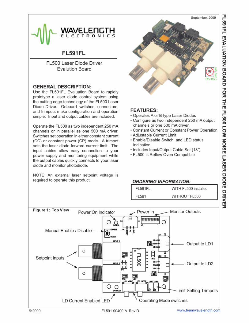
GENERAL DESCRIPTION:Use the FL591FL Evaluation Board to rapidly prototype a laser diode control system using the cutting edge technology of the FL500 Laser Diode Driver. Onboard switches, connectors, and trimpots make confi guration and operation simple. Input and output cables are included.
Operate the FL500 as two independent 250 mA channels or in parallel as one 500 mA driver. Switches set operation in either constant current (CC) or constant power (CP) mode. A trimpot sets the laser diode forward current limit. The input cables allow easy connection to your power supply and monitoring equipment while the output cables quickly connects to your laser diode and monitor photodiode.
NOTE: An external laser setpoint voltage is required to operate this product.
September, 2009
Figure 1: Top View
FL500 Laser Diode Driver Evalution Board
FL591FL
FEATURES:• Operates A or B type Laser Diodes• Confi gure as two independent 250 mA output
channels or one 500 mA driver.• Constant Current or Constant Power Operation• Adjustable Current Limit• Enable/Disable Switch, and LED status
indication• Includes Input/Output Cable Set (18”)• FL500 is Refl ow Oven Compatible
Setpoint Inputs
Manual Enable / Disable
LD Current Enabled LED Operating Mode switches
Limit Setting Trimpots
Output to LD1
Monitor OutputsPower InPower On Indicator
Output to LD2
ORDERING INFORMATION:FL591FL
FL591
WITH FL500 installed
WITHOUT FL500
Pb
RoHS Compliant
www.teamwavelength.com© 2009
FL591FLPAGE 2
FL591-00400-A Rev D
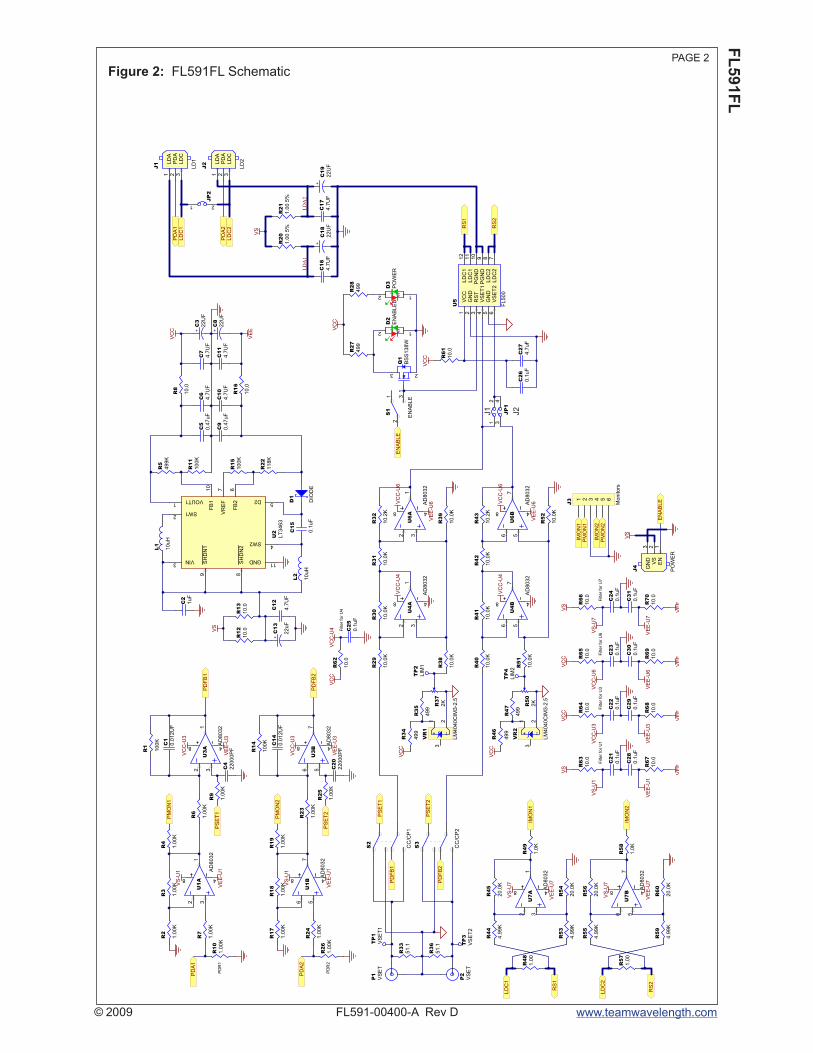
Figure 2: FL591FL Schematic
TH
IS D
RA
WIN
G A
ND
IN
FO
RM
AT
ION
CO
NT
AIN
ED
TH
ER
IN A
RE
TH
E P
RO
PE
RT
Y O
F W
AV
ELE
NG
TH
EL
EC
TR
ON
ICS
, IN
C.
(WE
I). B
Y A
CC
PT
ING
TH
IS
INF
OR
MA
TIO
N,
TH
E B
OR
RO
WE
R A
GR
EE
ES
TH
AT
IT
WIL
L N
OT
BE
US
ED
FO
R A
NY
PU
RP
OS
E O
TH
ER
TH
AN
FO
R W
HIC
H IT
WA
S L
OA
NE
D.
IF T
HE
BO
RR
OW
ER
OF
TH
IS D
OC
UM
EN
T H
AS
NO
T S
IGN
ED
A C
ON
FID
EN
TIA
LIT
Y A
GR
EE
ME
NT
WIT
H W
EI,
TH
E H
E/S
HE
MU
ST
RE
PO
RT
TH
IS F
AC
T T
O W
EI.
FL
500 E
valu
ati
on
Bo
ard
(A
nalo
g -
Lo
ad
ed
)S
IZE
AF
L591-0
0100-B
1
B
SIG
NA
TU
RE
DA
TE
OR
IGIN
AT
OR
EN
GIN
EE
RIN
G
CH
EC
KE
D
AP
PR
OV
ED
TIT
LE
DW
G (
PR
R)
NO
.
SC
AL
ES
HE
ET
RE
V
OF
1
AP
PR
OV
AL
S
J D
Tost
C1
2
4.7
UF
+C
13
22
uF
R1
3
10
.0
R1
2
10
.0
VC
C
R3
3
51
.1
R3
6
51
.1
3
1
2
Q1
BS
S1
38
W
S1
L2
D2
EN
AB
LE
D
VC
C
21 3
S1
EN
AB
LE
RS
2
RS
1
S1
L2
D3
PO
WE
R
R2
8
49
9
R2
1
1.0
0 5
%
C1
7
4.7
UF
+
C1
9
22
UF
LD
C1
LD
C2
R2
7
49
9
R2
9
10
.0K
R3
0
10
.0K
R3
1
10
.0K
R3
2
10
.2K
R3
8
10
.0K
R3
9
10
.0K
VC
C-U
4V
CC
-U6
VE
E-U
6R
37
2K
R3
5
49
9
+1
--2
3
VR
1
LM
40
40
CIM
3-2
.5
R3
4
49
9
VC
C
R4
0
10
.0K
R4
1
10
.0K
R4
2
10
.0K
R4
3
10
.2K
R5
1
10
.0K
R5
2
10
.0K
VC
C-U
4V
CC
-U6
VE
E-U
6
R5
0
2K
R4
7
49
9
+1
--2
3
VR
2
LM
40
40
CIM
3-2
.5
R4
6
49
9
VC
C
2 31
8 4
U4
A
AD
80
32
2 31
8 4
U6
A
AD
80
32
567
8 4
U4
B
AD
80
32
567
8 4
U6
B
AD
80
32
2 31
8 4
U7
A
AD
80
32
567
8 4
U7
B
AD
80
32
2 31
8 4
U1
A
AD
80
32
2 31
8 4
U3
A
AD
80
32
VS
-U7
VS
-U7
R5
9
4.9
9K
R5
5
4.9
9K
R5
6
20
.0K
R4
4
4.9
9K
R5
3
4.9
9K
R4
5
20
.0K
R5
4
20
.0K
R4
9
1.0
K
R6
0
20
.0K
LD
C2
RS
2
LD
C1
RS
1
IMO
N1
IMO
N2
R2
1.0
0K
VE
E-U
1V
EE
-U3
R3
1.0
0K
R7
1.0
0K
PD
A1
VS
-U1
VC
C-U
3
R4
1.0
0K
PM
ON
1
R6
1.0
0K
R1
10
0K
PS
ET
1R
9
1.0
0K
567
8 4
U1
B
AD
80
32
567
8 4
U3
B
AD
80
32
R1
7
1.0
0K
VE
E-U
1V
EE
-U3
R1
8
1.0
0K
R2
4
1.0
0K
PD
A2
VS
-U1
VC
C-U
3
R1
9
1.0
0K
PM
ON
2
R2
3
1.0
0K
R1
4
10
0K
PS
ET
2R
25
1.0
0K
PD
FB
1
PD
FB
2
PD
FB
1
PD
FB
2
PS
ET
1
PS
ET
2
PD
A1
PD
A2
R1
0
1.0
0K
R2
6
1.0
0K
C1
4
0.0
12
UF
C1
0.0
12
UF
C2
0
220
00
PF
C4
220
00
PF
R4
8
1.0
0
R5
7
1.0
0
C9
0.4
7u
F
C5
0.4
7u
F
C2
1uF
C1
5
0.1
uF
L2
10
uH
L1
10
uH
D1
DIO
DE
VIN3
SW12
VOUT11
SH
DN
19
SH
DN
28
GND11
SW24
D25
FB
11
0
VR
EF
7
FB
26
U2
LT
34
63
VC
C
VE
E
R8
10
.0
R1
6
10
.0
C1
0
4.7
UF
C7
4.7
UF
C6
4.7
UF
C1
1
4.7
UF
+C
3
22
UF
+C
8
22
UF
R1
5
10
0K
R1
1
10
0K
R5
49
9K
R5
8
1.0
K
1 2 3 4 5 6
J3
Mo
nito
rs
IMO
N1
IMO
N2
PM
ON
2
PM
ON
1
PD
R1
PD
R2
S2
CC
/CP
1
S3
CC
/CP
2
VE
E-U
7
VE
E-U
7
VC
C1
GN
D2
RS
T3
VS
ET
14
GN
D5
VS
ET
26
LD
C2
7L
DC
28
PG
ND
9P
GN
D1
0L
DC
11
1L
DC
11
2
U5
FL
50
0
LD
C3
PD
A2
LD
A1
J1
LD
1 LD
C3
PD
A2
LD
A1
J2
LD
2
EN
1
GN
D3
VS
2
J4
PO
WE
R
VS
EN
AB
LE
EN
AB
LE
VS
VS
TP
1
VS
ET
1
TP
3
VS
ET
2
TP
4
LIM
2
TP
2
LIM
1
P1
VS
ET
P2
VS
ET
R2
2
11
8K
R2
0
1.0
0 5
%
C1
6
4.7
UF
+
C1
8
22
UF
LD
A2
LD
A1
1 32 4
JP
1
1 2
JP
2
C2
1
0.1
uF
VS
VE
E
C2
5
0.1
uF
VC
C-U
4 Filt
er
for
U4
Filt
er
for
U1
C2
6
0.1
uF
R6
1
10
.0
C2
7
4.7
uF
R6
3
10
.0
VS
-U1
R6
2
10
.0
VC
C
C2
8
0.1
uF
R6
7
10
.0V
EE
-U1
C2
2
0.1
uF
VC
C
VE
E
Filt
er
for
U3
R6
4
10
.0
VC
C-U
3
C2
9
0.1
uF
R6
8
10
.0V
EE
-U3
C2
3
0.1
uF
VC
C
VE
E
Filt
er
for
U6
R6
5
10
.0
VC
C-U
6
C3
0
0.1
uF
R6
9
10
.0V
EE
-U6
C2
4
0.1
uF
VS
VE
E
Filt
er
for
U7
R6
6
10
.0
VS
-U7
C3
1
0.1
uF
R7
0
10
.0V
EE
-U7
20
07
-01
-15
(JD
T)
Ro
lled
to
re
vis
ion
B a
s p
er
EO
#2
08
J1 J2
www.teamwavelength.com© 2009
FL591FLPAGE 3
FL591-00400-A Rev D
Operating LD Current
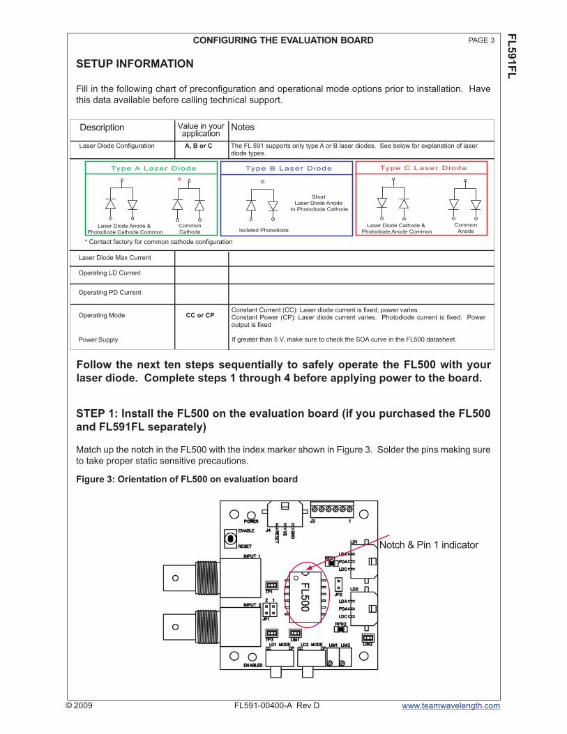
Laser Diode Confi guration A, B or C The FL 591 supports only type A or B laser diodes. See below for explanation of laser diode types.
Laser Diode Max Current
CONFIGURING THE EVALUATION BOARD
STEP 1: Install the FL500 on the evaluation board (if you purchased the FL500 and FL591FL separately)
Match up the notch in the FL500 with the index marker shown in Figure 3. Solder the pins making sure to take proper static sensitive precautions.
SETUP INFORMATION
Fill in the following chart of preconfi guration and operational mode options prior to installation. Have this data available before calling technical support.
Description Value in your application
Notes
Follow the next ten steps sequentially to safely operate the FL500 with your laser diode. Complete steps 1 through 4 before applying power to the board.
Figure 3: Orientation of FL500 on evaluation board
Notch & Pin 1 indicator
Operating PD Current
Operating Mode CC or CP Constant Current (CC): Laser diode current is fi xed, power varies.Constant Power (CP): Laser diode current varies. Photodiode current is fi xed. Power output is fi xed
Power Supply If greater than 5 V, make sure to check the SOA curve in the FL500 datasheet.
Type A Laser D iode Type B Laser D iode Type C Laser D iode
Common
CathodeLaser Diode Anode &
Photodiode Cathode Common Isolated Photodiode
Short
Laser Diode Anode
to Photodiode Cathode
Common
AnodeLaser Diode Cathode &
Photodiode Anode Common
*
* Contact factory for common cathode confi guration
www.teamwavelength.com© 2009
FL591FLPAGE 4
FL591-00400-A Rev D
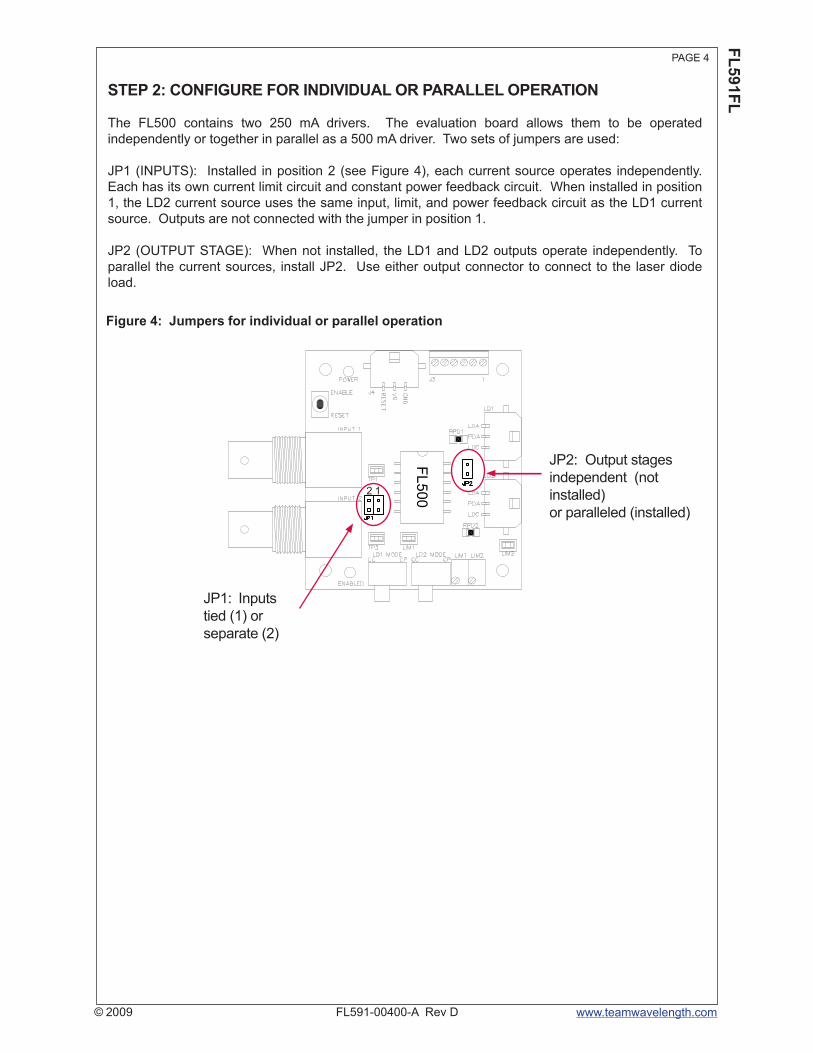
STEP 2: CONFIGURE FOR INDIVIDUAL OR PARALLEL OPERATION
The FL500 contains two 250 mA drivers. The evaluation board allows them to be operated independently or together in parallel as a 500 mA driver. Two sets of jumpers are used:
JP1 (INPUTS): Installed in position 2 (see Figure 4), each current source operates independently. Each has its own current limit circuit and constant power feedback circuit. When installed in position 1, the LD2 current source uses the same input, limit, and power feedback circuit as the LD1 current source. Outputs are not connected with the jumper in position 1.
JP2 (OUTPUT STAGE): When not installed, the LD1 and LD2 outputs operate independently. To parallel the current sources, install JP2. Use either output connector to connect to the laser diode load.
FL500
JP1: Inputs tied (1) or separate (2)
JP2: Output stages independent (not installed) or paralleled (installed)
Figure 4: Jumpers for individual or parallel operation
2 1
www.teamwavelength.com© 2009
FL591FLPAGE 5
FL591-00400-A Rev D
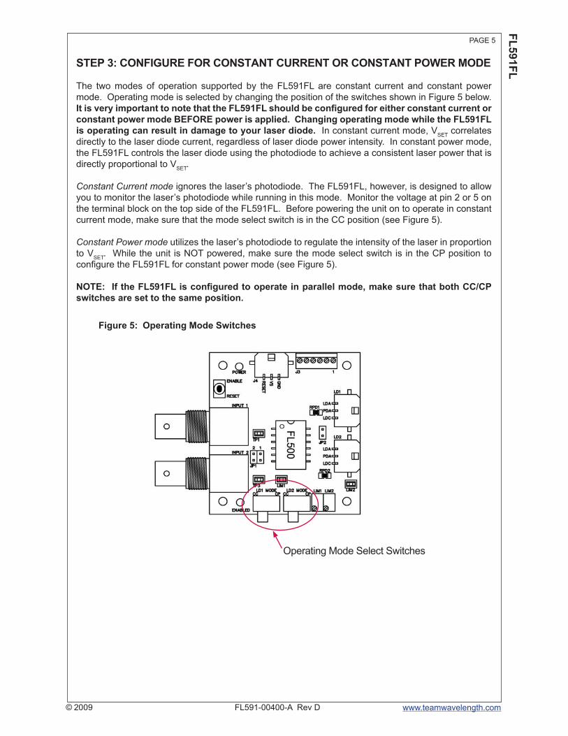
STEP 3: CONFIGURE FOR CONSTANT CURRENT OR CONSTANT POWER MODE
The two modes of operation supported by the FL591FL are constant current and constant power mode. Operating mode is selected by changing the position of the switches shown in Figure 5 below. It is very important to note that the FL591FL should be confi gured for either constant current or constant power mode BEFORE power is applied. Changing operating mode while the FL591FL is operating can result in damage to your laser diode. In constant current mode, VSET correlates directly to the laser diode current, regardless of laser diode power intensity. In constant power mode, the FL591FL controls the laser diode using the photodiode to achieve a consistent laser power that is directly proportional to VSET.
Constant Current mode ignores the laser’s photodiode. The FL591FL, however, is designed to allow you to monitor the laser’s photodiode while running in this mode. Monitor the voltage at pin 2 or 5 on the terminal block on the top side of the FL591FL. Before powering the unit on to operate in constant current mode, make sure that the mode select switch is in the CC position (see Figure 5).
Constant Power mode utilizes the laser’s photodiode to regulate the intensity of the laser in proportion to VSET. While the unit is NOT powered, make sure the mode select switch is in the CP position to confi gure the FL591FL for constant power mode (see Figure 5).
NOTE: If the FL591FL is confi gured to operate in parallel mode, make sure that both CC/CP switches are set to the same position.
Figure 5: Operating Mode Switches
Operating Mode Select Switches
www.teamwavelength.com© 2009
FL591FLPAGE 6
FL591-00400-A Rev D
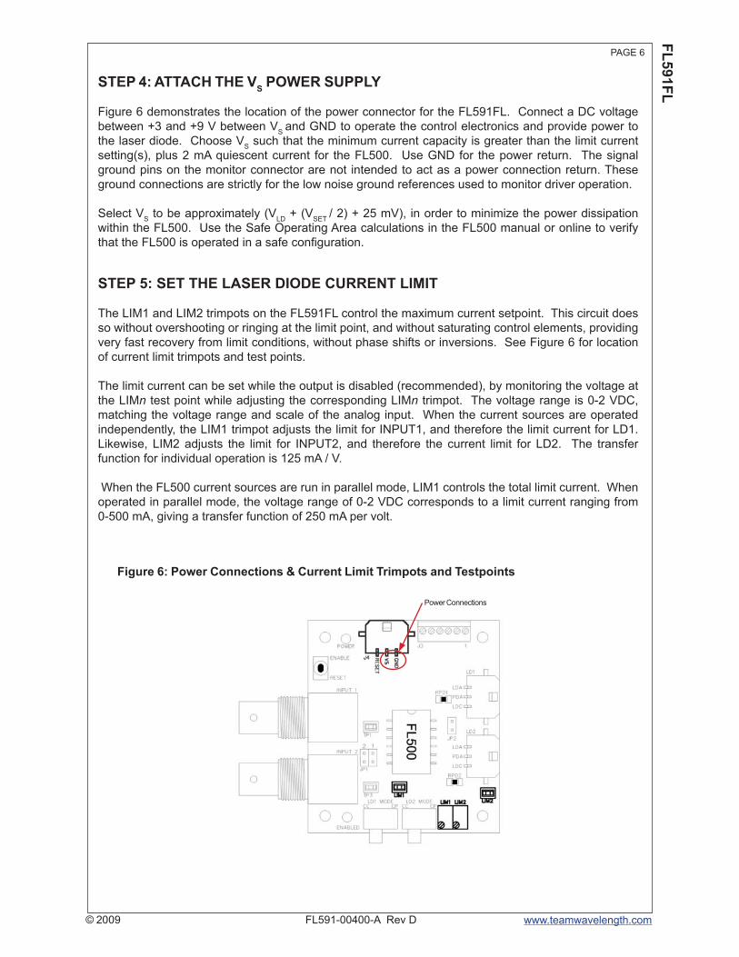
STEP 4: ATTACH THE VS POWER SUPPLY
Figure 6 demonstrates the location of the power connector for the FL591FL. Connect a DC voltage between +3 and +9 V between VS and GND to operate the control electronics and provide power to the laser diode. Choose VS such that the minimum current capacity is greater than the limit current setting(s), plus 2 mA quiescent current for the FL500. Use GND for the power return. The signal ground pins on the monitor connector are not intended to act as a power connection return. These ground connections are strictly for the low noise ground references used to monitor driver operation.
Select VS to be approximately (VLD + (VSET / 2) + 25 mV), in order to minimize the power dissipation within the FL500. Use the Safe Operating Area calculations in the FL500 manual or online to verify that the FL500 is operated in a safe confi guration.
STEP 5: SET THE LASER DIODE CURRENT LIMIT
The LIM1 and LIM2 trimpots on the FL591FL control the maximum current setpoint. This circuit does so without overshooting or ringing at the limit point, and without saturating control elements, providing very fast recovery from limit conditions, without phase shifts or inversions. See Figure 6 for location of current limit trimpots and test points.
The limit current can be set while the output is disabled (recommended), by monitoring the voltage at the LIMn test point while adjusting the corresponding LIMn trimpot. The voltage range is 0-2 VDC, matching the voltage range and scale of the analog input. When the current sources are operated independently, the LIM1 trimpot adjusts the limit for INPUT1, and therefore the limit current for LD1. Likewise, LIM2 adjusts the limit for INPUT2, and therefore the current limit for LD2. The transfer function for individual operation is 125 mA / V.
When the FL500 current sources are run in parallel mode, LIM1 controls the total limit current. When operated in parallel mode, the voltage range of 0-2 VDC corresponds to a limit current ranging from 0-500 mA, giving a transfer function of 250 mA per volt.
Figure 6: Power Connections & Current Limit Trimpots and Testpoints
Power Connections
www.teamwavelength.com© 2009
FL591FLPAGE 7
FL591-00400-A Rev D
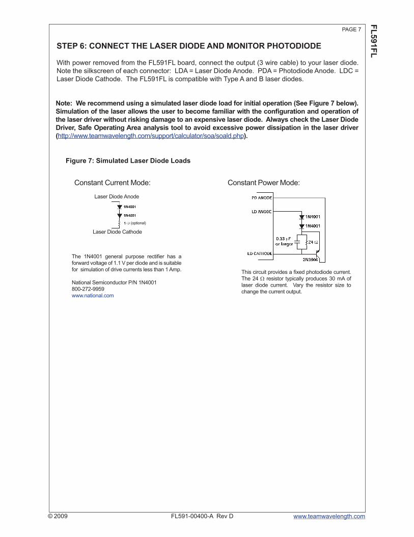
STEP 6: CONNECT THE LASER DIODE AND MONITOR PHOTODIODE
With power removed from the FL591FL board, connect the output (3 wire cable) to your laser diode. Note the silkscreen of each connector: LDA = Laser Diode Anode. PDA = Photodiode Anode. LDC = Laser Diode Cathode. The FL591FL is compatible with Type A and B laser diodes.
Note: We recommend using a simulated laser diode load for initial operation (See Figure 7 below). Simulation of the laser allows the user to become familiar with the confi guration and operation of the laser driver without risking damage to an expensive laser diode. Always check the Laser Diode Driver, Safe Operating Area analysis tool to avoid excessive power dissipation in the laser driver (http://www.teamwavelength.com/support/calculator/soa/soald.php).
Constant Current Mode:
Laser Diode Anode
Laser Diode Cathode
Constant Power Mode:
The 1N4001 general purpose rectifi er has a forward voltage of 1.1 V per diode and is suitable for simulation of drive currents less than 1 Amp.
National Semiconductor P/N 1N4001800-272-9959www.national.com
This circuit provides a fi xed photodiode current. The 24 Ω resistor typically produces 30 mA of laser diode current. Vary the resistor size to change the current output.
(optional)
Figure 7: Simulated Laser Diode Loads
www.teamwavelength.com© 2009
FL591FLPAGE 8
FL591-00400-A Rev D
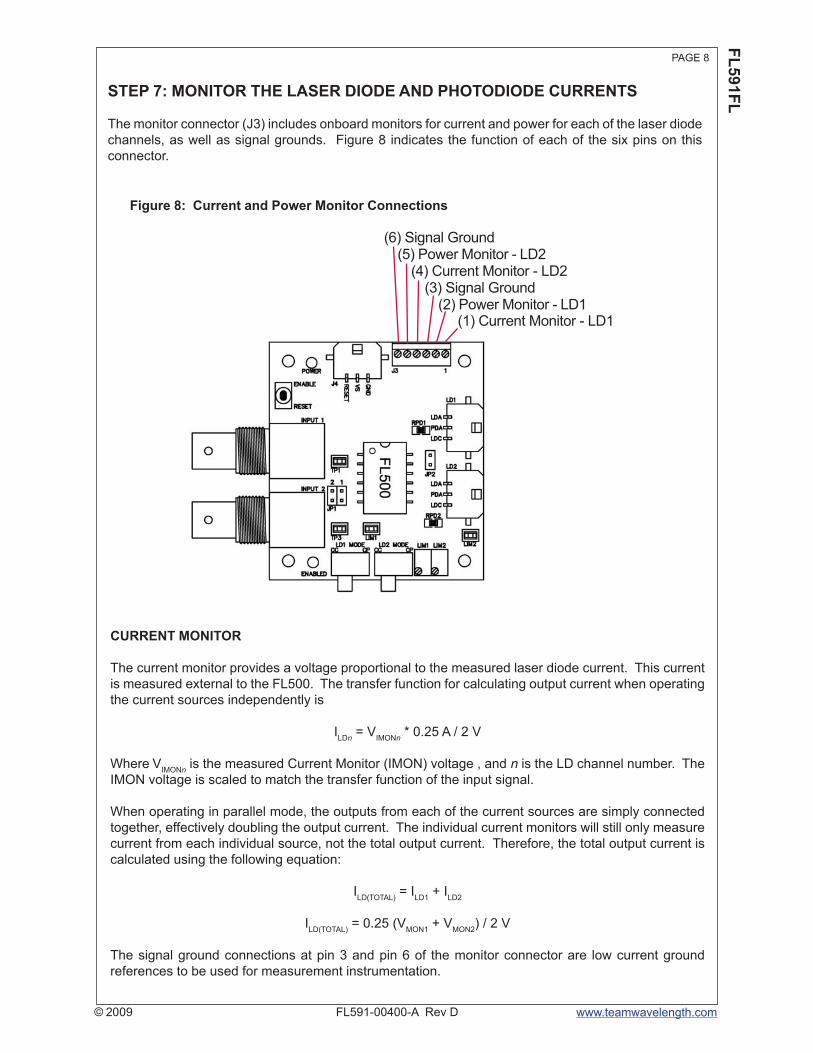
STEP 7: MONITOR THE LASER DIODE AND PHOTODIODE CURRENTS
The monitor connector (J3) includes onboard monitors for current and power for each of the laser diode channels, as well as signal grounds. Figure 8 indicates the function of each of the six pins on this connector.
(1) Current Monitor - LD1(2) Power Monitor - LD1
(3) Signal Ground(4) Current Monitor - LD2
(5) Power Monitor - LD2(6) Signal Ground
CURRENT MONITOR
The current monitor provides a voltage proportional to the measured laser diode current. This current is measured external to the FL500. The transfer function for calculating output current when operating the current sources independently is
ILDn = VIMONn * 0.25 A / 2 V
Where VIMONn is the measured Current Monitor (IMON) voltage , and n is the LD channel number. The IMON voltage is scaled to match the transfer function of the input signal.
When operating in parallel mode, the outputs from each of the current sources are simply connected together, effectively doubling the output current. The individual current monitors will still only measure current from each individual source, not the total output current. Therefore, the total output current is calculated using the following equation:
ILD(TOTAL) = ILD1 + ILD2
ILD(TOTAL) = 0.25 (VMON1 + VMON2) / 2 V
The signal ground connections at pin 3 and pin 6 of the monitor connector are low current ground references to be used for measurement instrumentation.
Figure 8: Current and Power Monitor Connections
www.teamwavelength.com© 2009
FL591FLPAGE 9
FL591-00400-A Rev D
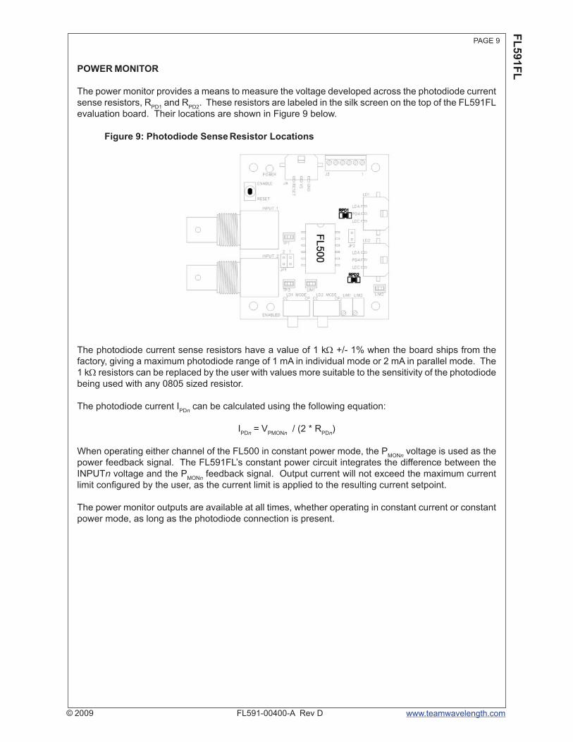
POWER MONITOR
The power monitor provides a means to measure the voltage developed across the photodiode current sense resistors, RPD1 and RPD2. These resistors are labeled in the silk screen on the top of the FL591FL evaluation board. Their locations are shown in Figure 9 below.
The photodiode current sense resistors have a value of 1 kΩ +/- 1% when the board ships from the factory, giving a maximum photodiode range of 1 mA in individual mode or 2 mA in parallel mode. The 1 kΩ resistors can be replaced by the user with values more suitable to the sensitivity of the photodiode being used with any 0805 sized resistor.
The photodiode current IPDn can be calculated using the following equation:
IPDn = VPMONn / (2 * RPDn)
When operating either channel of the FL500 in constant power mode, the PMONn voltage is used as the power feedback signal. The FL591FL’s constant power circuit integrates the difference between the INPUTn voltage and the PMONn feedback signal. Output current will not exceed the maximum current limit confi gured by the user, as the current limit is applied to the resulting current setpoint.
The power monitor outputs are available at all times, whether operating in constant current or constant power mode, as long as the photodiode connection is present.
Figure 9: Photodiode Sense Resistor Locations
www.teamwavelength.com© 2009
FL591FLPAGE 10
FL591-00400-A Rev D
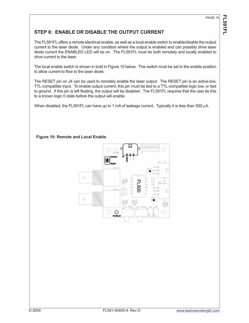
STEP 8: ENABLE OR DISABLE THE OUTPUT CURRENT
The FL591FL offers a remote electrical enable, as well as a local enable switch to enable/disable the output current to the laser diode. Under any condition where the output is enabled and can possibly drive laser diode current the ENABLED LED will be on. The FL591FL must be both remotely and locally enabled to drive current to the laser.
The local enable switch is shown in bold in Figure 10 below. This switch must be set to the enable position to allow current to fl ow to the laser diode.
The RESET pin on J4 can be used to remotely enable the laser output. The RESET pin is an active-low, TTL-compatible input. To enable output current, this pin must be tied to a TTL-compatible logic low, or tied to ground. If this pin is left fl oating, the output will be disabled. The FL591FL requires that the user tie this to a known logic 0 state before the output will enable.
When disabled, the FL591FL can have up to 1 mA of leakage current. Typically it is less than 500 μA.
Figure 10: Remote and Local Enable
www.teamwavelength.com© 2009
FL591FLPAGE 11
FL591-00400-A Rev D
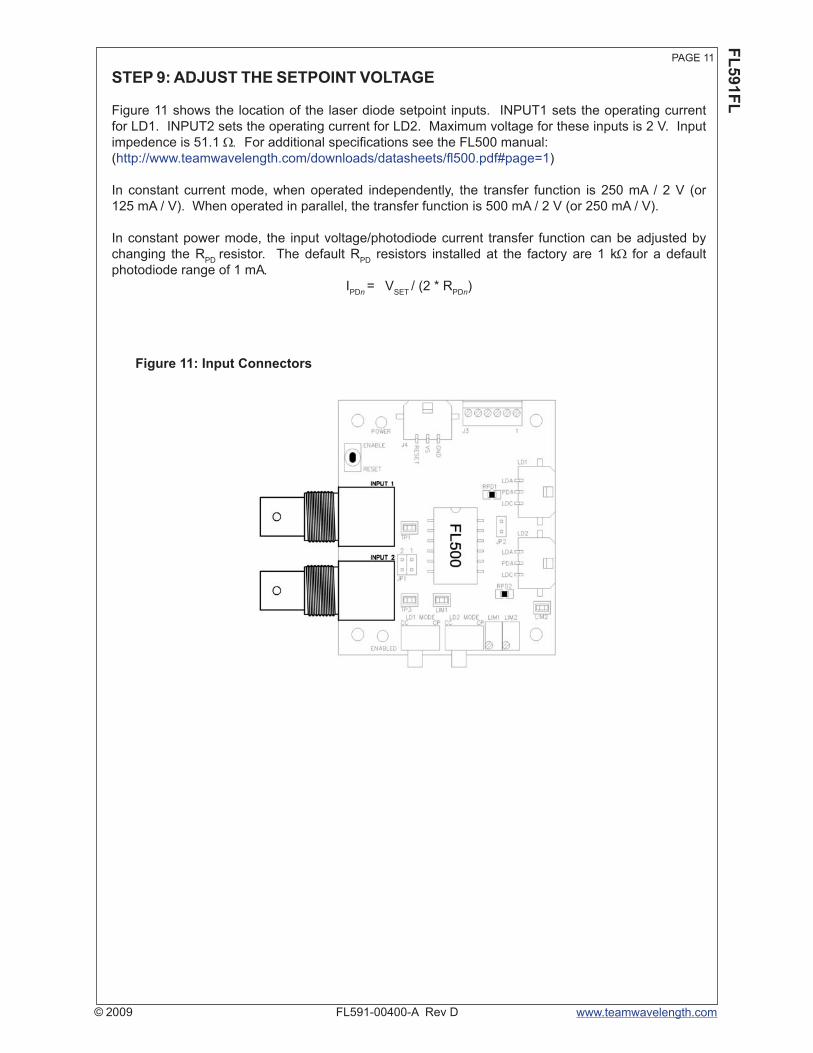
STEP 9: ADJUST THE SETPOINT VOLTAGE
Figure 11 shows the location of the laser diode setpoint inputs. INPUT1 sets the operating current for LD1. INPUT2 sets the operating current for LD2. Maximum voltage for these inputs is 2 V. Input impedence is 51.1 Ω. For additional specifi cations see the FL500 manual: (http://www.teamwavelength.com/downloads/datasheets/fl 500.pdf#page=1)
In constant current mode, when operated independently, the transfer function is 250 mA / 2 V (or 125 mA / V). When operated in parallel, the transfer function is 500 mA / 2 V (or 250 mA / V).
In constant power mode, the input voltage/photodiode current transfer function can be adjusted by changing the RPD resistor. The default RPD resistors installed at the factory are 1 kΩ for a default photodiode range of 1 mA.
IPDn = VSET / (2 * RPDn)
Figure 11: Input Connectors
www.teamwavelength.com© 2009
FL591FLPAGE 12
FL591-00400-A Rev D
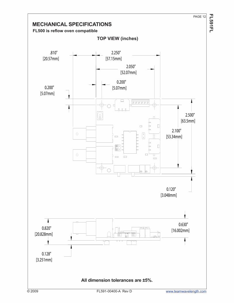
TOP VIEW (inches)
MECHANICAL SPECIFICATIONS
[16.002mm]0.630"
[3.251mm]0.128"
[20.828mm]0.820"
[5.07mm]0.200" [5.07mm]
0.200"
[52.07mm]2.050"
[57.15mm]2.250"
[20.57mm].810"
[53.34mm]2.100"
[63.5mm]2.500"
[3.048mm]0.120"
All dimension tolerances are ±5%.
FL500 is refl ow oven compatible
www.teamwavelength.com© 2009
FL591FLPAGE 13
FL591-00400-A Rev D
WAVELENGTH ELECTRONICS, INC.51 Evergreen Drive Bozeman, Montana, 59715
phone: (406) 587-4910 Sales and Technical Supportfax: (406) 587-4911e-mail: [email protected]: www.teamwavelength.com
NOTICE: The information contained in this document is subject to change without notice. Wavelength will not be liable for errors contained herein or for incidental or consequential damages in connection with the furnishing, performance, or use of this material. No part of this document may be photocopied, reproduced, or translated to another language without the prior written consent of Wavelength.
SAFETY:There are no user serviceable parts inside this product. Return the product to Wavelength for ser-vice and repair to ensure that safety features are maintained.
LIFE SUPPORT POLICY:As a general policy, Wavelength Electronics, Inc. does not recommend the use of any of its products in life support applications where the failure or malfunction of the Wavelength product can be reasonably expected to cause failure of the life support device or to signifi cantly affect its safety or effectiveness. Wavelength will not knowingly sell its products for use in such applications unless it receives written assurances satisfactory to Wavelength that the risks of injury or damage have been minimized, the customer assumes all such risks, and there is no product liability for Wavelength. Examples of devices considered to be life support devices are neonatal oxygen analyzers, nerve stimulators (for any use), auto transfusion devices, blood pumps, defi brillators, arrhythmia detectors and alarms, pacemakers, hemodialysis systems, peritoneal dialysis systems, ventilators of all types, and infusion pumps as well as other devices designated as “critical” by the FDA. The above are representative examples only and are not intended to be conclusive or exclusive of any other life support device.
CERTIFICATION AND WARRANTYCERTIFICATION:Wavelength Electronics (Wavelength) certifi es that this product met it’s published specifi cations at the time of shipment. Wavelength further certifi es that its calibration measurements are traceable to the United States National Institute of Standards and Technology, to the extent allowed by that organization’s calibration facilities, and to the calibration facilities of other International Standards Organization members.
WARRANTY:This Wavelength product is warranted against defects in materials and workmanship for a period of 90 days from date of shipment. During the warranty period, Wavelength will, at its option, either repair or replace products which prove to be defective.
WARRANTY SERVICE:For warranty service or repair, this product must be returned to the factory. An RMA is required for products returned to Wavelength for warranty service. The Buyer shall prepay shipping charges to Wavelength and Wavelength shall pay shipping charges to return the product to the Buyer upon determination of defective materials or workmanship. However, the Buyer shall pay all shipping charges, duties, and taxes for products returned to Wavelength from another country.
LIMITATIONS OF WARRANTY:The warranty shall not apply to defects resulting from improper use or misuse of the product or operation outside published specifi cations.
No other warranty is expressed or implied. Wavelength specifi cally disclaims the implied warranties of merchantability and fi tness for a particular purpose.
EXCLUSIVE REMEDIES:The remedies provided herein are the Buyer’s sole and exclusive remedies. Wavelength shall not be liable for any direct, indirect, special, incidental, or consequential damages, whether based on contract, tort, or any other legal theory.
REVISION HISTORYREVISIONREV. BREV. C
REV. D
DATEJul-06
17-Feb-09
25-Sep-09
NOTESInitial release
Updated to include FL500 Refl ow Oven compatibility
Updated to refl ect RoHS compliance