fl500 dual channel laser diode driver datasheet · pdf filefl500 smt driver for laser diodes...
TRANSCRIPT
FL500 SMT D
RIVER
FOR
LASER
DIO
DES
www.teamWavelength.com© 2015 FL500-00400-K
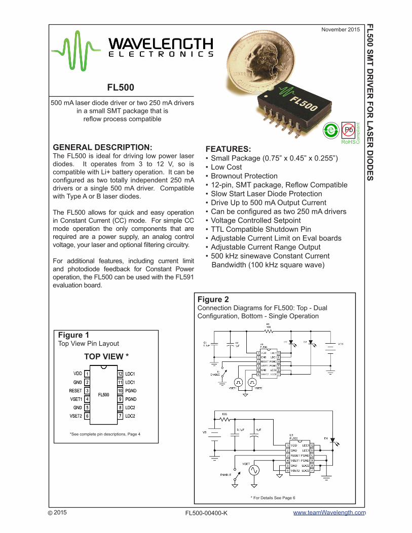
TOP VIEW *
GENERAL DESCRIPTION:The FL500 is ideal for driving low power laser diodes. It operates from 3 to 12 V, so is compatible with Li+ battery operation. It can be configured as two totally independent 250 mA drivers or a single 500 mA driver. Compatible with Type A or B laser diodes.
The FL500 allows for quick and easy operation in Constant Current (CC) mode. For simple CC mode operation the only components that are required are a power supply, an analog control voltage, your laser and optional filtering circuitry.
For additional features, including current limit and photodiode feedback for Constant Power operation, the FL500 can be used with the FL591 evaluation board.
500 mA laser diode driver or two 250 mA drivers in a small SMT package that is
reflow process compatible
FEATURES:• Small Package (0.75” x 0.45” x 0.255”)• Low Cost• Brownout Protection• 12-pin, SMT package, Reflow Compatible• Slow Start Laser Diode Protection• Drive Up to 500 mA Output Current• Can be configured as two 250 mA drivers• Voltage Controlled Setpoint• TTL Compatible Shutdown Pin• Adjustable Current Limit on Eval boards• Adjustable Current Range Output• 500 kHz sinewave Constant Current
Bandwidth (100 kHz square wave)
November 2015
Figure 1Top View Pin Layout
FL500
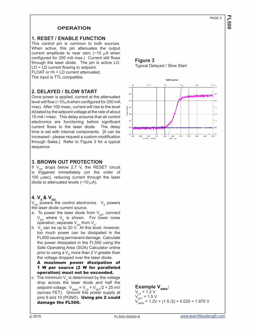
* For Details See Page 6
Figure 2Connection Diagrams for FL500: Top - Dual Configuration, Bottom - Single Operation
*See complete pin descriptions, Page 4
Pb
RoHS Com
plia
nte

www.teamWavelength.com© 2015
FL500PAGE 2
FL500-00400-K
BLOCK DIAGRAM
VDD GND
RESET(Active Low,
TTL compatible)
VSET 1
VSET 2(Impedance:
2kΩ per driver, 1kΩ when paralleled) LDC2
LDC2
PWR GND (for LD VS)
PWR GND (for LD VS)
LDC1
LDC1
VS
SUPPORTS A & B LASER DIODE PACKAGE STYLES
GND (for VSET)
LD
Type A Laser Diode Type B Laser Diode Type C Laser Diode
CommonCathode
Laser Diode Anode & Photodiode Cathode Common Isolated Photodiode
Short Laser Diode Anode
to Photodiode CathodeCommon
AnodeLaser Diode Cathode &
Photodiode Anode Common
* Contact factory for common cathode configuration

www.teamWavelength.com© 2015
FL500PAGE 3
FL500-00400-K
Supply Voltage (Voltage on Pin 1)Output Current (See SOA Chart)Power Dissipation, TAMBIENT = +25˚C [1]Operating Temperature, case Storage TemperatureWeight
ELECTRICAL AND OPERATING SPECIFICATIONS
Volts DCmAWatts˚C˚Coz
UNITVALUE
50
245495VDD- (0.5 x Vset
100
32.2
0-1660
+3 to +12 **5002- 40 to + 85- 55 to +1250.08
VDD
IOUT
PMAX
TOPR
TSTG
FL500
ABSOLUTE MAXIMUM RATINGSRATING SYMBOL
ppmppm
%%
mAmA
VoltsnsecnseckHzkHz
msecmA / msec
%A / VA / V
VoltsmA
Volts
mVnAV
dBdB
˚C / WSec
µAµAµAµA
4075
252505
)
12**4.620**
15VDD
35
0.0190.011
250 500
300 300 500 100
15 99
0.125 0.25
2.7
210
64
4310
350
100150
CONSTANT CURRENT CONTROLShort Term Stability, 1 hourLong Term Stability, 24 hoursCONSTANT POWER CONTROL Short Term Stability, 1 hour [3]Long Term Stability, 24 hours [3]OUTPUT [2]Current, peak, see SOA chartCurrent, peak, see SOA chartCompliance Voltage, Laser Diode LoadRise TimeFall TimeBandwidthBandwidthDelayed startSlow Start ramp rateDepth of ModulationTransfer Function - VSET to IOUT
Transfer Function - VSET to IOUT
POWER SUPPLYVoltage, VDD
Current, VDD supply, quiescentVS, Maximum to LD AnodeINPUTOffset Voltage, initial, Imon
Bias Current (based on input Res of op amp)
Common Mode RangeCommon Mode Rejection, Set pointPower Supply RejectionTHERMALHeatspreader Temperature RisePin SolderabilityNOISENoise & Ripple (Rms)Leakage Current (when using the FL591 circuitry)
TYPMIN MAX UNITSTEST CONDITIONSPARAMETER
TAMBIENT = 25˚CTAMBIENT = 25˚C
Per channelTwo channels operated in parallelFull Temp. Range, IOUT = 500 mAIOUT= 500 mAIOUT= 500 mAConstant Current, Sine WaveConstant Current, Square Wave
100 kHz sine waveConfigured as two 250 mA driversConfigured as one 500 mA driver
Pin 2, TAMBIENT = 25˚C, VCM = 0 VPin 2, TAMBIENT = 25˚C, VCM = 0 VPin 2, Full Temp. RangeFull Temperature RangeFull Temperature Range
TAMBIENT = 25˚CSolder temp @260˚C
IOUT = 100 mA, 100 kHz bandwidthVSET = 0 VVSET = 1 VVSET = 2 V
**The FL591 Evaluation Board revision A or B limits the input voltage to 9 V. Revision C allows full range operation from +3 V to +12 V.

www.teamWavelength.com© 2015
FL500PAGE 4
FL500-00400-K
Power supply input for the FL500’s internal control electronics.Supply range input for this pin is +3 to +12 Volts DC. It is compatible with Li+ batteries.Return path for control electronics. Connect ground for VDD power supply here. Do not use for high current ground return.TTL compatible. LO = laser diode current onFLOAT or HI = laser diode current attenuated to ~10 µA (~20 µA if drivers are paralleled to produce 500 mA)2 kΩ input impedance. 0 to 2 V range. There is no internal clamping, so higher voltage here will produce more current through the laser diode. Not recommended above 2 V.Low Current, Low Noise ground for use with VSET1 & VSET2.2 kΩ input impedance. 0 to 2 V range. There is no internal clamping, so higher voltage here will produce more current through the laser diode. Not recommended above 2 V.Tie to laser diode cathode for individual drive operation (250 mA max). Tie to LDC1 for parallel operation up to 500 mA. Tie to pin 8 (also LDC2) if laser diode current exceeds 125 mA. Actual pin capacity is greater, but higher current produces offsets and higher noise.Use for ground connection of VS power supply. Tie to pin 10 (also PGND) if laser diode current exceeds 125 mA.Tie to laser diode cathode for individual drive operation (250 mA max). Tie to LDC2 for parallel operation up to 500 mA. Tie to pin 12 (also LDC1) if laser diode current exceeds 125 mA. Actual pin capacity is greater, but higher current produces offsets and higher noise.
PIN DESCRIPTIONS
Control Electronics Power
Control Electronics Ground
Enable / RESET Control
Setpoint for LDC1 control
Ground for setpoint inputsSetpoint for LDC2 control
Laser Diode Cathode, Driver 2
Power Ground for VS connectionLaser Diode Cathode, Driver 1
VDD
GND
RESET
VSET1
GNDVSET2
LDC2LDC2
PGNDPGNDLDC1LDC1
1
2
3
4
56
78
9101112
Pin Pin # Name Function
Note [1]. Maximum Power Dissipation is 1 Watt per channel. When configured as one driver, maximum power dissipation is 2 W.Note [2]. Limit is fixed at 500 mA (250 mA per channel). The Evaluation Board circuitry adds a variable limit circuit.Note [3]. Constant Power Control is available when the FL500 is used with FL591 and FL593 as well as the LDTC0520/1020 combination boards.
www.teamWavelength.com© 2015
FL500PAGE 5
FL500-00400-K
1. RESET / ENABLE FUNCTIONThis control pin is common to both sources. When active, this pin attenuates the output current amplitude to near zero (~10 µA when configured for 250 mA max.) Current still flows through the laser diode. The pin is active LO. LO = LD current flowing to setpoint. FLOAT or HI = LD current attenuated. The input is TTL compatible.
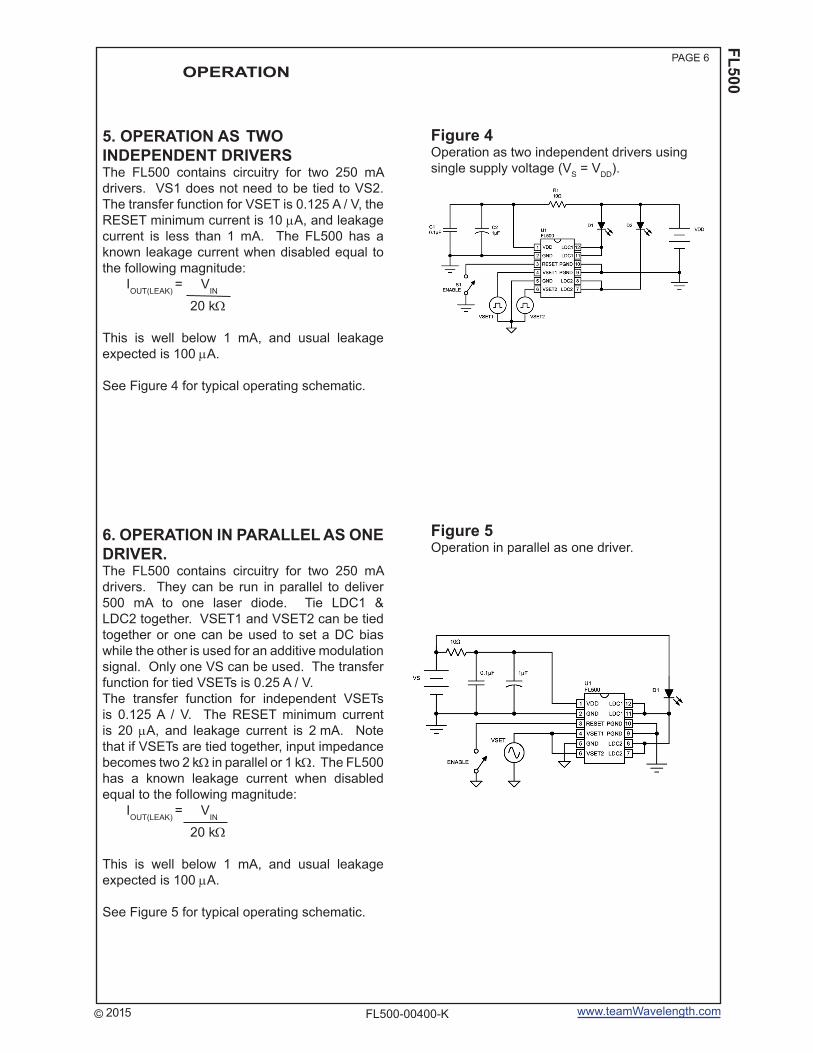
2. DELAYED / SLOW STARTOnce power is applied, current at the attenuated level will flow (~10 µA when configured for 250 mA max). After 100 msec, current will rise to the level dictated by the setpoint voltage at the rate of about 15 mA / msec. This delay ensures that all control electronics are functioning before significant current flows to the laser diode. The delay time is set with internal components. [It can be increased - please request a custom modification through Sales.] Refer to Figure 3 for a typical sequence.
3. BROWN OUT PROTECTIONIf VDD drops below 2.7 V, the RESET circuit is triggered immediately (on the order of 100 µsec), reducing current through the laser diode to attenuated levels (~10 µA).
4. VS & VDDV
DD powers the control electronics. V
S powers
the laser diode current source. a. To power the laser diode from V
DD, connect
VDD
where VS is shown. For lower noise
operation, separate VDD
from VS.
b. VS can be up to 20 V. At this level, however,
too much power can be dissipated in the FL500 causing permanent damage. Calculate the power dissipated in the FL500 using the Safe Operating Area (SOA) Calculator online prior to using a VS more than 2 V greater than the voltage dropped over the laser diode.
A maximum power dissipation of 1 W per source (2 W for paralleled operation) must not be exceeded.
c. The minimum VS is determined by the voltage
drop across the laser diode and half the setpoint voltage. V
SMIN = V
LD + V
SET/2 + 25 mV
(across FET). Ground this power supply at pins 9 and 10 (PGND). Using pin 2 could damage the FL500.
Figure 3Typical Delayed / Slow Start
OPERATION
Example VSMIN:VLD = 1.2 VVSET = 1.5 VVSMIN = 1.2V + (1.5 /2) + 0.025 = 1.975 V
www.teamWavelength.com© 2015
FL500PAGE 6
FL500-00400-K
OPERATION
5. OPERATION AS TWO INDEPENDENT DRIVERSThe FL500 contains circuitry for two 250 mA drivers. VS1 does not need to be tied to VS2. The transfer function for VSET is 0.125 A / V, the RESET minimum current is 10 µA, and leakage current is less than 1 mA. The FL500 has a known leakage current when disabled equal to the following magnitude:
IOUT(LEAK)
= VIN
20 kΩ
This is well below 1 mA, and usual leakage expected is 100 µA.
See Figure 4 for typical operating schematic.
6. OPERATION IN PARALLEL AS ONE DRIVER.The FL500 contains circuitry for two 250 mA drivers. They can be run in parallel to deliver 500 mA to one laser diode. Tie LDC1 & LDC2 together. VSET1 and VSET2 can be tied together or one can be used to set a DC bias while the other is used for an additive modulation signal. Only one VS can be used. The transfer function for tied VSETs is 0.25 A / V. The transfer function for independent VSETs is 0.125 A / V. The RESET minimum current is 20 µA, and leakage current is 2 mA. Note that if VSETs are tied together, input impedance becomes two 2 kΩ in parallel or 1 kΩ. The FL500 has a known leakage current when disabled equal to the following magnitude:
IOUT(LEAK)
= VIN
20 kΩ
This is well below 1 mA, and usual leakage expected is 100 µA.
See Figure 5 for typical operating schematic.
Figure 4Operation as two independent drivers using single supply voltage (VS = VDD).
Figure 5Operation in parallel as one driver.
www.teamWavelength.com© 2015
FL500PAGE 7
FL500-00400-K
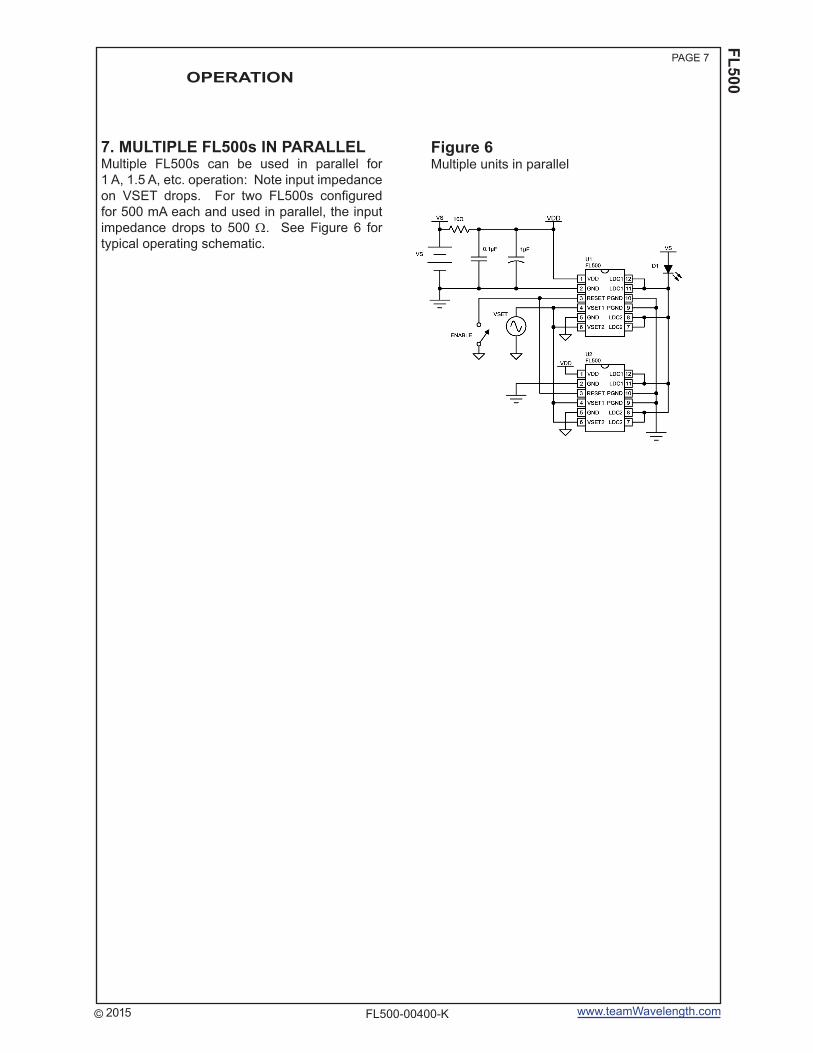
7. MULTIPLE FL500s IN PARALLELMultiple FL500s can be used in parallel for 1 A, 1.5 A, etc. operation: Note input impedance on VSET drops. For two FL500s configured for 500 mA each and used in parallel, the input impedance drops to 500 Ω. See Figure 6 for typical operating schematic.
Figure 6Multiple units in parallel
OPERATION

www.teamWavelength.com© 2015
FL500PAGE 8
FL500-00400-K
TYPICAL PERFORMANCE GRAPH FOR 1 WATT, 250 mA
Caution:Do not exceed the Safe Operating Area (SOA). Exceeding the SOA voids the warranty.
To determine if the operating parameters fall within the SOA of the device, the maximum voltage drop across the driver and the maximum current must be plotted on the SOA curves.These values are used for the example SOA determination:
Vs = 5 voltsVLoad = 2.5 voltsILoad = 100 mA
Follow these steps:1. Determine the maximum voltage drop across the driver,Vs-VLoad, and mark on the X axis. Example: 5 volts - 2.5 volts = 2.5 volts, Point A)2. Determine the maximum current, ILoad, through the driver and mark on the Y axis: (100 mA, Point B)3. Draw a horizontal line through Point B across the chart. (Line BB)4. Draw a vertical line from Point A to the maximum current line indicated by Line BB.5. Mark VS on the X axis. (Point C)6. Draw the Load Line from where the vertical line from point A intersects Line BB down to Point C.
Refer to the chart shown below and note that the Load Line is in the Safe Operating Area. Note the first chart is for the independent channels. The second, on the following page, is for dual channels configured as a single 500 mA driver.
An online tool for calculating your load line is at http://www.teamwavelength.com/support/calculator/soa/soald.php.
These values are determined from the specifications of the laser diode.
Graphs assume:25°C Ambient35°C Case
A
B BB
C
www.teamWavelength.com© 2015
FL500PAGE 9
FL500-00400-K
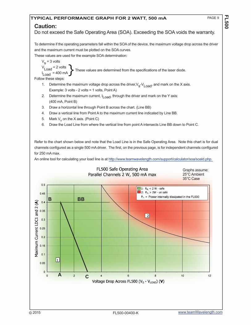
TYPICAL PERFORMANCE GRAPH FOR 2 WATT, 500 mA
Caution:Do not exceed the Safe Operating Area (SOA). Exceeding the SOA voids the warranty.
To determine if the operating parameters fall within the SOA of the device, the maximum voltage drop across the driver and the maximum current must be plotted on the SOA curves.These values are used for the example SOA determination:
Vs = 3 voltsVLoad = 2 voltsILoad = 400 mA
Follow these steps:1. Determine the maximum voltage drop across the driver,Vs-VLoad, and mark on the X axis. Example: 3 volts - 2 volts = 1 volts, Point A)2. Determine the maximum current, ILoad, through the driver and mark on the Y axis: (400 mA, Point B)3. Draw a horizontal line through Point B across the chart. (Line BB)4. Draw a vertical line from Point A to the maximum current line indicated by Line BB.5. Mark VS on the X axis. (Point C)6. Draw the Load Line from where the vertical line from point A intersects Line BB down to Point C.
Refer to the chart shown below and note that the Load Line is in the Safe Operating Area. Note this chart is for dual channels configured as a single 500 mA driver. The first, on the previous page, is for independent channels configured for 250 mA max.An online tool for calculating your load line is at http://www.teamwavelength.com/support/calculator/soa/soald.php.
These values are determined from the specifications of the laser diode.
Graphs assume:25°C Ambient35°C Case
A
BB
C
B
www.teamWavelength.com© 2015
FL500PAGE 10
FL500-00400-K
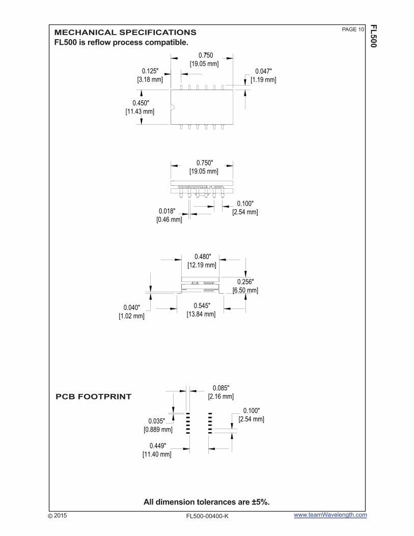
MECHANICAL SPECIFICATIONS
[12.19 mm]0.480"
[6.50 mm]0.256"
[13.84 mm]0.545"
[1.02 mm]0.040"
[2.54 mm]0.100"
[19.05 mm]0.750"
[0.46 mm]0.018"
[3.18 mm]0.125"
[11.43 mm]0.450"
0.750"[19.05 mm]
[1.19 mm]0.047"
[2.54 mm]0.100"
[11.40 mm]0.449"
[0.889 mm]0.035"
[2.16 mm]0.085"
PCB FOOTPRINT
All dimension tolerances are ±5%.
FL500 is reflow process compatible.
www.teamWavelength.com© 2015
FL500PAGE 11
FL500-00400-K
WAVELENGTH ELECTRONICS, INC.51 Evergreen Drive Bozeman, Montana, 59715phone: (406) 587-4910 Sales and Technical Supportfax: (406) 587-4911e-mail: [email protected]: www.teamwavelength.com
NOTICE: The information contained in this document is subject to change without notice. Wavelength will not be liable for errors contained herein or for incidental or consequential damages in connection with the furnishing, performance, or use of this material. No part of this document may be translated to another language without the prior written consent of Wavelength.
SAFETY:There are no user serviceable parts inside this product. Return the product to Wavelength Electronics for service and repair to ensure that safety features are maintained.
LIFE SUPPORT POLICY:As a general policy, Wavelength Electronics, Inc. does not recommend the use of any of its products in life support applications where the failure or malfunction of the Wavelength product can be reasonably expected to cause failure of the life support device or to significantly affect its safety or effectiveness. Wavelength will not knowingly sell its products for use in such applications unless it receives written assurances satisfactory to Wavelength that the risks of injury or damage have been minimized, the customer assumes all such risks, and there is no product liability for Wavelength. Examples of devices considered to be life support devices are neonatal oxygen analyzers, nerve stimulators (for any use), auto transfusion devices, blood pumps, defibrillators, arrhythmia detectors and alarms, pacemakers, hemodialysis systems, peritoneal dialysis systems, ventilators of all types, and infusion pumps as well as other devices designated as “critical” by the FDA. The above are representative examples only and are not intended to be conclusive or exclusive of any other life support device.
CERTIFICATION AND WARRANTYCERTIFICATION:Wavelength Electronics (Wavelength) certifies that this product met it’s published specifications at the time of shipment. Wavelength further certifies that its calibration measurements are traceable to the United States National Institute of Standards and Technology, to the extent allowed by that organization’s calibration facilities, and to the calibration facilities of other International Standards Organization members.
WARRANTY:This Wavelength product is warranted against defects in materials and workmanship for a period of one (1) year from date of shipment. During the warranty period, Wavelength will, at its option, either repair or replace products which prove to be defective.
WARRANTY SERVICE:For warranty service or repair, this product must be returned to the factory. An RMA is required for products returned to Wavelength for warranty service. The Buyer shall prepay shipping charges to Wavelength and Wavelength shall pay shipping charges to return the product to the Buyer upon determination of defective materials or workmanship. However, the Buyer shall pay all shipping charges, duties, and taxes for products returned to Wavelength from another country.
LIMITATIONS OF WARRANTY:The warranty shall not apply to defects resulting from improper use or misuse of the product or operation outside published specifications.
No other warranty is expressed or implied. Wavelength specifically disclaims the implied warranties of merchantability and fitness for a particular purpose.
EXCLUSIVE REMEDIES:The remedies provided herein are the Buyer’s sole and exclusive remedies. Wavelength shall not be liable for any direct, indirect, special, incidental, or consequential damages, whether based on contract, tort, or any other legal theory.
REVERSE ENGINEERING PROHIBITED:Buyer, End-User, or Third-Party Reseller are expressly prohibited from reverse engineering, decompiling, or disassembling this product.
REVISION HISTORYREVISIONREV. F
REV. G
REV. H
REV. I
REV. J
REV. K
DATE24-Feb-09
25-Sep-09
6-June-13
26-Mar-14
15-Dec-14
Nov. 2015
NOTESUpdated to include FL500 Reflow Oven compatibility
Updated to reflect RoHS Status
Updated Noise & Ripple specification
Clarified reflow compatibility
Updated to fully reflow compatible
Updated leakage current spec