floating switch for offline ac linear direct drive of … · vin rset tps92411 rsns drain vs vin...
TRANSCRIPT

VIN
RSET
TPS92411
RSNS
DRAIN
VS
VIN
RSET
TPS92411
RSNS
DRAIN
VS
VIN
RSET
TPS92411
RSNS
DRAIN
VS
± +
120 VRMS
Product
Folder
Sample &Buy
Technical
Documents
Tools &
Software
Support &Community
TPS92411, TPS92411PSLUSBQ6B –OCTOBER 2013–REVISED JULY 2014
TPS92411x Floating Switch for Offline AC Linear Direct Drive of LEDs with Low RippleCurrent
1 FeaturesDevice Information(1)
1• High-Performance Solution for Driving LEDs fromPART NUMBER PACKAGE BODY SIZE (NOM)AC Mains
SOT-23 (5) 2.90 mm x 1.60 mmTPS92411,• Simplifies Design of Phase Dimmable LED Driver TPS92411P SO PowerPAD (8) 4.89 mm x 3.90 mmwith High Power Factor, Low Total Harmonic(1) For all available packages, see the orderable addendum atDistortion, and Low Current Ripple
the end of the datasheet.• Suitable for LED Luminaires up to 70+ W• Input Voltage Range: 7.5 V to 100 V• Stackable 100 V, 2-Ω MOSFET Building Block• Controlled Switch Open and Close Transitions
Minimize EMI• Designed for use with the TPS92410 or with a
Discrete Linear Regulator• Input Undervoltage Protection• Output Overvoltage Protection (TPS92411P)• Low IQ: 200 µA (typ)
2 Applications• LED Lamps and Light Bulbs• LED Luminaires• Downlights
3 DescriptionThe TPS92411 is a 100-V floating MOSFET switchfor use in offline LED lighting applications. The deviceis used in conjunction with a current regulator thatcan achieve a power factor greater than 0.9 to createa LED drive solution with low-ripple current. Whenproperly designed, solution performance iscomparable to traditional flyback, buck or boost-based AC/DC LED drivers. The approach requires noinductive components, thus saving size and cost.Slew-controlled low-frequency operation of theTPS92411 switches creates very little EMI. Detailedoperation is described in the Application Informationsection.
Package options include SOT23-5 and PSOP-8allowing the user to optimize for small size or scalefor high power. Using the PSOP-8 package, design ofLED luminaires up to 70 W or more is possible. Otherfeatures include a UVLO circuit to monitor when thedevice has sufficient voltage to operate properly andover-voltage protection (TPS92411P).
1
An IMPORTANT NOTICE at the end of this data sheet addresses availability, warranty, changes, use in safety-critical applications,intellectual property matters and other important disclaimers. PRODUCTION DATA.

TPS92411, TPS92411PSLUSBQ6B –OCTOBER 2013–REVISED JULY 2014 www.ti.com
Table of Contents7.3 Feature Description................................................... 91 Features .................................................................. 17.4 Device Functional Modes........................................ 102 Applications ........................................................... 1
8 Application and Implementation ........................ 113 Description ............................................................. 18.1 Application Information............................................ 114 Revision History..................................................... 28.2 Typical Application .................................................. 125 Pin Configuration and Functions ......................... 3
9 Power Supply Recommendations ...................... 186 Specifications......................................................... 310 Layout................................................................... 186.1 Absolute Maximum Ratings ...................................... 3
10.1 Layout Guidelines ................................................. 186.2 Handling Ratings....................................................... 310.2 Layout Example .................................................... 186.3 Recommended Operating Conditions....................... 4
11 Device and Documentation Support ................. 196.4 Thermal Information ................................................. 411.1 Related Links ........................................................ 196.5 Electrical Characteristics.......................................... 411.2 Trademarks ........................................................... 196.6 Typical Characteristics .............................................. 611.3 Electrostatic Discharge Caution............................ 197 Detailed Description .............................................. 811.4 Glossary ................................................................ 197.1 Overview ................................................................... 8
12 Mechanical, Packaging, and Orderable7.2 Functional Block Diagram ......................................... 8Information ........................................................... 19
4 Revision History
Changes from Revision A (May 2014) to Revision B Page
• Added Pin Configuration and Functions section, Handling Rating table, Feature Description section, DeviceFunctional Modes, Application and Implementation section, Power Supply Recommendations section, Layoutsection, Device and Documentation Support section, and Mechanical, Packaging, and Orderable Informationsection ................................................................................................................................................................................... 1
Changes from Original (October 2013) to Revision A Page
• Deleted preview designation for DDA package...................................................................................................................... 3• Added availablity information for DDA package ..................................................................................................................... 3
2 Submit Documentation Feedback Copyright © 2013–2014, Texas Instruments Incorporated
Product Folder Links: TPS92411 TPS92411P
1
2
3
5
4
RSNS
DRAIN
RSET
VS
VIN
VIN DRAIN
N/C
N/C
RSNS
N/C
RSET
VS
1 8
7
6
5
2
3
4
TPS92411, TPS92411Pwww.ti.com SLUSBQ6B –OCTOBER 2013–REVISED JULY 2014
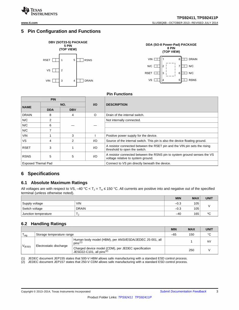
5 Pin Configuration and Functions
DBV (SOT23-5) PACKAGEDDA (SO-8 Power-Pad) PACKAGE5 PIN
8 PIN(TOP VIEW)(TOP VIEW)
Pin FunctionsPIN
NO. I/O DESCRIPTIONNAME
DDA DBVDRAIN 8 4 O Drain of the internal switch.N/C 2 Not internally connected.N/C 6 — —N/C 7VIN 1 3 I Positive power supply for the device.VS 4 2 I/O Source of the internal switch. This pin is also the device floating ground.
A resistor connected between the RSET pin and the VIN pin sets the risingRSET 3 1 I/O threshold to open the switch.A resistor connected between the RSNS pin to system ground senses the VSRSNS 5 5 I/O voltage relative to system ground.
Exposed Themal Pad Connect to VS pin directly beneath the device.
6 Specifications
6.1 Absolute Maximum RatingsAll voltages are with respect to VS, –40 °C < TJ = TA ≤ 150 °C. All currents are positive into and negative out of the specifiedterminal (unless otherwise noted).
MIN MAX UNITSupply voltage VIN –0.3 105
VSwitch voltage DRAIN –0.3 105Junction temperature TJ –40 165 ºC
6.2 Handling RatingsMIN MAX UNIT
Tstg Storage temperature range –65 150 °CHuman body model (HBM), per ANSI/ESDA/JEDEC JS-001, all 1 kVpins (1)
V(ESD) Electrostatic dischargeCharged device model (CDM), per JEDEC specification 250 VJESD22-C101, all pins (2)
(1) JEDEC document JEP155 states that 500-V HBM allows safe manufacturing with a standard ESD control process.(2) JEDEC document JEP157 states that 250-V CDM allows safe manufacturing with a standard ESD control process.
Copyright © 2013–2014, Texas Instruments Incorporated Submit Documentation Feedback 3
Product Folder Links: TPS92411 TPS92411P

TPS92411, TPS92411PSLUSBQ6B –OCTOBER 2013–REVISED JULY 2014 www.ti.com
6.3 Recommended Operating ConditionsOver operating free-air temperature range (unless otherwise noted)
MIN TYP MAX UNITTPS92411P 7.5 94
VIN Input voltage VTPS92411 7.5 100
TJ Operating junction temperature –40 25 150 °C
6.4 Thermal InformationTPS92411
THERMAL METRIC (1) DBV DDA UNIT5 PINS 8 PINS
θJA Junction-to-ambient thermal resistance (2) 209.8 58.6θJCtop Junction-to-case (top) thermal resistance (3) 125.2 72θJB Junction-to-board thermal resistance (4) 38 39.1
°C/WψJT Junction-to-top characterization parameter (5) 15.6 21.6ψJB Junction-to-board characterization parameter (6) 37.1 39.1θJCbot Junction-to-case (bottom) thermal resistance (7) N/A 15
(1) For more information about traditional and new thermal metrics, see the IC Package Thermal Metrics application report, SPRA953.(2) The junction-to-ambient thermal resistance under natural convection is obtained in a simulation on a JEDEC-standard, high-K board, as
specified in JESD51-7, in an environment described in JESD51-2a.(3) The junction-to-case (top) thermal resistance is obtained by simulating a cold plate test on the package top. No specified JEDEC-
standard test exists, but a close description can be found in the ANSI SEMI standard G30-88.(4) The junction-to-board thermal resistance is obtained by simulating in an environment with a ring cold plate fixture to control the PCB
temperature, as described in JESD51-8.(5) The junction-to-top characterization parameter, θJT, estimates the junction temperature of a device in a real system and is extracted
from the simulation data for obtaining θJA, using a procedure described in JESD51-2a (sections 6 and 7).(6) The junction-to-board characterization parameter, θJB, estimates the junction temperature of a device in a real system and is extracted
from the simulation data for obtaining θJA, using a procedure described in JESD51-2a (sections 6 and 7).(7) The junction-to-case (bottom) thermal resistance is obtained by simulating a cold plate test on the exposed (power) pad. No specific
JEDEC standard test exists, but a close description can be found in the ANSI SEMI standard G30-88.
6.5 Electrical CharacteristicsUnless otherwise specified –40 °C ≤ TJ = TA ≤ 150 °C, (VVIN – VVS) = 30 V, RRSET = RRSNS = Open, all voltages are withrespect to VS.
PARAMETER TEST CONDITIONS MIN TYP MAX UNITINPUT SUPPLY (VIN)
Rising threshold 95 100Input overvoltageVIN(ovp) TPS92411P Falling threshold 96 Vprotection
Hysteresis 4IQ Bias current 200 400 μAVIN(uvlo) Input undervoltage lockout Rising threshold 6.5 7 VVIN(hys) Input UVLO hysteresis 370 mVSWITCH CONTROL (RSNS, RSET)IRSNS RSNS threshold current –3.3 –4 –4.9 μAVRSNS_OS RSNS offset voltage 165 210 255 mVVRSET RSET threshold voltage 1.2 1.25 1.3 V
IRSNS = –20 μA, (VRSET – VVS) = 1.5 V –9.3 –10 –10.7IRSET RSET current IRSNS = –40 μA, (VRSET – VVS) = 1.5 V –19 –20 –21 μA
IRSNS = –100 μA, (VRSET – VVS) = 1.5 V –47.9 –50 –52.1SWITCH (DRAIN, VS)RDS(on) On-resistance IDRAIN = 100 mA, TJ = 25°C 1 2 2.5 Ω
4 Submit Documentation Feedback Copyright © 2013–2014, Texas Instruments Incorporated
Product Folder Links: TPS92411 TPS92411P

TPS92411, TPS92411Pwww.ti.com SLUSBQ6B –OCTOBER 2013–REVISED JULY 2014
Electrical Characteristics (continued)Unless otherwise specified –40 °C ≤ TJ = TA ≤ 150 °C, (VVIN – VVS) = 30 V, RRSET = RRSNS = Open, all voltages are withrespect to VS.
PARAMETER TEST CONDITIONS MIN TYP MAX UNIT(VDRAIN – VVS) falling 36 V to 4 V, 1dv/dt(ON) Switch ON slew rate ISW = 100 mA
V/μs(VDRAIN – VVS) = rising 4 V to 36 V, 0.5dv/dt(OFF) Switch OFF slew rate ISW = 100 mA
Copyright © 2013–2014, Texas Instruments Incorporated Submit Documentation Feedback 5
Product Folder Links: TPS92411 TPS92411P

0
1
2
3
4
5
−40 −25 −10 5 20 35 50 65 80 95 110 125 140 155Junction Temperature (°C)
Sw
itch
ON
Res
ista
nce
(Ω)
G004
100
120
140
160
180
200
−40 −25 −10 5 20 35 50 65 80 95 110 125 140 155Junction Temperature (°C)
Sup
ply
Cur
rent
(µA
)
G005
0
0.2
0.5
0.8
1
1.2
1.5
1.8
2
−40 −25 −10 5 20 35 50 65 80 95 110 125 140 155Junction Temperature (°C)
RS
ET
Thr
esho
ld (
V)
G002
−10
−8
−6
−4
−2
0
−40 −25 −10 5 20 35 50 65 80 95 110 125 140 155Junction Temperature (°C)
RS
NS
Thr
esho
ld C
urre
nt (
µA)
G003
0
2
4
6
8
10
−40 −25 −10 5 20 35 50 65 80 95 110 125 140 155Junction Temperature (°C)
VIN
− V
S U
VLO
Ris
ing
(V)
G000
0
2
4
6
8
10
−40 −25 −10 5 20 35 50 65 80 95 110 125 140 155Junction Temperature (°C)
VIN
− V
S U
VLO
Fal
ling
(V)
G001
TPS92411, TPS92411PSLUSBQ6B –OCTOBER 2013–REVISED JULY 2014 www.ti.com
6.6 Typical CharacteristicsUnless otherwise stated, –40 °C ≤ TA = TJ ≤ 150 °C, (VVIN – VVS) = 30 V, all voltages are with respect to VS.
Figure 1. UVLO vs. Temperature Figure 2. UVLO vs. Temperature
Figure 3. RSET Threshold vs. Temperature Figure 4. RSNS Threshold Current vs. Temperature
Figure 5. Switch On-Resistance (RDS(on)) vs. Temperature Figure 6. Input Voltage Quiescent Current vs. Temperature
6 Submit Documentation Feedback Copyright © 2013–2014, Texas Instruments Incorporated
Product Folder Links: TPS92411 TPS92411P

90
94
98
102
106
110
−40 −25 −10 5 20 35 50 65 80 95 110 125 140 155Junction Temperature (°C)
VIN
− V
S V
olta
ge (
V)
TPS92411P
G006
TPS92411, TPS92411Pwww.ti.com SLUSBQ6B –OCTOBER 2013–REVISED JULY 2014
Typical Characteristics (continued)Unless otherwise stated, –40 °C ≤ TA = TJ ≤ 150 °C, (VVIN – VVS) = 30 V, all voltages are with respect to VS.
Figure 7. (VVIN – VVS) Overvoltage Threshold vs. Temperature
Copyright © 2013–2014, Texas Instruments Incorporated Submit Documentation Feedback 7
Product Folder Links: TPS92411 TPS92411P

TPS92411
RSET
VIN
5 0
VDDBuffer
VIN UVLO6.5 V/6.13 V
+
Reference
UVLO
+±
VS
1.25 V
+±
VS
12 V
1x 1x
1x 2x 1x
+
+±
VS
RSNS
2 µA
VS
S Q
ROV
UVLO VCC
DRAIN
VS
2
VDDVCC
210 mV
Set dominant
TPS92411, TPS92411PSLUSBQ6B –OCTOBER 2013–REVISED JULY 2014 www.ti.com
7 Detailed Description
7.1 OverviewThe TPS92411 is an advanced, floating driver specifically designed for use with a linear regulator in low-poweroffline LED lighting applications. It integrates an on-board 100-V MOSFET switch to shunt LED current as theline transitions. As the line transitions through the cycle, the device monitors critical nodes for zero cross at whichtime the internal switch is either opened or shorted to steer the current through or away from the LED stack. TheTPS92411 does not directly control output power or LED current, it just directs current to the LED stack orbypasses the LED stack.
7.2 Functional Block Diagram
Figure 8. TPS92411 Block Diagram
8 Submit Documentation Feedback Copyright © 2013–2014, Texas Instruments Incorporated
Product Folder Links: TPS92411 TPS92411P

TPS92411P
RSET
VIN
VDDBuffer
VIN UVLO6.5 V/6.13 V
+
Reference
UVLO
+±
VS
1.25 V
+±
VS
12 V
1x 1x
1x 2x 1x
+
+±
VS
RSNS
2 µA
VS
S Q
R
3.95 0
50 N
VS
+
+±
VS
OV
UVLO VCC
OV
DRAIN
VS
1.25 V
2
VDDVCC
210 mV
Set dominant
5 0
TPS92411, TPS92411Pwww.ti.com SLUSBQ6B –OCTOBER 2013–REVISED JULY 2014
Functional Block Diagram (continued)
Figure 9. TPS92411P Block Diagram
7.3 Feature Description
7.3.1 Overvoltage Protection (OVP)Overvoltage protection (OVP) in the TPS92411P version protects the device as well as the LEDs and storagecapacitor. The OVP is set at approximately 100 V (VVIN – VVS) and closes the internal switch when the thresholdvoltage is reached. For this reason LED stack voltages of 94 V or less are recommended. Higher voltages canbe used with the TPS92411 version but tolerances must be considered to ensure that the 105 V absolutemaximum rating is not exceeded.
7.3.2 Input Undervoltage Lockout (UVLO)The TPS92411 includes input UVLO. The UVLO prevents the device from operation until the VIN pin voltage withrespect to VS exceeds 6.5 V and ensures the device behaves properly when enabled.
7.3.3 LED CapacitorA capacitor is required across each LED stack to provide current to the LEDs during the switch ON time. Refer tothe available calculator software (SLVC516 for 120-V applications or SLVC517 for 230-V applications) forcalculating the minimum value required for any particular application. The software calculates the minimum valuerequired for a particular application, but best performance is acheived by using as much capacitance as possiblegiven size and cost constraints. These design tools also calculate a minimum value for any given current ripplepercent or flicker index desired for the particular application.
7.3.4 Blocking DiodeA blocking diode is required between the drain of the switch (DRAIN) and the anode of the LED stack. Thisprevents the LED capacitor from discharging through the switch during the switch ON time instead allowing it todischarge through the LED stack. This diode should be rated for 200 V reverse voltage and capable of forwardcurrents as high as the average linear regulator current setting.
Copyright © 2013–2014, Texas Instruments Incorporated Submit Documentation Feedback 9
Product Folder Links: TPS92411 TPS92411P

TPS92411, TPS92411PSLUSBQ6B –OCTOBER 2013–REVISED JULY 2014 www.ti.com
7.4 Device Functional ModesThe TPS92411P has 4 functional modes while the TPS92411 has 3:
7.4.1 Input UVLOAs described in the previous section the device and internal switch will remain off until VIN is 6.5V or greater withrespect to VS.
7.4.2 Operating with Internal Switch ONAfter the device crosses the UVLO threshold the internal switch will turn on and remain on until the voltage at theVIN pin exceeds the threshold voltage set by the RSET resistor.
7.4.3 Operating with Internal Switch OFFWhen the RSET threshold voltage is exceeded on the VIN pin the internal switch will turn off forcing all thecurrent to flow through the LEDs and charge the LED capacitor. The switch will remain off until the VS pin dropsbelow the threshold voltage set by RSNS or an overvoltage event occurs (TPS92411P only).
7.4.4 Overvoltage Operation (TPS92411P)If an LED fails open or a string voltage exceeding the OVP level is used the device will enter OVP operation. Theinternal switch will close and remain closed until the VIN voltage with respect to the VS pin drops low enough toengage normal operation again.
10 Submit Documentation Feedback Copyright © 2013–2014, Texas Instruments Incorporated
Product Folder Links: TPS92411 TPS92411P

TPS92411, TPS92411Pwww.ti.com SLUSBQ6B –OCTOBER 2013–REVISED JULY 2014
8 Application and Implementation
8.1 Application InformationThe TPS92411 is an advanced, floating driver specifically designed for use with a linear regulator in low-poweroffline LED lighting applications. It integrates an on-board 100-V MOSFET switch to shunt LED current as theline transitions. As the line transitions through the cycle, the device monitors critical nodes for zero cross at whichtime the internal switch is either opened or shorted to steer the current through or away from the LED stack. Usethe following design procedure to select components for the TPS92411. The following calculators may also beused to select components for the TPS92411:• SLVC579 for 120-V applications using the TPS92410• SLVC580 for 230-V applications using the TPS92410• SLVC516 for 120-V applications using a discrete linear regulator• SLVC517 for 230-V applications using a discrete linear regulator
PSpice and TINA-TI models are also available. The following are typical applications using the TPS92411 forboth 120-V and 230-V applications using a discrete linear regulator.
Copyright © 2013–2014, Texas Instruments Incorporated Submit Documentation Feedback 11
Product Folder Links: TPS92411 TPS92411P

VIN
RSET
TPS92411
RSNS
DRAIN
VS33 µF100 V
VIN
RSET
TPS92411
RSNS
DRAIN
VS
VIN
RSET
TPS92411
RSNS
DRAIN
VS
0.01 µF
RCS24
± +
120 VRMS
22
0.22 µF250 V
442
0.1 µF250 V
1.82 0
1.65 0
1.43 0
1 0
1 0
1 0
200 V
200 V
68 µF50 V
200 V
120 µF25 V
Q1600 V2 A
1 N
12 V
499 N90.9 N
5 N
Q2200 mW
200 N
91 V
0.22 µF
2 0
44.2 N
0.1 µF
732 N
TPS92411, TPS92411PSLUSBQ6B –OCTOBER 2013–REVISED JULY 2014 www.ti.com
8.2 Typical Application
8.2.1 120-VAC, Phase Dimmable 11.5-W Input with Discrete Linear Regulator
Figure 10. 120-VAC, Phase Dimmable 11.5-W Input with Discrete Linear Regulator
8.2.1.1 Design RequirementsFor the 120-V application shown in Figure 10 the highest efficiency is obtained by using a high-voltage total LEDstack to reduce losses in the linear regulator FET. The best current sharing efficiency between stacks can beachieved by using the lowest voltage stack at the bottom and making each stack voltage above 2 times thevoltage of the stack below it. In this example 20-V LEDs are used. This effectively gives the lowest stack a totalof 20 V, the middle stack a total of 40 V, and the upper stack a total of 80 V. The RSNS resistor is used to set a
12 Submit Documentation Feedback Copyright © 2013–2014, Texas Instruments Incorporated
Product Folder Links: TPS92411 TPS92411P

( )- ´ ´=
+
LED SNS
RSET
VS
V 1.24 V 2 RR
V 0.21V
+
=SNS
SNS
RSNS
V 0.21VR
I
TPS92411, TPS92411Pwww.ti.com SLUSBQ6B –OCTOBER 2013–REVISED JULY 2014
Typical Application (continued)low voltage point so that when the VS pin voltage falls below this threshold (either from the AC line falling or ahigher voltage stack switch above it turning OFF) the TPS92411 switch turns ON and bypasses the LEDs. Duringthe ON-time, the LEDs are supplied current from the capacitor. The RSET voltage is used to set a threshold todetect when the input voltage crosses this threshold it turns OFF the switch and allows the LEDs to conductcurrent from the line and charge the bypass capacitor.
8.2.1.2 Detailed Design Procedure• Set VRSNS for all three TPS92411 devices at 4 V• Set VRSET for the bottom stack at 26 V (20 V stack plus 6 V headroom)• Set VRSET for the middle stack at 46 V (40 V stack plus 6 V headroom)• Set VRSET for the top stack at 86 V (80 V stack plus 6 V headroom)
Switching order as the rectified AC line voltage increases is shown in Table 1. Figure 11 illustrates when eachswitch turns ON or OFF.
8.2.1.2.1 Setting the Switching Thresholds (RSNS, RSET)
The TPS92411 features two threshold settings to allow for proper LED control. The first setting determines whenthe internal switch turns off and allows current to charge the capacitor and flow through the LEDs. The secondsetting determines when the switch turns on to shunt the LEDs and allow the capacitor to supply current. Thelower switch turn-on threshold (VSNS) should be set first using a resistor (RRSNS) from the RSNS pin to systemground. For best efficiency set this threshold between 4 V and 6 V. Then the upper switch turn-off threshold (VVS)can be set using a resistor (RRSET) from the RSET pin to the VIN pin. Set this threshold approximately 6 V to 10V above the LED stack voltage (VLED). The RSET threshold should be greater than the LED stack voltage plusthe value of the RSNS threshold to prevent errant switching. These thresholds can be set with resistancecalculated using Equation 1 and Equation 2.
(1)
(2)
Table 1. Switching Order on Rising Edge of Rectified 120-VAC (1) (2)
STACKTOP 80-V MIDDLE 40-V BOTTOM 20-V
0 0 00 0 10 1 00 1 11 0 01 0 11 1 01 1 1
(1) 0 denotes switch ON and LEDs bypassed and supplied by the capacitor.(2) 1 denotes switch OFF and LEDs conducting from the line, capacitor charging up.
Copyright © 2013–2014, Texas Instruments Incorporated Submit Documentation Feedback 13
Product Folder Links: TPS92411 TPS92411P

0.90
0.91
0.92
0.93
0.94
0.95
0.96
0.97
0.98
0.99
1.00
190 200 210 220 230 240 250 260
Pow
er F
acto
r
Input Voltage (VAC) C001
´
=RMS RMS
CS
IN
120 V 2.3VR
P
Time
Rec
tifie
d A
C (
V)
26
46
66
86
106
126
000001
010
011
100
101
110
111146 110101
100
011
010
001
000 24
44
64
84
104
124
144
Voltage trip points do not include diode drops
TPS92411, TPS92411PSLUSBQ6B –OCTOBER 2013–REVISED JULY 2014 www.ti.com
Figure 11. Switching Order on Rectified 120-VAC Waveform
The linear regulator in Figure 11 generates a current sense RMS voltage of approximately 2.3 V. The linearregulator RMS current is equal to the input current drawn from the AC line. For example, for a 11.5-W inputpower system the input current should be approximately 0.095 A and a 24-Ω resistor should be chosen for RCS.Other input power levels (PIN) can be obtained using Equation 3.
(3)
8.2.1.3 Application Curve
Figure 12. Power Factor vs. Input Voltage
14 Submit Documentation Feedback Copyright © 2013–2014, Texas Instruments Incorporated
Product Folder Links: TPS92411 TPS92411P

VIN
RSET
TPS92411
RSNS
DRAIN
VS
0.1 µF100 V
VIN
RSET
TPS92411
RSNS
DRAIN
VS
VIN
RSET
TPS92411
RSNS
DRAIN
VS
0.022 µF
RCS34.8
± +
230 VRMS
68
0.15 µF400 V
550
0.033 µF400 V
2.8 0
2.67 0
2.37 0
1.5 0
1.5 0
1.5 0
200 V
200 V
47 µF100 V
200 V
100 µF50 V
Q1600 V2 A
10 N
12 V
1 0100 N
4.99 N
Q2200 mW
68 V
0.22 µF
442 N
0.1 µF
100 N
249 N
12 V 12 V
22 µF200 V
1 0
10 N
680 pF1 N Q3200 VVGS = 4 V
TPS92411, TPS92411Pwww.ti.com SLUSBQ6B –OCTOBER 2013–REVISED JULY 2014
8.2.2 230-VAC, Phase Dimmable 16-W Input with Discrete Linear Regulator
Figure 13. 230-VAC, Phase Dimmable 16-W Input with Discrete Linear Regulator
8.2.2.1 Design RequirementsIn the 230-V application shown in Figure 13, the highest efficiency can be obtained by using a high-voltage totalLED stack to reduce losses in the linear regulator FET. The best current sharing between stacks can beachieved by using the lowest voltage stack at the bottom and making each stack voltage above that two timesthat of the stack below it (as in described in the 120-V application). In this example, very good results can beobtained by setting the lowest stack at 40 V, the middle stack at 80 V, and adding a high-voltage cascode FETwith the top stack and using 160 V. Use the RSNS pin to set a low voltage point so that when the VS pin of the
Copyright © 2013–2014, Texas Instruments Incorporated Submit Documentation Feedback 15
Product Folder Links: TPS92411 TPS92411P

´
=RMS RMS
CS
IN
230 V 2.44VR
P
Time
Rec
tifie
d A
C (
V)
49
89
129
169
209
249
000001
010
011
100
101
110
111289 110101
100
011
010
001
000 46
86
126
166
206
246
286
Voltage trip points do not include diode drops
TPS92411, TPS92411PSLUSBQ6B –OCTOBER 2013–REVISED JULY 2014 www.ti.com
device falls below this threshold (either from the AC line falling or a higher voltage stack switch above it turningOFF) the TPS92411 switch turns ON and bypasses the LEDs. During the ON-time, the capacitor supplies currentto the LEDs. The RSET voltage threshold for a 230-V application is generally set to approximately 8 V to 12 Vabove the LED stack voltage connected across the TPS92411 (for an RSNS voltage of 6 V). This threshold ishigher than in the typical 120-V application to allow more headroom.
8.2.2.2 Detailed Design Procedure• Set VRSNS for all three TPS92411 devices at 6 V• Set VRSET for the bottom stack at 49 V (40 V stack plus 9 V headroom)• Set VRSET for the middle stack at 89 V (80 V stack plus 9 V headroom)• Set VRSET for the top stack at 169 V (160 V stack plus 9 V headroom)
Switching order as the rectified AC line voltage increases is shown in Table 2. Figure 14 illustrates when eachswitch turns ON or OFF.
Table 2. Switching Order on Rising Edge of the Rectified 230-VACWaveform (1) (2)
STACKTOP 160-V MIDDLE 80-V BOTTOM 40-V
0 0 00 0 10 1 00 1 11 0 01 0 11 1 01 1 1
(1) 0 denotes switch ON and LEDs bypassed and supplied by the capacitor.(2) 1 denotes switch OFF and LEDs conducting from the line, capacitor charging up.
Figure 14. Switching Order on Rising Edge of the Rectified 230-VAC Waveform
The linear regulator in Figure 14 generates a current sense RMS voltage of 2.44 V. The linear regulator RMScurrent is equal to the input current drawn from the AC line. For example, for a 16-W input power system theinput current should be approximately 0.07 A and a 34.8-Ω resistor should be chosen for RCS. Other input powerlevels (PIN) can be calculated using Equation 4.
(4)
16 Submit Documentation Feedback Copyright © 2013–2014, Texas Instruments Incorporated
Product Folder Links: TPS92411 TPS92411P

0.90
0.91
0.92
0.93
0.94
0.95
0.96
0.97
0.98
0.99
1.00
190 200 210 220 230 240 250 260
Pow
er F
acto
r
Input Voltage (VAC) C001
TPS92411, TPS92411Pwww.ti.com SLUSBQ6B –OCTOBER 2013–REVISED JULY 2014
8.2.2.3 Application Curve
Figure 15. Power Factor Input Voltage
Copyright © 2013–2014, Texas Instruments Incorporated Submit Documentation Feedback 17
Product Folder Links: TPS92411 TPS92411P

LED-/VS
1-VIN
3-RSET
4-VS
7-NC
8-DRAIN
5-RSNS
6-NC
2-NC
LED+
To rectified AC or VS of
TPS92411 above
System
GND
LED-/VS
1-RSET
3-VIN
5-RSNS
4-DRAIN
2-VS
LED+To rectified AC or VS of
TPS92411 above
System
GND
TPS92411, TPS92411PSLUSBQ6B –OCTOBER 2013–REVISED JULY 2014 www.ti.com
9 Power Supply Recommendations
For testing purposes any benchtop adjustable AC power supply with a power rating higher than what is requiredby the circuit is suitable. An example would be an Hewlett Packard 6811B or equivalent. An isolated supply isrecommended for safety purposes.
10 Layout
10.1 Layout GuidelinesThe TPS92411 allows for a simple layout, however some considerations should be taken. The RSET resistorshould be connected directly between the RSET pin and VIN pin as close to the device as possible. The tracebetween the resistor and the RSET pin should be as short as possible. The trace from the RSNS pin to theRSNS resistor should also be as short as possible to minimize parasitic capacitances. The blocking diode shouldbe placed between the DRAIN pin and the VIN pin and also located close to the device. Placement of the LEDcapacitor may depend on the physical design of the application, however it should be placed as close to theTPS92411 as the design allows to minimize parasitic inductances.
10.2 Layout Example
Figure 16. Recommended Component Placement (DBV)
Figure 17. Recommended Component Placement (DDA)
18 Submit Documentation Feedback Copyright © 2013–2014, Texas Instruments Incorporated
Product Folder Links: TPS92411 TPS92411P

TPS92411, TPS92411Pwww.ti.com SLUSBQ6B –OCTOBER 2013–REVISED JULY 2014
11 Device and Documentation Support
11.1 Related LinksThe table below lists quick access links. Categories include technical documents, support and communityresources, tools and software, and quick access to sample or buy.
Table 3. Related LinksTECHNICAL TOOLS & SUPPORT &PARTS PRODUCT FOLDER SAMPLE & BUY DOCUMENTS SOFTWARE COMMUNITY
TPS92411 Click here Click here Click here Click here Click hereTPS92411P Click here Click here Click here Click here Click here
11.2 TrademarksAll trademarks are the property of their respective owners.
11.3 Electrostatic Discharge CautionThese devices have limited built-in ESD protection. The leads should be shorted together or the device placed in conductive foamduring storage or handling to prevent electrostatic damage to the MOS gates.
11.4 GlossarySLYZ022 — TI Glossary.
This glossary lists and explains terms, acronyms, and definitions.
12 Mechanical, Packaging, and Orderable InformationThe following pages include mechanical, packaging, and orderable information. This information is the mostcurrent data available for the designated devices. This data is subject to change without notice and revision ofthis document. For browser-based versions of this data sheet, refer to the left-hand navigation.
Copyright © 2013–2014, Texas Instruments Incorporated Submit Documentation Feedback 19
Product Folder Links: TPS92411 TPS92411P

PACKAGE OPTION ADDENDUM
www.ti.com 17-May-2014
Addendum-Page 1
PACKAGING INFORMATION
Orderable Device Status(1)
Package Type PackageDrawing
Pins PackageQty
Eco Plan(2)
Lead/Ball Finish(6)
MSL Peak Temp(3)
Op Temp (°C) Device Marking(4/5)
Samples
TPS92411DBVR ACTIVE SOT-23 DBV 5 3000 Green (RoHS& no Sb/Br)
CU NIPDAU Level-1-260C-UNLIM -40 to 150 PB9Q
TPS92411DBVT ACTIVE SOT-23 DBV 5 250 Green (RoHS& no Sb/Br)
CU NIPDAU Level-1-260C-UNLIM -40 to 150 PB9Q
TPS92411DDA ACTIVE SO PowerPAD DDA 8 75 Green (RoHS& no Sb/Br)
CU NIPDAUAG Level-2-260C-1 YEAR -40 to 150 92411
TPS92411DDAR ACTIVE SO PowerPAD DDA 8 2500 Green (RoHS& no Sb/Br)
CU NIPDAUAG Level-2-260C-1 YEAR -40 to 150 92411
TPS92411PDBVR ACTIVE SOT-23 DBV 5 3000 Green (RoHS& no Sb/Br)
CU NIPDAU Level-1-260C-UNLIM -40 to 150 PB8Q
TPS92411PDBVT ACTIVE SOT-23 DBV 5 250 Green (RoHS& no Sb/Br)
CU NIPDAU Level-1-260C-UNLIM -40 to 150 PB8Q
TPS92411PDDA ACTIVE SO PowerPAD DDA 8 75 Green (RoHS& no Sb/Br)
CU NIPDAUAG Level-2-260C-1 YEAR -40 to 150 92411P
TPS92411PDDAR ACTIVE SO PowerPAD DDA 8 2500 Green (RoHS& no Sb/Br)
CU NIPDAUAG Level-2-260C-1 YEAR -40 to 150 92411P
(1) The marketing status values are defined as follows:ACTIVE: Product device recommended for new designs.LIFEBUY: TI has announced that the device will be discontinued, and a lifetime-buy period is in effect.NRND: Not recommended for new designs. Device is in production to support existing customers, but TI does not recommend using this part in a new design.PREVIEW: Device has been announced but is not in production. Samples may or may not be available.OBSOLETE: TI has discontinued the production of the device.
(2) Eco Plan - The planned eco-friendly classification: Pb-Free (RoHS), Pb-Free (RoHS Exempt), or Green (RoHS & no Sb/Br) - please check http://www.ti.com/productcontent for the latest availabilityinformation and additional product content details.TBD: The Pb-Free/Green conversion plan has not been defined.Pb-Free (RoHS): TI's terms "Lead-Free" or "Pb-Free" mean semiconductor products that are compatible with the current RoHS requirements for all 6 substances, including the requirement thatlead not exceed 0.1% by weight in homogeneous materials. Where designed to be soldered at high temperatures, TI Pb-Free products are suitable for use in specified lead-free processes.Pb-Free (RoHS Exempt): This component has a RoHS exemption for either 1) lead-based flip-chip solder bumps used between the die and package, or 2) lead-based die adhesive used betweenthe die and leadframe. The component is otherwise considered Pb-Free (RoHS compatible) as defined above.Green (RoHS & no Sb/Br): TI defines "Green" to mean Pb-Free (RoHS compatible), and free of Bromine (Br) and Antimony (Sb) based flame retardants (Br or Sb do not exceed 0.1% by weightin homogeneous material)
(3) MSL, Peak Temp. - The Moisture Sensitivity Level rating according to the JEDEC industry standard classifications, and peak solder temperature.

PACKAGE OPTION ADDENDUM
www.ti.com 17-May-2014
Addendum-Page 2
(4) There may be additional marking, which relates to the logo, the lot trace code information, or the environmental category on the device.
(5) Multiple Device Markings will be inside parentheses. Only one Device Marking contained in parentheses and separated by a "~" will appear on a device. If a line is indented then it is a continuationof the previous line and the two combined represent the entire Device Marking for that device.
(6) Lead/Ball Finish - Orderable Devices may have multiple material finish options. Finish options are separated by a vertical ruled line. Lead/Ball Finish values may wrap to two lines if the finishvalue exceeds the maximum column width.
Important Information and Disclaimer:The information provided on this page represents TI's knowledge and belief as of the date that it is provided. TI bases its knowledge and belief on informationprovided by third parties, and makes no representation or warranty as to the accuracy of such information. Efforts are underway to better integrate information from third parties. TI has taken andcontinues to take reasonable steps to provide representative and accurate information but may not have conducted destructive testing or chemical analysis on incoming materials and chemicals.TI and TI suppliers consider certain information to be proprietary, and thus CAS numbers and other limited information may not be available for release.
In no event shall TI's liability arising out of such information exceed the total purchase price of the TI part(s) at issue in this document sold by TI to Customer on an annual basis.

TAPE AND REEL INFORMATION
*All dimensions are nominal
Device PackageType
PackageDrawing
Pins SPQ ReelDiameter
(mm)
ReelWidth
W1 (mm)
A0(mm)
B0(mm)
K0(mm)
P1(mm)
W(mm)
Pin1Quadrant
TPS92411DBVR SOT-23 DBV 5 3000 178.0 9.0 3.23 3.17 1.37 4.0 8.0 Q3
TPS92411DBVT SOT-23 DBV 5 250 178.0 9.0 3.23 3.17 1.37 4.0 8.0 Q3
TPS92411DDAR SOPower PAD
DDA 8 2500 330.0 12.8 6.4 5.2 2.1 8.0 12.0 Q1
TPS92411PDBVR SOT-23 DBV 5 3000 178.0 9.0 3.23 3.17 1.37 4.0 8.0 Q3
TPS92411PDBVT SOT-23 DBV 5 250 178.0 9.0 3.23 3.17 1.37 4.0 8.0 Q3
TPS92411PDDAR SOPower PAD
DDA 8 2500 330.0 12.8 6.4 5.2 2.1 8.0 12.0 Q1
PACKAGE MATERIALS INFORMATION
www.ti.com 7-May-2015
Pack Materials-Page 1
*All dimensions are nominal
Device Package Type Package Drawing Pins SPQ Length (mm) Width (mm) Height (mm)
TPS92411DBVR SOT-23 DBV 5 3000 180.0 180.0 18.0
TPS92411DBVT SOT-23 DBV 5 250 180.0 180.0 18.0
TPS92411DDAR SO PowerPAD DDA 8 2500 366.0 364.0 50.0
TPS92411PDBVR SOT-23 DBV 5 3000 180.0 180.0 18.0
TPS92411PDBVT SOT-23 DBV 5 250 180.0 180.0 18.0
TPS92411PDDAR SO PowerPAD DDA 8 2500 366.0 364.0 50.0
PACKAGE MATERIALS INFORMATION
www.ti.com 7-May-2015
Pack Materials-Page 2


www.ti.com
PACKAGE OUTLINE
C
TYP0.220.08
0.25
3.02.6
2X 0.95
1.9
1.45 MAX
TYP0.150.00
5X 0.50.3
TYP0.60.3
TYP80
1.9
A
3.052.75
B1.751.45
(1.1)
SOT-23 - 1.45 mm max heightDBV0005ASMALL OUTLINE TRANSISTOR
4214839/C 04/2017
NOTES: 1. All linear dimensions are in millimeters. Any dimensions in parenthesis are for reference only. Dimensioning and tolerancing per ASME Y14.5M.2. This drawing is subject to change without notice.3. Refernce JEDEC MO-178.
0.2 C A B
1
34
5
2
INDEX AREAPIN 1
GAGE PLANE
SEATING PLANE
0.1 C
SCALE 4.000

www.ti.com
EXAMPLE BOARD LAYOUT
0.07 MAXARROUND
0.07 MINARROUND
5X (1.1)
5X (0.6)
(2.6)
(1.9)
2X (0.95)
(R0.05) TYP
4214839/C 04/2017
SOT-23 - 1.45 mm max heightDBV0005ASMALL OUTLINE TRANSISTOR
NOTES: (continued) 4. Publication IPC-7351 may have alternate designs. 5. Solder mask tolerances between and around signal pads can vary based on board fabrication site.
SYMM
LAND PATTERN EXAMPLEEXPOSED METAL SHOWN
SCALE:15X
PKG
1
3 4
5
2
SOLDER MASKOPENINGMETAL UNDER
SOLDER MASK
SOLDER MASKDEFINED
EXPOSED METAL
METALSOLDER MASKOPENING
NON SOLDER MASKDEFINED
(PREFERRED)
SOLDER MASK DETAILS
EXPOSED METAL

www.ti.com
EXAMPLE STENCIL DESIGN
(2.6)
(1.9)
2X(0.95)
5X (1.1)
5X (0.6)
(R0.05) TYP
SOT-23 - 1.45 mm max heightDBV0005ASMALL OUTLINE TRANSISTOR
4214839/C 04/2017
NOTES: (continued) 6. Laser cutting apertures with trapezoidal walls and rounded corners may offer better paste release. IPC-7525 may have alternate design recommendations. 7. Board assembly site may have different recommendations for stencil design.
SOLDER PASTE EXAMPLEBASED ON 0.125 mm THICK STENCIL
SCALE:15X
SYMM
PKG
1
3 4
5
2

www.ti.com
PACKAGE OUTLINE
C
TYP0.220.08
0.25
3.02.6
2X 0.95
1.9
1.45 MAX
TYP0.150.00
5X 0.50.3
TYP0.60.3
TYP80
1.9
A
3.052.75
B1.751.45
(1.1)
SOT-23 - 1.45 mm max heightDBV0005ASMALL OUTLINE TRANSISTOR
4214839/C 04/2017
NOTES: 1. All linear dimensions are in millimeters. Any dimensions in parenthesis are for reference only. Dimensioning and tolerancing per ASME Y14.5M.2. This drawing is subject to change without notice.3. Refernce JEDEC MO-178.
0.2 C A B
1
34
5
2
INDEX AREAPIN 1
GAGE PLANE
SEATING PLANE
0.1 C
SCALE 4.000

www.ti.com
EXAMPLE BOARD LAYOUT
0.07 MAXARROUND
0.07 MINARROUND
5X (1.1)
5X (0.6)
(2.6)
(1.9)
2X (0.95)
(R0.05) TYP
4214839/C 04/2017
SOT-23 - 1.45 mm max heightDBV0005ASMALL OUTLINE TRANSISTOR
NOTES: (continued) 4. Publication IPC-7351 may have alternate designs. 5. Solder mask tolerances between and around signal pads can vary based on board fabrication site.
SYMM
LAND PATTERN EXAMPLEEXPOSED METAL SHOWN
SCALE:15X
PKG
1
3 4
5
2
SOLDER MASKOPENINGMETAL UNDER
SOLDER MASK
SOLDER MASKDEFINED
EXPOSED METAL
METALSOLDER MASKOPENING
NON SOLDER MASKDEFINED
(PREFERRED)
SOLDER MASK DETAILS
EXPOSED METAL

www.ti.com
EXAMPLE STENCIL DESIGN
(2.6)
(1.9)
2X(0.95)
5X (1.1)
5X (0.6)
(R0.05) TYP
SOT-23 - 1.45 mm max heightDBV0005ASMALL OUTLINE TRANSISTOR
4214839/C 04/2017
NOTES: (continued) 6. Laser cutting apertures with trapezoidal walls and rounded corners may offer better paste release. IPC-7525 may have alternate design recommendations. 7. Board assembly site may have different recommendations for stencil design.
SOLDER PASTE EXAMPLEBASED ON 0.125 mm THICK STENCIL
SCALE:15X
SYMM
PKG
1
3 4
5
2

GENERIC PACKAGE VIEW
Images above are just a representation of the package family, actual package may vary.Refer to the product data sheet for package details.
DDA 8 PowerPAD TM SOIC - 1.7 mm max heightPLASTIC SMALL OUTLINE
4202561/G


IMPORTANT NOTICE
Texas Instruments Incorporated (TI) reserves the right to make corrections, enhancements, improvements and other changes to itssemiconductor products and services per JESD46, latest issue, and to discontinue any product or service per JESD48, latest issue. Buyersshould obtain the latest relevant information before placing orders and should verify that such information is current and complete.TI’s published terms of sale for semiconductor products (http://www.ti.com/sc/docs/stdterms.htm) apply to the sale of packaged integratedcircuit products that TI has qualified and released to market. Additional terms may apply to the use or sale of other types of TI products andservices.Reproduction of significant portions of TI information in TI data sheets is permissible only if reproduction is without alteration and isaccompanied by all associated warranties, conditions, limitations, and notices. TI is not responsible or liable for such reproduceddocumentation. Information of third parties may be subject to additional restrictions. Resale of TI products or services with statementsdifferent from or beyond the parameters stated by TI for that product or service voids all express and any implied warranties for theassociated TI product or service and is an unfair and deceptive business practice. TI is not responsible or liable for any such statements.Buyers and others who are developing systems that incorporate TI products (collectively, “Designers”) understand and agree that Designersremain responsible for using their independent analysis, evaluation and judgment in designing their applications and that Designers havefull and exclusive responsibility to assure the safety of Designers' applications and compliance of their applications (and of all TI productsused in or for Designers’ applications) with all applicable regulations, laws and other applicable requirements. Designer represents that, withrespect to their applications, Designer has all the necessary expertise to create and implement safeguards that (1) anticipate dangerousconsequences of failures, (2) monitor failures and their consequences, and (3) lessen the likelihood of failures that might cause harm andtake appropriate actions. Designer agrees that prior to using or distributing any applications that include TI products, Designer willthoroughly test such applications and the functionality of such TI products as used in such applications.TI’s provision of technical, application or other design advice, quality characterization, reliability data or other services or information,including, but not limited to, reference designs and materials relating to evaluation modules, (collectively, “TI Resources”) are intended toassist designers who are developing applications that incorporate TI products; by downloading, accessing or using TI Resources in anyway, Designer (individually or, if Designer is acting on behalf of a company, Designer’s company) agrees to use any particular TI Resourcesolely for this purpose and subject to the terms of this Notice.TI’s provision of TI Resources does not expand or otherwise alter TI’s applicable published warranties or warranty disclaimers for TIproducts, and no additional obligations or liabilities arise from TI providing such TI Resources. TI reserves the right to make corrections,enhancements, improvements and other changes to its TI Resources. TI has not conducted any testing other than that specificallydescribed in the published documentation for a particular TI Resource.Designer is authorized to use, copy and modify any individual TI Resource only in connection with the development of applications thatinclude the TI product(s) identified in such TI Resource. NO OTHER LICENSE, EXPRESS OR IMPLIED, BY ESTOPPEL OR OTHERWISETO ANY OTHER TI INTELLECTUAL PROPERTY RIGHT, AND NO LICENSE TO ANY TECHNOLOGY OR INTELLECTUAL PROPERTYRIGHT OF TI OR ANY THIRD PARTY IS GRANTED HEREIN, including but not limited to any patent right, copyright, mask work right, orother intellectual property right relating to any combination, machine, or process in which TI products or services are used. Informationregarding or referencing third-party products or services does not constitute a license to use such products or services, or a warranty orendorsement thereof. Use of TI Resources may require a license from a third party under the patents or other intellectual property of thethird party, or a license from TI under the patents or other intellectual property of TI.TI RESOURCES ARE PROVIDED “AS IS” AND WITH ALL FAULTS. TI DISCLAIMS ALL OTHER WARRANTIES ORREPRESENTATIONS, EXPRESS OR IMPLIED, REGARDING RESOURCES OR USE THEREOF, INCLUDING BUT NOT LIMITED TOACCURACY OR COMPLETENESS, TITLE, ANY EPIDEMIC FAILURE WARRANTY AND ANY IMPLIED WARRANTIES OFMERCHANTABILITY, FITNESS FOR A PARTICULAR PURPOSE, AND NON-INFRINGEMENT OF ANY THIRD PARTY INTELLECTUALPROPERTY RIGHTS. TI SHALL NOT BE LIABLE FOR AND SHALL NOT DEFEND OR INDEMNIFY DESIGNER AGAINST ANY CLAIM,INCLUDING BUT NOT LIMITED TO ANY INFRINGEMENT CLAIM THAT RELATES TO OR IS BASED ON ANY COMBINATION OFPRODUCTS EVEN IF DESCRIBED IN TI RESOURCES OR OTHERWISE. IN NO EVENT SHALL TI BE LIABLE FOR ANY ACTUAL,DIRECT, SPECIAL, COLLATERAL, INDIRECT, PUNITIVE, INCIDENTAL, CONSEQUENTIAL OR EXEMPLARY DAMAGES INCONNECTION WITH OR ARISING OUT OF TI RESOURCES OR USE THEREOF, AND REGARDLESS OF WHETHER TI HAS BEENADVISED OF THE POSSIBILITY OF SUCH DAMAGES.Unless TI has explicitly designated an individual product as meeting the requirements of a particular industry standard (e.g., ISO/TS 16949and ISO 26262), TI is not responsible for any failure to meet such industry standard requirements.Where TI specifically promotes products as facilitating functional safety or as compliant with industry functional safety standards, suchproducts are intended to help enable customers to design and create their own applications that meet applicable functional safety standardsand requirements. Using products in an application does not by itself establish any safety features in the application. Designers mustensure compliance with safety-related requirements and standards applicable to their applications. Designer may not use any TI products inlife-critical medical equipment unless authorized officers of the parties have executed a special contract specifically governing such use.Life-critical medical equipment is medical equipment where failure of such equipment would cause serious bodily injury or death (e.g., lifesupport, pacemakers, defibrillators, heart pumps, neurostimulators, and implantables). Such equipment includes, without limitation, allmedical devices identified by the U.S. Food and Drug Administration as Class III devices and equivalent classifications outside the U.S.TI may expressly designate certain products as completing a particular qualification (e.g., Q100, Military Grade, or Enhanced Product).Designers agree that it has the necessary expertise to select the product with the appropriate qualification designation for their applicationsand that proper product selection is at Designers’ own risk. Designers are solely responsible for compliance with all legal and regulatoryrequirements in connection with such selection.Designer will fully indemnify TI and its representatives against any damages, costs, losses, and/or liabilities arising out of Designer’s non-compliance with the terms and provisions of this Notice.
Mailing Address: Texas Instruments, Post Office Box 655303, Dallas, Texas 75265Copyright © 2018, Texas Instruments Incorporated