for use with universal socket 370 -...
TRANSCRIPT

h
Intel® 810E2 Chipset Platform Design Guide
For Use With Universal Socket 370 August 2002
Document Number: 298303-002
R
R
2 Design Guide
INFORMATION IN THIS DOCUMENT IS PROVIDED IN CONNECTION WITH INTEL® PRODUCTS. NO LICENSE, EXPRESS OR IMPLIED, BY ESTOPPEL OR OTHERWISE, TO ANY INTELLECTUAL PROPERTY RIGHTS IS GRANTED BY THIS DOCUMENT. EXCEPT AS PROVIDED IN INTELS TERMS AND CONDITIONS OF SALE FOR SUCH PRODUCTS, INTEL ASSUMES NO LIABILITY WHATSOEVER, AND INTEL DISCLAIMS ANY EXPRESS OR IMPLIED WARRANTY, RELATING TO SALE AND/OR USE OF INTEL PRODUCTS INCLUDING LIABILITY OR WARRANTIES RELATING TO FITNESS FOR A PARTICULAR PURPOSE, MERCHANTABILITY, OR INFRINGEMENT OF ANY PATENT, COPYRIGHT OR OTHER INTELLECTUAL PROPERTY RIGHT. Intel products are not intended for use in medical, life saving, or life sustaining applications.
Intel may make changes to specifications and product descriptions at any time, without notice.
Designers must not rely on the absence or characteristics of any features or instructions marked "reserved" or "undefined." Intel reserves these for future definition and shall have no responsibility whatsoever for conflicts or incompatibilities arising from future changes to them.
The Intel® 810E2 Chipset may contain design defects or errors known as errata which may cause the product to deviate from published specifications. Current characterized errata are available on request.
Contact your local Intel sales office or your distributor to obtain the latest specifications and before placing your product order.
I2C is a two-wire communications bus/protocol developed by Philips. SMBus is a subset of the I2C bus/protocol and was developed by Intel. Implementations of the I2C bus/protocol may require licenses from various entities, including Philips Electronics N.V. and North American Philips Corporation.
Intel, Pentium, Celeron and the Intel logo are trademarks or registered trademarks of Intel Corporation or its subsidiaries in the United States and other countries.
*Other names and brands may be claimed as the property of others.
Copyright© 2002, Intel Corporation

R
Design Guide 3
Contents 1 Introduction ........................................................................................................................13
1.1 Terminology ..........................................................................................................14 1.2 Related Documents ..............................................................................................17 1.3 System Overview ..................................................................................................18
1.3.1 System Features ...................................................................................18 1.3.2 Component Features.............................................................................19
1.3.2.1 Intel® 82810E2 GMCH Features..........................................19 1.3.2.2 Intel® 82801BA I/O Controller Hub 2 (ICH2) ........................20 1.3.2.3 Firmware Hub (FWH)...........................................................20
1.3.3 System Configurations ..........................................................................21 1.4 Platform Initiatives.................................................................................................22
1.4.1 Hub Interface.........................................................................................22 1.4.2 Integrated LAN Controller......................................................................22 1.4.3 Ultra ATA/100 Support ..........................................................................22 1.4.4 Expanded USB Support ........................................................................22 1.4.5 SMBus...................................................................................................22 1.4.6 Interrupt Controller ................................................................................23 1.4.7 Firmware Hub (FWH) Flash BIOS.........................................................23 1.4.8 AC 97 6-Channel Support.....................................................................23 1.4.9 Low Pin Count (LPC) Interface..............................................................25
2 General Design Considerations.........................................................................................27 2.1 Nominal Board Stack-Up ......................................................................................27
3 Component Layouts...........................................................................................................29
4 Universal Motherboard Design ..........................................................................................33 4.1 Universal Motherboard Definition Details..............................................................33 4.2 Processor Design Requirements ..........................................................................35
4.2.1 Use of Universal Motherboard Design with the Intel® 82810E2 GMCH 35 4.2.2 Identifying the Processor at the Socket.................................................35 4.2.3 Setting Processor Auto-Detect ..............................................................36 4.2.4 Setting the Appropriate Processor VTT Level .......................................37 4.2.5 VTT Processor Pin AG1........................................................................38 4.2.6 Configuring Non-VTT Processor Pins ...................................................39 4.2.7 VCMOS Reference................................................................................40 4.2.8 Processor Signal PWRGOOD...............................................................41 4.2.9 APIC Clock Voltage Switching Requirements .......................................42 4.2.10 GTLREF Topology and Layout..............................................................43
4.3 Power Sequencing on Wake Events ....................................................................44 4.3.1 Gating of CK810 to VTTPWRGD..........................................................44 4.3.2 Gating of PWROK to Intel® ICH2 ..........................................................45
5 System Bus Design Guidelines .........................................................................................47 5.1 System Bus Routing Guidelines ...........................................................................47
5.1.1 Initial Timing Analysis ............................................................................47

R
4 Design Guide
5.2 General Topology and Layout Guidelines.............................................................50 5.2.1 Motherboard Layout Rules for AGTL/AGTL+ Signals ...........................51
5.2.1.1 Motherboard Layout Rules for Non-AGTL/AGTL+ (CMOS) Signals .................................................................................53
5.2.1.2 THRMDP and THRMDN......................................................53 5.2.1.3 Additional Routing and Placement Considerations..............54
5.3 Electrical Differences for Universal PGA370 Designs ..........................................54 5.3.1 THERMTRIP Circuit ..............................................................................55
5.3.1.1 THERMTRIP Timing ............................................................55 5.3.1.2 Workaround for THERMTRIP on 0.13 Micron Processors
with CPUID=6B1h ................................................................55 5.4 PGA370 Socket Definition Details ........................................................................57 5.5 BSEL[1:0] Implementation Differences.................................................................60 5.6 CLKREF Circuit Implementation...........................................................................61 5.7 Undershoot/Overshoot Requirements ..................................................................62 5.8 Processor Reset Requirements............................................................................63 5.9 Processor PLL Filter Recommendations ..............................................................64
5.9.1 Topology................................................................................................64 5.9.2 Filter Specification .................................................................................64 5.9.3 Recommendation for Intel® Platforms ...................................................66 5.9.4 Custom Solutions ..................................................................................68
5.10 Voltage Regulation Guidelines..............................................................................68 5.11 Decoupling Guidelines for Universal PGA370 Designs ........................................69
5.11.1 VCCCORE Decoupling Design.................................................................69 5.11.2 VTT Decoupling Design ........................................................................69 5.11.3 VREF Decoupling Design ........................................................................69
5.12 Thermal Considerations........................................................................................70 5.12.1 Heatsink Volumetric Keep-Out Regions................................................70
5.13 Debug Port Changes ............................................................................................72 6 Layout and Routing Guidelines..........................................................................................73
6.1 General Recommendations ..................................................................................73 6.2 Nominal Board Stack-Up ......................................................................................74 6.3 System Memory Layout Guidelines ......................................................................74
6.3.1 System Memory Solution Space ...........................................................74 6.3.2 System Memory Routing Example ........................................................76 6.3.3 System Memory Connectivity ................................................................77
6.4 Display Cache Interface........................................................................................77 6.4.1 Display Cache Solution Space ..............................................................77
6.5 Hub Interface ........................................................................................................79 6.5.1 Data Signals ..........................................................................................80 6.5.2 Strobe Signals .......................................................................................80 6.5.3 HREF Generation/Distribution...............................................................80 6.5.4 Compensation .......................................................................................81
6.6 Intel® ICH2 ............................................................................................................82 6.6.1 Decoupling.............................................................................................82
6.7 1.8V/3.3V Power Sequencing ...............................................................................83 6.8 Power Plane Splits ................................................................................................85 6.9 Thermal Design Power .........................................................................................85 6.10 IDE Interface .........................................................................................................85

R
Design Guide 5
6.10.1 Cabling ..................................................................................................86 6.11 Cable Detection for Ultra ATA/66 and Ultra ATA/100...........................................86
6.11.1 Combination Host-Side/Device-Side Cable Detection ..........................87 6.11.2 Device-Side Cable Detection.................................................................88 6.11.3 Primary IDE Connector Requirements ..................................................89 6.11.4 Secondary IDE Connector Requirements .............................................90
6.12 AC 97 ...................................................................................................................91 6.12.1 AC97 Audio Codec Detect Circuit and Configuration Options..............92
6.12.1.1 Valid Codec Configurations .................................................96 6.12.2 SPKR Pin Considerations......................................................................96
6.13 CNR ......................................................................................................................96 6.14 USB.......................................................................................................................97
6.14.1 Disabling the Native USB Interface of Intel® ICH2 ................................98 6.15 ISA ........................................................................................................................98 6.16 I/O APIC Design Recommendation ......................................................................99 6.17 SMBus/SMLink Interface ......................................................................................99 6.18 PCI ......................................................................................................................101 6.19 RTC.....................................................................................................................101
6.19.1 RTC Crystal .........................................................................................102 6.19.2 External Capacitors .............................................................................102 6.19.3 RTC Layout Considerations ................................................................103 6.19.4 RTC External Battery Connection .......................................................103 6.19.5 RTC External RTCRST Circuit ............................................................104 6.19.6 RTC Routing Guidelines......................................................................104 6.19.7 VBIAS DC Voltage and Noise Measurements ....................................105 6.19.8 Power-Well Isolation Control ...............................................................105
6.20 LAN Layout Guidelines .......................................................................................106 6.20.1 Intel® ICH2 LAN Interconnect Guidelines.........................................107
6.20.1.1 Bus Topologies ..................................................................108 6.20.1.2 Point-to-Point Interconnect ................................................108 6.20.1.3 LOM/CNR Interconnect......................................................108 6.20.1.4 Signal Routing and Layout .................................................109 6.20.1.5 Crosstalk Consideration.....................................................110 6.20.1.6 Impedances .......................................................................110 6.20.1.7 Line Termination ................................................................110
6.20.2 General LAN Routing Guidelines and Considerations ........................111 6.20.2.1 General Trace Routing Considerations..............................111 6.20.2.2 Power and Ground Connections........................................113 6.20.2.3 A 4-Layer Board Design.....................................................114 6.20.2.4 Common Physical Layout Issues.......................................115
6.20.3 Intel® 82562EH Home/PNA* Guidelines..............................................116 6.20.3.1 Power and Ground Connections........................................116 6.20.3.2 Guidelines for Intel® 82562EH Component Placement......116 6.20.3.3 Crystals and Oscillators .....................................................117 6.20.3.4 Phoneline HPNA Termination ............................................117 6.20.3.5 Critical Dimensions ............................................................118
6.20.4 Intel® 82562ET / 82562EM Guidelines ................................................120 6.20.4.1 Guidelines for Intel® 82562ET / 82562EM Component
Placement ..........................................................................120 6.20.4.2 Crystals and Oscillators .....................................................120 6.20.4.3 Intel® 82562ET / 82562EM Termination Resistors ............120 6.20.4.4 Critical Dimensions ............................................................121
R
6 Design Guide
6.20.4.5 Reducing Circuit Inductance ..............................................122 6.20.5 Intel® 82562ET / 82562EH Dual Footprint Guidelines.........................124
6.21 LPC/FWH............................................................................................................126 6.21.1 In-Circuit FWH Programming..............................................................126 6.21.2 FWH Vpp Design Guidelines ..............................................................126 6.21.3 FWH Decoupling .................................................................................127
6.22 Processor PLL Filter Recommendation ..............................................................127 6.22.1 Processor PLL Filter Recommendation ..............................................127 6.22.2 Topology..............................................................................................127 6.22.3 Filter Specification ...............................................................................127 6.22.4 Recommendation for Intel® Platforms .................................................129 6.22.5 Custom Solutions ................................................................................130
6.23 RAMDAC/Display Interface.................................................................................131 6.23.1 Reference Resistor (Rset) Calculation................................................132 6.23.2 RAMDAC Board Design Guidelines ....................................................132
6.24 DPLL Filter Design Guidelines............................................................................134 6.24.1 Filter Specification ...............................................................................135 6.24.2 Recommended Routing/Component Placement.................................136 6.24.3 Example LC Filter Components ..........................................................136
7 Clocking...........................................................................................................................139 7.1 Clock Generation ................................................................................................139 7.2 Clock Architecture...............................................................................................141 7.3 Clock Routing Guidelines....................................................................................142 7.4 Capacitor Sites....................................................................................................145 7.5 Clock Power Decoupling Guidelines...................................................................145 7.6 Clock Skew Requirements..................................................................................147
7.6.1 IntraGroup Skew Limits .......................................................................147 8 Power Delivery.................................................................................................................149
8.1 Thermal Design Power .......................................................................................152 8.1.1 Pull-Up and Pull-Down Resistor Values ..............................................153
8.2 ATX Power Supply PWRGOOD Requirements..................................................153 8.3 Power Management Signals ...............................................................................154
8.3.1 Power Button Implementation .............................................................155 8.3.2 1.8V/3.3V Power Sequencing..............................................................155 8.3.3 3.3V/V5REF Sequencing.....................................................................157
8.4 Power Plane Splits ..............................................................................................158 8.5 Power_Supply PS_ON Considerations...............................................................158
9 Design Checklist ..............................................................................................................159 9.1 Design Review Checklist ....................................................................................159
9.1.1 Design Checklist Summary .................................................................159 9.2 Intel® ICH2 Checklist...........................................................................................164
9.2.1 PCI Interface .......................................................................................164 9.2.2 Hub Interface.......................................................................................165 9.2.3 LAN Interface ......................................................................................165 9.2.4 EEPROM Interface..............................................................................167 9.2.5 FWH/LPC Interface .............................................................................167 9.2.6 Interrupt Interface ................................................................................168 9.2.7 GPIO Checklist....................................................................................169
R
Design Guide 7
9.2.8 USB .....................................................................................................170 9.2.9 Power Management ............................................................................171 9.2.10 Processor Signals ...............................................................................171 9.2.11 System Management ..........................................................................172 9.2.12 ISA Bridge Checklist............................................................................172 9.2.13 RTC .....................................................................................................173 9.2.14 AC97...................................................................................................174 9.2.15 Miscellaneous Signals .........................................................................174 9.2.16 Power ..................................................................................................176 9.2.17 IDE Checklist.......................................................................................177
9.3 LPC Checklist .....................................................................................................179 9.4 System Checklist ................................................................................................180 9.5 FWH Checklist ....................................................................................................180 9.6 Clock Synthesizer Checklist................................................................................181 9.7 ITP Probe Checklist ............................................................................................182 9.8 Power Delivery Checklist ....................................................................................182
10 Third-Party Vendor Information .......................................................................................183
Figures Figure 1. Intel® 810E2 Chipset System .............................................................................21 Figure 2. AC'97 With Audio and Modem Codec Connections...........................................24 Figure 3. Board Construction Example for 60 Ω Nominal Stack-Up .................................27 Figure 4. Intel® 82810E2 GMCH 421-BGA Quadrant Layout (Top View)..........................29 Figure 5. Intel® ICH2 360 EBGA Quadrant Layout (Top View)..........................................30 Figure 6. Firmware Hub (FWH) Packages ........................................................................31 Figure 7. Processor Detect Mechanism at Socket/TUAL5 Generation Circuit ..................35 Figure 8. Processor Auto-Detect Circuit for LMD 26 .........................................................36 Figure 9. VTT Selection Switch .........................................................................................37 Figure 10. Switching Pin AG1............................................................................................38 Figure 11. VTTPWRGD Configuration Circuit ...................................................................39 Figure 12. GTL_REF/VCMOS_REF Voltage Divider Network ..........................................40 Figure 13. Resistor Divider Network for Processor PWRGOOD.......................................41 Figure 14 Voltage Switch for Processor APIC Clock.........................................................42 Figure 15. GTLREF Circuit Topology ................................................................................43 Figure 16. Gating Power to CK810....................................................................................44 Figure 17 PWROK Gating Circuit for Intel® ICH2..............................................................45 Figure 18. Topology for 370-Pin Socket Designs with Single-Ended Termination (SET)..50 Figure 19. AGTL/AGTL+ Trace Routing............................................................................51 Figure 20. Routing for THRMDP and THRMDN................................................................53 Figure 21. Example Implementation of THERMTRIP Circuit ............................................55 Figure 22. Example Circuit Showing ITP Workaround......................................................56 Figure 23. BSEL[1:0] Circuit Implementation for PGA370 Designs...................................61 Figure 24. Examples for CLKREF Divider Circuit..............................................................61 Figure 25. RESET#/RESET2# Routing Guidelines ...........................................................63 Figure 26. Filter Specification ............................................................................................65 Figure 27. Example PLL Filter Using a Discrete Resistor .................................................67 Figure 28. Example PLL Filter Using a Buried Resistor ....................................................67 Figure 29. Core Reference Model .....................................................................................68 Figure 30. Capacitor Placement on the Motherboard........................................................69 Figure 31. Heatsink Volumetric Keep-Out Regions...........................................................70

R
8 Design Guide
Figure 32. Motherboard Component Keep-Out Regions...................................................71 Figure 33. TAP Connector Comparison ............................................................................72 Figure 34. Nominal Board Stack-Up..................................................................................74 Figure 35. System Memory Topologies .............................................................................74 Figure 36. System Memory Routing Example ...................................................................76 Figure 37. System Memory Connectivity ...........................................................................77 Figure 38. Display Cache (Topology 1) .............................................................................77 Figure 39. Display Cache (Topology 2) .............................................................................78 Figure 40. Display Cache (Topology 3) .............................................................................78 Figure 41. Display Cache (Topology 4) .............................................................................78 Figure 42. Hub Interface Signal Routing Example ............................................................79 Figure 43. Single Hub Interface Reference Divider Circuit................................................81 Figure 44. Locally Generated Hub Interface Reference Dividers ......................................81 Figure 45. Intel® ICH2 Decoupling Capacitor Layout.........................................................83 Figure 46. Example 1.8V/3.3V Power Sequencing Circuit ................................................84 Figure 47. Power Plane Split Example ..............................................................................85 Figure 48. Combination Host-Side / Device-Side IDE Cable Detection ............................87 Figure 49. Device-Side IDE Cable Detection.....................................................................88 Figure 50. Connection Requirements for Primary IDE Connector.....................................89 Figure 51. Connection Requirements for Secondary IDE Connector................................90 Figure 52. Intel® ICH2 AC97 Codec Connection ............................................................91 Figure 53. CDC_DN_ENAB# Support Circuitry for a Single Codec on Motherboard........93 Figure 54. CDC_DN_ENAB# Support Circuitry for Multi-Channel Audio Upgrade............94 Figure 55. CDC_DN_ENAB# Support Circuitry for Two-Codecs on Motherboard / One-
Codec on CNR ...........................................................................................................94 Figure 56. CDC_DN_ENAB# Support Circuitry for Two-Codecs on Motherboard / Two-
Codecs on CNR .........................................................................................................95 Figure 57. CNR Interface...................................................................................................97 Figure 58. USB Data Signals.............................................................................................98 Figure 59. SMBus/SMLink Interface................................................................................100 Figure 60. PCI Bus Layout Example................................................................................101 Figure 61. External Circuitry for the Intel® ICH2 RTC......................................................102 Figure 62. Diode Circuit to Connect RTC External Battery..............................................103 Figure 63. RTCRST External Circuit for Intel® ICH2 RTC...............................................104 Figure 64. RTC Power-Well Isolation Control..................................................................106 Figure 65. Intel® ICH2 / LAN Connect Section ................................................................107 Figure 66. Single-Solution Interconnect...........................................................................108 Figure 67. LOM/CNR Interconnect ..................................................................................109 Figure 68. LAN_CLK Routing Example ...........................................................................110 Figure 69. Trace Routing.................................................................................................112 Figure 70. Ground Plane Separation ...............................................................................113 Figure 71. Intel® 82562EH Termination...........................................................................118 Figure 72. Critical Dimensions for Component Placement..............................................119 Figure 73. Intel® 82562ET/82562EM Termination...........................................................121 Figure 74. Critical Dimensions for Component Placement..............................................121 Figure 75. Termination Plane ..........................................................................................123 Figure 76. Dual-Footprint LAN Connect Interface ...........................................................124 Figure 77. Dual-Footprint Analog Interface .....................................................................124 Figure 78. FWH VPP Isolation Circuitry ..........................................................................126 Figure 79. Filter Topology................................................................................................127 Figure 80. Filter Specification ..........................................................................................128 Figure 81. Using Discrete R ............................................................................................130 Figure 82. No Discrete R .................................................................................................130 Figure 83. Core Reference Model ...................................................................................130

R
Design Guide 9
Figure 84. Schematic of RAMDAC Video Interface.........................................................131 Figure 85. RAMDAC Component and Routing Guidelines..............................................133 Figure 86. Recommended RAMDAC Reference Resistor Placement and Connections 134 Figure 87. Recommended LC Filter Connection .............................................................135 Figure 88. Frequency Response (see Table 36) .............................................................137 Figure 89. Intel® 810ET2 Chipset Clock Architecture......................................................141 Figure 90. Different Topologies for the Clock Routing Guidelines ..................................144 Figure 91. Example of Capacitor Placement Near Clock Input Receiver........................145 Figure 92. Example of Clock Power Plane Splits and Decoupling ..................................146 Figure 93. Power Delivery Map........................................................................................150 Figure 94. Pull-Up Resistor Example ..............................................................................153 Figure 95. Example 1.8V/3.3V Power Sequencing Circuit ..............................................156 Figure 96. 3.3V/V5REF Sequencing Circuitry .................................................................157 Figure 97. Power Plane Split Example ............................................................................158 Figure 98. USB Data Line Schematic..............................................................................170 Figure 99. Intel® ICH2 RTC Oscillator Circuitry ...............................................................173 Figure 100. SPKR Circuitry..............................................................................................175 Figure 101. V5REF Circuitry............................................................................................176 Figure 102. Host/Device Side Detection Circuitry............................................................178 Figure 103. Device Side Only Cable Detection ...............................................................178
Tables Table 1. Processor Considerations for Universal Motherboard Design ............................33 Table 2. Intel® ICH2 Considerations for Universal Motherboard Design ...........................34 Table 3. Clock Synthesizer Considerations for Universal Motherboard Design ................34 Table 4. Intel® Pentium® III Processor AGTL/AGTL+ Parameters for Example
Calculations................................................................................................................48 Table 5. Example TFLT_MAX Calculations for 133 MHz Bus ................................................49 Table 6. Example TFLT_MIN Calculations (Frequency Independent) ....................................49 Table 7. Trace Guidelines for Figure 18............................................................................50 Table 8. Trace Width: Space Guidelines...........................................................................51 Table 9. Routing Guidelines for Non-AGTL/AGTL+ Signals .............................................53 Table 10. Processor Pin Definition Comparison................................................................57 Table 11. Resistor Values for CLKREF Divider (3.3 V Source).........................................62 Table 12. RESET#/RESET2# Routing Guidelines (see Figure 25)...................................63 Table 13. Component Recommendations Inductor........................................................66 Table 14. Component Recommendations Capacitor .....................................................66 Table 15. Component Recommendation Resistor .........................................................66 Table 16. System Memory Routing ...................................................................................75 Table 17. Display Cache Routing (Topology 1) .................................................................77 Table 18. Display Cache Routing (Topology 2) .................................................................78 Table 19. Display Cache Routing (Topology 3) .................................................................78 Table 20. Display Cache Routing (Topology 4) .................................................................79 Table 21. Decoupling Capacitor Recommendation...........................................................82 Table 22. AC'97 SDIN Pull-Down Resistors ......................................................................92 Table 23. Signal Descriptions............................................................................................95 Table 24. Codec Configurations ........................................................................................96 Table 25. Pull-Up Requirements for SMBus and SMLink................................................100 Table 26. LAN Design Guide Section Reference (see Figure 65)...................................107 Table 27. Single-Solution Interconnect Length Requirements (see Figure 66)...............108 Table 28. LOM/CNR Length Requirements (see Figure 67) ...........................................109
R
10 Design Guide
Table 29. Critical Dimensions for Component Placement (see Figure 72) .....................119 Table 30. Critical Dimensions for Component Placement (see Figure 74) .....................121 Table 31. Inductor............................................................................................................129 Table 32. Capacitor .........................................................................................................129 Table 33. Resistor ...........................................................................................................129 Table 34. DPLL LC Filter Component Example ..............................................................136 Table 35. Additional DPLL LC Filter Component Example..............................................137 Table 36. Resistance Values for Frequency Response Curves ......................................138 Table 37. REFCLK Reset Strap for CK810 vs. CK810E .................................................139 Table 38. Intel® 810ET2 Chipset Clocks (2-DIMM) .........................................................139 Table 39. Group Skew and Jitter Limits at the Pins of the Clock Chip ............................142 Table 40. Signal Group and Resistor ..............................................................................142 Table 41. Layout Dimensions ..........................................................................................143 Table 42. Clock Skew Requirements ..............................................................................147 Table 43. Power Delivery Definitions...............................................................................149 Table 44. AGTL+ Connectivity Checklist for 370-Pin Socket Processors .......................159 Table 45. CMOS Connectivity Checklist for 370-Pin Socket Processors........................160 Table 46. TAP Checklist for a 370-Pin Socket Processor ...............................................161 Table 47. Miscellaneous Checklist for 370-Pin Socket Processors ................................161 Table 48. GMCH Checklist ..............................................................................................163 Table 49. System Memory Checklist ...............................................................................164 Table 50. Display Cache Checklist ..................................................................................164 Table 51. Super I/O .........................................................................................................183 Table 52. Clock Generation.............................................................................................183 Table 53. Memory Vendors .............................................................................................183 Table 54. Voltage Regulator Vendors..............................................................................183 Table 55. Flat Panel.........................................................................................................184 Table 56. AC97...............................................................................................................184 Table 57. TMDS Transmitters .........................................................................................184 Table 58. TV Encoders....................................................................................................184 Table 59. Combo TMDS Transmitters/TV Encoders.......................................................185 Table 60. LVDS Transmitter ............................................................................................185

R
Design Guide 11
Revision History
Revision Version Description Date
-001 1.0 Initial Release. Sept 2001
-002 1.0 Replaced Table 7 in Section 5.2, General Topology and Layout Guidelines
Replaced Figure 91, Power Delivery Map in Section 8, Power Delivery
Added SUSCLK in Section 9.2.13, RTC Checklist
Revised Section 9.2.16 Power Checklist
Revised Section 3.3.3 3.3V/5VREF Sequencing
Replaced Figure 67 in Section 6.20.2.1, General Trace Routing Considerations
Added Figure 63, Power-well Isolation Control, in Section 6.19.8, Power Well Isolation Control
Revised V5REFSUS in Section 9.2.16, Power Checklist
Revised APIC Checklist in Section 9.2.6, Interrupt Interface
Aug 2002

R
12 Design Guide
This page is intentionally left blank.

Introduction
R
Design Guide 13
1 Introduction This design guide organizes Intel’s design recommendations for the Intel 810E2 for use with the universal socket 370 platform. Motherboard design recommendations such as layout and routing guidelines are covered. In addition, this document also addresses system design issues (e.g., thermal requirements for the 810E2 chipset universal platform).
This design guide contains design recommendations, debug recommendations, and a system checklist. These design guidelines are developed to ensure maximum flexibility for board designers while reducing the risk of board-related issues.
Consult the debug recommendations when debugging a platform based on the 810E2 chipset for use with universal socket 370. However, these debug recommendations should be understood before completing board design, to ensure that the debug port, in addition to other debug features, are implemented correctly.
The 810E2 chipset platform supports the following processors:
• Intel® Pentium® III processor based on 0.18 micron technology (CPUID = 068xh).
• Intel® Celeron® processor based on 0.18 micron technology (CPUID = 068xh). This applies to 533A MHz and ≥566 MHz Celeron processors
• Future 0.13 micron socket 370 processors
Note: The system bus speed supported by the design is based on the capabilities of the processor, chipset, and clock driver.
Note: The 810E2 chipset for use with the universal socket 370 is not compatible with the Intel® Pentium® II processor (CPUID = 066xh) 370-pin socket.
There are four chipsets in the 810 chipset family: 1. Intel® 810A3 Chipset. Components are 82810A3 GMCH and the 82801AA ICH. 2. Intel® 810E Chipset. Components are 82810E GMCH and the 82801AA ICH. 3. Intel® 810E2 Chipset. Components are 82810E2 GMCH and the 82801BA ICH2. 4. Intel® 810E2 Chipset for use with Universal Socket 370. Components are 82810E2 GMCH
for use with the Universal Socket 370 and the 82801BA ICH2.
Each of these four chipsets has a separate design guide. This design guide is #4 above. It is intended to allow the use of existing 82810E2 A3 stepping devices with future 0.13 micron socket 370 processors.

Introduction
R
14 Design Guide
1.1 Terminology
Term Definition
Aggressor A network that transmits a coupled signal to another network is called the aggressor network.
AGP Accelerated Graphics Port
AGTL/AGTL+ Refers to processor bus signals that are implemented using either Assisted Gunning Transceiver Logic (AGTL+) or its lower voltage variant (AGTL), depending on which processor is being used.
Bus Agent A component or group of components that, when combined, represent a single load on the AGTL+ bus.
Core power rail A power rail that is only on during full-power operation. These power rails are on when the PSON signal is asserted to the ATX power supply. The core power rails that are distributed directly from the ATX power supply are: ±5V, ±12V and +3.3V.
Corner Describes how a component performs when all parameters that could impact performance are adjusted to have the same impact on performance. Examples of these parameters include variations in manufacturing process, operating temperature, and operating voltage. The results in performance of an electronic component that may change as a result of corners include (but are not limited to): clock to output time, output driver edge rate, output drive current, and input drive current. Discussion of the slow corner would mean having a component operating at its slowest, weakest drive strength performance. Similar discussion of the fast corner would mean having a component operating at its fastest, strongest drive strength performance. Operation or simulation of a component at its slow corner and fast corner is expected to bound the extremes between slowest, weakest performance and fastest, strongest performance.
Crosstalk The reception on a victim network of a signal imposed by aggressor network(s) through inductive and capacitive coupling between the networks.
• Backward Crosstalkcoupling that creates a signal in a victim network that travels in the opposite direction as the aggressors signal.
• Forward Crosstalkcoupling that creates a signal in a victim network that travels in the same direction as the aggressors signal.
• Even Mode Crosstalkcoupling from single or multiple aggressors when all the aggressors switch in the same direction that the victim is switching.
• Odd Mode Crosstalkcoupling from single or multiple aggressors when all the aggressors switch in the opposite direction that the victim is switching.
Derived power rail A derived power rail is any power rail that is generated from another power rail using an on-board voltage regulator. For example, 3.3VSB is usually derived (on the motherboard) from 5VSB using a voltage regulator.
Dual power rail A dual power rail is derived from different rails at different times (depending on the power state of the system). Usually, a dual power rail is derived from a standby supply during suspend operation and derived from a core supply during full-power operation.
Introduction
R
Design Guide 15
Term Definition
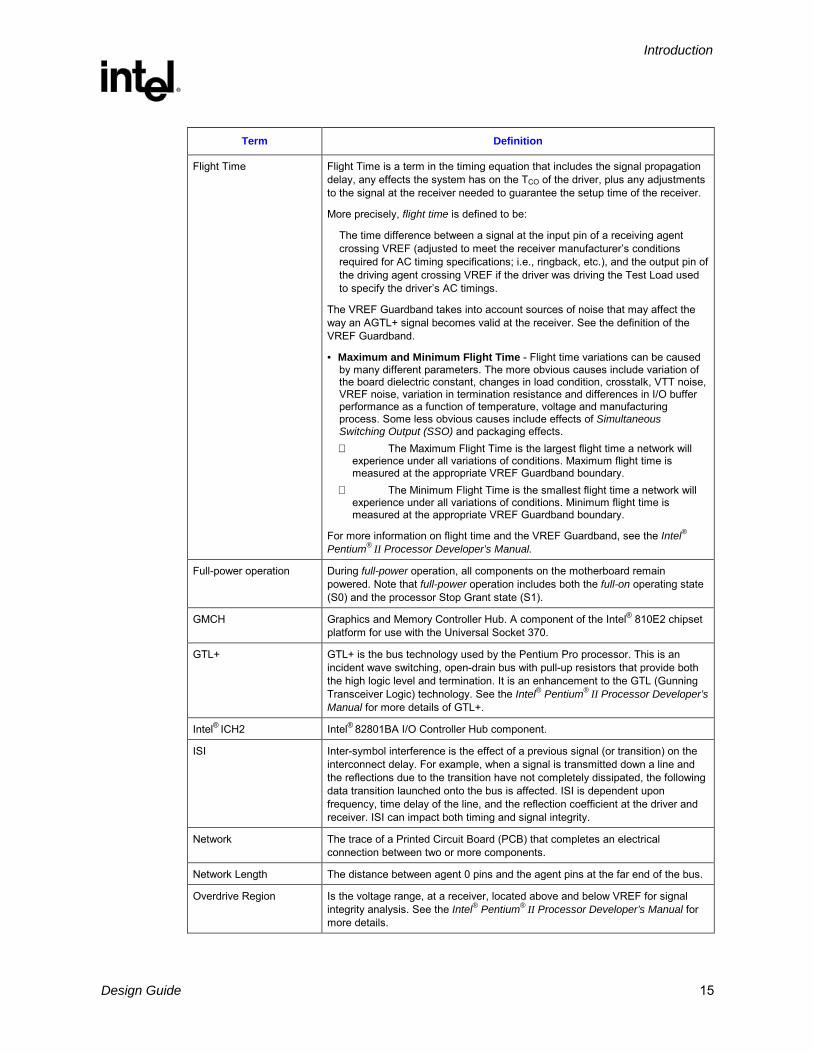
Flight Time Flight Time is a term in the timing equation that includes the signal propagation delay, any effects the system has on the TCO of the driver, plus any adjustments to the signal at the receiver needed to guarantee the setup time of the receiver.
More precisely, flight time is defined to be:
The time difference between a signal at the input pin of a receiving agent crossing VREF (adjusted to meet the receiver manufacturers conditions required for AC timing specifications; i.e., ringback, etc.), and the output pin of the driving agent crossing VREF if the driver was driving the Test Load used to specify the drivers AC timings.
The VREF Guardband takes into account sources of noise that may affect the way an AGTL+ signal becomes valid at the receiver. See the definition of the VREF Guardband.
• Maximum and Minimum Flight Time - Flight time variations can be caused by many different parameters. The more obvious causes include variation of the board dielectric constant, changes in load condition, crosstalk, VTT noise, VREF noise, variation in termination resistance and differences in I/O buffer performance as a function of temperature, voltage and manufacturing process. Some less obvious causes include effects of Simultaneous Switching Output (SSO) and packaging effects. The Maximum Flight Time is the largest flight time a network will
experience under all variations of conditions. Maximum flight time is measured at the appropriate VREF Guardband boundary.
The Minimum Flight Time is the smallest flight time a network will experience under all variations of conditions. Minimum flight time is measured at the appropriate VREF Guardband boundary.
For more information on flight time and the VREF Guardband, see the Intel® Pentium® II Processor Developer’s Manual.
Full-power operation During full-power operation, all components on the motherboard remain powered. Note that full-power operation includes both the full-on operating state (S0) and the processor Stop Grant state (S1).
GMCH Graphics and Memory Controller Hub. A component of the Intel® 810E2 chipset platform for use with the Universal Socket 370.
GTL+ GTL+ is the bus technology used by the Pentium Pro processor. This is an incident wave switching, open-drain bus with pull-up resistors that provide both the high logic level and termination. It is an enhancement to the GTL (Gunning Transceiver Logic) technology. See the Intel® Pentium® II Processor Developer’s Manual for more details of GTL+.
Intel® ICH2 Intel® 82801BA I/O Controller Hub component.
ISI Inter-symbol interference is the effect of a previous signal (or transition) on the interconnect delay. For example, when a signal is transmitted down a line and the reflections due to the transition have not completely dissipated, the following data transition launched onto the bus is affected. ISI is dependent upon frequency, time delay of the line, and the reflection coefficient at the driver and receiver. ISI can impact both timing and signal integrity.
Network The trace of a Printed Circuit Board (PCB) that completes an electrical connection between two or more components.
Network Length The distance between agent 0 pins and the agent pins at the far end of the bus.
Overdrive Region Is the voltage range, at a receiver, located above and below VREF for signal integrity analysis. See the Intel® Pentium® II Processor Developer’s Manual for more details.

Introduction
R
16 Design Guide
Term Definition
Overshoot Maximum voltage allowed for a signal at the processor core pad. See each processors datasheet for overshoot specification.
Pad The electrical contact point of a semiconductor die to the package substrate. A pad is only observable in simulation.
Pin The contact point of a component package to the traces on a substrate such as the motherboard. Signal quality and timings can be measured at the pin.
Power rails An ATX power supply has 6 power rails: +5V, -5V, +12V, -12V, +3.3V, +5VSB. In addition to these power rails, several other power rails can be created with voltage regulators.
Ringback The voltage that a signal rings back to after achieving its maximum absolute value. Ringback may be due to reflections, driver oscillations, or other transmission line phenomena.
Settling Limit Defines the maximum amount of ringing at the receiving pin that a signal must reach before its next transition. See the respective processors datasheet for settling limit specification.
Setup Window The time between the beginning of Setup to Clock (TSU_MIN) and the arrival of a valid clock edge. This window may be different for each type of bus agent in the system.
Simultaneous Switching Output (SSO)
Simultaneous Switching Output (SSO) Effects refers to the difference in electrical timing parameters and degradation in signal quality caused by multiple signal outputs simultaneously switching voltage levels (e.g., high-to-low) in the opposite direction from a single signal (e.g., low-to-high) or in the same direction (e.g., high-to-low). These are respectively called odd-mode switching and even-mode switching. This simultaneous switching of multiple outputs creates higher current swings that may cause additional propagation delay (or push-out), or a decrease in propagation delay (or pull-in). These SSO effects may impact the setup and/or hold times and are not always taken into account by simulations. System timing budgets should include margin for SSO effects.
Standby power rail A power rail that in on during suspend operation (these rails are also on during full-power operation). These rails are on at all times (when the power supply is plugged into AC power). The only standby power rail that is distributed directly from the ATX power supply is 5VSB (5V Standby). There can be other standby rails that are created with voltage regulators.
Stub The branch from the bus trunk terminating at the pad of an agent.
Suspend operation During suspend operation, power is removed from some components on the motherboard. The customer reference board supports three suspend states: processor Stop Grant (S1), Suspend-to-RAM (S3) and Soft-off (S5).
Suspend-to-RAM (STR In the STR state, the system state is stored in main memory and all unnecessary system logic is turned off. Only main memory and logic required to wake the system remain powered.
System Bus The system bus is the processor bus.
Test Load Intel uses a 50 Ω test load for specifying its components.
Trunk The main connection, excluding interconnect branches, from one end agent pad to the other end agent pad.
Undershoot Minimum voltage observed for a signal to extend below VSS at the device pad.
Introduction
R
Design Guide 17
Term Definition
Universal Socket 370 Refers to the 810E2 chipset using the universal PGA370 socket. In general, these designs support 66/100/133 MHz system bus operation, Intel VRM guidelines for future 0.13 micron processors, and Intel® Celeron processors (CPUID=068xh), Intel Pentium III processor (CPUID=068xh), and future Pentium® III processors in single-microprocessor based designs.
Victim A network that receives a coupled crosstalk signal from another network is called the victim network.
VREF Guardband A guardband (DVREF) defined above and below VREF to provide a more realistic model accounting for noise such as crosstalk, VTT noise, and VREF noise.
1.2 Related Documents Document and Location Location
Intel® 810E Chipset: 82810E Graphics and Memory Controller Hub (GMCH) Datasheet
http://developer.intel.com/design/chipsets/datashts/290676.htm
Intel® 82801BA I/O Controller Hub 2 (ICH2) and Intel® 82801 BAM I/O Controller Hub 2 Mobile (ICH2-M) Datasheet
http://developer.intel.com/design/chipsets/datashts/290687.htm
Intel® 82802AB/AC Firmware Hub (FWH) Datasheet http://developer.intel.com/design/chipsets/datashts/290658.htm
Intel® Celeron® Processor Datasheet http://developer.intel.com/design/celeron/datashts/243658.htm
Intel® Celeron® Processor Specification Update http://developer.intel.com/design/celeron/specupdt/243748.htm
CK 810E Clock Synthesizer Driver Specification, r 0.9 Note 1
PPGA 370 Power Delivery Guidelines Note 1
Pentium® III Processor for the SC242 at 450 MHz to 1.13 GHz Datasheet
http://developer.intel.com/design/pentiumiii/datashts/244452.htm
Intel® Pentium® III Processor Specification Update http://developer.intel.com/design/pentiumiii/specupdt/244453.htm
Intel® Pentium® III Power Distribution Guidelines (AP-907) Application Note
http://developer.intel.com/design/pentiumiii/applnots/245085.htm
PCI Local Bus Specification, Revision 2.2 http://www.pcisig.com/
Universal Serial Bus Specification, Revision 1.0 http://www.usb.org/developers/docs.html
Intel® 82562ET Platform LAN Connect (PLC) Datasheet Note 1
PCB Design for the Intel® 82562 ET/EM Platform LAN Connect
Note 1
Intel® 82562EH HomePNA 1 Mb/s Physical Layer Interface Brief Datasheet
http://www.intel.com/design/network/index.htm
NOTES: 1. Contact your Intel representative for the current revision of this document.

Introduction
R
18 Design Guide
1.3 System Overview The Intel 810E2 chipset platform for use with the universal socket 370 contains a Graphics and Memory Controller Hub (GMCH) component and I/O Controller Hub 2 (ICH2) component for desktop platforms.
The GMCH provides the processor interface optimized for future 0.13 micron 370 socket processors, DRAM interface, hub interface, and internal graphics. This product provides flexibility and scalability in graphics and memory subsystem performance.
The Accelerated Hub Architecture interface (i.e., the chipset component interconnect) is designed into the chipset to provide an efficient, high-bandwidth communication channel between the GMCH and the I/O controller hub. The chipset architecture also enables a security and manageability infrastructure through the firmware hub component.
An ACPI-compliant Intel 810E2 chipset universal platform can support the Full-on (S0), Stop Grant (S1), Suspend to RAM (S3), Suspend to Disk (S4), and Soft-off (S5) power management states. The chipset also supports wake-on-LAN* for remote administration and troubleshooting. The chipset architecture removes the requirement for the ISA expansion bus that was traditionally integrated into the I/O subsystem of PCIsets/AGPsets. This removes many of the conflicts experienced when installing hardware and drivers into legacy ISA systems. The elimination of ISA provides true plug-and-play for the platform. Traditionally, the ISA interface was used for audio and modem devices. The addition of AC’97 allows the OEM to use software-configurable AC’97 audio and modem coder/decoders (codecs), instead of the traditional ISA devices.
The Intel 810E2 chipset contains two core components:
• Intel 82810E2 Graphics and Memory Controller Hub (GMCH)
• Intel 82801BA I/O Controller Hub 2 (ICH2)
The GMCH integrates a 66/100/133 MHz, P6 family system bus controller, integrated 2D/3D graphics accelerator, 100 MHz SDRAM controller and a high-speed hub interface for communication with the I/O Controller Hub (ICH2). The ICH2 integrates an Ultra ATA/100 controller, 2 USB host controllers with a total of 4 ports, LPC interface controller, FWH Flash BIOS interface controller, PCI interface controller, AC ’97 digital controller and a hub interface for communication with the GMCH.
1.3.1 System Features
The Intel 810E2 chipset platform contains two components: the Intel 82810E Graphics and Memory Controller Hub (GMCH) and the Intel 82801BA I/O Controller Hub 2 (ICH2). The GMCH integrates a 66/100/133 MHz, P6 family system bus controller, integrated 2D/3D graphics accelerator, 100 MHz SDRAM controller, and a high-speed accelerated hub architecture interface for communication with the ICH2. The ICH2 integrates an UltraATA/100 controller, two Universal Serial Bus (USB) host controllers with a total of four ports, Low Pin Count (LPC) interface controller, Firmware Hub (FWH) interface controller, PCI interface controller, AC-link, integrated LAN controller, and a hub interface for communication with the GMCH.
Introduction
R
Design Guide 19
1.3.2 Component Features
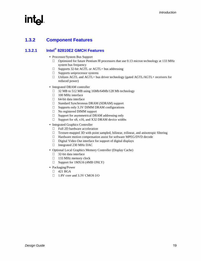
1.3.2.1 Intel® 82810E2 GMCH Features • Processor/System Bus Support
Optimized for future Pentium III processors that use 0.13 micron technology at 133 MHz system bus frequency
Supports 32-bit AGTL or AGTL+ bus addressing Supports uniprocessor systems Utilizes AGTL and AGTL+ bus driver technology (gated AGTL/AGTL+ receivers for
reduced power)
• Integrated DRAM controller 32 MB to 512 MB using 16Mb/64Mb/128 Mb technology 100 MHz interface 64-bit data interface Standard Synchronous DRAM (SDRAM) support Supports only 3.3V DIMM DRAM configurations No registered DIMM support Support for asymmetrical DRAM addressing only Support for x8, x16, and X32 DRAM device widths
• Integrated Graphics Controller Full 2D hardware acceleration Texture-mapped 3D with point sampled, bilinear, trilinear, and anisotropic filtering Hardware motion compensation assist for software MPEG/DVD decode Digital Video Out interface for support of digital displays Integrated 230 MHz DAC
• Optional Local Graphics Memory Controller (Display Cache) 32-bit data interface 133 MHz memory clock Support for 1MX16 (4MB ONLY)
• Packaging/Power 421 BGA 1.8V core and 3.3V CMOS I/O

Introduction
R
20 Design Guide
1.3.2.2 Intel® 82801BA I/O Controller Hub 2 (ICH2) The ICH2 allows the I/O subsystem to access the rest of the system, as follows:
• Upstream accelerated hub architecture interface for access to the GMCH • PCI 2.2 interface (6 PCI Request/Grant pairs) • 2 channel Ultra ATA/100 Bus Master IDE controller • USB controller (Expanded capabilities for 4 ports) • I/O APIC • SMBus controller • FWH interface • LPC interface • AC’97 2.1 interface • Integrated system management controller • Alert-on-LAN* • Integrated LAN controller • Packaging/Power
360 EBGA 1.8V (± 3% within margins of 1.795 V to 1.9 V) core and 3.3V standby
1.3.2.3 Firmware Hub (FWH)
The hardware features of the firmware hub include:
• An integrated hardware Random Number Generator (RNG)
• Register-based locking
• Hardware-based locking
• 5 General Purpose Interrupts (GPI)
• Packaging/Power 40L TSOP and 32L PLCC 3.3V core and 3.3V / 12V for fast programming

Introduction
R
Design Guide 21
1.3.3 System Configurations
Figure 1. Intel® 810E2 Chipset System
System Bus (100/133 MHz)
SystemMemory
sysblk2
Intel® 82810E2(GMCH)
- Memory Controller- Graphcs Controller - 3D Engine - 2D Engine - Video Engine
TV
Display
Encoder
(4 MB SDRAM)
Display Cache
64 Bit /100 MHz Only
Intel® 810E2Chipset
Digital Video Out
Processor
I/O Controller Hub(82801BA ICH2)
PCI Bus
ISABridge
(optional)
4 USB Ports; 2 HC
UltraATA/100/66/33
AC'97Codec(s)(optional)
AC'97 2.1
LPC I/FSuper I/O
Keyboard,Mouse, FD, PP,
SP, IR
FWH FlashBIOS
PCISlots
ISASlots
PCIAgent
GPIOLAN Connect
4 IDE Drives
Hub Interface

Introduction
R
22 Design Guide
1.4 Platform Initiatives
1.4.1 Hub Interface
As I/O speeds increase, the demand placed on the PCI bus by the I/O bridge has become significant. With the addition of AC’97 and Ultra ATA/100, coupled with the existing USB, I/O requirements could impact PCI bus performance. The 810E2 chipset’s hub interface architecture ensures that the I/O subsystem (both PCI and the integrated I/O features such as IDE, AC’97, USB, etc.), receives adequate bandwidth. By placing the I/O bridge on the hub interface (instead of PCI), the hub architecture ensures that both the I/O functions integrated into the ICH2 and the PCI peripherals obtain the bandwidth necessary for peak performance.
1.4.2 Integrated LAN Controller
The 810E2 chipset platform incorporates an ICH2 integrated LAN Controller. Its bus master capabilities enable the component to process high-level commands and perform multiple operations; this lowers processor utilization by off-loading communication tasks from the processor.
The ICH2 functions with several options of LAN connect components to target the desired market segment. The Intel 82562EH provides a HomePNA 1 Mbit/sec connection. The Intel 82562ET provides a basic Ethernet 10/100 connection. The Intel 82562EM provides an Ethernet 10/100 connection with the added flexibility of Alert on LAN.
1.4.3 Ultra ATA/100 Support
The 810E2 chipset platform incorporates the ICH2 IDE controller with two sets of interface signals (primary and secondary) that can be independently enabled, tri-stated or driven low. The platform supports Ultra ATA/100 for transfers up to 100 MB/sec, in addition to Ultra ATA/66 and Ultra ATA/33 modes.
1.4.4 Expanded USB Support
The 810E2 chipset platform contains two USB Host Controllers. Each Host Controller includes a root hub with two separate USB ports each, for a total of 4 USB ports. The addition of a second USB Host Controller expands the functionality of the platform.
1.4.5 SMBus
The ICH2 integrates a SMBus controller. The SMBus provides an interface for managing peripherals such as serial presence detection (SPD) and thermal sensors. The slave interface allows an external microcontroller to access system resources.
Introduction
R
Design Guide 23
1.4.6 Interrupt Controller
The interrupt capabilities of the 810E2 chipset platform expand support for up to 8 PCI interrupt pins and PCI 2.2 message-based interrupts. In addition, the ICH2 supports system bus interrupt delivery.
1.4.7 Firmware Hub (FWH) Flash BIOS
The 810ET2 chipset platform supports firmware hub BIOS memory sizes up to 8 MB for increased system flexibility.
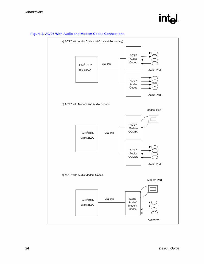
1.4.8 AC ’97 6-Channel Support
The Audio Codec ’97 (AC’97) Specification defines a digital interface that can be used to attach an audio codec (AC), a modem codec (MC), an audio/modem codec (AMC), or both an AC and a MC. The AC’97 Specification defines the interface between the system logic and the audio or modem codec known as the AC-link.
The 810E2 chipset platform’s AC ’97 (with the appropriate codecs) not only replaces ISA audio and modem functionality, but also improves overall platform integration by incorporating the AC-link. Using 810E2 chipset’s integrated AC-link reduces cost and eases migration from ISA.
By using an audio codec, the AC-link allows for cost-effective, high-quality, integrated audio on the 810E2 chipset platform. In addition, an AC ’97 soft modem can be implemented with the use of a modem codec. Several system options exist when implementing AC ’97. The 810ET2 chipset’s integrated digital link allows several external codecs to be connected to the ICH2. The system designer can provide audio with an audio codec, a modem with a modem codec, or an integrated audio/modem codec. The digital link is expanded to support two audio codecs or a combination of an audio and modem codec.
Modem implementation for different countries must be taken into consideration, as telephone systems may vary. By implementing a split design, the audio codec can be on board and the modem codec can be placed on a riser. Intel is developing a Communications and Networking Riser connector.
The digital link in the ICH2 is AC’97 Rev. 2.1 compliant, supporting two codecs with independent PCI functions for audio and modem. Microphone input and left and right audio channels are supported for a high-quality, two-speaker audio solution. Wake-on-ring-from-suspend also is supported with the appropriate modem codec.
The 810E2 chipset platform expands audio capability with support for up to six channels of PCM audio output (i.e., full AC3 decode). Six-channel audio consists of Front Left, Front Right, Back Left, Back Right, Center and Woofer, for a complete surround sound effect. ICH2 has expanded support for two audio codecs on the AC’97 digital link.
Introduction
R
24 Design Guide
Figure 2. AC'97 With Audio and Modem Codec Connections
AC97 Modem CODEC
Modem Port
Audio Port
AC97 Audio/
CODEC
AC97 Audio Codec AC-link
AC97 Audio Codec
Audio Port
Audio Port
Intel® ICH2
360 EBGA AC97Audio/ ModemCodec
Audio Port
Modem Port
a) AC'97 with Audio Codecs (4-Channel Secondary)
b) AC'97 with Modem and Audio Codecs
c) AC'97 with Audio/Modem Codec
AC-link
AC-link
Intel® ICH2
360 EBGA
Intel® ICH2 360 EBGA

Introduction
R
Design Guide 25
1.4.9 Low Pin Count (LPC) Interface
In the 810E2 chipset platform, the Super I/O (SIO) component has migrated to the Low-Pin-Count (LPC) interface. Migration to the LPC interface allows for lower-cost Super I/O designs. The LPC Super I/O component requires the same feature set as traditional Super I/O components. It should include a keyboard and mouse controller, floppy disk controller, and serial and parallel ports. In addition to the Super I/O features, an integrated game port is recommended because the AC’97 interface does not provide support for a game port. In systems with ISA audio, the game port typically existed on the audio card. The fifteen-pin game port connector provides for two joysticks and a two-wire MPU-401 MIDI interface. Consult your preferred Super I/O vendor for a comprehensive list of the devices offered and the features supported.
In addition, depending on system requirements, specific system I/O requirements may be integrated into the LPC Super I/O. For example, a USB hub may be integrated to connect to the ICH2 USB output and extend it to multiple USB connectors. Other SIO integration targets include a device bay controller or an ISA-IRQ-to-serial-IRQ converter to support a PCI-to-ISA bridge. Contact your Super I/O vendor to ensure the availability of desired LPC Super I/O features.

Introduction
R
26 Design Guide
This page is intentionally left blank.

General Design Considerations
R
Design Guide 27
2 General Design Considerations This design guide documents motherboard layout and routing guidelines for 810E2 universal socket 370 platform-based systems. This design guide does not discuss the functional aspects of any bus or the layout guidelines for an add-in device.
If the guidelines listed in this document are not followed, it is very important that thorough signal integrity and timing simulations be completed for each design. Even when the guidelines are followed, critical signals should be simulated to ensure the proper signal integrity and flight time. As bus speeds increase, it is imperative that the guidelines documented are followed precisely. Any deviation from these guidelines should be simulated.
The trace impedance typically noted (i.e., 60 Ω ± 15%) is the “nominal” trace impedance for a 5-mil-wide trace. That is, it is the impedance of the trace when not subjected to the fields created by changing current in neighboring traces. When calculating flight times, it is important to consider the minimum and maximum impedance of a trace, based on the switching of neighboring traces. The use of wider spaces between the traces can minimize this trace-to-trace coupling. In addition, these wider spaces reduce crosstalk and settling time.
Coupling between two traces is a function of the coupled length, the distance separating the traces, the signal edge rate, and the degree of mutual capacitance and inductance. To minimize the effects of trace-to-trace coupling, follow the routing guidelines documented in this section.
Additionally, these routing guidelines are created using a PCB stack-up similar to that illustrated in Figure 3.
2.1 Nominal Board Stack-Up The 810E2 chipset universal platform requires a board stack-up yielding a target impedance of 60 Ω ± 10% with a 5 mil nominal trace width. Figure 3 presents an example stack-up that achieves this. It is a 4-layer printed circuit board (PCB) construction using 53%-resin FR4 material.
Figure 3. Board Construction Example for 60 ΩΩΩΩ Nominal Stack-Up
board_4.5mil_stackup
~48-mil core
Component-side layer 1: ½ oz. Cu
Power plane layer 2: 1 oz. Cu4.5-mil prepreg
Ground layer 3: 1 oz. Cu
Solder-side layer 4: ½ oz. Cu4.5-mil prepreg
Total thickness:62 mils

General Design Considerations
R
28 Design Guide
This page is intentionally left blank.
Component Layouts
R
Design Guide 29
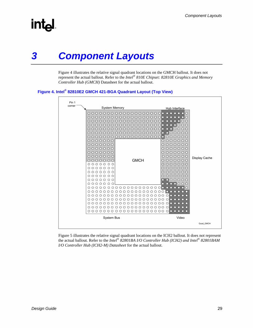
3 Component Layouts Figure 4 illustrates the relative signal quadrant locations on the GMCH ballout. It does not represent the actual ballout. Refer to the Intel® 810E Chipset: 82810E Graphics and Memory Controller Hub (GMCH) Datasheet for the actual ballout.
Figure 4. Intel® 82810E2 GMCH 421-BGA Quadrant Layout (Top View)
Quad_GMCH
GMCH
System Memory
Display Cache
Video
Hub Interface
System Bus
Pin 1corner
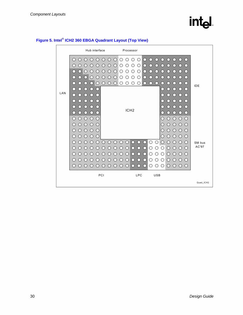
Figure 5 illustrates the relative signal quadrant locations on the ICH2 ballout. It does not represent the actual ballout. Refer to the Intel® 82801BA I/O Controller Hub (ICH2) and Intel® 82801BAM I/O Controller Hub (ICH2-M) Datasheet for the actual ballout.
Component Layouts
R
30 Design Guide
Figure 5. Intel® ICH2 360 EBGA Quadrant Layout (Top View)
SM busAC'97
Hub interface Processor
PCI LPC USB
Quad_ICH2
LAN
IDE
ICH2

Component Layouts
R
Design Guide 31
Figure 6. Firmware Hub (FWH) Packages
pck_fwh.vsd
1234567891011121314151617181920
4039383736353433323130292827262524232221
FWH Interface
(40-Lead TSOP)
5
6
7
8
9
10
11
12
13
29
28
27
26
25
24
23
22
21
1234 32 31 30
14 15 16 17 18 19 20
FWH Interface
(32-Lead PLCC,0.450" x 0.550")
Top View

Component Layouts
R
32 Design Guide
This page is intentionally left blank.

Universal Motherboard Design
R
Design Guide 33
4 Universal Motherboard Design
4.1 Universal Motherboard Definition Details The universal socket 370 platform supports Pentium III processor (CPUID=068xh) and Celeron processor (CPUID=068xh) as well as future 0.13 micron socket 370 processors. The Pentium III processor (CPUID=068xh) and Celeron processor (CPUID=068xh) have different requirements for functioning properly in a platform than the future 0.13 micron socket 370 processors. It is necessary to understand these differences and how they affect the design of the platform. Refer to Table 1 through Table 3 for a high-level description of the differences that require additional circuitry on the motherboard. Specific details on implementing this circuitry are discussed further in this chapter. For a detailed description of the pin differences between the Pentium III processor (CPUID=068xh) / Celeron processor (CPUID=068xh), and future 0.13 micron socket 370 processor pins, refer to Section 5.4.
Table 1. Processor Considerations for Universal Motherboard Design
Signal Name or Pin
Number
Function In Intel® Pentium® III
Processor (CPUID=068xh) and
Intel® Celeron® Processor
(CPUID=068xh)
Function In Future
0.13 Micron Socket 370 Processors
Implementation for Universal Socket 370 Design
AF36 VSS No connect Addition of circuitry that generates a processor identification signal used to configure board-level operation.
AG1 VSS VTT Addition of FET switch to ground or VTT, controlled by processor identification signal.
Note: FET must have no more than 100 milliohms resistance between source and drain.
AJ3 NC NC PGA 370 socket pin AJ3 is a “NC” (no connect) for either processor.
AK22 GTL_REF VCMOS_REF Addition of resistor-divider network to provide 1.0V, which will satisfy voltage tolerance requirements of the Intel®
Pentium III processor (CPUID=068xh) and Intel® Celeron® processor (CPUID=068xh) as well as future 0.13 micron socket 370 processors.
PICCLK Requires 2.5V Requires 2.0V Addition of FET switch to provide proper voltage, controlled by processor identification signal.

Universal Motherboard Design
R
34 Design Guide
Signal Name or Pin
Number
Function In Intel® Pentium® III
Processor (CPUID=068xh) and
Intel® Celeron® Processor
(CPUID=068xh)
Function In Future
0.13 Micron Socket 370 Processors
Implementation for Universal Socket 370 Design
PWRGOOD Requires 2.5V Requires 1.8V Addition of resistor-divider network to provide 2.1V, which will satisfy voltage tolerance requirements of the Pentium III processor (CPUID=068xh) and Celeron processor (CPUID=068xh) as well as future 0.13 micron socket 370 processors.
VTT Requires 1.5V Requires 1.25V Modification to VTT generation circuit to switch between 1.5V or 1.25V, controlled by processor identification signal.
VTTPWRGD Not used Input signal to future 0.13 micron socket 370 processors to indicate that VID signals are stable
Addition of VTTPWRGD generation circuit.
Table 2. Intel® ICH2 Considerations for Universal Motherboard Design
Signal Issue Implementation For Universal Motherboard Design
PWROK GMCH and CK810 must not sample BSEL[1:0] until VTTPWRGD asserted. Intel® ICH2 must not initialize before CK810 clocks stabilize
Addition of circuitry to have VTTPWRGD gate PWROK from power supply to ICH2. The ICH2 will hold GMCH in reset until VTTPWRGD asserted plus 20 ms time delay to allow CK810 clocks to stabilize
Table 3. Clock Synthesizer Considerations for Universal Motherboard Design
Signal Issue Implementation For Universal Motherboard Design
VDD CK810 does not support VTTPWRGD
Addition of a FET switch, which supplies power to VDD only when VTTPWRGD is asserted.
Note: FET must have no more than 100 milliohms resistance between source and drain.

Universal Motherboard Design
R
Design Guide 35
4.2 Processor Design Requirements
4.2.1 Use of Universal Motherboard Design with the Intel® 82810E2 GMCH
The universal socket 370 design is intended for use with the 810E2 chipset platform for use with the universal socket 370. A universal socket 370 design populated with an A3 stepping of the GMCH is compatible with future 0.13 micron socket 370 processors.
4.2.2 Identifying the Processor at the Socket
For the platform to configure for the requirements of the processor in the socket, it must first identify whether the processor is a Pentium III processor (CPUID=068xh) / Celeron processor (CPUID=068xh), or a future 0.13 micron socket 370 processors. Pin AF36 is a ground pin on a Pentium III processor (CPUID=068xh) and Celeron processor (CPUID=068xh); pin AF36 is an unconnected pin on future 0.13 micron Socket 370 processors. Referring to Figure 7, the platform uses a detect circuit connected to this processor pin. If a future 0.13 micron Socket 370 processor is present in the socket, the TUAL5 reference schematic signal will be pulled to the 5V rail and the TUAL5# reference schematic signal will be pulled to ground. Otherwise, for a Pentium III processor (CPUID=068xh) or Celeron processor (CPUID=068xh), the TUAL5 reference schematic signal will be pulled to ground and the TUAL5# will be pulled to the 5V rail.
Figure 7. Processor Detect Mechanism at Socket/TUAL5 Generation Circuit
1 KΩ
2.2 KΩ
2.2 KΩVTT
VCC5
VCC5
TUAL5
TUAL5#
MOSFET N
NPNProcessor PinDETECT
Proc_Detect

Universal Motherboard Design
R
36 Design Guide
4.2.3 Setting Processor Auto-Detect
A processor auto-detect circuit for the functionality is shown as Figure 7, Section 4.2.2. A circuit that can use the processor auto-detect information to set LMD26 appropriately is shown as Figure 8 below.
Figure 8. Processor Auto-Detect Circuit for LMD 26
R18.2K
Q12N7002
VCC3_3
TUAL5
LMD26

Universal Motherboard Design
R
Design Guide 37
4.2.4 Setting the Appropriate Processor VTT Level
Because the Pentium III processor (CPUID=068xh) / Celeron processor (CPUID=068xh), and future 0.13 micron socket 370 processors require different VTT levels, the platform must be able to provide the appropriate voltage level after determining which processor is in the socket. Referring to Figure 9, the TUAL5 reference schematic signal serves to control the FET, and by doing so determines whether the voltage regulator supplies 1.25V or 1.5V to VTT for AGTL or AGTL+, respectively.
Figure 9. VTT Selection Switch
VinVout
ADJ
VCC3_3
10 µF
LT1587-ADJ
TUAL5
MOSFET N10 Ω1%
49.9 Ω1%
0.1 µF
22 µFTantalum
VTT
Vtt_Sel_Sw
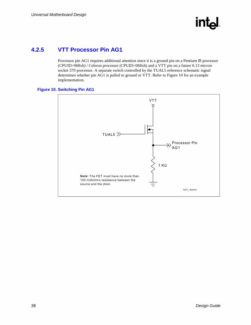
Universal Motherboard Design
R
38 Design Guide
4.2.5 VTT Processor Pin AG1
Processor pin AG1 requires additional attention since it is a ground pin on a Pentium III processor (CPUID=068xh) / Celeron processor (CPUID=068xh) and a VTT pin on a future 0.13 micron socket 370 processor. A separate switch controlled by the TUAL5 reference schematic signal determines whether pin AG1 is pulled to ground or VTT. Refer to Figure 10 for an example implementation.
Figure 10. Switching Pin AG1
1 KΩ
Processor PinAG1
TUAL5
VTT
Note: The FET must have no more than100 milliohms resistance between thesource and the drain.
AG1_Switch

Universal Motherboard Design
R
Design Guide 39
4.2.6 Configuring Non-VTT Processor Pins
When asserted, the VTTPWGRD signal must be level-shifted to 12V to properly drive the gating circuitry of the CK810. Furthermore, while the VTTPWRGD signal is connected to the VTTPWRGD pin on a future 0.13 micron socket 370 processor, on a Pentium III processor (CPUID=068xh) or Celeron processor (CPUID=068xh) that same pin is a ground. To provide proper functionality, a 1.0 kΩ resistor must be placed in series between the circuitry that generates the signal VTTPWRGD and the processor pin VTTPWRGD. Refer to Figure 11 for an example implementation. Voltage regulators that generate the standard VTTPWRGD signal are available.
Figure 11. VTTPWRGD Configuration Circuit
5
3
2
4
VTT
VCC5
V1_8SB
732 Ω1%
1 Κ Ω1%
Vcc
IN+ 1
IN- 1
Gnd
2
3
1
VCC5
VTTPW RGD_Config
1
BAT54C
V1_8SB
8
76IN+ 2
IN- 2Out 1
Out 2
VCC5
20 KΩ
VCC5
1 KΩ
VTTPW RGD5#
LM393 Ch2LM393 Ch1 0.1 µF
VTTPW RGD
1 KΩ
1 KΩ
VTT
VTTPW RGD12
2.2 KΩ
VCC12
2.0 ms delay nominal
MOSFET N
MOSFET N
ASSERTEDLOW
NOTE: The diode is included so that repeated pressing of the reset or power button does not cause the capacitor to build up enough charge to circumvent the 20 ms delay.

Universal Motherboard Design
R
40 Design Guide
4.2.7 VCMOS Reference
In previous platforms supporting the Pentium III processor (CPUID=068xh) and Celeron processor (CPUID=068xh), VCMOS was generated by the same power plane as VTT. The future 0.13 micron socket 370 processors do not generate VCMOS, and the universal platform is required to generate this separately on the motherboard. Processor pin AK22, which is a GTL_REF pin on a Pentium III processor (CPUID=068xh) and Celeron processor (CPUID=068xh), has been changed to a VCMOS_REF pin on future 0.13 micron socket 370 processors. Referring to Figure 12, a network of resistors and a capacitor must be added so that this pin operates appropriately for whichever processor is in the socket).
Figure 12. GTL_REF/VCMOS_REF Voltage Divider Network
75 Ω1%
150 Ω1%
VCMOS
Processor PinAK22
0.1 µF
GTL_CMOS_Ref

Universal Motherboard Design
R
Design Guide 41
4.2.8 Processor Signal PWRGOOD
The processor signal PWRGOOD is specified at different voltage levels depending on whether it is a Pentium III processor (CPUID=068xh) / Celeron processor (CPUID=068xh), or whether it is a future 0.13 micron socket 370 processor. As there is an overlap between the ranges of accepted voltage levels for these two processor groups, a resistor divider network that provides 2.1V will satisfy the requirements of all supported processors. See Figure 13 for an example implementation.
Figure 13. Resistor Divider Network for Processor PWRGOOD
PW RGOOD to Processor
VCC2_5
PW RGOOD from ICH2
330 Ω
1.8 Κ Ω
PW RGOOD_Divider

Universal Motherboard Design
R
42 Design Guide
4.2.9 APIC Clock Voltage Switching Requirements
The processor’s APIC clock is also specified at different voltage levels depending on whether it is for the Pentium III processor (CPUID=068xh) / Celeron processor (CPUID=068xh) or whether it is for a future 0.13 micron socket 370 processor. There is no overlap in the range of accepted voltage levels for the two processor groups, so a voltage switch is required to ensure proper operation. Figure 14 shows an example implementation.
Figure 14 Voltage Switch for Processor APIC Clock
30 Ω
130 Ω
IOAPIC
APICCLK_CPU
TUAL5
MOSFET N
API_CLK_SW
NOTE: The 30 Ω resistor represents the series resistor typically used in connecting the APIC clock to the processor.
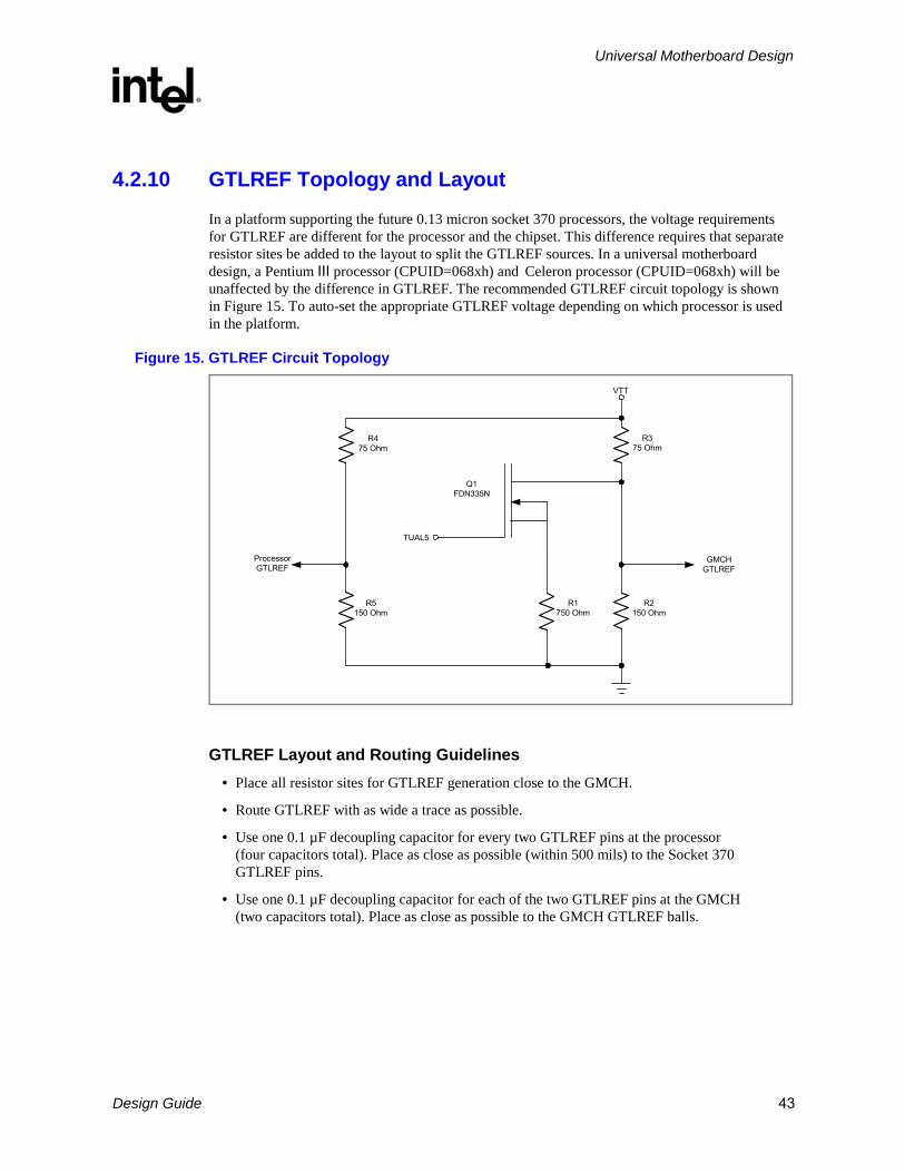
Universal Motherboard Design
R
Design Guide 43
4.2.10 GTLREF Topology and Layout
In a platform supporting the future 0.13 micron socket 370 processors, the voltage requirements for GTLREF are different for the processor and the chipset. This difference requires that separate resistor sites be added to the layout to split the GTLREF sources. In a universal motherboard design, a Pentium III processor (CPUID=068xh) and Celeron processor (CPUID=068xh) will be unaffected by the difference in GTLREF. The recommended GTLREF circuit topology is shown in Figure 15. To auto-set the appropriate GTLREF voltage depending on which processor is used in the platform.
Figure 15. GTLREF Circuit Topology
R1750 Ohm
TUAL5
R2150 Ohm
VTT
GMCHGTLREF
Q1FDN335N
R375 Ohm
R475 Ohm
R5150 Ohm
ProcessorGTLREF
GTLREF Layout and Routing Guidelines • Place all resistor sites for GTLREF generation close to the GMCH.
• Route GTLREF with as wide a trace as possible.
• Use one 0.1 µF decoupling capacitor for every two GTLREF pins at the processor (four capacitors total). Place as close as possible (within 500 mils) to the Socket 370 GTLREF pins.
• Use one 0.1 µF decoupling capacitor for each of the two GTLREF pins at the GMCH (two capacitors total). Place as close as possible to the GMCH GTLREF balls.

Universal Motherboard Design
R
44 Design Guide
4.3 Power Sequencing on Wake Events In addition to the mechanism for identifying the processor in the socket, special handling of wake events is required for 810E2 chipset universal platforms that support functionality of future 0.13 micron socket 370 processors. When a wake event is triggered, the GMCH and the CK810 must not sample BSEL[1:0] until the signal VTTPWRGD is asserted. This is handled by setting up the following sequence of events: 1. Power is not connected to the CK810-compliant clock driver until VTTPWRGD12 is
asserted. 2. Clocks to the ICH2 stabilize before the power supply asserts PWROK to the ICH2. There is
no guarantee this will occur as the implementation for the previous step relies on the 12 V supply. Thus it is necessary to gate PWROK to the ICH2 from the power supply while the CK810 is given sufficient time for the clocks to become stable. The amount of time required is a minimum 20 ms.
3. ICH2 takes the GMCH out of reset. 4. GMCH samples BSEL[1:0]. (CK-815 will have sampled BSEL[1:0] much earlier.)
4.3.1 Gating of CK810 to VTTPWRGD
System designers must ensure that the VTTPWRGD signal is asserted before the CK810-compliant clock driver receives power. This is handled by having the 3.3 V rail of the clock driver gated by the VTTPWRGD12 reference schematic signal. Unlike previous 810E chipset designs, the 3.3 V standby rail is not used to power the clock as the VTTPWRGD12 reference schematic signal will cut power to the clock when going into any sleep state. Refer to Figure 16 for an example implementation.
Figure 16. Gating Power to CK810
VCC3_3
VDD on CK-810VTTPW RGD12
MOSFET N
Note: The FET must have no more than100 milliohms resistance between thesource and the drain.
Gating_Pwr

Universal Motherboard Design
R
Design Guide 45
4.3.2 Gating of PWROK to Intel® ICH2
With power being gated to the CK810 by the signal VTTPWRGD12, it is important that the clocks to the ICH2 are stable before the power supply asserts PWROK to the ICH2. As the clocking power gating circuitry relies on the 12 V supply, there is no guarantee that these conditions will be met. This is why an estimated minimum time delay of 20ms must be added after power is connected to the CK810 to give the clock driver sufficient time to stabilize. This time delay will gate the power supply’s assertion of PWROK to the ICH2. After the time delay, the power supply can safely assert PWROK to the ICH2, with the ICH2 subsequently taking the GMCH out of reset. Refer to Figure 17 for an example implementation.
Figure 17 PWROK Gating Circuit for Intel® ICH2
43 kΩ
PW ROK
ICH2_PW ROK_GATING
Note:Delay 20 ms after VDDon CK-810 is powered
VDD on CK-810 VCC3_3
ICH2_PW ROK1.0 µF
NOTE: The diode is included so that repeated pressing of the reset or power button does not cause the capacitor to build up enough charge to circumvent the 20ms delay.

Universal Motherboard Design
R
46 Design Guide
This page is intentionally left blank.

System Bus Design Guidelines
R
Design Guide 47
5 System Bus Design Guidelines The Pentium III processor delivers higher performance by integrating the Level 2 cache into the processor and running it at the processor's core speed. The Pentium III processor runs at higher core and system bus speeds than previous-generation IA-32 processors while maintaining hardware and software compatibility with earlier Pentium III processors. The new Flip Chip-Pin Grid Array 2 (FC-PGA2) package technology enables compatibility with previous Flip Chip-Pin Grid Array (FC-PGA) packages using the PGA370 socket.
This section presents the considerations for designs capable of using the 810E2 chipset universal platform with the full range of Pentium III processors using the PGA370 socket.
5.1 System Bus Routing Guidelines The following layout guide supports designs using Pentium III processor (CPUID=068xh) / Celeron processor (CPUID=068xh), and future 0.13 micron socket 370 processors with the 810E2 chipset platform. The solution covers system bus speeds of 66/100/133 MHz for the Pentium III processor (CPUID=068xh) / Celeron processor (CPUID=068xh), and future 0.13 micron socket 370 processors. All processors must also be configured to 56 Ω on-die termination.
5.1.1 Initial Timing Analysis
Table 4 lists the AGTL/AGTL+ component timings of the processors and 810E2 chipset universal platform’s GMCH defined at the pins. These timings are for reference only. Obtain each processor’s specifications from its respective processor datasheet and the chipset values from the appropriate 810E2 chipset datasheet.

System Bus Design Guidelines
R
48 Design Guide
Table 4. Intel® Pentium® III Processor AGTL/AGTL+ Parameters for Example Calculations
IC Parameters Intel® Pentium® III Processor at 133 MHz System Bus
Intel® 82810E2 GMCH
Notes
Clock to Output maximum (TCO_MAX)
3.25 ns (for 66/100/133 MHz system bus speeds)
4.1 ns 1, 2
Clock to Output minimum (TCO_MIN) 0.40 ns (for 66/100/133 MHz system bus)
1.05 ns 1, 2
Setup time (TSU_MIN) 1.20 ns for BREQ Lines
0.95 ns for all other AGTL/AGTL+ Lines @ 133 MHz
1.20 ns for all other AGTL/AGTL+ Lines @ 66/100 MHz
2.65 ns 1, 2,3
Hold time (THOLD) 1.0 ns (for 66/100/133 MHz system bus speeds)
0.10 ns 1
NOTES: 1. All times in nanoseconds. 2. Numbers in table are for reference only. These timing parameters are subject to change. Check the
appropriate component documentation for the valid timing parameter values. 3. TSU_MIN = 2.65 ns assumes that the GMCH sees a minimum edge rate equal to 0.3 V/ns.
Table 5 contains an example AGTL+ initial maximum flight time, and Table 6 contains an example minimum flight time calculation for a 133 MHz, uniprocessor system using the Pentium III processor and the 810E2 chipset universal platform’s system bus. Note that assumed values were used for the clock skew and clock jitter. The clock skew and clock jitter values depend on the clock components and the distribution method chosen for a particular design and must be budgeted into the initial timing equations, as appropriate for each design.
Table 5 and Table 6 were derived assuming the following:
• CLKSKEW = 0.20 ns (Note: This assumes that the clock driver pin-to-pin skew is reduced to 50 ps by tying the two host clock outputs together (i.e., “ganging”) at the clock driver output pins, and that the PCB clock routing skew is 150 ps. The system timing budget must assume 0.175 ns of clock driver skew if outputs are not tied together as well as the use of a clock driver that meets the CK810 Clock Synthesizer/Driver Specification.)
• CLKJITTER = 0.250 ns
See the respective processor’s datasheet, the appropriate 810E2 chipset universal documentation, and the CK810 Clock Synthesizer/Driver Specification for details on clock skew and jitter specifications. Exact details regarding the host clock routing topology are provided with the platform design guideline.

System Bus Design Guidelines
R
Design Guide 49
Table 5. Example TFLT_MAX Calculations for 133 MHz Bus
Driver Receiver Clk Period2
TCO_MAX TSU_MIN ClkSKEW ClkJITTER MADJ Recommended TFLT_MAX
Processor GMCH 7.50 3.25 2.65 0.20 0.25 0.40 1.1
GMCH Processor 7.50 4.1 1.20 0.20 0.25 0.40 1.35
NOTES: 1. All times in nanoseconds 2. BCLK period = 7.50 ns @ 133.33 MHz
Table 6. Example TFLT_MIN Calculations (Frequency Independent)
Driver Receiver THOLD ClkSKEW TCO_MIN Recommended TFLT_MIN
Processor GMCH 0.10 0.20 0.40 0.10
GMCH Processor 1.00 0.20 1.05 0.15
NOTE: All times in nanoseconds
The flight times in Table 5 include margin to account for the following phenomena that Intel observed when multiple bits are switching simultaneously. These multi-bit effects can adversely affect the flight time and signal quality and sometimes are not accounted for during simulation. Accordingly, the maximum flight times depend on the baseboard design, and additional adjustment factors or margins are recommended.
• SSO push-out or pull-in
• Rising or falling edge rate degradation at the receiver caused by inductance in the current return path, requiring extrapolation that causes additional delay
• Crosstalk on the PCB and inside the package which can cause variation in the signals
Additional effects exist that may not necessarily be covered by the multi-bit adjustment factor and should be budgeted as appropriate to the baseboard design. These effects are included as MADJ in the example calculations in Table 5. Examples include:
• The effective board propagation constant (SEFF), which is a function of: Dielectric constant (εr) of the PCB material Type of trace connecting the components (stripline or microstrip) Length of the trace and the load of the components on the trace. Note that the board
propagation constant multiplied by the trace length is a component of the flight time, but not necessarily equal to the flight time.

System Bus Design Guidelines
R
50 Design Guide
5.2 General Topology and Layout Guidelines
Figure 18. Topology for 370-Pin Socket Designs with Single-Ended Termination (SET)
sys_bus_topo_PGA370
GMCH PGA370 socket
L(1): Z0 = 60 Ω ± 15%
Vtt
56 Ω
L2L3L1
Table 7. Trace Guidelines for Figure 18
Segment Description Min Length (inches) Max length
(inches)
L1 + L2 Intel® 82810E GMCH to Rtt Stub
1.90 4.50
L2 PGA370 Pin to Rtt stub 0.0 0.20
L3 Rtt Stub length 0.50 2.50
NOTE: All AGTL/AGTL+ bus signals should be referenced to the ground plane for the entire route.
• Use an intragroup AGTL/AGTL+ spacing: line width: dielectric thickness ratio of at least 2:1:1 for microstrip geometry. If εr = 4.5, this should limit coupling to 3.4%. For example, intragroup AGTL+ routing could use 10-mil spacing, 5-mil traces, and a 5-mil prepreg between the signal layer and the plane it references (assuming a 4-layer motherboard design).
• The recommended trace width is 5 mils, but not greater than 6 mils.
Table 8 contains the trace width : space ratios assumed for this topology. Three types of crosstalk are considered in this guideline: Intragroup AGTL/AGTL+, Intergroup AGTL/AGTL+, and AGTL/AGTL+ to non-AGTL/AGTL+. Intragroup AGTL/AGTL+ crosstalk involves interference between AGTL/AGTL+ signals within the same group. Intergroup AGTL/AGTL+ crosstalk involves interference from AGTL/AGTL+ signals in a particular group to AGTL/AGTL+ signals in a different group. An example of AGTL/AGTL+ to non-AGTL/AGTL+ crosstalk is when CMOS and AGTL/AGTL+ signals interfere with each other. The AGTL/AGTL+ signals consist of the following groups: data signals, control signals, clock signals, and address signals.
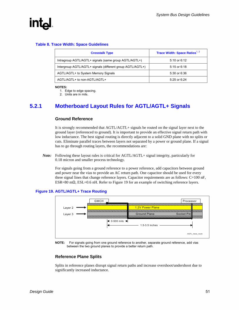
System Bus Design Guidelines
R
Design Guide 51
Table 8. Trace Width: Space Guidelines
Crosstalk Type Trace Width: Space Ratios1, 2
Intragroup AGTL/AGTL+ signals (same group AGTL/AGTL+) 5:10 or 6:12
Intergroup AGTL/AGTL+ signals (different group AGTL/AGTL+) 5:15 or 6:18
AGTL/AGTL+ to System Memory Signals 5:30 or 6:36
AGTL/AGTL+ to non-AGTL/AGTL+ 5:25 or 6:24
NOTES: 1. Edge to edge spacing. 2. Units are in mils.
5.2.1 Motherboard Layout Rules for AGTL/AGTL+ Signals
Ground Reference
It is strongly recommended that AGTL/AGTL+ signals be routed on the signal layer next to the ground layer (referenced to ground). It is important to provide an effective signal return path with low inductance. The best signal routing is directly adjacent to a solid GND plane with no splits or cuts. Eliminate parallel traces between layers not separated by a power or ground plane. If a signal has to go through routing layers, the recommendations are:
Note: Following these layout rules is critical for AGTL/AGTL+ signal integrity, particularly for 0.18 micron and smaller process technology.
For signals going from a ground reference to a power reference, add capacitors between ground and power near the vias to provide an AC return path. One capacitor should be used for every three signal lines that change reference layers. Capacitor requirements are as follows: C=100 nF, ESR=80 mΩ, ESL=0.6 nH. Refer to Figure 19 for an example of switching reference layers.
Figure 19. AGTL/AGTL+ Trace Routing
AGTL_trace_route
Ground Plane
1.2V Power Plane
GMCH Processor
Layer 2
Layer 3 Socket Pin
0-500 mils1.5-3.5 inches
NOTE: For signals going from one ground reference to another, separate ground reference, add vias between the two ground planes to provide a better return path.
Reference Plane Splits
Splits in reference planes disrupt signal return paths and increase overshoot/undershoot due to significantly increased inductance.

System Bus Design Guidelines
R
52 Design Guide
Processor Connector Breakout
It is strongly recommended that AGTL/AGTL+ signals do not traverse multiple signal layers. Intel recommends breaking out all signals from the connector on the same layer. If routing is tight, break out from the connector on the opposite routing layer over a ground reference and cross over to main signal layer near the processor connector.
Minimizing Crosstalk
The following general rules minimize the impact of crosstalk in a high-speed AGTL/AGTL+ bus design:
• Maximize the space between traces. Wherever possible, maintain a minimum of 10 mils (assuming a 5-mil trace) between trace edges. It may be necessary to use tighter spacing when routing between component pins. When traces must be close and parallel to each other, minimize the distance that they are close together and maximize the distance between the sections when the spacing restrictions are relaxed.
• Avoid parallelism between signals on adjacent layers, if there is no AC reference plane between them. As a rule of thumb, route adjacent layers orthogonally.
• Since AGTL/AGTL+ is a low-signal-swing technology, it is important to isolate AGTL/AGTL+ signals from other signals by at least 25 mils. This will avoid coupling from signals that have larger voltage swings, such as 5 V PCI.
• AGTL/AGTL+ signals must be well isolated from system memory signals. AGTL/AGTL+ signal trace edges must be at least 30 mils from system memory trace edges within 100 mils of the ball of the 82810E2 GMCH.
• Select a board stack-up that minimizes the coupling between adjacent signals. Minimize the nominal characteristic impedance within the AGTL/AGTL+ specification. Minimizing the height of the trace from its reference plane, which minimizes crosstalk, can do this.
• Route AGTL/AGTL+ address, data, and control signals in separate groups to minimize crosstalk between groups. Keep at least 15 mils between each group of signals.
• Minimize the dielectric used in the system. This makes the traces closer to their reference plane and thus reduces the crosstalk magnitude.
• Minimize the dielectric process variation used in the PCB fabrication.
• Minimize the cross-sectional area of the traces. This can be done by means of narrower traces and/or by using thinner copper, but the trade-off for this smaller cross-sectional area is higher trace resistivity, which can reduce the falling-edge noise margin because of the I*R loss along the trace.

System Bus Design Guidelines
R
Design Guide 53
5.2.1.1 Motherboard Layout Rules for Non-AGTL/AGTL+ (CMOS) Signals
Table 9. Routing Guidelines for Non-AGTL/AGTL+ Signals
Signal Trace Width Spacing to Other Traces Trace Length
A20M# 5 mils 10 mils 1 to 9
FERR# 5 mils 10 mils 1 to 9
FLUSH# 5 mils 10 mils 1 to 9
IERR# 5 mils 10 mils 1 to 9
IGNNE# 5 mils 10 mils 1 to 9
INIT# 5 mils 10 mils 1 to 9
LINT[0] (INTR) 5 mils 10 mils 1 to 9
LINT[1] (NMI) 5 mils 10 mils 1 to 9
PICD[1:0] 5 mils 10 mils 1 to 9
PREQ# 5 mils 10 mils 1 to 9
PWRGOOD 5 mils 10 mils 1 to 9
SLP# 5 mils 10 mils 1 to 9
SMI# 5 mils 10 mils 1 to 9
STPCLK 5 mils 10 mils 1 to 9
THERMTRIP# 5 mils 10 mils 1 to 9
NOTES: 1. Route these signals on any layer or combination of layers.
5.2.1.2 THRMDP and THRMDN
These traces (THRMDP and THRMDN) route the processor’s thermal diode connections. The thermal diode operates at very low currents and may be susceptible to crosstalk. The traces should be routed close together to reduce loop area and inductance.
Figure 20. Routing for THRMDP and THRMDN
1 Maximize (min. 20 mils)
1 Maximize (min. 20 mils)
2 Minimize
Signal Y
THRMDP
THRMDN
Signal Z bus_routing_thrmdp-thrmdn
NOTES: 1. Route these traces parallel and equalize lengths within ± 0.5 inch. 2. Route THRMDP and THRMDN on the same layer.

System Bus Design Guidelines
R
54 Design Guide
5.2.1.3 Additional Routing and Placement Considerations • Distribute VTT with a wide trace. A 0.050 inch minimum trace is recommended to minimize
DC losses. Route the VTT trace to all components on the host bus. Be sure to include decoupling capacitors.
• The VTT voltage should be 1.5 V ± 3% for static conditions, and 1.5 V ± 9% for worst-case transient conditions when a Pentium III processor (CPUID=068xh) or Celeron processor (CPUID=068xh) processor are present in the socket. If a future 0.13 micron socket 370 processor is being used, the VTT voltage should then be 1.25 V ± 3% for static conditions, and 1.25 V ± 9% for worst-case transient conditions.
• Place resistor divider pairs for VREF generation at the GMCH component. VREF also is delivered to the processor.
5.3 Electrical Differences for Universal PGA370 Designs There are several electrical changes between previous PGA370 designs and the universal PGA370 design, as follows:
• Changes to the PGA370 socket pin definitions.
• Addition of VTTPWRGD signal to ensure stable VID selection for future 0.13 micron socket 370 processors.
• Addition of THERMTRIP circuit to allow processor to detect catastrophic overheat.
• Addition of VID[25mV] signal to support future 0.13 micron socket 370 processors.
• Processor VTT level is switchable to 1.25V or 1.5V, depending on which processor is present in the socket.
• In designs using future 0.13 micron socket 370 processors, the processor does not generate VCMOS_REF.

System Bus Design Guidelines
R
Design Guide 55
5.3.1 THERMTRIP Circuit
Figure 21. Example Implementation of THERMTRIP Circuit
1.5V
Thermtrip#
SW _ON#
1 KΩ
4.7 KΩ
1 KΩ
1 KΩ
Thermstrip_2
1.8V
2.2 KΩ
CPU_RST#
Q1
Q2
Q3
NOTES: 1. The pull-up voltage on the collector of Q1 is required to be 1.8V derived from a 3.3V source. 2. THERMTRIP is not valid until after CPU_RST# is deasserted. This is handled by gating the assertion of
THERMTRIP with CPU_RST#. Using the CPU_RST# in this manner has minimal impact to the signal quality.
3. THERMTRIP must not go higher than VCCCMOS levels. The pull-up on THERMTRIP is now connected to 1.5V.
4. CPU_RST# must gate SW_ON# from ground. This prevents glitching on SW_ON# during power-up and powerdown.
5. The resistance to the base of the transistor gating CPU_RST# must be at least 2.2 kΩ for proper Vih levels on CPU_RST#.
5.3.1.1 THERMTRIP Timing
When the THERMTRIP signal is asserted, both the VCC and VTT supplies to the processor must be turned off to prevent thermal runaway of the processor. The time required from THERMTRIP asserted to VCC rail at ½ nominal is 500ms and THERMTRIP asserted to VTT rail at ½ nominal is 500ms. System designers must ensure that the decoupling scheme used on these rails does not violate the THERMTRIP timing specifications.
5.3.1.2 Workaround for THERMTRIP on 0.13 Micron Processors with CPUID=6B1h
A platform supporting the future 0.13 micron socket 370 processors must implement a workaround required for the future 0.13 micron socket 370 processor with a CPUID = 06B1h. The internal control register bit responsible for operation of the THERMTRIP circuit functionality may power up in an uninitialized state. As a result, THERMTRIP# may be incorrectly asserted during deassertion of RESET# at nominal operating temperatures. When THERMTRIP# is asserted as a result of this situation, the processor may shut down internally and stop execution. In addition, when the THERMTRIP# pin is asserted, the processor may incorrectly continue to execute, leading to intermittent system power-on boot failures. The occurrence and repeatability of failures is system dependent; however, all systems and processors are susceptible to failure.

System Bus Design Guidelines
R
56 Design Guide
To prevent the risk of power-on boot failures, a platform workaround is required. The system must provide a rising edge on the TCK signal during the power-on sequence that meets all of the following requirements:
• •Rising edge occurs after VCCCORE is valid and stable
• •Rising edge occurs before or at the deassertion of RESET#
• •Rising edge occurs after all VREF input signals are at valid voltage levels
• •TCK input meets the Vih min (1.3V) and max (1.65V) specification requirements
Specific workaround implementations may be platform specific. The following examples have been tested as acceptable workaround implementations.
The example workaround circuits (see Figure 22) attached require circuit modification for ITP tools to function correctly. These modifications must remove the workaround circuitry from the platform and may cause systems to fail to boot. Review the accompanying notes with each workaround for ITP modification details. If the system fails to boot when using ITP, issuing the ITP ‘Reset Target’ command on failing systems will reset the system and provide a sufficient rising edge on the TCK pin to ensure proper system boot.
In addition, the example workaround circuits shown do not support production motherboard test methodologies that require the use of the processor JTAG/TAP port. Alternative workaround solutions must be found if such test capability is required.
Figure 22. Example Circuit Showing ITP Workaround
TCK
PW RGD
39 ohmR5
R1
R2
R3
R4
0 ohm
330 ohm
510 ohm
1.3K ohm
TCK
PGA370
ITP
2.5V
ITP_exa
NOTES: 1. For Production Boards: Depopulate R5 2. To use ITP: Install R5, Depopulate R4
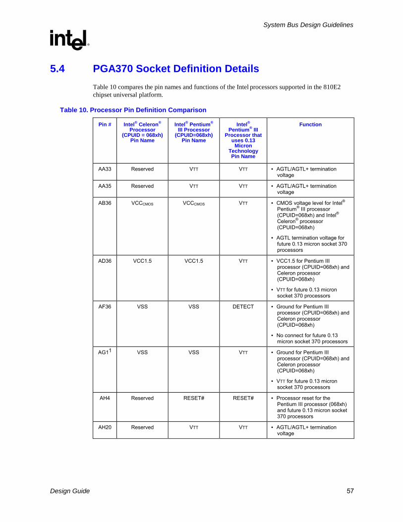
System Bus Design Guidelines
R
Design Guide 57
5.4 PGA370 Socket Definition Details Table 10 compares the pin names and functions of the Intel processors supported in the 810E2 chipset universal platform.
Table 10. Processor Pin Definition Comparison
Pin # Intel® Celeron® Processor
(CPUID = 068xh) Pin Name
Intel® Pentium® III Processor
(CPUID=068xh) Pin Name
Intel® Pentium® III
Processor that uses 0.13
Micron Technology Pin Name
Function
AA33 Reserved VTT VTT • AGTL/AGTL+ termination voltage
AA35 Reserved VTT VTT • AGTL/AGTL+ termination voltage
AB36 VCCCMOS VCCCMOS VTT • CMOS voltage level for Intel®
Pentium® III processor (CPUID=068xh) and Intel® Celeron® processor (CPUID=068xh)
• AGTL termination voltage for future 0.13 micron socket 370 processors
AD36 VCC1.5 VCC1.5 VTT • VCC1.5 for Pentium III processor (CPUID=068xh) and Celeron processor (CPUID=068xh)
• VTT for future 0.13 micron socket 370 processors
AF36 VSS VSS DETECT • Ground for Pentium III processor (CPUID=068xh) and Celeron processor (CPUID=068xh)
• No connect for future 0.13 micron socket 370 processors
AG11 VSS VSS VTT • Ground for Pentium III processor (CPUID=068xh) and Celeron processor (CPUID=068xh)
• VTT for future 0.13 micron socket 370 processors
AH4 Reserved RESET# RESET# • Processor reset for the Pentium III processor (068xh) and future 0.13 micron socket 370 processors
AH20 Reserved VTT VTT • AGTL/AGTL+ termination voltage

System Bus Design Guidelines
R
58 Design Guide
Pin # Intel® Celeron® Processor
(CPUID = 068xh) Pin Name
Intel® Pentium® III Processor
(CPUID=068xh) Pin Name
Intel® Pentium® III
Processor that uses 0.13
Micron Technology Pin Name
Function
AJ31 VSS VSS RESET2# • Ground for Pentium III processor (CPUID=068xh) and Celeron processor (CPUID=068xh)
• RESET for future 0.13 micron socket 370 processors
AK4 VSS VSS VTTPWRGD • Ground for Pentium III processor (CPUID=068xh) and Celeron processor (CPUID=068xh)
• VID control signal on future 0.13 micron socket 370 processors
AK16 Reserved VTT VTT • AGTL/AGTL+ termination voltage
AK22 GTL_REF GTL_REF VCMOS_REF • GTL reference voltage for Pentium III processor (CPUID=068xh) and Celeron processor (CPUID=068xh)
• CMOS reference voltage future 0.13 micron socket 370 processors
AK36 VSS VSS VID[25mV] • Ground for Pentium III processor (CPUID=068xh) and Celeron processor (CPUID=068xh)
• 25mV step VID select bit for future 0.13 micron socket 370 processors
AL13 Reserved VTT VTT • AGTL/AGTL+ termination voltage
AL21 Reserved VTT VTT • AGTL/AGTL+ termination voltage
AN3 GND GND DYN_OE • Ground for Pentium III processor (CPUID=068xh) and Celeron processor (CPUID=068xh)
• Dynamic output enable for future 0.13 micron socket 370 processors
AN11 Reserved VTT VTT • AGTL/AGTL+ termination voltage
AN15 Reserved VTT VTT • AGTL/AGTL+ termination voltage
AN21 Reserved VTT VTT • AGTL/AGTL+ termination voltage

System Bus Design Guidelines
R
Design Guide 59
Pin # Intel® Celeron® Processor
(CPUID = 068xh) Pin Name
Intel® Pentium® III Processor
(CPUID=068xh) Pin Name
Intel® Pentium® III
Processor that uses 0.13
Micron Technology Pin Name
Function
E23 Reserved VTT VTT • AGTL/AGTL+ termination voltage
G35 Reserved VTT VTT • AGTL/AGTL+ termination voltage
G37 Reserved Reserved VTT • Reserved for Pentium III processor (CPUID=068xh) and Celeron processor (CPUID=068xh)
• AGTL termination voltage for future 0.13 micron socket 370 processors
N37 NC NC NCHCTRL • No connect for Pentium III processor (CPUID=068xh) and Celeron processor (CPUID=068xh)
• NCHCTRL for future 0.13 micron socket 370 processors
S33 Reserved VTT VTT • AGTL/AGTL+ termination voltage
S37 Reserved VTT VTT • AGTL/AGTL+ termination voltage
U35 Reserved VTT VTT • AGTL/AGTL+ termination voltage
U37 Reserved VTT VTT • AGTL/AGTL+ termination voltage
W3 Reserved A34# A34# • Additional AGTL/AGTL+ address
X41 RESET# RESET2# VSS • Processor reset Pentium III processor (CPUID=068xh) and Celeron processor
• Ground for future 0.13 micron socket 370 processors
X6 Reserved A32# A32# • Additional AGTL/AGTL+ address
X34 VCCCORE VCCCORE VTT • Reserved for Pentium III processor (CPUID=068xh) and Celeron processor (CPUID=068xh)
• AGTL termination voltage for future 0.13 micron socket 370 processors

System Bus Design Guidelines
R
60 Design Guide
Pin # Intel® Celeron® Processor
(CPUID = 068xh) Pin Name
Intel® Pentium® III Processor
(CPUID=068xh) Pin Name
Intel® Pentium® III
Processor that uses 0.13
Micron Technology Pin Name
Function
Y1 Reserved Reserved Reserved • Reserved for Pentium III processor (CPUID=068xh) and Celeron processor (CPUID=068xh)
• No connect for future 0.13 micron socket 370 processors
Y33 Reserved CLKREF CLKREF • 1.25 V PLL reference
Z36 VCC2.5 VCC2.5 Reserved • VCC2.5 for Pentium III processor (CPUID=068xh) and Celeron processor (CPUID=068xh)
• No connect for future 0.13 micron socket 370 processors
NOTES: 1. Refer to Chapter 4.
5.5 BSEL[1:0] Implementation Differences Future 0.13 micron socket 370 processors will select the 133 MHz system bus frequency setting from the clock synthesizer. A Pentium III processor (CPUID=068xh) utilizes the BSEL1 pin to select either the 100 MHz or 133 MHz system bus frequency setting from the clock synthesizer. An Celeron processor (CPUID=068xh) uses both BSEL pins to select 66 MHz system bus frequency from the clock synthesizer. Processors in a FC-PGA or a FC-PGA2 are 3.3 V tolerant for these signals, as are the clock and chipset.
CK810 has been designed to support selections of 66 MHz, 100 MHz, and 133 MHz. The REF input pin has been redefined to be a frequency selection strap (BSEL1) during power-on and then becomes a 14 MHz reference clock output. Figure 23 shows the new BSEL[1:0] circuit design for universal PGA370 designs. Note that BSEL[1:0] now are pulled up using 1 kΩ resistors. Also refer to Figure 24 for more details.
Note: In a design supporting future 0.13 micron socket 370 processors, the BSEL[1:0] lines are not valid until VTTPWRGD is asserted. Refer to Section 4.2.10 for full details.

System Bus Design Guidelines
R
Design Guide 61
Figure 23. BSEL[1:0] Circuit Implementation for PGA370 Designs
Processor
BSEL0 BSEL1
GMCH
CK810E
1 kΩ1 kΩ
3.3V
BSEL_PGA370
3.3V
10 kΩ 10 kΩ
10 kΩ(Note 1)
REF
SEL0 SEL1
3.3V
8.2 kΩ
14 MHz REFCLK
Notes:1. If CLK810E is installed (66/100 MHz only), this resistor should not be stuffed.
5.6 CLKREF Circuit Implementation The CLKREF input, utilized by the Pentium III processor (CPUID=068xh) / Celeron processor (CPUID=068xh) and future 0.13 micron socket 370 processors, require a 1.25V source. It can be generated from a voltage divider on the VCC2.5 or VCC3.3 sources utilizing 1% tolerant resistors. A 4.7 µF decoupling capacitor should be included on this input. See Figure 24 and Table 11 for example CLKREF circuits.
Note: Do not use VTT as the source for this reference!
Figure 24. Examples for CLKREF Divider Circuit
VCC2.5
150 Ω 1%
150 Ω 1%
PGA370
CLKREF
Y33
4.7 µF
VCC3.3
R1
R2
PGA370
CLKREF
Y33
4.7 µF
sys_bus_CLKREF_divider

System Bus Design Guidelines
R
62 Design Guide
Table 11. Resistor Values for CLKREF Divider (3.3 V Source)
R1 (ΩΩΩΩ), 1% R2 (ΩΩΩΩ), 1% CLKREF Voltage (V)
182 110 1.243
301 182 1.243
374 221 1.226
499 301 1.242
5.7 Undershoot/Overshoot Requirements Undershoot and overshoot specifications become more critical as the process technology for microprocessors shrinks due to thinner gate oxide. Violating these undershoot and overshoot limits will degrade the life expectancy of the processor.
The Pentium III processor (CPUID=068xh) / Celeron processor (CPUID=068xh) and future 0.13 micron socket 370 processors have more restrictive overshoot and undershoot requirements for system bus signals than previous processors. These requirements stipulate that a signal at the output of the driver buffer and at the input of the receiver buffer must not exceed the maximum absolute overshoot voltage limit or the minimum absolute undershoot voltage limit. Exceeding either of these limits will damage the processor. There is also a time-dependent, non-linear overshoot and undershoot requirement that depends on the amplitude and duration of the overshoot/undershoot. See the appropriate processor’s electrical, mechanical and thermal specification for more details on the processor overshoot/undershoot specifications.

System Bus Design Guidelines
R
Design Guide 63
5.8 Processor Reset Requirements Universal PGA370 designs must route the AGTL/AGTL+ reset signal from the chipset to two pins on the processor as well as to the debug port connector. This reset signal is connected to the following pins at the PGA370 socket:
• AH4 (RESET#). The reset signal is connected to this pin for the Pentium III processor (CPUID=068xh), Celeron processor (CPUID=068xh), and future 0.13 micron socket 370 processors
• X4 (Reset2# or GND, depending on processor). The X4 pin is RESET2# for Pentium III processor (CPUID=068xh) and Celeron processor (CPUID=068xh). X4 is GND for future 0.13 micron socket 370 processors. An additional 1kΩ resistor is connected in series with pin X4 to the reset circuitry since pin X4 is a ground pin in future 0.13 micron socket 370 processors.
Note: The AGTL/AGTL+ reset signal must always terminate to VTT on the motherboard.
Designs that do not support the debug port will not utilize the 240 Ω series resistor or the connection of RESET# to the debug port connector. RESET2# is not required for platforms that do not support the Celeron processor (CPUID=068xh). Pin X4 should then be connected to ground.
The routing rules for the AGTL/AGTL+ reset signal are shown in Figure 25.
Figure 25. RESET#/RESET2# Routing Guidelines
ITP
Pin X4 Processor
Pin AH4
lenITP
VTT
Daisy chain
10 pF
86 Ω
lenCPUlenCS
91 Ω
cs_rtt_stub
Chipset
VTT
240 Ω
22 Ω
cpu_rtt_stub
sys_bus_reset_routin
1 kΩ
Table 12. RESET#/RESET2# Routing Guidelines (see Figure 25)
Parameter Minimum (in) Maximum (in)
LenCS 0.5 1.5
LenITP 1 3
LenCPU 0.5 1.5
cs_rtt_stub 0.5 1.5
cpu_rtt_stub 0.5 1.5

System Bus Design Guidelines
R
64 Design Guide
5.9 Processor PLL Filter Recommendations Intel PGA370 processors have internal phase lock loop (PLL) clock generators that are analog and require quiet power supplies to minimize jitter.
5.9.1 Topology
The general desired topology for these PLLs is shown in Figure 27. Not shown are the parasitic routing and local decoupling capacitors. Excluded from the external circuitry are parasitics associated with each component.
5.9.2 Filter Specification
The function of the filter is to protect the PLL from external noise through low-pass attenuation. The low-pass specification, with input at VCCCORE and output measured across the capacitor, is as follows:
• < 0.2 dB gain in pass band
• < 0.5 dB attenuation in pass band (see DC drop in next set of requirements)
• > 34 dB attenuation from 1 MHz to 66 MHz
• > 28 dB attenuation from 66 MHz to core frequency
The filter specification is graphically shown in Figure 26.

System Bus Design Guidelines
R
Design Guide 65
Figure 26. Filter Specification
0dB
-28dB
-34dB
0.2dB
-0.5 dB
1 MHz 66 MHz fcorefpeak1HzDC
passbandhigh frequency
band
filter_spec
ForbiddenZone
ForbiddenZone
NOTES: 1. Diagram not to scale. 2. No specification for frequencies beyond fcore. 3. fpeak should be less than 0.05 MHz.
Other requirements:
• Use shielded-type inductor to minimize magnetic pickup.
• Filter should support DC current > 30 mA.
• DC voltage drop from VCC to PLL1 should be < 60 mV, which in practice implies series R < 2 Ω. This also means pass-band (from DC to 1 Hz) attenuation < 0.5 dB for VCC = 1.1 V, and < 0.35 dB for VCC = 1.5 V.

System Bus Design Guidelines
R
66 Design Guide
5.9.3 Recommendation for Intel® Platforms
The following tables contain examples of components that meet Intel’s recommendations, when configured in the topology of Figure 27.
Table 13. Component Recommendations – Inductor
Part Number Value Tol. SRF Rated I DCR (Typical)
TDK MLF2012A4R7KT 4.7 µH 10% 35 MHz 30 mA 0.56 Ω (1 Ω max.)
Murata LQG21N4R7K00T1 4.7 µH 10% 47 MHz 30 mA 0.7 Ω (± 50%)
Murata LQG21C4R7N00 4.7 µH 30% 35 MHz 30 mA 0.3 Ω max.
Table 14. Component Recommendations – Capacitor
Part Number Value Tolerance ESL ESR
Kemet T495D336M016AS 33 µF
20% 2.5 nH 0.225 Ω
AVX TPSD336M020S0200 33 µF
20% 2.5 nH 0.2 Ω
Table 15. Component Recommendation – Resistor
Value Tolerance Power Note
1 Ω 10% 1/16 W
Resistor may be implemented with trace resistance, in which case a discrete R is not needed. See Figure 28.
To satisfy damping requirements, total series resistance in the filter (from VCCCORE to the top plate of the capacitor) must be at least 0.35 Ω. This resistor can be in the form of a discrete component or routing or both. For example, if the chosen inductor has minimum DCR of 0.25 Ω, then a routing resistance of at least 0.10 Ω is required. Be careful not to exceed the maximum resistance rule (2 Ω). For example, if using discrete R1 (1 Ω ± 1%), the maximum DCR of the L (trace plus inductor) should be less than 2.0 - 1.1 = 0.9 Ω, which precludes the use of some inductors and sets a max. trace length.
Other routing requirements:
• The capacitor (C) should be close to the PLL1 and PLL2 pins, < 0.1 Ω per route. These routes do not count towards the minimum damping R requirement.
• The PLL2 route should be parallel and next to the PLL1 route (i.e., minimize loop area).
• The inductor (L) should be close to C. Any routing resistance should be inserted between VCCCORE and L.
• Any discrete resistor (R) should be inserted between VCCCORE and L.

System Bus Design Guidelines
R
Design Guide 67
Figure 27. Example PLL Filter Using a Discrete Resistor
Processor
PLL1
PLL2
C
LR
VCCCORE
PLL_filter_1
Discrete resistor
<0.1 Ω route
<0.1 Ω route
Figure 28. Example PLL Filter Using a Buried Resistor
Processor
PLL1
PLL2
C
LR
VCCCORE
PLL_filter_2
Trace resistance
<0.1 Ω route
<0.1 Ω route

System Bus Design Guidelines
R
68 Design Guide
5.9.4 Custom Solutions
As long as designers satisfy filter performance and requirements as specified and outlined in Section 5.9.2, other solutions are acceptable. Custom solutions should be simulated against a standard reference core model, which is shown in Figure 29.
Figure 29. Core Reference Model
PLL1
PLL2
sys_bus_core_ref_model
0.1 Ω
0.1 Ω
120 pF 1 kΩ
Processor
NOTES: 1. 0.1 Ω resistors represent package routing. 2. 120 pF capacitor represents internal decoupling capacitor. 3. 1 kΩ resistor represents small signal PLL resistance. 4. Be sure to include all component and routing parasitics. 5. Sweep across component/parasitic tolerances. 6. To observe IR drop, use DC current of 30 mA and minimum VCCCORE level. 7. For other modules (interposer, DMM, etc.), adjust routing resistor if desired, but use minimum numbers.
5.10 Voltage Regulation Guidelines A universal PGA370 design will need the voltage regulation module (VRM) or on-board voltage regulator (VR) to be compliant with Intel VRM 8.5 DC-DC Converter Design Guidelines.

System Bus Design Guidelines
R
Design Guide 69
5.11 Decoupling Guidelines for Universal PGA370 Designs These preliminary decoupling guidelines for universal PGA370 designs are estimated to meet the specifications of VRM 8.5 DC-DC Converter Design Guidelines.
5.11.1 VCCCORE Decoupling Design • Sixteen or more 4.7 µF capacitors in 1206 packages.
All capacitors should be placed within the PGA370 socket cavity and mounted on the primary side of the motherboard. The capacitors are arranged to minimize the overall inductance between the VCCCORE/VSS power pins, as shown in Figure 30.
Figure 30. Capacitor Placement on the Motherboard
5.11.2 VTT Decoupling Design
For Itt = 2.3 A (max.)
• 20 0.1 µF capacitors in 0603 packages placed as closed as possible to the processor VTT pins. The capacitors are shown on the exterior of Figure 30.
5.11.3 VREF Decoupling Design • Four 0.1 µF capacitors in 0603 package placed near VREF pins (within 500 mils).

System Bus Design Guidelines
R
70 Design Guide
5.12 Thermal Considerations
5.12.1 Heatsink Volumetric Keep-Out Regions
Current heatsink recommendations are only valid for supported Celeron and Pentium III processor frequencies.
Figure 31 shows the system component keep-out volume above the socket connector required for the reference design thermal solution for high frequency processors. This keep-out envelope provides adequate room for the heatsink, fan and attach hardware under static conditions as well as room for installation of these components on the socket. The heatsink must be compatible with the Integrated Heat Spreader (IHS) used by higher frequency Pentium III processors.
Figure 32 shows component keep-outs on the motherboard required to prevent interference with the reference design thermal solution. Note portions of the heatsink and attach hardware hang over the motherboard.
Adhering to these keep-out areas will ensure compatibility with Intel boxed processor products and Intel enabled third party vendor thermal solutions for high frequency processors. While the keep-out requirements should provide adequate space for the reference design thermal solution, systems integrators should check with their vendors to ensure their specific thermal solutions fit within their specific system designs. Ensure that the thermal solutions under analysis comprehend the specific thermal design requirements for higher frequency Pentium III processors.
While thermal solutions for lower frequency processors may not require the full keep-out area, larger thermal solutions will be required for higher frequency processors, and failure to adhere to the guidelines will result in mechanical interference.
Figure 31. Heatsink Volumetric Keep-Out Regions

System Bus Design Guidelines
R
Design Guide 71
Figure 32. Motherboard Component Keep-Out Regions

System Bus Design Guidelines
R
72 Design Guide
5.13 Debug Port Changes Due to the lower voltage technology employed with newer processors, changes are required to support the debug port. Previously, test access port (TAP) signals used 2.5 V logic, as is the case with the Celeron processor in the PPGA package. Pentium III processor (CPUID=068xh) / Celeron processor (CPUID=068xh) and future 0.13 micron socket 370 processors utilize 1.5 V logic levels on the TAP. As a result, the type of debug port connecter used in universal PGA370 designs is dependent on the processor that is currently in the socket. The 1.5 V connector is a mirror image of the older 2.5 V connector. Either connector will fit into the same printed circuit board layout. Only the pin numbers would change (see Figure 33). Also required, along with the new connector, is an In-Target Probe* (ITP) that is capable of communicating with the TAP at the appropriate logic levels.
Figure 33. TAP Connector Comparison
2 4 6 8 10 12 14 16 18 20 22 24 26 28 30
1 3 5 7 9 11 13 15 17 19 21 23 25 27 29
1 3 5 7 9 11 13 15 17 19 21 23 25 27 29
2 4 6 8 10 12 14 16 18 20 22 24 26 28 30
RESET#
RESET#
2.5 V connector, AMP 104068-3 vertical plug, top view
1.5 V connector, AMP 104078-4 vertical receptacle, top view
sys_bus_TAP_conn
Caution: Pentium III processor (CPUID=068xh) and Celeron processor (CPUID=068xh) require an in-target probe (ITP) compatible with 1.5 V signal levels on the TAP. Previous ITPs were designed to work with higher voltages and may damage the processor if connected to any of these specified processors.
See the processor datasheet for more information regarding the debug port.
Layout and Routing Guidelines
R
Design Guide 73
6 Layout and Routing Guidelines This chapter describes motherboard layout and routing guidelines for Intel 810ET2 chipset systems, except for the processor layout guidelines. For the PGA370 processor-specific layout guidelines (Refer to Chapter 4). This chapter does not discuss the functional aspects of any bus or the layout guidelines for an add-in device.
Note: If the guidelines listed in this document are not followed, it is very important that thorough signal integrity and timing simulations are completed for each design. Even when the guidelines are followed, critical signals are recommended to be simulated to ensure proper signal integrity and flight time. Any deviation from these guidelines should be simulated.
6.1 General Recommendations The trace impedance typically noted (i.e., 60 Ω ±15%) is the “nominal” trace impedance for a 5 mil wide trace (i.e., the impedance of the trace when not subjected to the fields created by changing current in neighboring traces). When calculating flight times, it is important to consider the minimum and maximum impedance of a trace based on the switching of neighboring traces. Using wider spaces between the traces can minimize this trace-to-trace coupling. In addition, these wider spaces reduce settling time.
Coupling between two traces is a function of the coupled length, the distance separating the traces, the signal edge rate, and the degree of mutual capacitance and inductance. To minimize the effects of trace-to-trace coupling, the routing guidelines documented in this chapter should be followed.
Additionally, these routing guidelines are created using the stack-up (refer to Figure 34). If this stack-up is not used, simulations should be completed.

Layout and Routing Guidelines
R
74 Design Guide
6.2 Nominal Board Stack-Up The Intel 810E2 chipset for use with universal socket 370 platform requires a board stack-up yielding a target impedance of 60 Ω ±15% with a 5 mil nominal trace width. Figure 34 presents an example stack-up to achieve this. It is a 4-layer fabrication construction using 53% resin, FR4 material.
Figure 34. Nominal Board Stack-Up
Component Side Layer 1 (1/2 oz. cu)
Power Plane Layer 2 (1 oz. cu)
Ground Layer 3 (1 oz. cu)
Solder SIde Layer 4 (1/2 oz. cu)
4.5 mil Prepreg
4.5 mil Prepreg
~48 mil Core
62 milsTotal
Thickness
stackup.vsd
6.3 System Memory Layout Guidelines
6.3.1 System Memory Solution Space
Figure 35. System Memory Topologies
F
G
G
DIMM0 DIMM1
Topology 1
Topology 2
Topology 3
Topology 4
Topology 5
GMCH
A B10 ohm
A C10 ohm
A D
A D
A E

Layout and Routing Guidelines
R
Design Guide 75
Table 16. System Memory Routing
Trace Lengths (inches)
Trace (mils) A B C D E F G
Signal Top. Width Space Max Min Max Min Max Min Max Min Max Min Max Min Max
SCS[3:2]# Opt.1 5 10 8 3 5 1.5 2
Opt.2 5 10 8 2.2 5 1.5 1.8
Opt.3 5 10 8 1.6 5 1.15 1.5
SCS[1:0]# Opt.1 4 10 8 3 5 1.5 2
Opt.2 4 10 8 2.2 5 1.5 1.8
Opt.3 4 10 8 1.6 5 1.15 1.5
SMAA[7:4] 1 10 8 0.5 0.5 2
SMAB[7:4]# 2 10 8 0.5 0.5 2
SCKE[1:0] 3 10 8 1 2.5 0.4 1
SMD[63:0], SDQM[7:0]
3 5 7 1 3 0.4 1
SCAS#, SRAS#, SWE#
3 5 7 1 3.5 0.4 1
SBS[1:0], SMAA[11:8, 3:0]
3 5 7 1 2.5 0.4 1
NOTES: 1. It is recommended to add 10 Ω series resistors to the MAA[7:4] and the MAB[7:4] lines, as close as
possible to GMCH for signal integrity.

Layout and Routing Guidelines
R
76 Design Guide
6.3.2 System Memory Routing Example
Figure 36. System Memory Routing Example
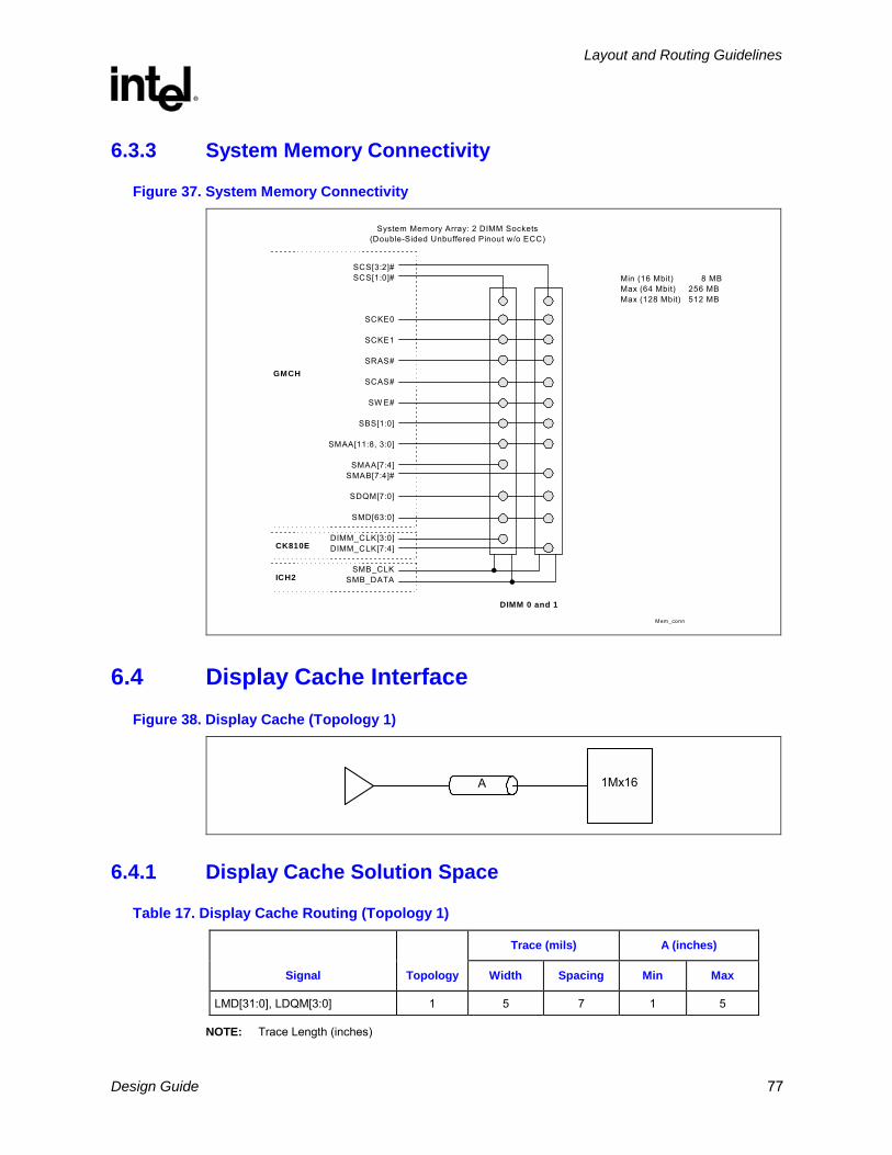
Layout and Routing Guidelines
R
Design Guide 77
6.3.3 System Memory Connectivity
Figure 37. System Memory Connectivity
SCS[3:2]#SCS[1:0]#
SCKE0
SCKE1
SRAS#
SCAS#
SW E#
SBS[1:0]
SMAA[11:8, 3:0]
SMAA[7:4]SMAB[7:4]#
SDQM[7:0]
SMD[63:0]
DIMM_CLK[3:0]DIMM_CLK[7:4]
SMB_CLKSMB_DATA
System Memory Array: 2 DIMM Sockets(Double-Sided Unbuffered Pinout w/o ECC)
GMCH
CK810E
ICH2
DIMM 0 and 1
Mem_conn
Min (16 Mbit) 8 MBMax (64 Mbit) 256 MBMax (128 Mbit) 512 MB
6.4 Display Cache Interface Figure 38. Display Cache (Topology 1)
A 1Mx16
6.4.1 Display Cache Solution Space
Table 17. Display Cache Routing (Topology 1)
Trace (mils) A (inches)
Signal Topology Width Spacing Min Max
LMD[31:0], LDQM[3:0] 1 5 7 1 5
NOTE: Trace Length (inches)

Layout and Routing Guidelines
R
78 Design Guide
Figure 39. Display Cache (Topology 2)
1Mx16
1Mx16
B
C
C
Table 18. Display Cache Routing (Topology 2)
Trace (units=mils) B (inches) C (inches)
Signal Topology Width Spacing Min Max Min Max
LMA[11:0], LWE#, LCS#, LRAS#, LCAS# 2 5 7 1 3.75 0.75 1.25
Figure 40. Display Cache (Topology 3)
1Mx16
1Mx16
D E
F
F
22 Ohms
Table 19. Display Cache Routing (Topology 3)
Trace (units=mils) D (inches) E (inches) F (inches)
Signal Topology Width Spacing Length Min Max Min Max
TCLK 3 5 7 0.5 1.5 2.5 0.75 1.25
Figure 41. Display Cache (Topology 4)
G H33 Ohms
OCLK
RCLK

Layout and Routing Guidelines
R
Design Guide 79
Table 20. Display Cache Routing (Topology 4)
Trace (units=mils) G (inches) H (inches)
Signal Topology Width Spacing Length Min Max
OCLK 4 5 6 0.5 3.25 3.75
6.5 Hub Interface The 810ET2 chipset’s GMCH ball assignment and ICH2 ball assignment have been optimized to simplify hub interface routing. It is recommended that the hub interface signals be routed directly from the GMCH to the ICH2 on the top signal layer. Refer to Figure 42.
The hub interface is divided into two signal groups: data signals and strobe signals.
• Data Signals: HL[10:0]
• Strobe Signals: HL_STB HL_STB#
Note: HL_STB/HL_STB# is a differential strobe pair.
No pull-ups or pull-downs are required on the hub interface. HL[11] on the ICH2 should be brought out to a test point for NAND Tree testing. Each signal should be routed such that it meets the guidelines documented for its signal group.
Figure 42. Hub Interface Signal Routing Example
ICH2 GMCH
Clocks
HL_STB
HL_STB#
HL[10:0]
CLK66 GCLK
HL11
hub_link_sig_routing
NAND treetest point
Layout and Routing Guidelines
R
80 Design Guide
6.5.1 Data Signals
Hub interface data signals should be routed with a trace width of 5 mils and a trace spacing of 20 mils. These signals can be routed with a trace width of 5 mils and a trace spacing of 15 mils for navigation around components or mounting holes. To break out of the GMCH and the ICH2, the hub interface data signals can be routed with a trace width of 5 mils and a trace spacing of 5 mils. The signals should be separated to a trace width of 5 mils and a trace spacing of 20 mils, within 0.3 inch of the GMCH/ICH2 components.
The maximum trace length for the hub interface data signals is 7 inches. These signals should each be matched within ±0.1 inch of the HL_STB and HL_STB# signals.
6.5.2 Strobe Signals
Due to their differential nature, the hub interface strobe signals should be 5 mils wide and routed 20 mils apart. This strobe pair should be a minimum of 20 mils from any adjacent signals. The maximum length for the strobe signals is 7 inches, and the two strobes should be the same length. Additionally, the trace length for each data signal should be matched to the trace length of the strobes, within ±0.1 inch.
6.5.3 HREF Generation/Distribution
HREF, the hub interface reference voltage, is 0.5 * 1.8 V = 0.9 V ± 2%. It can be generated using a single HREF divider or locally generated dividers (as shown in Figure 43 and Figure 44). The resistors should be equal in value and rated at 1% tolerance, to maintain 2% tolerance on 0.9 V. The values of these resistors must be chosen to ensure that the reference voltage tolerance is maintained over the entire input leakage specification. The recommended range for the resistor value is from a minimum of 100 Ω to a maximum of 1 kΩ (300 Ω shown in example).
The single HREF divider should not be located more than 4 inches away from either GMCH or ICH2. If the single HREF divider is located more than 4 inches away, then the locally generated hub interface reference dividers should be used instead.
The reference voltage generated by a single HREF divider should be bypassed to ground at each component with a 0.01 µF capacitor located close to the component HREF pin. If the reference voltage is generated locally, the bypass capacitor must be close to the component HREF pin.

Layout and Routing Guidelines
R
Design Guide 81
6.5.4 Compensation
Independent Hub interface compensation resistors are used by the 810ET2 chipset’s GMCH and the ICH2 to adjust buffer characteristics to specific board characteristics. Refer to the Intel® 810ET2 Chipset Family: 82810 Graphics and Memory Controller Hub (GMCH) Datasheet and the Intel® 82801BA I/O Controller Hub 2 (ICH2) and Intel® 82801 BAM I/O Controller Hub 2 Mobile (ICH2-M) Datasheet for details on compensation. The resistive Compensation (RCOMP) guidelines are as follows:
• RCOMP: Tie the HLCOMP pin of each component to a 40 Ω, 1% or 2% pull-up resistor (to 1.8 V) via a 10-mil-wide, 0.5 inch trace (targeted at a nominal trace impedance of 40 Ω). The GMCH and ICH2 each require their own RCOMP resistor.
Figure 43. Single Hub Interface Reference Divider Circuit
HUBREF HUBREF
GMCH ICH2
hub_IF_ref_div_1
300 Ω
1.8 V
300 Ω0.01 µF 0.01 µF
0.1 µF
Figure 44. Locally Generated Hub Interface Reference Dividers
HUBREF HUBREF
GMCH ICH2
hub_IF_ref_div_2
300 Ω
1.8 V
300 Ω 0.1 µF
300 Ω
1.8 V
300 Ω0.1 µF

Layout and Routing Guidelines
R
82 Design Guide
6.6 Intel® ICH2
6.6.1 Decoupling
The ICH2 is capable of generating large current swings when switching between logic High and logic Low. This condition could cause the component voltage rails to drop below specified limits. To avoid this type of situation, ensure that the appropriate amount of bulk capacitance is added in parallel to the voltage input pins. It is recommended that the developer use the amount of decoupling capacitors specified in Table 21 to ensure that the component maintains stable supply voltages. The capacitors should be placed as close as possible to the package, without exceeding 400 mils (100–300 mils nominal).
Note: Routing space around the ICH2 is tight. A few decoupling caps may be placed more than 300 mils away from the package. System designers should simulate the board to ensure that the correct amount decoupling is implemented. Refer to Figure 45 for a layout example. It is recommended that, for prototype board designs, the designer include pads for extra power plane decoupling caps.
Table 21. Decoupling Capacitor Recommendation
Power Plane/Pins Decoupling Capacitors Capacitor Value
3.3 V core 6 0.1 µF
3.3 V standby 1 0.1 µF
Processor interface (1.3 ~ 2.5 V) 1 0.1 µF
1.8 V core 2 0.1 µF
1.8 V standby 1 0.1 µF
5 V reference 1 0.1 µF
5 V reference standby 1 0.1 µF

Layout and Routing Guidelines
R
Design Guide 83
Figure 45. Intel® ICH2 Decoupling Capacitor Layout
3.3V Core1.8V Core
1.8V Standby
3.3V Standby
3.3V Core1.8V Standby
5V Refdecouple_cap_layout
6.7 1.8V/3.3V Power Sequencing The ICH2 has two pairs of associated 1.8V and 3.3V supplies. These are VCC1.8, VCC3.3 and VCCSus1_8, VCCSus3_3. These pairs are assumed to power up and power down together. The difference between the two associated supplies must never be greater than 2.0V. The 1.8V supply may come up before the 3.3V supply without violating this rule (though this is generally not practical in a desktop environment, since the 1.8V supply is typically derived from the 3.3V supply by means of a linear regulator).
One serious consequence of violation of this "2V Rule" is electrical overstress of oxide layers, resulting in component damage.
The majority of the ICH2 I/O buffers are driven by the 3.3V supplies, but are controlled by logic that is powered by the 1.8V supplies. Thus, another consequence of faulty power sequencing arises if the 3.3V supply comes up first. In this case the I/O buffers will be in an undefined state until the 1.8V logic is powered up. Some signals that are defined as "Input-only" actually have output buffers that are normally disabled, and the ICH2 may unexpectedly drive these signals if the 3.3V supply is active while the 1.8V supply is not.
Figure 46 shows an example power-on sequencing circuit that ensures the “2V Rule” is obeyed. This circuit uses a NPN (Q2) and PNP (Q1) transistor to ensure the 1.8V supply tracks the 3.3V supply. The NPN transistor controls the current through PNP from the 3.3V supply into the 1.8V power plane by varying the voltage at the base of the PNP transistor. By connecting the emitter of

Layout and Routing Guidelines
R
84 Design Guide
the NPN transistor to the 1.8V plane, current will not flow from the 3.3V supply into 1.8V plane when the 1.8V plane reaches 1.8V.
Figure 46. Example 1.8V/3.3V Power Sequencing Circuit
Q1 PNP
Q2 NPN
220
220
470
+3.3V +1.8V
When analyzing systems that may be "marginally compliant" to the 2V Rule, pay close attention to the behavior of the ICH2's RSMRST# and PWROK signals, since these signals control internal isolation logic between the various power planes:
• RSMRST# controls isolation between the RTC well and the resume wells.
• PWROK controls isolation between the resume wells and main wells
If one of these signals goes high while one of its associated power planes is active and the other is not, a leakage path will exist between the active and inactive power wells. This could result in high, possibly damaging, internal currents.

Layout and Routing Guidelines
R
Design Guide 85
6.8 Power Plane Splits Figure 47. Power Plane Split Example
pwr_plane_splits
6.9 Thermal Design Power The thermal design power is the estimated maximum possible expected power generated in a component by a realistic application. It is based on extrapolations in both hardware and software technology over the life of the product. It does not represent the expected power generated by a power virus.
The thermal design power for the ICH2 is 1.5 W ±15%.
6.10 IDE Interface This section contains guidelines for connecting and routing the ICH2 IDE interface. The ICH2 has two independent IDE channels. This section provides guidelines for IDE connector cabling and motherboard design, including component and resistor placement and signal termination for both IDE channels. The ICH2 has integrated the series resistors that typically have been required on the IDE data signals (PDD[15:0] and SDD[15:0]) running to the two ATA connectors. Intel does not anticipate requiring additional series termination, but OEMs should verify the motherboard signal integrity via simulation. Additional external 0 Ω resistors can be incorporated into the design to address possible noise issues on the motherboard. The additional resistor layout increases flexibility by providing future stuffing options.
Layout and Routing Guidelines
R
86 Design Guide
The IDE interface can be routed with 5-mil traces on 7-mil spaces and must be less than 8 inches long (from ICH2 to IDE connector). Additionally, the shortest IDE signal (on a given IDE channel) must be less than 0.5 inch shorter than the longest IDE signal (on that channel).
6.10.1 Cabling • Length of cable: Each IDE cable must be equal to or less than 18 inches.
• Capacitance: Less than 30 pF
• Placement: A maximum of 6 inches between drive connectors on the cable. If a single drive is placed on the cable, it should be placed at the end of the cable. If a second drive is placed on the same cable, it should be placed on the connector next closest to the end of the cable (6 inches away from the end of the cable).
• Grounding: Provide a direct, low-impedance chassis path between the motherboard ground and hard disk drives.
• ICH2 Placement: The ICH2 must be placed at most 8 inches from the ATA connector(s).
• PC99 Requirement: Support Cable Select for master-slave configuration is a system design requirement of Microsoft* PC99. The CSEL signal of each ATA connector must be grounded at the host side.
6.11 Cable Detection for Ultra ATA/66 and Ultra ATA/100 The ICH2 IDE controller supports PIO, multiword (Intel 8237-style) DMA, and Ultra DMA modes 0 through 5. The ICH2 must determine the type of cable present, to configure itself for the fastest possible transfer mode that the hardware can support.
An 80-conductor IDE cable is required for Ultra ATA/66 and Ultra ATA/100. This cable uses the same 40-pin connector as the old 40-pin IDE cable. The wires in the cable alternate: ground, signal, ground, signal. All ground wires are tied together on the cable (and they are tied to the ground on the motherboard through the ground pins in the 40-pin connector). This cable conforms to the Small Form Factor Specification SFF-8049, which is obtainable from the Small Form Factor Committee.
To determine whether the ATA/66 or ATA/100 mode can be enabled, the ICH2 requires that the system software attempt to determine the type of cable used in the system. If the system software detects an 80-conductor cable, it may use any Ultra DMA mode up to the highest transfer mode supported by both the chipset and the IDE device. If a 40-conductor cable is detected, the system software must not enable modes faster than Ultra DMA Mode 2 (Ultra ATA/33).
Intel recommends that cable detection be performed using a combination host-side/device-side detection mechanism. Note that host-side detection cannot be implemented on an NLX form factor system, since this configuration does not define interconnect pins for the PDIAG#/CBLID# from the riser (containing the ATA connectors) to the motherboard. These systems must rely on the device-side detection mechanism only.

Layout and Routing Guidelines
R
Design Guide 87
6.11.1 Combination Host-Side/Device-Side Cable Detection
Host-side detection (described in the ATA/ATAPI-4 Standard, Section 5.2.11) requires the use of two GPI pins (one for each IDE channel). The proper way to connect the PDIAG#/CBLID# signal of the IDE connector to the host is shown in Figure 48. All IDE devices have a 10 kΩ pull-up resistor to 5 volts on this signal. Not all GPI and GPIO pins on the ICH2 are 5-volt tolerant. If non 5-volt tolerant inputs are used, a resistor divider is required to prevent 5 V on the ICH2 or FWH pins. The proper value of the divider resistor is 10 kΩ (as shown in Figure 48).
Figure 48. Combination Host-Side / Device-Side IDE Cable Detection
80-conductorIDE cable
IDE drive
5 V
ICH2
GPIO
GPIO
Open
IDE drive
5 V
40-conductorcable
IDE drive
5 V
PDIAG#ICH2
GPIO
GPIO
IDE drive
5 V
Resistor required fornon-5V-tolerant GPI.
PDIAG#
PDIAG#PDIAG#
Resistor required fornon-5V-tolerant GPI.
10 kΩ
10 kΩ
To secondaryIDE connector
To secondaryIDE connector
PDIAG#/CBLID#
PDIAG#/CBLID#
10 kΩ
10 kΩ
10 kΩ
10 kΩ
IDE_combo_cable_det
This mechanism allows the BIOS, after diagnostics, to sample PDIAG#/CBLID#. If the signal is High, then there is a 40-conductor cable in the system and ATA modes 3, 4 and 5 must not be enabled.
If PDIAG#/CBLID# is detected Low, then there may be an 80-conductor cable in the system or there may be a 40-conductor cable and a legacy slave device (Device 1) that does not release the PDIAG#/CBLID# signal as required by the ATA/ATAPI-4 standard. In this case, the BIOS should check the Identify Device information in a connected device that supports Ultra DMA modes higher than 2. If ID Word 93, bit 13, is set to 1, then an 80-conductor cable is present. If this bit is set to 0, then a legacy slave (Device 1) is preventing proper cable detection, so the BIOS should configure the system as though a 40-conductor cable were present and then notify the user of the problem.

Layout and Routing Guidelines
R
88 Design Guide
6.11.2 Device-Side Cable Detection
For platforms that must implement device-side detection only (e.g., NLX platforms), a 0.047 µF capacitor is required on the motherboard as shown in Figure 49. This capacitor should not be populated when implementing the recommended combination host-side/device-side cable detection mechanism described previously.
Figure 49. Device-Side IDE Cable Detection
80-conductorIDE cable
IDE drive
5 V
ICH2
Open
IDE drive
5 V
40-conductorcable
IDE drive
5 V
PDIAG#ICH2
IDE drive
5 V
PDIAG#
PDIAG#PDIAG#PDIAG#/CBLID#
PDIAG#/CBLID#
10 kΩ
10 kΩ
10 kΩ
10 kΩ
IDE_dev_cable_det
0.047 µF
0.047 µF
This mechanism creates a resistor-capacitor (RC) time constant. The ATA mode 3, 4 or 5 drive will drive PDIAG#/CBLID# Low and then release it (pulled up through a 10 kΩ resistor). The drive will sample the signal after releasing it. In an 80-conductor cable, PDIAG#/CBLID# is not connected through to the host, so the capacitor has no effect. In a 40-conductor cable, the signal is connected to the host, so the signal will rise more slowly as the capacitor charges. The drive can detect the difference in rise times and will report the cable type to the BIOS when it sends the IDENTIFY_DEVICE packet during system boot, as described in the ATA/66 specification.

Layout and Routing Guidelines
R
Design Guide 89
6.11.3 Primary IDE Connector Requirements
Figure 50. Connection Requirements for Primary IDE Connector
PCIRST# *
PDD[15:0]
PDA[2:0]PDCS1#PDCS3#PDIOR#
PDIOW#PDDREQ
PIORDY
IRQ14
PDDACK#
GPIOx
ICH2
Primary IDEConnector
IDE_primary_conn_require
Reset#
PDIAG# / CBLID#
N.C. Pins 32 & 34
CSEL
* Due to ringing, PCIRST# must be buffered.
3.3 V3.3 V
4.7 kΩ 8.210 kΩ
10 kΩ(needed only for
non-5V-tolerant GPI)
2247 ΩPCIRST_BUF#
NOTES: 1. 22 Ω to 47 Ω series resistors are required on RESET#. The correct value should be determined for
each unique motherboard design, based on signal quality. 2. An 8.2 kΩ to 10 kΩ pull-up resistor is required on IRQ14 and IRQ15 to VCC3. 3. A 4.7 kΩ pull-up resistor to VCC3 is required on PIORDY and SIORDY. 4. Series resistors can be placed on the control and data lines to improve signal quality. The resistors are
placed as close as possible to the connector. Values are determined for each unique motherboard design.
5. The 10 kΩ resistor to ground on the PDIAG#/CBLID# signal is now required on the Primary Connector. This change is to prevent the GPI pin from floating if a device is not present on the IDE interface.
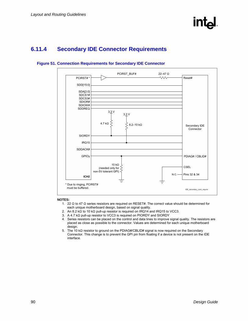
Layout and Routing Guidelines
R
90 Design Guide
6.11.4 Secondary IDE Connector Requirements
Figure 51. Connection Requirements for Secondary IDE Connector
PCIRST# *
SDD[15:0]
SDA[2:0]SDCS1#SDCS3#SDIOR#SDIOW#SDDREQ
SIORDY
IRQ15
SDDACK#
GPIOy
ICH2
Secondary IDEConnector
IDE_secondary_conn_require
Reset#
PDIAG# / CBLID#
N.C. Pins 32 & 34
CSEL
* Due to ringing, PCIRST# must be buffered.
3.3 V3.3 V
4.7 kΩ 8.210 kΩ
10 kΩ(needed only for
non-5V-tolerant GPI)
2247 ΩPCIRST_BUF#
NOTES: 1. 22 Ω to 47 Ω series resistors are required on RESET#. The correct value should be determined for
each unique motherboard design, based on signal quality. 2. An 8.2 kΩ to 10 kΩ pull-up resistor is required on IRQ14 and IRQ15 to VCC3. 3. A 4.7 kΩ pull-up resistor to VCC3 is required on PIORDY and SIORDY 4. Series resistors can be placed on the control and data lines to improve signal quality. The resistors are
placed as close as possible to the connector. Values are determined for each unique motherboard design.
5. The 10 kΩ resistor to ground on the PDIAG#/CBLID# signal is now required on the Secondary Connector. This change is to prevent the GPI pin from floating if a device is not present on the IDE interface.
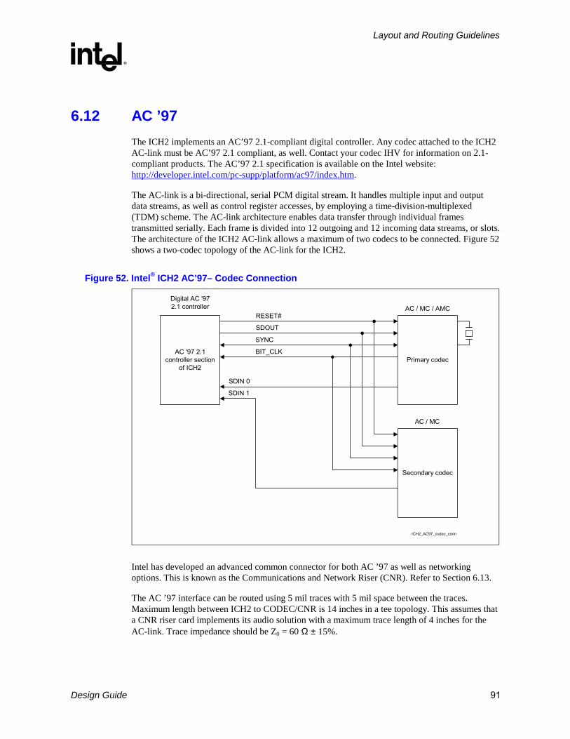
Layout and Routing Guidelines
R
Design Guide 91
6.12 AC ’97 The ICH2 implements an AC’97 2.1-compliant digital controller. Any codec attached to the ICH2 AC-link must be AC’97 2.1 compliant, as well. Contact your codec IHV for information on 2.1-compliant products. The AC’97 2.1 specification is available on the Intel website: http://developer.intel.com/pc-supp/platform/ac97/index.htm.
The AC-link is a bi-directional, serial PCM digital stream. It handles multiple input and output data streams, as well as control register accesses, by employing a time-division-multiplexed (TDM) scheme. The AC-link architecture enables data transfer through individual frames transmitted serially. Each frame is divided into 12 outgoing and 12 incoming data streams, or slots. The architecture of the ICH2 AC-link allows a maximum of two codecs to be connected. Figure 52 shows a two-codec topology of the AC-link for the ICH2.
Figure 52. Intel® ICH2 AC’97– Codec Connection
AC '97 2.1controller section
of ICH2
Digital AC '972.1 controller
Primary codec
Secondary codec
AC / MC
AC / MC / AMC
ICH2_AC97_codec_conn
SDIN 0
SDIN 1
RESET#
SDOUT
SYNC
BIT_CLK
Intel has developed an advanced common connector for both AC ’97 as well as networking options. This is known as the Communications and Network Riser (CNR). Refer to Section 6.13.
The AC ’97 interface can be routed using 5 mil traces with 5 mil space between the traces. Maximum length between ICH2 to CODEC/CNR is 14 inches in a tee topology. This assumes that a CNR riser card implements its audio solution with a maximum trace length of 4 inches for the AC-link. Trace impedance should be Z0 = 60 Ω ± 15%.

Layout and Routing Guidelines
R
92 Design Guide
Clocking is provided from the primary codec on the link via BITCLK, and it is derived from a 24.576 MHz crystal or oscillator. Refer to the primary codec vendor for crystal or oscillator requirements. BITCLK is a 12.288 MHz clock driven by the primary codec to the digital controller (ICH2) and any other codec present. That clock is used as the timebase for latching and driving data.
The ICH2 supports wake-on-ring from S1–S5 via the AC’97 link. The codec asserts SDATAIN to wake the system. To provide wake capability and/or caller ID, standby power must be provided to the modem codec.
ICH2 has weak pull-downs/pull-ups that are enabled only when the AC-Link Shut-off bit in the ICH2 is set. This keeps the link from floating when the AC-link is off or when there are no codecs present.
If the Shut-off bit is not set, it means that there is a codec on the link. Therefore, BITCLK and AC_SDOUT will be driven by the codec and ICH2, respectively. However, AC_SDIN0 and AC_SDIN1 may not be driven. If the link is enabled, it may be assumed that there is at least one codec. If there only is an on-board codec (i.e., no AMR), then the unused SDIN pin should have a weak (10 kΩ) pull-down to keep it from floating. If an AMR is used, any SDIN signal could be Not Connected (e.g., with no codec, both can be NC), then both SDIN pins must have a 10 kΩ pull-down.
Table 22. AC'97 SDIN Pull-Down Resistors
System Solution Pull-Up Requirements
On-board codec only Pull down the SDIN pin that is not connected to the codec.
AMR only Pull down both SDIN pins.
BOTH AMR and on-board codec Pull down any SDIN pin that could be NC1.
NOTES: 1. If the on-board codec can be disabled, both SDIN pins must have pull-downs. If the on-board codec
cannot be disabled, only the SDIN not connected to the on-board codec requires a pull-down.
6.12.1 AC’97 Audio Codec Detect Circuit and Configuration Options
The following provides general circuits to implement a number of different codec configurations. Refer to Intel’s White Paper Recommendations for ICHx/AC’97 Audio (Motherboard and Communication and Network Riser) for Intel’s recommended codec configurations.
To support more than two channels of audio output, the ICH2 allows for a configuration where two audio codecs work concurrently to provide surround capabilities. To maintain data-on-demand capabilities, the ICH2 AC’97 controller, when configured for 4 or 6 channels, will wait for all the appropriate slot request bits to be set before sending data in the SDATA_OUT slots. This allows for simple FIFO synchronization of the attached codecs. It is assumed that both codecs will be programmed to the same sample rate, and that the codecs have identical (or at least compatible) FIFO depth requirements. It is recommended that the codecs be provided by the same vendor, upon the certification of their interoperability in an audio channel configuration.
The following four circuit figures (Figure 53 to Figure 56)show the adaptability of a system with the modification of RA and RB combined with some basic glue logic to support multiple codec

Layout and Routing Guidelines
R
Design Guide 93
configurations. This also provides a mechanism to make sure that only two codecs are enabled in a given configuration and allows the configuration of the link to be determined by BIOS so that the correct PnP IDs can be loaded.
As shown in Figure 53, when a single codec is located on the motherboard, the resistor RA and the circuitry (AND and NOT gates) shown inside the dashed box must be implemented on the motherboard. This circuitry is required to disable the motherboard codec when a CNR is installed containing two AC ’97 codecs (or a single AC ’97 codec that must be the primary codec on the AC-Link).
By installing resistor RB (1 kΩ) on the CNR, the codec on the motherboard becomes disabled (held in reset) and the codec(s) on the CNR take control of the AC-Link. One possible example of using this architecture is a system integrator installing an audio plus modem CNR in a system already containing an audio codec on the motherboard. The audio codec on the motherboard would then be disabled, allowing all of the codecs on the CNR to be used.
Figure 53. CDC_DN_ENAB# Support Circuitry for a Single Codec on Motherboard
AC97_1
Codec A
RESET#
SDATA_IN
Codec C
RESET#
SDATA_INAC97_RESET#
Vcc
CDC_DN_ENAB#
CNR BoardMotherboard
RA
10kohms
RB
1kohmsTo General
Purpose Input
From AC '97Controller
CNR Connector
To AC '97
DigitalController
SDATA_IN0
SDATA_IN1
Codec D
RESET#
SDATA_IN
The architecture shown in Figure 54 has some unique features. These include the possibility of the CNR being used as an upgrade to the existing audio features of the motherboard (by simply changing the value of resistor RB on the CNR to 100 kΩ). An example of one such upgrade is increasing from two-channel to four or six-channel audio.
Both Figure 54 and Figure 55 show a switch on the CNR board. This is necessary to connect the CNR board codec to the proper SDATA_INn line so there is not a conflict with the motherboard codec(s).

Layout and Routing Guidelines
R
94 Design Guide
Figure 54. CDC_DN_ENAB# Support Circuitry for Multi-Channel Audio Upgrade
PrimaryAudioCodec
RESET#SDATA_IN
AudioCodecRESET#
ID0#SDATA_IN
AC97_RESET#
CDC_DN_ENAB#
CNR BoardMotherboard
RA10kohms
To GeneralPurpose Input
From AC '97Controller
CNR Connector
SDATA_IN0
SDATA_IN1To AC '97
DigitalController
Vcc
RB100kohms
Figure 55 shows the circuitry required on the motherboard to support a two-codec down configuration. This circuitry disables the codec on a single codec CNR. Notice that in this configuration the resistor RB has been changed to 100 kΩ.
Figure 55. CDC_DN_ENAB# Support Circuitry for Two-Codecs on Motherboard / One-Codec on CNR
PrimaryAudioCodec
RESET#SDATA_IN
AudioCodecRESET#
ID0#SDATA_INAC97_RESET#
CDC_DN_ENAB#
CNR BoardMotherboard
RA10kohms
To GeneralPurpose Input
From AC '97Controller
CNR Connector
SDATA_IN0
SDATA_IN1To AC '97
DigitalController
SecondaryCodec
RESET#SDATA_IN
Vcc
RB100kohms
Figure 56 shows the case of two-codecs down and a dual-codec CNR. In this case, both codecs on the motherboard are disabled (while both on CNR are active) by RA being 10 kΩ and RB being 1 kΩ.
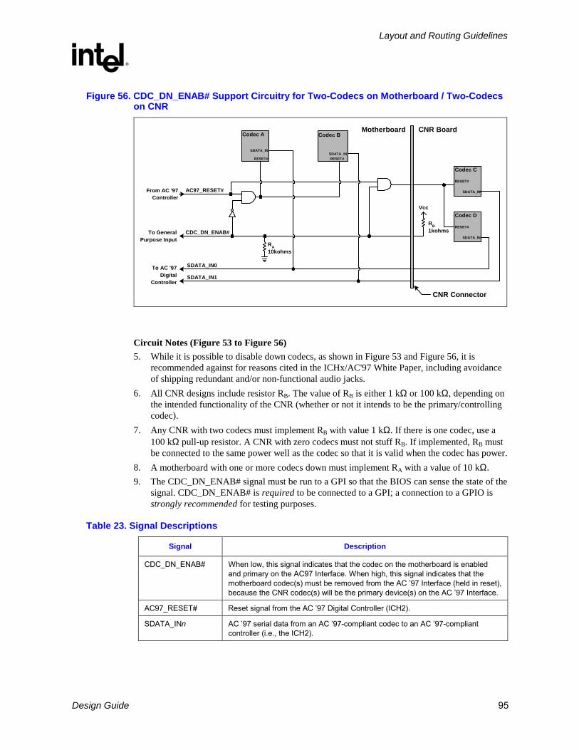
Layout and Routing Guidelines
R
Design Guide 95
Figure 56. CDC_DN_ENAB# Support Circuitry for Two-Codecs on Motherboard / Two-Codecs on CNR
Codec A
RESET#
SDATA_IN
Codec C
RESET#
SDATA_INAC97_RESET#
Vcc
CDC_DN_ENAB#
CNR BoardMotherboard
RA10kohms
RB1kohmsTo General
Purpose Input
From AC '97Controller
CNR Connector
To AC '97Digital
Controller
SDATA_IN0
SDATA_IN1
Codec D
RESET#
SDATA_IN
Codec B
RESET#SDATA_IN
Circuit Notes (Figure 53 to Figure 56) 5. While it is possible to disable down codecs, as shown in Figure 53 and Figure 56, it is
recommended against for reasons cited in the ICHx/AC'97 White Paper, including avoidance of shipping redundant and/or non-functional audio jacks.
6. All CNR designs include resistor RB. The value of RB is either 1 kΩ or 100 kΩ, depending on the intended functionality of the CNR (whether or not it intends to be the primary/controlling codec).
7. Any CNR with two codecs must implement RB with value 1 kΩ. If there is one codec, use a 100 kΩ pull-up resistor. A CNR with zero codecs must not stuff RB. If implemented, RB must be connected to the same power well as the codec so that it is valid when the codec has power.
8. A motherboard with one or more codecs down must implement RA with a value of 10 kΩ. 9. The CDC_DN_ENAB# signal must be run to a GPI so that the BIOS can sense the state of the
signal. CDC_DN_ENAB# is required to be connected to a GPI; a connection to a GPIO is strongly recommended for testing purposes.
Table 23. Signal Descriptions
Signal Description
CDC_DN_ENAB# When low, this signal indicates that the codec on the motherboard is enabled and primary on the AC97 Interface. When high, this signal indicates that the motherboard codec(s) must be removed from the AC 97 Interface (held in reset), because the CNR codec(s) will be the primary device(s) on the AC 97 Interface.
AC97_RESET# Reset signal from the AC 97 Digital Controller (ICH2).
SDATA_INn AC 97 serial data from an AC 97-compliant codec to an AC 97-compliant controller (i.e., the ICH2).

Layout and Routing Guidelines
R
96 Design Guide
6.12.1.1 Valid Codec Configurations
Table 24. Codec Configurations
Valid Codec Configurations Invalid Codec Configurations
AC(Primary) MC(Primary) + X(any other type of codec)
MC(Primary) AMC(Primary) + AMC(Secondary)
AMC(Primary) AMC(Primary) + MC(Secondary)
AC(Primary) + MC(Secondary)
AC(Primary) + AC(Secondary)
AC(Primary) + AMC(Secondary)
6.12.2 SPKR Pin Considerations
The effective impedance of the speaker and codec circuitry on the SPKR signal line must be greater than 50 kΩ. Failure to due so will cause the TCO Timer Reboot function to be erroneously disabled. SPKR is used as both the output signal to the system speaker and as a functional strap. The strap function enables or disables the “TCO Timer Reboot function” based on the state of the SPKR pin on the rising edge of POWEROK. When enabled, the ICH2 sends an SMI# to the processor upon a TCO timer timeout. The status of this strap is readable via the NO_REBOOT bit (bit 1, D31: F0, Offset D4h). The SPKR signal has a weak integrated pull-up resistor (the resistor is only enabled during boot/reset). Therefore, it is default state when the pin is a “no connect” is a logical one or enabled. To disable the feature, a jumper can be populated to pull the signal line low (see figure). The value of the pull-down must be such that the voltage divider caused by the pull-down and integrated pull-up resistors will be read as logic low. When the jumper is not populated, a low can still be read on the signal line if the effective impedance due to the speaker and codec circuit is equal to or lower than the integrated pull-up resistor. It is therefore strongly recommended that the effective impedance be greater than 50 kΩ and the pull-down resistor be less than 7.3 kΩ.
6.13 CNR The Communication and Networking Riser (CNR) Specification defines a hardware-scalable Original Equipment Manufacturer (OEM) motherboard riser and interface. This interface supports multi-channel audio, a V.90 analog modem, phone-line based networking, and 10/100 Ethernet based networking. The CNR specification defines the interface that should be configured before system shipment. Standard I/O expansion slots, such as those supported by the PCI bus architecture, are intended to continue serving as the upgrade medium. The CNR mechanically shares a PCI slot. Unlike in the case of the AMR, the system designer will not sacrifice a PCI slot after deciding not to include a CNR in a particular build.
Figure 57 indicates the interface for the CNR connector. Refer to the appropriate section of this document for the appropriate design and layout guidelines. The Platform LAN Connection (PLC) can either be an 82562EH or 82562ET component. Refer to the CNR specification for additional information.

Layout and Routing Guidelines
R
Design Guide 97
Figure 57. CNR Interface
Communication andnetworking riser
(up to 2 AC '97 codecsand 1 PLC device)
AC '97 I/F
LAN I/F
USB
SMBus
Power
Reserved
Core logiccontroller
IO_subsys_CNR_IF
CNR connector
6.14 USB The general guidelines for the USB interface are as follows:
• Unused USB ports should be terminated with 15 kΩ pull-down resistors on both P+/P- data lines.
• 15 Ω series resistors should be placed as close as possible to the ICH2 (<1 inch). These series resistors are required for source termination of the reflected signal.
• An optional 0 to 47 pF capacitor may be placed as close to the USB connector as possible on the USB data lines (P0+/-, P1+/-, P2+/-, P3+/-). This cap can be used for signal quality (rise/fall time) and to help minimize EMI radiation.
• 15 kΩ ± 5% pull-down resistors should be placed on the USB side of the series resistors on the USB data lines (P0± … P3±), and they are required for signal termination by the USB specification. The stub should be as short as possible.
• The trace impedance for the P0±…P3± signals should be 45 Ω (to ground) for each USB signal P+ or P-. When the stack-up recommended in Figure 34 is used, the USB requires 9-mil traces. The impedance is 90 Ω between the differential signal pairs P+ and P-, to match the 90 Ω USB twisted-pair cable impedance. Note that the twisted-pair’s characteristic impedance of 90 Ω is the series impedance of both wires, resulting in an individual wire presenting a 45 Ω impedance. The trace impedance can be controlled by carefully selecting the trace width, trace distance from power or ground planes, and physical proximity of nearby traces.
• USB data lines must be routed as critical signals. The P+/P- signal pair must be routed together, parallel to each other on the same layer, and not parallel with other non-USB signal traces to minimize crosstalk. Doubling the space from the P+/P- signal pair to adjacent signal traces will help to prevent crosstalk. Do not worry about crosstalk between the two P+/P- signal traces. The P+/P- signal traces must also be the same length. This will minimize the effect of common mode current on EMI. Lastly, do not route over plane splits.

Layout and Routing Guidelines
R
98 Design Guide
Figure 58 illustrates the recommended USB schematic.
Figure 58. USB Data Signals
15 kΩ
15 kΩ
15 Ω
15 Ω
ICH2
P+
P-
< 1"
< 1"
45 Ω
45 Ω
Driver
Driver
Transmission line
Motherboard trace
Motherboard trace
usb_data_line_schem
USB
con
nect
or
90 Ω
USB twisted-pair cable
Optional47 pf
Optional47 pf
The recommended USB trace characteristics are:
• Impedance ‘Z0’ = 45.4 Ω
• Line Delay = 160.2 ps
• Capacitance = 3.5 pF
• Inductance = 7.3 nH
• Res @ 20° C = 53.9 mΩ
6.14.1 Disabling the Native USB Interface of Intel® ICH2
The ICH2 native USB interface can be disabled. This can be done when an external PCI-based USB controller is being implemented in the platform. To disable the native USB Interface, ensure the differential pairs are pulled down thru 15 kΩ resistors, ensure the OC[3:0]# signals are deasserted by pulling them up weakly to VCC3SBY, and that both function 2 & 4 are disabled via the D31:F0;FUNC_DIS register. Ensure that the 48 MHz USB clock is connected to the ICH2 and is kept running. This clock must be maintained even though the internal USB functions are disabled.
6.15 ISA Implementations that require ISA support can benefit from the enhancements of the ICH2, while “ISA-less” designs are not burdened with the complexity and cost of the ISA subsystem. For information regarding the implementation of an ISA design, contact external suppliers.

Layout and Routing Guidelines
R
Design Guide 99
6.16 I/O APIC Design Recommendation UP systems not using the IOAPIC should comply with the following recommendations:
• On the ICH2: Tie PICCLK directly to ground. Tie PICD0, PICD1 to ground through a 10 kΩ resistor.
• On the processor: PICCLK must be connected from the clock generator to the PICCLK pin on the
processor. Tie PICD0 to 2.5 V through 10 kΩ resistors. Tie PICD1 to 2.5 V through 10 kΩ resistors.
6.17 SMBus/SMLink Interface The SMBus interface on the ICH2 is the same as that on the ICH. It uses two signals (SMBCLK and SMBDATA) to send and receive data from components residing on the bus. These signals are used exclusively by the SMBus host controller. The SMBus host controller resides inside the ICH2.
The ICH2 incorporates a new SMLink interface supporting AOL*, AOL2*, and slave functionality. It uses two signals, SMLINK[1:0]. SMLINK[0] corresponds to an SMBus clock signal and SMLINK[1] corresponds to an SMBus data signal. These signals are part of the SMB slave interface.
For Alert on LAN (AOL) functionality, the ICH2 transmits heartbeat and event messages over the interface. When the 82562EM LAN connect component is used, the ICH2’s integrated LAN controller claims the SMLink heartbeat and event messages and sends them out over the network. An external, AOL2-enabled LAN controller will connect to the SMLink signals, to receive heartbeat and event messages as well to as access the ICH2 SMBus slave interface. The slave interface function allows an external microcontroller to perform various functions. For example, the slave write interface can reset or wake a system, generate SMI# or interrupts, and send a message. The slave read interface can read the system power state, read the watchdog timer status, and read system status bits.
Both the SMBus host controller and the SMBus slave interface obey the SMBus protocol, so the two interfaces can be externally wire-ORed together to allow an external management ASIC to access targets on the SMBus as well as the ICH2 slave interface. This is performed by connecting SMLink[0] to SMBCLK and SMLink[1] to SMBDATA, as shown in Figure 59. Since the SMBus and SMLINK are pulled up to VCCSUS3_3, system designers must ensure that they implement proper isolation for any devices that may be powered down while VCCSUS3_3 is still active (i.e., thermal sensors).

Layout and Routing Guidelines
R
100 Design Guide
Figure 59. SMBus/SMLink Interface
82801BA
Host Controller andSlave Interface
SMBus SMBCLK
SPD Data
Temperature onThermal Sensor
NetworkInterface
Card on PCI
Microcontroller
82850
MotherboardLAN Controller
Wire OR(Optional)
SMLink0
SMLink1
SMLink
SMBDATA
smbus-link
Note: Intel does not support external access to the ICH2’s integrated LAN controller via the SMLink interface. Also, Intel does not support access to the ICH2’s SMBus slave interface by the ICH2’s SMBus host controller. Table 25 describes the pull-up requirements for different implementations of the SMBus and SMLink signals.
Table 25. Pull-Up Requirements for SMBus and SMLink
SMBus / SMLink Use Implementation
Alert-on-LAN* signals 4.7 kΩ pull-up resistors to 3.3 VSB are required.
GPIOs Pull-up resistors to 3.3 VSB and the signals must be allowed to change states on power-up. (For example, on power-up the Intel® ICH2 will drive heartbeat messages until the BIOS programs these signals as GPIOs.) The value of the pull-up resistors depends on the loading on the GPIO signal.
Not Used 4.7 kΩ pull-up resistors to 3.3 VSB are required.

Layout and Routing Guidelines
R
Design Guide 101
6.18 PCI The ICH2 provides a PCI Bus interface compliant with the PCI Local Bus Specification, Revision 2.2. The implementation is optimized for high-performance data streaming when the ICH2 is acting as either the target or the initiator on the PCI bus. For more information on the PCI Bus interface, refer to the PCI Local Bus Specification, Revision 2.2.
The ICH2 supports six PCI Bus masters (excluding the ICH2), by providing six REQ#/GNT# pairs. In addition, the ICH2 supports two PC/PCI REQ#/GNT# pairs, one of which is multiplexed with a PCI REQ#/GNT# pair.
Figure 60. PCI Bus Layout Example
IO_subsys_PCI_layout
ICH2
6.19 RTC The ICH2 contains a real-time clock (RTC) with 256 bytes of battery-backed SRAM. The internal RTC module provides two key functions: keeping the date and time, and storing system data in its RAM when the system is powered down.
This section presents the recommended RTC circuit hook-up for ICH2.
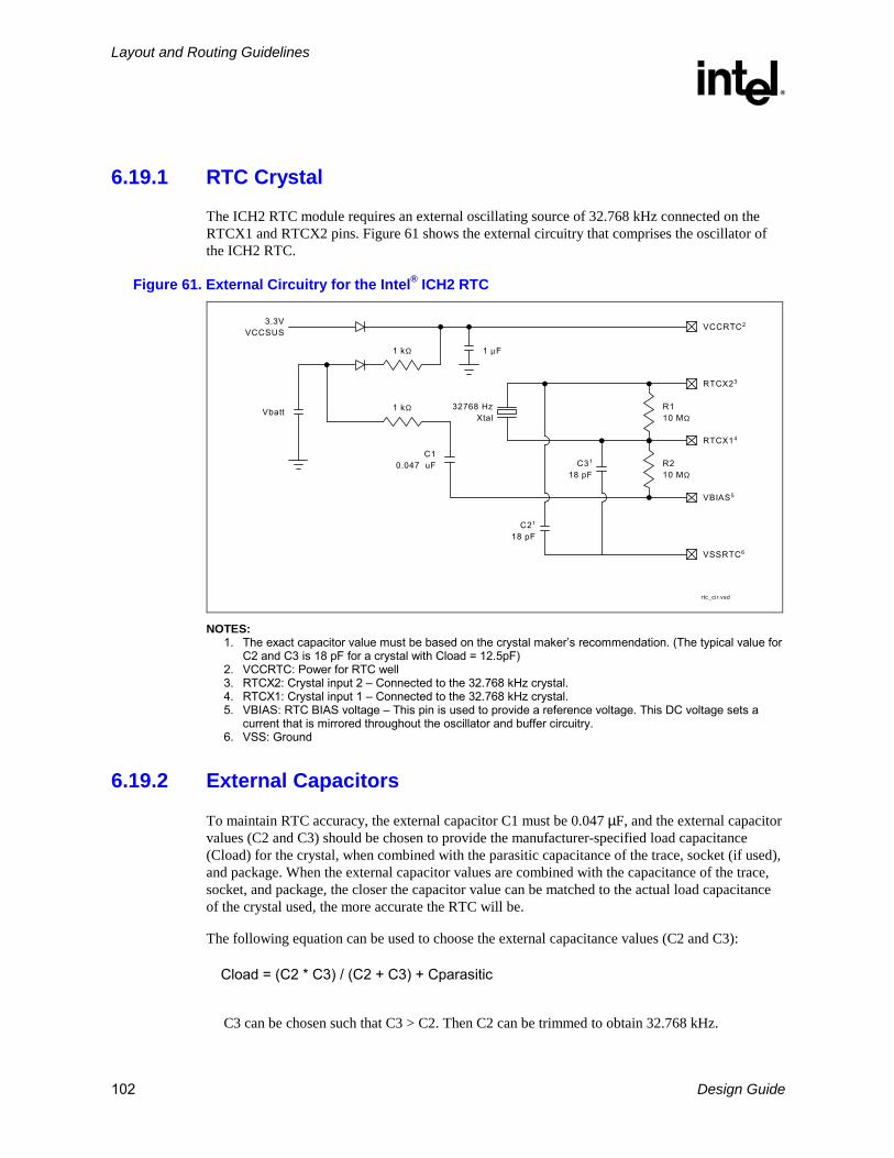
Layout and Routing Guidelines
R
102 Design Guide
6.19.1 RTC Crystal
The ICH2 RTC module requires an external oscillating source of 32.768 kHz connected on the RTCX1 and RTCX2 pins. Figure 61 shows the external circuitry that comprises the oscillator of the ICH2 RTC.
Figure 61. External Circuitry for the Intel® ICH2 RTC
C31
18 pF
3.3VVCCSUS
1 kΩ
Vbatt 1 kΩ
C10.047 uF
32768 HzXtal
R110 MΩ
R210 MΩ
C21
18 pF
1 µF
VCCRTC2
RTCX23
RTCX14
VBIAS5
VSSRTC6
rtc_cir.vsd
NOTES: 1. The exact capacitor value must be based on the crystal makers recommendation. (The typical value for
C2 and C3 is 18 pF for a crystal with Cload = 12.5pF) 2. VCCRTC: Power for RTC well 3. RTCX2: Crystal input 2 Connected to the 32.768 kHz crystal. 4. RTCX1: Crystal input 1 Connected to the 32.768 kHz crystal. 5. VBIAS: RTC BIAS voltage This pin is used to provide a reference voltage. This DC voltage sets a
current that is mirrored throughout the oscillator and buffer circuitry. 6. VSS: Ground
6.19.2 External Capacitors
To maintain RTC accuracy, the external capacitor C1 must be 0.047 µF, and the external capacitor values (C2 and C3) should be chosen to provide the manufacturer-specified load capacitance (Cload) for the crystal, when combined with the parasitic capacitance of the trace, socket (if used), and package. When the external capacitor values are combined with the capacitance of the trace, socket, and package, the closer the capacitor value can be matched to the actual load capacitance of the crystal used, the more accurate the RTC will be.
The following equation can be used to choose the external capacitance values (C2 and C3):
Cload = (C2 * C3) / (C2 + C3) + Cparasitic
C3 can be chosen such that C3 > C2. Then C2 can be trimmed to obtain 32.768 kHz.

Layout and Routing Guidelines
R
Design Guide 103
6.19.3 RTC Layout Considerations • Keep the RTC lead lengths as short as possible. Approximately 0.25 inch is sufficient.
• Minimize the capacitance between Xin and Xout in the routing.
• Put a ground plane under the XTAL components.
• Do not route switching signals under the external components (unless on the other side of the board).
• The oscillator VCC should be clean. Use a filter (e.g., an RC low-pass or a ferrite inductor).
6.19.4 RTC External Battery Connection
The RTC requires an external battery connection to maintain its functionality and its RAM while the ICH2 is not powered by the system.
Example batteries include the Duracell* 2032, 2025 or 2016 (or equivalent), that give many years of operation. Batteries are rated by storage capacity. The battery life can be calculated by dividing the capacity by the average current required. For example, if the battery storage capacity is 170 mAh (assumed usable) and the average current required is 3 µA, the battery life will be at least:
170,000 µAh / 3 µA = 56,666 h = 6.4 years
The voltage of the battery can affect the RTC accuracy. In general, when the battery voltage decays, the RTC accuracy also decreases. High accuracy can be obtained when the RTC voltage is within the range 3.0 V to 3.3 V.
The battery must be connected to the ICH2 via an isolation Schottky diode circuit. The Schottky diode circuit allows the ICH2 RTC well to be powered by the battery when system power is unavailable, but by system power when it is available. So, the diodes are set to be reverse-biased when system power is unavailable. Figure 62 shows an example of the used diode circuitry.
Figure 62. Diode Circuit to Connect RTC External Battery
VCC3_3SBY
VccRTC
1.0 µF
1 kΩ
RTC_ext_batt_diode_circ
-+

Layout and Routing Guidelines
R
104 Design Guide
A standby power supply should be used in a desktop system, to provide continuous power to the RTC when available, which will significantly increase the RTC battery life and thereby the RTC accuracy.
6.19.5 RTC External RTCRST Circuit
Figure 63. RTCRST External Circuit for Intel® ICH2 RTC
VCC3_3SBY
Vcc RTC1.0 µF
1 kΩ
2.2 µF
8.2 kΩRTCRST#
RTCRSTcircuit
Diode /battery circuit
RTC_RTCRESET_ext_circ
The ICH2 RTC requires some additional external circuitry. The RTCRST# signal is used to reset the RTC well. The external capacitor and the external resistor between RTCRST# and the RTC battery (Vbat) were selected to create a RC time delay such that RTCRST# goes high some time after the battery voltage is valid. The RC time delay should be within the range of 10–20 ms. When RTCRST# is asserted, bit 2 (RTC_PWR_STS) in the GEN_PMCON_3 (General PM Configuration 3) register is set to 1 and remains set until cleared by software. As a result, when the system boots, the BIOS knows that the RTC battery has been removed.
This RTCRST# circuit is combined with the diode circuit (see Figure 63) that allows the RTC well to be powered by the battery when system power is unavailable. Figure 63 shows an example of this circuitry when used in conjunction with the external diode circuit.
6.19.6 RTC Routing Guidelines • All RTC OSC signals (RTCX1, RTCX2, VBIAS) should all be routed with trace lengths less
than 1 inch. The shorter, the better.
• Minimize the capacitance between RTCX1 and RTCX2 in the routing. (Optimally, there would be a ground line between them.)
• Put a ground plane under all external RTC circuitry.
• Do not route any switching signals under the external components (unless on the other side of the ground plane).
Layout and Routing Guidelines
R
Design Guide 105
6.19.7 VBIAS DC Voltage and Noise Measurements • All RTC OSC signals (RTCX1, RTCX2, VBIAS) should all be routed with trace lengths less
than 1 inch. The shorter, the better.
• Steady-state VBIAS is a DC voltage of about 0.38 V ± 0.06 V.
• When the battery is inserted, VBIAS will be “kicked” to about 0.7–1.0 V, but it will return to its DC value within a few ms.
• Noise on VBIAS must be kept to a minimum (200 mV or less).
• VBIAS is very sensitive and cannot be directly probed, but it can be probed through a .01 µF capacitor.
• Excessive noise on VBIAS can cause the ICH2 internal oscillator to misbehave or even stop completely.
• To minimize VBIAS noise, it is necessary to implement the routing guidelines described previously as well as the required external RTC circuitry, as described in the Intel® 82801BA I/O Controller Hub 2 (ICH2) and Intel® 82801 BAM I/O Controller Hub 2 Mobile (ICH2-M) Datasheet.
6.19.8 Power-Well Isolation Control
All RTC-well inputs (RSMRST#, RTCRST#, INTRUDER#) must be either pulled up to VCCRTC or pulled down to ground while in G3 state. RTCRST# when configured as shown in Figure 63 meets this requirement. RSMRST# should have a weak external pull-down to ground and INTRUDER# should have a weak external pull-up to VCCRTC. This will prevent these nodes from floating in G3, and correspondingly will prevent ICCRTC leakage that can cause excessive coin-cell drain. The PWROK input signal should also be configured with an external weak pull-down.
The circuit shown in Figure 64, below, should be implemented to control well isolation between the 3.3V resume and RTC power-wells. Failure to implement this circuit may result in excessive droop on the VCCRTC node during Sx-to-G3 power state transitions (removal of AC power).

Layout and Routing Guidelines
R
106 Design Guide
Figure 64. RTC Power-Well Isolation Control
RSMRST#ICH2
from Glue Chipor other source
RSMRST#
2.2k
10kBAV99iP/N 305901-001
BAV99iP/N 305901-001
empty
MMBT3906iP/N 101421-602
empty
6.20 LAN Layout Guidelines The ICH2 provides several options for integrated LAN capability. The platform supports several components, depending on the target market. These guidelines use the 82562ET to refer to both the 82562ET and 82562EM. The 82562EM is specified in those cases where there is a difference.
LAN Connect Component Connection Features
Intel® 82562EM Advanced 10/100 Ethernet AOL* & Ethernet 10/100 connection
Intel® 82562ET 10/100 Ethernet Ethernet 10/100 connection
Intel® 82562EH 1 Mb HomePNA* LAN 1 Mb HomePNA connection
Intel developed a dual footprint for the 82562ET and 82562EH, to minimize the required number of board builds. A single layout with the specified dual footprint allows the OEM to install the appropriate LAN connect component to satisfy market demand. Design guidelines are provided for each required interface and connection. Refer to Figure 65 and Table 26 for the corresponding section of the design guide. Dual footprint guidelines are in Section 6.20.5.
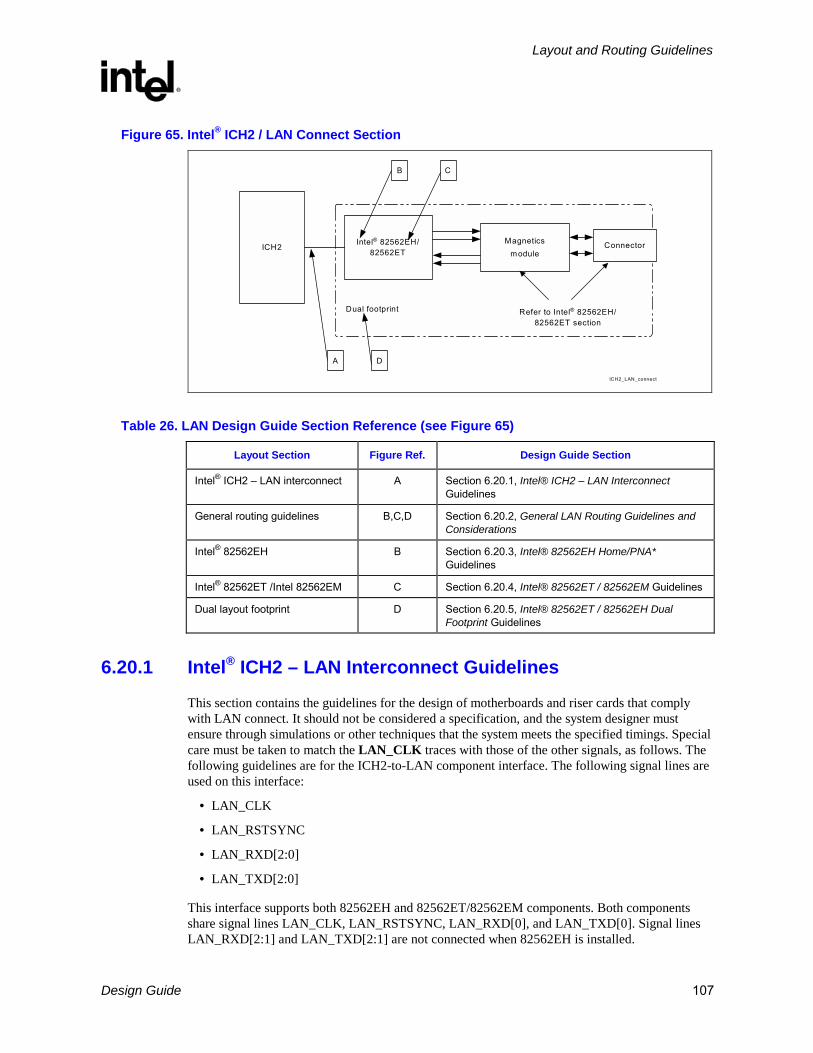
Layout and Routing Guidelines
R
Design Guide 107
Figure 65. Intel® ICH2 / LAN Connect Section
ICH2_LAN_connect
Dual footprint
Intel® 82562EH/82562ET
ICH2Magnetics
moduleConnector
A
B
D
C
Refer to Intel® 82562EH/82562ET section
Table 26. LAN Design Guide Section Reference (see Figure 65)
Layout Section Figure Ref. Design Guide Section
Intel® ICH2 LAN interconnect A Section 6.20.1, Intel® ICH2 – LAN Interconnect Guidelines
General routing guidelines B,C,D Section 6.20.2, General LAN Routing Guidelines and Considerations
Intel® 82562EH B Section 6.20.3, Intel® 82562EH Home/PNA* Guidelines
Intel® 82562ET /Intel 82562EM C Section 6.20.4, Intel® 82562ET / 82562EM Guidelines
Dual layout footprint D Section 6.20.5, Intel® 82562ET / 82562EH Dual Footprint Guidelines
6.20.1 Intel® ICH2 – LAN Interconnect Guidelines
This section contains the guidelines for the design of motherboards and riser cards that comply with LAN connect. It should not be considered a specification, and the system designer must ensure through simulations or other techniques that the system meets the specified timings. Special care must be taken to match the LAN_CLK traces with those of the other signals, as follows. The following guidelines are for the ICH2-to-LAN component interface. The following signal lines are used on this interface:
• LAN_CLK
• LAN_RSTSYNC
• LAN_RXD[2:0]
• LAN_TXD[2:0]
This interface supports both 82562EH and 82562ET/82562EM components. Both components share signal lines LAN_CLK, LAN_RSTSYNC, LAN_RXD[0], and LAN_TXD[0]. Signal lines LAN_RXD[2:1] and LAN_TXD[2:1] are not connected when 82562EH is installed.
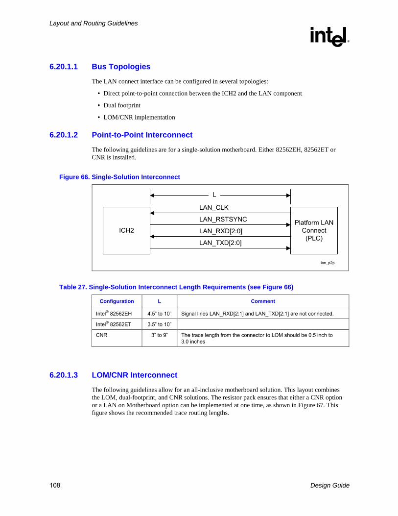
Layout and Routing Guidelines
R
108 Design Guide
6.20.1.1 Bus Topologies
The LAN connect interface can be configured in several topologies:
• Direct point-to-point connection between the ICH2 and the LAN component
• Dual footprint
• LOM/CNR implementation
6.20.1.2 Point-to-Point Interconnect
The following guidelines are for a single-solution motherboard. Either 82562EH, 82562ET or CNR is installed.
Figure 66. Single-Solution Interconnect
lan_p2p
ICH2Platform LAN
Connect(PLC)
LAN_TXD[2:0]
LAN_RXD[2:0]
LAN_RSTSYNC
LAN_CLK
L
Table 27. Single-Solution Interconnect Length Requirements (see Figure 66)
Configuration L Comment
Intel® 82562EH 4.5 to 10 Signal lines LAN_RXD[2:1] and LAN_TXD[2:1] are not connected.
Intel® 82562ET 3.5 to 10
CNR 3 to 9 The trace length from the connector to LOM should be 0.5 inch to 3.0 inches
6.20.1.3 LOM/CNR Interconnect
The following guidelines allow for an all-inclusive motherboard solution. This layout combines the LOM, dual-footprint, and CNR solutions. The resistor pack ensures that either a CNR option or a LAN on Motherboard option can be implemented at one time, as shown in Figure 67. This figure shows the recommended trace routing lengths.
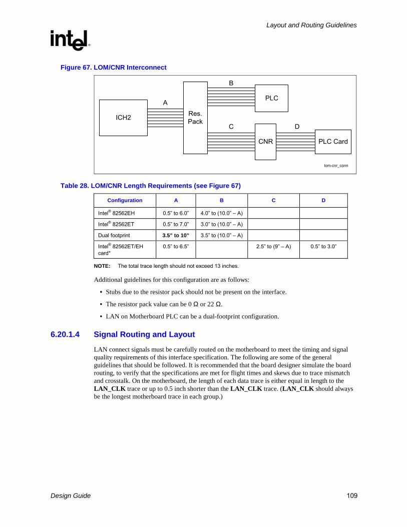
Layout and Routing Guidelines
R
Design Guide 109
Figure 67. LOM/CNR Interconnect
lom-cnr_conn
ICH2 Res.Pack
CNR PLC Card
B
A PLC
C D
Table 28. LOM/CNR Length Requirements (see Figure 67)
Configuration A B C D
Intel® 82562EH 0.5 to 6.0 4.0 to (10.0 A)
Intel® 82562ET 0.5 to 7.0 3.0 to (10.0 A)
Dual footprint 3.5” to 10” 3.5 to (10.0 A)
Intel® 82562ET/EH card*
0.5 to 6.5 2.5 to (9 A) 0.5 to 3.0
NOTE: The total trace length should not exceed 13 inches.
Additional guidelines for this configuration are as follows:
• Stubs due to the resistor pack should not be present on the interface.
• The resistor pack value can be 0 Ω or 22 Ω.
• LAN on Motherboard PLC can be a dual-footprint configuration.
6.20.1.4 Signal Routing and Layout
LAN connect signals must be carefully routed on the motherboard to meet the timing and signal quality requirements of this interface specification. The following are some of the general guidelines that should be followed. It is recommended that the board designer simulate the board routing, to verify that the specifications are met for flight times and skews due to trace mismatch and crosstalk. On the motherboard, the length of each data trace is either equal in length to the LAN_CLK trace or up to 0.5 inch shorter than the LAN_CLK trace. (LAN_CLK should always be the longest motherboard trace in each group.)

Layout and Routing Guidelines
R
110 Design Guide
Figure 68. LAN_CLK Routing Example
LAN_CLK
LAN_RXD0
6.20.1.5 Crosstalk Consideration
Noise due to crosstalk must be carefully minimized. Crosstalk is the main cause of timing skews and is the largest part of the tRMATCH skew parameter.
6.20.1.6 Impedances
Motherboard impedances should be controlled to minimize the impact of any mismatch between the motherboard and the add-in card. An impedance of 60 Ω ± 15% is strongly recommended. Otherwise, signal integrity requirements may be violated.
6.20.1.7 Line Termination
Line termination mechanisms are not specified for the LAN connect interface. Slew-rate-controlled output buffers achieve acceptable signal integrity by controlling signal reflection, over/undershoot, and ringback. A 33 Ω series resistor can be installed at the driver side of the interface, if the developer has concerns about over/undershoot. Note that the receiver must allow for any drive strength and board impedance characteristic within the specified ranges.

Layout and Routing Guidelines
R
Design Guide 111
6.20.2 General LAN Routing Guidelines and Considerations
6.20.2.1 General Trace Routing Considerations
Trace routing considerations are important to minimize the effects of crosstalk and propagation delays on sections of the board where high-speed signals exist. Signal traces should be kept as short as possible to decrease interference from other signals, including those propagated through power and ground planes.
Observe the following suggestions to help optimize board performance:
• The maximum mismatch between the clock trace length and the length of any data trace is 0.5 inch.
• Maintain constant symmetry and spacing between the traces within a differential pair. • Keep the signal trace lengths of a differential pair equal to each other. • Keep the total length of each differential pair under 4 inches. (Many customer designs with
differential traces longer than 5 inches have had one or more of the following issues: IEEE phy conformance failures, excessive EMI, and/or degraded receive BER.)
• Do not route the transmit differential traces closer than 100 mils from the receive differential traces.
• Do not route any other signal traces both parallel to the differential traces and closer than 100 mils to the differential traces (300 mils is recommended).
• Keep to 7 mils the maximum separation between differential pairs. • For high-speed signals, the number of corners and vias should be kept to a minimum. If a 90°
bend is required, it is recommended to use two 45° bends instead. Refer to Figure 69. • Traces should be routed away from board edges by a distance greater than the trace height
above the ground plane. This allows the field around the trace to couple more easily to the ground plane rather than to adjacent wires or boards.
• Do not route traces and vias under crystals or oscillators. This will prevent coupling to or from the clock. And as a general rule, place traces from clocks and drives at a minimum distance from apertures, by a distance exceeding the largest aperture dimension.

Layout and Routing Guidelines
R
112 Design Guide
Figure 69. Trace Routing
45 degreesTrace
45degrees
Trace Geometry and Length
The key factors in controlling trace EMI radiation are the trace length and the ratio of trace width to trace height above the ground plane. To minimize trace inductance, high-speed signals and signal layers close to a ground or power plane should be as short and wide as practical. Ideally, this ratio of trace width to height above the ground plane is between 1:1 and 3:1. To maintain trace impedance, the width of the trace should be modified when changing from one board layer to another, if the two layers are not equidistant from the power or ground plane. Differential trace impedances should be controlled to ~100 Ω. It is necessary to compensate for trace-to-trace edge coupling. This can lower the differential impedance by 10 Ω when the traces within a pair are closer than 0.030 inch (edge-to-edge).
Traces between decoupling and I/O filter capacitors should be as short and wide as practical. Long-and-thin traces are more inductive and would reduce the intended effect of the decoupling capacitors. For similar reasons, traces to I/O signals and signal terminations should be as short as possible. Vias to the decoupling capacitors should have diameters sufficiently large to decrease series inductance. Additionally, the PLC should not be closer than one inch to the connector/magnetics/edge of the board.
Signal Isolation
Comply with the following rules for signal isolation:
• Separate and group signals by function on separate layers if possible. Maintain a gap of 100 mils between all differential pairs (Phoneline and Ethernet) and other nets, but group associated differential pairs together. Note: Over the length of the trace run, each differential pair should be at least 0.3 inch away
from any parallel signal trace.

Layout and Routing Guidelines
R
Design Guide 113
• Physically group together all components associated with one clock trace, to reduce trace length and radiation.
• Isolate I/O signals from high-speed signals to minimize crosstalk, which can increase EMI emission and susceptibility to EMI from other signals.
• Avoid routing high-speed LAN or Phoneline traces near other high-frequency signals associated with a video controller, cache controller, processor or other similar device.
6.20.2.2 Power and Ground Connections
Comply with the following rules and guidelines for power and ground connections:
• All VCC pins should be connected to the same power supply.
• All VSS pins should be connected to the same ground plane.
• Use one decoupling capacitor per power pin for optimized performance.
• Place decoupling as close as possible to power pins.
General Power and Ground Plane Considerations
To properly implement the common-mode choke functionality of the magnetics module, the chassis or output ground (secondary side of transformer) should be physically separated from the digital or input ground (primary side) by at least 100 mils.
Figure 70. Ground Plane Separation
GND_Plane_Separ
Separate Chassis Ground Plane
0.01" minimum separation
Magnetics Module
Separate Chassis Ground Plane Ground plane
Good grounding requires minimizing inductance levels in the interconnections. Keeping ground returns short, signal loop areas small, and power inputs bypassed to signal return will significantly reduce EMI radiation.
Comply with the following rules to help reduce circuit inductance in both backplanes and motherboards:

Layout and Routing Guidelines
R
114 Design Guide
• Route traces over a continuous plane with no interruptions (i.e., do not route over a split plane). If there are vacant areas on a ground or power plane, avoid routing signals over the vacant area. This will increase inductance and EMI radiation levels.
• To reduce coupling, separate noisy digital grounds from analog grounds.
• Noisy digital grounds may affect sensitive DC subsystems.
• All ground vias should be connected to every ground plane, and every power via should be connected to all power planes at equal potential. This helps reduce circuit inductance.
• Physically locate grounds between a signal path and its return. This minimizes the loop area.
• Avoid fast rise/fall times as much as possible. Signals with fast rise and fall times contain many high-frequency harmonics that can radiate EMI.
• The ground plane beneath the filter/transformer module should be split. The RJ45 and/or RJ11 connector side of the transformer module should have chassis ground beneath it. Splitting the ground planes beneath the transformer minimizes noise coupling between the primary and secondary sides of the transformer and between adjacent coils in the transformer. There should not be a power plane under the magnetics module.
• Create a spark gap between pins 2 through 5 of the Phoneline connector(s) and shield ground of 1.6mm (59.0 mil). This is a critical requirement needed to past FCC part 68 testing for Phoneline connection. Note: For worldwide certification a trench of 2.5 mm is required. In North America, the
spacing requirement is 1.6 mm. However, home networking can be used in other parts of the world, including Europe, where some Nordic countries require the 2.5 mm spacing.
6.20.2.3 A 4-Layer Board Design
Top-Layer Routing Sensitive analog signals are routed completely on the top layer without the use of vias. This allows tight control of signal integrity and removes any impedance inconsistencies due to layer changes.
Ground Plane A layout split (100 mils) of the ground plane under the magnetics module between the primary and secondary side of the module is recommended. It is also recommended to minimize the digital noise injected into the 82562 common ground plane. Suggestions include optimizing decoupling on neighboring noisy digital components, isolating the 82562 digital ground using a ground cutout, etc.
Power Plane Physically separate digital and analog power planes must be provided to prevent digital switching noise from being coupled into the analog power supply planes VDD_A. Analog power may be a metal fill “island,” separated from digital power, and better filtered than digital power.
Bottom-Layer Routing Digital high-speed signals, which include all LAN interconnect interface signals, are routed on the bottom layer.

Layout and Routing Guidelines
R
Design Guide 115
6.20.2.4 Common Physical Layout Issues
Common physical layer design and layout mistakes in LAN on Motherboard designs are as follows: 10. Unequal length of the two traces within a differential pair. Inequalities create common-mode
noise and distort transmit or receive waveforms. 11. Lack of symmetry between the two traces within a differential pair. (For each component
and/or via that one trace encounters, the other trace must encounter the same component or a via at the same distance from the PLC.) Asymmetry can create common-mode noise, and distort the waveforms.
12. Excessive distance between the PLC and the magnetics or between the magnetics and the RJ-45/11 connector. Beyond a total distance of about 4 inches, it can become extremely difficult to design a specification-compliant LAN product. Long traces on FR4 (fiberglass epoxy substrate) will attenuate the analog signals. Also any impedance mismatch in the traces will be aggravated if they are longer (see #9 below). The magnetics should be as close to the connector as possible (≤1 inch).
13. Routing any other trace parallel to and close to one of the differential traces. Crosstalk on the receive channel will induce degraded long-cable BER. When crosstalk gets onto the transmit channel, it can cause excessive emissions (below the FCC standard) and can cause poor transmit BER on long cables. Other signals should be kept at least 0.3 inch from the differential traces.
14. Routing the transmit differential traces next to the receive differential traces. The transmit trace closest to one of the receive traces will put more crosstalk onto the closest receive trace; this can greatly degrade the receiver's BER over long cables. After exiting the PLC, the transmit traces should be kept 0.3 inch or more away from the nearest receive trace. In the vicinities where the traces enter or exit the magnetics, the RJ-45/11 and the PLC are the only possible exceptions.
15. Use of an inferior magnetics module. The magnetics modules used by Intel have been fully tested for IEEE PLC conformance, long-cable BER problems, and emissions and immunity. (Inferior magnetics modules often have less common-mode rejection and/or no auto-transformer in the transmit channel.)
16. Another common mistake is using an 82555 or 82558 physical layer schematic in a PLC design. The transmit terminations and decoupling are different, and there also are differences in the receive circuit. Use the appropriate reference schematic or application notes.
17. Not using (or incorrectly using) the termination circuits for the unused pins at the RJ-45/11 and for the wire-side center-taps of the magnetics modules. These unused RJ pins and wire-side center-taps must be correctly referenced to chassis ground via the proper value resistor and capacitor or termination plane. If these are not terminated properly, there can be emission (FCC) problems, IEEE conformance issues, and long-cable noise (BER) problems. The application notes contain schematics that illustrate the proper termination for these unused RJ pins and the magnetics center-taps.

Layout and Routing Guidelines
R
116 Design Guide
18. Incorrect differential trace impedances. It is important to have ~100 Ω impedance between the two traces within a differential pair. This becomes even more important as the differential traces become longer. It is very common to see customer designs that have differential trace impedances between 75 Ω and 85 Ω, even when the designers think they have designed for 100 Ω. (To calculate the differential impedance, many impedance calculators only multiply the single-ended impedance by two. This does not take into account edge-to-edge capacitive coupling between the two traces. When the two traces within a differential pair are kept close (see Note) to each other, the edge coupling can lower the effective differential impedance by 5 Ω to 20 Ω. A 10 Ω to 15 Ω drop in impedance is common.) Short traces will have fewer problems if the differential impedance is a little off.
19. Another common problem is to use a too-large capacitor between the transmit traces and/or too much capacitance from the magnetic's transmit center-tap (on the 82562ET side of the magnetics) to ground. Using capacitors with capacitances exceeding a few pF in either of these locations can slow the 100 Mbps rise and fall times so much that they fail the IEEE rise time and fall time specifications. This will cause the return loss to fail at higher frequencies and will degrade the transmit BER performance. Caution should be exercised if a cap is put in either of these locations. If a cap is used, it should almost certainly be less than 22 pF. (Reasonably good success has been achieved by using 6 pF to 12 pF values in past designs.) Unless there is some overshoot in the 100 Mbps mode, these caps are not necessary.
Note: It is important to keep the two traces within a differential pair close to each other. Keeping them close helps to make them more immune to crosstalk and other sources of common-mode noise. This also means lower emissions (i.e., FCC compliance) from the transmit traces and better receive BER for the receive traces. Close should be considered to be less than 0.030 inch between the two traces within a differential pair (0.007 inch trace-to-trace spacing is recommended).
6.20.3 Intel® 82562EH Home/PNA* Guidelines
For correct LAN performance, designers must follow the general guidelines outlined in Section 6.20.2. Additional guidelines for implementing an 82562EH Home/PNA* LAN connect component are listed in the following sections. Refer to Section 1.2 for a list of related documents.
6.20.3.1 Power and Ground Connections
Obey the following rule for power and ground connections:
• For best performance, place decoupling capacitors on the back side of the PCB, directly under the 82562EH, with equal distance from both pins of the capacitor to power/ground.
The analog power supply pins for the 82562EH (VCCA, VSSA) should be isolated from the digital VCC and VSS through the use of ferrite beads. In addition, adequate filtering and decoupling capacitors should be provided between VCC and VSS as well as the VCCA and VSSA power supplies.
6.20.3.2 Guidelines for Intel® 82562EH Component Placement
Component placement can affect the signal quality, emissions, and temperature of a board design. This section discusses guidelines for component placement.
Careful component placement can:

Layout and Routing Guidelines
R
Design Guide 117
• Decrease potential problems directly related to electromagnetic interference (EMI), which could result in failure to meet FCC specifications.
• Simplify the task of routing traces. To some extent, component orientation will affect the complexity of trace routing. The overall objective is to minimize turns and crossovers between traces.
It is important to minimize the space needed for the HomePNA LAN interface, because all other interfaces will compete for physical space on a motherboard near the connector edge. As with most subsystems, the HomePNA LAN circuits must be as close as possible to the connector. Thus, it is imperative that all designs be optimized to fit in a very small space.
6.20.3.3 Crystals and Oscillators
To minimize the effects of EMI, clock sources should not be placed near I/O ports or board edges. Radiation from these devices may be coupled onto the I/O ports or out of the system chassis. Crystals should also be kept away from the HomePNA magnetics module to prevent communication interference. If they exist, the crystal’s retaining straps should be grounded to prevent the possibility of radiation from the crystal case, and the crystal should lie flat against the PC board to provide better coupling of the electromagnetic fields to the board.
For noise-free and stable operation, place the crystal and associated discrete components as close as possible to the 82562EH. Minimize the length and do not route any noisy signals in this area.
6.20.3.4 Phoneline HPNA Termination
The transmit/receive differential signal pair is terminated with a pair of 51.1 Ω (1%) resistors. This parallel termination should be placed close to the Intel 82562EH. The center, common point between the 51.1 Ω resistors is connected to a voltage-divider network. The termination is shown in Figure 71.

Layout and Routing Guidelines
R
118 Design Guide
Figure 71. Intel® 82562EH Termination
123456
Tab
Tab
123456
Tab
Tab
8Phone / modem
Shield ground
Line 8
7
7
IO_subsys_82562EH_term
1500 pF 1500 pF
6.8 µH 6.8 µH
6.8 µH 6.8 µH
0
T10
9
1
23
B6008
rx_tx_p
rx_tx_n
0.022 µF
51.1 Ω
51.1 Ω
806 Ω
806 Ω
A+3.3 V
Tip
Ring
The filter and magnetics component T1 integrates the required filter network, high-voltage impulse protection, and transformer to support the HomePNA LAN interface.
One RJ-11 jack (labeled “LINE” in the previous figure) allows the node to be connected to the Phoneline, and the second jack (labeled “PHONE” in the previous figure) allows other down-line devices to be connected at the same time. This second connector is not required by the HomePNA. However, typical PCI adapters and PC motherboard implementations are likely to include it for user convenience.
A low-pass filter, setup in-line with the second RJ-11 jack, also is recommended by the HomePNA to minimize interference between the HomeRun connection and a POTs voice or modem connection on the second jack. This restricts of the type of devices connected to the second jack as the pass-band of this filter is set approximately at 1.1 MHz. Refer to the HomePNA website (www.homepna.org) for up-to-date information and recommendations regarding the use of this low-pass filter to meet HomePNA certifications.
6.20.3.5 Critical Dimensions
There are three dimensions to consider during layout. Distance ‘B’ from the line RJ11 connector to the magnetics module, distance ‘C’ from the phone RJ11 to the LPF (if implemented), and distance ‘A’ from 82562EH to the magnetics module (see Figure 72).

Layout and Routing Guidelines
R
Design Guide 119
Figure 72. Critical Dimensions for Component Placement
LAN_crit_dim_comp_place
ICH2 Intel®
82562ETMagnetics
moduleLineRJ11
BA
EEPROM
LPF PhoneRJ11
C
Table 29. Critical Dimensions for Component Placement (see Figure 72)
Distance Priority Guideline
B 1 < 1 inch
A 2 < 1 inch
C 3 < 1 inch
Distance from Magnetics Module to Line RJ11
This distance ‘B’ should be given highest priority and should be less then 1 inch. Regarding trace symmetry, route differential pairs with consistent separation and with exactly the same lengths and physical dimensions.
Asymmetrical and unequally long differential pairs contribute to common-mode noise. This can degrade receive circuit performance and contribute to emissions radiated from the transmit side.
Distance from Intel® 82562EH to Magnetics Module
Due to the high speed of signals present, distance ‘A’ between the 82562EH and the magnetic should also be less than 1 inch, but should be second priority relative to distance from connects to the magnetic module.
Generally speaking, any section of trace intended for use with high-speed signals should be subject to proper termination practices. Proper signal termination can reduce reflections caused by impedance mismatches between the device and trace route. The reflections of a signal may have a high-frequency component that may contribute more EMI than the original signal itself.
Distance from LPF to Phone RJ11
This distance ‘C’ should be less then 1 inch. Regarding trace symmetry, route differential pairs with consistent separation and with exactly the same lengths and physical dimensions.

Layout and Routing Guidelines
R
120 Design Guide
Asymmetrical and unequally long differential pairs contribute to common-mode noise. This can degrade the receive circuit performance and contribute to emissions radiated from the transmit side.
6.20.4 Intel® 82562ET / 82562EM Guidelines
For correct LAN performance, designers must follow the general guidelines outlined in Section 6.20.2. Additional guidelines for implementing an 82562ET or 82562EM LAN connect component are provided in the following sub-sections. For additional information, refer to the Intel® 82562ET Platform LAN Connect (PLC) Datasheet and PCB Design for the Intel® 82562 ET/EM Platform LAN Connect.
6.20.4.1 Guidelines for Intel® 82562ET / 82562EM Component Placement
Component placement can affect the signal quality, emissions, and temperature of a board design. This section provides guidelines for component placement.
Careful component placement can:
• Decrease potential problems directly related to electromagnetic interference (EMI), which could result in failure to meet FCC and IEEE test specifications.
• Simplify the task of routing traces. To some extent, component orientation will affect the complexity of trace routing. The overall objective is to minimize turns and crossovers between traces.
It is important to minimize the space needed for the Ethernet LAN interface, because all other interfaces will compete for physical space on a motherboard near the connector edge. As with most subsystems, the Ethernet LAN circuits must be as close as possible to the connector. Thus, it is imperative that all designs be optimized to fit in a very small space.
6.20.4.2 Crystals and Oscillators
To minimize the effects of EMI, clock sources should not be placed near I/O ports or board edges. Radiation from these devices may be coupled onto the I/O ports or out of the system chassis. Crystals should also be kept away from the Ethernet magnetics module to prevent interference with communication. If they exist, the retaining straps of the crystal should be grounded to prevent possible radiation from the crystal case. Also, the crystal should lie flat against the PC board to provide better coupling of the electromagnetic fields to the board.
For noise-free and stable operation, place the crystal and associated discrete components as close as possible to the 82562ET or 82562EM. Keep the trace length as short as possible and do not route any noisy signals in this area.
6.20.4.3 Intel® 82562ET / 82562EM Termination Resistors
The 100 Ω (1%) resistor used to terminate the differential transmit pairs (TDP/TDN) and the 120 Ω (1%) receive differential pairs (RDP/RDN) should be placed as close as possible to the LAN connect component (82562ET or 82562EM) as possible. This is due to the fact that these resistors terminate the entire impedance seen at the termination source (i.e., 82562ET), including the wire impedance reflected through the transformer.

Layout and Routing Guidelines
R
Design Guide 121
Figure 73. Intel® 82562ET/82562EM Termination
LAN_82562ET-82562EM_term
Intel®
82562ETMagnetics
moduleRJ45
Place termination resistors as closeas possible to Intel® 82562ET.
LAN connectinterface
6.20.4.4 Critical Dimensions
There are two dimensions to consider during layout. Distance ‘B’ from the line RJ45 connector to the magnetics module and distance ‘A’ from the 82562ET or 82562EM to the magnetics module (see Figure 74).
Figure 74. Critical Dimensions for Component Placement
LAN_crit_dim_comp_place_2
ICH2 Intel®
82562EHMagnetics
moduleLineRJ11
BA
EEPROM
LPF PhoneRJ11
C
Table 30. Critical Dimensions for Component Placement (see Figure 74)
Distance Priority Guideline
A 1 < 1 inch
B 2 < 1 inch
Distance from Magnetics Module to RJ45
The distance A in Figure 74 should be given the highest priority in board layout. The separation between the magnetic module and the RJ45 connector should be kept less than 1 inch. The following trace characteristics are important and should be observed:

Layout and Routing Guidelines
R
122 Design Guide
• Differential impedance: The differential impedance should be 100 Ω. The single-ended trace impedance will be approximately 50 Ω. However, the differential impedance can also be affected by the spacing between the traces.
• Trace Symmetry: Differential pairs (e.g., TDP and TDN) should be routed with consistent separation and with exactly the same lengths and physical dimensions (e.g., width).
Caution: Asymmetric and unequal length traces in the differential pairs contribute to common-mode noise. This can degrade the receive circuit’s performance and contribute to emissions radiated from the transmit circuit. If the 82562ET must be placed farther than a couple of inches from the RJ45 connector, distance B can be sacrificed. It should be a priority to keep the total distance between the 82562ET and RJ45 as short as possible.
Note: The measured trace impedance for layout designs targeting 100 Ω often result in lower actual impedance. OEMs should verify actual trace impedance and adjust their layouts accordingly. If the actual impedance is consistently low, a target of 105–110 Ω should compensate for second-order effects.
Distance from Intel® 82562ET to Magnetics Module
Distance B should also be designed to be less than 1 inch between devices. The high-speed nature of the signals propagating through these traces requires that the distance between these components be closely observed. In general, any section of traces intended for use with high-speed signals should be subject to proper termination practices. Proper termination of signals can reduce reflections caused by impedance mismatches between device and traces. The reflections of a signal may have a high-frequency component that contributes more EMI than the original signal itself. For this reason, these traces should be designed to a 100 Ω differential value. These traces should also be symmetric and of equal length within each differential pair.
6.20.4.5 Reducing Circuit Inductance
The following guidelines show how to reduce circuit inductance in both backplanes and motherboards. Traces should be routed over a continuous ground plane with no interruptions. If there are vacant areas on a ground or power plane, the signal conductors should not cross the vacant area. This increases inductance and associated radiated noise levels. Noisy logic grounds should be separated from analog signal grounds to reduce coupling. Noisy logic grounds can sometimes affect sensitive DC subsystems, such as analog-to-digital conversion, operational amplifiers, etc. All ground vias should be connected to every ground plane. Similarly, every power via should be connected to all power planes at equal potential. This helps reduce circuit inductance. Another recommendation is to physically locate grounds so as to minimize the loop area between a signal path and its return path. Rise and fall times should be as slow as possible. Because signals with fast rise and fall times contain many high-frequency harmonics, they can radiate significantly. The most sensitive signal returns closest to the chassis ground should be connected together. This will result in a smaller loop area and reduce the likelihood of crosstalk. The effect of different configurations on the amount of crosstalk can be studied using electronics modeling software.

Layout and Routing Guidelines
R
Design Guide 123
Terminating Unused Connections
In Ethernet designs, it is common practice to terminate to ground both unused connections on the RJ45 connector and the magnetics module. Depending on the overall shielding and grounding design, this may be done to the chassis ground, signal ground or a termination plane. Care must be taken when using various grounding methods to ensure that emission requirements are met. The method most often implemented is called the “Bob Smith” termination. In this method, a floating termination plane is cut out of a power plane layer. This floating plane acts as a plate of a capacitor with an adjacent ground plane. The signals can be routed through 75 Ω resistors to the plane. Stray energy on unused pins is then carried to the plane.
Termination Plane Capacitance
The recommended minimum termination plane capacitance is 1500 pF. This helps reduce the amount of crosstalk on the differential pairs (TDP/TDN and RDP/RDN) from the unused pairs of the RJ45. Pads may be placed for an additional capacitance to chassis ground, which may be required if the termplane capacitance is not large enough to pass EFT (electrical fast transient) testing. If a discrete capacitor is used, it should be rated for at least 1000 VAC, to satisfy the EFT requirements.
Figure 75. Termination Plane
N/C
RJ-45
Magnetics Module
RDP
RDN
TDP
TDN
Termination Plane
Additional capacitance that may needto be added for EFT testing
term_plane
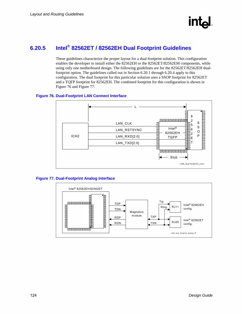
Layout and Routing Guidelines
R
124 Design Guide
6.20.5 Intel® 82562ET / 82562EH Dual Footprint Guidelines
These guidelines characterize the proper layout for a dual-footprint solution. This configuration enables the developer to install either the 82562EH or the 82562ET/82562EM components, while using only one motherboard design. The following guidelines are for the 82562ET/82562EH dual-footprint option. The guidelines called out in Section 6.20.1 through 6.20.4 apply to this configuration. The dual footprint for this particular solution uses a SSOP footprint for 82562ET and a TQFP footprint for 82562EH. The combined footprint for this configuration is shown in Figure 76 and Figure 77.
Figure 76. Dual-Footprint LAN Connect Interface
LAN_dual-footprint_conn
ICH2
LAN_TXD[2:0]
LAN_RXD[2:0]
LAN_RSTSYNC
LAN_CLK
L
82562ET
SSOP
Stub
Intel®
82562EHTQFP
Figure 77. Dual-Footprint Analog Interface
LAN_dual_footprint_analog_IF
Magneticsmodule
TDP
RJ45
Intel® 82562EH/82562ET
TDN
RDP
RDN
RJ11
TXP
TXN
Tip
RingIntel® 82562EHconfig.
Intel® 82562ETconfig.

Layout and Routing Guidelines
R
Design Guide 125
The following are additional guidelines for this configuration:
• L = 0.5 inch to 6.5 inches
• Stub < 0.5 inch
• Either 82562EH or 82562ET/82562EM can be installed, but not both.
• Intel 82562ET pins 28, 29, and 30 overlap with 82562EH pins 17, 18, and 19.
• Overlapping pins are tied to ground.
• No other signal pads should overlap or touch.
• Signal lines LAN_CLK, LAN_RSTSYNC, LAN_RXD[0], LAN_TXD[0], RDP, RDN, RXP/Ring, and RXN/Tip are shared by the 82562EH and 82562ET configurations.
• No stubs should be present when 82562ET is installed.
• Packages used for the dual footprint are TQFP for 82562EH and SSOP for 82562ET.
• A 22 Ω resistor can be placed at the driving side of the signal line to improve signal quality on the LAN connect interface.
• Resistor should be placed as close as possible to the component.
• Use components that can satisfy both the 82562ET and 82562EH configurations (i.e., magnetics module).
• Install components for either the 82562ET or the 82562EH configuration. Only one configuration can be installed at a time.
• Route shared signal lines such that stubs are not present or are kept to a minimum.
• Stubs may occur on shared signal lines (i.e., RDP and RDN). These stubs are due to traces routed to an uninstalled component.
• Use 0 Ω resistors to connect and disconnect circuitry not shared by both configurations. Place resistor pads along the signal line to reduce stub lengths.

Layout and Routing Guidelines
R
126 Design Guide
6.21 LPC/FWH The following provides general guidelines for compatibility and design recommendations for supporting the FWH flash BIOS device. The majority of the changes will be incorporated in the BIOS.
6.21.1 In-Circuit FWH Programming All cycles destined for the FWH will appear on the PCI. The ICH2 hub interface-to-PCI Bridge puts all processor boot cycles out on the PCI (before sending them out on the FWH interface). If the ICH2 is set for subtractive decode, these boot cycles can be accepted by a positive decode agent on PCI. This enables booting from a PCI card that positively decodes these memory cycles. To boot from a PCI card, it is necessary to keep the ICH2 in the subtractive decode mode. If a PCI boot card is inserted and the ICH2 is programmed for positive decode, two devices will positively decode the same cycle. In systems with the 82380AB (ISA bridge), it is also necessary to keep the NOGO signal asserted when booting from a PCI ROM. Note that it is not possible to boot from a ROM behind the 82380AB. Once you have booted from the PCI card, you potentially could program the FWH in circuit and program the ICH2 CMOS.
6.21.2 FWH Vpp Design Guidelines The Vpp pin on the FWH is used for programming the flash cells. The FWH supports a Vpp of 3.3 V or 12 V. If Vpp is 12 V, the flash cells will program about 50% faster than at 3.3 V. However, the FWH only supports 12 Vpp for 80 hours. The 12 Vpp would be useful in a programmer environment that is typically an event that occurs very infrequently (much less than 80 hours). The VPP pin MUST be tied to 3.3 V on the motherboard.
In some instances, it is desirable to program the FWH during assembly with the device soldered down on the board. To decrease programming time it becomes necessary to apply 12 V to the VPP pin. Figure 78 shows a circuit that allows testers to put 12 V on the VPP pin while keeping this voltage separated from the 3.3 V plane to which the rest of the power pins are connected. This circuit also allows the board to operate with 3.3 V on this pin during normal operation.
Figure 78. FWH VPP Isolation Circuitry
1K
FET
12V 3.3V
VPP

Layout and Routing Guidelines
R
Design Guide 127
6.21.3 FWH Decoupling A 0.1 µF capacitor should be placed between the VCC supply pins and the VSS ground pins to decouple high frequency noise, which may affect the programmability of the device. Additionally, a 4.7 µF capacitor should be placed between the VCC supply pins and the VSS ground pin to decouple low frequency noise. The capacitors should be placed no further than 390 mils from the VCC supply pins.
6.22 Processor PLL Filter Recommendation
6.22.1 Processor PLL Filter Recommendation
All Celeron processors have internal PLL clock generators that are analog and require quiet power supplies to minimize jitter.
6.22.2 Topology
The general desired topology is shown in Figure 79. Not shown are parasitic routing and local decoupling capacitors. Excluded from the external circuitry are parasitics associated with each component.
Figure 79. Filter Topology
v004
R L
C
PLL2
PLL1
PLL
VSS = 0V
370-PinSocket
VCCCORE
6.22.3 Filter Specification
The function of the filter is to protect the PLL from external noise through low-pass attenuation. In general, the low-pass description forms an adequate description for the filter.

Layout and Routing Guidelines
R
128 Design Guide
The low-pass specification, with input at VCCCORE and output measured across the capacitor, is as follows:
< 0.2 dB gain in pass band
< 0.5 dB attenuation in pass band (see DC drop in next set of requirements)
> 34 dB attenuation from 1 MHz to 66 MHz
> 28 dB attenuation from 66 MHz to core frequency
The filter specification is graphically shown in Figure 80.
Figure 80. Filter Specification
0dB
-28dB
-34dB
0.2dB
x dB
1 MHz 66 MHz fcorefpeak1HzDC
passband high frequencyband
x = 20.log[(Vcc-60mV)/Vcc]filter1.vsd
NOTES: 1. Diagram not to scale. 2. No specification for frequencies beyond fcore. 3. fpeak, if it exists, should be less than 0.05 MHz.
Other requirements:
• Filter should support DC current > 30 mA.
• Shielded type inductor to minimize magnetic pickup.
• DC voltage drop from VCC to PLL1 should be < 60mV, which in practice implies series R < 2 Ω; also means pass band (from DC to 1Hz) attenuation < 0.5dB for VCC = 1.1V, and < 0.35dB for VCC = 1.5V.
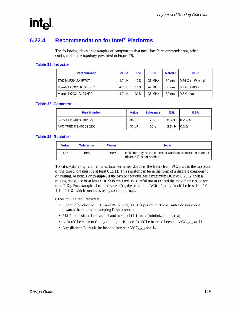
Layout and Routing Guidelines
R
Design Guide 129
6.22.4 Recommendation for Intel® Platforms
The following tables are examples of components that meet Intel’s recommendations, when configured in the topology presented in Figure 79.
Table 31. Inductor
Part Number Value Tol SRF Rated I DCR
TDK MLF2012A4R7KT 4.7 uH 10% 35 MHz 30 mA 0.56 Ω (1 W max)
Murata LQG21N4R7K00T1 4.7 uH 10% 47 MHz 30 mA 0.7 Ω (±50%)
Murata LQG21C4R7N00 4.7 uH 30% 35 MHz 30 mA 0.3 Ω max
Table 32. Capacitor
Part Number Value Tolerance ESL ESR
Kemet T495D336M016AS 33 µF 20% 2.5 nH 0.225 Ω
AVX TPSD336M020S0200 33 µF 20% 2.5 nH 0.2 Ω
Table 33. Resistor
Value Tolerance Power Note
1 Ω 10% 1/16W Resistor may be implemented with trace resistance in which discrete R is not needed
To satisfy damping requirements, total series resistance in the filter (from VCCCORE to the top plate of the capacitor) must be at least 0.35 Ω. This resistor can be in the form of a discrete component, or routing, or both. For example, if the picked inductor has a minimum DCR of 0.25 Ω, then a routing resistance of at least 0.10 Ω is required. Be careful not to exceed the maximum resistance rule (2 Ω). For example, if using discrete R1, the maximum DCR of the L should be less than 2.0 - 1.1 = 0.9 Ω, which precludes using some inductors.
Other routing requirements: • C should be close to PLL1 and PLL2 pins, < 0.1 Ω per route. These routes do not count
towards the minimum damping R requirement. • PLL2 route should be parallel and next to PLL1 route (minimize loop area). • L should be close to C; any routing resistance should be inserted between VCCCORE and L. • Any discrete R should be inserted between VCCCORE and L.

Layout and Routing Guidelines
R
130 Design Guide
Figure 81. Using Discrete R
v005
L
C
<0.1 ohm route
PLL2
PLL1
370-PinSocket
<0.1 ohm route
R
VCCCORE
Discrete Resistor
Figure 82. No Discrete R
v006
L
C
<0.1 ohm route
PLL2
PLL1
370-PinSocket
<0.1 ohm route
VCCCORE
Trace Resistance
6.22.5 Custom Solutions
As long as filter performance as specified in the previous “Filter Specification” figure and other requirements outlined in Section 6.22.1. are satisfied, other solutions are acceptable. Custom solutions should be simulated against a standard reference core model, which is shown in Figure 83.
Figure 83. Core Reference Model
PLL1
PLL2
Processor0.1 ohm
120pF 1K ohm
0.1 ohm
NOTES: 1. 0.1 Ω resistors represent package routing1. 2. 120 pF capacitor represents internal decoupling capacitor. 3. 1 kΩ resistor represents small signal PLL resistance. 4. Be sure to include all component and routing parasitics. 5. Please sweep across component/parasitic tolerances. 6. To observe IR drop, use DC current of 30 mA and minimum VCCCORE level.
1 For other modules (interposer, DMM, etc), adjust routing resistor if desired, but use minimum numbers.

Layout and Routing Guidelines
R
Design Guide 131
6.23 RAMDAC/Display Interface Figure 84 shows the interface of the RAMDAC analog current outputs with the display. Each DAC output is doubly-terminated with a 75 Ω resistance; one 75 Ω resistance from the DAC output to the board ground and the other termination resistance exists within the display. The equivalent DC resistance at the output of each DAC output is 37.5 Ω. The output current of each DAC flows into this equivalent resistive load to produce a video voltage without the need for external buffering. There is also an LC pi-filter that is used to reduce high-frequency glitches and noise, and reduce EMI. To maximize the performance, the filter impedance, cable impedance, and load impedance should be the same. The LC pi-filter consists of two 3.3 pF capacitors and a ferrite bead with a 75 Ω impedance at 100 MHz. The LC pi-filter is designed to filter glitches produced by the RAMDAC while maintaining adequate edge rates to support high-end display resolutions.
Figure 84. Schematic of RAMDAC Video Interface
RAMDAC
VCCDACA1/VCCDACA2 VCCDA RED
GraphicsChip
PixelClock(FromDPLL)
Cf
Lf
LCFilter
1.8V BoardPower Plane
Display PLL PowerConnects to this
Segmented PowerPlane 1.8V Board
Power Plane
1.8V BoardPower Plane
Rt D2
D1
C1 C2
FB
pi Filter1.8V Board
Power Plane
Rt D2
D1
C1 C2
FB
pi Filter1.8V Board
Power Plane
Rt D2
D1
C1 C2
FB
pi Filter
GREEN
Blue
VSSDACA
AnalogPower Plane
1.8V
IREFIWASTE
Ground Plane
Rset 1% ReferenceCurrent Resistor(metal film)
VideoConnector
Graphics Board
Red
Green
Blue
CoaxCableZo=75Ω
75Ω
75Ω
75Ω
Display
Termination Resistor, R 75Ω 1% (metal film)
Diodes D1, D2: Schottky Diodes
LC Filter Capacitors, C1, C2: 3.3 pF
Ferrite Bead, FB: 7 Ω @ 100 MHz(Recommended part: muRataBLM11B750S)
ramdac3.vsd
NOTE: Diodes D1, D2 are clamping diodes and may not be necessary to populate.

Layout and Routing Guidelines
R
132 Design Guide
In addition to the termination resistance and LC pi-filter, there are protection diodes connected to the RAMDAC outputs to help prevent latch-up. The protection diodes must be connected to the same power supply rails as the RAMDAC. An LC filter is recommended to connect the segmented analog 1.8V power plane of the RAMDAC to the 1.8V board power plane. The LC filter is recommended to be designed for a cut-off frequency of 100 kHz.
6.23.1 Reference Resistor (Rset) Calculation
The full-swing video output is designed to be 0.7V according to the VESA video standard. With an equivalent DC resistance of 37.5 Ω (two 75 Ω in parallel - one 75 Ω termination on the board and one 75 Ω termination within the display), the full-scale output current of a RAMDAC channel is 0.7/37.5 Ω = 18.67 mA. Since the RAMDAC is an 8-bit current-steering DAC, this full-scale current is equivalent 255I, where I is a unit of current. Therefore, the unit current or LSB current of the DAC signals equals 73.2 µA. The reference circuitry generates a voltage across this Rset resistor equal to a bandgap voltage divided-by-three (409 mV). The RAMDAC reference current generation circuitry is designed to generate a 32I reference current using the reference voltage and the Rset value. To generate a 32I reference current for the RAMDAC, the reference current setting resistor, Rset, is calculated from the following equation:
Rset = VREF/32I = 0.409V/32*73.2µA = 174 Ω
6.23.2 RAMDAC Board Design Guidelines
The RAMDAC layout is shown in Figure 85, Figure 86, and Figure 87. An RLC network should be used between the board power plane and the board ground plane. The recommended RAMDAC routing for a four layer board is such that the red, green and blue video outputs be routed on the top (bottom) layer over (under) a solid ground plane to maximize noise rejection characteristics of the video outputs. It is essential to avoid toggling signals from being routed next to the video output signals to the VGA connector. A 20 mil spacing between any video route and any other routes is recommended.
Matching of the video routes (red, green, and blue) from the RAMDAC to the VGA connector is also essential. The routing for these signals should be as similar as possible (i.e., same routing layer(s), same number of vias, same routing length, same bends and jogs).
Figure 85 shows recommended RAMDAC component placement and routing. The termination resistance can be placed anywhere along the video route from the RAMDAC output to the VGA connector as long as the impedance of the traces are designed as indicated in Figure 85. The pi- filters are recommended to be placed in close proximity to the VGA connector to maximize EMI filtering effectiveness. The LC filter components for the RAMDAC/PLL power plane, de-coupling capacitors, latch-up protection diodes, and the reference resistor are recommended to be placed in close proximity to the respective pins.
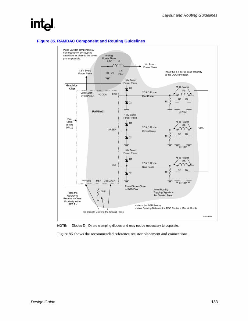
Layout and Routing Guidelines
R
Design Guide 133
Figure 85. RAMDAC Component and Routing Guidelines
RAMDAC
VCCDACA1/VCCDACA2 VCCDA RED
GraphicsChip
PixelClock(FromDPLL)
Cf
Lf
LCFilter
1.8V BoardPower Plane
Place LC filter components &high frequency de-couplingcapacitors as close to the powerpins as possible.
1.8V BoardPower Plane
GREEN
Blue
VSSDACA
AnalogPower Plane
1.8V
IREFIWASTE
Place theReference
Resistor in CloseProximity to the
IREF Pin
Rset
VGA
ramdac4.vsd
1.8V BoardPower Plane
RtD2
D1
C1 C2
FB
pi Filter
Red Route37.5 Ω Route
75 Ω Routes
1.8V BoardPower Plane
RtD2
D1
C1 C2
FB
pi Filter
Green Route37.5 Ω Route
75 Ω Routes
1.8V BoardPower Plane
RtD2
D1
C1 C2
FB
pi Filter
Blue Route37.5 Ω Route
75 Ω Routes
Place Diodes Closeto RGB Pins Avoid Routing
Toggling Signals inthis Shaded Area.
via Straight Down to the Ground Plane
- Match the RGB Routes- Make Spacing Between the RGB Toutes a Min. of 20 mils
Place the pi-Filter in close proximityto the VGA connector.
NOTE: Diodes D1, D2 are clamping diodes and may not be necessary to populate.
Figure 86 shows the recommended reference resistor placement and connections.

Layout and Routing Guidelines
R
134 Design Guide
Figure 86. Recommended RAMDAC Reference Resistor Placement and Connections
Rset
Graphics Chip
Large Via or multiple Viasstraight down to ground plane
IREFball/pin
No toggling signalsshould no togglingsignals should the Rsetresistor
Place theresistor in closeproximity to the
IREF pin
Short, wide route connectingthe resistor to IREF pin
RAMDAC Reference CurrentSetting Resistor 174 Ω, 1±%,1/16W, SMT, Metal Film
Ramdac1.vsd
6.24 DPLL Filter Design Guidelines The 810ET2 chipset contains sensitive phase-locked loop circuitry (the DPLL) that can cause excessive dot clock jitter. Excessive jitter on the dot clock may result in a “jittery” image. An LC filter network connected to the DPLL analog power supply is recommended to reduce dot clock jitter.
The DPLL bandwidth varies with the resolution of the display and can be as low as 100 kHz. In addition, the DPLL jitter transfer function can exhibit jitter peaking effects in the range from 100 kHz to a few megahertz. A low-pass LC filter is recommended for the display PLL analog power supply designed to attenuate power supply noise with frequency content from 100 kHz and above so that jitter amplification is minimized.
Figure 87 is a block diagram showing the recommended topology of the filter connection (parasitics not shown). The display PLL analog power rail (VCCDA) is connected to the board power plane through an LC filter. The RAMDAC analog power rails (VCCDACA1 and VCCDACA2) are connected directly to the 1.8V board power plane.

Layout and Routing Guidelines
R
Design Guide 135
Figure 87. Recommended LC Filter Connection
R
VCCDA
Display PLL and RAMDAC
lc_filter.vsd
VCCDACA1 VCCDACA2
VSSDA VSSDACA
Board Power Plane
L
C
DPLL Analog Power
BoardGroundPlane
RAMDAC Analog Power
Board Ground Plane
The resistance from the inductor to the board 1.8V power plane represents the total resistance from the board power plane to the filter capacitor. This resistance, which can be a physical resistor, routing/via resistance, parasitic resistance of the inductor or combinations of these, acts as a damping resistance for the filter and effects the response of the filter.
The LC filter topology shown Figure 87 is the preferred choice since the RAMDAC minimum voltage level requirement does not place constraints on the LC filter for the DPLL. The maximum current flowing into the DPLL analog power is approximately 30 mA, much less than that of the RAMDAC, and therefore, a filter inductor with a higher DC resistance can be tolerated. With the topology in the above figure, the filter inductor DC current rating must be at least 30 mA and the maximum IR drop from the board power plane to the VCCDA ball should be 100 mV or less (corresponds to a series resistance equal to or less than 3.3 Ω. This larger dc resistance tolerance improves the damping and the filter response.
6.24.1 Filter Specification
The low-pass filter specification with the input being the board power plane and the output measured across the filter capacitor is defined as follows for the filter topology shown in the above figure.
• pass band gain < 0.2 dB
• DC IR drop from board power plane to the DPLL VCCDA ball < 100 mV (and a maximum DC resistance < 3.3 Ω)
• filter should support a DC current > 30 mA
• minimum attenuation from 100 kHz to 10 MHz = 10 dB (desired attenuation > 20 dB)
• a magnetically shielded inductor is recommended

Layout and Routing Guidelines
R
136 Design Guide
The resistance from the board power plane to the filter capacitor node should be designed to meet the filter specifications outlined above. This resistance acts as a damping resistance for the filter and affects the filter characteristics. This resistance includes the routing resistance from the board power plane connection to the filter inductor, the filter inductor parasitic resistance, the routing from the filter inductor to the filter capacitor, and resistance of the associated vias. Part of this resistance can be a physical resistor. A physical resistor may not be needed depending on the resistance of the inductor and the routing/via resistance.
The filter capacitance should be chosen with as low of an ESR (equivalent series resistance) and ESL (equivalent series inductance) as possible to achieve the best filter performance. The parasitics of the filter capacitor can alter the characteristics of the filter significantly and even cause the filter to be ineffective at the frequencies of interest. The LC filter must be simulated with all the parasitics of the inductor, capacitor, and associated routing parasitics along with tolerances.
6.24.2 Recommended Routing/Component Placement • The filter capacitance should be placed as close to the VCCDA ball as possible so that the
routing resistance from the filter capacitor lead to the package VCCDA ball is < 0.1 Ω.
• The VSSDA ball should via straight down to the board ground plane.
• The filter inductor should be placed in close proximity to the filter capacitor and any routing resistance should be inserted between the board power plane connection and the filter inductor.
• If a discrete resistor is used for the LC filter, the resistor should be placed between the board power plane connection and the filter inductor.
6.24.3 Example LC Filter Components
Table 34 and Table 35 show example LC components and resistance for the LC filter topology shown in the “Recommended LC Filter Connection” figure.
Table 34. DPLL LC Filter Component Example
Component Manufacturer Part No. Description
Capacitor KEMET T495D336MD16AS 33 µF ±20%, 16VDC,
ESR=0.225 Ω @ 100 kHz, ESL=2.5 nH
Inductor muRATA LQG11A68NJ00 68 nH ±5%, 300 mA,
Max dc resistance = 0.8 Ω, size=0603
Resistance < 3.3 Ω
The resistance of the filter is defined as the total resistance from the board power plane to the filter inductor. If a discrete resistor is used as part of this resistance, the tolerance and temperature coefficient should be accounted for so that the maximum DC resistance in this path from the board power plane connection to the DPLL VCCDA ball is less than 3.3 Ω to meet the IR drop requirement.

Layout and Routing Guidelines
R
Design Guide 137
Table 35. Additional DPLL LC Filter Component Example
Component Manufacturer Part No. Description
Capacitor KEMET T495D336MD16AS 33 µF ±20%, 16VDC,
ESR=0.225 Ω @ 100 kHz, ESL=2.5 nH
Inductor muRATA LQG21NR10K10 100 nH ±10%, 250 mA,
Max dc resistance = 0.26 Ω, size=0805,
magnetically shielded
As an example, Figure 88 is a Bode plot showing the frequency response using the capacitor and inductor values shown in Table 36. The capacitor and inductor values were held constant while the resistance was swept for four different combinations of resistance (the resistance of the discrete/trace resistor and the resistance of the inductor), each resulting in a different series resistance. In addition, different values for the resistance of the inductor were assumed based on its max and typical DC resistance. This is summarized in Table 36. This yielded the four different frequency response curves shown in Figure 88.
Figure 88. Frequency Response (see Table 36)
-400.100E-05
-30
-20
-10
0
Db
0.100E-3 0.01 1 100MHz
Curve 0
Curve 1
Curve 3
Curve 2
Magnitude Response (VCCA)
filter2.vsd

Layout and Routing Guidelines
R
138 Design Guide
Table 36. Resistance Values for Frequency Response Curves
Curve RTRACE + RDISCRETE RIND
0 2.2 Ω 0.8 Ω
1 2.2 Ω 0.4 Ω
2 0 Ω 0.4 Ω
3 0 Ω 0.8 Ω
As series resistance (RTRACE + RDISCRETE + RIND) increases, the filter response (i.e., attenuation in PLL bandwidth) improves. There is a limit of 3.3 Ω total series resistance of the filter to limit DC voltage drop.

Clocking
R
Design Guide 139
7 Clocking
7.1 Clock Generation There is only one clock generator component required in an Intel 810ET2 chipset system. The CK810E clock chip is pin compatible with the CK810 clock chip, which comes in a single 56-pin SSOP package.
There is one pin function change in the CK810E relative to the CK810, the REFCLK Reset Strap:
Table 37. REFCLK Reset Strap for CK810 vs. CK810E
At reset APIC Clock Strap System Bus Freq Select (SEL1)
After reset 14 MHz Clock 14 MHz Clock
Reset default Internal Pull-up for 33 MHz APIC Clock
Populate External 10 kΩ Resistor to Ground for 16 MHz
Internal Pull-down for 66 MHz or 100 MHz Bus Freq Select (SEL0)
External Drive to 1 to Select 133 MHz System Bus
The CK810E is a mixed voltage component. Some of the output clocks are 3.3V and some of the output clocks are 2.5V. As a result, the CK810E device requires both 3.3V and 2.5V. These power supplies should be as clean as possible. Noise in the power delivery system for the clock driver can cause noise on the clock lines. The CK810E provides the clock frequencies indicated in Table 38.
Table 38. Intel® 810ET2 Chipset Clocks (2-DIMM)
Number Clock Frequency
3 Processor Clocks 66/100/133 MHz
9 SDRAM Clocks 100 MHz
8 PCI Clocks 33 MHz
2 APIC Clocks 16.67/33 MHz
2 48 MHz Clocks 48 MHz
2 3V66 MHz Clocks 66 MHz
1 REF Clock 14.31818 MHz
The DCLKREF signal from the external clock synthesizer to the GMCH is a 48 MHz signal. This signal has no length requirements, except those specified in the Design Guide. However, care in routing this signal relative to the DIMM slots is important. Future board designs should attempt to route the DCLKREF trace so that the trace is not parallel to the DIMM slots or does not pass underneath the DIMM slots. This prevents noise coupling of memory-related signals into the 48 MHz clock signal.

Clocking
R
140 Design Guide
Features (56 Pin SSOP Package) • Three copies of processor clock 66/100/133 MHz (2.5V) (Processor, GMCH, ITP)
• Nine copies of 100 MHz (all the time) SDRAM clock (3.3V) (SDRAM[0:7], DClk)
• Eight copies of PCI clock (33 MHz ) (3.3V)
• Two copies of APIC clock @16.67 MHz or 33 MHz, synchronous to processor clock (2.5V)
• Two copy of 48 MHz clock (3.3V) [Non SSC]
• Two copies of 3V66 MHz clock (3.3V)
• One copy of REF clock @14.31818 MHz (3.3V) also used as input strap to determine APIC frequency
• 66/100/133 MHz processor operation (selectable at power up only)
• Ref. 14.31818 MHz Xtal oscillator input
• Power Down Pin
• Spread spectrum support
• I2C Support for turning off unused clocks
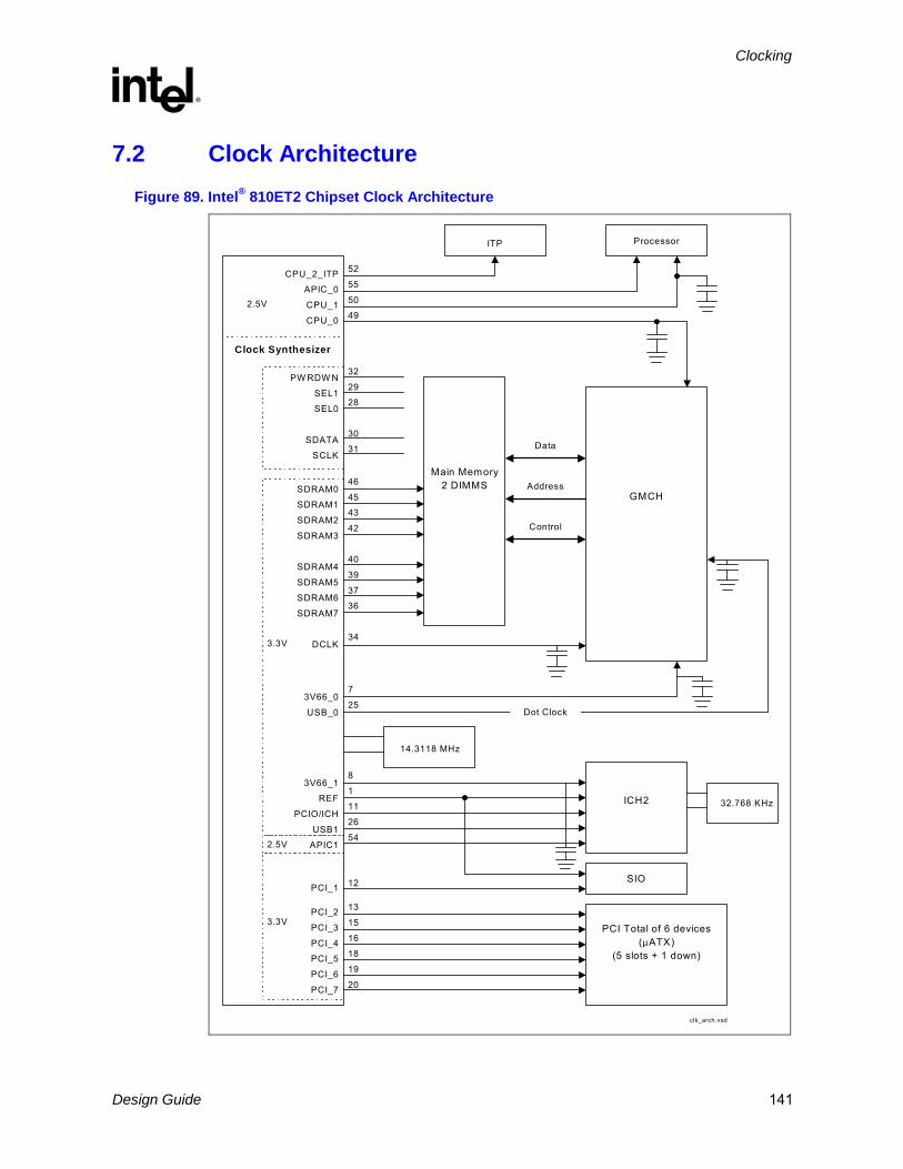
Clocking
R
Design Guide 141
7.2 Clock Architecture Figure 89. Intel® 810ET2 Chipset Clock Architecture
clk_arch.vsd
52
55
5049
CPU_2_ITPAPIC_0
CPU_1
CPU_0
2.5V
Clock Synthesizer
PW RDW N
SEL1SEL0
SDATASCLK
SDRAM0SDRAM1
SDRAM2
SDRAM3
SDRAM4
SDRAM5SDRAM6
SDRAM7
DCLK
32
2928
3031
46
4543
42
40
39
3736
34
Main Memory2 DIMMS
ITP Processor
GMCH
Data
Address
Control
3.3V
3V66_0
USB_0
14.3118 MHz
7
25
3V66_1REF
PCIO/ICH
USB1APIC1
8
111
26
54
ICH2
SIO
PCI Total of 6 devices(µATX)
(5 slots + 1 down)
32.768 KHz
Dot Clock
12PCI_1
13
15
1618
19
20
PCI_2
PCI_3
PCI_4PCI_5
PCI_6
PCI_7
2.5V
3.3V

Clocking
R
142 Design Guide
7.3 Clock Routing Guidelines Table 39 shows the group skew and jitter limits.
Table 39. Group Skew and Jitter Limits at the Pins of the Clock Chip
Signal Group Pin-Pin Skew Cycle-Cycle Jitter Nominal Vdd Skew, Jitter Measure Point
Processor 175 ps 250 pS 2.5V 1.25V
SDRAM 250 ps 250 pS 3.3V 1.50V
APIC 250 ps 500 pS 2.5V 1.25V
48 MHz 250 ps 500 pS 3.3V 1.50V
3V66 175 ps 500 pS 3.3V 1.50V
PCI 500 ps 500 pS 3.3V 1.50V
REF N/A 1000 pS 3.3V 1.50V
Table 40 shows the signal group and resistor tolerance.
Table 40. Signal Group and Resistor
Signal Group Resistor
Processor 33 Ω ± 5%
SDRAM 22 Ω ± 5%
DCLK 33 Ω ± 5%
3V66 22 Ω ± 5%
PCI 33 Ω ± 5%
TCLK 22 Ω ± 5%
OCLK/RCLK 33 Ω ± 5%
48 MHz 33 Ω ± 5%
APIC 33 Ω ± 5%
REF 10 Ω ± 5%
Table 41 shows the layout dimensions for the clock routing.
Note: All the clock signals must be routed on the same layer which reference to a ground plane.

Clocking
R
Design Guide 143
Table 41. Layout Dimensions
Group Receiver Resistor Cap Topology A B C D
MCLK DIMM 22 Ω N/A Layout 1 0.5 X N/A N/A
Processor: Intel® Pentium® III FC-PGA Processor 100/133 MHz
Segment C => Pentium III FC-PGA Processor
Segment D => GMCH
33 Ω N/A Layout 5 0.1 0.5 X+4.8" X+7.1
Processor: Intel® Celeron® processor 66/100 MHz
Segment C => Celeron processor socket
Segment D => GMCH
33 Ω N/A Layout 5 0.1 0.5 X+5.4" X+7.1
DCLK GMCH 33 Ω 22 pF Layout 3 0.5 X+3.2 0.5 N/A
3V66 GMCH 22 Ω 18 pF Layout 3 0.5 X+1.4 0.5 N/A
3V66 Intel® ICH2 22 Ω 18 pF Layout 3 0.5 X+1.4 0.5 N/A
PCI PCI device 33 Ω N/A Layout 1 0.5 X+3.0 to X+9.3
N/A N/A
PCI PCI socket 33 Ω N/A Layout 4 0.5 X+0.0 to X+6.0
N/A N/A
PCI ICH2 33 Ω N/A Layout 1 0.5 X+4.4 N/A N/A
TCLK SDRAM 22 Ω N/A Layout 6 0.5 1.5 to 2.5 0.75 to 1.25
N/A
OCLK/RCLK GMCH 33 Ω N/A Layout 1 0.5 3.25 to 3.75
N/A N/A
APIC PPGA 33 Ω N/A Layout 4 0.5 Y N/A N/A
APIC ICH2 33 Ω N/A Layout 1 0.5 Y+2.4 N/A N/A
NOTES: 1. W, X, Y and Z trace lengths are arbitrary. Below are some suggested values:
X=5.0 inches, Y=4.2 inches.
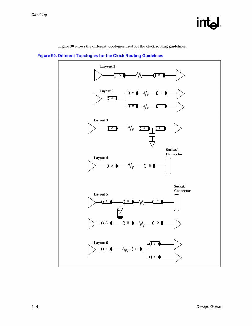
Clocking
R
144 Design Guide
Figure 90 shows the different topologies used for the clock routing guidelines.
Figure 90. Different Topologies for the Clock Routing Guidelines
Layout 1
BA
Layout 2 B C
A
B D
Layout 4
Socket/Connector
Socket/Connector
Layout 3
A B
CBA
Layout 5
B C
A
A
B DA
Layout 6B
C
A
C

Clocking
R
Design Guide 145
7.4 Capacitor Sites Intel recommends 0603 package capacitor sites placed as close as possible to the clock input receivers for AC tuning for the following signal groups:
• GMCH • Processor • SDRAM/DCLK • 3V66 • 3V66 to the ICH2
Figure 91. Example of Capacitor Placement Near Clock Input Receiver
7.5 Clock Power Decoupling Guidelines Several general layout guidelines should be followed when laying out the power planes for the CK810E clock generator.
• Isolate power planes to the each of the clock groups. • Place local decoupling as close to power pins as possible and connect with short, wide traces
and copper. • Connect pins to appropriate power plane with power vias (larger than signal vias). • Bulk decoupling should be connected to plane with 2 or more power vias. • Minimize clock signal routing over plane splits. • Do not route any signals underneath the clock generator on the component side of the board. • An example signal via is a 14 mil finished hole with a 24–26 mil path. An example power via
is an 18 mil finished hole with a 33–38 mil path. For large decoupling or power planes with large current transients it is recommended to use a larger power via.

Clocking
R
146 Design Guide
An example of clock power layout is presented in Figure 92.
Figure 92. Example of Clock Power Plane Splits and Decoupling
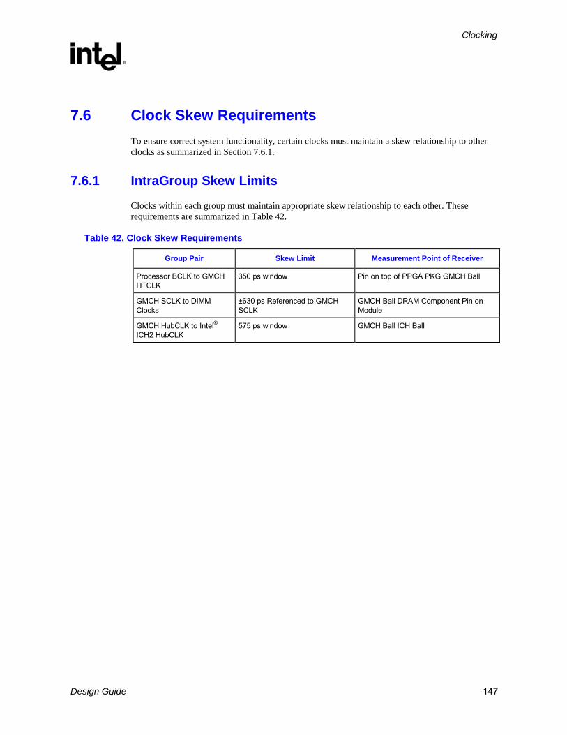
Clocking
R
Design Guide 147
7.6 Clock Skew Requirements To ensure correct system functionality, certain clocks must maintain a skew relationship to other clocks as summarized in Section 7.6.1.
7.6.1 IntraGroup Skew Limits
Clocks within each group must maintain appropriate skew relationship to each other. These requirements are summarized in Table 42.
Table 42. Clock Skew Requirements
Group Pair Skew Limit Measurement Point of Receiver
Processor BCLK to GMCH HTCLK
350 ps window Pin on top of PPGA PKG GMCH Ball
GMCH SCLK to DIMM Clocks
±630 ps Referenced to GMCH SCLK
GMCH Ball DRAM Component Pin on Module
GMCH HubCLK to Intel® ICH2 HubCLK
575 ps window GMCH Ball ICH Ball

Clocking
R
148 Design Guide
This page is intentionally left blank.

Power Delivery
R
Design Guide 149
8 Power Delivery This chapter contains power delivery guidelines. Table 43 provides definitions for power delivery terms used in this chapter.
Table 43. Power Delivery Definitions
Term Description
Suspend-To-RAM (STR)
In the STR state, the system state is stored in main memory and all unnecessary system logic is turned off. Only main memory and logic required to wake the system remain powered. This state is used in the Customer Reference Board (CRB) to satisfy the S3 ACPI power management state.
Full-power operation
During full-power operation, all components on the motherboard remain powered. Note that full-power operation includes both the full-on operating state and the S1 (CPU stop-grant state) state.
Suspend operation During suspend operation, power is removed from some components on the motherboard. The CRB supports two suspend states: Suspend-to-RAM (S3) and Soft-off (S5).
Power rails An ATX power supply has 6 power rails: +5V, -5V, +12V, -12V, +3.3V, 5VSB. In addition to these power rails, several other power rails are created with voltage regulators on the CRB.
Core power rail A power rail that is only on during full-power operation. These power rails are on when the PSON signal is asserted to the ATX power supply. The core power rails that are distributed directly from the ATX power supply are: ± 5V, ±12V and +3.3V.
Standby power rail A power rail that in on during suspend operation (these rails are also on during full-power operation). These rails are on at all times (when the power supply is plugged into AC power). The only standby power rail that is distributed directly from the ATX power supply is: 5VSB (5V Standby). There are other standby rails that are created with voltage regulators on the motherboard.
Derived power rail A derived power rail is any power rail that is generated from another power rail. For example, 3.3VSB is usually derived (on the motherboard) from 5VSB using a voltage regulator (on the CRB, 3.3VSB is derived from 5V_DUAL).
Dual power rail A dual power rail is derived from different rails at different times (depending on the power state of the system). Usually, a dual power rail is derived from a standby supply during suspend operation and derived from a core supply during full-power operation. Note that the voltage on a dual power rail may be misleading.
Figure 93 shows the power delivery architecture for an example 810E2 chipset universal platform-based system. This power delivery architecture supports the “Instantly Available PC Design Guidelines” via the suspend-to-RAM (STR) state. During STR, only the necessary devices are powered. These devices include: main memory, the ICH2 resume well, PCI wake devices (via 3.3 Vaux), AC’97, and optionally USB. (USB can be powered only if sufficient standby power is available.) To ensure that enough power is available during STR, a thorough power budget should be completed. The power requirements should include each device’s power requirements, both in suspend and in full power. The power requirements should be compared with the power budget supplied by the power supply. Due to the requirements of main memory and the PCI 3.3 Vaux (and possibly other devices in the system), it is necessary to create a dual power rail.
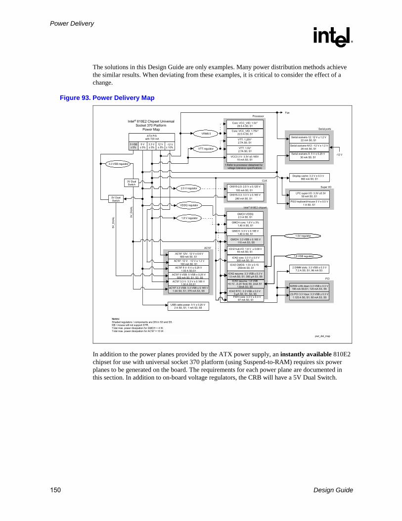
Power Delivery
R
150 Design Guide
The solutions in this Design Guide are only examples. Many power distribution methods achieve the similar results. When deviating from these examples, it is critical to consider the effect of a change.
Figure 93. Power Delivery Map
Intel® 810E2 Chipset UniversalSocket 370 Platform
Power MapVRM8.5
ProcessorFan
-12 VSerial xceivers-5: 5 V ± 0.25 V30 mA S0, S1
Serial xceivers-12: 12 V ± 1.2 V22 mA S0, S1
Serial xceivers-N12: -12 V ± 1.2 V28 mA S0, S1
Serial ports
Intel® 810E2 chipset
VTT regulator
Display cache: 3.3 V ± 0.3 V960 mA S0, S1
CK815-3.3: 3.3 V ± 0.165 V280 mA S0, S1
CK815-2.5: 2.5 V ± 0.125 V100 mA S0, S1
CLK
2.5 V regulator
1.8 V regulator
AC'97
3.3 VSB regulator
ATX P/Swith 720 mA
5 VSB± 5%
12 V± 5%
3.3 V± 5%
5 V± 5%
-12 V± 10%
LPC super I/O: 3.3V ±0.3V50 mA S0, S1
PS/2 keyboard/mouse 5 V ± 0.5 V1 A S0, S1
Super I/O
2 DIMM slots: 3.3 VSB ± 0.3 V7.2 A S0, S1; 96 mA S3
(3) PCI 3.3 Vaux: 3.3 VSB ± 0.3 V1.125 A S0, S1; 60 mA S3, S5
82559 LAN down 3.3 VSB ± 0.3 V195 mA S0,S1; 120 mA S3, S5
PCI
3V_D
UAL
GMCH: 3.3 VSB ± 0.165 V110 mA S3, S5
GMCH core: 1.8 V ± 3%1.40 A S0, S1
GMCH: 3.3 V ± 0.165 V1.40 A S0, S1
FWH core: 3.3 V ± 0.3 V67 mA S0, S1
ICH2 resume: 3.3 VSB ± 0.3 V1.5 mA S0, S1; 300 µA S3, S5
+0.1V, -0.2V 5mA S0, 2mA S1
ICH2 core: 3.3 V ± 0.3 V300 mA S0, S1
ICH2 hub I/O: 1.8 V ± 0.09 V55 mA S0, S1
pwr_del_map
AC'97 3.3 VSB: 3.3 VSB ± 0.165 V1.0A S0, S1; 375 mA S3, S5
AC'97 12V: 12 V ± 0.6 V 500 mA S0, S1
AC'97 -12 V: -12 V ± 1.2 V100 mA S0, S1
AC'97 5 V: 5 V ± 0.25 V1.00 A S0,S1
AC'97 5 VSB: 5 VSB ± 0.25 V500 mA S0, S1, S3, S5
AC'97 3.3 V: 3.3 V ± 0.165 V1.00 A S0,S1
Notes:Shaded regulators / components are ON in S3 and S5.KB / mouse will not support STR.Total max. power dissipation for GMCH = 4 W.Total max. power dissipation for AC'97 = 15 W.
VDDQ regulator
GMCH VDDQ2.3 A S0, S1
3V DualSwitch
5V DualSwitch
5V_D
UAL
VCC3.3 V: 3.3V ±0.165V15 mA S0, S1
VTT: 1.5V1
2.7A S0, S1
VTT: 1.25V1
2.7A S0, S1
Core: VCC_VID: 1.75V1
22.0 A S0, S1
Core: VCC_VID: 1.5V1
28.5 A S0, S1
1 Refer to processor datasheet for voltage tolerance specifications
USB cable power: 5 V ± 0.25 V2 A S0, S1; 1 mA S3, S5
ICH2 RTC: 3.3 VSB ± 0.3 V5 µA S0, S1, S3, S5
ICH2 resume: 1.8 VSB
1.8mA S3, S5
250mA S0, S1ICH2 CMOS: 1.5V ± 0.15
1.5V regulator
1.8 VSB regulator
In addition to the power planes provided by the ATX power supply, an instantly available 810E2 chipset for use with universal socket 370 platform (using Suspend-to-RAM) requires six power planes to be generated on the board. The requirements for each power plane are documented in this section. In addition to on-board voltage regulators, the CRB will have a 5V Dual Switch.
Power Delivery
R
Design Guide 151
5V Dual Switch
This switch will power the 5V Dual plane from the 5V core ATX supply during full-power operation. During Suspend-to-RAM, the 5V Dual plane will be powered from the 5V Standby power supply. Note: the voltage on the 5V Dual plane is not 5V! There is a resistive drop through the 5V Dual Switch that must be considered. Therefore, NO COMPONENTS should be connected directly to the 5V Dual plane. On the CRB, the only devices connected to the 5V Dual plane are voltage regulators (to regulate to lower voltages).
Note: This switch is not required in an Intel 810E2 chipset for use with universal socket 370 platform that does not support Suspend-to-RAM (STR).
VTT
This power plane is used to power the AGTL/AGTL+ termination resistors. Refer to the latest revisions of the Pentium III processor (CPUID=068xh) and Celeron processor (CPUID=068xh) datasheets.
Note: This regulator is required in ALL designs.
1.8V
The 1.8V plane powers the GMCH core and the ICH2 hub interface I/O buffers. This power plane has a total power requirement of approximately 1.7A. The 1.8V plane should be decoupled with a 0.1 µF and a 0.01 µF chip capacitor at each corner of the GMCH and with a single 1 µF and 0.1 µF capacitor at the ICH2.
Note: This regulator is required in ALL designs.
VDDQ
The VDDQ plane is used to power the GMCH AGP interface and the graphics component AGP interface. Refer to the AGP Interface Specification Revision 2.0 (http://www.agpforum.org) and ECR#43 and ECR#44 for specific VDDQ delivery requirements.
For the consideration of component long-term reliability, the following power sequence is strongly recommended while the AGP interface of GMCH is running at 3.3V. If the AGP interface is running at 1.5V, the following power sequence recommendation is no longer applicable. The power sequence recommendations are:
• During the power-up sequence, the 1.8V must ramp up to 1.0V Before 3.3V ramps up to 2.2V
• During the powerdown sequence, the 1.8V CAN NOT ramp below 1.0V Before 3.3V ramps below 2.2V
• The same power sequence recommendation also applies to the entrance and exit of S3 state, since MCH power is compete off during the S3 state.
Refer to Section 8.3.2 for more information on the power ramp sequence requirement between 3.3V and 1.8V. System designers need to be aware of this requirement while designing the voltage regulators and selecting the power supply. For further details on the voltage sequencing

Power Delivery
R
152 Design Guide
requirements, refer to the Intel® 810 Chipset Family: 82810 Graphics and Memory Controller Hub (GMCH) Datasheet.
3.3VSB
The 3.3VSB plane powers the I/O buffers in the resume well of the ICH2 and the PCI 3.3Vaux suspend power pins. The 3.3Vaux requirement state that during suspend, the system must deliver 375 mA to each wake-enabled card and 20 mA to each non wake-enabled card. During full-power operation, the system must be able to supply 375 mA to each card. Therefore, the total current requirement is:
• Full-power Operation: 375 mA * number of PCI slots
• Suspend Operation: 375 mA + 20 mA * (number of PCI slots – 1)
In addition to the PCI 3.3Vaux, the ICH2 suspend well power requirements must be considered as shown in Figure 93.
Note: This regulator is required in ALL designs.
1.8VSB
The 1.8VSB plane powers the logic to the resume well of the ICH2. This should not be used for VCMOS.
8.1 Thermal Design Power The Thermal Design power (TDP) is defined as the estimated maximum possible expected power generated in a component by a realistic application. It is based on extrapolations in both hardware and software technology over the life of the product. It does not represent the expected power generated by a power virus.
The TDP of the 82810E2 GMCH component is 5.1W.
The TDP of the 82801BA ICH2 is 1.5 W ±15%.

Power Delivery
R
Design Guide 153
8.1.1 Pull-Up and Pull-Down Resistor Values
The pull-up and pull-down values are system dependent. The appropriate value for a system can be determined from an AC/DC analysis of the pull-up voltage used, the current drive capability of the output driver, the input leakage currents of all devices on the signal net, the pull-up voltage tolerance, the pull-up/pull-down resistor tolerance, the input high-voltage/low-voltage specifications, the input timing specifications (RC rise time), etc. Analysis should be performed to determine the minimum/maximum values usable on an individual signal. Engineering judgment should be used to determine the optimal value. This determination can include cost concerns, commonality considerations, manufacturing issues, specifications, and other considerations.
A simplistic DC calculation for a pull-up value is:
RMAX = (VccPU MIN - VIH MIN) / ILEAKAGE MAX
RMIN = (VccPU MAX - VIL MAX) / IOL MAX
Since ILEAKAGE MAX is normally very small, RMAX may not be meaningful. RMAX also is determined by the maximum allowable rise time. The following calculation allows for t, the maximum allowable rise time, and C, the total load capacitance in the circuit, including the input capacitance of the devices to be driven, the output capacitance of the driver, and the line capacitance. This calculation yields the largest pull-up resistor allowable to meet the rise time t.
RMAX = -t / (C * In(1-(VIH MIN / VccPU MIN) ) )
Figure 94. Pull-Up Resistor Example
Vccpu min.
Rmax
VIH min.ILeakage max.
Vccpu max.
Rmin
VIL max.IOL max.
pwr_pullup_res
8.2 ATX Power Supply PWRGOOD Requirements The PWROK signal must be glitch free for proper power management operation. The ICH2 sets the PWROK_FLR bit (ICH2 GEN_PMCON_2, General PM Configuration 2 Register, PM-dev31: function 0, bit 0, at offset A2h). If this bit is set upon resume from S3 powerdown, the system will reboot and control of the system will not be given to the program running when entering the S3 state. System designers should insure that PWROK signal designs are glitch free.

Power Delivery
R
154 Design Guide
8.3 Power Management Signals • A power button is required by the ACPI specification.
• PWRBTN# is connected to the front panel on/off power button. The ICH2 integrates 16 ms debouncing logic on this pin.
• AC power loss circuitry has been integrated into the ICH2 to detect power failure.
• It is recommended that the ATXPWROK signal from the power supply connector be routed through a Schmitt trigger to square off and maintain its signal integrity. It should not be connected directly to logic on the board.
• PWROK logic from the power supply connector can be powered from the core voltage supply.
• RSMRST# logic should be powered by a standby supply, while making sure that the input to the ICH2 is at the 3 V level. The RSMST# signal requires a minimum time delay of 1 ms from the rising edge of the standby power supply voltage. A Schmitt trigger circuit is recommended to drive the RSMRST# signal. To provide the required rise time, the 1 ms delay should be placed before the Schmitt trigger circuit. The reference design implements a 20 ms delay at the input of the Schmitt trigger to ensure that the Schmitt trigger inverters have sufficiently powered up before switching the input. Also, ensure that voltage on RSMRST# does not exceed VCC (RTC).
• It is recommended that 3.3 V logic be used to drive RSMRST# to alleviate rise time problems when using a resistor divider from VCC5.
• The PWROK signal to the chipset is a 3 V signal.
• The core well power valid to PWROK asserted at the chipset is a minimum of 1 ms.
• PWROK to the chipset must be deasserted after RSMRST#.
• PWRGOOD signal to processor is driven with an open-collector buffer pulled up to 2.5 V, using a 330 Ω resistor.
• RI# can be connected to the serial port if this feature is used. To implement ring indicate as a wake event, the RS232 transceiver driving the RI# signal must be powered when the ICH2 suspend well is powered. This can be achieved with a serial port transceiver powered from the standby well that implements a shutdown feature.
• SLP_S3# from the ICH2 must be inverted and then connected to PSON of the power supply connector to control the state of the core well during sleep states.
• For an ATX power supply, when PSON is Low, the core wells are turned on. When PSON is high, the core wells from the power supply are turned off.
Power Delivery
R
Design Guide 155
8.3.1 Power Button Implementation
The following items should be considered when implementing a power management model for a desktop system. The power states are as follows:
S1 – Stop Grant – (processor context not lost)
S3 – STR (Suspend to RAM)
S4 – STD (Suspend to Disk)
S5 – Soft-off
• Wake: Pressing the power button wakes the computer from S1–S5.
• Sleep: Pressing the power button signals software/firmware in the following manner:
• If SCI is enabled, the power button will generate an SCI to the OS. The OS will implement the power button policy to allow orderly shutdowns. Do not override this with additional hardware.
• If SCI is not enabled: Enable the power button to generate an SMI and go directly to soft-off or a supported
sleep state. Poll the power button status bit during POST while SMIs are not loaded and go directly
to soft-off if it gets set. Always install an SMI handler for the power button that operates until ACPI is enabled.
• Emergency Override: Pressing the power button for 4 seconds goes directly to S5. This is only to be used in EMERGENCIES when system is not responding. This will cause the user data to be lost in most cases.
• Do not promote pressing the power button for 4 seconds as the normal mechanism to power the machine off. This violates ACPI.
• To be compliant with the latest PC9x specification, machines must appear to the user to be off when in the S1–S4 sleeping states. This includes: All lights, except a power state light, must be off. The system must be inaudible: silent or stopped fan, drives off.
Note: Contact Microsoft for the latest information concerning PC9x and Microsoft Logo programs.
8.3.2 1.8V/3.3V Power Sequencing
The ICH2 has two pairs of associated 1.8V and 3.3V supplies. These are VCC1.8, VCC3.3 and VCCSus1_8, VCCSus3_3. These pairs are assumed to power up and power down together. The difference between the two associated supplies must never be greater than 2.0V. The 1.85V supply may come up before the 3.3V supply without violating this rule (though this is generally not practical in a desktop environment, since the 1.8V supply is typically derived from the 3.3V supply by means of a linear regulator).
One serious consequence of violation of this "2V Rule" is electrical overstress of oxide layers, resulting in component damage.

Power Delivery
R
156 Design Guide
The majority of the ICH2 I/O buffers are driven by the 3.3V supplies, but are controlled by logic that is powered by the 1.8V supplies. Thus, another consequence of faulty power sequencing arises if the 3.3V supply comes up first. In this case the I/O buffers will be in an undefined state until the 1.8V logic is powered up. Some signals that are defined as "Input-only" actually have output buffers that are normally disabled, and the ICH2 may unexpectedly drive these signals if the 3.3V supply is active while the 1.8V supply is not.
Figure 95 shows an example power-on sequencing circuit that ensures the “2V Rule” is obeyed. This circuit uses a NPN (Q2) and PNP (Q1) transistor to ensure the 1.8V supply tracks the 3.3V supply. The NPN transistor controls the current through PNP from the 3.3V supply into the 1.8V power plane by varying the voltage at the base of the PNP transistor. By connecting the emitter of the NPN transistor to the 1.8V plane, current will not flow from the 3.3V supply into 1.8V plane when the 1.8V plane reaches 1.8V.
Figure 95. Example 1.8V/3.3V Power Sequencing Circuit
Q1 PNP
Q2 NPN
220
220
470
+3.3V +1.8V
When analyzing systems that may be "marginally compliant" to the 2V Rule, please pay close attention to the behavior of the ICH2's RSMRST# and PWROK signals, since these signals control internal isolation logic between the various power planes:
• RSMRST# controls isolation between the RTC well and the Resume wells.
• PWROK controls isolation between the Resume wells and Main wells
If one of these signals goes high while one of its associated power planes is active and the other is not, a leakage path will exist between the active and inactive power wells. This could result in high, possibly damaging, internal currents.

Power Delivery
R
Design Guide 157
8.3.3 3.3V/V5REF Sequencing
V5REF is the reference voltage for 5V tolerance on inputs to the ICH2. V5REF must be powered up before or simultaneously to VCC3.3. It must also power down after or simultaneous to VCC3.3. The rule must be followed in order to ensure the safety of the ICH2. If the rule is violated, internal diodes will attempt to draw power sufficient to damage the diodes from the VCC3.3 rail. Figure 96 shows a sample implementation of how to satisfy the V5REF/3.3V sequencing rule.
As an additional consideration, during suspend, the only signals that are 5V tolerant capable are USB OC:[3:0]#. If these signals are not needed during suspend, V5REF_SUS can be connected to either VccSus3_3 or 5V_Always/5V_AUX. If OC:[3:0]# is needed during suspend and 5V tolerance is required then V5REF_SUS should be connected to 5V_Always/5V_AUX, but if 5V tolerance is not needed in suspend, then V5REF_SUS can be connected to either VccSus3_3 or 5V_Always/5V_AUX rails.
Figure 96. 3.3V/V5REF Sequencing Circuitry
Vcc Supply(3.3 V)
1 KΩ
5V Supply
1 µF
To System VREF To System
3.3V_5V_Seq_Ckt

Power Delivery
R
158 Design Guide
8.4 Power Plane Splits Figure 97. Power Plane Split Example
pwr_plane_splits
8.5 Power_Supply PS_ON Considerations - If a pulse on SLP_S3# or SLP_S5# is short enough (~ 10-100mS) such that PS_ON is driven
active during the exponential decay of the power rails, a few power supplies may not be designed to handle this short pulse condition. In this case, the power supply will not respond to this event and never power back up. These power supplies would need to be unplugged and re-plugged to bring the system back up. Power supplies not designed to handle this condition must have their power rails decay to a certain voltage level before they can properly respond to PS_ON. This level varies with affected power supply.
- The ATX spec does not specify a minimum pulse width on PS_ON de-assertion, which means power supplies must be able to handle any pulse width. This issue can affect any power supply (beyond ATX) with similar PS_ON circuitry. Due to variance in the decay of the core power rails per platform, a single board or chipset silicon fix would be non-deterministic (may not solve the issue in all cases).
- The platform designer must ensure that the power supply used with the platform is not affected by this issue.

Design Checklist
R
Design Guide 159
9 Design Checklist
9.1 Design Review Checklist This checklist highlights design considerations that should be reviewed prior to manufacturing a motherboard that implements an 810E2 chipset universal socket 370 platform. This is not a complete list and does not guarantee that a design will function properly. Beyond the items contained in the following text, refer to the most recent version of the Design Guide for more detailed instructions on designing a motherboard.
9.1.1 Design Checklist Summary
The following tables provide design considerations for the various portions of a design. Each table describes one of those portions, and is titled accordingly. Contact your Intel Field Representative for questions or issues regarding interpretation of the information contained in these tables.
Table 44. AGTL+ Connectivity Checklist for 370-Pin Socket Processors
Processor Pin I/O Recommendations
A[35:3]# 1 I/O • Connect A[31:3]# to GMCH. Leave A[35:32]# as No Connect (not supported by chipset).
ADS# 1 I/O • Connect to GMCH.
AERR# I/O • Leave as No Connect (not supported by chipset).
AP[1:0]# I/O • Leave as No Connect (not supported by chipset).
BERR# I/O • Leave as No Connect (not supported by chipset).
BINIT# I/O • Leave as No Connect (not supported by chipset).
BNR# 1 I/O • Connect to GMCH.
BP[3:2]# I/O • Leave as No Connect.
BPM[1:0] I/O • Leave as No Connect.
BPRI# 1 I • Connect to GMCH.
BREQ[0]# (BR0#) I/O • 10 Ω pull-down resistor to ground.
D[63:0]# 1 I/O • Connect to GMCH.
DBSY# 1 I/O • Connect to GMCH.
DEFER# 1 I • Connect to GMCH.
DEP[7:0]# I/O • Leave as No Connect (not supported by chipset).
DRDY# 1 I/O • Connect to GMCH.
HIT# 1 I/O • Connect to GMCH.
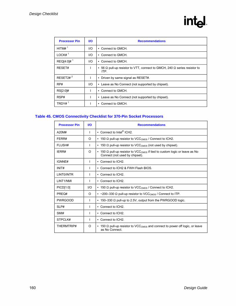
Design Checklist
R
160 Design Guide
Processor Pin I/O Recommendations
HITM# 1 I/O • Connect to GMCH.
LOCK# 1 I/O • Connect to GMCH.
REQ[4:0]# 1 I/O • Connect to GMCH.
RESET# I • 56 Ω pull-up resistor to VTT, connect to GMCH, 240 Ω series resistor to ITP.
RESET2# 2 I • Driven by same signal as RESET#.
RP# I/O • Leave as No Connect (not supported by chipset).
RS[2:0]# I • Connect to GMCH.
RSP# I • Leave as No Connect (not supported by chipset).
TRDY# 1 I • Connect to GMCH.
Table 45. CMOS Connectivity Checklist for 370-Pin Socket Processors
Processor Pin I/O Recommendations
A20M# I • Connect to Intel® ICH2.
FERR# O • 150 Ω pull-up resistor to VCCCMOS / Connect to ICH2.
FLUSH# I • 150 Ω pull-up resistor to VCCCMOS (not used by chipset).
IERR# O • 150 Ω pull-up resistor to VCCCMOS if tied to custom logic or leave as No Connect (not used by chipset).
IGNNE# I • Connect to ICH2.
INIT# I • Connect to ICH2 & FWH Flash BIOS.
LINT0/INTR I • Connect to ICH2.
LINT1/NMI I • Connect to ICH2.
PICD[1:0] I/O • 150 Ω pull-up resistor to VCCCMOS / Connect to ICH2.
PREQ# O • ~200330 Ω pull-up resistor to VCCCMOS / Connect to ITP.
PWRGOOD I • 150330 Ω pull-up to 2.5V, output from the PWRGOOD logic.
SLP# I • Connect to ICH2.
SMI# I • Connect to ICH2.
STPCLK# I • Connect to ICH2.
THERMTRIP# O • 150 Ω pull-up resistor to VCCCMOS and connect to power off logic, or leave as No Connect.

Design Checklist
R
Design Guide 161
Table 46. TAP Checklist for a 370-Pin Socket Processor
Processor Pin I/O Recommendations
TCK I • 39 Ω pull-down resistor to ground/ Connect to ITP.
TDI I • 200330 Ω pull-up resistor to VCCCMOS / Connect to ITP.
TDO O • 150 Ω pull-up resistor to VCCCMOS / Connect to ITP.
TMS I • 39 Ω pull-up resistor to VCCCMOS / 47 Ω series resistor to ITP.
TRST# I • 500-680 Ω pull-down resistor to ground / Connect to ITP.
PRDY# I • 150 Ω pull-up resistor to VTT / 240 Ω series resistor to ITP.
NOTES: 1. The ITP connector is different than the one previously specified for other Intel IA-32 processors. It is the
female counterpart to the previously specified connector and is specifically for use with processors utilizing 1.5V CMOS TAP I/O signals.
2. The Pentium III processor requires an ITP with a 1.5V tolerant buffer board. Previous ITPs are designed to work higher voltages and may damage the processor if they are connected to a Pentium III processor.
Table 47. Miscellaneous Checklist for 370-Pin Socket Processors
Processor Pin I/O Recommendations
BCLK I • Connect to clock generator / 2233 Ω series resistor (though OEM needs to simulate based on driver characteristics). To reduce pin-to-pin skew, tie host clock outputs together at the clock driver then route to the GMCH and processor.
BSEL0 I/O • Case 1, 66/100/133 MHz support: 1 kΩ pull-up resistor to 3.3V, connect to CK810E SEL0 input, connect to GMCH LMD29 pin via 10 kΩ series resistor.
• Case 2, 100/133 MHz support: 1 kΩ pull-up resistor to 3.3V, connect to PWRGOOD logic such that a logic low on BSEL0 negates PWRGOOD.
BSEL1 I/O • 1 kΩ pull-up resistor to 3.3V, connect to CK810E REF pin via 10 kΩ series resistor, connect to GMCH LMD13 pin via 10 kΩ series resistor.
CLKREF I • Connect to divider on VCC2.5 or VCC3.3 to create 1.25V reference with a 4.7 µF decoupling capacitor. Resistor divider must be created from 1% tolerance resistors. Do not use VTT as source voltage for this reference!
CPUPRES# • Tie to ground, leave as No Connect, or could be connected to PWRGOOD logic to gate system from powering on if no processor is present. If used, 1 kΩ10 kΩ pull-up resistor to any voltage.
EDGCTRL I • 51 Ω ±5% pull-up resistor to VCCCORE.
PICCLK I • Connect to clock generator / 2233 Ω series resistor (though OEM needs to simulate based on driver characteristics).
PLL1, PLL2 I • Low pass filter on VCCCORE provided on motherboard. Typically a 4.7 uH inductor in series with VCCCORE is connected to PLL1 then through a series 33 µF capacitor to PLL2.
RTTCTRL51 (S35)
• 110 Ω ±1% pull-down resistor to ground.
SLEWCTRL (E27)
• 110 Ω ±1% pull-down resistor to ground.

Design Checklist
R
162 Design Guide
Processor Pin I/O Recommendations
THERMDN O • No Connect if not used; otherwise connect to thermal sensor using vendor guidelines.
THERMDP I • No Connect if not used; otherwise connect to thermal sensor using vendor guidelines.
VCC1.5 I • Connected to same voltage source as VTT. Must have some high and low frequency decoupling.
VCC2.5 I • Connected to 2.5V voltage source. Should have some high and low frequency decoupling.
VCCCMOS O • Used as pull-up voltage source for CMOS signals between processor and chipset and for TAP signals between processor and ITP. Must have some decoupling (HF/ LF) present.
VCCCORE I • 10 ea (min) 4.7 µF in 1206 package all placed within the PGA370 socket cavity.
• 8 ea (min) 1 µF in 0612 package placed in the PGA370 socket cavity.
VCOREDET (E21)
O • For the Intel® Celeron® processor (CPUID=068xh), Intel® Pentium® III processor (CPUID=068xh), and future 0.13 micron socket 370 processors, VCOREDET must float.
VID[3:0] O • Connect to on-board VR or VRM. For on-board VR, 10 kΩ pull-up resistor to power-solution compatible voltage required (usually pulled up to input voltage of the VR). Some of these solutions have internal pull-ups. Optional override (jumpers, ASIC, etc.) could be used. May also connect to system monitoring device.
VID[4] N/A • Connect regulator controller pin to ground (not on processor).
VREF[7:0] I • Connect to VREF voltage divider made up of 75 Ω and 150 Ω 1% resistors connected to VTT.
• Decoupling Guidelines:
• Four ea. (min) 0.1 µF in 0603 package placed within 500 mils of VREF pins.
VTT I • Connect AH20, AK16, AL13, AL21, AN11, AN15, and G35 to 1.5V regulator. Provide high and low frequency decoupling.
• Decoupling Guidelines: 19 ea (min) 0.1 µF in 0603 package placed within 200 mils of
AGTL+ termination resistor packs (r-paks). Use one capacitor for every two (r-paks).
4 ea (min) 0.47 µF in 0612 package
Additional VTT I • AA33, AA35, AN21, E23, S33, S37, U35, U37
GND N/A • AJ3
No Connects N/A • The following pins must be left as no-connects: AK30, AM2, F10, G37, L33, N33, N35, N37, Q33, Q35, Q37, R2, W35, X2, Y1
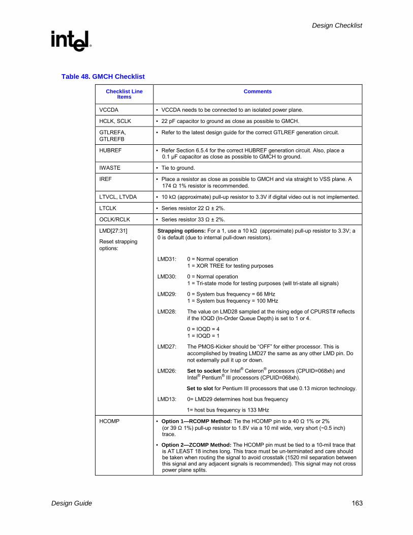
Design Checklist
R
Design Guide 163
Table 48. GMCH Checklist
Checklist Line Items
Comments
VCCDA • VCCDA needs to be connected to an isolated power plane.
HCLK, SCLK • 22 pF capacitor to ground as close as possible to GMCH.
GTLREFA, GTLREFB
• Refer to the latest design guide for the correct GTLREF generation circuit.
HUBREF • Refer Section 6.5.4 for the correct HUBREF generation circuit. Also, place a 0.1 µF capacitor as close as possible to GMCH to ground.
IWASTE • Tie to ground.
IREF • Place a resistor as close as possible to GMCH and via straight to VSS plane. A 174 Ω 1% resistor is recommended.
LTVCL, LTVDA • 10 kΩ (approximate) pull-up resistor to 3.3V if digital video out is not implemented.
LTCLK • Series resistor 22 Ω ± 2%.
OCLK/RCLK • Series resistor 33 Ω ± 2%.
LMD[27:31]
Reset strapping options:
Strapping options: For a 1, use a 10 kΩ (approximate) pull-up resistor to 3.3V; a 0 is default (due to internal pull-down resistors).
LMD31: 0 = Normal operation 1 = XOR TREE for testing purposes
LMD30: 0 = Normal operation 1 = Tri-state mode for testing purposes (will tri-state all signals)
LMD29: 0 = System bus frequency = 66 MHz 1 = System bus frequency = 100 MHz
LMD28: The value on LMD28 sampled at the rising edge of CPURST# reflects if the IOQD (In-Order Queue Depth) is set to 1 or 4.
0 = IOQD = 4 1 = IOQD = 1
LMD27: The PMOS-Kicker should be OFF for either processor. This is accomplished by treating LMD27 the same as any other LMD pin. Do not externally pull it up or down.
LMD26: Set to socket for Intel® Celeron® processors (CPUID=068xh) and Intel® Pentium® III processors (CPUID=068xh).
Set to slot for Pentium III processors that use 0.13 micron technology.
LMD13: 0= LMD29 determines host bus frequency
1= host bus frequency is 133 MHz
HCOMP • Option 1—RCOMP Method: Tie the HCOMP pin to a 40 Ω 1% or 2% (or 39 Ω 1%) pull-up resistor to 1.8V via a 10 mil wide, very short (~0.5 inch) trace.
• Option 2—ZCOMP Method: The HCOMP pin must be tied to a 10-mil trace that is AT LEAST 18 inches long. This trace must be un-terminated and care should be taken when routing the signal to avoid crosstalk (1520 mil separation between this signal and any adjacent signals is recommended). This signal may not cross power plane splits.

Design Checklist
R
164 Design Guide
Table 49. System Memory Checklist
Checklist Line Items Recommendations
Pin 147 • Connect to Ground (since the Intel® 810E2 chipset does not support registered DIMMs).
WP (Pin 81 on the DIMMs)
• Add a 4.7 kΩ pull-up resistor to 3.3V. This is a recommendation to write-protect the DIMMs EEPROM.
MAA[7:4], MAB[7:4] • Add 10 Ω series resistors to the MAA[7:4], MAB[7:4] as close as possible to GMCH for signal integrity.
Table 50. Display Cache Checklist
Checklist Line Items Recommendations
CKE • 4.7 kΩ pull-up resistor to VCC3.
9.2 Intel® ICH2 Checklist
9.2.1 PCI Interface Checklist Items Recommendations
All • All inputs to the Intel® ICH2 must not be left floating. Many GPIO signals are fixed inputs that must be pulled up to different sources. See GPIO section for recommendations.
PERR#, SERR# PLOCK#, STOP# DEVSEL#, TRDY# IRDY#, FRAME# REQ#[0:4], GPIO[0:1], THRM#
• These signals require a pull-up resistor. Recommend an 8.2 Ω pull-up resistor to VCC3.3 or a 2.7 kΩ pull-up resistor to VCC5. See PCI 2.2 Component Specification for pull-up recommendations for VCC3.3 and VCC5.
PCIRST# • The PCIRST# signal should be buffered to form the IDERST# signal.
• 33 Ω series resistor to IDE connectors.
PCIGNT# • No external pull-up resistors are required on PCI GNT signals. However, if external pull-up resistors are implemented, they must be pulled up to VCC3.3.
PME# • No extra pull-up resistors. This signal has integrated pull-up resistors of 24 kΩ.
SERIRQ • External weak (8.2 kΩ) pull-up resistor to VCC3.3 is recommended.
GNT[A]# /GPIO[16], GNT[B]/ GNT[5]#/ GPIO[17]
• No extra pull-up needed. These signals have integrated pull-ups of 24 kΩ.
• GNT[A] has an added strap function of top block swap. The signal is sampled on the rising edge of PWROK. Default value is high or disabled due to pull-up. A Jumper to a pull-down resistor can be added to manually enable the function.

Design Checklist
R
Design Guide 165
9.2.2 Hub Interface Checklist Items Recommendations
HL[11] • No pull-up resistor required. Use a no-stuff or a test point to put the Intel® ICH2 into NAND chain mode testing
HL_COMP • Tie the COMP pin to a 40 Ω 1% or 2% (or 39 Ω - 1%) pull-up resistor (to VCC1.8) via a 10-mil wide, very short (~0.5 inch) trace. ZCOMP No longer supported.
9.2.3 LAN Interface Checklist
Items Recommendations Comments
1 • Trace Spacing: 5 mils wide, 10 mil spacing
2 • LAN Max Trace Length Intel® ICH2 to CNR: L = 3 inch to 9 inch (0.5 inch to 3 inches on card)
To meet timing requirements.
3 • Stubs due to R-pak CNR/LOM stuffing option should not be present.
To minimize inductance.
4 • Maximum Trace Lengths: ICH2 to Intel® 82562EH: L = 4.5 inches to 10 inches; Intel® 82562ET: L = 3.5 inches to 10 inches; Intel® 82562EM: L = 4.5 inches to 8.5 inches.
To meet timing requirements.
5 • Max mismatch between the length of a clock trace and the length of any data trace is 0.5 inch (clock must be longest trace)
To meet timing and signal quality requirements.
6 • Maintain constant symmetry and spacing between the traces within a differential pair out of the LAN phy.
To meet timing and signal quality requirements.
7 • Keep the total length of each differential pair under 4 inches.
Issues found with traces longer than 4 inches : IEEE phy conformance failures, excessive EMI and or degraded receive BER.
8 • Do not route the transmit differential traces closer than 100 mils to the receive differential traces.
To minimize crosstalk.
9
• Distance between differential traces and any other signal line is 100 mils. (300 mils recommended)
To minimize crosstalk.
10 • Route 5 mils on 7 mils for differential pairs (out of LAN phy)
To meet timing and signal quality requirements.
11 • Differential trace impedance should be controlled to be ~100 Ω s.
To meet timing and signal quality requirements.
12 • For high-speed signals, the number of corners and vias should be kept to a minimum. If a 90-degree bend is required, it is recommended to use two 45-degree bends.
To meet timing and signal quality requirements.
13 • Traces should be routed away from board edges by a distance greater than the trace height above the ground plane.
This allows the field around the trace to couple more easily to the ground plane rather than to adjacent wires or boards.
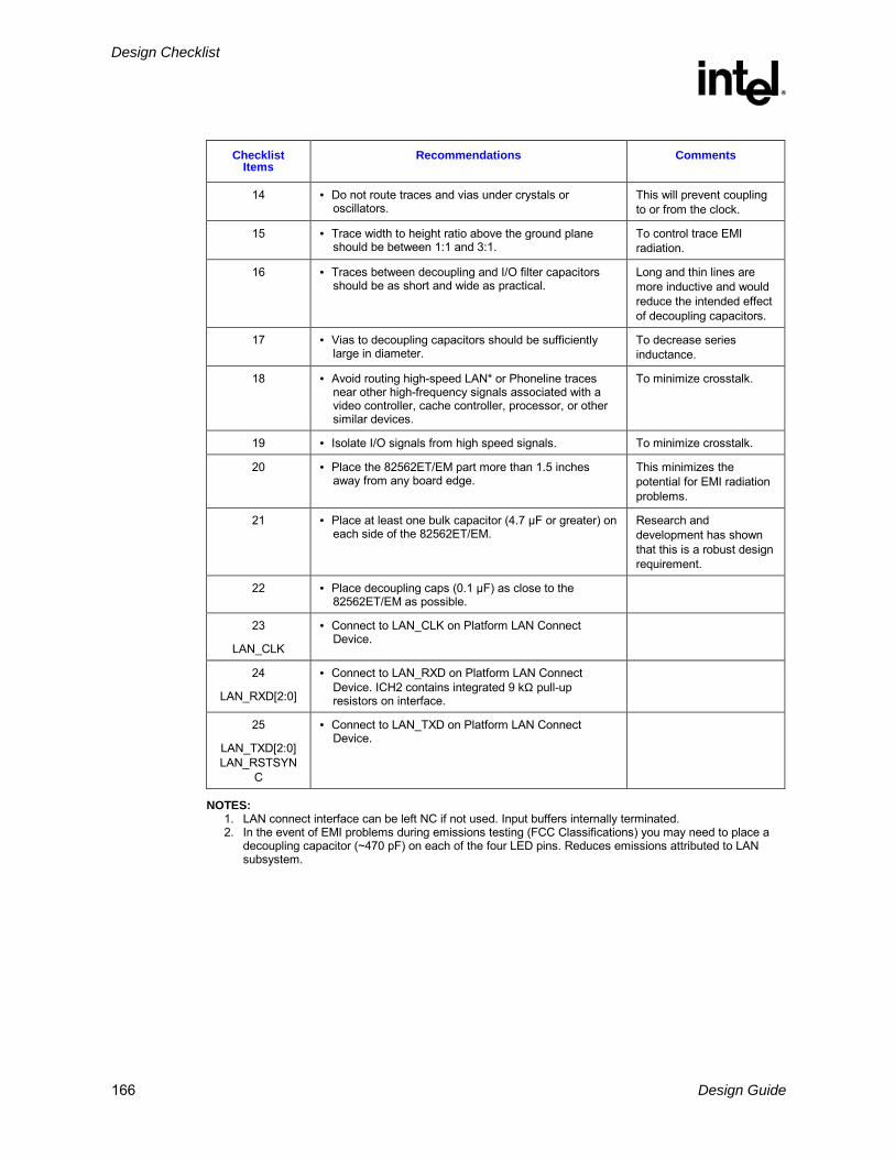
Design Checklist
R
166 Design Guide
Checklist Items
Recommendations Comments
14 • Do not route traces and vias under crystals or oscillators.
This will prevent coupling to or from the clock.
15 • Trace width to height ratio above the ground plane should be between 1:1 and 3:1.
To control trace EMI radiation.
16 • Traces between decoupling and I/O filter capacitors should be as short and wide as practical.
Long and thin lines are more inductive and would reduce the intended effect of decoupling capacitors.
17 • Vias to decoupling capacitors should be sufficiently large in diameter.
To decrease series inductance.
18 • Avoid routing high-speed LAN* or Phoneline traces near other high-frequency signals associated with a video controller, cache controller, processor, or other similar devices.
To minimize crosstalk.
19 • Isolate I/O signals from high speed signals. To minimize crosstalk.
20 • Place the 82562ET/EM part more than 1.5 inches away from any board edge.
This minimizes the potential for EMI radiation problems.
21 • Place at least one bulk capacitor (4.7 µF or greater) on each side of the 82562ET/EM.
Research and development has shown that this is a robust design requirement.
22 • Place decoupling caps (0.1 µF) as close to the 82562ET/EM as possible.
23
LAN_CLK
• Connect to LAN_CLK on Platform LAN Connect Device.
24
LAN_RXD[2:0]
• Connect to LAN_RXD on Platform LAN Connect Device. ICH2 contains integrated 9 kΩ pull-up resistors on interface.
25
LAN_TXD[2:0] LAN_RSTSYN
C
• Connect to LAN_TXD on Platform LAN Connect Device.
NOTES: 1. LAN connect interface can be left NC if not used. Input buffers internally terminated. 2. In the event of EMI problems during emissions testing (FCC Classifications) you may need to place a
decoupling capacitor (~470 pF) on each of the four LED pins. Reduces emissions attributed to LAN subsystem.

Design Checklist
R
Design Guide 167
9.2.4 EEPROM Interface Checklist Items Recommendations
EE_DOUT • Prototype Boards should include a placeholder for a pull-down resistor on this signal line, but do not populate the resistor. Connect to EE_DIN of EEPROM or CNR Connector.
• Connected to EEPROM data input signal (input from EEPROM perspective and output from an Intel® ICH2 perspective).
EE_DIN • No extra circuitry required. Connect to EE_DOUT of EEPROM or CNR Connector. ICH2 contains an integrated pull-up resistor for this signal.
• Connected to EEPROM data output signal (output from EEPROM perspective and input from ICH2 perspective).
9.2.5 FWH/LPC Interface Checklist Items Recommendations
FWH[3:0]/ LAD[3:0]
LDRQ[1:0]
• No extra pull-ups required. Intel® ICH2 Integrates 24 kΩ pull-up resistors on these signal lines.
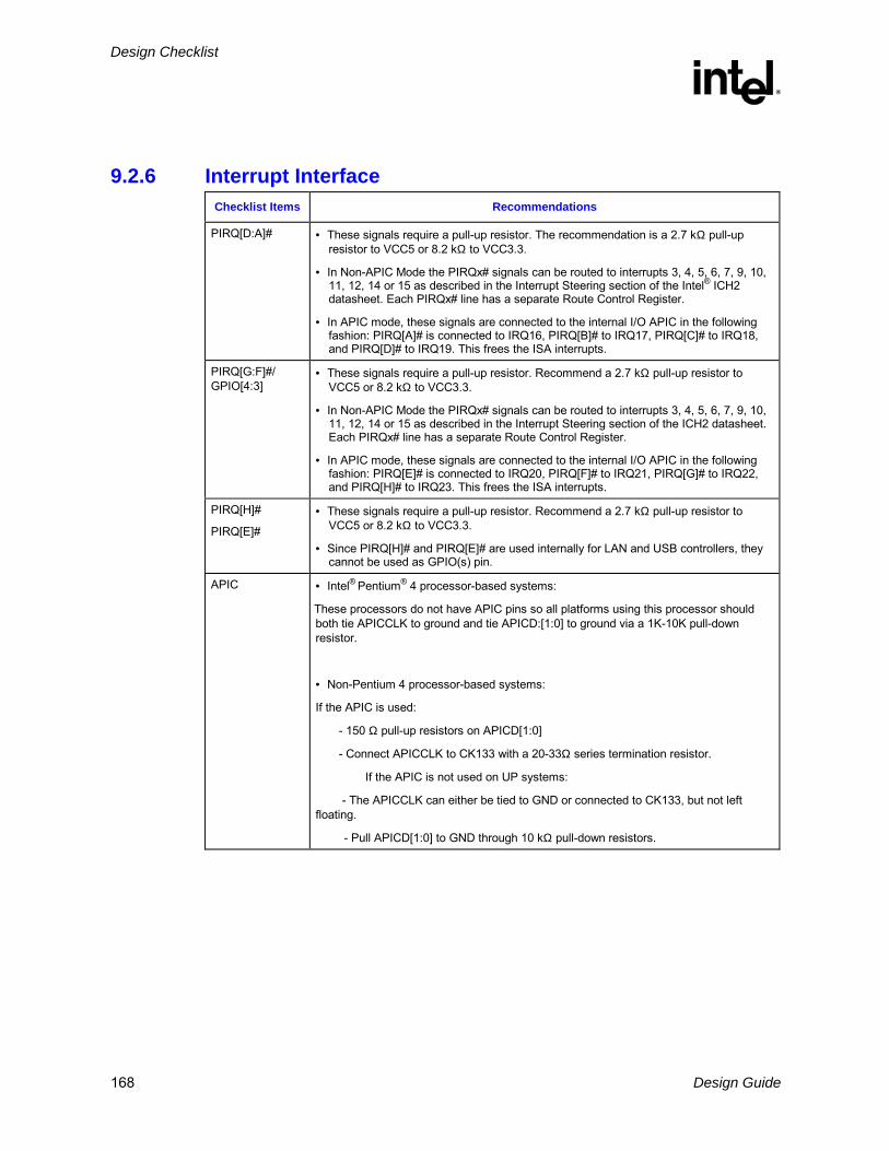
Design Checklist
R
168 Design Guide
9.2.6 Interrupt Interface Checklist Items Recommendations
PIRQ[D:A]# • These signals require a pull-up resistor. The recommendation is a 2.7 kΩ pull-up resistor to VCC5 or 8.2 kΩ to VCC3.3.
• In Non-APIC Mode the PIRQx# signals can be routed to interrupts 3, 4, 5, 6, 7, 9, 10, 11, 12, 14 or 15 as described in the Interrupt Steering section of the Intel® ICH2 datasheet. Each PIRQx# line has a separate Route Control Register.
• In APIC mode, these signals are connected to the internal I/O APIC in the following fashion: PIRQ[A]# is connected to IRQ16, PIRQ[B]# to IRQ17, PIRQ[C]# to IRQ18, and PIRQ[D]# to IRQ19. This frees the ISA interrupts.
PIRQ[G:F]#/ GPIO[4:3]
• These signals require a pull-up resistor. Recommend a 2.7 kΩ pull-up resistor to VCC5 or 8.2 kΩ to VCC3.3.
• In Non-APIC Mode the PIRQx# signals can be routed to interrupts 3, 4, 5, 6, 7, 9, 10, 11, 12, 14 or 15 as described in the Interrupt Steering section of the ICH2 datasheet. Each PIRQx# line has a separate Route Control Register.
• In APIC mode, these signals are connected to the internal I/O APIC in the following fashion: PIRQ[E]# is connected to IRQ20, PIRQ[F]# to IRQ21, PIRQ[G]# to IRQ22, and PIRQ[H]# to IRQ23. This frees the ISA interrupts.
PIRQ[H]#
PIRQ[E]#
• These signals require a pull-up resistor. Recommend a 2.7 kΩ pull-up resistor to VCC5 or 8.2 kΩ to VCC3.3.
• Since PIRQ[H]# and PIRQ[E]# are used internally for LAN and USB controllers, they cannot be used as GPIO(s) pin.
APIC • Intel® Pentium® 4 processor-based systems:
These processors do not have APIC pins so all platforms using this processor should both tie APICCLK to ground and tie APICD:[1:0] to ground via a 1K-10K pull-down resistor.
• Non-Pentium 4 processor-based systems:
If the APIC is used:
- 150 Ω pull-up resistors on APICD[1:0]
- Connect APICCLK to CK133 with a 20-33Ω series termination resistor.
If the APIC is not used on UP systems:
- The APICCLK can either be tied to GND or connected to CK133, but not left floating.
- Pull APICD[1:0] to GND through 10 kΩ pull-down resistors.

Design Checklist
R
Design Guide 169
9.2.7 GPIO Checklist Checklist Items Recommendations
All • Ensure ALL unconnected signals are OUTPUTS ONLY!
GPIO[7:0] • These pins are in the Main Power Well. Pull-ups must use the VCC3.3 plane. Unused core well inputs must either be pulled up to VCC3.3 or pulled down. Inputs must not be allowed to float. These signals are 5V tolerant.
• GPIO[1:0] can be used as REQ[A:B]#. GPIO[1] can also used as PCI REQ5#.
[13:11], GPIO[8] • These pins are in the Resume Power Well. Pull-ups must use the VCCSUS3.3 plane. These are the only GPI signals in the resume well with associated status bits in the GPE1_STS register. Unused resume well inputs must be pulled up to VCCSUS3.3. These signals are not 5V tolerant.
• These are the only GPIs that can be used as ACPI compliant wake events.
GPIO[23:16] • Fixed as output only. Can be left NC. In Main Power Well. GPIO22 is open drain.
GPIO[24,25,27,28] • These I/O pins can be NC. These pins are in the resume power well.
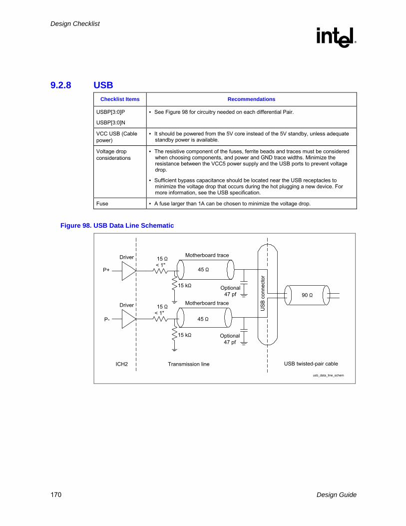
Design Checklist
R
170 Design Guide
9.2.8 USB Checklist Items Recommendations
USBP[3:0]P
USBP[3:0]N
• See Figure 98 for circuitry needed on each differential Pair.
VCC USB (Cable power)
• It should be powered from the 5V core instead of the 5V standby, unless adequate standby power is available.
Voltage drop considerations
• The resistive component of the fuses, ferrite beads and traces must be considered when choosing components, and power and GND trace widths. Minimize the resistance between the VCC5 power supply and the USB ports to prevent voltage drop.
• Sufficient bypass capacitance should be located near the USB receptacles to minimize the voltage drop that occurs during the hot plugging a new device. For more information, see the USB specification.
Fuse • A fuse larger than 1A can be chosen to minimize the voltage drop.
Figure 98. USB Data Line Schematic
15 kΩ
15 kΩ
15 Ω
15 Ω
ICH2
P+
P-
< 1"
< 1"
45 Ω
45 Ω
Driver
Driver
Transmission line
Motherboard trace
Motherboard trace
usb_data_line_schem
USB
con
nect
or
90 Ω
USB twisted-pair cable
Optional47 pf
Optional47 pf

Design Checklist
R
Design Guide 171
9.2.9 Power Management Checklist Items Recommendations
THRM# Connect to temperature Sensor. Pull-up if not used.
SLP_S3#
SLP_S5#
• No pull-up/down resistors needed. Signals driven by Intel® ICH2.
PWROK • This signal should be connected to power monitoring logic, and should go high no sooner than 10 ms after both VCC3.3 and VCC1.8 have reached their nominal voltages
PWRBTN# • No extra pull-up resistors. These signals have integrated pull-ups of 24 kΩ.
RI# • RI# does not have an internal pull-up. Recommend an 8.2 kΩ pull-up resistor to Resume well.
• If this signal is enabled as a wake event, it is important to keep this signal powered during the power loss event. If this signal goes low (active), when power returns, the RI_STS bit will be set and the system will interpret that as a wake event.
RSMRST# • This signal should be connected to power monitoring logic, and should go high no sooner than 10 ms after both VCCSus3_3 and VCCSus1_8 have reached their nominal voltages. Can be tied to RSMPWROK on Desktop Platforms.
9.2.10 Processor Signals Checklist Items Recommendations
A20M#, CPUSLP#, IGNNE#, INIT#, INTR, NMI, SMI#, STPCLK#
• Internal circuitry has been added to the Intel® ICH2, external pull-up resistors are not needed.
FERR# • Requires Weak external pull-up resistor to VCCCMOS.
RCIN#
A20GATE
• Pull-up signals to VCC3.3 through a 10 kΩ resistor.
CPUPWRGD • Connect to the processors CPUPWRGD input. Requires weak external pull-up resistor.

Design Checklist
R
172 Design Guide
9.2.11 System Management Checklist Items Recommendations
SMBDATA
SMBCLK
• Requires external pull-up resistors. See Section 6.17 to determine the appropriate power well to use to tie the pull-up resistors. (Core well, suspend well, or a combination.)
• Value of pull-up resistors determined by line load. Typical value used is 8.2 kΩ.
SMBALERT#/ GPIO[11]
• See GPIO section if SMBALERT# not implemented
SMLINK[1:0] • Requires external pull-up resistors. See Section 6.17 to determine the appropriate power well to use to tie the pull-up resistors. (Core well, suspend well, or a combination.)
• Value of pull-up resistors determined by line load. Typical value used is 8.2 kΩ.
INTRUDER# • Pull signal to VCCRTC (VBAT), if not needed.
9.2.12 ISA Bridge Checklist Checklist Items Recommendations
Intel® ICH2 GPO[21] / MISA NOGO input
• Connect ICH2 GPO[21] to MISA NOGO input.
• If GPO[21] is not available on the ICH2, any other GPO that defaults High in the system can be used. GPO[21] is the only ICH2 GPO that defaults high.
ICH2 AD22 / MISA IDSEL input
• Connect ICH2 AD22 to the MISA IDSEL input.
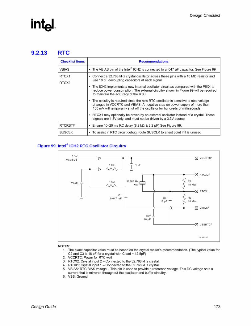
Design Checklist
R
Design Guide 173
9.2.13 RTC Checklist Items Recommendations
VBIAS • The VBIAS pin of the Intel® ICH2 is connected to a .047 µF capacitor. See Figure 99
RTCX1
RTCX2
• Connect a 32.768 kHz crystal oscillator across these pins with a 10 MΩ resistor and use 18 pF decoupling capacitors at each signal.
• The ICH2 implements a new internal oscillator circuit as compared with the PIIX4 to reduce power consumption. The external circuitry shown in Figure 99 will be required to maintain the accuracy of the RTC.
• The circuitry is required since the new RTC oscillator is sensitive to step voltage changes in VCCRTC and VBIAS. A negative step on power supply of more than 100 mV will temporarily shut off the oscillator for hundreds of milliseconds.
• RTCX1 may optionally be driven by an external oscillator instead of a crystal. These signals are 1.8V only, and must not be driven by a 3.3V source.
RTCRST# • Ensure 1020 ms RC delay (8.2 kΩ & 2.2 µF) See Figure 99.
SUSCLK • To assist in RTC circuit debug, route SUSCLK to a test point if it is unused
Figure 99. Intel® ICH2 RTC Oscillator Circuitry
C31
18 pF
3.3VVCCSUS
1 kΩ
Vbatt 1 kΩ
C10.047 uF
32768 HzXtal
R110 MΩ
R210 MΩ
C21
18 pF
1 µF
VCCRTC2
RTCX23
RTCX14
VBIAS5
VSSRTC6
rtc_cir.vsd
NOTES: 1. The exact capacitor value must be based on the crystal makers recommendation. (The typical value for
C2 and C3 is 18 pF for a crystal with Cload = 12.5pF) 2. VCCRTC: Power for RTC well 3. RTCX2: Crystal input 2 Connected to the 32.768 kHz crystal. 4. RTCX1: Crystal input 1 Connected to the 32.768 kHz crystal. 5. VBIAS: RTC BIAS voltage This pin is used to provide a reference voltage. This DC voltage sets a
current that is mirrored throughout the oscillator and buffer circuitry. 6. VSS: Ground
Design Checklist
R
174 Design Guide
9.2.14 AC’97 Checklist Items Recommendations
AC_BITCLK • No extra pull-down resistors required.
• When nothing is connected to the link, BIOS must set a shut off bit for the internal keeper resistors to be enabled. At that point, you do not need pull-ups/pull-downs on any of the link signals.
AC_SYNC • No extra pull-down resistors required. Some implementations add termination for signal integrity. Platform specific.
AC_SDOUT • Requires a jumper to 8.2 kΩ pull-up resistor. Should not be stuffed for default operation.
• This pin has a weak internal pull-down. To properly detect a safe_mode condition a strong pull-up will be required to over-ride this internal pull-down.
AC_SDIN[1], AC_SDIN[0]
• Requires pads for weak 10 kΩ pull-downs. Stuff resistor for unused AC_SDIN signal or AC_SDIN signal going to the CNR connector.
• AC_SDIN[1:0] are inputs to an internal OR gate. If a pin is left floating, the output of the OR gate will be erroneous.
• If there is no codec on the system board, then both AC_SDIN[1:0] should be pull-down externally with resisters to ground.
CDC_DN_ENAB# • If the primary codec is down on the motherboard, this signal must be low to indicate the motherboard codec is active and controlling the AC 97 interface.
• ZO AC97 = 60 Ω + 15%
• 5 mil trace width, 5 mil spacing between traces
• Max Trace Length ICH2/Codec/CNR = 14 inches
9.2.15 Miscellaneous Signals Checklist Items Recommendations
SPKR • No extra pull-up resistors. Has integrated pull-up of between 18 kΩ and 42 kΩ. The integrated pull-up is only enabled at boot/reset for strapping functions; at all other times, the pull-up is disabled.
• A low effective impedance may cause the TCO Timer Reboot function to be erroneously disabled.
• Effective Impedance due speaker and codec circuitry must be greater than 50 kΩ or a means to isolate the resistive load from the signal while PWROK is low be found. See Figure 100.
TP[0] • Requires external pull-up resistor to VCCSUS3.3
FS[0] • Rout to a testpoint. Intel® ICH2 contains an integrated pull-up for this signal. Testpoint used for manufacturing appears in XOR tree.

Design Checklist
R
Design Guide 175
Figure 100. SPKR Circuitry
Speaker_Circuit
Stuff jumper todisable time-outfeature.
R < 7.3 kΩReff > 50 kΩ
Effective Impedencedue to speaker andcodec circuit.
18 kΩ - 42 kΩ
Integrated Pull-up
3.3V
ICH2

Design Checklist
R
176 Design Guide
9.2.16 Power Checklist Items Recommendations
V_CPU_IO[1:0] • The power pins should be connected to the proper power plane for the processor 's CMOS Compatibility Signals. Use one 0.1 µF decoupling capacitor.
VCCRTC • No clear CMOS jumper on VCCRTC. Use a jumper on RTCRST# or a GPI, or use a safemode strapping for Clear CMOS
VCC3.3 • Requires six 0.1 µF decoupling capacitors
VCCSus3.3 • Requires one 0.1 µF decoupling capacitor.
VCC1.8 • Requires two 0.1 µF decoupling capacitors.
VCCSus1.8 • Requires one 0.1 µF decoupling capacitor.
5VREF_SUS • Requires one 0.1 µF decoupling capacitor.
• V5REF_SUS only affects 5V-tolerance for USB OC:[3:0]# pins and can be connected to either VccSUS3_3 or 5V_Always/5V_AUX if 5V tolerance on these OC:[3:0]# is not needed. If 5V tolerance on OC:[3:0]# is needed then V5REF_SUS USB must be connected to 5V_Always/5V_AUX which remains powered during S5.
5VREF • 5VREF is the reference voltage for 5V tolerant inputs in the Intel® ICH2. Tie to pins VREF[2:1]. 5VREF must power up before or simultaneous to VCC3.3. It must power down after or simultaneous to VCC3.3. Refer to Figure 101 for an example circuit schematic that may be used to ensure the proper 5VREF sequencing.
Figure 101. V5REF Circuitry
Vcc Supply(3.3 V)
1 KΩ
5V Supply
1 µF
To System VREF To System
3.3V_5V_Seq_Ckt
Design Checklist
R
Design Guide 177
9.2.17 IDE Checklist Checklist Items Recommendations
PDD[15:0], SDD[15:0]
• No extra series termination resistors or other pull-ups/pull-downs are required. These signals have integrated series resistors.
NOTE: Simulation data indicates that the integrated series termination resistors can range from 31 Ω to 43 Ω.
• PDD7/SDD7 does not require a 10 kΩ pull-down resistor. Refer to ATA ATAPI-4 specification.
PDIOW#, PDIOR#, PDDACK#, PDA[2:0], PDCS1#, PDCS3#, SDIOW#, SDIOR#, SDDACK#, SDA[2:0], SDCS1#, SDCS3#
• No extra series termination resistors. Pads for series resistors can be implemented should the system designer have signal integrity concerns. These signals have integrated series resistors.
NOTE: Simulation data indicates that the integrated series termination resistors can range from 31 Ω to 43 Ω.
PDREQ
SDREQ
• No extra series termination resistors. No pull-down resistors needed.
• These signals have integrated series resistors in the Intel® ICH2. These signals have integrated pull-down resistors in the ICH2.
PIORDY
SIORDY
• No extra series termination resistors. These signals have integrated series resistors in the ICH2. Pull-up to VCC3.3 via a 4.7 kΩ resistor.
IRQ14, IRQ15 • Recommend 8.2 kΩ10 kΩ pull-up resistors to VCC3.3.
• No extra series termination resistors.
IDERST# • The PCIRST# signal should be buffered to form the IDERST# signal. A 33 Ω series termination resistor is recommended on this signal.
Cable Detect: • Host Side/Device Side Detection: Connect IDE pin PDIAG/CBLID to an Intel® ICH2 GPIO pin. Connect a 10 kΩ resistor to GND on the signal line. The 10 kΩ resistor to GND prevents GPI from floating if no devices are present on either IDE interface. Allows use of 3.3V and 5V tolerant GPIOs.
• Device Side Detection: Connect a 0.047 µF capacitor from IDE pin PDIAG/CBLID to GND. No ICH2 connection.
NOTE: All ATA66/ATA100 drives will have the capability to detect cables
NOTE: The maximum trace length from the ICH2 to the ATA connector is 8 inches.

Design Checklist
R
178 Design Guide
Figure 102. Host/Device Side Detection Circuitry
80-conductorIDE cable
IDE drive
5 V
ICH2
GPIO
GPIO
Open
IDE drive
5 V
40-conductorcable
IDE drive
5 V
PDIAG#ICH2
GPIO
GPIO
IDE drive
5 V
PDIAG#
PDIAG#PDIAG#
10 kΩ
10 kΩ
To secondaryIDE connector
To secondaryIDE connector
PDIAG#/CBLID#
PDIAG#/CBLID#
10 kΩ
10 kΩ
10 kΩ
10 kΩ
IDE_combo_cable_det
Figure 103. Device Side Only Cable Detection
80-conductorIDE cable
IDE drive
5 V
ICH2
Open
IDE drive
5 V
40-conductorcable
IDE drive
5 V
PDIAG#ICH2
IDE drive
5 V
PDIAG#
PDIAG#PDIAG#PDIAG#/CBLID#
PDIAG#/CBLID#
10 kΩ
10 kΩ
10 kΩ
10 kΩ
IDE_dev_cable_det
0.047 µF
0.047 µF
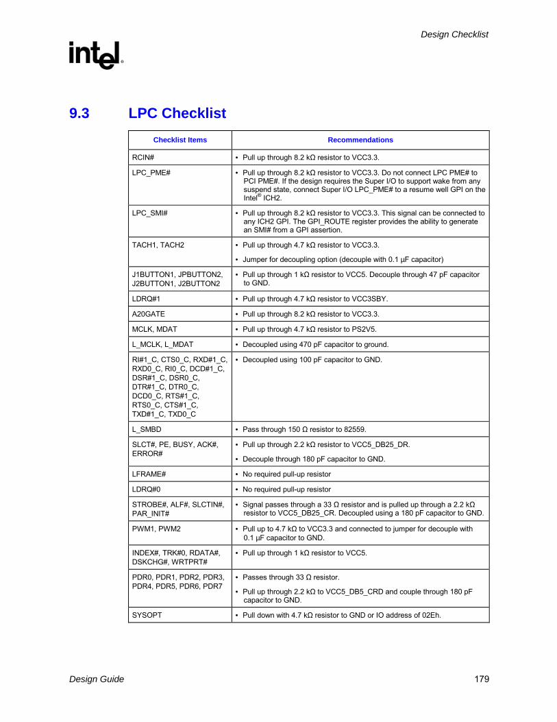
Design Checklist
R
Design Guide 179
9.3 LPC Checklist
Checklist Items Recommendations
RCIN# • Pull up through 8.2 kΩ resistor to VCC3.3.
LPC_PME# • Pull up through 8.2 kΩ resistor to VCC3.3. Do not connect LPC PME# to PCI PME#. If the design requires the Super I/O to support wake from any suspend state, connect Super I/O LPC_PME# to a resume well GPI on the Intel® ICH2.
LPC_SMI# • Pull up through 8.2 kΩ resistor to VCC3.3. This signal can be connected to any ICH2 GPI. The GPI_ROUTE register provides the ability to generate an SMI# from a GPI assertion.
TACH1, TACH2 • Pull up through 4.7 kΩ resistor to VCC3.3.
• Jumper for decoupling option (decouple with 0.1 µF capacitor)
J1BUTTON1, JPBUTTON2, J2BUTTON1, J2BUTTON2
• Pull up through 1 kΩ resistor to VCC5. Decouple through 47 pF capacitor to GND.
LDRQ#1 • Pull up through 4.7 kΩ resistor to VCC3SBY.
A20GATE • Pull up through 8.2 kΩ resistor to VCC3.3.
MCLK, MDAT • Pull up through 4.7 kΩ resistor to PS2V5.
L_MCLK, L_MDAT • Decoupled using 470 pF capacitor to ground.
RI#1_C, CTS0_C, RXD#1_C, RXD0_C, RI0_C, DCD#1_C, DSR#1_C, DSR0_C, DTR#1_C, DTR0_C, DCD0_C, RTS#1_C, RTS0_C, CTS#1_C, TXD#1_C, TXD0_C
• Decoupled using 100 pF capacitor to GND.
L_SMBD • Pass through 150 Ω resistor to 82559.
SLCT#, PE, BUSY, ACK#, ERROR#
• Pull up through 2.2 kΩ resistor to VCC5_DB25_DR.
• Decouple through 180 pF capacitor to GND.
LFRAME# • No required pull-up resistor
LDRQ#0 • No required pull-up resistor
STROBE#, ALF#, SLCTIN#, PAR_INIT#
• Signal passes through a 33 Ω resistor and is pulled up through a 2.2 kΩ resistor to VCC5_DB25_CR. Decoupled using a 180 pF capacitor to GND.
PWM1, PWM2 • Pull up to 4.7 kΩ to VCC3.3 and connected to jumper for decouple with 0.1 µF capacitor to GND.
INDEX#, TRK#0, RDATA#, DSKCHG#, WRTPRT#
• Pull up through 1 kΩ resistor to VCC5.
PDR0, PDR1, PDR2, PDR3, PDR4, PDR5, PDR6, PDR7
• Passes through 33 Ω resistor.
• Pull up through 2.2 kΩ to VCC5_DB5_CRD and couple through 180 pF capacitor to GND.
SYSOPT • Pull down with 4.7 kΩ resistor to GND or IO address of 02Eh.

Design Checklist
R
180 Design Guide
9.4 System Checklist Checklist Items Recommendations
KEYLOCK# • Pull up through 10 kΩ resistor to VCC3.3.
PBTN_IN • Connects to PBSwitch and PBin.
PWRLED • Pull up through a 220 Ω resistor to VCC5.
R_IRTX • Signal IRTX after it is pulled down through 4.7 kΩ resistor to GND and passes through 82 Ω resistor.
IRRX • Pull up to 100 kΩ resistor to VCC3.3.
• When signal is input for SI/O decouple through 470 pF capacitor to GND
IRTX • Pull down through 4.7 kΩ to GND.
• Signal passes through 82 Ω resistor.
• When signal is input to SI/O decouple through 470 pF capacitor to GND
FP_PD • Decouple through a 470 pF capacitor to GND.
• Pull up 470 Ω to VCC5.
PWM1, PWM2 • Pull up through a 4.7 kΩ resistor to VCC3.3.
9.5 FWH Checklist Checklist Items Recommendations
No floating inputs • Unused FGPI pins must be tied to a valid logic level.
WPROT, TBLK_LCK • Pull up through a 4.7 kΩ resistor to VCC3.3.
R_VPP • Pulled up to VCC3.3 and decoupled with two 0.1 µF capacitors to GND.
FGPI0_PD, FGPI1_PD, FGPI2_PD, FPGI3_PD, FPGI4_PD, IC_PD
• Pull down through a 8.2 kΩ resistor to GND.
FWH_ID1, FWH_ID2, FWH_ID3 • Pull down to GND.
INIT# • FWH INIT# must be connected to processor INIT#.
RST# • FWH RST# must be connected to PCIRST#.
ID[3:0] • For a system with only one FWH device, tie ID[3:0] to ground.

Design Checklist
R
Design Guide 181
9.6 Clock Synthesizer Checklist Checklist Items Recommendations
REFCLK • Connects to R-RefCLK, USB_CLK, SIO_CLK14, and ICHCLK14.
ICH_3V66/3V66_0, DOTCLK • Passes through 33 Ω resistor.
• When signal is input for Intel® ICH2, it is pulled down through a 18 pF capacitor to GND.
DCLK/DCLK_WR • Passes through 33 Ω resistor.
• When signal is input for GMCH, it is pulled down through a 22 pF capacitor to GND.
CPUHCLK/CPU_0_1 • Passes through 33 Ω resistor.
• When signal is input for 370PGA, decouple through a 18 pF capacitor to GND.
R_REFCLK • REFCLK passed through 10 kΩ resistor.
• When signal is input for 370PGA, pull up through 1 kΩ resistor to VCC3.3 and pass through 10 kΩ resistor.
USB_CLK, ICH_CLK14 • REFCLK passed through 10 Ω resistor.
XTAL_IN, XTAL_OUT • Passes through 14.318 MHz oscillator.
• Pulled down through 18 pF capacitor to GND.
SEL1_PU • Pulled up via MEMV3 circuitry through 8.2 kΩ resistor.
FREQSEL • Connected to clock frequency selection circuitry through 10 kΩ resistor.
L_VCC2_5 • Connects to VDD2_5[01] through ferrite bead to VCC2.5.
GMCHHCLK/CPU_1, ITPCLK/CPU_2, PCI_0/PCLK_OICH, PCI_1/PCLK_1, PCI_2/PCLK_2, PCI_3/PCLK_3, PCI_4/PCLK_4, PCI_5/PCLK_5, PCI_6/PCLK_6, APICCLK_CPU/APIC_0, APICCLK)ICH/APIC_1, USBCLK/USB_0, GMCH_3V66/3V66_1, AGPCLK_CONN
• Passes through 33 Ω resistor.
MEMCLK0/DRAM_0, MEMCLK1/DRAM_1, MEMCLK2/DRAM_2, MEMCLK3/DRAM_3, MEMCLK4/DRAM_4, MEMCLK5/DRAM_5, MEMCLK6/DRAM_6, MEMCLK7/DRAM_7, SCLK
• Pass through 22 Ω resistor.
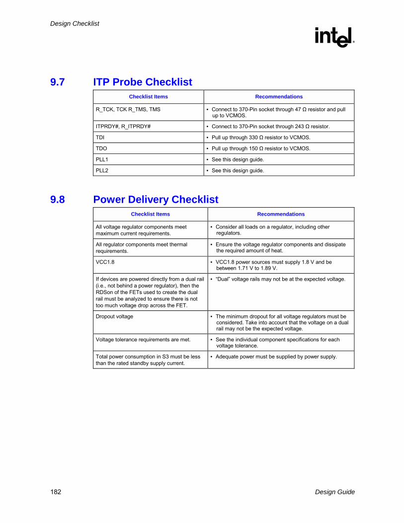
Design Checklist
R
182 Design Guide
9.7 ITP Probe Checklist Checklist Items Recommendations
R_TCK, TCK R_TMS, TMS • Connect to 370-Pin socket through 47 Ω resistor and pull up to VCMOS.
ITPRDY#, R_ITPRDY# • Connect to 370-Pin socket through 243 Ω resistor.
TDI • Pull up through 330 Ω resistor to VCMOS.
TDO • Pull up through 150 Ω resistor to VCMOS.
PLL1 • See this design guide.
PLL2 • See this design guide.
9.8 Power Delivery Checklist Checklist Items Recommendations
All voltage regulator components meet maximum current requirements.
• Consider all loads on a regulator, including other regulators.
All regulator components meet thermal requirements.
• Ensure the voltage regulator components and dissipate the required amount of heat.
VCC1.8 • VCC1.8 power sources must supply 1.8 V and be between 1.71 V to 1.89 V.
If devices are powered directly from a dual rail (i.e., not behind a power regulator), then the RDSon of the FETs used to create the dual rail must be analyzed to ensure there is not too much voltage drop across the FET.
• Dual voltage rails may not be at the expected voltage.
Dropout voltage • The minimum dropout for all voltage regulators must be considered. Take into account that the voltage on a dual rail may not be the expected voltage.
Voltage tolerance requirements are met. • See the individual component specifications for each voltage tolerance.
Total power consumption in S3 must be less than the rated standby supply current.
• Adequate power must be supplied by power supply.

Third-Party Vendor Information
R
Design Guide 183
10 Third-Party Vendor Information This design guide has been compiled to give an overview of important design considerations while providing sources for additional information. This chapter includes information regarding various third-party vendors who provide products to support the 810ET2 chipset. The list of vendors can be used as a starting point for the designer. Intel does not endorse any one vendor, nor guarantee the availability or functionality of outside components. Contact the manufacturer for specific information regarding performance, availability, pricing and compatibility.
Table 51. Super I/O
Vendors Contact Phone
SMC Dave Jenoff (909) 244-4937
National Robert Reneau (408) 721-2981
ITE Don Gardenhire (512)388-7880
Winbond James Chen (02) 27190505 - Taipei office
Table 52. Clock Generation
Vendors Contact Phone
Cypress John Wunner 206-821-9202 x325
ICS Raju Shah 408-925-9493
IC Works Jeff Keip 408-922-0202, x1185
IMI Elie Ayache 408-263-6300, x235
PERICOM Ken Buntaran 408-435-1000
Table 53. Memory Vendors
http://developer.intel.com/design/motherbd/se/se_mem.htm
Table 54. Voltage Regulator Vendors
Vendors Contact Phone
Linear Tech Corp. Stuart Washino 408-432-6326
Celestica Dariusz Basarab 416-448-5841
Corsair Microsystems John Beekley 888-222-4346
Delta Electronics Colin Weng 886-2-6988, x233(Taiwan)
N. America: Delta Products Corp.
Maurice Lee 510-770-0660, x111
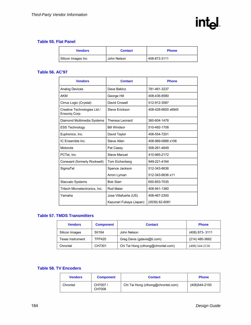
Third-Party Vendor Information
R
184 Design Guide
Table 55. Flat Panel
Vendors Contact Phone
Silicon Images Inc John Nelson 408-873-3111
Table 56. AC’97
Vendors Contact Phone
Analog Devices Dave Babicz 781-461-3237
AKM George Hill 408-436-8580
Cirrus Logic (Crystal) David Crowell 512-912-3587
Creative Technologies Ltd./ Ensoniq Corp.
Steve Erickson 408-428-6600 x6945
Diamond Multimedia Systems Theresa Leonard 360-604-1478
ESS Technology Bill Windsor 510-492-1708
Euphonics, Inc. David Taylor 408-554-7201
IC Ensemble Inc. Steve Allen 408-969-0888 x106
Motorola Pat Casey 508-261-4649
PCTel, Inc. Steve Manuel 410-965-2172
Conexant (formerly Rockwell) Tom Eichenberg 949-221-4164
SigmaTel Spence Jackson
Arron Lyman
512-343-6636
512-343-6636 x11
Staccato Systems Bob Starr 650-853-7035
Tritech Microelectronics, Inc. Rod Maier 408-941-1360
Yamaha Jose Villafuerte (US)
Kazunari Fukaya (Japan)
408-467-2300
(0539) 62-6081
Table 57. TMDS Transmitters
Vendors Component Contact Phone
Silicon Images SII164 John Nelson (408) 873- 3111
Texas Instrument TFP420 Greg Davis ([email protected]) (214) 480-3662
Chrontel CH7301 Chi Tai Hong ([email protected]) (408) 544-2150
Table 58. TV Encoders
Vendors Component Contact Phone
Chrontel CH7007 / CH7008
Chi Tai Hong ([email protected]) (408)544-2150

Third-Party Vendor Information
R
Design Guide 185
Vendors Component Contact Phone
Chrontel CH7010 / CH7011
Chi Tai Hong ([email protected]) (408)544-2150
Conexant CN870 / CN871 Eileen Carlson ([email protected])
(858) 713-3203
Focus FS450 / FS451 Bill Schillhammer ([email protected])
(978) 661-0146
Philips SAA7102A Marcus Rosin ([email protected])
None
Texas Instrument TFP6022/ TFP6024
Greg Davis ([email protected])
(214) 480-3662
Table 59. Combo TMDS Transmitters/TV Encoders
Vendors Component Contact Phone
Chrontel CH7009/
CH7010
Chi Tai Hong ([email protected]) (408) 544-2150
Texas Instrument TFP6422/ TFP6424
Greg Davis ([email protected])
(214) 480-3662
Table 60. LVDS Transmitter
Vendors Component Contact Phone
National Semiconductor
387R Jason Lu ([email protected])
(408) 721-7540
A
A
A A
INTEL® PENTIUM® III & INTEL® CELERON (R)PROCESSOR/ 810E2 CHIPSET UNIVERSALSOCKET 370 PLATFORM
UNIPROCESSOR CUSTOMER REFERENCE SCHEMATICS
REVISION 1.0
Title PageCover Sheet
Block Diagram370-pin socke t
82810eDisplay Cache
System Memory
ICH2FWH & UDAM 100 IDE1-2
Super I/OPCI Connectors
USB Connectors
AC97 CODECAudio I /O
Kybrd / Mse / F. Disk / Gme ConnectorsDigi tal Video Out
Video ConnectorsFront Panel & CNR
ATX Power & H/W M onitorVoltage Regulators
System Configuration
1
23 , 4
7, 8, 910
11, 12
13, 1415
1617, 18
19
2021
22
2324
25
31
32
** Please note these schematics are subject to change.
THESE SCHEMATICS ARE PROVIDED "AS IS" WITH NO WARRANTIESWHATSOEVER, INCLUDING ANY WARRANTY OF MERCHANTABILITY, FITNESSFOR ANY PARTICULAR PURPOSE, OR ANY WARRANTY OTHERWISE ARISINGOUT OF PROPOSAL, SPECIFICATION OR SAMPLES.
Information in this document is provided in connection w ith Intel products. No license,express or implied, by estoppel or otherwise, to any intellectual property rights isgranted by this document. Except as provided in Intel 's Terms and Conditions of Salefor such products, Intel assumes no liability whatsoever, and Intel disclaims anyexpress or implied warranty, relating to sale and/or use of Intel products includingliability or warranties relating to fitness for a particu lar purpose, merchantability, orinfringement of any patent, copyright or other intellectual property right. Intel productsare not intended for use in medical, l i fe saving o r life sustaining applications.
Intel may make changes to specifications and product descriptions at any time,without notice.
The Intel® Celeron(R) processor and Intel® 810e2 chipset may contain design defectsor errors known as errata which may cause the product to deviate from publishedspecifications. Current characterized errata are available on request.
Copyright (c) Intel Corpora tion 2001.
* Third-party brands and names are the property of thei r respective owners.
5AGTL TerminationClock Synthesi zer 6
WOL, WOR & 2S1P
26
35, 36
Pullup Resistors
UMB CircuitsUnused Gates & Decoupling capacitors
27, 28
29, 30
33, 34
Intel® 810e2 Chipset Universal Socke t 370 CRBCover Sheet
36
1.0
9/02/01
1
IAMG Platform Apps Engineering1900 Prairie City RoadFolsom, Ca. 95630
REV.
Last Revision Date:
Sheet:of
Title:
intel

A
A
A A
DA
TA
CTR
L
AD
DR
Term
VRM
ICH2
KeyboardMouse
Floppy ParallelSerial 1
SIO
Clock
PC
I CO
NN
1
PC
I CO
NN
2
PC
I CO
NN
3
Block Diagram
2 DIMMModules
USB Port 1-4
CNRCONNECTOR
CTR
L
DA
TA
AD
DR
IDE Primary
IDE SecondaryUltraDMA/100
PCI CNTRL
PCI ADDR/DATA
AC'97 Link
FirmWare Hub
LP
C B
us
GMCH
Game Port
Display CacheMemory
Out DeviceDigital Video
370-PIN SOCKET PROCESSOR
GTL BUS
USB
AUDIOCODEC
Serial 2
Intel® 810e2 Chipset Universal Socke t 370 CRB
Block Diagram
36
1.0
9/02/012
IAMG Platform Apps Engineering1900 Prairie City RoadFolsom, Ca. 95630
REV.
Last Revision Date:
Sheet:of
Title:
intel

A
A
A A370 - Pin Socket Part 1
Intel® 810e2 Chipset Universal Socket 370 CRB
HREQ#0HREQ#1HREQ#2HREQ#3HREQ#4
HD#63
370-PIN SOCKET PART 1
36
1.0
9/02/01
3
IAMG Platform Apps Engineering1900 Prairie City RoadFolsom, Ca. 95630
REV.
R
Last Revision Date:
Sheet:of
Title:
intel
HA#[31:3]
HD#[63:0]
HA#16
HD#11
HD#2
HA#12HA#11
HA#3
HD#53
HD#34
HD#29
HA#30
HA#13
HA#9
HD#28
HD#17
HA#15
HD#61
HD#57
HD#26
HD#10
HD#3
HD#59
HD#20
HD#15
HD#13
HD#6
HD#0
HA#26
HA#19
HD#42
HD#25
HD#16
HD#14
HD#9HD#8HD#7
HA#6HA#5
HD#55
HD#47HD#46
HD#5
HA#25
HA#18
HA#14
HA#4
HD#52
HD#45
HD#23
HD#4
HA#28
HD#32HD#31
HD#44
HD#35
HD#33
HD#18
HA#17
HD#50
HD#43
HD#36
HD#22HD#21
HA#31
HA#27
HA#22
HD#58
HD#54
HD#49HD#48
HD#40
HD#1
HA#23
HA#10
HD#56
HD#12
HA#20
HD#30
HA#21
HA#8HA#7
HD#62
HD#51
HD#41
HD#38
HD#24
HA#24
HD#60
HD#39
HD#27HA#29
HD#37
HD#19
HA#[31:3] 5,7
HD#[63:0] 5,7
VID1 16,29
RS#[2:0]7
HREQ#[4:0] 5,7
VID2 16,29VID3 16,29
VID0 16,29
33 TUALDETVTTPWRGD 33
VID4 16,29
VCCVID
VTT
VTT
VTTR340
1K
U1A
Socket 370_9
W1T 4N1M6U1S3T 6J1S1P6Q3M4Q1L1N3U3H4R4P4H6L3G1F8G3K6E3E1
F12A5A3J3C5F6C1C7B2C9A9D8
D10C15D14D12
A7A11C11A21A15A17C13C25A13D16A23C21C19C27A19C23C17A25A27E25F16
AH26AH22AK28
AM
34A
H2
AD
2Z2 V
2M
2D
18H
2D
2A
L3A
K4
AG
5A
C5
Y5
U5
Q5
L5 G5
D4
B4
AM
6A
J7E
7B
8A
M10
AJ1
1E
11B
12A
M14
AJ1
5E
15B
16A
M18
AJ1
9E
19F
20B
20A
M22
AJ2
3D
22F
24B
24A
M26
AJ2
7D
26F
28B
28A
M30
D30
AF
32A
B32
X32
T32
P32
F32
B32
AH
34A
D34
Z34
V34
R34
M34
H34
D34
AK36
AF
36X
36T
36P
36K
36F
36A
37A
C33
AJ3
AL1
AN
3Y
37
AK8AH12AH8AN9AL15AH10AL9AH6AK10AN5AL7AK14AL5AN7AE1Z6AG3AC3AJ1AE3AB6AB4AF6Y3AA1AK6Z4AA3AD4X6AC1W3AF4
AL35AM36AL37AJ37
AK18AH16AH18AL19AL17C33C31A33A31E31C29E29A29
AH20AK16AL21AN11AN15G35AL13U37U35S37S33E23AN21AA35AA33
B26
C3
AK
2A
F2
AB
2T2 P
2K
2F4 E
5A
M4
AE
5A
A5
W5
S5
N5
J5 F2 D6
B6
AM
8A
J9E
9B
10A
M12
AJ1
3E
13B
14A
M16
AJ5
AJ1
7E
17B
18A
M20
AJ2
1D
20F
22A
M24
AJ2
5D
24F
26A
M28
AJ2
9D
28A
K34
F30
B30
AM
32A
H32
Z32
V32
R32
M32
H32
AF
34A
B34
X34
T34
P34
K34
F34
B34
AH
36B
22V
36R
36H
36D
36D
32A
D32
AH
24F
14K
32A
A37
Y35
HD#0HD#1HD#2HD#3HD#4HD#5HD#6HD#7HD#8HD#9HD#10HD#11HD#12HD#13HD#14HD#15HD#16HD#17HD#18HD#19HD#20HD#21HD#22HD#23HD#24HD#25HD#26HD#27HD#28HD#29HD#30HD#31HD#32HD#33HD#34HD#35HD#36HD#37HD#38HD#39HD#40HD#41HD#42HD#43HD#44HD#45HD#46HD#47HD#48HD#49HD#50HD#51HD#52HD#53HD#54HD#55HD#56HD#57HD#58HD#59HD#60HD#61HD#62HD#63
RS#0RS#1RS#2 G
ND
GN
DG
ND
GN
DG
ND
GN
DG
ND
GN
DG
ND
GN
DV
TTP
WR
GD
GN
DG
ND
GN
DG
ND
GN
DG
ND
GN
DG
ND
GN
DG
ND
GN
DG
ND
GN
DG
ND
GN
DG
ND
GN
DG
ND
GN
DG
ND
GN
DG
ND
GN
DG
ND
GN
DG
ND
GN
DG
ND
GN
DG
ND
GN
DG
ND
GN
DG
ND
GN
DG
ND
GN
DG
ND
GN
DG
ND
GN
DG
ND
GN
DG
ND
GN
DG
ND
GN
DG
ND
GN
DG
ND
GN
DG
ND
GN
D
GND/VID4
TU
ALD
ET
GN
DG
ND
GN
DG
ND
GN
DG
ND
GN
DR
SV
D-N
CG
ND
DY
N_O
EG
ND
HA#3HA#4HA#5HA#6HA#7HA#8HA#9
HA#10HA#11HA#12HA#13HA#14HA#15HA#16HA#17HA#18HA#19HA#20HA#21HA#22HA#23HA#24HA#25HA#26HA#27HA#28HA#29HA#30HA#31HA#32HA#33HA#34HA#35
VID0VID1VID2VID3
REQ#0REQ#1REQ#2REQ#3REQ#4DEP0#DEP1#DEP2#DEP3#DEP4#DEP5#DEP6#DEP7#
VTT1_5VTT1_5VTT1_5VTT1_5VTT1_5VTT1_5VTT1_5VTT1_5VTT1_5VTT1_5VTT1_5VTT1_5VTT1_5VTT1_5VTT1_5
VC
CV
IDV
CC
VID
VC
CV
IDV
CC
VID
VC
CV
IDV
CC
VID
VC
CV
IDV
CC
VID
VC
CV
IDV
CC
VID
VC
CV
IDV
CC
VID
VC
CV
IDV
CC
VID
VC
CV
IDV
CC
VID
VC
CV
IDV
CC
VID
VC
CV
IDV
CC
VID
VC
CV
IDV
CC
VID
VC
CV
IDV
CC
VID
VC
CV
IDV
CC
VID
VC
CV
IDV
CC
VID
VC
CV
IDV
CC
VID
VC
CV
IDV
CC
VID
VC
CV
IDV
CC
VID
VC
CV
IDV
CC
VID
VC
CV
IDV
CC
VID
VC
CV
IDV
CC
VID
VC
CV
IDV
CC
VID
VC
CV
IDV
CC
VID
VC
CV
IDV
CC
VID
VC
CV
IDV
CC
VID
VC
CV
IDV
CC
VID
VC
CV
IDV
CC
VID
VC
CV
IDV
CC
VID
VC
CV
IDV
CC
VID
VTT
VC
CV
IDV
CC
VID
VC
CV
IDV
CC
VID
VC
CV
IDV
CC
VID
VC
CV
IDV
CC
VID
VC
CV
IDV
CC
VID
VC
CV
IDV
CC
VID
VC
CV
IDV
CC
VID
VC
CV
IDV
CC
VID
VC
CV
IDV
CC
VID

1
1
A A
FSB66M100M
133Mrsvd
near VCMOS Processor PinVCMOS Decouping
370 - Pin Socket
Place 0603 Paclage
Part2
Place Site w/in 0.5"Do Not stuff Cof clock pin (W37)
GTLREF Generation CircuitUse 0603 Packages and distributewithin 500 mils of VREF pins
1
BSEL#00
0111
BSEL#1
00
CMOSREF
CMOSREF Generation
Circuit
No-stuff R199 page33
see page 34
see page 4
150
Intel® 810e2 Chipset Universal Socket 370 CRB370-Pin Socket Part 2
36
1.0
9/02/01
4
IAMG Platform Apps Engineering1900 Prairie City RoadFolsom, Ca. 95630
REV.
R
Last Revision Date:
Sheet:of
Title:
intel
GTLREFA
GTLREFA
A20M# 13
VTIN2 16,28
BPRI# 5,7
HITM# 5,7
BNR# 5,7
STPCLK# 13
INTR 13
HLOCK# 5,7
HTRDY# 5,7
IGNNE# 13
CPUSLP# 13
HIT# 5,7
DRDY# 5,7
BSEL#1 31
DEFER# 5,7
VCMOS 14
HADS# 7
BSEL#0 31
SMI# 13
DBSY# 5,7
APICD113,32APICD013,32
CPUHCLK6
CPURST#7
APICCLK_CPU6
CPU_PWGD13
ITPRDY#5
ITPCLK6
DBRESET#27
BR0# 5
GTLREF 7
CMOSREF
NMI 13
FERR# 13,32INIT# 13,15
THERMTRIP# 33THRMDN 16,28
33 TUAL5
ITPTCK33
VCC2_5
VTT
VTT
V3SBV3SB
VTT1_5
VTT1_5
VTT
VCC 2_5
VTT
VCCVID
VTT
C2
X18PF
BC3
0.1UF
R15
0
R340
1K
R9
330
U1B
Socket 370_9
X2
AG1
C37E21
AJ33AJ31
AN29
AL29AL31
AH28
S35
W33U33
E27
AN35AN37AN33AL33AK32
J37A35
G33E37C35E35
N33N35N37Q33Q35Q37
AK30
AM2F10
W35Y1R2
G37L33
J35L35J33
W37Y33
AK26AH4
X4
AB
36A
D36
Z36
E33
F18
K4
R6
V6
AD
6A
K12
AK
22
AH14AN17AN25AN19AK20AN27AL23AL25AL27AN31AE37
AE33AG35AH30AJ35M36L37AG33AC35AG37AE35
AC37AL11AN13AN23
B36AK24V4
RESVD21(BR1#)
EDGCTRL/VRSEL
CPUPRES#VCOREDET
BSEL0#BSEL1#
BR0#
THRMDNTHRMDP
THERMTRIP#
RTTCNTR
PLL1PLL2
SLEWCNTR
TDITDOTRST#TCKTMS
PREQ#PRDY#
BP2#BP3#BPM0#BPM1#
RSRVD6RSRVD7RSRVD8RSRVD9RSRVD10RSRVD11
RSRVD12/JBSEL1#
RSRVD13RSRVD15RSRVD16RSRVD17RSRVD18RSRVD19RSRVD20
PICD0PICD1PICCLKBCLKCLKREFPWRGOODRESET#RESET2#
V_C
MO
SV
1_5
V2_
5
VR
EF
0V
RE
F1
VR
EF
2V
RE
F3
VR
EF
4V
RE
F5
VR
EF
6V
RE
F7 BNR#
BPRI#TRDY#
DEFER#LOCK#DRDY#HITM#
HIT#DBSY#
ADS#FLUSH#
A20M#STPCLK#
SLP#SMI#
LINT0/INTRLINT1/NMI
INIT#FERR#
IGNNE#IERR#
RSP#AP0#AP1#
RP#
BINIT#AERR#BERR#
R1
1K
R339150,1%
R23 X0
R11
150
R275
22PR3
110,%1
MC1
4.7UF
R3461K
R6
1k
BC5
0.1UF
R12
150
R3
150
PR5
75,1%
R4
150
R317 0
R373330
R316 0
R14
1K
+C6 33uF (C size)
J1 HEADER 15X2
12345678910
1112131415161718192021222324252627282930
R33
90.9, 1%
R5
330
R1991.8K
PR4
110,%1
BC228
0.1UF
R319
243,1%
PR6
150,1%
R345 1k
R7
PR1
150,1%
BC6
0.1UF
R374
14
R33875.1%
C12
10PF
BC4
0.1UF
R10
680
R318243.1%
L2
4.7UH/SMD-0805
BC1
0.1UF
Q27FDN335N
PR2
150,1%
R8
150
BC2
0.1UF
R13
1K

5
5
4
4
3
3
2
2
1
1
D D
C C
B B
A A
AGTL Termination
" One Cap for each 2 R-Pack "
HEATSINK GROUNDING
Intel® 810e2 Chipset Universal Socket 370 CRBAGTL TERMINATION
36
1.0
9/02/01
5
IAMG Platform Apps Engineering1900 Prairie City RoadFolsom, Ca. 95630
REV.
R
Last Revision Date:
Sheet:of
Title:
intel
HA#23HA#17HA#22HA#31
HA#19HA#21HA#25HA#10
HA#13HA#16HA#3HA#9
HA#20HA#24HA#30
HA#28HA#15HA#12HA#5
HA#7
HA#11
HA#6HA#8
HA#4
HA#14
HA#27HA#29HA#26
HD#15HD#1HD#0HD#6
HD#4HD#9HD#5HD#8
HD#10HD#12
HD#24
HD#21
HD#17
HD#23
HD#16
HD#3
HD#20
HD#7
HD#18
HD#11
HD#30
HD#13
HD#14HD#2
HD#19
HD#29HD#31
HD#26HD#25
HD#35
HD#59HD#48HD#52HD#40
HD#60HD#62HD#61HD#56
HD#57HD#55
HD#46HD#58
HD#63
HD#53HD#50
HD#54
HD#45
HD#27
HD#51
HD#44
HD#42
HD#47HD#41HD#49
HD#22
HD#38
HD#39HD#37
HD#28HD#34
HD#36
HD#43HD#[63:0]
HA#[31:3]
HA#18
HD#32
HD#33
BNR# 4,7
HA#[31:3] 3,7
HD#[63:0] 3,7
HREQ#2 3,7HLOCK# 4,7
HITM# 4,7
HIT# 4,7
DRDY# 4,7
DBSY# 4,7
HREQ#4 3,7BPRI# 4,7HREQ#0 3,7
ITPRDY# 4
BR0# 4
HREQ#1 3,7
HTRDY# 4,7
DEFER# 4,7
HREQ#3 3,7
VTT1_5 VTT1_5 VTT1_5VTT1_5
VTT1_5
RN27
56/8P4R
1357
2468
R24 150
BC14
0.1UF
BC13
0.1UF
U1C
Socket 370_9
GD1GD2GD3GD4GD5GD6GD7GD8GD9
GD10GD11GD12GD13GD14GD15GD16GD17GD18
GD19GD20GD21GD22GD23GD24GD25GD26GD27
GD28GD29GD30GD31GD32GD33GD34GD35GD36
GNDGNDGNDGNDGNDGNDGNDGNDGND
GNDGNDGNDGNDGNDGNDGNDGNDGND
GNDGNDGNDGNDGNDGNDGNDGNDGND
GNDGNDGNDGNDGNDGNDGNDGNDGND
BC11
0.1UF
RN25
56/8P4R
1357
2468
BC18
0.1UF
BC17
0.1UF
RN21
56/8P4R
1357
2468
RN13
56/8P4R
1357
2468
RN16
56/8P4R
1357
2468
RN6
56/8P4R
1357
2468
RN2
56/8P4R
1357
2468
RN24
56/8P4R
1357
2468
RN8
56/8P4R
1357
2468
BC15
0.1UF
RN7
56/8P4R
1357
2468
MC3
4.7UF
RN15
56/8P4R
1357
2468
BC12
0.1UF
RN18
56/8P4R
1357
2468
RN1
56/8P4R
1357
2468
RN4
56/8P4R
1357
2468
RN19
56/8P4R
1357
2468
BC21
0.1UF
RN26
56/8P4R
1357
2468
BC16
0.1UF
BC7
0.1UF
RN14
56/8P4R
1357
2468
RN11
56/8P4R
1357
2468
RN20
56/8P4R
1357
2468
RN3
56/8P4R
1357
2468
RN23
56/8P4R
1357
2468
BC10
0.1UF
RN17
56/8P4R
1357
2468
RN5
56/8P4R
1357
2468
BC20
0.1UF
BC19
0.1UF
BC9
0.1UF
RN10
56/8P4R
1357
2468
BC8
0.1UF
RN28
56/8P4R
1357
2468
RN22
56/8P4R
1357
2468
RN9
56/8P4R
1357
2468
MC2
4.7UF
R25 10

A
A
A A
Clock Synthesizer
- Place all decoupling caps as close to VCC/GND pins as possibleNotes:
Minimize Stub Length from
CLK14 trace toJP20A.
- PCI_0/ICH pin has to go to the ICH.
- CPU_ITP pin must go to the ITP. It is the onlyCPU CLK that can be shut off through the SMBUS interface.
(This clock cannot be turned off through SMBus)
APIC Clk Strap JP20A16 MH z
33 MH z
in
ou t
Intel® 810e2 Chipset Universal Socket 370 CRB
Clock Synthesize r
36
1.0
9/02/01
6
IAMG Platform Apps Engineering1900 Prairie City RoadFolsom, Ca. 95630
REV.
Last Revision Date:
Sheet:of
Title:
intel
D C L K
MEMCLK2MEMCLK1
MEMCLK4
MEMCLK7
MEMCLK3
MEMCLK5
MEMCLK0
MEMCLK6
DRAM_1
XTAL_IN
CPU_0_1
DRAM_7
MEMV3PCIV3
3V66_0
L_VCC2_5
XTAL_OUT
USBV3
APIC_1
DRAM_0
DRAM_2
DRAM_3
DRAM_4
DRAM_5
DRAM_6
SE
L1_P
U
3V66_1
PCI_3
L_CKVDDA
CPU_2REFCLK
APIC_0
DCLK_WR 8
FREQSEL 9,31
APICCLK_ICH 13
CPUHCLK 4
GMCHHCLK 7
ITPCLK 4
SLP_S3# 14,16,30
CK_SMBDATA 25CK_SMBCLK 25
ICH_CLK1414
ICH_3V6614GMCH_3V668
PCLK_0/ICH13
DOTCLK9USBCLK14,16
PCLK_615
PCLK_518PCLK_416
PCLK_318PCLK_217
PCLK_117
FMOD131
SIO_CLK2414,16
MEMCLK[7:0] 11,12
33 VTTPWRGD12
TUAL5 33
APICCLK_CPU 4
VCC_CLOCK
VCC_CLOCK
VCC_CLOCK
VCC2_5
VCC3_3
VCC3_3
VCC_CLOCK
0.1UF
C22A
0.1UF
C8A
R26A
8.2K
CPU
APIC
USB
REF
CK810e3V66
PCI Memory
U2A
7
8
55
54
52
50
49
11
12
13
15
16
18
19
20
1
31
30
46
45
43
42
40
39
37
36
28
29
25
26
51
53
2 9 10 21 27 33 38 44
22
48
56
5 6 14 17 24 35 41 47
23
3
4
34
32
3V66_0
3V66_1
APIC_0
APIC_1
CPU_0
CPU_1
CPU_2/ITP
PCI_0/ICH
PCI_1
PCI_2
PCI_3
PCI_4
PCI_5
PCI_6
PCI_7
REF0
SCLK
SDATA
SDRAM_0
SDRAM_1
SDRAM_2
SDRAM_3
SDRAM_4
SDRAM_5
SDRAM_6
SDRAM_7
SEL0
SEL1
USB_0
USB_1
VDD2_5[0]
VDD2_5[1]
VD
D3_
3[0]
VD
D3_
3[1]
VD
D3_
3[2]
VD
D3_
3[3]
VD
D3_
3[4]
VD
D3_
3[5]
VD
D3_
3[6]
VD
D3_
3[7]
VDD_A
VSS2_5[0]
VSS2_5[1]
VS
S3_
3[0]
VS
S3_
3[1]
VS
S3_
3[2]
VS
S3_
3[3]
VS
S3_
3[4]
VS
S3_
3[5]
VS
S3_
3[6]
VS
S3_
3[7]
VSS_A
XTAL_IN
XTAL_OUT
D C L K
PWRDWN#
R32A
33
.001UF
C6A
R54A
10K
.1UF
C16A
BC23X10PF
R36A
22
R3470
.001UF
C13A
.1UF
C18A
.001UF
C15A
R348130
R35A
22
R 5 1 A
10
R45A
22
0.1UF
C25A
R41A
22
Q29FDN359AN
R52A
33
+
22UF
C11A 12
Q28
2N7002
.001UF
C23A
.001UF
C17A
.001UF
C7A
R42A
33
R27A
33
R38A
33
.001UF
C9A
R49A
33
R37A
22
L6A
12
L4A1 2
R31A
10R33A
22
+
22UF
C4A
12
12PF
C21A
R47A
22
+
4.7UF
C26A 12
R28A
33
R53A
22
+
22UF
C19A 12
R44A
33
Y1A
XTAL
14.318MHZ12
JP1A
12PF
C20A
0.1UF
C5A
0.1UF
C10A
R29A
33
R43A22
R39A
22
L 3 A1 2
R34A
22
R50A
22
BC22X10PF
0.1UF
C12A
0.1UF
C14A
L2A1 2
R30A
33
R40A
33
.001UF
C24A
R48A
33
R46A
33
L5A
12

A
A
A A
82810E, PART 1: HOST INTERFACE
Place site w/in 0.5"of clock ball (V6)
Do not Stuff C365AIntel® 810e2 Chipset Universal Socke t 370 CRB
82810E, Part 1: Host Interface
36
1.0
9/02/01
7
IAMG Platform Apps Engineering1900 Prairie City RoadFolsom, Ca. 95630
REV.
Last Revision Date:
Sheet:of
Title:
intel
HA#13
HA#26
HA#6
HD#16
HD#17
HREQ#0
HA#4
HD#29
HREQ#4
HD#18
HD#30HD#31
HD#43HD#44
HD#49
HD#5HD#6
HA#18
HA#25
HD#1
HD#11
HD#25
HD#40
HD#62
RS#1
HA#27
HD#46
HD#48
HA#10
HA#9
HD#2
HD#63
HREQ#3
HA#20HA#21
HD#23HD#24
HD#53
HREQ#1
HA#24
HA#3
HD#47
HD#51
RS#2
HD#12
HD#19
HD#3
HD#35HD#36
HD#52
HD#55
HD#8HD#9
HA#11
HD#26
HD#14
HD#20HD#21
HD#4
HD#50
HD#57
HA#15
HA#22
HA#30
HA#7
HD#15
HD#28
HD#41
HD#56
HD#61
HREQ#2
HA#28
HA#31
HA#5
HD#0
HD#59
HA#29
HD#34
HD#38
HA#16
HA#19
HA#8
HD#13
HD#42
HD#45
HD#54
HD#58
HD#60
HD#7
HA#23
HD#10
HD#32
HD#39
RS#0
HA#12
HA#14
HA#17
HD#22
HD#27
HD#33
HD#37
GMCHGTLREF
CPURST#4
HLOCK#4,5
HTRDY#4,5
GMCHHCLK6PCIRST#15,16,24,32
DEFER#4,5
HADS#4BNR#4,5BPRI#4,5
DBSY#4,5DRDY#4,5
HIT#4,5HITM#4,5
HD#[63:0] 3,5
HA#[31:3]3,5
HREQ#[4:0]3,5
RS#[2:0]3
GTLREF4
VCC1_8VTT1_5
HOST INTERFACE
U 3 A
INTEL 82810E
PART1
N3
T3
T1
M4
R3
N1
M5
W13
W1
U4
W3
W4
T5
W2
V2
AC2
AA2
Y3
AB3
AA1
AB2
AC3
AA3
Y2
AB5
AC4
Y1
AC5
U5
Y4
AB1
U1
V4
V1
T4
U2
U3
Y5
W5
AB7
AC8
AA7
Y8
W7
AC6
W9
AC9
Y7
AA10
W8
AB8
AC10
AB13
AB10
AB9
AB11
Y10
AB16
AB12
Y11
AA6
Y9
AC12
W11
AC11
W12
AA11
AA13
Y13
Y12
AC14
AB6
AA15
AC15
Y14
AC13
AA14
AB14
Y17
Y15
AC17
AC16
Y6
AA18
AB15
W15
AB18
W17
AA17
W18
W16
AC19
Y16
AA5
AB19
Y18
AC18
AB17
AA9
V5
AC7
P1
R1
R4
T2
P4
R2
R5
N4
M2
N5
P2
N2
B20
P6 V17
F14
F10
F8
F7
V16
V15
V14
V10
V9 V8 V7 F17
F16
Y22
K11
K10
L14
L13
L12
L11
L10
M14
M13
M12
V18
M11
M10
N14
N13
N22
J22
Y19
C19
E22
K14
K13
K12
V6
U18
AB4
P5
ADS#
BNR#
BPRI#
DBSY#
DEFER#
DRDY#
GTLREFA
GTLREFB
HA10#
HA11#
HA12#
HA13#
HA14#
HA15#
HA16#
HA17#
HA18#
HA19#
HA20#
HA21#
HA22#
HA23#
HA24#
HA25#
HA26#
HA27#
HA28#
HA29#
HA3#
HA30#
HA31#
HA4#
HA5#
HA6#
HA7#
HA8#
HA9#
HD0#
HD1#
HD10#
HD11#
HD12#
HD13#
HD14#
HD15#
HD16#
HD17#
HD18#
HD19#
HD2#
HD20#
HD21#
HD22#
HD23#
HD24#
HD25#
HD26#
HD27#
HD28#
HD29#
HD3#
HD30#
HD31#
HD32#
HD33#
HD34#
HD35#
HD36#
HD37#
HD38#
HD39#
HD4#
HD40#
HD41#
HD42#
HD43#
HD44#
HD45#
HD46#
HD47#
HD48#
HD49#
HD5#
HD50#
HD51#
HD52#
HD53#
HD54#
HD55#
HD56#
HD57#
HD58#
HD59#
HD6#
HD60#
HD61#
HD62#
HD63#
HD7#
HD8#
HD9#
HIT#
HITM#
HREQ0#
HREQ1#
HREQ2#
HREQ3#
HREQ4#
HTRDY#
RESETB
RS0#
RS1#
RS2#
VC
C1_
8[0]
VC
C1_
8[1]
VC
C_C
OR
E[0
]
VC
C_C
OR
E[1
0]
VC
C_C
OR
E[1
1]
VC
C_C
OR
E[1
2]
VC
C_C
OR
E[1
3]
VC
C_C
OR
E[1
]
VC
C_C
OR
E[2
]
VC
C_C
OR
E[3
]
VC
C_C
OR
E[4
]
VC
C_C
OR
E[5
]
VC
C_C
OR
E[6
]
VC
C_C
OR
E[7
]
VC
C_C
OR
E[8
]
VC
C_C
OR
E[9
]
VS
S[0
]
VS
S[1
0]
VS
S[1
1]
VS
S[1
2]
VS
S[1
3]
VS
S[1
4]
VS
S[1
5]
VS
S[1
6]
VS
S[1
7]
VS
S[1
8]
VS
S[1
9]
VS
S[1
]
VS
S[2
0]
VS
S[2
1]
VS
S[2
2]
VS
S[2
3]
VS
S[2
]
VS
S[3
]
VS
S[4
]
VS
S[5
]
VS
S[6
]
VS
S[7
]
VS
S[8
]
VS
S[9
]
HTCLK
VC
C1_
8[2]
CPURST#
HLOCK#
18PF
C 2 9 A
R56A
X0
0.1UF
C27A
R55A75
1%
.001UF
C28AR57A1501%
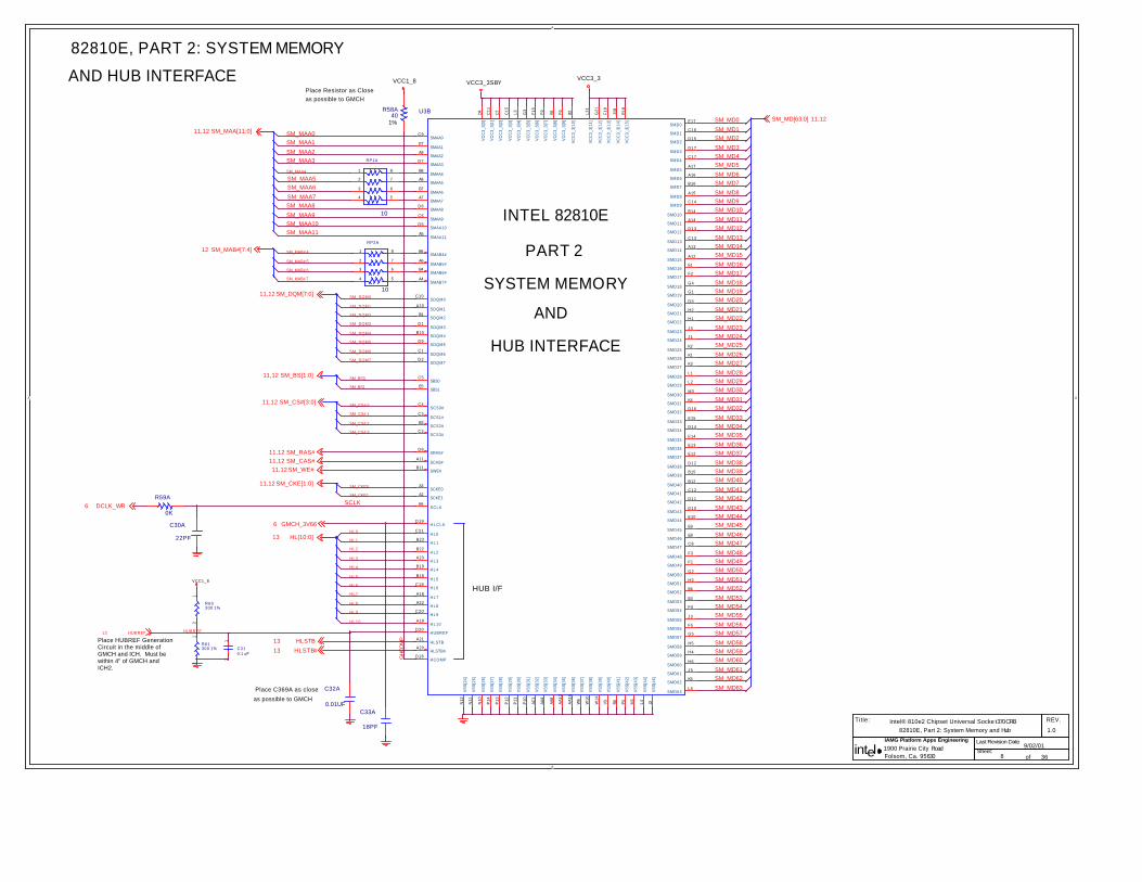
A
A
A A
82810E, PART 2: SYSTEM MEMORY
AND HUB INTERFACEas possible to GMCHPlace Resistor as Close
Place C369A as close
as possible to GMCH
Place HUBREF GenerationCircuit in the middle ofGMCH and ICH. Must bewithin 4" of GMCH andICH2.
Intel® 810e2 Chipset Universal Socke t 370 CRB82810E, Part 2: System Memory and Hub
36
1.0
9/02/01
8
IAMG Platform Apps Engineering1900 Prairie City RoadFolsom, Ca. 95630
REV.
Last Revision Date:
Sheet:of
Title:
intel
GH
CO
MP
SM_MD2
SM_MD33
SM_MD58
SM_MD61
SM_MD18
SM_MD42
SM_MD24SM_MD23
SM_MD29
SM_MD21
SM_MD48
SM_MD50
SM_MD7
SM_MD0
SM_MD46
SM_MD12
SM_MD54
SM_MD39
SM_MD10
SM_MD5
SM_MD37
SM_MD35
SM_MD14
SM_MD59
SM_MD30
SM_MD3
SM_MD34
SM_MD19
SM_MD62
SM_MD49
SM_MD15
SM_MD8
SM_MD51
SM_MD22
SM_MD57
SM_MD55
SM_MD25
SM_MD47
SM_MD40
SM_MD31
SM_MD44
SM_MD60
SM_MD32
SM_MD36
SM_MD17
SM_MD1
SM_MD27
SM_MD20
SM_MD28
SM_MD63
SM_MD6
SM_MD16
SM_MD9
SM_MD52
SM_MD11
SM_MD53
SM_MD13
SM_MD38
SM_MD4
SM_MD56
SM_MD43
SM_MD26
SM_MD41
SM_MD45
SCLK
SM_MAB# 7
SM_MAB# 6
SM_MAB# 5
SM_MAB# 4
SM_DQM0
SM_DQM1
SM_DQM2
SM_DQM3
SM_DQM4
SM_DQM5
SM_DQM6
SM_DQM7
SM_BS0
SM_BS1
SM_CS# 3
SM_CS# 2
SM_CS# 1
SM_CS# 0
SM_CKE0
SM_CKE1
HL0
HL1
HL2
HL3
HL4
HL5
HL6
HL9
HL10
HL8
HL7
SM_MAA8
SM_MAA5
SM_MAA1
SM_MAA7
SM_MAA6
SM_MAA9
SM_MAA3SM_MAA2
SM_MAA0
SM_MAA11SM_MAA10
SM_MAA4
HUBREF
SM_MAB#[7:4]12
SM_RAS#11,12SM_CAS#11,12SM_WE#11,12
GMCH_3V666
HLSTB13
HLSTB#13
SM_DQM[7:0]11,12
SM_BS[1:0]11,12
SM_CS#[3:0]11,12
SM_CKE[1:0]11,12
SM_MD[63:0] 11,12
HL[10:0]13
SM_MAA[11:0]11,12
DCLK_WR6
HUBREF13
VCC1_8 VCC3_3VCC3_3SBY
VCC1_8
R60300 1%
12
RP1A
10
1
2
3
4 5
6
7
8
R59A
0K
R61300 1%
12
RP2A
10
1
2
3
4 5
6
7
8
18PF
C33A
22PF
C30A
AND
SYSTEM MEMORY
HUB INTERFACE
HUB I/F
U3B
INTEL 82810E
PART 2
D18
C21
B23
A19
B22
A23
B19
B18
C18
A18
A22
C20
D19
A21
A20
D20
C5
A11
A3
A2
E6
C4
C3
B3
C2
C10
A10
B1
D1
B10
D9
C1
D2
C9
E7
D5
A5
A9
D7
B8
A8
B7
A7
D6
C6
B6
A6
B4
A4
E17
C16
B14
A14
D13
C13
A13
A12
E1
F2
G4
G1
D15
D3
H2
H1
J4
J1
K2
K1
K3
L1
L2
D17
M3
K4
D16
E15
D14
E14
E13
E12
D12
B15
C17
B12
C12
D11
D10
E10
E9
E8
C8
F3
F1
A17
G2
H3
E4
E3
F4
J3
F5
G5
H5
H4
A16
H6
J5
K5
L5
B16
A15
C14
D8
B11
D4 B2 L21
F18
J18
R18
C11
C7 C15
L3 G3
F15
F9
K6 F6
N12
N11
N10
P14
P13
P12
P11
P10
AC1
AA4
AA8
AA
12
AA
16
W6
W10
W14
V3 R6 P3 M1
L4 J2
E5
G21
HCOMP
HL0
HL1
HL10
HL2
HL3
HL4
HL5
HL6
HL7
HL8
HL9
H L C L K
HLSTB
HLSTB#
HUBREF
SBS0
SCAS#
SCKE0
SCKE1
SCLK
SCS0#
SCS1#
SCS2#
SCS3#
SDQM0
SDQM1
SDQM2
SDQM3
SDQM4
SDQM5
SDQM6
SDQM7
SMAA0
SMAA1
SMAA10
SMAA11
SMAA2
SMAA3
SMAA4
SMAA5
SMAA6
SMAA7
SMAA8
SMAA9
SMAB4#
SMAB5#
SMAB6#
SMAB7#
SMD0
SMD1
SMD10
SMD11
SMD12
SMD13
SMD14
SMD15
SMD16
SMD17
SMD18
SMD19
SMD2
SMD20
SMD21
SMD22
SMD23
SMD24
SMD25
SMD26
SMD27
SMD28
SMD29
SMD3
SMD30
SMD31
SMD32
SMD33
SMD34
SMD35
SMD36
SMD37
SMD38
SMD39
SMD4
SMD40
SMD41
SMD42
SMD43
SMD44
SMD45
SMD46
SMD47
SMD48
SMD49
SMD5
SMD50
SMD51
SMD52
SMD53
SMD54
SMD55
SMD56
SMD57
SMD58
SMD59
SMD6
SMD60
SMD61
SMD62
SMD63
SMD7
SMD8
SMD9
SRAS#
SWE#
VC
C3_
3[0]
VC
C3_
3[10
]
VC
C3_
3[11
]
VC
C3_
3[13
]
VC
C3_
3[14
]
VC
C3_
3[15
]
VC
C3_
3[1]
VC
C3_
3[2]
VC
C3_
3[3]
VC
C3_
3[4]
VC
C3_
3[5]
VC
C3_
3[6]
VC
C3_
3[7]
VC
C3_
3[8]
VC
C3_
3[9]
VS
S[2
4]
VS
S[2
5]
VS
S[2
6]
VS
S[2
7]
VS
S[2
8]
VS
S[2
9]
VS
S[3
0]
VS
S[3
1]
VS
S[3
2]
VS
S[3
3]
VS
S[3
4]
VS
S[3
5]
VS
S[3
6]
VS
S[3
7]
VS
S[3
8]
VS
S[3
9]
VS
S[4
0]
VS
S[4
1]
VS
S[4
2]
VS
S[4
3]
VS
S[4
4]
VS
S[4
5]
SBS1
VC
C3_
3[12
]
0.01UF
C32A
C310.1 uF
12
R58A40
1%

A
A
A A
Place as close asPossible to GMCHand via straight to
VSS plane.
GMCH RESET STRAPS
Place R242A within 0.5"of the GMCH Ball.
Use Surface Mount Caps
placed as close as possible topower pins with short,
wide direct connections
82810E, PART 3: DISPLAY CACHE
AND VIDEO INTERFACE
Jumper CommentFunction
XOR IN = XOR Tree
*OUT = NormalTri-state JP22A IN = Tri-state Mode
*OUT = Normal
Systembus freg
N/A Reads SystemBus Freq.
IOQ Depth JP23A IN = IOQ Depth of 1
*Out = IOQ Depth of 4VCOREDetect
RESVD
N/A
JP24A
Detects type of ProcessorI/O Buffers
TBD
Do not Stuff C374APlace site w / in 0.5"of clock ball (AA21).
JP21A
Do Not Populate C375A
LMD26 Processor Auto-Detect Circuit
Intel® 810e2 Chipset Universal Socke t 370 CRB
82810E, Part 3 : Display Cache and Video
36
1.0
9/02/01
9
IAMG Platform Apps Engineering1900 Prairie City RoadFolsom, Ca. 95630
REV.
Last Revision Date:
Sheet:of
Title:
intel
DC_MD 31
DC_MD30
DC_MD 28
DC_MD 26
GR
S_P
U26
GR
S_P
U28
GR
S_P
U30
DC_MD21
DC_MD29
VCCDACA
DC_MD14
DC_MD3
DC_MD6DC_MD7
RCLK
FTD10DC_MA2
DC_MD10
DC_MD15
DC_MD26
DC_MD12
DC_MD8
DC_MD9
FTD1
FTD2DC_DQM1
DC_DQM2
DC_MA11
DC_MD0
DC_MD5
DC_MA10
DC_MA3
DC_MA5
DC_MD25
FTD8
DC_MD17
FTD3
DC_MA8
DC_MD4
R_LT CLK
FTD0DC_DQM0
DC_MA0
DC_MD31
FTD9DC_MA1
DC_MA6
DC_MD11
DC_MD20
DC_MD22
OCLK
DC_DQM3
DC_MD13
DC_MD27
DC_MD30
FTD11
FTD4
DC_MA9
DC_MD24 IREFPD
DC_MD1
DC_MD16
DC_MD18
DC_MD23
FTD7
DC_MD13
DC_MA7
DC_MD2
FTD6
DC_MD29
DOTCLK
DC_MA4
DC_MD19
DC_MD28
FTD5
FREQSEL 6,31
FTBLNK# 24SL_STALL 24
DC_CLK10
DC_RAS#10DC_CAS#10
DC_WE#10
DC_CS#10
DC_DQM[3:0]10
DC_MA[11:0]10
DC_MD[31:0]10
FTD[11:0] 24
R_REFCLK 31
CRT_HSYNC 25
3VFTSCL 24,25
CRT_VSYNC 25
VID_RED 25
FTCLK1 24
DOTCLK 6
VID_BLUE 25
3VDDCCL 25
VID_GREEN 25
3VFTSDA 24,25
FTCLK0 24
FTHSYNC 24
FTVSYNC 24
3VDDCDA 25
VCC1_8 VCC1_8
VCC3_3
VCC3_3
TUAL5
DC_MD26
L7A
68NH-0.3A
22PF
C38A0.
01U
F
C34
A
+
33U
F
C36
A1
2
JP4A
0.1U
F
C35
A
RP4A
1 0 K
1 2 3 45678
JP5A
JP2A
R18.2K
JP3A
R63A
22
18PF
C 3 7 A
Q12N7002
R62A1741%
R65A
33
INTERFACE
VIDEO DIGITAL OUT
GRAPHICS INTERFACE
DISPLAY CACHE
U3C
AND
VIDEO INTERFACE
DISPLAY CACHE
INTEL 82810E
PART3
V19
AC23
V21
V22
AA21
W20
W19
AC22
AB20
AA23
Y23
K20
L20
P21
R23
C23
F20
M19
P19
M20
L19
P20
N19
J21
H19
H20
H18
G19
F19
M22
M21
P23
P22
N23
N21
N20
M23
F23
E20
E21
E23
L23
D22
D23
D21
C22
H21
H22
H23
G20
G22
G23
L22
F21
F22
K21
K23
R19
R20
R22
R21
J23
K19
J20
K22
T19
T20
Y21
Y20
T22
T21
W23
W22
W21
V23
U23
U22
U21
T23
J19
AC21
U20
U19
V20
E19
AC
20
AB
23
AB
21
U6
E18
AA
22
AB
22
T6
J6 G6
E2 A1 B5 B9 E11
B13
E16
B17
B21
G18
K18
P18
T18
AA
19
AA20
BLANK#
BLUE
CLKOUT0
CLKOUT1
DCLKREF
D D C C L
D D C D A
GREEN
HSYNC
IREF
IWASTE
LCAS#
LCS#
LDQM0
LDQM1
LDQM2
LDQM3
LMA0
LMA1
LMA10
LMA11
LMA2
LMA3
LMA4
LMA5
LMA6
LMA7
LMA8
LMA9
LMD0
LMD1
LMD10
LMD11
LMD12
LMD13
LMD14
LMD15
LMD16
LMD17
LMD18
LMD19
LMD2
LMD20
LMD21
LMD22
LMD23
LMD24
LMD25
LMD26
LMD27
LMD28
LMD29
LMD3
LMD30
LMD31
LMD4
LMD5
LMD6
LMD7
LMD8
LMD9
LOCLK
LRAS#
L R C L K
LTCLK
LTVCL
LTVDA
LTVDATA0
LTVDATA1
LTVDATA10
LTVDATA11
LTVDATA2
LTVDATA3
LTVDATA4
LTVDATA5
LTVDATA6
LTVDATA7
LTVDATA8
LTVDATA9
LWE#
RED
TVCLKIN/SL_STALL
TVHSYNC
TVVSYNC
VCC
BA
VCC
DA
VCC
DAC
A1
VCC
DAC
A2
VCC
HA
VSSB
A
VSSD
A
VSSD
ACA
VSSH
A
VS
S[4
6]
VS
S[4
7]
VS
S[4
8]
VS
S[4
9]
VS
S[5
0]
VS
S[5
1]
VS
S[5
2]
VS
S[5
3]
VS
S[5
4]
VS
S[5
5]
VS
S[5
6]
VS
S[5
7]
VS
S[5
8]
VS
S[5
9]
VS
S[6
0]
VS
S[6
1]
VSYNC
R64A
0K
RP3A
1 0 K
1 2 3 45678
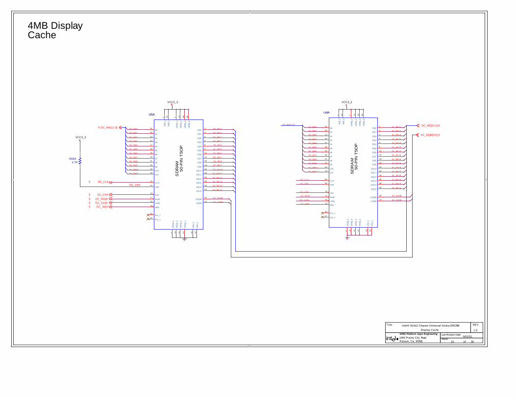
A
A
A A
4MB DisplayCache
Intel® 810e2 Chipset Universal Socke t 370 CRB
Display Cache
36
1.0
9/02/01
10
IAMG Platform Apps Engineering1900 Prairie City RoadFolsom, Ca. 95630
REV.
Last Revision Date:
Sheet:of
Title:
intel
DC_DQM2
DC_DQM3DC_DQM1
DC_DQM0
DC_MD 16
DC_MD 18
DC_MD 17
DC_MD 19
DC_MD 20
DC_MD 21
DC_MD 22
DC_MD 23
DC_MD 24
DC_MD 25
DC_MD 26
DC_MD 27
DC_MD 28
DC_MD 29
DC_MD 30
DC_MD 31
DC_MD 0
DC_MD 1
DC_MD 2
DC_MD 3
DC_MD 4
DC_MD 5
DC_MD 6
DC_MD 7
DC_MD 8
DC_MD 9
DC_MD10
DC_MD 11
DC_MD 12
DC_MD 13
DC_MD 14
DC_MD 15
D C _ W E#
DC_CAS#
DC_RAS#
D C _ C S#
D C _ C L K
DC_MA[11:0]
DC_CKEDC_CKE
DC_MA0
DC_MA1
DC_MA2
DC_MA3
DC_MA4
DC_MA5
DC_MA6
DC_MA7
DC_MA8
DC_MA9
DC_MA10
DC_MA11DC_MA1 1
DC_MA1 0
DC_MA9
DC_MA8
DC_MA7
DC_MA6
DC_MA5
DC_MA4
DC_MA3
DC_MA2
DC_MA1
DC_MA0
DC_DQM[3:0] 9
DC_CS#9
DC_RAS#9DC_CAS#9DC_WE#9
DC_CLK9
DC_MA[11:0]9DC_MD[31:0] 9
VCC3_3
VCC3_3
VCC3_3
50-P
IN T
SO
PS
DR
AM
U4A
21
22
20
19
23
24
27
28
29
30
31
32
35
2
3
42
43
45
46
48
49
5
6
8
9
11
12
39
40
14
33
37
36
7 13 38 441 25
4741104 5026
34
16
17
18
15
A0
A1
A10
A11
A2
A3
A4
A5
A6
A7
A8
A9
C L K
DQ0
DQ1
DQ10
DQ11
DQ12
DQ13
DQ14
DQ15
DQ2
DQ3
DQ4
DQ5
DQ6
DQ7
DQ8
DQ9
LDQM
NC_1
NC_2
UDQM
VD
DQ
_1
VD
DQ
_2
VD
DQ
_3
VD
DQ
_4
VD
D_1
VD
D_2
VS
SQ
_1
VS
SQ
_2
VS
SQ
_3
VS
SQ
_4
VS
S_1
VS
S_2
CKE
CAS#
RAS#
CS#
WE#
R66A4.7K
50-P
IN T
SO
PS
DR
AM
U5A
21
22
20
19
23
24
27
28
29
30
31
32
35
2
3
42
43
45
46
48
49
5
6
8
9
11
12
39
40
14
33
37
36
7 13 38 441 25
4741104 5026
34
16
17
18
15
A0
A1
A10
A11
A2
A3
A4
A5
A6
A7
A8
A9
C L K
DQ0
DQ1
DQ10
DQ11
DQ12
DQ13
DQ14
DQ15
DQ2
DQ3
DQ4
DQ5
DQ6
DQ7
DQ8
DQ9
LDQM
NC_1
NC_2
UDQM
VD
DQ
_1
VD
DQ
_2
VD
DQ
_3
VD
DQ
_4
VD
D_1
VD
D_2
VS
SQ
_1
VS
SQ
_2
VS
SQ
_3
VS
SQ
_4
VS
S_1
VS
S_2
CKE
CAS#
RAS#
CS#
WE#

A
A
A A
SYSTEM MEMORY
Intel® 810e2 Chipset Universal Socket 370 CRB
System Memory : DIMM0
36
1.0
9/02/01
11
IAMG Platform Apps Engineering1900 Prairie City RoadFolsom, Ca. 95630
REV.
Last Revision Date:
Sheet:of
Title:
intel
SM
_MD
40
SM
_MD
2
SM
_MD
26
SM
_MD
42
SM
_MD
32
SM
_MD
5
SM
_MD
25
SM
_MD
53
SM
_MD
43
SM
_MD
44
SM
_MD
51
SM
_MD
61
SM
_MD
12
SM
_MD
27
SM
_MD
16
SM
_MD
23
SM
_MD
41
SM
_MD
49
SM
_MD
8
SM
_MD
18
SM
_MD
28
SM
_MD
6
SM
_MD
54
SM
_MD
33
SM
_MD
31
SM
_MD
37
SM
_MD
45
SM
_MD
1
SM
_MD
13
SM
_MD
29
SM
_MD
9
SM
_MD
47
SM
_MD
50
SM
_MD
34
SM
_MD
38
SM
_MD
19
SM
_MD
55
SM
_MD
52
SM
_MD
30
SM
_MD
46
SM
_MD
24
SM
_MD
3
SM
_MD
0
SM
_MD
62
SM
_MD
7
SM
_MD
14
SM
_MD
59
SM
_MD
48
SM
_MD
11
SM
_MD
17
SM
_MD
39
SM
_MD
63
SM
_MD
21
SM
_MD
35
SM
_MD
20
SM
_MD
56
SM
_MD
36
SM
_MD
10
SM
_MD
58
SM
_MD
57
SM
_MD
22
SM
_MD
4
SM
_MD
60
SM
_MD
15
ME
MC
LK0
ME
MC
LK1
ME
MC
LK2
ME
MC
LK3
SM
_MA
A1
1
SM
_MA
A1
0
SM
_MA
A9
SM
_MA
A8
SM
_MA
A7
SM
_MA
A6
SM
_MA
A5
SM
_MA
A4
SM
_MA
A3
SM
_MA
A2
SM
_MA
A1
SM
_MA
A0
SM
_BS
1
SM
_BS
0
SM
_DQ
M7
SM
_DQ
M2
SM
_DQ
M4
SM
_DQ
M1
SM
_DQ
M6
SM
_DQ
M5
SM
_DQ
M3
SM
_DQ
M0
SM
_CS
#0
SM
_CS
#1
SM_C
KE0
SM_C
KE1
MEMCLK[7:0]6,12
SM_MAA[11:0]8,12
SM_BS[1:0]8,12
SM_DQM[7:0]8,12
SM_CS#[3:0]8,12SM_WE#8,12
SM_CAS#8,12SM_RAS#8,12
SM_CKE[1:0]8,12
SMBDATA12,14,16,25,26,32
SMBCLK12,14,16,25,26,32
SM_MD[63:0]8,12
SAO_PU 12
VCC3_3SBY
SOCKETDIMM168 PIN
J2A
33 117
38 123
126
132
34 118
35 119
36 120
37 121
122
39 111
128
63125
79 163
2 3 14 15 16 17 19 20 55 56 57 584 60 65 66 67 69 70 71 72 74 755 76 77 86 87 88 89 91 92 93 947 95 97 98 99 103
104
139
140
8 141
142
149
153
154
155
156
9 158
161
10 11
28 29 46 47 112
113
130
131
21 22 52 53 105
106
136
137
115
147
30 114
45 129
165
166
167
838227
1
12
23
32
43
54
64
68
78
85
96
107
116
127
138
148
152
162
24 25 31 44 48 50 51 61 62 8081 108
109
134
135
145
146
164
144
42
6
18
26
40
41
90
102
110
124
49
59
73
84
133
143
157
168
13 100
101
150
151
159
160
A0 A1 A10
A11
A12
A13
A2 A3 A4 A5 A6 A7 A8 A9 BA0
BA1
CAS
#
CKE
0
CKE
1
CLK
1
CLK
2
CLK
3
DQ
0
DQ
1
DQ
10
DQ
11
DQ
12
DQ
13
DQ
14
DQ
15
DQ
16
DQ
17
DQ
18
DQ
19
DQ
2
DQ
20
DQ
21
DQ
22
DQ
23
DQ
24
DQ
25
DQ
26
DQ
27
DQ
28
DQ
29
DQ
3
DQ
30
DQ
31
DQ
32
DQ
33
DQ
34
DQ
35
DQ
36
DQ
37
DQ
38
DQ
39
DQ
4
DQ
40
DQ
41
DQ
42
DQ
43
DQ
46
DQ
47
DQ
48
DQ
49
DQ
5
DQ
50
DQ
51
DQ
53
DQ
56
DQ
57
DQ
58
DQ
59
DQ
6
DQ
60
DQ
63
DQ
7
DQ
8
DQ
MB0
DQ
MB1
DQ
MB2
DQ
MB3
DQ
MB4
DQ
MB5
DQ
MB6
DQ
MB7
ECC0
ECC1
ECC2
ECC3
ECC4
ECC5
ECC6
ECC7
RAS
#
RE
GE
S0#
S1#
S2#
S3#
SA0
SA1
SA2
SM
BC
LK
SM
BD
ATA
WE#
VSS1
VSS2
VSS3
VSS4
VSS5
VSS6
VSS7
VSS8
VSS9
VSS10
VSS11
VSS12
VSS13
VSS14
VSS15
VSS16
VSS17
VSS18
NC1
NC2
NC3
NC4
NC5
NC6
NC7
NC8
NC9
NC
10
WP
NC
11
NC
12
NC
13
NC
14
NC
15
NC
16
NC
17
DQ
52
CLK
0
VCC1
VCC2
VCC3
VCC4
VCC5
VCC6
VCC7
VCC8
VCC9
VCC10
VCC11
VCC12
VCC13
VCC14
VCC15
VCC16
VCC17
DQ
9
DQ
44
DQ
45
DQ
54
DQ
55
DQ
61
DQ
62

A
A
A A
SYSTEM MEMORY
Intel® 810e2 Chipset Universal Socke t 370 CRBSystem Memory : DIMM1
36
1.0
9/02/01
12
IAMG Platform Apps Engineering1900 Prairie City RoadFolsom, Ca. 95630
REV.
Last Revision Date:
Sheet:of
Title:
intel
SM
_MD
0
SM
_MD
10
SM
_MD
63
SM
_MD
3
SM
_MD
32
SM
_MD
28
SM
_MD
58
SM
_MD
55
SM
_MD
43
SM
_MD
25
SM
_MD
22
SM
_MD
60
SM
_MD
49
SM
_MD
18
SM
_MD
15
SM
_MD
40
SM
_MD
50
SM
_MD
8
SM
_MD
5S
M_M
D6
SM
_MD
46
SM
_MD
12
SM
_MD
34
SM
_MD
31
SM
_MD
9
SM
_MD
2
SM
_MD
30
SM
_MD
27
SM
_MD
45
SM
_MD
57
SM
_MD
61
SM
_MD
24
SM
_MD
42
SM
_MD
20S
M_M
D21
SM
_MD
52
SM
_MD
54
SM
_MD
37
SM
_MD
17
SM
_MD
39
SM
_MD
14
SM
_MD
1
SM
_MD
48
SM
_MD
53
SM
_MD
11
SM
_MD
4
SM
_MD
33
SM
_MD
29
SM
_MD
59
SM
_MD
26
SM
_MD
23
SM
_MD
44
SM
_MD
56
SM
_MD
62
SM
_MD
19
SM
_MD
41
SM
_MD
51
SM
_MD
7
SM
_MD
35
SM
_MD
38
SM
_MD
16
SM
_MD
13
SM
_MD
36
SM
_MD
47
ME
MC
LK5
ME
MC
LK7
ME
MC
LK6
ME
MC
LK4
SM
_MA
A0
SM
_MA
A1
SM
_MA
A2
SM
_MA
A3
SM
_MA
B#
4
SM
_MA
B#
5
SM
_MA
B#
6
SM
_MA
B#7
SM
_MA
A8
SM
_MA
A9
SM
_MA
A1
0
SM
_MA
A1
1
SM
_BS
0
SM
_BS
1
SM
_DQ
M7
SM
_DQ
M6
SM
_DQ
M5
SM
_DQ
M4
SM
_DQ
M3
SM
_DQ
M2
SM
_DQ
M1
SM
_DQ
M0
SM
_CS
#2
SM
_CS
#3
SM_C
KE0
SM_C
KE1
SAO_PU
MEMCLK[7:0]6,11
SM_MAA[11:0]8,11
SM_MAB#[7:4]8
SM_BS[1:0]8,11
SM_DQM[7:0]8,11
SM_CS#[3:0]8,11
SM_WE#8,11
SM_CAS#8,11SM_RAS#8,11
SM_CKE[1:0]8,11
SMBDATA11,14,16,25,26,32SMBCLK11,14,16,25,26,32
SM_MD[63:0]8,11
SAO_PU 11
VCC3_3SBY
VCC3_3SBY
SOCKETDIMM168 PIN
J3A
33 117
38 123
126
132
34 118
35 119
36 120
37 121
122
39 111
128
63125
79 163
2 3 14 15 16 17 19 20 55 56 57 584 60 65 66 67 69 70 71 72 74 755 76 77 86 87 88 89 91 92 93 947 95 97 98 99 103
104
139
140
8 141
142
149
153
154
155
156
9 158
161
10 11
28 29 46 47 112
113
130
131
21 22 52 53 105
106
136
137
115
147
30 114
45 129
165
166
167
838227
1
12
23
32
43
54
64
68
78
85
96
107
116
127
138
148
152
162
24 25 31 44 48 50 51 61 62 8081 108
109
134
135
145
146
164
144
42
6
18
26
40
41
90
102
110
124
49
59
73
84
133
143
157
168
13 100
101
150
151
159
160
A0 A1 A10
A11
A12
A13
A2 A3 A4 A5 A6 A7 A8 A9 BA0
BA1
CAS
#
CKE
0
CKE
1
CLK
1
CLK
2
CLK
3
DQ
0
DQ
1
DQ
10
DQ
11
DQ
12
DQ
13
DQ
14
DQ
15
DQ
16
DQ
17
DQ
18
DQ
19
DQ
2
DQ
20
DQ
21
DQ
22
DQ
23
DQ
24
DQ
25
DQ
26
DQ
27
DQ
28
DQ
29
DQ
3
DQ
30
DQ
31
DQ
32
DQ
33
DQ
34
DQ
35
DQ
36
DQ
37
DQ
38
DQ
39
DQ
4
DQ
40
DQ
41
DQ
42
DQ
43
DQ
46
DQ
47
DQ
48
DQ
49
DQ
5
DQ
50
DQ
51
DQ
53
DQ
56
DQ
57
DQ
58
DQ
59
DQ
6
DQ
60
DQ
63
DQ
7
DQ
8
DQ
MB0
DQ
MB1
DQ
MB2
DQ
MB3
DQ
MB4
DQ
MB5
DQ
MB6
DQ
MB7
ECC0
ECC1
ECC2
ECC3
ECC4
ECC5
ECC6
ECC7
RAS
#
RE
GE
S0#
S1#
S2#
S3#
SA0
SA1
SA2
SM
BC
LK
SM
BD
ATA
WE#
VSS1
VSS2
VSS3
VSS4
VSS5
VSS6
VSS7
VSS8
VSS9
VSS10
VSS11
VSS12
VSS13
VSS14
VSS15
VSS16
VSS17
VSS18
NC1
NC2
NC3
NC4
NC5
NC6
NC7
NC8
NC9
NC
10
WP
NC
11
NC
12
NC
13
NC
14
NC
15
NC
16
NC
17
DQ
52
CLK
0
VCC1
VCC2
VCC3
VCC4
VCC5
VCC6
VCC7
VCC8
VCC9
VCC10
VCC11
VCC12
VCC13
VCC14
VCC15
VCC16
VCC17
DQ
9
DQ
44
DQ
45
DQ
54
DQ
55
DQ
61
DQ
62
R 6 7 A
2.2K
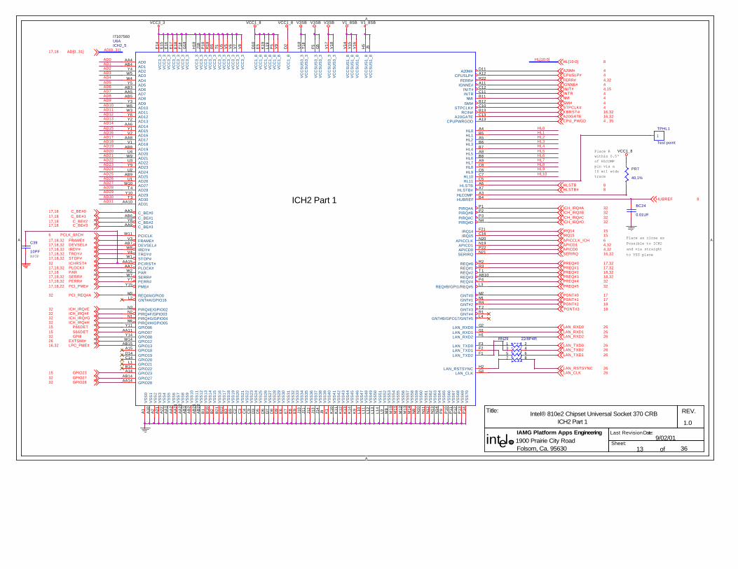
A
A
A A
Place Rwithin 0.5"of HLCOMPpin via a10 mil widetrace
Place as close asPossible to ICH2and via straightto VSS planeNPOP
ICH2 Part 1
Intel® 810e2 Chipset Universal Socket 370 CRBICH2 Part 1
36
1.0
9/02/01
13
IAMG Platform Apps Engineering1900 Prairie City RoadFolsom, Ca. 95630
REV.
R
Last Revision Date:
Sheet:of
Title:
intel
HL[10:0]
AD[0..31]
HL0
HL5
AD31
AD0
AD12
AD14AD15
AD17
AD19
AD30
HL1
HL7
HL10
AD13
AD23
AD28
AD7
HL2
HL4
AD4
AD6
AD8
AD22HL8
AD9
AD26
HL9
AD16
AD18
AD21
HL3
AD3
HL6
AD1
AD5
AD27
AD20
AD29
AD2
AD10AD11
AD24AD25
KBRST# 16,32A20GATE 16,32
FERR# 4,32
CPU_PWGD 4 , 35
HL[10:0] 8
LAN_RSTSYNC 26
A20M# 4
INTR 4INIT# 4,15
NMI 4SMI# 4STPCLK# 4
AD[0..31]17,18
LAN_TXD0 26
LAN_TXD1 26LAN_TXD2 26
GPIO2832
PCI_REQ#A32
TRDY#17,18,32
IRQ15 15
ICH_IRQ#E32
EXTSMI#26
C_BE#217,18ICH_IRQ#C 32ICH_IRQ#D 32
FRAME#17,18,32
PREQ#0 17,32
PGNT#2 18
STOP#17,18,32
LAN_RXD1 26
GPIO2315
LPC_PME#16,32
ICH_IRQ#G32
PCLK_0/ICH6
PREQ#5 32
C_BE#317,18
PAR17,18PLOCK#17,18,32
DEVSEL#17,18,32
SERIRQ 16,32
PGNT#0 17
ICH_IRQ#F32
C_BE#017,18
PREQ#1 17,32PREQ#2 18,32
GPI832S66DET15
PCI_PME#17,18,22
ICH_IRQ#A 32ICH_IRQ#B 32
PERR#17,18,32
P66DET15
PREQ#3 18,32
LAN_RXD0 26ICH_IRQ#H32
C_BE#117,18
HLSTB 8
IRQ14 15
APICD1 4,32
SERR#17,18,32
IRDY#17,18,32
APICCLK_ICH 6
PGNT#1 17
PREQ#4 32
GPIO2732
HLSTB# 8
APICD0 4,32
PGNT#3 18
IGNNE# 4
ICHRST#32
CPUSLP# 4
LAN_CLK 26
LAN_RXD2 26
HUBREF 8
V1_8SB V1_8SBV3SBV3SB V3SBVCC1_8VCC3_3
VCC1_8
VCC1_8
RN29 22/8P4R1357
2468
C39
10PF
TPHL1
Test point
1
PR7
40,1%
BC24
0.01UF
U6AICH2_5
I7107560
AA4AB4
Y4W5W4Y5
AB3AA5AB5
Y3W6W3Y6Y2
AA6Y1V2
AA8V1
AB8U4
W9U3Y9U2
AB9U1
W10T 4
Y10T 3
AA10
AA3AB6
Y8AA9
W11V3
AB7W8V4
W1AA15
AA7W2W7
Y15
M3L2
E14
E15
E16
E17
E18
F18
G18
H18
J18
P18
R18
R5
T5 U5
V5
D11A12R22A11C12C11B11B12C10B13C13
A4B5A5B6B7A8B8A9C8C6C7
A6A7A3B4
P1P2P3N4
F21C16N20N19P22N21
R2R3T 1AB10
M2M1R4T 2
D10
E5
K19
L19
P5
V9
D2
Y7
N3N2N1
AA11Y14
W14AB15
A15D14C14
L1B14A14
AB14AA14
A13
C5
M4
P4L3
R1L4
A1
A10
A2
A21
A22
AA
1A
A2
AA
21A
A22
AB
1A
B2
AB
21A
B22
B1
B10
B2
B21
B22
B3
B9
C2
C3
C4
C9
D3
D5
D6
D7
D8
D9
E6
E7
E8
E9
J10
J11
J12
J13
J14
J9 K1
K10
K11
K12
K13
K14
K9
L10
L11
L12
L13
L14
L9 M9
M10
M11
M12
M13
M14
N9
N10
N11
N12
N13
N14
P9
P10
P11
P12
P13
P14
G2G1H1
F3F2F1
G3H2
V6
V7
V8
U18
T18
F5 G5
V17
V18
V14
V15
V16
H5
J5
Y11
AD0AD1AD2AD3AD4AD5AD6AD7AD8AD9AD10AD11AD12AD13AD14AD15AD16AD17AD18AD19AD20AD21AD22AD23AD24AD25AD26AD27AD28AD29AD30AD31
C_BE#0C_BE#1C_BE#2C_BE#3
PCICLKFRAME#DEVSEL#IRDY#TRDY#STOP#PCIRST#PLOCK#PARSERR#
PME#
REQ#A/GPIO0GNT#A/GPIO16
VC
C3_
3V
CC
3_3
VC
C3_
3V
CC
3_3
VC
C3_
3V
CC
3_3
VC
C3_
3
VC
C3_
3V
CC
3_3
VC
C3_
3V
CC
3_3
VC
C3_
3V
CC
3_3
VC
C3_
3V
CC
3_3
A20M#CPUSLP#
FERR#IGNNE#
INIT#INTR
NMISMI#
STPCLK#RCIN#
A20GATE
HL0HL1HL2HL3HL4HL5HL6HL7HL8HL9
HL10
HLSTBHLSTB#HLCOMPHUBREF
PIRQ#APIRQ#BPIRQ#CPIRQ#D
IRQ14IRQ15
APICCLKAPICD1APICD0SERIRQ
REQ#0REQ#1REQ#2REQ#3
GNT#0GNT#1GNT#2GNT#3
VC
C1_
8V
CC
1_8
VC
C1_
8V
CC
1_8
VC
C1_
8V
CC
1_8
VC
C1_
8PERR#
PIRQ#E/GPIO02PIRQ#F/GPIO03PIRQ#G/GPIO04
GPIO07GPIO08GPIO12GPIO13GPIO18GPIO19GPIO20GPIO21GPIO22GPIO23GPIO27GPIO28
CPUPWRGOD
HL11
PIRQ#H/GPIO05
REQ#4REQ#B/GPI1/REQ#5
GNT#4GNT#B/GPO17/GNT#5
VS
S0
VS
S1
VS
S2
VS
S3
VS
S4
VS
S5
VS
S6
VS
S7
VS
S8
VS
S9
VS
S10
VS
S11
VS
S12
VS
S13
VS
S14
VS
S15
VS
S16
VS
S17
VS
S18
VS
S19
VS
S20
VS
S21
VS
S22
VS
S23
VS
S24
VS
S25
VS
S26
VS
S27
VS
S28
VS
S29
VS
S30
VS
S31
VS
S32
VS
S33
VS
S34
VS
S35
VS
S36
VS
S37
VS
S38
VS
S39
VS
S40
VS
S41
VS
S42
VS
S43
VS
S44
VS
S45
VS
S46
VS
S47
VS
S48
VS
S49
VS
S50
VS
S51
VS
S52
VS
S53
VS
S54
VS
S55
VS
S56
VS
S57
VS
S58
VS
S59
VS
S60
VS
S61
VS
S62
VS
S63
VS
S64
VS
S65
VS
S66
VS
S67
VS
S68
VS
S69
VS
S70
LAN_RXD0LAN_RXD1LAN_RXD2
LAN_TXD0LAN_TXD1LAN_TXD2
LAN_CLKLAN_RSTSYNC
VC
C3_
3V
CC
3_3
VC
C3_
3
VC
CS
US
3_3
VC
CS
US
3_3
VC
CS
US
3_3
VC
CS
US
3_3
VC
CS
US
3_3
VC
CS
US
3_3
VC
CS
US
1_8
VC
CS
US
1_8
VC
CS
US
1_8
VC
CS
US
1_8
VC
CS
US
1_8
GPIO06
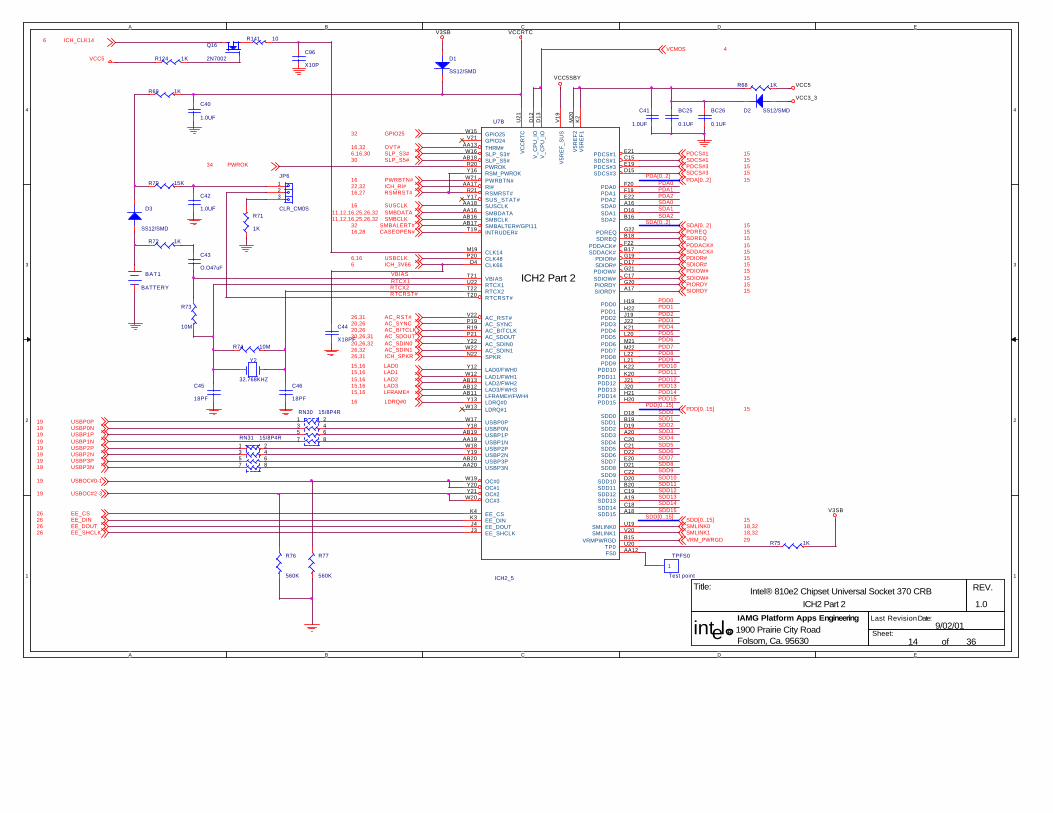
A
A
B
B
C
C
D
D
E
E
4 4
3 3
2 2
1 1
ICH2 Part 2
Intel® 810e2 Chipset Universal Socket 370 CRBICH2 Part 2
36
1.0
9/02/01
14
IAMG Platform Apps Engineering1900 Prairie City RoadFolsom, Ca. 95630
REV.
R
Last Revision Date:
Sheet:of
Title:
intel
SDA[0..2]
PDD[0..15]
PDA[0..2]
PDA2
SDD8
RTCX2
PDA0
PDD13
SDD3SDD4
VBIASRTCX1
SDA0
PDD15
SDD12
PDD4
PDD7
SDD9
PDA1
SDA1
PDD2
PDD6
SDD6
SDD13
SDA2
PDD8
PDD11PDD12
SDD2
PDD9PDD10
SDD1
SDD7
SDD15
PDD0
PDD14
SDD0
SDD5
SDD14
SDD11
PDD1
PDD3
SDD10
SDD[0..15]
RTCRST#
PDD5
SDCS#1 15
SDCS#3 15
PDIOR# 15
PDIOW# 15
SDDACK# 15
SDIOW# 15
PDREQ 15
SDIOR# 15
PIORDY 15
PDCS#1 15
AC_SDIN020,26,32
PDCS#3 15
SIORDY 15
PDDACK# 15SDREQ 15
ICH_SPKR26,31
AC_SYNC20,26
SDD[0..15] 15
PDD[0..15] 15
SLP_S3#6,16,30
PWRBTN#16
RSMRST#16,27
LAD215,16
SMBDATA11,12,16,25,26,32SUSCLK16
USBP1P19USBP1N19
USBP0N19
USBP2P19
USBP3P19USBP3N19
USBP2N19
EE_CS26
EE_SHCLK26
USBP0P19
USBOC#0-119
VCMOS 4
ICH_CLK146
PDA[0..2] 15
SDA[0..2] 15
USBOC#2-319
EE_DOUT26EE_DIN26
ICH_RI#22,32
SMLINK0 18,32
VRM_PWRGD 29
ICH_3V666
SLP_S5#30
LAD115,16
SMLINK1 18,32
OVT#16,32
CASEOPEN#16,28
LFRAME#15,16
LDRQ#016
SMBCLK11,12,16,25,26,32
AC_SDOUT20,26,31
SMBALERT#32
AC_BITCLK20,26
USBCLK6,16
LAD015,16
AC_RST#26,31
AC_SDIN126,32
GPIO2532
LAD315,16
PWROK34
VCC5
VCC3_3
V3SB
V3SB
VCC5SBY
VCCRTC
VCC5
R72 1K
10R141
C42
1.0UF
JP6
CLR_CM0S
1
32
D2 SS12/SMD
U7B
ICH2_5
AA13W16
AB18R20
W21AA17
R21Y17
AA16AB16AB17
T19
M19P20
D4
T21U22T22T20
V22P19R19P21Y22
W22N22
Y12W12
AB13AB12AB11
Y13W13
AB19AA19
W17Y18
Y20W19
E21C15E19D15
F20F19E22A16D16B16
G22B18F22B17G19D17G21C17G20A17
H19H22J19J22K21L20M21M22L22L21K22K20J21J20H21H20
D18B19D19A20C20C21D22E20D21C22D20B20C19A19C18A18
U21
M20
K2
V19
D13
D12
W15V21
Y16
W18Y19
AB20AA20
Y21W20
K4K3J4J3
U19V20B15U20
AA18
AA12
THRM#SLP_S3#SLP_S5#PWROK
PWRBTN#RI#RSMRST#SUS_STAT#
SMBDATASMBCLKSMBALTER#/GPI11INTRUDER#
CLK14CLK48CLK66
VBIASRTCX1RTCX2RTCRST#
AC_RST#AC_SYNCAC_BITCLKAC_SDOUTAC_SDIN0AC_SDIN1SPKR
LAD0/FWH0LAD1/FWH1LAD2/FWH2LAD3/FWH3LFRAME#/FWH4LDRQ#0LDRQ#1
USBP1PUSBP1N
USBP0PUSBP0N
OC#1OC#0
PDCS#1SDCS#1PDCS#3SDCS#3
PDA0PDA1PDA2SDA0SDA1SDA2
PDREQSDREQ
PDDACK#SDDACK#
PDIOR#SDIOR#
PDIOW#SDIOW#PIORDYSIORDY
PDD0PDD1PDD2PDD3PDD4PDD5PDD6PDD7PDD8PDD9
PDD10PDD11PDD12PDD13PDD14PDD15
SDD0SDD1SDD2SDD3SDD4SDD5SDD6SDD7SDD8SDD9
SDD10SDD11SDD12SDD13SDD14SDD15
VC
CR
TC
V5R
EF
2V
5RE
F1
V5R
EF
_SU
S
V_C
PU
_IO
V_C
PU
_IOGPIO25
GPIO24
RSM_PWROK
USBP2PUSBP2NUSBP3PUSBP3N
OC#2OC#3
EE_CSEE_DINEE_DOUTEE_SHCLK
SMLINK0SMLINK1
VRMPWRGDTP0
SUSCLK
FS0
Y2
32.768KHZ
BC26
0.1UF
D1
SS12/SMD
D3
SS12/SMD
TPFS0
Test point
1
C96
X10P
BC25
0.1UF
BAT1
BATTERY
RN31 15/8P4R1357
2468
R75 1K
R73
10M
R77
560K
C45
18PF
R69 1K
C46
18PF
Q16
2N7002
C41
1.0UF
R74 10M
RN30 15/8P4R1357
2468
C44
X18PF
R71
1K
R124 1K
R76
560K
C43
O.O47uF
C40
1.0UF
R70 15K
R68 1K

8
8
7
7
6
6
5
5
4
4
3
3
2
2
1
1
D D
C C
B B
A A
IDEFWH
Intel® 810e2 Chipset Universal Socket 370 CRBFWH & ULTRA-ATA100 IDE connectors
36
1.0
9/02/0115
IAMG Platform Apps Engineering1900 Prairie City RoadFolsom, Ca. 95630
REV.
R
Last Revision Date:
Sheet:of
Title:
intel
PDD8PDD6 PDD9PDD5 PDD10PDD4 PDD11PDD3 PDD12PDD2 PDD13PDD1 PDD14PDD0 PDD15
PDA1PDA0
SDD6SDD5SDD4SDD3SDD2SDD1SDD0
SDA1SDA0
SDA2
IDERST#
SDD11
SDD13
SDD9SDD10
SDD8
SDD15SDD14
SDD12
IDERST#SDD7
SDD[0..15]
SDA[0..2]
PDD7
PDA2
PDD[0..15]
PDA[0..2]
PDREQ14
PDIOR#14PDIOW#14
PIORDY14PDDACK#14
IRQ1413
PDCS#3 14
SDD[0..15]14
SDCS#114
SDA[0..2]14
SDIOW#14
SIORDY14SDDACK#14
IRQ1513
SDCS#3 14
SDIOR#14
IDEACTS#26
IDEACTP#26PDCS#114
SDREQ14
PCIRST#7,16,24,32
INIT# 4,13
LAD3 14,16
PCLK_6 6
GPIO2313
LAD014,16LAD114,16LAD214,16
LFRAME# 14,16
IDERST#32
PDD[0..15]14
PDA[0..2]14
S66DET 13
P66DET 13
VCC3_3
VCC3_3
VCC3_3
VCC3_3VCC3_3
VCC3_3
R78 33
U8
FWH32
123456789
10111213141516 17
181920212223242526272829303132VPP
RST#FGPI3FGPI2FGPI1FGPI0WP#TBL#ID3ID2ID1ID0FWH0FWH1FWH2GND FWH3
RFURFURFURFURFU
FWH4INIT#VCCGND
VCCAGNDA
ICFGPI4
CLKVCC
IDE2
PIN_2X20
13579
11131517192123252729
24681012141618202224262830
3133353739
3234363840
C48
47PF
IDE1
PIN_2X20
13579
11131517192123252729
24681012141618202224262830
3133353739
3234363840
R83 8.2K
R81 8.2K
BC28
0.1UF
R84
10K
R88
10K
R87 8.2K
BC29
0.1UF
BC27
0.1UF
R80
4.7K
BC30
0.1UF
R79
0
R85 33
R82 8.2K
R86
4.7K
C47
47PF
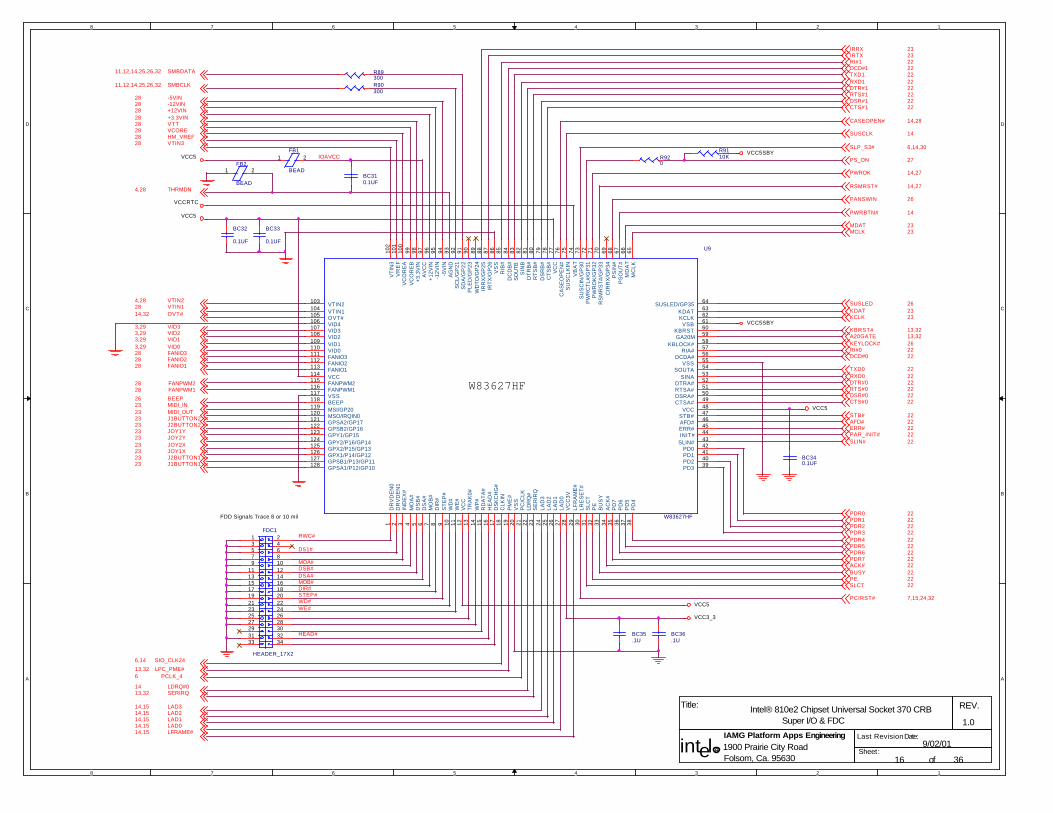
8
8
7
7
6
6
5
5
4
4
3
3
2
2
1
1
D D
C C
B B
A A
W83627HF
FDD Signals Trace 8 or 10 mil
Intel® 810e2 Chipset Universal Socket 370 CRBSuper I/O & FDC
36
1.0
9/02/01
16
IAMG Platform Apps Engineering1900 Prairie City RoadFolsom, Ca. 95630
REV.
R
Last Revision Date:
Sheet:of
Title:
intel
RWC#
STEP#
DSB#
DIR#
MOA#
DS1#
WD#
DSA#MOB#
HEAD#
WE#
IOAVCC
SUSLED 26KDAT 23KCLK 23
KEYLOCK# 26RI#0 22DCD#0 22
RXD0 22DTR#0 22RTS#0 22DSR#0 22CTS#0 22
STB# 22AFD# 22ERR# 22
ACK# 22BUSY 22PE 22
VTIN24,28VTIN128
FANIO328FANIO228FANIO128
FANPWM228FANPWM128
BEEP26
MCLK 23MDAT 23
PS_ON 27
IRRX 23IRTX 23RI#1 22DCD#1 22
RXD1 22DTR#1 22RTS#1 22DSR#1 22CTS#1 22
CASEOPEN# 14,28
SUSCLK 14
TXD1 22
KBRST# 13,32
MIDI_IN23
J1BUTTON223J2BUTTON223
J2BUTTON123J1BUTTON123
JOY1Y23JOY2Y23
MIDI_OUT23
JOY2X23JOY1X23
SMBDATA11,12,14,25,26,32
SLP_S3# 6,14,30
A20GATE 13,32
PWROK 14,27
SLCT 22
PCIRST# 7,15,24,32
HM_VREF28VTIN328
THRMDN4,28
SMBCLK11,12,14,25,26,32
OVT#14,32
PWRBTN# 14
PDR0 22PDR1 22PDR2 22PDR3 22
PDR5 22PDR6 22PDR7 22
LAD214,15LAD314,15
LAD114,15LAD014,15
SIO_CLK246,14
LPC_PME#13,32PCLK_46
LDRQ#014
VID03,29VID13,29VID23,29
-5VIN28-12VIN28+12VIN28
VTT28+3.3VIN28
VCORE28
LFRAME#14,15
SERIRQ13,32
PANSWIN 26
PDR4 22
RSMRST# 14,27
VID33,29
SLIN# 22
TXD0 22
PAR_INIT# 22
VCC5
VCC5
VCC5SBY
VCC3_3
VCC5
VCC5
VCCRTC
VCC5SBY
FB1
BEAD
1 2
BC36.1U
BC35.1U
BC32
0.1UF
R920
BC33
0.1UF
R89300
U9
W83627HF
1 2 3 4 5 6 7 9 10 11 12 13 14 16 17 18 19 20 21 22 23 24 25 26 27 28 29 30 31 32 33 34 35 36 37 38
3940414243444546474849505152535455565758596061626364
6566676869707172737475767778798081828384858687888990919293949596979899100
101
102
103104105106107108109110111112113114115116117118119120121122123124125126127128
8 15
DR
VD
EN
0D
RV
DE
N1
IND
EX
#M
OA
#D
SB
#D
SA
#M
OB
#
ST
EP
#W
D#
WE
#V
CC
TR
AK
0#W
P#
HE
AD
#D
SK
CH
G#
CLK
INP
ME
#V
SS
PC
ICLK
LDR
Q#
SE
RIR
QLA
D3
LAD
2LA
D1
LAD
0V
CC
3VLF
RA
ME
#LR
ES
ET
#S
LCT
PE
BU
SY
AC
K#
PD
7P
D6
PD
5P
D4
PD3PD2PD1PD0
SLIN#INIT#ERR#AFD#STB#
VCCCTSA#DSRA#RTSA#DTRA#
SINASOUTA
VSSDCDA#
RIA#KBLOCK#
GA20MKBRST
VSBKCLKKDAT
SUSLED/GP35
MC
LKM
DA
TP
SO
UT
#P
SIN
#C
IRR
X/G
P34
RS
MR
ST
#/G
P33
PW
RO
K/G
P32
PW
RC
TL#
/GP
31S
US
CIN
/GP
30V
BA
TS
US
CLK
INC
AS
EO
PE
N#
VC
CC
TS
B#
DS
RB
#R
TS
B#
DT
RB
#S
INB
SO
UTB
DC
DB
#R
IB#
VS
SIR
TX
/GP
26IR
RX
/GP
25W
DTO
/GP
24P
LED
/GP
23S
DA
/GP
22S
CL/
GP
21A
GN
D-5
VIN
-12V
IN+1
2VIN
AV
CC
+3.3
VIN
VC
OR
EB
VC
OR
EA
VR
EF
VT
IN3
VTIN2VTIN1OVT#VID4VID3VID2VID1VID0FANIO3FANIO2FANIO1VCCFANPWM2FANPWM1VSSBEEPMSI/GP20MSO/IRQIN0GPSA2/GP17GPSB2/GP16GPY1/GP15GPY2/P16/GP14GPX2/P15/GP13GPX1/P14/GP12GPSB1/P13/GP11GPSA1/P12/GP10
DIR
#
RD
AT
A#
FDC1
HEADER_17X2
13579
11131517192123252729
24681012141618202224262830
3133
3234
BC310.1UF
R90300
BC340.1UF
FB2
BEAD
1 2
R9110K

A
A
B
B
C
C
D
D
E
E
4 4
3 3
2 2
1 1
Intel® 810e2 Chipset Universal Socket 370 CRB
PCI 1 & 2
36
1.0
9/02/01
17
IAMG Platform Apps Engineering1900 Prairie City RoadFolsom, Ca. 95630
REV.
R
Last Revision Date:
Sheet:of
Title:
intel
AD30
AD28AD26
AD24
AD22AD20
AD18AD16
AD15
AD13AD11
AD9
AD6AD4
AD2AD0
AD31AD29
AD27AD25
AD23
AD21AD19
AD17
PERR#
AD14
AD12AD10
AD8AD7
AD5AD3
AD1
ACK64#
PIRQ#BPIRQ#D
PCI_RST#
PCI_PME#AD30
AD28AD26
AD24R_AD17
AD22AD20
AD18AD16
FRAME#
TRDY#
STOP#
PARAD15
AD13AD11
AD9
C_BE#0
AD6AD4
AD2AD0
PIRQ#CPIRQ#A
AD31AD29
AD27AD25
C_BE#3AD23
AD21AD19
AD17C_BE#2
IRDY#
DEVSEL#
PLOCK#PERR#
SERR#
C_BE#1AD14
AD12AD10
AD8AD7
AD5AD3
AD1
ACK64#
AD17R_AD16 AD16
AD[0..31]
C_BE#[0..3]
C_BE#3
C_BE#2
C_BE#1
C_BE#0
PIRQ#B18,32PIRQ#D18,32
PCLK_16
PREQ#013,32
IRDY#13,18,32
DEVSEL#13,18,32
PLOCK#13,18,32
SERR#13,18,32
AD[0..31]13,18
C_BE#[0..3]13,18
PIRQ#A 18,32PIRQ#C 18,32
PGNT#0 13
PCI_PME# 13,18,22
FRAME# 13,18,32
TRDY# 13,18,32
STOP# 13,18,32
PAR 13,18
ACK64#18,32
PGNT#1 13PREQ#113,32
PCLK_26PCI_RST# 18,32
PERR#13,18,32
REQ64#1 32 REQ64#2 32
VCC3_3
VCC5
VCC12VCC12-
VCC5
VCC3_3VCC3_3
VCC5
VCC12VCC12-
VCC5
VCC3_3
V3SBV3SB
PCI2
PCI_CON_32BIT
A1A2A3A4A5A6A7A8A9A10A11A12A13A14A15A16A17A18A19A20A21A22A23A24A25A26A27A28A29A30A31A32A33A34A35A36A37A38A39A40A41A42A43A44A45A46A47A48A49
A52A53A54A55A56A57A58A59A60A61A62
B1B2B3B4B5B6B7B8B9
B10B11B12B13B14B15B16B17B18B19B20B21B22B23B24B25B26B27B28B29B30B31B32B33B34B35B36B37B38B39B40B41B42B43B44B45B46B47B48B49
B52B53B54B55B56B57B58B59B60B61B62
TRST#+12VTMSTDI+5V
INTA#INTC#
+5VRESERVED
+5V(I/O)RESERVED
GNDGND
RESERVEDRST#
+5V(I/O)GNTGND
PME#AD30+3.3VAD28AD26GND
AD24IDSEL
+3.3AD22AD20GND
AD18AD16+3.3V
FRAME#GND
TRDY#GND
STOP#+3.3V
SDONESBO#
GNDPAR
AD15+3.3VAD13AD11GNDAD9
C/BE#0+3.3V
AD6AD4GNDAD2AD0
+5V(I/O)REQ64#
+5V+5V
-12VTCKGNDTDO+5V+5VINTB#INTD#PRSNT#1RESERVEDPRSNT#2GNDGNDRESERVEDGNDCLKGNDREQ#+5V(I/O)AD31AD29GNDAD27AD25+3.3VC/BE#3AD23GNDAD21AD19+3.3VAD17C/BE#2GNDIRDY#+3.3VDEVSEL#GNDLOCK#PERR#+3.3VSERR#+3.3VC/BE#1AD14GNDAD12AD10GND
AD8AD7+3.3VAD5AD3GNDAD1+5V(I/O)ACK64#+5V+5V
R94100
PCI1
PCI_CON_32BIT
A1A2A3A4A5A6A7A8A9A10A11A12A13A14A15A16A17A18A19A20A21A22A23A24A25A26A27A28A29A30A31A32A33A34A35A36A37A38A39A40A41A42A43A44A45A46A47A48A49
A52A53A54A55A56A57A58A59A60A61A62
B1B2B3B4B5B6B7B8B9
B10B11B12B13B14B15B16B17B18B19B20B21B22B23B24B25B26B27B28B29B30B31B32B33B34B35B36B37B38B39B40B41B42B43B44B45B46B47B48B49
B52B53B54B55B56B57B58B59B60B61B62
TRST#+12VTMSTDI+5V
INTA#INTC#
+5VRESERVED
+5V(I/O)RESERVED
GNDGND
RESERVEDRST#
+5V(I/O)GNTGND
PME#AD30+3.3VAD28AD26GND
AD24IDSEL
+3.3AD22AD20GND
AD18AD16+3.3V
FRAME#GND
TRDY#GND
STOP#+3.3V
SDONESBO#
GNDPAR
AD15+3.3VAD13AD11GNDAD9
C/BE#0+3.3V
AD6AD4GNDAD2AD0
+5V(I/O)REQ64#
+5V+5V
-12VTCKGNDTDO+5V+5VINTB#INTD#PRSNT#1RESERVEDPRSNT#2GNDGNDRESERVEDGNDCLKGNDREQ#+5V(I/O)AD31AD29GNDAD27AD25+3.3VC/BE#3AD23GNDAD21AD19+3.3VAD17C/BE#2GNDIRDY#+3.3VDEVSEL#GNDLOCK#PERR#+3.3VSERR#+3.3VC/BE#1AD14GNDAD12AD10GND
AD8AD7+3.3VAD5AD3GNDAD1+5V(I/O)ACK64#+5V+5V
R93100
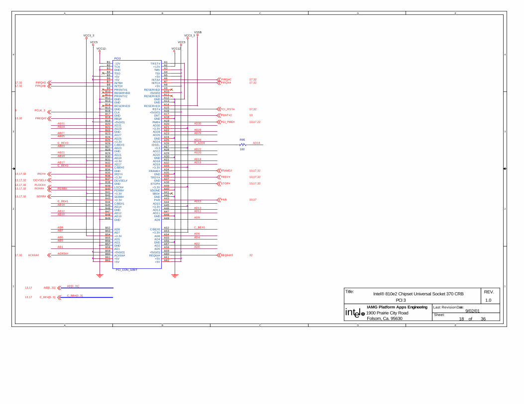
A
A
B
B
C
C
D
D
E
E
4 4
3 3
2 2
1 1
Intel® 810e2 Chipset Universal Socket 370 CRBPCI 3
36
1.0
9/02/01
18
IAMG Platform Apps Engineering1900 Prairie City RoadFolsom, Ca. 95630
REV.
R
Last Revision Date:
Sheet:of
Title:
intel
AD22AD20
AD18AD16
AD15
AD9
AD6AD4
AD2AD0
AD31AD29
AD27AD25
AD23
AD21AD19
AD17
PERR#
AD14
AD12AD10
AD8AD7
AD5AD3
AD1
ACK64#
C_BE#3
C_BE#2
C_BE#1
AD18
C_BE#0
AD30
R_AD18AD24
AD11AD13
AD28AD26
AD[0..31]
C_BE#[0..3]
PIRQ#B17,32
PCLK_36
IRDY#13,17,32
DEVSEL#13,17,32
SERR#13,17,32
AD[0..31]13,17
C_BE#[0..3]13,17
PIRQ#C 17,32PIRQ#A 17,32
PGNT#2 13
PCI_PME# 13,17,22
FRAME# 13,17,32
TRDY# 13,17,32
STOP# 13,17,32
PAR 13,17
ACK64#17,32
PCI_RST# 17,32
PREQ#213,32
PIRQ#D17,32
PERR#13,17,32PLOCK#13,17,32
REQ64#3 32
VCC3_3
VCC5
VCC12VCC12-
VCC5
VCC3_3V3SB
PCI3
PCI_CON_32BIT
A1A2A3A4A5A6A7A8A9A10A11A12A13A14A15A16A17A18A19A20A21A22A23A24A25A26A27A28A29A30A31A32A33A34A35A36A37A38A39A40A41A42A43A44A45A46A47A48A49
A52A53A54A55A56A57A58A59A60A61A62
B1B2B3B4B5B6B7B8B9
B10B11B12B13B14B15B16B17B18B19B20B21B22B23B24B25B26B27B28B29B30B31B32B33B34B35B36B37B38B39B40B41B42B43B44B45B46B47B48B49
B52B53B54B55B56B57B58B59B60B61B62
TRST#+12VTMSTDI+5V
INTA#INTC#
+5VRESERVED
+5V(I/O)RESERVED
GNDGND
RESERVEDRST#
+5V(I/O)GNTGND
PME#AD30+3.3VAD28AD26GND
AD24IDSEL
+3.3AD22AD20GND
AD18AD16+3.3V
FRAME#GND
TRDY#GND
STOP#+3.3V
SDONESBO#
GNDPAR
AD15+3.3VAD13AD11GNDAD9
C/BE#0+3.3V
AD6AD4GNDAD2AD0
+5V(I/O)REQ64#
+5V+5V
-12VTCKGNDTDO+5V+5VINTB#INTD#PRSNT#1RESERVEDPRSNT#2GNDGNDRESERVEDGNDCLKGNDREQ#+5V(I/O)AD31AD29GNDAD27AD25+3.3VC/BE#3AD23GNDAD21AD19+3.3VAD17C/BE#2GNDIRDY#+3.3VDEVSEL#GNDLOCK#PERR#+3.3VSERR#+3.3VC/BE#1AD14GNDAD12AD10GND
AD8AD7+3.3VAD5AD3GNDAD1+5V(I/O)ACK64#+5V+5V
R95
100
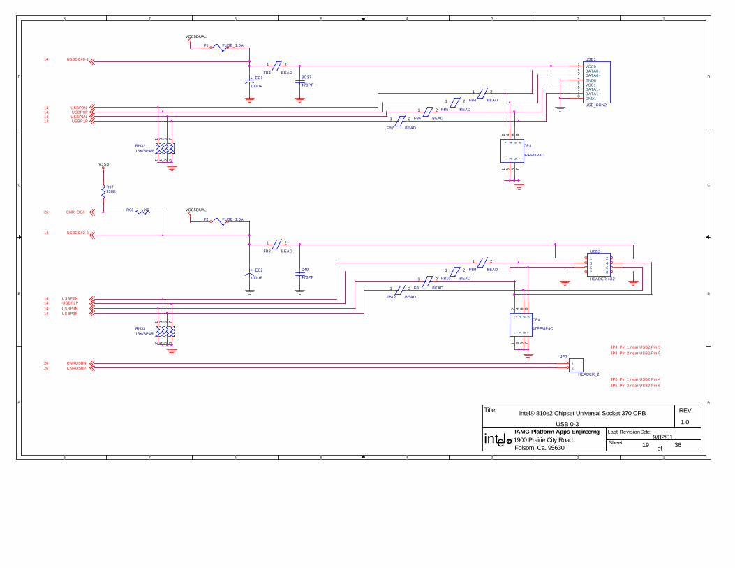
8
8
7
7
6
6
5
5
4
4
3
3
2
2
1
1
D D
C C
B B
A A
JP4 Pin 1 near USB2 Pin 3
JP4 Pin 2 near USB2 Pin 5
JP5 Pin 1 near USB2 Pin 4
JP5 Pin 2 near USB2 Pin 6
Intel® 810e2 Chipset Universal Socket 370 CRB
USB 0-3
36
1.0
9/02/0119
IAMG Platform Apps Engineering1900 Prairie City RoadFolsom, Ca. 95630
REV.
R
Last Revision Date:
Sheet:of
Title:
intel
USBP0P14USBP1N14USBP1P14
USBP0N14
USBOC#0-114
USBP3N14
USBOC#2-314
CNR_OC#26
USBP2P14
USBP3P14
USBP2N14
CNRUSBN26CNRUSBP26
VCC5DUAL
VCC5DUAL
V3SB
RN3315K/8P4R
1 3 5 7
2 4 6 8
FB10 BEAD
1 2
CP4
47PF/8P4C
1 3 5 782 4 6
1 3 5 782 4 6
JP7
HEADER_2
12
FB4 BEAD
1 2
+ EC2
100UF
FB7 BEAD
1 2
+ EC1
100UF
FB3 BEAD
1 2
F2 FUSE_1.0A
FB6 BEAD
1 2
USB1
USB_CON2
12345678
VCC0DATA0-DATA0+GND0VCC1DATA1-DATA1+GND1
FB8 BEAD
1 2
USB2
HEADER 4X2
1 23 45 67 8
FB5 BEAD
1 2
R98 X0
R97330K
FB12 BEAD
1 2
FB9 BEAD
1 2
C49
470PF
RN3215K/8P4R
1 3 5 7
2 4 6 8
CP3
47PF/8P4C
1 3 5 782 4 6
1 3 5 782 4 6
FB11 BEAD
1 2
BC37
470PF
F1 FUSE_1.0A

A
A
A A
AC'97CODEC
"SINGLE POINT CONNECTION"
Intel® 810e2 Chipset Universal Socket 370 CRB
AC97 CODEC
36
1.0
9/02/01
20
IAMG Platform Apps Engineering1900 Prairie City RoadFolsom, Ca. 95630
REV.
R
Last Revision Date:
Sheet:of
Title:
intel
AC97SPKR26 EAPD 21
AUD_VREFOUT 21
AC_SYNC 14,26AC_BITCLK 14,26
AC_SDIN0 14,26,32
PRI_DWN_RST# 31AC_SDOUT 14,26,31
LINE_IN_L21
LNLVL_OUT_R21
CD_R21
CD_REF21
MIC_IN21
LINE_IN_R21
CD_L21
LNLVL_OUT_L21
AUX_R21AUX_L21
VCC3_3 VCC5 VCC5_AUDIO
MC6
0.1UF
BC41
0.1UF
R100
1K
MC5 X1UF
C51
2700PF
U10
CS4299
4 1 7 9 38 42 25 26 40 44 43
122423212220181917161415133736354139
29 30 32 31 33 34 27 28 3 2
1158106
46454847
DV
SS
1
DV
DD
1
DV
SS
2
DV
DD
2
AV
DD
2
AV
SS
2
AV
DD
1
AV
SS
1
NC
40N
C44
NC
43
PC_BEEPLINE_IN_RLINE_IN_LMIC1MIC2CD_RCD_LCD_REFVIDEO_RVIDEO_LAUX_LAUX_RPHONEMONO_OUTLINE_OUT_RLINE_OUT_LLNLVL_OUT_RLNLVL_OUT_L
AF
ILT
1
AF
ILT
2
FILT
_L
FILT
_R
RX
3D
CX
3D
VR
EF
VR
EFO
UT
XTL
_OU
T
XT
L_IN
RESET#SDATA_OUT
SDATA_INSYNC
BIT_CLK
CS1CS0
CHAIN_CLKEAPD
BC39
0.1UF
R101 X0
C52
2700PF
BC40
0.1UF
BC38
0.1UF
MC7
1UF
MC8
1UF
R1031K
C50
10PF
Y3
24.576MHZ
R99 10K
MC9
0.1UF
BC42
0.1UFMC12
2.2UF
C54
22PF
PFB1
BEAD
12
MC10
0.1UF
MC11
4.7UF
C53
22PF
R102
1K
MC4 1UF

8
8
7
7
6
6
5
5
4
4
3
3
2
2
1
1
D D
C C
B B
A A
CD Analog InputLine_In Analog Input
Microphone Input
Stereo HP/Spkr out
"SINGLE POINT CONNECTION"Intel® 810e2 Chipset Universal Socket 370 CRB
Audio I/O
36
1.0
9/02/01
21
IAMG Platform Apps Engineering1900 Prairie City RoadFolsom, Ca. 95630
REV.
R
Last Revision Date:
Sheet:of
Title:
intel
CD_ING
AUX_INL
AUX_INR
CD_INR
CD_INL
LNLVL_OUT_R20
AUD_VREFOUT20
LINE_IN_R20
LINE_IN_L20
CD_R 20
CD_L 20
CD_REF 20
MIC_IN20
AUX_L 20
AUX_R 20
LNLVL_OUT_L20
EAPD20
VCC5_AUDIO
AUX1
2.54_WAFER_4
1
32
4
MC19
1UF
CD2
2mm_WAFER_4
1
32
4
C65
100PF
MC18
1UF
MC21
1UFFB17
BEAD
1 2
R118
2.2K
JK1
PHONEJACK
R105
20
R109
20K
U11
LM4880
1234
8765
OUTAINABYPASSGND
VDDOUTB
INBSHUTDN
MC13
1UF
C67
100PF
R115220K
C62
100PF
MC23
1UF
FB15
BEAD
1 2
C660.01UF
MC20
1UF
R113
1K
R107 20K
JK2
PHONEJACK
MC16
1UF
R10820K
R119
1K
R1101K
C58
100PF
+
C56
100UF
+
C55
100UF
MC17
1UF
FB13
BEAD
1 2
R117220K
R116220K
C68
100PF
FB16
BEAD
1 2
C63
100PF
R114
1K
CD1
2.54_WAFER_4
1
32
4
C59 100PF
MC14
1UF
MC22
1UF
C61
100PF
JK3
PHONEJACK
R1121K
C57
100PF
R104
20
R106
20K
MC151UF
R111
1K
BC43
0.1UF
C69
100PF
FB14
BEAD
1 2
C60100PF
C64
100PF

A
A
B
B
C
C
D
D
E
E
4 4
3 3
2 2
1 1
Parallel Port
WAKE ON MODEM
COM1
COM2
WAKE ON LAN
Intel® 810e2 Chipset Universal Socket 370 CRB
WOL, WOR & 2S1P
36
1.0
9/02/01
22
IAMG Platform Apps Engineering1900 Prairie City RoadFolsom, Ca. 95630
REV.
R
Last Revision Date:
Sheet:of
Title:
intel
RI0
RI1
DCD0DTR0CTS0TXDD0RTS0RXDD0DSR0RI0
DCD1DTR1CTS1TXDD1RTS1RXDD1DSR1RI1
DSR0RXDD0
RXDD1
TXDD1DCD1
RTS1
DTR1
DTR0
TXDD0RTS0
CTS0
DCD0
RI1
RI0
CTS1DSR1
DCD#016DTR#016CTS#016
TXD016RTS#016
DSR#016RI#016
DCD#116DTR#116CTS#116
TXD116RTS#116
DSR#116RI#116
RXD016
RXD116
PDR716
PDR116
STB#16
PDR016
PDR316
PDR416
PDR516
PAR_INIT#16
SLIN#16
ACK#16
BUSY16
PE16
SLCT16
ERR#16
PDR216
PDR616
AFD#16
PCI_PME#13,17,18
ICH_RI#14,32
VCC5
VCC12- VCC12 VCC5
VCC5SBY
R1252.2K
CN3
100PF/8P4C
1 3 5 782 4 6
1 3 5 782 4 6
WOL1
HEADER_3*1(2MM)
1
32R120
100
D4
SS12/SMD
CN2
100PF/8P4C
1 3 5 782 4 6
1 3 5 782 4 6
R122
10K
D5
SS12/SMD
COM2
HEADER_5X2
13579
2468
10
R124
10K
Q22N3904
U12
GD75232
2345678
1
19181716151413
9
1011
12
20
RA1RA2RA3DY1DY2RA4DY3
12V
RY1RY2RY3DA1DA2RY4DA3
RA5
-12VGND
RY5
5V
CN1
100PF/8P4C
1 3 5 782 4 6
1 3 5 782 4 6
BC46.1U
COM1
CONNECTOR_DB9
594837261
Q32N3904
U14
PAC-S1284
1
2
3 26
4
5
6
7
8
9
10
11
12
13
14
28
27
15
25
24
23
22
21
20
19
18
17
16
P1
P2
SI1 SO1
SI2
SI3
SI4
SI5
P3
SI6
P4
SI7
P5
SI8
SI9
P8
P7
P6
SO2
SO3
SO4
GND
SO5
VCC
SO6
SO7
SO8
SO9
CN4
100PF/8P4C
1 3 5 782 4 6
1 3 5 782 4 6
R1232.2K
BC44.1U
LPT1
LPT
1325122411231022
921
820
719
618
517
416
315
214
1
Q1
2N3904
U13
GD75232
2345678
1
19181716151413
9
1011
12
20
RA1RA2RA3DY1DY2RA4DY3
12V
RY1RY2RY3DA1DA2RY4DA3
RA5
-12VGND
RY5
5V
R1214.7K
BC45.1U
D6
SS12/SMD

A
A
B
B
C
C
D
D
E
E
4 4
3 3
2 2
1 1
Game Port
KeyboardMouse
IRIntel® 810e2 Chipset Universal Socket 370 CRB
Kybrd / Mse / F. Disk / Gme Connectors
36
1.0
9/02/01
23
IAMG Platform Apps Engineering1900 Prairie City RoadFolsom, Ca. 95630
REV.
R
Last Revision Date:
Sheet:of
Title:
intel
MIDI_OUTPUT
JOY_1YJ2BUT2
JOY_2Y
MIDI_INPUTJ1BUT2
JOY_2XJOY_1XJ2BUT1J1BUT1
JOY2X16
J2BUTTON216
MIDI_OUT16
J1BUTTON116
J1BUTTON216
JOY1X16
JOY1Y16JOY2Y16
J2BUTTON116
MIDI_IN16
KDAT16
KCLK16
MDAT16
MCLK16
IRRX16
IRTX16
VCC5VCC5 VCC5VCC5 VCC5VCC5 VCC5
VCC5
VCC5DUAL
RN34 1K/8P4R
1357
2468
FB23
BEAD
1 2
R128
4.7K
R1324.7K
R126 0
FB18
BEAD
12
CN7
470PF8P4C
13578
246
13578
246
FB20
BEAD
1 2
C83
2.2UF
C711000PF
C77
470PF
C70
470PF
F3 XFUSE_1.0A
R134 47
C7522PF
C8022PF
FB24
BEAD
1 2
FB21
BEAD
1 2
R1304.7K
RN35 1K/8P4R
1357
2468
IR1
HEADER_1X5
1
32
45
C7822PF
U15
KB/MOUSE
123456
131415
1617
789101112
C76
470PF
R136 0
RN36 4.7K/8P4R
1357
2468
F4 XFUSE_1.0A
C73
470PF
J4
GAME_PORT
815
714
613
512
411
310
291
C791000PF
FB22
BEAD
1 2
R127
4.7K
CN6
470PF/8P4C
13578 246
13578 246
C7222PF
C811000PF
FB19
BEAD
1 2
C82
2.2UF
R133 47
R135 0
R1294.7K
F5 XFUSE_1.0A
CN5
470PF/8P4C
13578 246
13578 246
C741000PF
R1314.7K

A
A
A A
Do Not Stuff
Digital Video Out
Place C106Anear U8A pin 3
Intel® 810e2 Chipset Universal Socket 370 CRBDigital Video Out
36
1.0
9/02/01
24
IAMG Platform Apps Engineering1900 Prairie City RoadFolsom, Ca. 95630
REV.
Last Revision Date:
Sheet:of
Title:
intel
FTD9
EX
TR
S_P
U
A3_PD
TEST_PD
FPP1V3
A1_PD
FP
DV
3
A2_PD
FTD11
FPAV3
FTD10
FTVREF
FTD8
FTD1
FTD7
FTD0
FTD6
FTD2
FTD4
FTD5
FTD3
FP
DV
3
SL_STALL 9
FTCLK09FTCLK19
FTBLNK#9FTHSYNC9
FTVSYNC9
FTD[11:0]9
TX2+ 25
3VFTSCL 9,25
TX0+ 25
PCIRST# 7,15,16,32
TX0- 25
TX2- 25
3VHTPLG 25
3VFTSDA 9,25
TX1- 25
TX1+ 25
TXC+ 25TXC- 25
VCC1_8
VCC3_3
VCC3_3
VCC3_3
R141A
1 K
+10
UF
C90
A1
2
0.01
UF
C95
A
L10A
12
L 9 A
12
R143A
1 K
+10
0pF
C94
A
12
+10
UF
C92
A1
2
L 8 A
12
R142A
4.7K
100P
F
C85
A
100P
F
C93
A
100P
F
C91
A
R 137A
1K
100P
F
C89
A
R 139A
1K
10
0PF
C87
A
10
0PF
C88
A
Flat PanelTransmitter
DFP
U16A
17202632
2329
7
63
62
51
50
47
46
45
42
61
39
38
37
36
60
59
58
55
54
53
52
2
164864
4
57
56
184925
24
28
27
31
30
22
21
112333
5
41
40
43
44
6
8
13
11
10
9
15
14
34
35
19
PGN
D
AGN
D0
AGN
D1
AGN
D2
AVC
C0
AVC
C1
CTL2/A2/DK2
D0
D1
D10
D11
D12
D13
D14
D17
D2
D20
D21
D22
D23
D3
D4
D5
D6
D7
D8
D9
D E
GN
D0
GN
D1
GN
D2
H S
IDCLK+
IDCLK-
PVC
C0
PVC
C1
TX0+
TX0-
TX1+
TX1-
TX2+
TX2-
TXC+
TXC-
VCC0
VCC1
VCC2
VREF
VS
D18
D19
D16/PFEN
D15
CTL3/A3/DK3
CTL1/A1/DK1
ISEL/RST
MSEN
PD
EDGE/CHG
BSEL/SCL
DSEL/SDA
TEST
DKEN
EXT_RS
+
10U
F
C84
A
12
R140A
1 K
100P
F
C86
AR 138A400
1 %

A
A
A A
Protection Circuit
for 20V Tolerance
20 Pin Flat Panel Connector
is also populated.Populate if DFP Device
De-BounceCircuit
BLM11B750S is rated a t70Ohms at 100MHz
Video Connectors
Do Not Populate
5V to 3.3V Translation / Isolation
Place R66A,R67A,&R69A Close to VGAConnector
VGA Connector
Do Not Stuff C114A and C115A
Do Not Stuff C117A and C118A
Intel® 810e2 Chipset Universal Socke t 370 CRB
Video Connectors
36
1.0
9/02/01
25
IAMG Platform Apps Engineering1900 Prairie City RoadFolsom, Ca. 95630
REV.
Last Revision Date:
Sheet:of
Title:
intel
5VHSYNC
5VHSYNC
5VHTPL G
5VVSYNC
5VFTSC L
5VFTSDA
CO
N_F
TSC
L
CO
N_F
TSD
A
QSSDA
QSSCL
L_VSYNC
L_BLUE
L_HSYNC
5VDDCDA
L_RED
FUSE_5
MON2PU
MONOPU
QS4_3V
5VDDCDA
5VFTSDA
L_GREEN
5VDDCCL
5VVSYNC
CR
T5V_F
5VDDCCL
5VFTSCL
CON_HTPLG 5VHTPLG
TX2+ 24
TX2- 24
TX0+ 24
TX0- 24
SMBDATA 11,12,14,16,26,32SMBCLK 11,12,14,16,26,32
TX1+24TX1-24
TXC+24TXC-24
3VDDCDA93VDDCCL9
CRT_HSYNC9CRT_VSYNC9
3VHTPLG24
3VFTSDA9,243VFTSCL9,24
CK_SMBDATA6CK_SMBCLK6
VID_RED9
VID_GREEN9
VID_BLUE9
VCC5 VCC5
VCC5
VCC5
VCC5
VCC5
VCC1_8
VCC1_8
VCC1_8
L12A
12
3.3P
F
C10
2A
10P
F
C10
9A
C R 5 A
AC
3.3P
F
C10
1A
BAT54S
C R 1 A
3
2
1
L14A
BLM11B750S
1 2
10P
F
C11
0A
R 153A
4.7K
R158A
2.2K
3.3P
F
C10
0A
RP5A
2.2K
1 2 3 45678
3.3P
F
C97
A
BAT54S
C R 7 A
3
2
1
BAT54S
C R 3 A
3
2
1
R154A
0K
R149A751%
R159A
2.2K
0.1U
F
C10
4A
10P
F
C10
8A
3.3P
F
C11
1A
L11A
BLM11B750S
1 2
3.3P
F
C10
6A
R157A
0 K
R150A
0 K
2.5A
F6A
12
R145A1K
R152A
0K
15510
6111
J6A
7
6
1
11
2
12
8
3
13
9
4
14
10
5
15
R146A751%
0.01
UF
C98
A
10P
F
C10
7A
J5A
15
6 16
7 17
8 18
9 19
10 20
2 12
3
4 14
5
111
13
L13A
BLM11B750S
1 2
3.3P
F
C10
3A
R144A1K
3.3P
F
C11
2A
QST3384U17A
1
23
20
16
15
1011
98
6
3
4 5
18 19
13
2
22
24
14
17
21
7
12BEA#
2B5
2B4
2B2
2B1
1B51A5
1B41A4
1B3
1A1
1A2 1B2
2A3 2B3
BEB#
1B1
2A5
VCC
2A1
2A2
2A4
1A3
G N D
3.3P
F
C10
5A
R156A
0 K
R151A
0 K
+
10U
F
C99
A1
2
R147A
2.2K
BAT54S
C R 6 A
3
2
1
BAT54S
C R 4 A
3
2
1
1N5821
C R 2 A -
+
AC
3.3P
F
C96
A
R155A751%
R148
30k
12

8
8
7
7
6
6
5
5
4
4
3
3
2
2
1
1
D D
C C
B B
A A
HDD LED
PWR_SW
KEYLOCK
SMI_SW
SPEAKER
RESET
GREEN LED
RESERVE
TRADITIONAL PC SOUND
3-4 ON1-2 ON
MIXED IN ON_BOARD AC97 CODEC
JP2ON BOARD BUZZ OR DIRECT TO SPKR
Intel® 810e2 Chipset Universal Socket 370 CRB
Front Panel & CNR
36
1.0
9/02/01
26
IAMG Platform Apps Engineering1900 Prairie City RoadFolsom, Ca. 95630
REV.
R
Last Revision Date:
Sheet:of
Title:
intel
SMBDATA
SMBCLK
IDEACTS#15
BEEP16
KEYLOCK#16
PANSWIN16
IDEACTP#15
HWRST#27
SUSLED16
EXTSMI#13
ICH_SPKR14,31
AC97SPKR20
AC_SDIN1 14,32AC_SDIN0 14,20,32
AC_RST# 14,31
CNR_OC#19
AC_SDOUT14,20,31AC_SYNC14,20
AC_BITCLK14,20
PRI_DWN31SMBCLK11,12,14,16,25,32 SMBDATA 11,12,14,16,25,32
CNRUSBN 19
CNRUSBP 19
EE_CS 14
LAN_TXD0 13LAN_TXD2 13
LAN_CLK 13LAN_RXD1 13
LAN_RXD013
LAN_TXD113LAN_RSTSYNC13
LAN_RXD213
EE_SHCLK14EE_DOUT 14EE_DIN14
VCC5
VCC5SBY VCC5
VCC5
VCC5
V3SB
VCC5
VCC12VCC5SBYVCC12- VCC5V3SB
VCC5SBY
VCC3_3
VCC5SBY
VCC5VCC5
R162220
SMB1
SMBCON
1
32
45
C113
47PF
R16810K
R17010K
Q42N3904
R16310K
BC480.1UF
BC47
0.1UF
R17610K
PN2
HEADER_14
1234567891011121314
R177 68
R16715K
R174 330
PN1
HEADER_14
1234567891011121314
JP8
XHEADER 2X2
1 23 4
D9
LED
Q52N3904
R175
33
CNRSLOT1
CNR
B1B2B3B4B5B6B7B8B9
B10B11B12B13B14B15B16B17B18B19
B20B21B22B23B24B25B26B27B28B29B30
A1A2A3A4A5A6A7A8A9A10A11A12A13A14A15A16A17A18A19
A20A21A22A23A24A25A26A27A28A29A30
RESERVEDRESERVEDRESERVEDGNDRESERVEDRESERVEDGNDLAN_TXD1LAN_RSTSYNCGNDLAN_RXD2LAN_RXD0GNDRESERVED+5VDUALUSB_OC#GND-12V+3.3VD
GNDEE_DOUTEE_SHCLKGNDSMB_A0SMB_SCLPRIMARY_DN#GNDAC97_SYNCAC97_SD_OUTAC97_BITCLK
RESERVEDRESERVED
GNDRESERVEDRESERVED
GNDLAN_TXD2LAN_TXD0
GNDLAN_CLK
LAN_RXD1RESERVED
USB+GND
USB-+12VGND
+3.3VDUAL+5VD
GNDEE_DINEE_CS
SMB_A1SMB_A2
SMB_SDAAC97_RESET#
RESERVEDAC97_SD_IN1AC97_SD_IN0
GND
R165220
D7 1N4148
R180 0
R178 68
R172150
C114
47PF
R164150
R16110K
R179 2.2K
SMB2
SMBCON
1
32
45
R173
0
Q62N3904
SP1
BUZZER
R1602.2K
D8 1N4148
R16615K
R1690
C115
0.1UF
R17110K

A
A
B
B
C
C
D
D
E
E
4 4
3 3
2 2
1 1
Resume Reset Circuitry. 22msec delay
Intel® 810e2 Chipset Universal Socket 370 CRB
ATX Power
36
1.0
9/02/01
27
IAMG Platform Apps Engineering1900 Prairie City RoadFolsom, Ca. 95630
REV.
R
Last Revision Date:
Sheet:of
Title:
intel
ATXPWROK
HWRST#26
PS_ON16
DBRESET#4
PWROK 14,16
RSMRST# 14,16
VCC12-
VCC_5-
VCC5VCC12
VCC3_3 VCC5VCC5SBY
VCC5SBY
VCC5SBY
V3SB VCC5SBY
V3SBV3SB
VCC5SBY
V3SB
VCC5SBY
V3SBV3SB V3SB
VCC3_3SB
C11910uF
12
BC49.1U
JP9
Place JP near front panel hdr
BC50.1U
C118
0.01uF
R
100K
C116
2UF
RA
10K
U19C
74LVC14A
65
U18B
74LVC06A
3 4
R18333K
D101N4148
U18C
74LVC06A
5 6
R18115K
R186A
22
U21A
74LVC14A
1 2
714
ATXPR1
ATX_PWCON
2345678910
11121314151617181920
1
3.3VGND+5V
GND+5V
GNDPWROKAUX5V
+12V
3.3V-12VGNDPS_ONGNDGNDGND-5V+5V+5V
3.3V
R1851K
U19A
74LVC14A
714
21
BC51
1.0uF
U20A74LS132
1
23
714
A
BY
GN
DV
CC
R184 100
R182
4.7K
SW1
Reset button
1 2
U21B
74LVC14A
3 4
714
U18D
74LVC06A
9 8
U18A
74LVC06A
1 2
714
R187A
22k
C117
1.0uF
U19B
74LVC14A
43

A
A
B
B
C
C
D
D
E
E
4 4
3 3
2 2
1 1
CPU FAN
CHASSIS FAN
PWR FAN
Temperature Sensing
If case is opened,this switch should be closed.
Voltage Sensing
"power use"
"system use"
Intel® 810e2 Chipset Universal Socket 370 CRB
H/W Monitor
36
1.0
9/02/01
28
IAMG Platform Apps Engineering1900 Prairie City RoadFolsom, Ca. 95630
REV.
R
Last Revision Date:
Sheet:of
Title:
intel
+12CHFAN
+12CPUFAN
FANIO1 16FANPWM116
FANIO2 16FANPWM216
FANIO3 16
HM_VREF16
THRMDN4,16
VTIN116
VTIN24,16
+3.3VIN 16
-5VIN 16
+12VIN 16
VCORE 16
-12VIN 16
VTT 16
VTIN316
CASEOPEN#14,16
VCC12
VCCVID
VCC12-
VCC_5-
VTT1_5
VCC12
VCC3_3
VCC12
VCC12
VCC5
VCC5
VCC5
VCCRTC
JP10
HEADER_21 2
R201 10M
FAN3
HEADER_3
1
32
R198
10K
PR13
232K,1%
PR10
28K,1%
D12
1N4148
+EC4
22UF
FAN2
HEADER_3
1
32
R191
1K
R196 1K
+EC3
22UF
Q72N2907
R192
30K
S1
HEADER_2PIN
R202
1K
R195
10K
R199
10K
R190 1K
tRT2
10K_1%-THRM/0603
PR8
10K,1%
PR9
10K,1%
tRT1
X10K_1%-THRM/0603
FAN1
HEADER_3
1
32
PR15
120K,1%
D13
1N4148
D11
1N4148Q8
2N7002
R200 510PR12
56K,1%
Q92N2907
C120
3300PF
+EC5
22UF
PR14
56K,1%
Q10
2N7002
R197
1K
R194
4.7K
R193 510
R189
4.7K
PR11
10K,1%
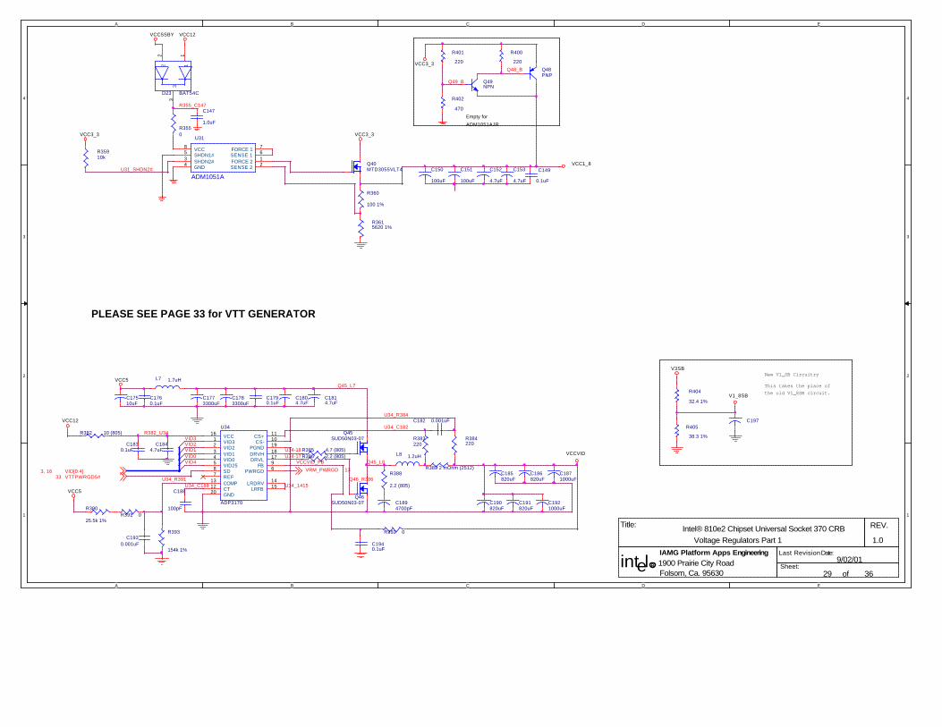
A
A
B
B
C
C
D
D
E
E
4 4
3 3
2 2
1 1
Empty for
ADM1051AJR
New V1_SB Circuitry
This takes the place ofthe old V1_8SB circuit.
PLEASE SEE PAGE 33 for VTT GENERATOR
Intel® 810e2 Chipset Universal Socket 370 CRBVoltage Regulators Part 1
36
1.0
9/02/01
29
IAMG Platform Apps Engineering1900 Prairie City RoadFolsom, Ca. 95630
REV.
R
Last Revision Date:
Sheet:of
Title:
intel
R355_C147
Q48_B
U31_SHDN2#
Q49_B
VID0Q45_L8
U34_R384
Q46_R386
R382_U34VID3
U34_C182
U34-18
VCCVID_FB
VID2
VID4
U34_R391
U34-17
U34_C188 U34_1415
VID1
Q45_L7
VID[0:4]3, 16 VRM_PWRGD 13VTTPWRGD5#33
VCC5SBY
VCC3_3
VCC3_3
VCC5
VCCVID
V1_8SB
VCC12
V3SB
VCC5
VCC1_8
VCC12
VCC3_3
C1773300uF
C149
0.1uF
R35910k
C1783300uF
R360
100 1%
C1790.1uF
R3615620 1%
C1804.7uF
C1814.7uF
R385 4.7 (805)
R390
25.5k 1%R391 0
U34
ADP3170
161
432
5
181796
20
1415
13
8
12
111019
7
VCCVID3
VID0VID1VID2
VID25
DRVHDRVL
FBPWRGD
GND
LRDRVLRFB
COMP
SD
CT
CS+CS-
PGND
REF
R393
154k 1%
C185820uF
R404
32.4 1%
C190820uF
R405
38.3 1%
R386 2.2 (805)
R382 10 (805)
C186820uF
C191820uF
C1940.1uF
R401
220
C1921000uF
C1930.001uF
R400
220
R388
2.2 (805)
C1871000uF
R389 2 mOhm (2512)
R383220
C1894700pF
R384220
L7 1.7uH
Q45SUD50N03-07
R3550
Q46SUD50N03-07
ADM1051A
U31
8
4
53
7
16
2
VCC
GND
SHDN1#SHDN2#
FORCE 1
FORCE 2SENSE 1
SENSE 2
C197
Q40MTD3055VLT4
R392 0
Q49NPN
C182 0.001uF
C147
1.0uF
Q48PNP
L8 1.2uH
C1830.1uF
R402
470
C150
100uF
D23 BAT54C
12
3
12
3C151
100uF
C1844.7uF
C152
4.7uF
C153
4.7uF
C17510uF
C188
100pF
C1760.1uF

A
A
B
B
C
C
D
D
E
E
4 4
3 3
2 2
1 1
Intel® 810e2 Chipset Universal Socket 370 CRBVoltage Regulators Part 2
36
1.0
9/02/01
30
IAMG Platform Apps Engineering1900 Prairie City RoadFolsom, Ca. 95630
REV.
R
Last Revision Date:
Sheet:of
Title:
intel
SLP_S5#14SLP_S3#6,14,16
VCC3_3VCC12VCC5SBY
VCC3SBYV3SB VCC5SBY
VCC5DUALVCC5SBY
VCC5 VCC2_5
VCC3_3
VCC5
V1_8SBV3SB
C132
1UF
Q17
HUF76121D3S/TO252
PR16
100,1%
+EC25
100UF
Q16
LM1117ADJ
3
1
2VIN AD
J
VOUT
+ EC31
10UFPR18
120,1%
PR17
100,1%
+EC30
100UFQ19NDS356AP/SOT23
R21910K
+ EC32
10UF
+ EC27
100UF
+EC34
100UF
+EC23
100UF
C134
0.1UF
C130
0.1UF
Q20
LM1117ADJ
3
1
2VIN AD
J
VOUT
+EC33
100UF
+EC24
10UF
Q18
NZT651/SOT223
C131
1UF
+EC28
1500UF
C133
1UF
PR19
60,1%
Q21
FDS8936 / SI9936
1
2
3
4 5
6
7
8S1
G1
S2
G2 D2
D2
D1
D1
+EC29
10UF
U23
HIP6501
141
3
49
6752
13
15
16
11
10
12
812
V
5VS
B
3V3DLSB
3V3DLFAULT/MSET
S3S5EN5VDLEN3VDLSS
DRV2
VSEN2
5VDLSB
DLA
5VDL
GN
D
+ EC26
10UF

A
A
B
B
C
C
D
D
E
E
4 4
3 3
2 2
1 1
SW1:5
OFF FORCE CPU FREQ STRAP TO SAFE MODE(1111)USE CPU FREQ STRAP IN ICH REGISTER
AC_SDOUTON
STRAP(SPKR)
OFF REBOOT ON 2ND WATCHDOG TIMEOUT
SW1:6NO REBOOT ON 2ND WATCHDOG TIMEOUT
SW1:1-2
ON
ON 8
SW1:7-8ON 7
ON BOARD AC97 CODECPRIMARY CODECDISABLE
ON1-2 CPU DEFAULTOFF 1-2BY SW2:3-4
SW1:3-4FSB / SYSTEM MEMORY
FSB / SYSTEM MEMORY
OFF OFF
ON ONOFF ON
66M/PC100100M/PC100133M/PC100 OR PC133
Intel® 810e2 Chipset Universal Socket 370 CRBSystem Configuration
36
1.0
9/02/01
31
IAMG Platform Apps Engineering1900 Prairie City RoadFolsom, Ca. 95630
REV.
R
Last Revision Date:
Sheet:of
Title:
intel
R_REFCLK 9
AC_SDOUT 14,20,26
AC_RST#14,26
FMOD1 6
BSEL#14
PRI_DWN26
BSEL#04
ICH_SPKR 14,26
PRI_DWN_RST# 20
FREQSEL 6,9
VCC3_3
R225 8.2K
D15
1N4148
SW2 DIPSW-812345678
161514131211109
JUMPERJP?
R2211.8K
R223 10K
R2221.8K
R224
8.2K

A
A
B
B
C
C
D
D
E
E
4 4
3 3
2 2
1 1
PCI ICH
Do not populate
CPU
Intel® 810e2 Chipset Universal Socket 370 CRBPullup Resistors
36
1.0
9/02/01
32
IAMG Platform Apps Engineering1900 Prairie City RoadFolsom, Ca. 95630
REV.
R
Last Revision Date:
Sheet:of
Title:
intel
SERR#13,17,18PLOCK#13,17,18STOP#13,17,18DEVSEL#13,17,18
IRDY#13,17,18FRAME#13,17,18
PERR#13,17,18
TRDY#13,17,18
PREQ#113,17PREQ#013,17
PREQ#213,18
ACK64#17,18
SMBALERT#14
KBRST#13,16A20GATE13,16
PCI_REQ#A13OVT#14,16
AC_SDIN114,26
AC_SDIN014,20,26
ICH_IRQ#C13
ICH_IRQ#G13
ICH_IRQ#D13
ICH_IRQ#F13
ICH_IRQ#A13ICH_IRQ#B13
ICH_IRQ#H13
ICH_IRQ#E13
PIRQ#C17,18PIRQ#B17,18
PIRQ#D17,18
PIRQ#A17,18
SMLINK114,18SMLINK014,18
SERIRQ13,16
GPIO2813GPIO2713GPIO2514GPI813
REQ64#117REQ64#217REQ64#318
ICHRST#13PCIRST# 7,15,16,24
PCI_RST# 17,18
IDERST# 15
SMBDATA11,12,14,16,25,26
LPC_PME#13,16
SMBCLK11,12,14,16,25,26
PREQ#413
PREQ#313,18PREQ#513
REQ64#418
ICH_RI#14,22
APICD14,13
APICD04,13
FERR#4,13
VCC5 V3SB
VCC3_3
V3SB
VCC3_3
VCC3_3
V3SB
VCC3_3
VCC3_3
VCC3_3
VCC3_3 VCC3_3
VCC3_3 VCC5
VCC3_3
VCC3_3
VCC3_3
VCC3_3VCC5SBY
VCC5SBY
V3SB
VCMOS
U24B
74LVC07A
3 4
147
U18F
74LVC06A
13 12
RN45
8.2k
1357
2468
R232 10K
U19D
74LVC14A
89
RN38
4.7K/8P4R
1357
2468
U24F
74LVC07A
13 12
147
R2261K
U24A
74LVC07A
1 2
147
R228 8.2K
R231 10K
R234A
150
RN42
8.2K/8P4R
1357
2468
BC52.1U
RN41
2.7K/8P4R
1357
2468
U24D
74LVC07A
9 8
147
RN37
4.7K/8P4R
1357
2468
U24E
74LVC07A
11 10
147
R2291K
RN44
0/8P4R
1357
2468
R233 8.2K
U19E
74LVC14A
1011
U18E
74LVC06A
11 10
RN39
2.7K/8P4R
1357
2468
R2301K
U24C
74LVC07A
5 6
147
RP6
2.7K/10P8R
12346789
10
5R1R2R3R4R5R6R7R8
C
C
RN46
X0/8P4R
1357
2468
RN43
2.7K/8P4R
1357
2468
R2271K
RN40
8.2K/8P4R
1357
2468
R235A
150R236
150
RN47
8.2k
1357
2468

5
5
4
4
3
3
2
2
1
1
D D
C C
B B
A A
Stuff either R5 or R415 see p4
No stuff C198 debug site only
0
2.0ms delaynominal
ASSERTED LOW!
3
jumper before removingR375
Debug only! Do NOT place
4, 13
4, 6
Intel® 810e2 Chipset Universal Socket 370 CRBUMB Circuits
36
1.0
9/02/01
33
IAMG Platform Apps Engineering1900 Prairie City RoadFolsom, Ca. 95630
REV.
R
Last Revision Date:
Sheet:of
Title:
intel
VR1_FB
U32-2
D24_U32
Q51_Q52
TUAL5#
TUAL5
ITPTCK 4
CPU_PWGD
TUAL54, 6
VTTPWRGD 3, 6
VTTPWRGD12 6
VTTPWRGD5# 29
THERMTRIP#4
PWRBTN# 14, 16
CPURST#4, 7
TUALDET
VTT
VCC5
VCC5
VCC5
VTTVCC3_3
VCC5
V1_8SB
VCC5
VCC5
V1_8SB
VTT
VCC12
V3SBVCC1_8
VCC1_8
R3681k 1%
Q432N7002
R408
0
C160
22uF Tantalum
R415
R3412.2K
Q502N3904
U32B
LM393 Ch2
5
67IN+ 2
IN- 2OUT 2
R41120K
R366732 1%
C1730.1 uF
Q262N3904
VR1
LT1587-ADJ
32
1
VINVOUT
ADJ
JP6JUMPER
R4094.7k
C17410 uF
R38020k
R3432.2K
Q522N3904
C162
0.1uF
Q252N7002
Q442N7002
R412 1K
R413510
Q41FDN335N
R3441k
Q512N3904
R367
10 1%
R375
0
U32A
LM393 Ch1
21
8
4
3
IN- 1OUT 1
VCC
GND
IN+ 1
R3811k
R4101K
R416
2.2K
R4141.3K
R364
49.9 1%
D24BAT54C
12
3
12
3
R3791k
C198X0.01uF
R3782.2k

5
5
4
4
3
3
2
2
1
1
D D
C C
B B
A A
Target 20ms afterVCC_CLOCK ispowered
Debug only - do
not stuff
Intel® 810e2 Chipset Universal Socket 370 CRBUMB Circuits
36
1.0
9/02/01
34
IAMG Platform Apps Engineering1900 Prairie City RoadFolsom, Ca. 95630
REV.
R
Last Revision Date:
Sheet:of
Title:
intel
ICH PWROK 14
PWROK16, 27
GMCH GTLREF 74 PROCESSOR GTLREF
VCC_CLOCKVCC3_3
VCC3_3
VTT
TUAL5
R475 ohm
R2150 ohm
R5150 ohm
Q1FDN335N
R377 0
D19
BAT54C
12
3
12
3
U33
741G08 AND
1
2
3
4
5
A
B GN
D
YVcc
R376 43k
C172
1.0uF
R1750 ohm
R375 ohm

A
A
A A
UNUSED GATES
Intel® 810e2 Chipset Universal Socket 370 CRBUnused Gates
36
1.0
9/02/01
35
IAMG Platform Apps Engineering1900 Prairie City RoadFolsom, Ca. 95630
REV.
Last Revision Date:
Sheet:of
Title:
intel
VCC5SBY
VCC3_3SBY
VCC3_3SBY
VCC3_3SBYVCC3_3SBYVCC3_3
U28C
SN74LVC07A
5 6
147
U 2 8 B
SN74LVC07A
3 4
147
U25C
SN74LVC06A
714
5 6
GN
DVC
C
A O
U 2 0 B
74LS132
4
56
714
A
BY
GN
DVC
C
SN74LVC07A
U 2 7 A
21
714
OA
GN
DVC
C
U 2 6 B
SN74LVC08A
147
64
5
U21C
74LVC14A
5 6
714
SN74LVC07A
U 2 7 B
43
714
OA
GN
DVC
C
U 2 5 A
SN74LVC06A
714
1 2
GN
DVC
C
A O
U 2 6 A
SN74LVC08A
147
31
2
SN74LVC07A
U27C
65
714
OA
GN
DVC
C
U21D
74LVC14A
9 8
714
U 2 5 B
SN74LVC06A
714
3 4
GN
DVC
C
A O
U 2 8 A
SN74LVC07A
1 2
147
U20C
74LS132
9
108
714
A
BY
GN
DVC
C
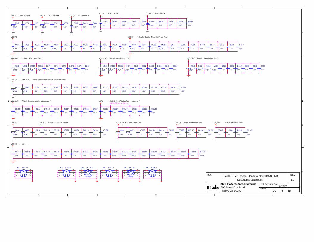
A
A
B
B
C
C
D
D
E
E
4 4
3 3
2 2
1 1
" GMCH : 0.1U//0.01U at each conner and each side-center "
" GMCH : Near Display Cache Quadrant "
" Display Cache : Near the Power Pins "
" GMCH : Near System Mem Quadrant "
" DIMM0 : Near Power Pins " " DIMM1 : Near Power Pins "
" ICH2 : 0.1U//0.01U at each conner
"
" ICH2 : Near Power Pins
"
" ICH2 : Near Power Pins
"
" misc. "
" ATX POWER " " ATX POWER " " ATX POWER "" ATX POWER "" ATX POWER "
" ICH : Near Power Pins "
" Within 70 mils of GMCH "
" DIMM2 : Near Power Pins "
Intel® 810e2 Chipset Universal Socket 370 CRBDecoupling capacitors
36
1.0
9/02/01
36
IAMG Platform Apps Engineering1900 Prairie City RoadFolsom, Ca. 95630
REV.
R
Last Revision Date:
Sheet:of
Title:
intel
VCC1_8
VCC3SBY
VCC3SBY VCC3SBY
VCC1_8V3SBVCC3_3
VCC3_3
VCC3_3 VCC5 VCC_5-VCC12-VCC12
VCCVID
V1_8SB
VCC3SBY
VDDQ
VDDQ
BC157
0.01UF
MC41
4.7UF
BC134
0.1UF
BC160
0.01UF
BC70
0.1UF
BC54
0.1UF
BC143
0.1UF
H2 HOLE A1234 5
678
BC96
0.1UF
BC159
0.01UF
MC40
4.7UF
MC54
2.2UF
BC135
0.1UF
BC69
0.1UF
BC53
0.1UF
BC98
0.1UF
BC158
0.01UF
MC42
4.7UF
H3 HOLE A1234 5
678
BC124
0.1UF
MC57
2.2UF
MC37
4.7UF
MC24
4.7UF
EC36
22UF
BC97
0.1UF
BC156
0.01UF
BC125
0.1UF
BC140
0.1UF
MC36
4.7UF
BC129
0.01UF
BC57
0.1UF
BC94
0.1UF
BC107
0.01UF
BC117
0.01UF
BC151
0.1UF
BC126
0.1UF
BC141
0.1UF
MC39
4.7UF
BC58
0.1UF
BC93
0.1UF
BC150
0.1UF
BC127
0.1UF
BC142
0.1UF
BC75
0.1UF
MC38
4.7UF
EC39
22UF
BC128
0.01UF
MC53
4.7UF
BC152
0.01UF
BC86
0.1UF
MC51
4.7UF
BC68
0.1UF
BC66
0.1UF
H4 HOLE A1234 5
678
MC35
4.7UF
BC154
0.01UF
BC61
0.1UF
BC123
0.01UF
MC47
4.7UF
MC50
4.7UF
BC67
0.1UF
BC65
0.1UF
H1 HOLE A1234 5
678
MC34
4.7UF
BC155
0.01UF
BC82
0.1UF
MC49
4.7UF
BC108
0.01UF
BC105
0.01UF
BC64
0.1UF
MC33
4.7UF
MC55
2.2UF
BC153
0.01UF
BC85
0.1UF
BC92
0.1UF
BC115
0.01UF
BC63
0.1UF
MC32
4.7UF
BC76
0.1UF
BC149
0.1UF
BC81
0.1UF
MC26
4.7UF
BC104
0.01UF
BC91
0.1UF
BC114
0.01UF
EC38
22UF
MC31
4.7UF
BC116
0.01UF
BC144
0.1UF
BC84
0.1UF
BC90
0.1UF
BC113
0.01UF
BC62
0.1UF
BC162
0.01UF
MC30
4.7UF
BC145
0.1UF
BC83
0.1UF
BC89
0.1UF
BC112
0.01UF
BC121
0.01UF
MC29
4.7UF
BC147
0.1UF
BC139
0.1UF
MC44
4.7UF
BC88
0.1UF
BC138
0.1UF
BC163
0.01UF
BC111
0.01UF
BC120
0.01UF
MC28
4.7UF
BC146
0.1UF
BC122
0.01UF
MC45
4.7UF
BC87
0.1UF
H5 HOLE A1234 5
678
BC110
0.01UF
BC119
0.01UF
MC27
4.7UF
MC25
4.7UF
BC148
0.1UF
MC46
4.7UF
BC118
0.01UF
BC109
0.01UF
BC56
0.1UF
BC102
0.01UF
MC56
2.2UF
BC79
0.1UF
BC106
0.01UF
MC52
4.7UF
BC74
0.1UF
BC131
0.01UF
BC55
0.1UF
BC101
0.01UF
BC136
0.1UF
BC80
0.1UF
BC103
0.01UF
MC48
4.7UF
BC73
0.1UF
MC43
4.7UF
BC60
0.1UF
BC99
0.1UF
BC137
0.1UF
BC130
0.01UF
BC77
0.1UF
BC132
0.1UF
BC72
0.1UF
BC59
0.1UF
BC100
0.1UF
H6 HOLE A1234 5
678
BC161
0.01UF
BC78
0.1UF
BC133
0.1UF
EC37
22UF
BC71
0.1UF
EC35
22UF
BC95
0.1UF