foundation schematic-based designs series 2.1i in- … series 2.1i in-depth tutorials i preface...
TRANSCRIPT
Foundation Series 2.1i In-Depth Tutorials Printed in U.S.A.
Foundation Series 2.1i In-Depth Tutorials
Schematic-Based Designs
HDL-Based Designs
Functional Simulation
Design Implementation
Timing Simulation

Foundation Series 2.1i In-Depth Tutorials
The Xilinx logo shown above is a registered trademark of Xilinx, Inc.
FPGA Architect, FPGA Foundry, NeoCAD, NeoCAD EPIC, NeoCAD PRISM, NeoROUTE, Timing Wizard, TRACE,XACT, XILINX, XC2064, XC3090, XC4005, XC5210, and XC-DS501 are registered trademarks of Xilinx, Inc.
The shadow X shown above is a trademark of Xilinx, Inc.
All XC-prefix product designations, A.K.A. Speed, Alliance Series, AllianceCORE, BITA, CLC, Configurable LogicCell, CORE Generator, CoreGenerator, CoreLINX, Dual Block, EZTag, FastCLK, FastCONNECT, FastFLASH,FastMap, Foundation, HardWire, LCA, LogiBLOX, Logic Cell, LogiCORE, LogicProfessor, MicroVia, PLUSASM,PowerGuide, PowerMaze, QPro, RealPCI, RealPCI 64/66, SelectI/O, Select-RAM, Select-RAM+, Smartguide,Smart-IP, SmartSearch, Smartspec, SMARTSwitch, Spartan, TrueMap, UIM, VectorMaze, VersaBlock,VersaRing, Virtex, WebLINX, XABEL, XACTstep, XACTstep Advanced, XACTstep Foundry, XACT-Floorplanner,XACT-Performance, XAM, XAPP, X-BLOX, X-BLOX plus, XChecker, XDM, XDS, XEPLD, Xilinx FoundationSeries, XPP, XSI, and ZERO+ are trademarks of Xilinx, Inc. The Programmable Logic Company and TheProgrammable Gate Array Company are service marks of Xilinx, Inc.
All other trademarks are the property of their respective owners.
Xilinx, Inc. does not assume any liability arising out of the application or use of any product described or shownherein; nor does it convey any license under its patents, copyrights, or maskwork rights or any rights of others.Xilinx, Inc. reserves the right to make changes, at any time, in order to improve reliability, function or design andto supply the best product possible. Xilinx, Inc. will not assume responsibility for the use of any circuitry describedherein other than circuitry entirely embodied in its products. Xilinx, Inc. devices and products are protected underone or more of the following U.S. Patents: 4,642,487; 4,695,740; 4,706,216; 4,713,557; 4,746,822; 4,750,155;4,758,985; 4,820,937; 4,821,233; 4,835,418; 4,855,619; 4,855,669; 4,902,910; 4,940,909; 4,967,107; 5,012,135;5,023,606; 5,028,821; 5,047,710; 5,068,603; 5,140,193; 5,148,390; 5,155,432; 5,166,858; 5,224,056; 5,243,238;5,245,277; 5,267,187; 5,291,079; 5,295,090; 5,302,866; 5,319,252; 5,319,254; 5,321,704; 5,329,174; 5,329,181;5,331,220; 5,331,226; 5,332,929; 5,337,255; 5,343,406; 5,349,248; 5,349,249; 5,349,250; 5,349,691; 5,357,153;5,360,747; 5,361,229; 5,362,999; 5,365,125; 5,367,207; 5,386,154; 5,394,104; 5,399,924; 5,399,925; 5,410,189;5,410,194; 5,414,377; 5,422,833; 5,426,378; 5,426,379; 5,430,687; 5,432,719; 5,448,181; 5,448,493; 5,450,021;5,450,022; 5,453,706; 5,455,525; 5,466,117; 5,469,003; 5,475,253; 5,477,414; 5,481,206; 5,483,478; 5,486,707;5,486,776; 5,488,316; 5,489,858; 5,489,866; 5,491,353; 5,495,196; 5,498,979; 5,498,989; 5,499,192; 5,500,608;5,500,609; 5,502,000; 5,502,440; 5,504,439; 5,506,518; 5,506,523; 5,506,878; 5,513,124; 5,517,135; 5,521,835;5,521,837; 5,523,963; 5,523,971; 5,524,097; 5,526,322; 5,528,169; 5,528,176; 5,530,378; 5,530,384; 5,546,018;5,550,839; 5,550,843; 5,552,722; 5,553,001; 5,559,751; 5,561,367; 5,561,629; 5,561,631; 5,563,527; 5,563,528;5,563,529; 5,563,827; 5,565,792; 5,566,123; 5,570,051; 5,574,634; 5,574,655; 5,578,946; 5,581,198; 5,581,199;5,581,738; 5,583,450; 5,583,452; 5,592,105; 5,594,367; 5,598,424; 5,600,263; 5,600,264; 5,600,271; 5,600,597;5,608,342; 5,610,536; 5,610,790; 5,610,829; 5,612,633; 5,617,021; 5,617,041; 5,617,327; 5,617,573; 5,623,387;5,627,480; 5,629,637; 5,629,886; 5,631,577; 5,631,583; 5,635,851; 5,636,368; 5,640,106; 5,642,058; 5,646,545;5,646,547; 5,646,564; 5,646,903; 5,648,732; 5,648,913; 5,650,672; 5,650,946; 5,652,904; 5,654,631; 5,656,950;5,657,290; 5,659,484; 5,661,660; 5,661,685; 5,670,896; 5,670,897; 5,672,966; 5,673,198; 5,675,262; 5,675,270;5,675,589; 5,677,638; 5,682,107; 5,689,133; 5,689,516; 5,691,907; 5,691,912; 5,694,047; 5,694,056; 5,724,276;5,694,399; 5,696,454; 5,701,091; 5,701,441; 5,703,759; 5,705,932; 5,705,938; 5,708,597; 5,712,579; 5,715,197;5,717,340; 5,719,506; 5,719,507; 5,724,276; 5,726,484; 5,726,584; 5,734,866; 5,734,868; 5,737,234; 5,737,235;5,737,631; 5,742,178; 5,742,531; 5,744,974; 5,744,979; 5,744,995; 5,748,942; 5,748,979; 5,752,006; 5,752,035;5,754,459; 5,758,192; 5,760,603; 5,760,604; 5,760,607; 5,761,483; 5,764,076; 5,764,534; 5,764,564; 5,768,179;5,770,951; 5,773,993; 5,778,439; 5,781,756; 5,784,313; 5,784,577; 5,786,240; 5,787,007; 5,789,938; 5,790,479;
R
Xilinx Development System

5,790,882; 5,795,068; 5,796,269; 5,798,656; 5,801,546; 5,801,547; 5,801,548; 5,811,985; 5,815,004; 5,815,016;5,815,404; 5,815,405; 5,818,255; 5,818,730; 5,821,772; 5,821,774; 5,825,202; 5,825,662; 5,825,787; 5,828,230;5,828,231; 5,828,236; 5,828,608; 5,831,448; 5,831,460; 5,831,845; 5,831,907; 5,835,402; 5,838,167; 5,838,901;5,838,954; 5,841,296; 5,841,867; 5,844,422; 5,844,424; 5,844,829; 5,844,844; 5,847,577; 5,847,579; 5,847,580;5,847,993; 5,852,323; Re. 34,363, Re. 34,444, and Re. 34,808. Other U.S. and foreign patents pending. Xilinx,Inc. does not represent that devices shown or products described herein are free from patent infringement or fromany other third party right. Xilinx, Inc. assumes no obligation to correct any errors contained herein or to adviseany user of this text of any correction if such be made. Xilinx, Inc. will not assume any liability for the accuracy orcorrectness of any engineering or software support or assistance provided to a user.
Xilinx products are not intended for use in life support appliances, devices, or systems. Use of a Xilinx product insuch applications without the written consent of the appropriate Xilinx officer is prohibited.
Copyright 1991-1999 Xilinx, Inc. All Rights Reserved.
Foundation Series 2.1i In-Depth Tutorials

Foundation Series 2.1i In-Depth Tutorials
Xilinx Development System
Preface
About the In-Depth TutorialsThese tutorials give a description of the features and additions to Xilinx’s newest product—Foundation 2.1i. The primary focus of this guide is to show the relationship between the design entry tools and the design implementation tools.
This guide should be used as the initial learning tool for designers who are unfamiliar with the features of the Foundation software.
Additional ResourcesFor additional information, go to http://support.xilinx.com. The following table lists some of the resources you can access from this page. You can also directly access some of these resources using the provided URLs.
Resource Description/URL
Tutorial Tutorials covering Xilinx design flows, from design entry to verification and debugginghttp://support.xilinx.com/support/techsup/tutorials/index.htm
AnswersDatabase
Current listing of solution records for the Xilinx software toolsSearch this database using the search function at http://support.xilinx.com/support/searchtd.htm
Application Notes
Descriptions of device-specific design techniques and approacheshttp://support.xilinx.com/apps/appsweb.htm
Foundation Series 2.1i In-Depth Tutorials i
Foundation Series 2.1i In-Depth Tutorials
Quick Start Guide ContentsThis guide covers the following topics.
• Chapter 1, “Schematic-Based Design,” explains many different facets of a schematic-based Foundation design flow using a design of a runner’s stopwatch called “Watch”. This chapter also shows how to use Foundation accessories such as the State Editor, Project Manager, LogiBLOX, and the HDL Editor.
• Chapter 2, “HDL-Based Design,” guides you through a typical HDL-based design procedure using a design of a runner’s stop-watch called “Watch”.
• Chapter 3, “Functional Simulation,” explains how to use the Logic Simulator to simulate a design before design implementa-tion to verify that the logic that you have created is correct.
• Chapter 4, “Design Implementation,” describes how to Translate, Map, Place, Route, (Fit for CPLDs) and generate a Bit file for designs.
• Chapter 5, “Timing Simulation,” explains how to perform a timing simulation using the block and routing delay information from the routed design to give an accurate assessment of the behavior of the circuit under worst-case conditions.
Data Book Pages from The Programmable Logic Data Book, which describe device-specific information on Xilinx device characteristics, including readback, boundary scan, configuration, length count, and debugginghttp://support.xilinx.com/partinfo/databook.htm
Xcell Journals Quarterly journals for Xilinx programmable logic usershttp://support.xilinx.com/xcell/xcell.htm
Tech Tips Latest news, design tips, and patch information on the Xilinx design environmenthttp://support.xilinx.com/support/techsup/journals/index.htm
Resource Description/URL
ii Xilinx Development System
Conventions
This manual uses the following typographical and online document conventions. An example illustrates each typographical convention.
TypographicalThe following conventions are used for all documents.
• Courier font indicates messages, prompts, and program files that the system displays.
speed grade: -100
• Courier bold indicates literal commands that you enter in a syntactical statement. However, braces “{ }” in Courier bold are not literal and square brackets “[ ]” in Courier bold are literal only in the case of bus specifications, such as bus [7:0].
rpt_del_net=
Courier bold also indicates commands that you select from a menu.
File → Open
• Italic font denotes the following items.
• Variables in a syntax statement for which you must supply values
edif2ngd design_name
• References to other manuals
See the Development System Reference Guide for more informa-tion.
Foundation Series 2.1i In-Depth Tutorials iii

Foundation Series 2.1i In-Depth Tutorials
• Emphasis in text
If a wire is drawn so that it overlaps the pin of a symbol, the two nets are not connected.
• Square brackets “[ ]” indicate an optional entry or parameter. However, in bus specifications, such as bus [7:0], they are required.
edif2ngd [option_name] design_name
• Braces “{ }” enclose a list of items from which you must choose one or more.
lowpwr ={on|off}
• A vertical bar “|” separates items in a list of choices.
lowpwr ={on|off}
• A vertical ellipsis indicates repetitive material that has been omitted.
IOB #1: Name = QOUT’IOB #2: Name = CLKIN’...
• A horizontal ellipsis “. . .” indicates that an item can be repeated one or more times.
allow block block_name loc1 loc2 ... locn;
Online DocumentThe following conventions are used for online documents.
• Red-underlined text indicates an interbook link, which is a cross-reference to another book. Click the red-underlined text to open the specified cross-reference.
• Blue-underlined text indicates an intrabook link, which is a cross-reference within a book. Click the blue-underlined text to open the specified cross-reference.
iv Xilinx Development System
Contents
PrefaceAbout the In-Depth Tutorials .......................................................... iAdditional Resources ..................................................................... iQuick Start Guide Contents ........................................................... ii
ConventionsTypographical................................................................................. iiiOnline Document ........................................................................... iv
Chapter 1 Schematic-Based Design
Getting Started ............................................................................... 1-2Nomenclature............................................................................ 1-2Required Software .................................................................... 1-2Installing the Tutorial................................................................. 1-2Tutorial Project Directories and Files ........................................ 1-3Starting the Project Manager .................................................... 1-3Copying the Tutorial Files (Optional) ........................................ 1-5
Design Description ......................................................................... 1-5The Project Manager...................................................................... 1-8
Hierarchy Browser .................................................................... 1-9Project Manager Functional Tabs ............................................. 1-10Message Console Window ....................................................... 1-10
Design Entry................................................................................... 1-10Starting the Schematic Editor ................................................... 1-11Executing Commands............................................................... 1-12
Hotkeys................................................................................ 1-12Toolbar Buttons ................................................................... 1-12
Manipulating the Screen ........................................................... 1-13Creating a Schematic-Based Macro ......................................... 1-14
Foundation Series 2.1i In-Depth Tutorials v
Foundation Series 2.1i In-Depth Tutorials
Creating the CNT60 Schematic ................................................ 1-17Opening the Schematic ....................................................... 1-17Connectivity—Hierarchy Connectors................................... 1-17Project Libraries................................................................... 1-18Adding Components to CNT60............................................ 1-19Correcting Mistakes ............................................................. 1-21Placing the Remaining Components ................................... 1-22Moving Hierarchy Terminals ................................................ 1-22Drawing Nets ....................................................................... 1-22Adding Buses....................................................................... 1-23Adding Bus Taps ................................................................. 1-25Saving the Schematic .......................................................... 1-26Placing the CNT60 Macro.................................................... 1-26
Creating a LogiBLOX Module ................................................... 1-28Creating a State Machine Module............................................. 1-30
Opening the State Editor ..................................................... 1-31Adding New States .............................................................. 1-33Adding a Transition.............................................................. 1-33Adding a State Action .......................................................... 1-34Adding a State Machine Reset Condition ............................ 1-35Adding a Transition Condition.............................................. 1-36Creating the State Machine Macro ...................................... 1-37Placing the STMACH symbol .............................................. 1-37
Creating an HDL-Based Module ............................................... 1-38Using the HDL Design Wizard and HDL Editor ................... 1-39Using the Language Assistant ............................................. 1-41Synthesizing the HDL Code and Creating a Macro ............. 1-43Adding the HEX2LED Component to the Schematic........... 1-43
Specifying Device Inputs/Outputs ............................................. 1-44Hierarchy Push/Pop............................................................. 1-44Adding Input Pins................................................................. 1-46
Labeling Nets ............................................................................ 1-47Assigning Pin Locations............................................................ 1-48Using Global Buffers ................................................................. 1-50Completing the Schematic ........................................................ 1-51
Chapter 2 HDL-Based Design
Getting Started ............................................................................... 2-2Nomenclature............................................................................ 2-2Required Software .................................................................... 2-2Installing the Tutorial................................................................. 2-2Tutorial Project Directories and Files ........................................ 2-3
vi Xilinx Development System
Contents
VHDL or Verilog? ...................................................................... 2-4Starting the Project Manager .................................................... 2-4Copying the Tutorial Files (Optional) ........................................ 2-5
Design Description ......................................................................... 2-6The Project Manager...................................................................... 2-8
Hierarchy Browser .................................................................... 2-9Project Manager Functional Tabs ............................................. 2-9Message Console Window ....................................................... 2-10
Design Entry................................................................................... 2-10Adding Source Files.................................................................. 2-10Correcting HDL errors............................................................... 2-11Starting the HDL Editor ............................................................. 2-12Creating an HDL-Based Module ............................................... 2-12
Using the HDL Design Wizard and HDL Editor ................... 2-12Using the Language Assistant ............................................. 2-15
Creating a LogiBLOX Module ................................................... 2-17Running the LogiBLOX Module Selector ............................. 2-17Instantiating the LogiBLOX Module in the HDL Code.......... 2-21
Synthesizing the Design................................................................. 2-25The Express Constraints Editor (Foundation Express Only).......... 2-27Using the Express Constraints Editor (Foundation Express Only). 2-28Viewing Synthesis Results (Foundation Express Only) ................. 2-32
Chapter 3 Functional Simulation
Starting the Logic Simulator ........................................................... 3-2Performing Simulation.................................................................... 3-2Adding Signals ............................................................................... 3-2
Adding Signals Using Probes ................................................... 3-3Adding Signals Using the Component Selection Window......... 3-5Deleting a Signal....................................................................... 3-7
Adding Stimulus ............................................................................. 3-8Stimulating with the Internal Binary Counter............................. 3-9Stimulating with Keyboard Stimulators ..................................... 3-10Stimulating with Custom Formulae ........................................... 3-10Other Sections of the Stimulator Selector................................. 3-12
Running the Simulation .................................................................. 3-12Saving the Simulation .................................................................... 3-16
Foundation Series 2.1i In-Depth Tutorials vii
Foundation Series 2.1i In-Depth Tutorials
Chapter 4 Design Implementation
Project Management ...................................................................... 4-1Starting Implementation ................................................................. 4-2
Implementing the Schematic Design ........................................ 4-2Implementing the HDL Design .................................................. 4-3
Implementation Options ................................................................. 4-5Implementation Template ......................................................... 4-6Control Files.............................................................................. 4-7
Running Implementation — The Flow Engine................................ 4-8Viewing Implementation Results .................................................... 4-9Other Implementation Tools........................................................... 4-11
Chapter 5 Timing Simulation
Invoking Timing Simulation ............................................................ 5-1Simulating with Script Files ............................................................ 5-2
Creating Script Files — Script Wizard and Script Editor ........... 5-2Viewing the Script File with the Script Editor ............................ 5-10Running the Simulation from the Script Editor .......................... 5-11Viewing the Printed Output File ................................................ 5-13Closing the Simulator................................................................ 5-13
viii Xilinx Development System

Chapter 1
Schematic-Based Design
This chapter guides you through a typical FPGA schematic-based design procedure using a design of a runner’s stopwatch called “Watch”. The design example used in this tutorial demonstrates many device features, software features, and design flow practices that you can apply to your own design. The Watch design targets a SpartanXL device; however, all of the principles and flows taught are applicable to any Xilinx device family, unless otherwise noted.
For an example of how to design with CPLDs, see the online help by selecting Help → Foundation Help Contents from the Project Manager. Under Tutorials, select CPLD Design Flows.
In the first part of the tutorial, you will use the Foundation design entry tools to complete the design. The design is composed of schematic elements, a state machine, a LogiBLOX component, and an HDL macro. After the design is successfully entered in the Schematic Editor, it is ready for functional simulation with the Foundation Logic Simulator, implementation with the Xilinx Implementation Tools, timing simulation.
Note: If you use Verilog or VHDL to create an HDL macro, then you must have Base Express or Foundation Express and a valid license.
Foundation Series 2.1i In-Depth Tutorials 1-1
Foundation Series 2.1i In-Depth Tutorials
This chapter includes the following sections.
• “Getting Started”
• “Design Description”
• “The Project Manager”
• “Design Entry”
Getting StartedThe following subsections describe the basic requirements for running the tutorial.
NomenclatureIn this tutorial, the following terms are used:
• “Spartan family” includes the Spartan and SpartanXL devices.
• “Right-click” means click the right mouse button. Unless specified, all other mouse operations are performed with the left mouse button.
Throughout this tutorial, file names, project names, and directory names (paths) are specified in lower case, and the design is referred to as “Watch”.
Required SoftwareThe Xilinx Foundation Series package, Version 2.1i, is required to perform this tutorial. The design requires that you install the SpartanXL libraries and device files, as well as the XABEL interface. These options are selected by default in the install program.
Installing the TutorialThis tutorial assumes that the software is installed in the default location c:\fndtn\active. If you have installed the software in a different location, substitute your installation path for c:\fndtn\active.
1-2 Xilinx Development System

Schematic-Based Design
The tutorial projects are optionally installed (as sample projects) in the c:\fndtn\active\projects directory when you install the Founda-tion Series software. If you have installed the software, but are not sure whether the tutorial projects were installed, check for directories named c:\fndtn\active\projects\wtut*. These directories contain the various tutorial files.
Note: For detailed instructions, refer to the Foundation Series 2.1i Installation Guide and Release Notes.
Tutorial Project Directories and FilesDuring the software installation, the following schematic project directories are installed.
• c:\fndtn\active\projects\wtut_sc (incomplete schematic tutorial)
• c:\fndtn\active\projects\watch_sc(complete schematic tutorial)
The schematic tutorial files are copied into these directories.
The wtut_sc project contains an incomplete copy of the tutorial design. You will create the remaining files when you perform the tutorial. As described in a later step, you can copy this project to another area and perform the tutorial in this new area if desired.
The watch_sc solution project contains the design files for the completed tutorial, including schematics and the bitstream file.To conserve disk space, some intermediate files are not provided. Do not overwrite any files in the solutions directories.
Starting the Project Manager1. Double click the Foundation Series Project Manager icon on your
desktop or select Start → Programs → Xilinx Foundation Series 2.1i→ Project Manager from the Start menu.
Foundation Series 2.1i In-Depth Tutorials 1-3

Foundation Series 2.1i In-Depth Tutorials
2. A Getting Started dialog box displays, allowing you to select a project to open. If you have not opened this tutorial project before now, click the More Projects... button.
Figure 1-1 Getting Started Dialog Box
3. Browse to the c:\fndtn\active\projects directory in the Directories list (it should open to this location by default) and select the wtut_sc project in the Projects list of the Open Project dialog box. Select Open to open the wtut_sc project.
1-4 Xilinx Development System
Schematic-Based Design
Copying the Tutorial Files (Optional)You can either work within the wtut_sc directory as it has originally been installed, or you can make a copy to work on. Perform the following steps to make a working copy of the tutorial files. Whenever copying projects in Foundation, it is important to use the “Copy Project” feature in the Project Manager to ensure that the project’s directory structure is kept intact.
1. Select File → Copy Project.
2. Under the Destination section, type Mywatch (or a unique name of your choice) in the Name field.
3. Click OK.
4. Select File → Open Project.
5. Scroll down in the project list and select Mywatch. Click Open.
6. The Mywatch project may contain two UCF files. If this is the case, select the wtut_sc.ucf file. Select Document → Remove or press Del to remove the file from the project. Click Yes to confirm the removal of the file.
This does not delete the file from disk. It only removes it from the project so that it is not used during compilation. The file still exists in the project directory on the disk. If you mistakenly remove a file from a project, select Document → Add to add it back.
Design DescriptionThroughout this tutorial, the design is referred to as Watch.
The design used in this tutorial is a hierarchical, schematic-based design, meaning that the top-level design file is a schematic sheet which refers to several other lower-level macros. The lower-level macros are a variety of different types of modules including schematic-based modules, LogiBLOX modules, state machine modules, and HDL modules.
The design begins as an unfinished design. Throughout the tutorial, you will complete the design by creating some of the modules, and by completing some others from existing files. After the design is complete, you will simulate it to verify the functionality.
Foundation Series 2.1i In-Depth Tutorials 1-5

Foundation Series 2.1i In-Depth Tutorials
Watch is a simple runner’s stopwatch. The completed schematic is shown in the following figure.
Figure 1-2 Completed Watch Schematic
There are three external inputs and three external outputs in the completed design. The following list summarizes the inputs and outputs and their functions.
1-6 Xilinx Development System
Schematic-Based Design
Inputs:
• CLK—System clock for the Watch design.
• STRTSTOP—Starts and stops the stopwatch. This is an active-low signal which acts like the start/stop button on a runner’s stop-watch.
• RESET—Resets the stopwatch to 00.0 after it has been stopped.
Outputs:
• TENSOUT[6:0]—7-bit bus which represents the Tens digit of the stopwatch value. This bus is in 7-segment display format to be viewable on the 7-segment LED display on the Xilinx demonstration board.
• ONESOUT[6:0]—similar to TENSOUT bus above, but represents the Ones digit of the stopwatch value.
• TENTHSOUT[9:0]—10-bit bus which represents the Tenths digit of the stopwatch value. This bus is one-hot encoded.
The completed design consists of the following functional blocks. Most of these blocks do not appear yet on the schematic sheet in the tutorial project since they will be created during this tutorial.
Functional Blocks
• STMACH_A or STMACH_V
State Machine macro. This module uses the Foundation State Editor to enter and implement the state machine. One is an ABEL version; the other is a VHDL version.
• CNT60
Schematic-based module which counts from 0 to 59, decimal. This macro has two 4-bit outputs, which represent the ‘ones’ and ‘tens’ digits of the decimal values, respectively.
• TENTHS
LogiBLOX 10-bit, one-hot encoded counter. This macro outputs the ‘tenths’ digit of the watch value as a 10-bit one-hot encoded value.
Foundation Series 2.1i In-Depth Tutorials 1-7

Foundation Series 2.1i In-Depth Tutorials
• HEX2LED
HDL-based macro. This macro decodes the ones and tens digit values from hexadecimal to 7-segment display format to view on the FPGA Demonstration Board.
• OUTS1, OUTS2, OUTS3
Schematic-based macros which define the external output pin assignments for TENSOUT, ONESOUT, and TENTHSOUT output buses.
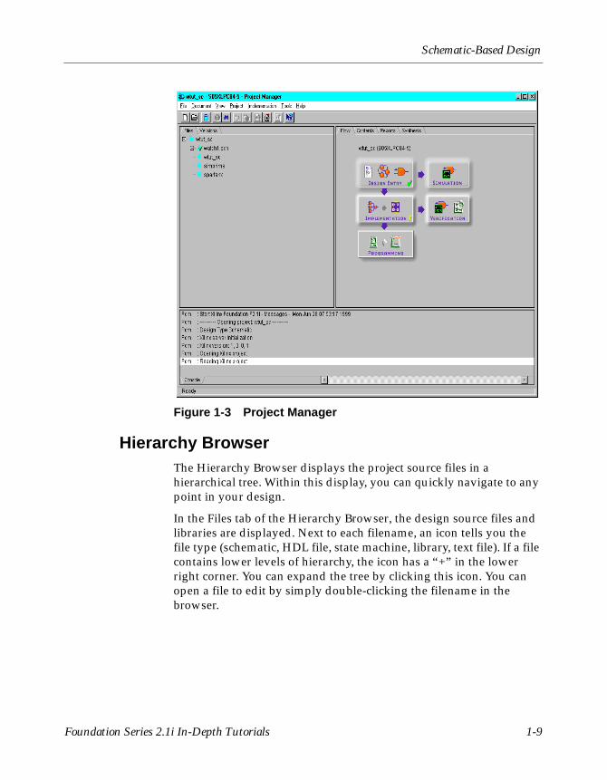
The Project ManagerThe Project Manager controls all aspects of the design flow.You can access all of the various design entry and design implementation tools as well as the files and documents associated with your project. The Project Manager also maintains revision control over multiple design iterations.
The Project Manager is divided into three main subwindows. To the left is the Design Hierarchy Browser which displays the project elements. To the right is a set of tabs, each one opens a separate functional window. The third window at the bottom of the Project Manager is the Message Console and shows status messages, errors, and warnings, and is updated during all project actions. These windows are discussed in more detail in the following sections.
1-8 Xilinx Development System
Schematic-Based Design
Figure 1-3 Project Manager
Hierarchy BrowserThe Hierarchy Browser displays the project source files in a hierarchical tree. Within this display, you can quickly navigate to any point in your design.
In the Files tab of the Hierarchy Browser, the design source files and libraries are displayed. Next to each filename, an icon tells you the file type (schematic, HDL file, state machine, library, text file). If a file contains lower levels of hierarchy, the icon has a “+” in the lower right corner. You can expand the tree by clicking this icon. You can open a file to edit by simply double-clicking the filename in the browser.
Foundation Series 2.1i In-Depth Tutorials 1-9

Foundation Series 2.1i In-Depth Tutorials
A Versions tab is also available behind the Files tab. This tab displays a design’s implementation revisions. Because this is a new design which has not yet been implemented, the Versions tab does not yet contain any revision information. Versions are discussed in more detail later in the tutorial during design implementation.
Project Manager Functional TabsAs mentioned previously, the right-hand side of the Project Manager contains a series of functional tabs. Briefly, the functions of these tabs follow.
• Flow—Provides access to tools you use to complete your entire design, arranged in a flow-chart style to guide you through the design flow. Status indicators in the lower right corner of each phase button indicate whether the step has been completed successfully.
• Contents—Lists contents and date the file selected in the Hierarchy Browser was last modified.
• Reports—Displays design flow reports.
• Synthesis—Displays all of the HDL macros contained in the project, and, from this tab, you can update these macros.
You have the option to browse through these tabs to see how the tabs are updated during the design flow process.
Message Console WindowErrors, warnings, and informational messages are displayed in the Message Window. Errors are displayed in red, warnings in blue, and informational messages in black.
Design EntryIn this hierarchical design, you will create various types of macros, including schematic-based macros, HDL-based macros, state machine macros, and LogiBLOX macros. You will learn the process for creating each of these types of macros, and then you will connect them all together to create the completed Watch design. This tutorial gives you experience with creating and using each type of design macro so that you can apply this knowledge to your own design.
1-10 Xilinx Development System

Schematic-Based Design
Starting the Schematic EditorThere are two different ways to open the Schematic Capture tool.
• From the Flow tab, click the Schematic Capture icon in the Design Entry phase button. This instructs the Schematic Editor to open the project’s top level schematic sheet.
• Double click the file name WATCH.SCH in the Files tab.
The Schematic Editor opens with the Watch schematic sheet loaded. The Watch schematic is incomplete at this point. Throughout the tutorial, you create the components to complete the design. The unfinished design is shown in the figure below.
Foundation Series 2.1i In-Depth Tutorials 1-11

Foundation Series 2.1i In-Depth Tutorials
Figure 1-4 Incomplete Watch Schematic
If you need to stop the tutorial at any time, save your work by selecting File → Save from the pulldown menus.
Executing CommandsThere are three ways to execute commands within the Foundation tools: pulldown menus, hotkeys, and toolbar buttons. In most cases, this tutorial instructs you to use the pulldown menus.
Hotkeys
You can use the keyboard to execute various commands. These “hotkeys” are listed next to the commands within the pulldown menus. Some of the hotkeys are the function keys, some are single letters, and some require the Ctrl or Alt keys. You cannot customize them.
Toolbar Buttons
There are also toolbars that are located beneath the pulldown menus and to the left of the main Schematic Editor window. Hold your mouse over the buttons to see their function.
1-12 Xilinx Development System

Schematic-Based Design
Figure 1-5 Schematic Editor
Manipulating the ScreenUnder the Display pulldown menu is a series of commands that modify the viewing area of the Schematic Editor window. Zoom in the schematic to comfortably view it.
Foundation Series 2.1i In-Depth Tutorials 1-13
Foundation Series 2.1i In-Depth Tutorials
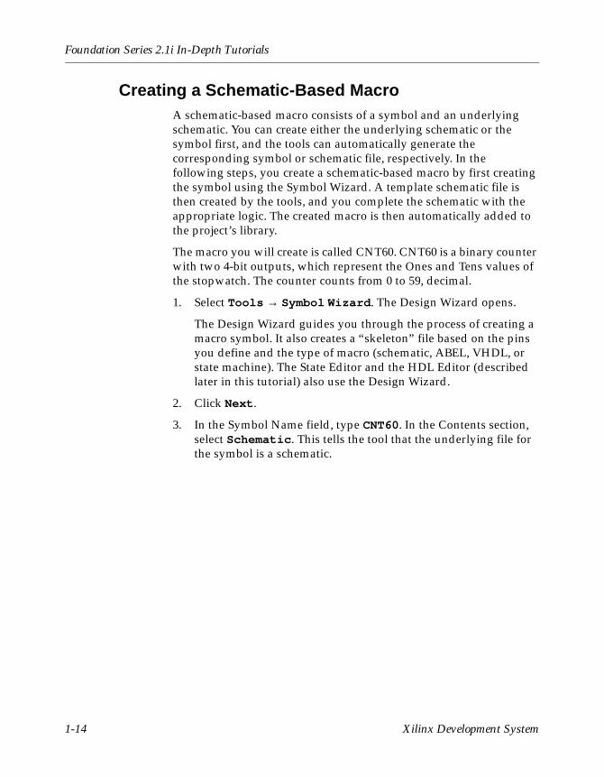
Creating a Schematic-Based MacroA schematic-based macro consists of a symbol and an underlying schematic. You can create either the underlying schematic or the symbol first, and the tools can automatically generate the corresponding symbol or schematic file, respectively. In the following steps, you create a schematic-based macro by first creating the symbol using the Symbol Wizard. A template schematic file is then created by the tools, and you complete the schematic with the appropriate logic. The created macro is then automatically added to the project’s library.
The macro you will create is called CNT60. CNT60 is a binary counter with two 4-bit outputs, which represent the Ones and Tens values of the stopwatch. The counter counts from 0 to 59, decimal.
1. Select Tools → Symbol Wizard. The Design Wizard opens.
The Design Wizard guides you through the process of creating a macro symbol. It also creates a “skeleton” file based on the pins you define and the type of macro (schematic, ABEL, VHDL, or state machine). The State Editor and the HDL Editor (described later in this tutorial) also use the Design Wizard.
2. Click Next.
3. In the Symbol Name field, type CNT60. In the Contents section, select Schematic. This tells the tool that the underlying file for the symbol is a schematic.
1-14 Xilinx Development System
Schematic-Based Design
Figure 1-6 Symbol Wizard - Contents Page
4. Click Next.
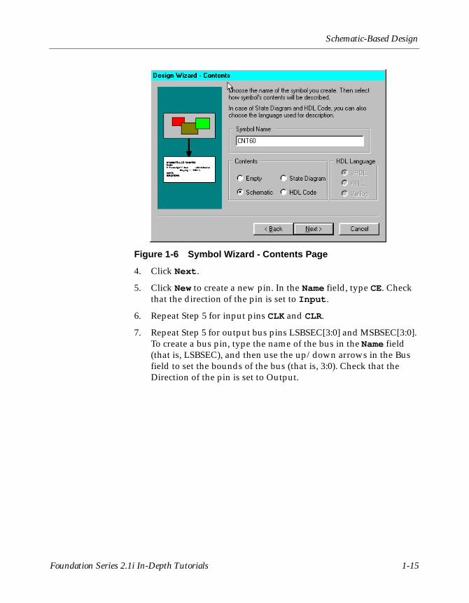
5. Click New to create a new pin. In the Name field, type CE. Check that the direction of the pin is set to Input.
6. Repeat Step 5 for input pins CLK and CLR.
7. Repeat Step 5 for output bus pins LSBSEC[3:0] and MSBSEC[3:0]. To create a bus pin, type the name of the bus in the Name field (that is, LSBSEC), and then use the up/down arrows in the Bus field to set the bounds of the bus (that is, 3:0). Check that the Direction of the pin is set to Output.
Foundation Series 2.1i In-Depth Tutorials 1-15
Foundation Series 2.1i In-Depth Tutorials
Figure 1-7 Symbol Wizard - Ports Page
8. Click Next.
Note: In the Comments section, you can type text that appears on the symbol when it is placed. You can also define a longer comment that only appears in the SC Symbols window when you place components.
9. Click Next and then click Finish.
The symbol is created and placed in the project library and can be accessed from the SC Symbols toolbox. The Symbol Wizard automatically creates and opens a schematic sheet with I/O terminals corresponding to the defined symbol pins.
Note: If the schematic is not automatically created, the most likely cause is that Empty was selected in step 4. Repeat steps 1-9, and click Yes or OK when prompted to overwrite the existing symbol.
1-16 Xilinx Development System
Schematic-Based Design
Creating the CNT60 SchematicYou have now created the symbol for CNT60 with the help of the Symbol Wizard. The next step is to create the underlying corresponding schematic for this macro. You can then reference this macro symbol by placing it on a schematic sheet.
Opening the Schematic
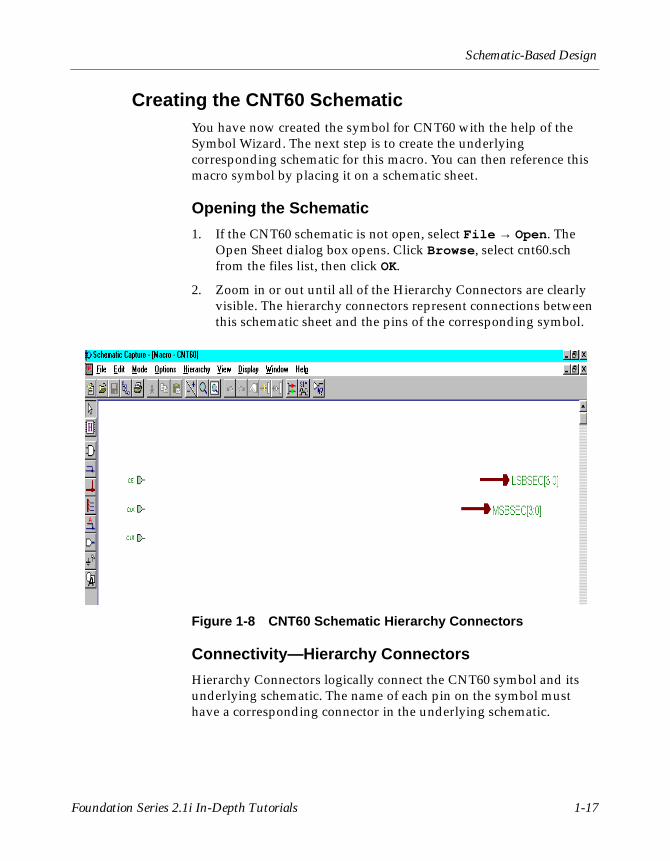
1. If the CNT60 schematic is not open, select File → Open. The Open Sheet dialog box opens. Click Browse, select cnt60.sch from the files list, then click OK.
2. Zoom in or out until all of the Hierarchy Connectors are clearly visible. The hierarchy connectors represent connections between this schematic sheet and the pins of the corresponding symbol.
Figure 1-8 CNT60 Schematic Hierarchy Connectors
Connectivity—Hierarchy Connectors
Hierarchy Connectors logically connect the CNT60 symbol and its underlying schematic. The name of each pin on the symbol must have a corresponding connector in the underlying schematic.
Foundation Series 2.1i In-Depth Tutorials 1-17
Foundation Series 2.1i In-Depth Tutorials
The Symbol Wizard automatically places hierarchy connectors on the schematic. If you need to add hierarchy connectors manually, you can use the Hierarchy Connector icon in the vertical toolbar.
When you save a macro, the Schematic Editor checks the hierarchy connectors against the corresponding symbol. If there is a discrepancy, you can let the software update the symbol automatically, or you can modify the symbol manually. Hierarchy connectors should only be used to connect signals between levels of hierarchy. Never use hierarchy connectors on top-level schematic sheets.
Project Libraries
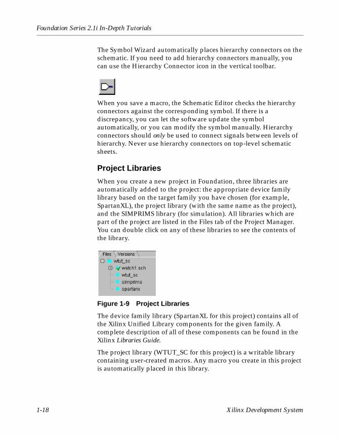
When you create a new project in Foundation, three libraries are automatically added to the project: the appropriate device family library based on the target family you have chosen (for example, SpartanXL), the project library (with the same name as the project), and the SIMPRIMS library (for simulation). All libraries which are part of the project are listed in the Files tab of the Project Manager. You can double click on any of these libraries to see the contents of the library.
Figure 1-9 Project Libraries
The device family library (SpartanXL for this project) contains all of the Xilinx Unified Library components for the given family. A complete description of all of these components can be found in the Xilinx Libraries Guide.
The project library (WTUT_SC for this project) is a writable library containing user-created macros. Any macro you create in this project is automatically placed in this library.
1-18 Xilinx Development System
Schematic-Based Design
Additionally, you can copy macros from other libraries into this project library and vice versa using the Schematic Symbols Library Manager which you can open with the Tools → Utilities menu in the Project Manager.
To facilitate simulation with the Foundation Logic Simulator, the SIMPRIMS is added to the project. This library contains the simulation models for the Xilinx devices.
You can add more libraries to the project by choosing File → Project Libraries from the Project Manager. After you add a library to the project, you can use any component from that library in the current project.
Adding Components to CNT60
Components from all of the libraries (except SIMPRIMS) for the given project are available from the SC Symbols toolbox to place on the schematic. The available components listed in this toolbox are arranged alphabetically within each library.
1. From the menu bar, select Mode → Symbols or click the Symbols Toolbox button in the vertical toolbar on the left side of the Schematic Editor.
This opens the SC Symbols window and displays the libraries and their corresponding components.
Foundation Series 2.1i In-Depth Tutorials 1-19

Foundation Series 2.1i In-Depth Tutorials
Figure 1-10 SC Symbols Toolbox
2. The first component you will place is an AND2, a 2-input AND gate. You can select this component by either scrolling down the list and selecting it or by typing AND2 in the bottom of the SC Symbols Window. Then move the mouse back into the schematic window.
In the SC Symbols window, when the AND2 component is selected, a description of the component appears in the bottom of the window.
3. Move the symbol outline to the location shown in the following figure and click the left mouse button to place the object.
1-20 Xilinx Development System
Schematic-Based Design
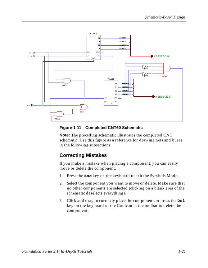
Figure 1-11 Completed CNT60 Schematic
Note: The preceding schematic illustrates the completed CNT schematic. Use this figure as a reference for drawing nets and buses in the following subsections.
Correcting Mistakes
If you make a mistake when placing a component, you can easily move or delete the component.
1. Press the Esc key on the keyboard to exit the Symbols Mode.
2. Select the component you want to move or delete. Make sure that no other components are selected (clicking on a blank area of the schematic deselects everything).
3. Click and drag to correctly place the component, or press the Del key on the keyboard or the Cut icon in the toolbar to delete the component.
Foundation Series 2.1i In-Depth Tutorials 1-21
Foundation Series 2.1i In-Depth Tutorials
Placing the Remaining Components
Follow the steps listed previously in the “Adding Components to CNT60” section to place the CD4CE, OR2, CB4RE, INV, and AND4 components on the schematic sheet as shown in the “Completed CNT60 Schematic” figure. For a detailed description of the functionality of each of these components, refer to the Xilinx Libraries Guide.
Moving Hierarchy Terminals
To make the schematic easier to draw and clearer to read, move some of the hierarchy connectors which were automatically created by the Symbol Wizard. Follow these steps to relocate the hierarchy connectors as shown in the “Completed CNT60 Schematic” figure.
1. With the mouse cursor in point/select mode, select the CLR hierarchy connector, and drag it to the lower left area of the schematic sheet. If the mouse cursor is not in point/select mode, Press the Esc key on the keyboard to get into this mode.
2. To move the bus hierarchy terminal MSBSEC[3:0], select and drag an area surrounding the entire bus hierarchy terminal and label it, so that both the bus and the label are highlighted in red. With the bus and label highlighted, click on the terminal again, and drag the entire unit down to the lower right area of the sche-matic sheet. Release the mouse to place the terminal, and then click anywhere else on the schematic sheet to deselect the bus and label.
Drawing Nets
You use the Draw Wires icon in the vertical toolbar to draw wires (also called nets) between the various components on the schematic. Use Nets to physically connect single bits together.
Signals can also logically be connected by naming multiple segments identically. In this case, the nets do not need to be physically connected on the schematic to make the logical connection. In the CNT60 schematic, you will draw nets to connect the components together. Do not yet worry about drawing the nets for the LSBSEC and MSBSEC buses. These nets will be drawn in the next section.
Follow these steps to draw a net between the AND2 and the CB4RE components on the CNT60 schematic.
1-22 Xilinx Development System
Schematic-Based Design
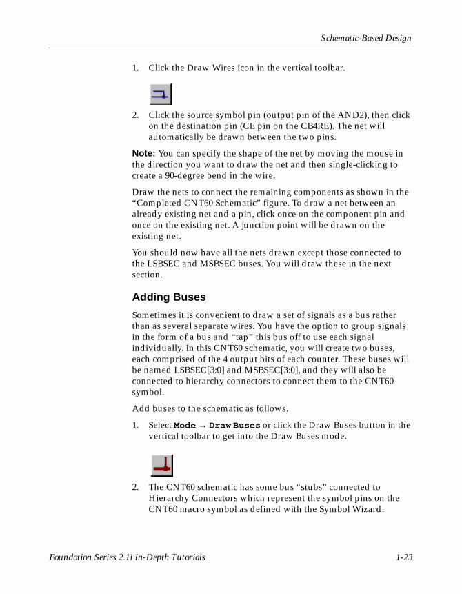
1. Click the Draw Wires icon in the vertical toolbar.
2. Click the source symbol pin (output pin of the AND2), then click on the destination pin (CE pin on the CB4RE). The net will automatically be drawn between the two pins.
Note: You can specify the shape of the net by moving the mouse in the direction you want to draw the net and then single-clicking to create a 90-degree bend in the wire.
Draw the nets to connect the remaining components as shown in the “Completed CNT60 Schematic” figure. To draw a net between an already existing net and a pin, click once on the component pin and once on the existing net. A junction point will be drawn on the existing net.
You should now have all the nets drawn except those connected to the LSBSEC and MSBSEC buses. You will draw these in the next section.
Adding Buses
Sometimes it is convenient to draw a set of signals as a bus rather than as several separate wires. You have the option to group signals in the form of a bus and “tap” this bus off to use each signal individually. In this CNT60 schematic, you will create two buses, each comprised of the 4 output bits of each counter. These buses will be named LSBSEC[3:0] and MSBSEC[3:0], and they will also be connected to hierarchy connectors to connect them to the CNT60 symbol.
Add buses to the schematic as follows.
1. Select Mode → Draw Buses or click the Draw Buses button in the vertical toolbar to get into the Draw Buses mode.
2. The CNT60 schematic has some bus “stubs” connected to Hierarchy Connectors which represent the symbol pins on the CNT60 macro symbol as defined with the Symbol Wizard.
Foundation Series 2.1i In-Depth Tutorials 1-23
Foundation Series 2.1i In-Depth Tutorials
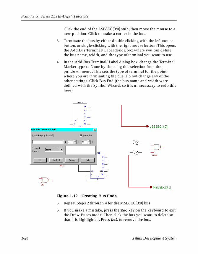
Click the end of the LSBSEC[3:0] stub, then move the mouse to a new position. Click to make a corner in the bus.
3. Terminate the bus by either double clicking with the left mouse button, or single-clicking with the right mouse button. This opens the Add Bus Terminal/Label dialog box where you can define the bus name, width, and the type of terminal you want to use.
4. In the Add Bus Terminal/Label dialog box, change the Terminal Marker type to None by choosing this selection from the pulldown menu. This sets the type of terminal for the point where you are terminating the bus. Do not change any of the other settings. Click Bus End (the bus name and width were defined with the Symbol Wizard, so it is unnecessary to redo this here).
Figure 1-12 Creating Bus Ends
5. Repeat Steps 2 through 4 for the MSBSEC[3:0] bus.
6. If you make a mistake, press the Esc key on the keyboard to exit the Draw Buses mode. Then click the bus you want to delete so that it is highlighted. Press Del to remove the bus.
1-24 Xilinx Development System
Schematic-Based Design
7. After adding the two buses, press Esc or right-click to exit the Draw Buses mode.
Adding Bus Taps
Next, you add nets to attach the appropriate pins from the CB4RE and CD4CE counters to the buses. Use Bus Taps to tap off a single bit of a bus and connect it to another component. The Schematic Capture tool can automatically name the bus taps incrementally as they are drawn.
You have the option to enlarge the view of the schematic to make it easier to draw the nets.
1. Select Mode → Draw Bus Taps or click the Draw Bus Taps button in the vertical toolbar. The cursor changes, indicating that you are now in Draw Bus Taps mode.
2. Click the LSBSEC[3:0] bus label.
The status bar at the bottom of the window displays the message Expand Bus Tap: LSBSEC3. This tells you that the next bus tap drawn will be labeled LSBSEC3.
Note: The default is to start at 3 and decrement as bus taps are drawn. You can use the up and down arrow keys to change which bus bit will be tapped first.
3. Click the Q3 output pin of the CD4CE component to draw the bus tap. The net is automatically drawn and labeled. The status bar now reads Expand Bus Tap: LSBSEC2.
4. Click next on each of the other output pins of the CD4CE component. The bus taps will be drawn and labeled incrementally.
Note: If the bits are not automatically being labeled incrementally, check that you clicked the bus name (label) before clicking the counter output pins.
Note: If the nets appear disconnected, try selecting Display → Redraw to refresh the screen.
Foundation Series 2.1i In-Depth Tutorials 1-25
Foundation Series 2.1i In-Depth Tutorials
If there is an error with the labeling of the bus taps, double click the bus tap net to edit the label.
5. Repeat Steps 1 through 4 for the MSBSEC[3:0] bus.
6. Press Esc twice or right-click to exit the Draw Bus Taps mode.
7. Complete the schematic by drawing the nets to connect the MSBSEC bus taps to the INV and AND4 components. If necessary, refer to the “Drawing Nets” section for guidance.
8. Compare your CNT60 schematic again with the “Completed CNT60 Schematic” figure to ensure that all connections are properly made.
Saving the Schematic
The CNT60 schematic is now complete.
Save the schematic by selecting File → Save or clicking the Save icon in the horizontal toolbar.
All errors, warnings, and informational messages are displayed in the Message Window in the Project Manager. If any errors are issued, resolve them and save the schematic again.
Placing the CNT60 Macro
So far, you have created the CNT60 macro. The next step is to place this macro on the top-level Watch schematic sheet, where it may then be connected to other components in the design.
1. Open the Watch schematic sheet. If the Watch schematic is already open, you will see a tab at the bottom of the Schematic Capture tool where you can select that sheet.
2. If the Watch schematic is not open, select File → Open, select the Watch sheet, and click OK.
3. Open the SC Symbols Toolbox to display a list of all the available design components. As mentioned before, you can select the Symbols Toolbox icon to open the SC Symbols Toolbox.
1-26 Xilinx Development System
Schematic-Based Design
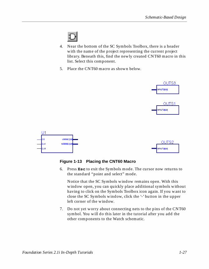
4. Near the bottom of the SC Symbols Toolbox, there is a header with the name of the project representing the current project library. Beneath this, find the newly created CNT60 macro in this list. Select this component.
5. Place the CNT60 macro as shown below.
Figure 1-13 Placing the CNT60 Macro
6. Press Esc to exit the Symbols mode. The cursor now returns to the standard “point and select” mode.
Notice that the SC Symbols window remains open. With this window open, you can quickly place additional symbols without having to click on the Symbols Toolbox icon again. If you want to close the SC Symbols window, click the ‘-’ button in the upper left corner of the window.
7. Do not yet worry about connecting nets to the pins of the CNT60 symbol. You will do this later in the tutorial after you add the other components to the Watch schematic.
Foundation Series 2.1i In-Depth Tutorials 1-27
Foundation Series 2.1i In-Depth Tutorials
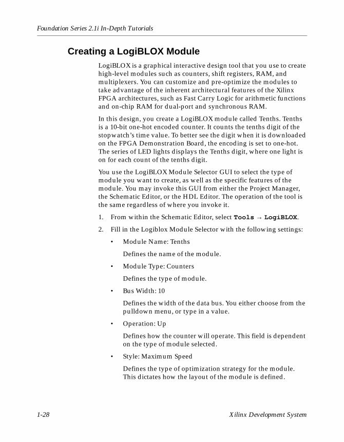
Creating a LogiBLOX ModuleLogiBLOX is a graphical interactive design tool that you use to create high-level modules such as counters, shift registers, RAM, and multiplexers. You can customize and pre-optimize the modules to take advantage of the inherent architectural features of the Xilinx FPGA architectures, such as Fast Carry Logic for arithmetic functions and on-chip RAM for dual-port and synchronous RAM.
In this design, you create a LogiBLOX module called Tenths. Tenths is a 10-bit one-hot encoded counter. It counts the tenths digit of the stopwatch’s time value. To better see the digit when it is downloaded on the FPGA Demonstration Board, the encoding is set to one-hot. The series of LED lights displays the Tenths digit, where one light is on for each count of the tenths digit.
You use the LogiBLOX Module Selector GUI to select the type of module you want to create, as well as the specific features of the module. You may invoke this GUI from either the Project Manager, the Schematic Editor, or the HDL Editor. The operation of the tool is the same regardless of where you invoke it.
1. From within the Schematic Editor, select Tools → LogiBLOX.
2. Fill in the Logiblox Module Selector with the following settings:
• Module Name: Tenths
Defines the name of the module.
• Module Type: Counters
Defines the type of module.
• Bus Width: 10
Defines the width of the data bus. You either choose from the pulldown menu, or type in a value.
• Operation: Up
Defines how the counter will operate. This field is dependent on the type of module selected.
• Style: Maximum Speed
Defines the type of optimization strategy for the module. This dictates how the layout of the module is defined.
1-28 Xilinx Development System
Schematic-Based Design
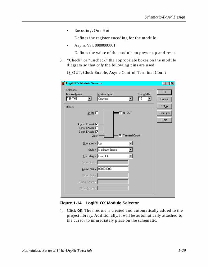
• Encoding: One Hot
Defines the register encoding for the module.
• Async Val: 0000000001
Defines the value of the module on power-up and reset.
3. “Check” or “uncheck” the appropriate boxes on the module diagram so that only the following pins are used.
Q_OUT, Clock Enable, Async Control, Terminal Count
Figure 1-14 LogiBLOX Module Selector
4. Click OK. The module is created and automatically added to the project library. Additionally, it will be automatically attached to the cursor to immediately place on the schematic.
Foundation Series 2.1i In-Depth Tutorials 1-29

Foundation Series 2.1i In-Depth Tutorials
Note: If you do not want to place the symbol at this time, you can press the Esc key on the keyboard to get out of the Place Symbol mode. You can then select it at any time from the SC Symbols Toolbox to place on the schematic.
5. Place the newly created Tenths component on the Watch schematic sheet, as shown below. You will connect this symbol to the rest of the schematic later in the tutorial. The symbol is labeled “L1” on the schematic sheet.
Figure 1-15 Placing the Logiblox TENTHS component
6. Save the schematic by selecting File → Save. Close the Sche-matic Editor.
Creating a State Machine ModuleWith the Foundation State Editor, you graphically create finite state machines. You draw states, inputs/outputs, and state transition conditions on the diagram using a simple windows GUI. Transition conditions and state actions are typed into the diagram in appropriate VHDL, Verilog, or ABEL syntax. The State Editor then synthesizes the diagram into either VHDL, Verilog or ABEL code. The resulting HDL file is finally synthesized to create a netlist and/or macro for you to place on a schematic sheet.
1-30 Xilinx Development System
Schematic-Based Design
For this tutorial, a partially complete state machine diagram is provided. In the next section, you complete the diagram and synthesize the module into a macro to place on the Watch schematic. Both a VHDL and an ABEL version of the State Machine diagram have been provided for you.
If you have a Foundation Express package, you can use either the VHDL or ABEL version. If you have a Foundation Standard or a Foundation Base package, then you must use the ABEL version of the diagram.
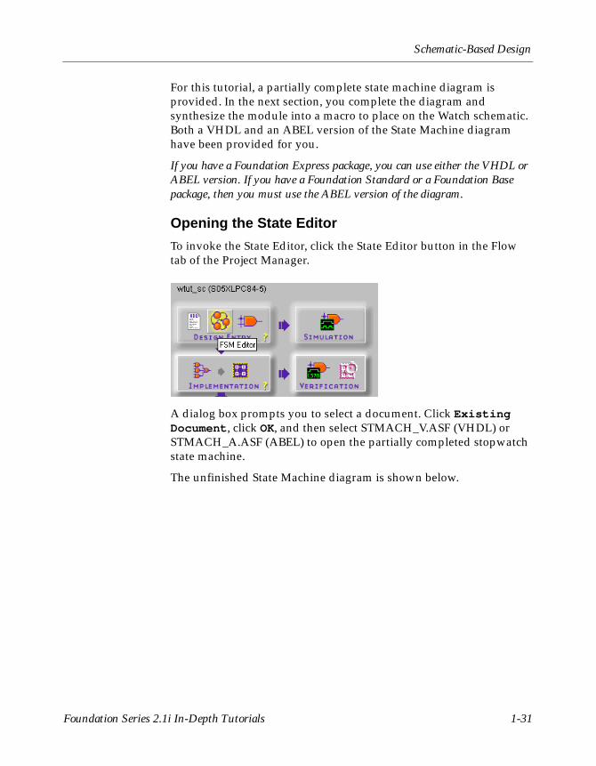
Opening the State Editor
To invoke the State Editor, click the State Editor button in the Flow tab of the Project Manager.
A dialog box prompts you to select a document. Click Existing Document, click OK, and then select STMACH_V.ASF (VHDL) or STMACH_A.ASF (ABEL) to open the partially completed stopwatch state machine.
The unfinished State Machine diagram is shown below.
Foundation Series 2.1i In-Depth Tutorials 1-31
Foundation Series 2.1i In-Depth Tutorials
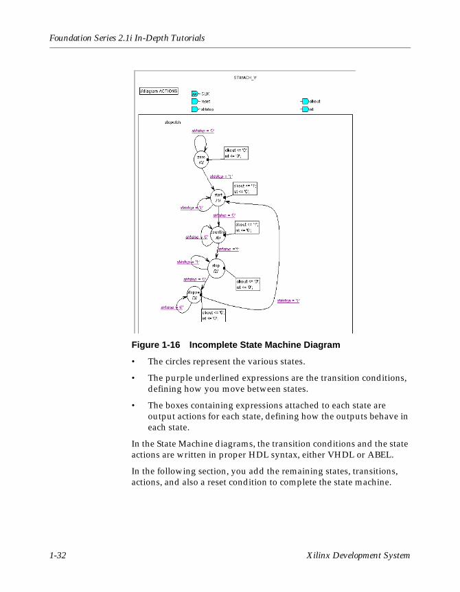
Figure 1-16 Incomplete State Machine Diagram
• The circles represent the various states.
• The purple underlined expressions are the transition conditions, defining how you move between states.
• The boxes containing expressions attached to each state are output actions for each state, defining how the outputs behave in each state.
In the State Machine diagrams, the transition conditions and the state actions are written in proper HDL syntax, either VHDL or ABEL.
In the following section, you add the remaining states, transitions, actions, and also a reset condition to complete the state machine.
1-32 Xilinx Development System
Schematic-Based Design
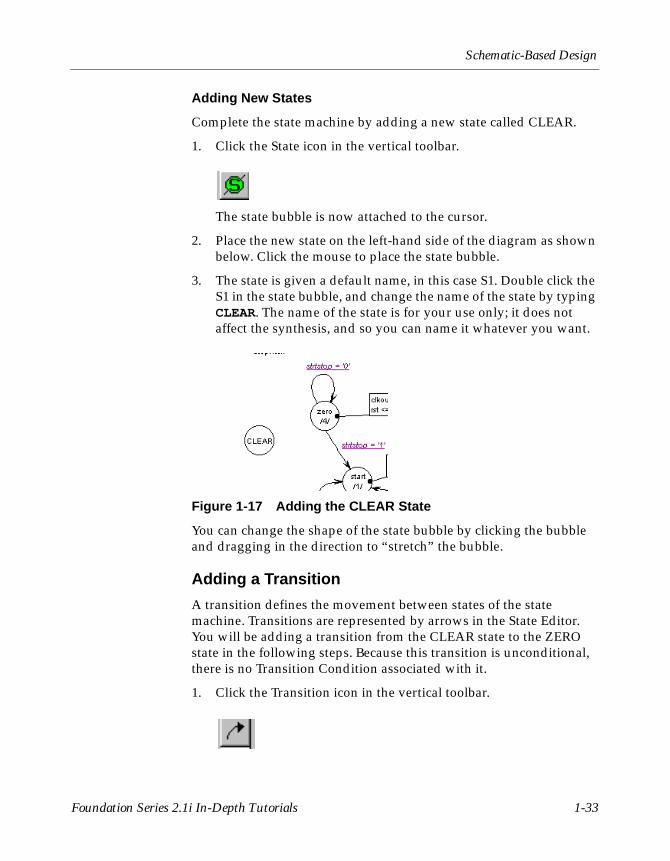
Adding New States
Complete the state machine by adding a new state called CLEAR.
1. Click the State icon in the vertical toolbar.
The state bubble is now attached to the cursor.
2. Place the new state on the left-hand side of the diagram as shown below. Click the mouse to place the state bubble.
3. The state is given a default name, in this case S1. Double click the S1 in the state bubble, and change the name of the state by typing CLEAR. The name of the state is for your use only; it does not affect the synthesis, and so you can name it whatever you want.
Figure 1-17 Adding the CLEAR State
You can change the shape of the state bubble by clicking the bubble and dragging in the direction to “stretch” the bubble.
Adding a Transition
A transition defines the movement between states of the state machine. Transitions are represented by arrows in the State Editor. You will be adding a transition from the CLEAR state to the ZERO state in the following steps. Because this transition is unconditional, there is no Transition Condition associated with it.
1. Click the Transition icon in the vertical toolbar.
Foundation Series 2.1i In-Depth Tutorials 1-33

Foundation Series 2.1i In-Depth Tutorials
2. Click first on the CLEAR state, then on the ZERO state to draw the transition arrow. The arrow’s shape can be manipulated by clicking it and then dragging the mouse.
Figure 1-18 Adding State Transition
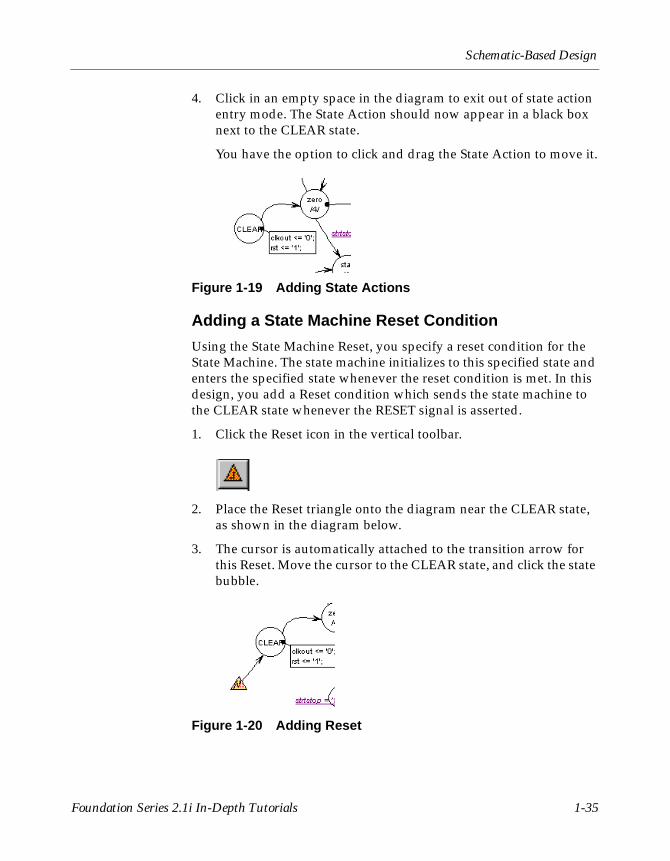
Adding a State Action
A State Action dictates how the outputs should behave in a given state. There are three types of state actions: Entry Action, State Action, and Exit Action. These determine if the outputs should act upon entry to, existence in, or exit from a given state, respectively.
You will add two state actions to the CLEAR state, one to drive the CLKOUT output to 0, and one to drive the RST output to 1.
1. Click the State Action icon in the vertical toolbar.
2. Move the mouse over the diagram so that the small round ball at the end of the pointer is over the CLEAR state. After you are in this position, click the mouse to place the State Action box.
3. When a cursor appears, type the following state action:
• For ABEL:
clkout = 0;
rst = 1;
• For VHDL:
clkout <= ‘0’;
rst <= ‘1’;
1-34 Xilinx Development System
Schematic-Based Design
4. Click in an empty space in the diagram to exit out of state action entry mode. The State Action should now appear in a black box next to the CLEAR state.
You have the option to click and drag the State Action to move it.
Figure 1-19 Adding State Actions
Adding a State Machine Reset Condition
Using the State Machine Reset, you specify a reset condition for the State Machine. The state machine initializes to this specified state and enters the specified state whenever the reset condition is met. In this design, you add a Reset condition which sends the state machine to the CLEAR state whenever the RESET signal is asserted.
1. Click the Reset icon in the vertical toolbar.
2. Place the Reset triangle onto the diagram near the CLEAR state, as shown in the diagram below.
3. The cursor is automatically attached to the transition arrow for this Reset. Move the cursor to the CLEAR state, and click the state bubble.
Figure 1-20 Adding Reset
Foundation Series 2.1i In-Depth Tutorials 1-35

Foundation Series 2.1i In-Depth Tutorials
Adding a Transition Condition
Add the Transition Condition to the Reset. Transition Conditions are applied to all transitions, not only Reset transitions, in the same way. Transition Conditions are attached to the transition arrows, and describe the required condition for the movement between states.
Add a transition condition which tells the state machine to reset to the CLEAR state whenever the signal RESET is high.
1. Click the Condition icon in the vertical toolbar.
2. Click the transition arrow which was drawn between the Reset triangle and the CLEAR state.
3. When the cursor appears, type in the following condition:
• For ABEL:
reset
• For VHDL:
reset = ‘1’
4. Click in an empty space in the diagram to exit the Draw Condition mode. The condition should now appear underlined and in purple text.
Figure 1-21 Adding Reset Transition Condition
5. Save your changes by selecting File → Save .
1-36 Xilinx Development System
Schematic-Based Design
Creating the State Machine Macro
You will now synthesize the state machine and a macro will be created that you can place on the Watch schematic. The macro symbol will automatically be added to the project library. The synthesis process encompasses the creation of the HDL code from the state machine diagram and the synthesis of the HDL code by either the Foundation Express (VHDL) or XABEL (ABEL) compiler. Additionally, you have the option to use the State Editor to create a symbol for the state machine which you can place on the schematic.
1. Select Project → Create Macro. This synthesizes the design as well as creates the macro symbol and adds the symbol to the SC Symbols toolbox.
2. To view the HDL code which the State Editor produced, select Tools → HDL Editor.
3. Close the State Editor by clicking the X in the upper right corner of the window.
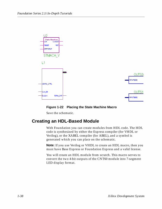
Placing the STMACH symbol
You can now place the STMACH state machine macro on the Watch schematic. If it is not already opened, open the Schematic Editor. Open the SC Symbols Toolbox to view the list of available library components. You should now be able to locate the STMACH_A or STMACH_V macro in this list. (If the SC Symbols Toolbox was already open, and you do not see the STMACH macro, select File → Update Libraries.) Select the appropriate symbol, and add it to the Watch schematic as shown below. Do not worry about drawing the wires to connect this symbol. You will connect the entire schematic later in the tutorial.
Foundation Series 2.1i In-Depth Tutorials 1-37
Foundation Series 2.1i In-Depth Tutorials
Figure 1-22 Placing the State Machine Macro
Save the schematic.
Creating an HDL-Based ModuleWith Foundation you can create modules from HDL code. The HDL code is synthesized by either the Express compiler (for VHDL or Verilog), or the XABEL compiler (for ABEL), and a symbol is generated which you can place on the schematic.
Note: If you use Verilog or VHDL to create an HDL macro, then you must have Base Express or Foundation Express and a valid license.
You will create an HDL module from scratch. This macro serves to convert the two 4-bit outputs of the CNT60 module into 7-segment LED display format.
1-38 Xilinx Development System
Schematic-Based Design
Using the HDL Design Wizard and HDL Editor
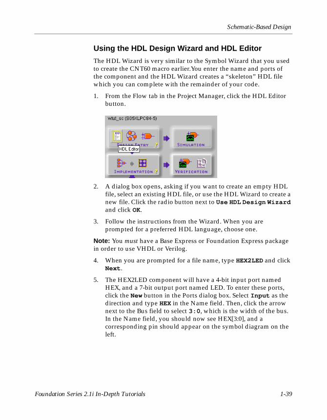
The HDL Wizard is very similar to the Symbol Wizard that you used to create the CNT60 macro earlier.You enter the name and ports of the component and the HDL Wizard creates a “skeleton” HDL file which you can complete with the remainder of your code.
1. From the Flow tab in the Project Manager, click the HDL Editor button.
2. A dialog box opens, asking if you want to create an empty HDL file, select an existing HDL file, or use the HDL Wizard to create a new file. Click the radio button next to Use HDL Design Wizard and click OK.
3. Follow the instructions from the Wizard. When you are prompted for a preferred HDL language, choose one.
Note: You must have a Base Express or Foundation Express package in order to use VHDL or Verilog.
4. When you are prompted for a file name, type HEX2LED and click Next.
5. The HEX2LED component will have a 4-bit input port named HEX, and a 7-bit output port named LED. To enter these ports, click the New button in the Ports dialog box. Select Input as the direction and type HEX in the Name field. Then, click the arrow next to the Bus field to select 3:0, which is the width of the bus. In the Name field, you should now see HEX[3:0], and a corresponding pin should appear on the symbol diagram on the left.
Foundation Series 2.1i In-Depth Tutorials 1-39
Foundation Series 2.1i In-Depth Tutorials
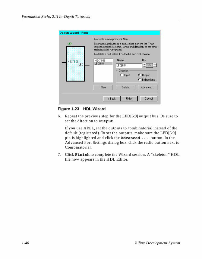
Figure 1-23 HDL Wizard
6. Repeat the previous step for the LED[6:0] output bus. Be sure to set the direction to Output.
If you use ABEL, set the outputs to combinatorial instead of the default (registered). To set the outputs, make sure the LED[6:0] pin is highlighted and click the Advanced ... button. In the Advanced Port Settings dialog box, click the radio button next to Combinatorial.
7. Click Finish to complete the Wizard session. A “skeleton” HDL file now appears in the HDL Editor.
1-40 Xilinx Development System
Schematic-Based Design
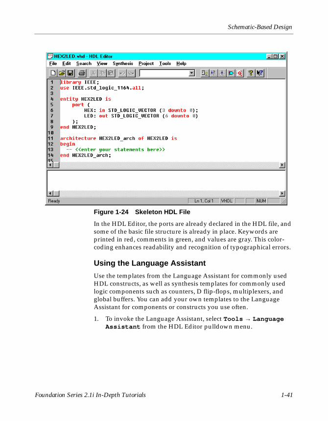
Figure 1-24 Skeleton HDL File
In the HDL Editor, the ports are already declared in the HDL file, and some of the basic file structure is already in place. Keywords are printed in red, comments in green, and values are gray. This color-coding enhances readability and recognition of typographical errors.
Using the Language Assistant
Use the templates from the Language Assistant for commonly used HDL constructs, as well as synthesis templates for commonly used logic components such as counters, D flip-flops, multiplexers, and global buffers. You can add your own templates to the Language Assistant for components or constructs you use often.
1. To invoke the Language Assistant, select Tools → Language Assistant from the HDL Editor pulldown menu.
Foundation Series 2.1i In-Depth Tutorials 1-41

Foundation Series 2.1i In-Depth Tutorials
2. The Language Assistant is divided into three sections: Language Templates, Synthesis Templates and User Templates. To expand the view of any of these sections, click the ‘+’ next to the topic. Click any of the listed templates to view the template in the right hand pane.
3. Use the template called HEX2LED Converter located under the Synthesis Templates heading. Locate this template, preview it in the right hand pane by clicking the template. This template provides source code to convert a 4-bit value to 7-segment LED display format.
Figure 1-25 HDL Language Assistant
4. Before adding this template to your HDL file, be sure that the cursor in the HDL Editor is positioned below the line with the comments “<<enter your statements here>>” for VHDL. For Verilog, enter code after the “// Add your code here” line. For ABEL, add the template below the line “<<add your equations here>>”. When you use the template, the code is placed wherever the cursor is currently positioned in the HDL Editor.
5. To add the HEX2LED Converter template code, click the Use button in the Language Assistant while the HEX2LED Converter template is selected. The code is automatically placed in the HDL file.
6. Close the Language Assistant by clicking the X in the upper right corner of the window.
1-42 Xilinx Development System

Schematic-Based Design
7. (Verilog only) After the “//add your declarations here” statement and before the HEX2LED converter that you just added, add the following line of code to the HDL file to allow an assignment.
reg LED;
8. You now have complete and functional HDL code and can check the syntax using Synthesis → Check Syntax.
9. After you successfully complete the syntax check, save the file by selecting File → Save from the HDL Editor.
Synthesizing the HDL Code and Creating a Macro
Synthesize the code and create a macro symbol which may be placed on the schematic.
1. From within the HDL Editor, select Project → Create Macro.
The code is synthesized, and a symbol is created and placed in the project library.
2. Close the HDL Editor by clicking the X in the upper right corner of the window.
Adding the HEX2LED Component to the Schematic
You are now ready to place the HEX2LED macro on the Watch schematic. Open the Schematic Editor if it is not already open. Open the SC Symbols Toolbox (refer to the “Adding Components to CNT60” section) to view the list of available library components. You should now be able to locate the HEX2LED macro in this list. Select it, and add it to the Watch schematic as shown in the next figure.
This component will be placed on the Watch schematic sheet in two separate instances. To duplicate the component in the schematic, click the left mouse button while the pointer is on the placed symbol, and then click again to place the duplicate symbol.
Note: The Symbols Toolbox icon must still be depressed on the vertical toolbar to enable this feature to automatically duplicate a symbol.
Again, do not worry about drawing the wires and buses to connect this macro. You will connect the entire schematic later in the tutorial.
Foundation Series 2.1i In-Depth Tutorials 1-43
Foundation Series 2.1i In-Depth Tutorials
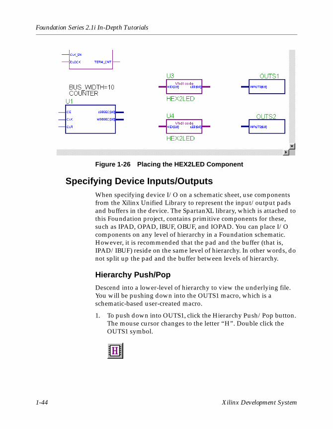
Figure 1-26 Placing the HEX2LED Component
Specifying Device Inputs/OutputsWhen specifying device I/O on a schematic sheet, use components from the Xilinx Unified Library to represent the input/output pads and buffers in the device. The SpartanXL library, which is attached to this Foundation project, contains primitive components for these, such as IPAD, OPAD, IBUF, OBUF, and IOPAD. You can place I/O components on any level of hierarchy in a Foundation schematic. However, it is recommended that the pad and the buffer (that is, IPAD/IBUF) reside on the same level of hierarchy. In other words, do not split up the pad and the buffer between levels of hierarchy.
Hierarchy Push/Pop
Descend into a lower-level of hierarchy to view the underlying file. You will be pushing down into the OUTS1 macro, which is a schematic-based user-created macro.
1. To push down into OUTS1, click the Hierarchy Push/Pop button. The mouse cursor changes to the letter “H”. Double click the OUTS1 symbol.
1-44 Xilinx Development System

Schematic-Based Design
In the OUTS1 schematic, you see a series of output buffers (OBUF) and output pads (OPAD). These represent output pins on the SpartanXL device. Each of these pads has a LOC=P__ attribute attached to them. This attribute assigns each of the pins to a particular pin on the target device. You will add more pins with LOC attributes in the next section.
Figure 1-27 OUTS1 Schematic Macro
The OUTS2 and OUTS3 macros are similar to OUTS1, except that the pins have been locked to different device I/O.
2. “Pop” back out of the OUTS1 component. You can do this in one of two ways. Either click the Hierarchy Push/Pop icon, then double click in an empty space in the OUTS1 schematic, or click the Watch tab at the bottom of the Schematic Capture tool to return to the top-level Watch schematic sheet.
Foundation Series 2.1i In-Depth Tutorials 1-45

Foundation Series 2.1i In-Depth Tutorials
Adding Input Pins
Add three more input pins to the Watch schematic, called CLK, RESET and STRTSTOP.
1. Add an IPAD and an IBUF for each of the two input pins, RESET and STRTSTOP. Add an IPAD and a BUFG for the input clock signal, CLK. To add these components, click the SC Symbols icon in the vertical toolbar to open the SC Symbols Toolbox. Browse to locate the IPAD, IBUF, and BUFG components in the SpartanXL library. Drop these on the schematic as shown below.
2. Draw a net between each IPAD/IBUF pair and the IPAD/BUFG input. If necessary, refer to the section on drawing nets (see the “Drawing Nets” section) for instruction.
Figure 1-28 Placing CLK, RESET and STRTSTOP I/O Components
1-46 Xilinx Development System

Schematic-Based Design
Labeling NetsIt is important to label nets and buses for several reasons. It aids in debugging and simulation, as you will more easily trace nets back to your original design. Any nets which remain unnamed in the design will be given machine-generated names which will mean nothing to you later in the implementation process. Naming nets also enhances readability and aids in documenting your design.
Label the three input nets you just drew. When naming input and output pins, it is advisable to label the net between the pad and the buffer. This name is carried through the entire design flow including place and route. If you label only the output of the buffer (in the case of an input pin) or input of the buffer (in the case of an output pin), you will not be able to easily trace your I/O pins in implementation tools and reports.
1. Double click the RESET net.
2. In the Net Name field, type RESET as shown below.
Figure 1-29 Labeling Nets
3. Click OK.
4. Repeat Steps 1 through 3 for the STRTSTOP and CLK pins. You have the option to click and drag the new attributes to better place them on the schematic.
Foundation Series 2.1i In-Depth Tutorials 1-47
Foundation Series 2.1i In-Depth Tutorials
Figure 1-30 Labeled Nets
Assigning Pin LocationsXilinx recommends that you let the automatic placement and routing program, PAR, define the pinout of your design. Pre-assigning locations to the pins can sometimes degrade the performance of the place and route tools. However, it is usually necessary, at some point, to lock the pinout of a design so that it can be integrated into a PCB (Printed Circuit Board).
Define the initial pinout by running the place-and-route tools without pin assignments, then locking down the pin placement so that it reflects the locations chosen by the tools. In this design, you assign locations to the pins in the Watch design so that the design can function in a Xilinx demonstration board. Because the design is simple and timing is not critical, these pin assignments will not adversely affect the ability of PAR to place and route the design.
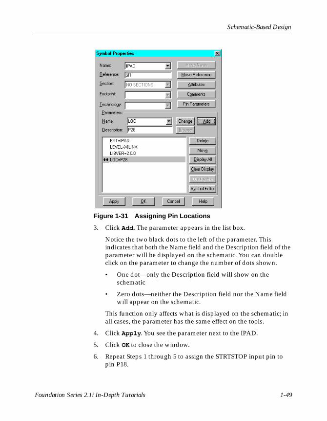
Specify pin locations by attaching a LOC parameter to a pad component. Assign a LOC parameter to the pad associated with the RESET signal on the Watch schematic as follows.
1. Double click the IPAD connected to the net labeled RESET. The Symbol Properties dialog box opens.
2. In the Parameters section, add a new parameter with these values:
Name: LOC
Description: P28
This step assigns the RESET signal to pin P28 of the target device.
1-48 Xilinx Development System
Schematic-Based Design
Figure 1-31 Assigning Pin Locations
3. Click Add. The parameter appears in the list box.
Notice the two black dots to the left of the parameter. This indicates that both the Name field and the Description field of the parameter will be displayed on the schematic. You can double click on the parameter to change the number of dots shown.
• One dot—only the Description field will show on the schematic
• Zero dots—neither the Description field nor the Name field will appear on the schematic.
This function only affects what is displayed on the schematic; in all cases, the parameter has the same effect on the tools.
4. Click Apply. You see the parameter next to the IPAD.
5. Click OK to close the window.
6. Repeat Steps 1 through 5 to assign the STRTSTOP input pin to pin P18.
Foundation Series 2.1i In-Depth Tutorials 1-49
Foundation Series 2.1i In-Depth Tutorials
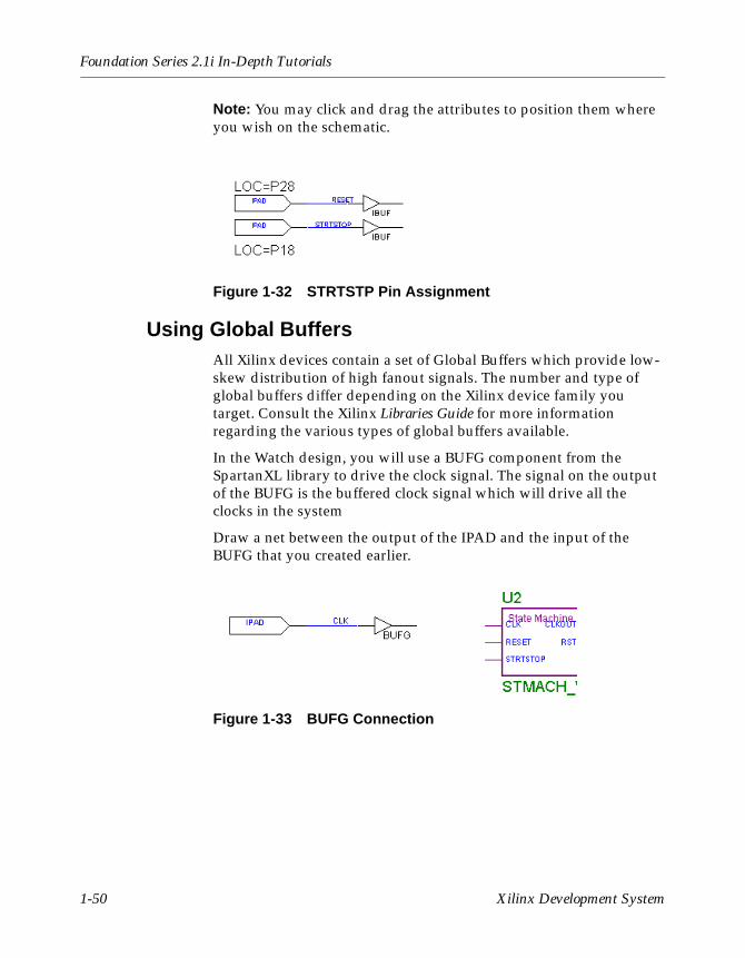
Note: You may click and drag the attributes to position them where you wish on the schematic.
Figure 1-32 STRTSTP Pin Assignment
Using Global BuffersAll Xilinx devices contain a set of Global Buffers which provide low-skew distribution of high fanout signals. The number and type of global buffers differ depending on the Xilinx device family you target. Consult the Xilinx Libraries Guide for more information regarding the various types of global buffers available.
In the Watch design, you will use a BUFG component from the SpartanXL library to drive the clock signal. The signal on the output of the BUFG is the buffered clock signal which will drive all the clocks in the system
Draw a net between the output of the IPAD and the input of the BUFG that you created earlier.
Figure 1-33 BUFG Connection
1-50 Xilinx Development System
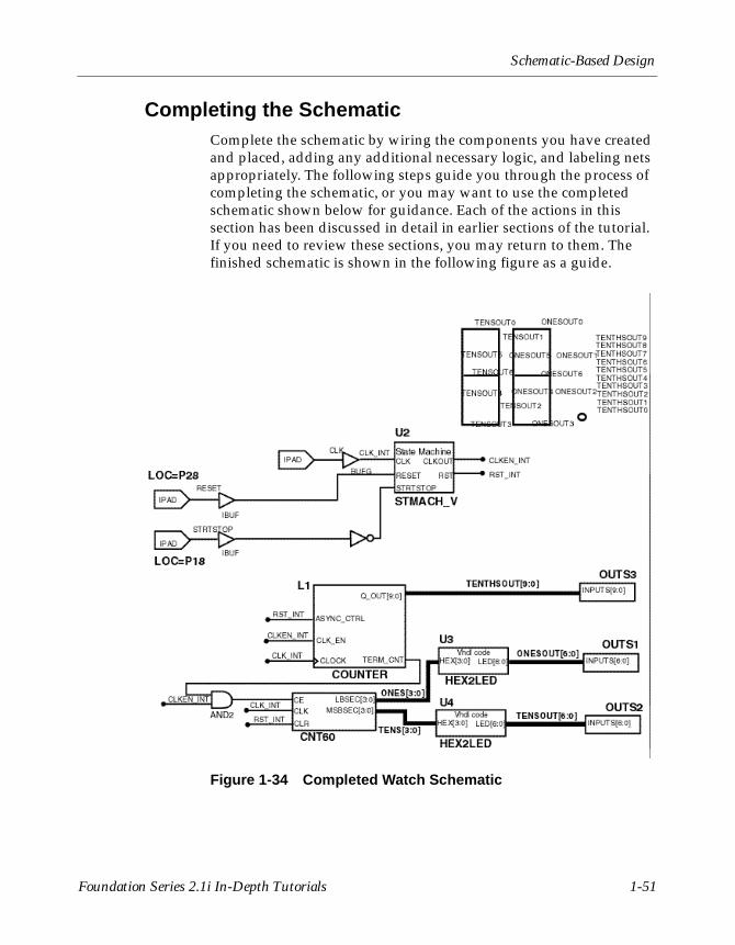
Schematic-Based Design
Completing the SchematicComplete the schematic by wiring the components you have created and placed, adding any additional necessary logic, and labeling nets appropriately. The following steps guide you through the process of completing the schematic, or you may want to use the completed schematic shown below for guidance. Each of the actions in this section has been discussed in detail in earlier sections of the tutorial. If you need to review these sections, you may return to them. The finished schematic is shown in the following figure as a guide.
Figure 1-34 Completed Watch Schematic
Foundation Series 2.1i In-Depth Tutorials 1-51

Foundation Series 2.1i In-Depth Tutorials
1. Draw a net (see the “Drawing Nets” section) between the BUFG and the CLK pin of the STMACH state machine macro. Label this net CLK_INT.
2. Draw a net (see the “Drawing Nets” section) between the IBUF of the RESET input and the RESET pin of the STMACH state machine macro.
3. Place an INV (inverter) component (see the “Adding Components to CNT60” section) from the SpartanXL library between the IBUF of the STRTSTOP input and the STRTSTOP pin of the STMACH state machine macro. Draw nets (see the “Drawing Nets” section) to connect the INV to the both the IBUF and the STMACH state machine macro.
4. Place an AND2 component (see the “Adding Components to CNT60” section) to the left of the CNT60 macro.
5. Draw a net (see the “Drawing Nets” section) to connect the output of the AND2 with the CE pin of the CNT60 macro.
6. Draw a net (see the “Drawing Nets” section) to connect the TERM_CNT pin of the TENTHS macro to one of the inputs to the AND2.
7. Draw a hanging net (see the “Drawing Nets” section) from the CLKOUT pin of the STMACH macro. To terminate a hanging wire, double click.
8. Press Esc to get back into point/select mode and then label the net you drew in Step 7 CLKEN_INT.
9. Draw a hanging net at the CLK_EN input pin of the TENTHS macro. Label this net CLKEN_INT (see the “Labeling Nets” section).
10. Draw a hanging net (see the “Drawing Nets” section) at the other input of the AND2 component. Label this net CLKEN_INT again (see the “Labeling Nets” section).
11. Draw a hanging net (see the “Drawing Nets” section) from the RST output pin of the STMACH macro. Label this net RST_INT.
12. Draw two more hanging nets (see the “Drawing Nets” section), also named RST_INT, from the ASYNC_CTRL pin of the TENTHS macro and from the CLR pin of the CNT60 macro.
1-52 Xilinx Development System

Schematic-Based Design
13. Draw two hanging nets (see the “Drawing Nets” section), each named CLK_INT, from the CLOCK pin of the TENTHS macro and from the CLK pin of the CNT60 macro.
Note: Remember that nets are logically connected if their names are the same, even if the net is not physically drawn as a connection in the schematic. This method is used to make the logical connection of the RST_INT, CLKEN_INT and CLK_INT signals.
14. Draw buses (see the “Adding Buses” section) to complete the schematic. Label them as shown on the preceding schematic diagram.
The schematic is now complete!
15. Save the design by selecting File → Save.
Foundation Series 2.1i In-Depth Tutorials 1-53

Foundation Series 2.1i In-Depth Tutorials
1-54 Xilinx Development System
Chapter 2
HDL-Based Design
This chapter guides you through a typical HDL-based design procedure using a design of a runner’s stopwatch called Watch. The design example used in this tutorial demonstrates many device features, software features and design flow practices which you can apply to your own design. This design targets an SpartanXL device; however, all of the principles and flows taught are applicable to any Xilinx device family, unless otherwise noted.
For an example of how to design with CPLDs, see the online help by selecting Help → Foundation Help Contents from the Project Manager. Under Tutorials, select CPLD Design Flows.
In the first part of the tutorial, you use the Foundation design entry tools to complete the design. The design is composed of HDL elements and a LogiBLOX macro; you will synthesize the design using the Express tools.
Then, you will functionally simulate the design using the Foundation Logic Simulator. In the third part, you will implement the design using the Xilinx Implementation Tools. The simulation, implementation, and bitstream generation are described in subsequent chapters.
This chapter includes the following sections.
• “Getting Started”
• “Design Description”
• “The Project Manager”
• “Design Entry”
• “Synthesizing the Design”
• “The Express Constraints Editor (Foundation Express Only)”
Foundation Series 2.1i In-Depth Tutorials 2-1
Foundation Series 2.1i In-Depth Tutorials
• “Using the Express Constraints Editor (Foundation Express Only)”
• “Viewing Synthesis Results (Foundation Express Only)”
Getting StartedThe following subsections describe the basic requirements for running the tutorial.
NomenclatureIn this tutorial, the following terms are used:
• “Spartan family” includes the Spartan and SpartanXL devices only.
• “Right-click” means click the right mouse button. Unless specified, all other mouse operations are performed with the left mouse button.
Throughout this tutorial, file names, project names, and directory names (paths) are specified in lower case, and the design is referred to as Watch.
Required SoftwareThe Xilinx Foundation Series package, Version 2.1i, is required to perform this tutorial. The design requires that you have installed the SpartanXL libraries and device files and are licensed for Foundation Express or Base Express. You must also have the Watch projects which are installed with the Sample Designs or which may be downloaded from http://support.xilinx.com.
Note: A Foundation Express license is required to access the Express Constraints GUI.
Installing the TutorialThis tutorial assumes that the software is installed in the default location c:\fndtn. If you have installed the software in a different location, substitute your installation path for c:\fndtn.
The tutorial projects are optionally installed (as sample projects) in the c:\fndtn\active\projects directory when you install the
2-2 Xilinx Development System

HDL-Based Design
Foundation Series software. If you have installed the software, but are not sure whether the tutorial projects were installed, check for directories named c:\fndtn\active\projects\wtut*. These directories contain the various tutorial files.
Note: For detailed instructions, refer to the Foundation Series 2.1i Install and Release Document.
Tutorial Project Directories and FilesDuring the software installation, the WTUT_VHD and WTUT_VER directories are created within c:\fndtn\active\projects, and the tutorial files are copied into these directories. These directories contain complete and incomplete versions of the design, done in VHDL and Verilog, respectively. You will complete the design in the tutorial. However, solutions projects with all completed input and output files are also provided. The following table lists the associated project.
The WATCHVHD and WATCHVER solution projects contain the design files for the completed tutorials, including HDL files and the bitstream file.To conserve disk space, some intermediate files are not provided. Do not overwrite any files in the solutions directories.
The WTUT_VHD and WTUT_VER projects contain incomplete copies of the tutorial design. You will create the remaining files when you perform the tutorial. As described in a later step, you have the option to copy the Watch project to another area and perform the tutorial in this new area if desired.
VHDL or Verilog?This tutorial has been prepared for both VHDL and Verilog designs. This document applies to both designs simultaneously, noting differences where applicable. You will need to decide which HDL
Table 2-1 Tutorial Project Directories
Directory Description
WTUT_VHD Incomplete Watch Tutorial - VHDL
WTUT_VER Incomplete Watch Tutorial - Verilog
WATCHVHD Solution for Watch - VHDL
WATCHVER Solution for Watch - Verilog
Foundation Series 2.1i In-Depth Tutorials 2-3
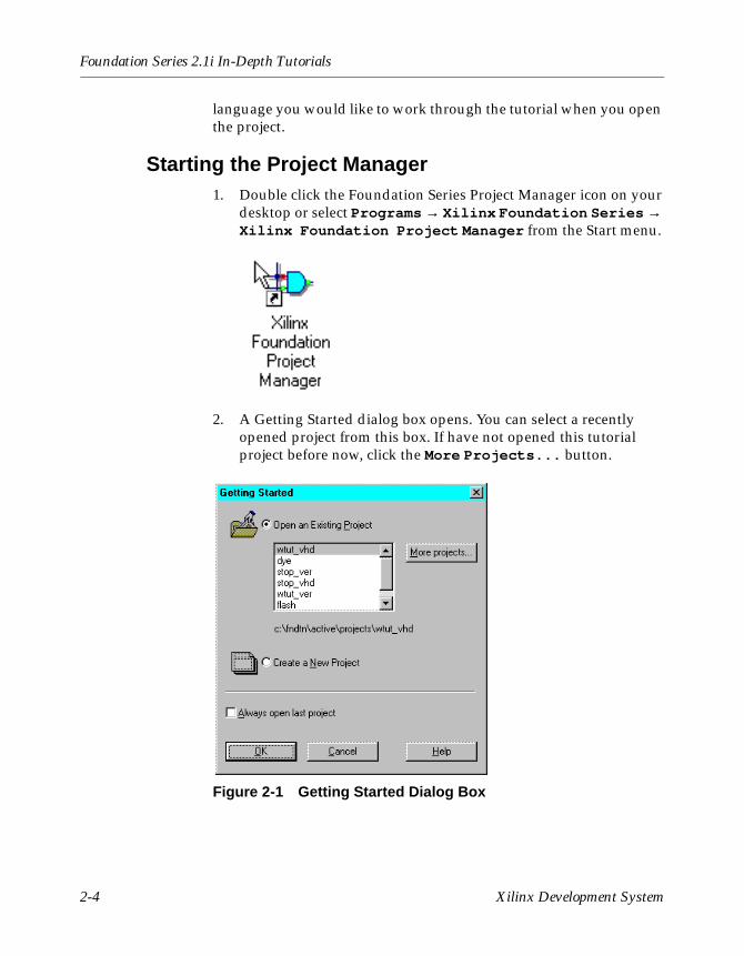
Foundation Series 2.1i In-Depth Tutorials
language you would like to work through the tutorial when you open the project.
Starting the Project Manager1. Double click the Foundation Series Project Manager icon on your
desktop or select Programs → Xilinx Foundation Series → Xilinx Foundation Project Manager from the Start menu.
2. A Getting Started dialog box opens. You can select a recently opened project from this box. If have not opened this tutorial project before now, click the More Projects... button.
Figure 2-1 Getting Started Dialog Box
2-4 Xilinx Development System
HDL-Based Design
3. In the Directories list, browse to c:\fndtn\active\projects. In the Projects list, open WTUT_VHD or WTUT_VER by double clicking.
Copying the Tutorial Files (Optional)You can either work within the project directory as it has been installed from the CD, or you can make a copy to work on. To make a working copy of the tutorial files, begin with an opened project and perform the following steps.
Note: Whenever copying projects in Foundation, it is important to use the “Copy Project” feature in the Project Manager to ensure that the project’s directory structure is kept intact.
1. Select File → Copy Project.
2. Under the Destination section, type “wtch_hdl” in the Name field.
3. Click OK.
4. Select File → Open Project.
5. Scroll down in the project list and select the wtch_hdl project name. Click Open.
6. The wtch_hdl project will contain two UCF files. If this is the case, select wtut_vhd.ucf or wtut_ver.ucf. Select Document → Remove or press Del to remove the file (wtut_ver.ucf or wtut_vhd.ucf). Click Yes to confirm the removal of the file.
This does not delete the file from the disk. It merely removes it from the project so that it is not used during compilation. The file still exists in the project directory on the disk. If you mistakenly remove a file from a project, select Document → Add to add it back.
Design DescriptionThe design used in this tutorial is a hierarchical, HDL-based design, meaning that the top-level design file is an HDL file that references several other lower-level macros. The lower-level macros are either HDL modules or LogiBLOX modules.
Foundation Series 2.1i In-Depth Tutorials 2-5

Foundation Series 2.1i In-Depth Tutorials
The design begins as an unfinished design. Throughout the tutorial, you complete the design by generating some of the modules from scratch and by completing some others from existing files. When the design is complete, you simulate it to verify the design’s functionality.
Watch is a simple runner’s stopwatch. There are three external inputs, and three external output buses in the completed design. The system clock is an externally generated signal. The following list summarizes the input lines and output buses.
Inputs:
• STRTSTOP —Starts and stops the stopwatch. This is an active low signal which acts like the start/stop button on a runner’s stopwatch.
• RESET—Resets the stopwatch to 00.0 after it has been stopped.
• CLK—Externally generated system clock
Outputs:
• TENSOUT[6:0]—7-bit bus which represents the Ten’s digit of the stopwatch value. This bus is in 7-segment display format viewable on the 7-segment LED display on the Xilinx demonstration board.
• ONESOUT[6:0]—Similar to TENSOUT bus above, but represents the One’s digit of the stopwatch value.
• TENTHSOUT[9:0]—10-bit bus which represents the Tenths’ digit of the stopwatch value. This bus is one-hot encoded.
The completed design consists of the following functional blocks.
• STATMACH
State Machine module.
• CNT60
HDL-based module which counts from 0 to 59, decimal. This macro has 2 4-bit outputs, which represent the ones and tens digits of the decimal values, respectively.
• TENTHS
Logiblox 10-bit, one-hot encoded counter. This macro outputs the tenths digit of the watch value as a 10-bit one-hot encoded value.
2-6 Xilinx Development System

HDL-Based Design
• HEX2LED
HDL-based macro. This macro decodes the ones and tens digit values from hexadecimal to 7-segment display format for viewing on the FPGA Demonstration Board.
• SMALLCNTR
A simple Counter.
Foundation Series 2.1i In-Depth Tutorials 2-7
Foundation Series 2.1i In-Depth Tutorials
The Project ManagerThe Project Manager controls all aspects of the design flow. Through the Project Manager, you can access all of the various design entry and design implementation tools. You can also access the files and documents associated with your project. The Project Manager maintains revision control over multiple design iterations.
The Project Manager is divided into three main subwindows. To the left is the Design Hierarchy Browser which displays the elements included in the project. To the right is a set of tabs, each one brings up a separate functional window. The third window at the bottom of the Project Manager is the Message Console and shows status messages, errors, and warnings and is updated during all project actions. These windows are discussed in more detail in the following sections.
Figure 2-2 Project Manager
2-8 Xilinx Development System

HDL-Based Design
Hierarchy BrowserIn the Files tab of the Hierarchy Browser, design source files and libraries are displayed. Next to each filename is an icon which tells you the file type (HDL file, state machine, schematic, library, text file, for example). If a file contains lower levels of hierarchy, the icon has a + to the left of the name. HDL files have this + to show the entities (VHDL) or modules (Verilog) within the file. You can expand the tree by clicking this icon. You can open a file to edit by double clicking the filename in the browser.
A Versions tab is also available behind the Files tab. Since this is a new design which has not yet been implemented, the Versions tab is empty. This tab is discussed in more detail later in the tutorial during design implementation.
Project Manager Functional TabsAs mentioned previously, the right-hand side of the Project Manager contains a series of functional tabs. The functions of these tabs follows:
• Flow—Provides access to tools you use to complete your entire design, arranged in a flow-chart style to guide you through the design flow. Status indicators in the upper right corner of each phase box indicate whether the step has been completed successfully.
• Contents—Lists the contents and date of the last modification of the file selected in the Hierarchy Browser.
• Reports—Accesses design flow reports.
You have the option to browse through these tabs at this time, and at any time during the tutorial to see how the tabs are updated during the design flow process.
Foundation Series 2.1i In-Depth Tutorials 2-9
Foundation Series 2.1i In-Depth Tutorials
Message Console WindowErrors, warnings, and informational messages are displayed in the Message Window. Errors are displayed in red, warnings in blue, and informational messages in black.
Information about synthesis results are displayed under the HDL Errors, HDL Warnings, and HDL Messages tabs. Because the HDL messages, errors and warnings are associated with a specific file or version, you must select a synthesis version (functional structure or optimized structure) or a specific file in the Files or Version tab to see messages.
Design EntryIn this hierarchical design, you will examine HDL files, correct syntax errors, create an HDL macro, and add a LogiBLOX module. This tutorial gives you experience with creating and using each type of design macro so that you can apply these procedures to your own design.
Adding Source FilesYou must add HDL files to the project before they can be synthesized. Four HDL files have already been added to this project, but have not yet been analyzed. Use Synthesis → Analyze All Source Files to update these files.
Now add the remaining HDL file to the project. Select Synthesis → Add Source Files and select SMALLCNTR.VHD or SMALLCNTR.V from the project directory.
This file will be analyzed when it is added to the project. HDL files that have been added to the project always have one of four status indicators associated with the file. These indicators are:
• A red question mark means the file has been modified and needs to be re-analyzed. Right-click the file and select Analyze.
• A red X means errors have been found. Select this file and examine the errors under the HDL Errors tab. Errors are also given in the HDL Editor.
2-10 Xilinx Development System
HDL-Based Design
• A red exclamation point means warnings have been issued. Select the file and examine the warnings under the HDL Warnings tab. Many warnings can be safely ignored.
• A green check means that the file is up-to-date with no errors or warnings.
Correcting HDL errorsThe SMALLCNTR design contains a syntax error that must be corrected. The red “x” next to the filename indicates an error was found during analysis. The Project Manager reports errors in red and warnings in blue in the console.
Note: To open help on Express errors or warnings, select the error or message in the HDL Error or Warning tab, then press the F1 key.
1. Open SMALLCNTR.VHD or SMALLCNTR.V in the HDL Editor by double clicking the file name in the Files tab of the Hierarchy Browser.
2. Correct any errors in the HDL source file. The comments next to the error explain this simple fix.
3. Select File → Save to save the file.
4. Re-analyze the file by selecting Synthesis → Check Syntax, in the HDL Editor or by right-clicking the HDL file in the Project Manager and selecting Analyze.
Foundation Series 2.1i In-Depth Tutorials 2-11

Foundation Series 2.1i In-Depth Tutorials
Starting the HDL EditorThere are three different ways to open the HDL Editor tool.
• From the Flow tab, click the HDL icon within the Design Entry phase button.
• Double click an HDL file in the Files tab.
• Right-click an HDL file in the Files tab and select Edit.
If you need to stop the tutorial at any time, save your work by selecting File → Save from the menus.
Creating an HDL-Based ModuleWith Foundation, you can easily create modules from HDL code. The HDL code is connected to your top-level HDL design through instantiation and compiled with the rest of the design.
You will create a new HDL module. This macro serves to convert the two 4-bit outputs of the CNT60 module into a 7-segment LED display format.
Using the HDL Design Wizard and HDL Editor
You enter the name and ports of the component in the HDL Wizard and the Wizard creates a “skeleton” HDL file which you can complete with the remainder of your code.
2-12 Xilinx Development System
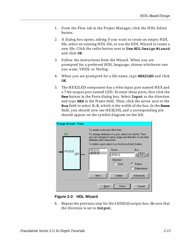
HDL-Based Design
1. From the Flow tab in the Project Manager, click the HDL Editor button.
2. A dialog box opens, asking if you want to create an empty HDL file, select an existing HDL file, or use the HDL Wizard to create a new file. Click the radio button next to Use HDL Design Wizard and click OK.
3. Follow the instructions from the Wizard. When you are prompted for a preferred HDL language, choose whichever one you want, VHDL or Verilog.
4. When you are prompted for a file name, type HEX2LED and click OK.
5. The HEX2LED component has a 4-bit input port named HEX and a 7-bit output port named LED. To enter these ports, first click the New button in the Ports dialog box. Select Input as the direction and type HEX in the Name field. Then, click the arrow next to the Bus field to select 3:0, which is the width of the bus. In the Name field, you should now see HEX[3:0], and a corresponding pin should appear on the symbol diagram on the left.
Figure 2-3 HDL Wizard
6. Repeat the previous step for the LED[6:0] output bus. Be sure that the direction is set to Output.
Foundation Series 2.1i In-Depth Tutorials 2-13

Foundation Series 2.1i In-Depth Tutorials
7. Click Finish to complete the Wizard session. A “skeleton” HDL file now displays in the HDL Editor.
Figure 2-4 Skeleton VHDL File
2-14 Xilinx Development System
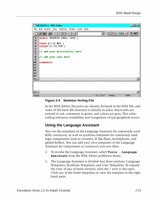
HDL-Based Design
Figure 2-5 Skeleton Verilog File
In the HDL Editor, the ports are already declared in the HDL file, and some of the basic file structure is already in place. Keywords are printed in red, comments in green, and values are gray. This color-coding enhances readability and recognition of typographical errors.
Using the Language Assistant
You use the templates in the Language Assistant for commonly used HDL constructs, as well as synthesis templates for commonly used logic components such as counters, D flip-flops, multiplexers, and global buffers. You can add your own templates to the Language Assistant for components or constructs you use often.
1. To invoke the Language Assistant, select Tools → Language Assistant from the HDL Editor pulldown menu.
2. The Language Assistant is divided into three sections: Language Templates, Synthesis Templates, and User Templates. To expand the view of any of these sections, click the + next to the topic. Click any of the listed templates to view the template in the right hand pane.
Foundation Series 2.1i In-Depth Tutorials 2-15
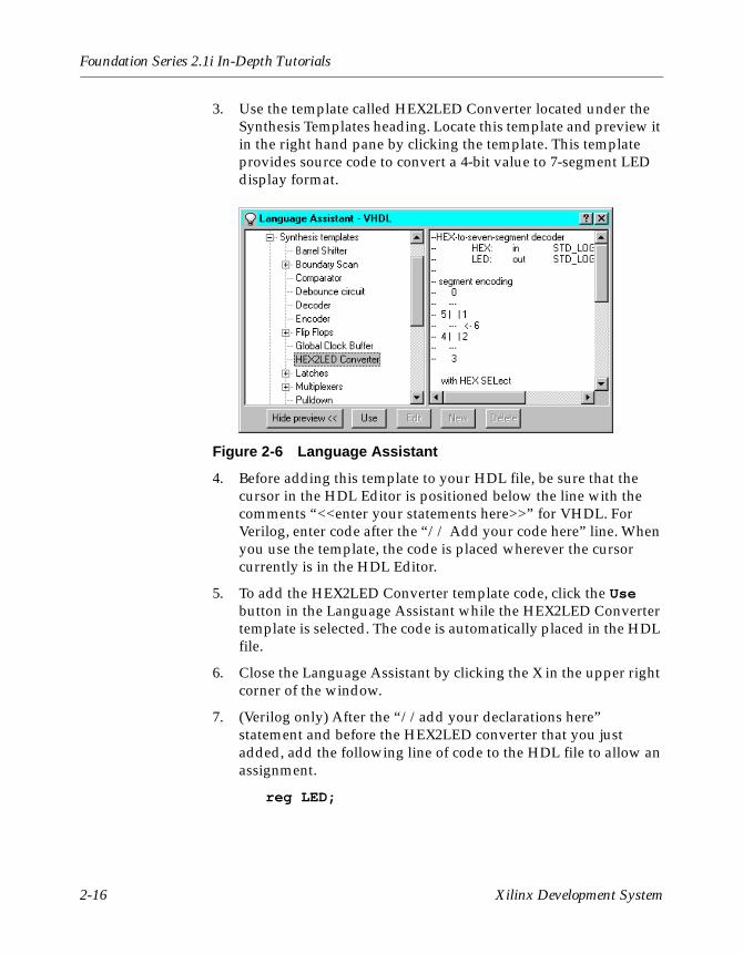
Foundation Series 2.1i In-Depth Tutorials
3. Use the template called HEX2LED Converter located under the Synthesis Templates heading. Locate this template and preview it in the right hand pane by clicking the template. This template provides source code to convert a 4-bit value to 7-segment LED display format.
Figure 2-6 Language Assistant
4. Before adding this template to your HDL file, be sure that the cursor in the HDL Editor is positioned below the line with the comments “<<enter your statements here>>” for VHDL. For Verilog, enter code after the “// Add your code here” line. When you use the template, the code is placed wherever the cursor currently is in the HDL Editor.
5. To add the HEX2LED Converter template code, click the Use button in the Language Assistant while the HEX2LED Converter template is selected. The code is automatically placed in the HDL file.
6. Close the Language Assistant by clicking the X in the upper right corner of the window.
7. (Verilog only) After the “//add your declarations here” statement and before the HEX2LED converter that you just added, add the following line of code to the HDL file to allow an assignment.
reg LED;
2-16 Xilinx Development System

HDL-Based Design
8. You now have complete and functional HDL code and can check the syntax using Synthesis → Check Syntax.
9. After you successfully complete the syntax check, save the file by selecting File → Save from the HDL Editor.
10. Add this HDL file to your current project by selecting Project → Add to Project.
11. Exit the HDL Editor.
Creating a LogiBLOX ModuleLogiBLOX is a graphical interactive design tool you use to create high-level modules such as counters, shift registers, RAM and multiplexers. You can customize and pre-optimize the modules to take advantage of the inherent architectural features of the Xilinx FPGA architectures, such as Fast Carry Logic for arithmetic functions, and on-chip RAM for dual-port and synchronous RAM.
In this section, you create a LogiBLOX module called Tenths. Tenths is a 10-bit one-hot encoded counter. It counts the tenths digit of the stopwatch’s time value. The encoding is set to one-hot counter so that the digit is easily viewed on the FPGA Demo Board when downloaded. A series of LED lights display the Tenths digit, where one light will be on for each count of the tenths digit.
Running the LogiBLOX Module Selector
You select the type of module you want in the GUI of the LogiBLOX Module Selector dialog box as well as the specific features of the module. You can invoke this GUI from either the Project Manager, the HDL Editor, or the Schematic Editor. The operation of the tool is the same regardless of where you invoke it.
1. If you have closed the HDL Editor, open STOPWATCH.VHD or STOPWATCH.V.
2. From within the HDL Editor, select Tools → LogiBLOX.
3. The Setup window opens if this is your first call to the LogiBLOX module generator. If the Setup window does not open, click the Setup button. Enter the following items.
a) Under the Device Family tab, use the pulldown to select SpartanXL.
Foundation Series 2.1i In-Depth Tutorials 2-17

Foundation Series 2.1i In-Depth Tutorials
b) Under the Options tab, select VHDL Template or Verilog Template, depending on the language you are using.
c) If you plan to simulate with an HDL simulator, select Behavioral VHDL Netlist or Structural Verilog netlist, depending on the HDL simulator you want to use.
4. Click OK when you have defined all of the options.
Figure 2-7 LogiBLOX Setup for VHDL Designs
5. Fill in the LogiBLOX Module Selector with the following settings.
• Module Type: Counters
Defines the type of module.
• Module Name: Tenths
Defines the name of the module.
• Bus Width: 10
Defines the width of the data bus. You either choose from the pulldown menu, or type in a value.
• Operation: Up
Defines how the counter will operate. This field is dependant on the type of module you select.
2-18 Xilinx Development System

HDL-Based Design
• Style: Maximum Speed
Defines the type of optimization strategy for the module. This dictates how the layout of the module is defined.
• Encoding: One Hot
Defines the register encoding for the module.
• Async Val: 0000000001
Defines the value of the module on power-up and reset.
6. Check or uncheck the appropriate boxes on the module diagram so that only the following pins are used.
• Async. Control
• Clock Enable
• Q_OUT
• Terminal Count
Foundation Series 2.1i In-Depth Tutorials 2-19

Foundation Series 2.1i In-Depth Tutorials
Figure 2-8 LogiBLOX Module Selector
7. Click OK. The module is created and automatically added to the project library.
A number of files are added to the project directory. These files follow:
• TENTHS.NGC
This file is the netlist that is used during the Translate phase of implementation.
• TENTHS.VHI or TENTHS.VEI
This is the instantiation template that is used to incorporate the LogiBLOX module in your source HDL.
2-20 Xilinx Development System
HDL-Based Design
• TENTHS.VHD or TENTHS.V
This is the HDL file to be used only for functional simulation. Do not attempt to synthesize this file. Also do not add this file to the Foundation project.
• TENTHS.MOD
This file stores the configuration information for the Tenths module.
• LOGIBLOX.INI
This file stores the LogiBLOX configuration for the project.
Instantiating the LogiBLOX Module in the HDL Code
VHDL Flow
1. Open STOPWATCH.VHD in the HDL Editor.
2. Place your cursor after the line that states:
“-- Place the LogiBLOX Component Declaration for Tenths here”
Select Edit → Insert File and choose Tenths.vhi. The VHDL template file for the LogiBLOX instantiation is inserted.
The Component Declaration does not need to be modified.
3. Highlight the inserted code from “--Component Instantiation” to “TERM_CNT=>);”. Select Edit → Cut.
Foundation Series 2.1i In-Depth Tutorials 2-21

Foundation Series 2.1i In-Depth Tutorials
Figure 2-9 VHDL Component Declaration of LogiBLOX Module
4. Place the cursor after the line that states:
“--Place the LogiBLOX Component Instantiation for Tenths here.”
Select Edit → Paste to place the instantiation here.
Change “instance_name” to “XCOUNTER”.
5. Edit this instantiated code to connect the signals in the Stopwatch design to the ports of the LogiBLOX module. The completed code looks like the following.
2-22 Xilinx Development System

HDL-Based Design
Figure 2-10 VHDL Component Instantiation of LogiBLOX Module
6. Save the design and close the HDL Editor.
Verilog Flow
1. Open STOPWATCH.V in the HDL Editor.
2. Place your cursor after the line that states:
“-- Place the LogiBLOX Module Declaration for Tenths here”
This line is at the end of the file.
Select Edit → Insert File and choose Tenths.vei. The Verilog template file for the LogiBLOX instantiation is inserted.
The Component Declaration does not need to be modified.
Note: Alternatively, the remaining module declaration can be placed in a new Verilog file (name it TENTHS.V) and added to the project. Be careful not to overwrite the Verilog simulation model, also named TENTHS.V, if one has been created. This module declaration is required to define the port directions of the ports of the LogiBLOX module.
Foundation Series 2.1i In-Depth Tutorials 2-23
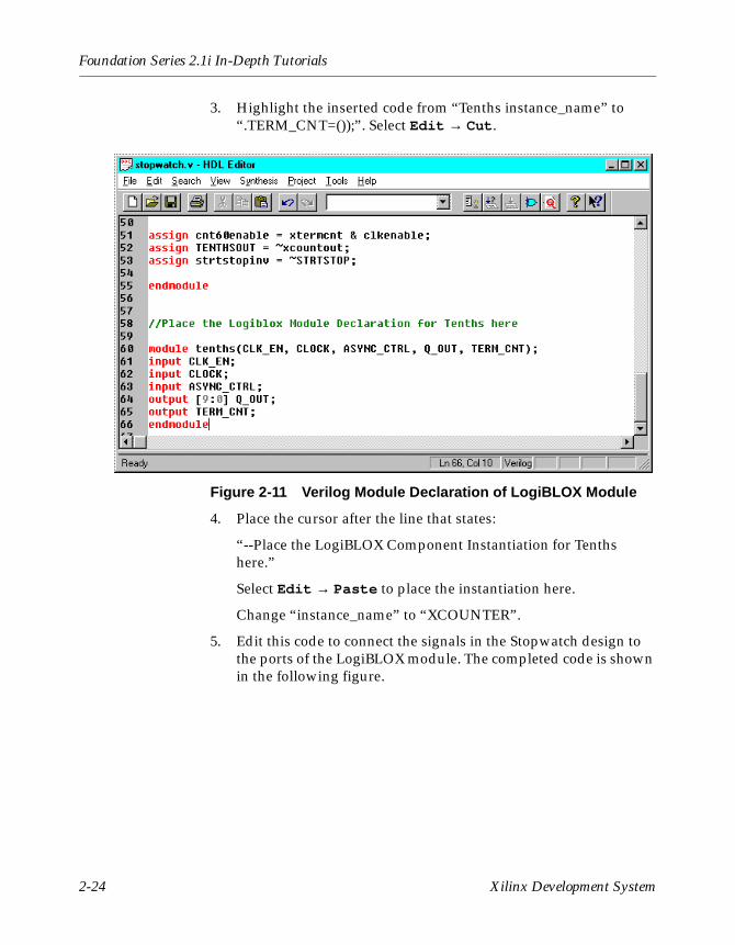
Foundation Series 2.1i In-Depth Tutorials
3. Highlight the inserted code from “Tenths instance_name” to “.TERM_CNT=());”. Select Edit → Cut.
Figure 2-11 Verilog Module Declaration of LogiBLOX Module
4. Place the cursor after the line that states:
“--Place the LogiBLOX Component Instantiation for Tenths here.”
Select Edit → Paste to place the instantiation here.
Change “instance_name” to “XCOUNTER”.
5. Edit this code to connect the signals in the Stopwatch design to the ports of the LogiBLOX module. The completed code is shown in the following figure.
2-24 Xilinx Development System
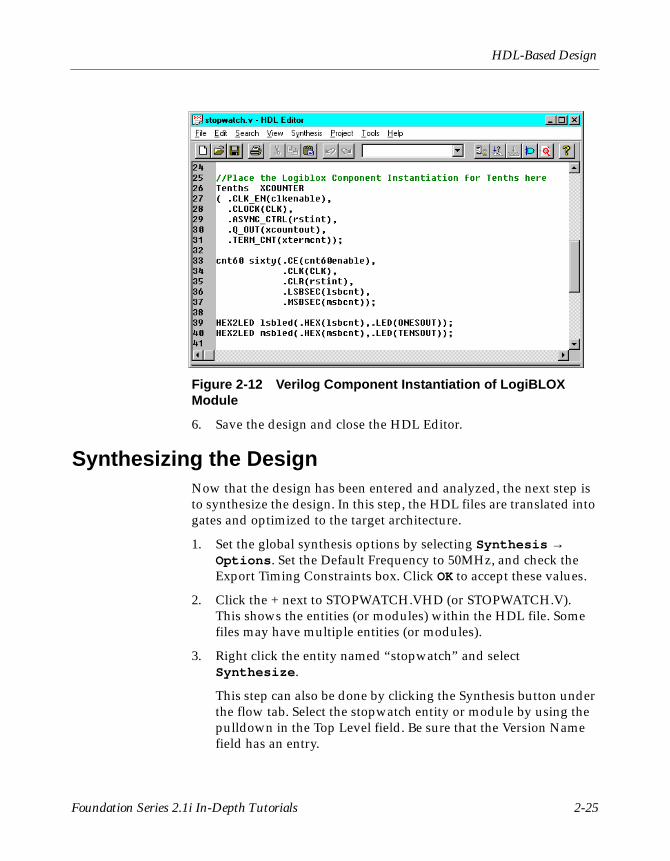
HDL-Based Design
Figure 2-12 Verilog Component Instantiation of LogiBLOX Module
6. Save the design and close the HDL Editor.
Synthesizing the DesignNow that the design has been entered and analyzed, the next step is to synthesize the design. In this step, the HDL files are translated into gates and optimized to the target architecture.
1. Set the global synthesis options by selecting Synthesis → Options. Set the Default Frequency to 50MHz, and check the Export Timing Constraints box. Click OK to accept these values.
2. Click the + next to STOPWATCH.VHD (or STOPWATCH.V). This shows the entities (or modules) within the HDL file. Some files may have multiple entities (or modules).
3. Right click the entity named “stopwatch” and select Synthesize.
This step can also be done by clicking the Synthesis button under the flow tab. Select the stopwatch entity or module by using the pulldown in the Top Level field. Be sure that the Version Name field has an entry.
Foundation Series 2.1i In-Depth Tutorials 2-25

Foundation Series 2.1i In-Depth Tutorials
4. Complete the Target Device fields with this information:
• Family: SpartanXL
• Device: S05XLPC84
• Speed Grade: -5
5. Check the boxes labeled Edit Synthesis/Implementation Constraints and View Estimated Performance after Optimization.
Selecting the Edit Synthesis/Implementation Constraints box automatically opens the Express Constraints Editor after synthesis is complete.
Selecting the View Estimated Performance after Optimization box automatically opens the Optimized dialog box which displays the results of the synthesis and optimization.
Figure 2-13 Synthesis/Implementation Window
6. Click Run. Express synthesizes the design and opens the Express Constraints Editor.
2-26 Xilinx Development System
HDL-Based Design
Note: The Express Constraints Editor is not available to non-registered users or with Base Express licenses. All the functionality covered by the Express Constraints Editor can be achieved by component instantiation (Pullups, Pulldowns, Clock Buffers, I/O Flip Flops), UCF file (timing constraints, pin location constraints), or MAP options (merging flip flops into IOBs). If you are a Base Express customer, skip to the “Functional Simulation” chapter.
The Express Constraints Editor (Foundation Express Only)
You control optimization options and pass timing specifications to the Place and Route software through a GUI in the Express Synthesis software. This editor is only available with the Foundation Express product not Base Express. All timing specifications are passed in the netlist directly to the place and route engine and are used in the synthesis process for timing estimation purposes only.
• Clocks
The Default Frequency set in Synthesis → Options is applied to all clocks in the design. To change the specification of a clock, click inside the box to the right of the clock and select Define. Enter the clock period or give the rise and fall times.
• Paths
All types of paths that can be covered by timing specifications are listed here, with unique specifications given for each clock in the design. To modify these specifications, enter a new delay in the Req. Delay column.
To create a subpath within a path, right click the source or destination and select New Subpath. Give the subpath a new name and delay value, then select sources and destinations by double clicking the instances. You can also use wildcards in the selection filters to choose a group of elements.
Foundation Series 2.1i In-Depth Tutorials 2-27
Foundation Series 2.1i In-Depth Tutorials
• Ports
With the Ports tab, you set input and out delay requirements, assign clock buffers, insert pullup or pulldown resistors in the I/O, set delay properties for input registers, set slew rate, disable the use of I/O registers, and assign pin locations. For all but the pin locations, click in the box to use the pulldown menu. For pin locations, type the pin number in the box.
• Modules
With the Modules tab, you to keep or eliminate hierarchy and disable resource sharing. You can also override the default settings for effort and area versus speed at the module level.
• Xilinx Options
The Ignore unlinked cells during GSR mapping option directs Express to infer a global reset signal (and, therefore, insert the STARTUP module), even if black boxes have been instantiated. Express cannot know the reset characteristics of any logic in black boxes, so it will not insert STARTUP unless you check this option.
Using the Express Constraints Editor (Foundation Express Only)
Xilinx recommends that you let the automatic placement and routing program, PAR, define the pinout of your design. Pre-assigning locations to the pins can sometimes degrade the performance of the place-and-route tools. However, it is usually necessary, at some point, to lock the pinout of a design so that it can be integrated into a PCB (printed circuit board).
Define the initial pinout by running the place-and-route tools without pin assignments, then locking down the pin placement so that it reflects the locations chosen by the tools. Assign locations to the pins in the Watch design so that the design can function in a Xilinx demonstration board. Because the design is simple and timing is not critical, these pin assignments do not adversely affect the ability of PAR to place-and-route the design.
For HDL-based designs, these pin assignments can be done in a User Constraints File (.UCF) or with the Express Constraints Editor.
2-28 Xilinx Development System

HDL-Based Design
Although UCF files are provided for this tutorial, you will assign the pin location constraints in the Express Constraints Editor.
1. In the Express Constraint Editor, click the Import Constraints button. Select WATCHVHD.EXC or WATCHVER.EXC, depending on the language you are using. These files are located in the project directory.
This file has been created for you. The only difference you should see between your initial constraints and the ones saved in the .EXC file is the set of pin locations under the Ports tab.
You can save Constraint Editor settings for a design by selecting File → Export Constraints. When this .EXC file is read in for a later synthesis run, all constraints are re-established in the GUI, as long as they can be matched to instances in the current version.
2. Under the Paths tab, click in the box in Row 2 below the Req. Delay header (from All Input Ports to RC-CLK). Change the delay to 15. Under the Ports tab, the Input Delays for RESET and STRTSTOP have changed to 15, as these represent all the Pad to Setup delays.
You can change the values of individual Input or Output Delays by clicking the value in the Ports tab and either editing the value there or using the pulldown tab to select a value or define a new one. Change the values on one of the output signals using one of these methods.
3. Under the Paths tab, right click either RC-CLK or All Output Ports in the third row and select New Subpath. The Create/Edit Timing Subpath window opens.
Give this new subpath a name, Sub_flops_to_out, and a Delay value, 18. On the left hand side, double click all four flip flops that contain the name /ver1/sixty/lsbcount/QOUT*, to determine the sources of this subpath. On the lower right hand side, use the filter to select the destinations. Type ONE* in the field and click the Select button. All the ports beginning with ONESOUT will be highlighted. Click OK to see your new subpath.
Foundation Series 2.1i In-Depth Tutorials 2-29

Foundation Series 2.1i In-Depth Tutorials
Note: Base Express users cannot access the Express Constraints Editor. Pin location constraints must therefore be defined in a UCF file, which Xilinx has provided. Select Implementation → Implementation Options. Click the Browse button next to User Constraints and select BASE.UCF.
Figure 2-14 Editing Subpath in the Express Constraints Editor
4. Under the Ports tab, add the three final pin locations in the Pad Loc column. Scroll to the right to see this column. CLK must be assigned to P13. RESET must be assigned to P28, and STRTSTOP must be assigned to P18. To reassign, click the box and enter the pin number (including the P).
Note: The remaining I/Os have pin assignments. This information is contained in the .exc file. which you imported in Step 1.
2-30 Xilinx Development System
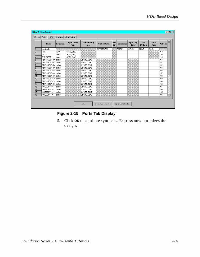
HDL-Based Design
Figure 2-15 Ports Tab Display
5. Click OK to continue synthesis. Express now optimizes the design.
Foundation Series 2.1i In-Depth Tutorials 2-31

Foundation Series 2.1i In-Depth Tutorials
Viewing Synthesis Results (Foundation Express Only)
With the View Estimated Performance after Optimization box checked, the Express Constraints Editor opens after the optimization phase of synthesis with preliminary performance results. The delay values are based on wireload models and, therefore, must be considered preliminary. Consult the post-route timing reports for the most accurate delay information.
1. Under the Clocks tab, examine the estimated delay value of the clock. Delays greater than the specification appear in red.
2. Under the Paths tab, examine the estimated delays for the paths and subpath. Click the source or destination of a path to see the members of the path, and click a specific path to see the individual segments of that path.
Figure 2-16 Estimated Timing Data Under Paths Tab
3. Examine the Ports tab to see that all of the settings and delays have been assigned and met.
2-32 Xilinx Development System

HDL-Based Design
4. Under the Modules tab, you can examine the elements used to synthesize this design. Click the box in the second row under Area and select Details. This section summarizes all the design elements used in the Stopwatch design that Express knows about.
Since the Tenths module is a LogiBLOX component and has not been synthesized by Express, it is UNLINKED and no summary information is available.
Note: Black boxes (modules not read into the Express design environment) are always noted as UNLINKED in the Express reports. As long as the underlying netlist (.xnf, .ngo, .ngc or EDIF) for a black box exists in the project directory, the Implementation tools merge the netlist in during the Translate phase. Since the Tenths module was built using LogiBLOX called from the project, the tenths NGC file will be found.
5. Click OK to complete the Synthesis phase.
At this point, an XNF file exists for the Stopwatch design. See the “Functional Simulation” chapter to perform a post-synthesis simulation of this design or refer to the “Design Implementation” chapter to place and route the design.
Foundation Series 2.1i In-Depth Tutorials 2-33

Foundation Series 2.1i In-Depth Tutorials
2-34 Xilinx Development System
Chapter 3
Functional Simulation
You can perform functional simulation before design implementation to verify that the logic that you have created is correct. Foundation provides a Logic Simulator, which is a gate-level simulator. You can perform functional simulation on a schematic-based design immediately after the design is captured in the Schematic Capture tool. In the case of an HDL-based design, you can perform functional simulation immediately following synthesis. In a later section, you can perform timing simulation, which takes place after the design is implemented (placed and routed) with the Xilinx Implementation Tools.
This chapter contains the following sections.
• “Starting the Logic Simulator”
• “Performing Simulation”
• “Adding Signals”
• “Adding Stimulus”
• “Running the Simulation”
• “Saving the Simulation”
Foundation Series 2.1i In-Depth Tutorials 3-1
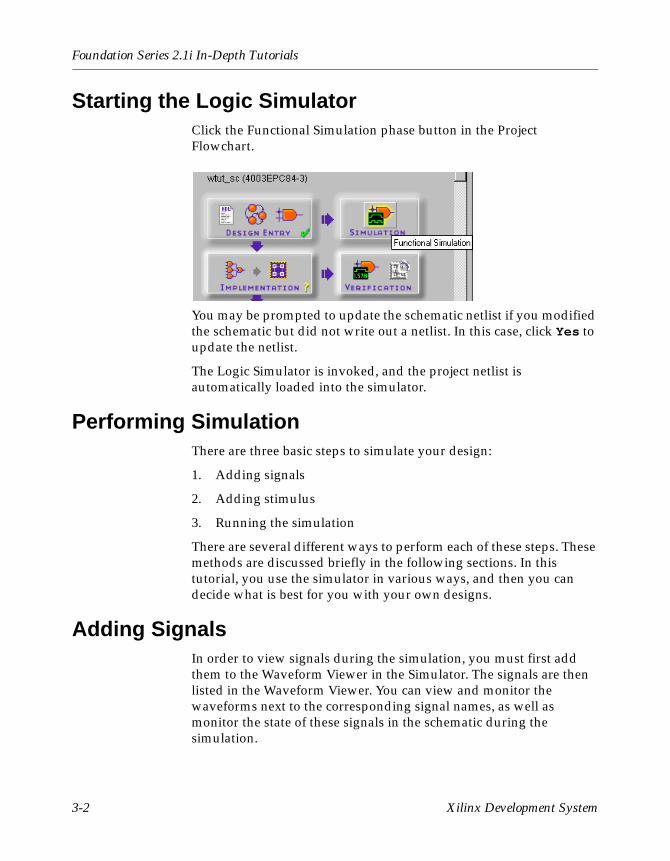
Foundation Series 2.1i In-Depth Tutorials
Starting the Logic SimulatorClick the Functional Simulation phase button in the Project Flowchart.
You may be prompted to update the schematic netlist if you modified the schematic but did not write out a netlist. In this case, click Yes to update the netlist.
The Logic Simulator is invoked, and the project netlist is automatically loaded into the simulator.
Performing SimulationThere are three basic steps to simulate your design:
1. Adding signals
2. Adding stimulus
3. Running the simulation
There are several different ways to perform each of these steps. These methods are discussed briefly in the following sections. In this tutorial, you use the simulator in various ways, and then you can decide what is best for you with your own designs.
Adding SignalsIn order to view signals during the simulation, you must first add them to the Waveform Viewer in the Simulator. The signals are then listed in the Waveform Viewer. You can view and monitor the waveforms next to the corresponding signal names, as well as monitor the state of these signals in the schematic during the simulation.
3-2 Xilinx Development System
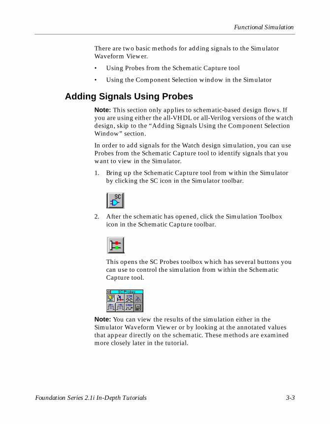
Functional Simulation
There are two basic methods for adding signals to the Simulator Waveform Viewer.
• Using Probes from the Schematic Capture tool
• Using the Component Selection window in the Simulator
Adding Signals Using ProbesNote: This section only applies to schematic-based design flows. If you are using either the all-VHDL or all-Verilog versions of the watch design, skip to the “Adding Signals Using the Component Selection Window” section.
In order to add signals for the Watch design simulation, you can use Probes from the Schematic Capture tool to identify signals that you want to view in the Simulator.
1. Bring up the Schematic Capture tool from within the Simulator by clicking the SC icon in the Simulator toolbar.
2. After the schematic has opened, click the Simulation Toolbox icon in the Schematic Capture toolbar.
This opens the SC Probes toolbox which has several buttons you can use to control the simulation from within the Schematic Capture tool.
Note: You can view the results of the simulation either in the Simulator Waveform Viewer or by looking at the annotated values that appear directly on the schematic. These methods are examined more closely later in the tutorial.
Foundation Series 2.1i In-Depth Tutorials 3-3
Foundation Series 2.1i In-Depth Tutorials
When the SC Probes toolbox is open, the cursor is automatically put into the Add Probes mode. You can see a probes icon attached to the cursor as shown in the following figure and the Add Probes button in the SC Probes toolbox is depressed. When you are adding probes to the schematic, you must remain in this Add Probes mode.
Figure 3-1 Cursor in Add Probes Mode
3. With the cursor in Add Probes mode, click once on the CLK signal name on the schematic. A gray box appears to the left of the CLK label. This gray box indicates that a probe has been attached to this signal.
4. Repeat Step 3 to add probes to the RESET and STRTSTOP signals and to the TENTHSOUT[9:0], ONESOUT[6:0] and TENSOUT[6:0] buses.
5. Return to the Simulator Waveform Viewer by clicking the SIM button in the SC Probes toolbox.
You should now see all of the signals you just probed listed in the Simulator Waveform Viewer.
3-4 Xilinx Development System
Functional Simulation
Figure 3-2 Simulator Signals List
Adding Signals Using the Component Selection Window
Follow these steps to add more signals using the Component Selection window within the Simulator.
1. Click the Component Selection icon in the toolbar in the Simulator or select Signal → Add Signals.
The Component Selection Window opens.
This window is divided into three panes. The left-most pane is the Signals Selection pane. This pane displays a list of all of the available signals for a given level of hierarchy. The middle pane, Chip Selection, displays a list of all of the components for a given level of hierarchy.
You can select a different level of hierarchy in the right-most pane entitled Scan Hierarchy. For instance, click the OUTS1 macro in the Scan Hierarchy pane. You are now looking at signals and components from the OUTS1 macro in the Signals Selection and Chip Selection panes, respectively.
Foundation Series 2.1i In-Depth Tutorials 3-5
Foundation Series 2.1i In-Depth Tutorials
Note: Because Express flattens the design during synthesis, you will only see this OUTS1 component with the schematic version of the design.
Figure 3-3 Scan Hierarchy Signals Selector
Return to the Root level of hierarchy by clicking the Hierarchy button and then selecting Root in the Scan Hierarchy pane to again view the signals from the top-level of the Watch design.
2. This step is divided into two parts, a) and b), for schematic-based design and HDL-based design, respectively.
a) Schematic-based design only
In the Signals Selection pane, several signals have red checkmarks next to their names. These signals have already been added to the Simulator, in this case by using probes in the Schematic Capture tool. Now you add more signals to the Waveform Viewer.
From the Signals Selection pane, you can either double click signals to add them to the Waveform Viewer, or you can single click and then press Add. Use whichever method you prefer to add the following buses.
ONES3, ONES0
TENS3, TENS0
3-6 Xilinx Development System
Functional Simulation
Note: It is possible to add these signals using probes on the schematic as you did for the other signals, but this process demonstrates the various methods for adding signals.
b) HDL-based design only
You add signals from the Signals Selection pane to the Waveform Viewer to view them during the simulation. From the Signals Selection pane, you can either double click signals to add them to the Waveform Viewer, or you may single click and then press Add. Use whichever method you prefer to add the following signals.
TENTHSOUT9, TENTHSOUT0
ONESOUT6, ONESOUT0
TENSOUT6, TENSOUT0
CLK
STRTSTOP
RESET
If you mistakenly add any signals you do not want to add, you double click them again in the Signals Selection pane to remove them from the Waveform Viewer. The red checkmark should then disappear.
3. Close the Component Selection window by clicking the Close button.
All of the signals you added are now shown in the Waveform Viewer.
Deleting a SignalTo delete any of the signals from the Waveform Viewer, first select the signal in the signal list in the Waveform Viewer, right-click, and then select Delete Signals → Selected. This operation removes the highlighted signal from the Waveform Viewer.
Foundation Series 2.1i In-Depth Tutorials 3-7
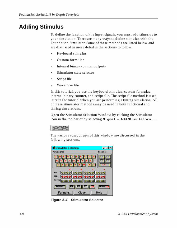
Foundation Series 2.1i In-Depth Tutorials
Adding StimulusTo define the function of the input signals, you must add stimulus to your simulation. There are many ways to define stimulus with the Foundation Simulator. Some of these methods are listed below and are discussed in more detail in the sections to follow.
• Keyboard stimulus
• Custom formulae
• Internal binary counter outputs
• Stimulator state selector
• Script file
• Waveform file
In this tutorial, you use the keyboard stimulus, custom formulae, internal binary counter, and script file. The script file method is used later in the tutorial when you are performing a timing simulation. All of these stimulator methods may be used in both functional and timing simulations.
Open the Stimulator Selection Window by clicking the Stimulator icon in the toolbar or by selecting Signal → Add Stimulators...
The various components of this window are discussed in the following sections.
Figure 3-4 Stimulator Selector
3-8 Xilinx Development System

Functional Simulation
Stimulating with the Internal Binary CounterThe Foundation Simulator includes an internal free-running 16-bit binary counter. You can use each of the 16 output bits of the counter as stimulators. These signals provide 50% duty cycle signals, each bit having half the frequency of the next least significant bit. These are useful when defining clock stimulus. You may define the frequency of the LSB of the counter (B0) and can therefore derive the frequen-cies of the other counter outputs.
These counter outputs are represented by the round yellow LEDs in the Stimulator Selection window. The row of red round LEDs below it represents the complement of the counter outputs. The B0 output (LSB) of the counter is the farthest LED to the right, and B15 (MSB) is all the way to the left.
To simulate the system clock, you assign stimulus to the CLK signal in the simulator. You use the B0 stimulator signal to stimulate the CLK signal in the Watch design.
1. In the Waveform Viewer, select the CLK signal by clicking it.
2. In the Stimulator Selection Window, click the B0 stimulator (the right-most yellow LED). You should now see a B0 next to the CLK signal in the Waveform Viewer indicating that the B0 stimulator is assigned to CLK.
3. Select Options → Preferences from the Simulator window. This opens the Preferences window. In the Simulation tab of this window, you can set the frequency of the B0 counter output.
4. Set the B0 frequency to 10MHz.
Foundation Series 2.1i In-Depth Tutorials 3-9

Foundation Series 2.1i In-Depth Tutorials
Figure 3-5 Simulator Preferences
5. Press OK to close the Preferences window.
Stimulating with Keyboard StimulatorsYou assign keyboard keys as stimulus for signals in your design with the keyboard in the Stimulator Selection window. After you assign this stimulus, the signal’s value toggles between 1 and 0 whenever you press the corresponding key on your PC’s keyboard. Additionally, you can assign a constant 1 or 0 to a signal using the 1 and 0 keys on the Stimulator Selector’s keyboard.
Now assign the R keyboard stimulus to the RESET signal in the Watch design.
1. Click and drag the R key on the keyboard in the Stimulator Selector onto the RESET signal name in the Waveform Viewer.
You should now see an R next to the RESET signal in the Wave-form Viewer, which indicates that this is the assigned stimulus.
2. Press the R key on your PC keyboard a few times to see the state of the stimulus changing in the Waveform Viewer.
Stimulating with Custom FormulaeThe 16 square LEDs in the Stimulator Selector represent Custom Formulae. You have the option to define each of these 16 formulae to any custom stimulus pattern you want.
3-10 Xilinx Development System
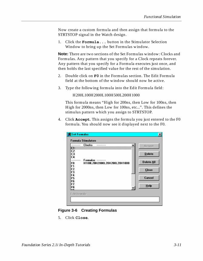
Functional Simulation
Now create a custom formula and then assign that formula to the STRTSTOP signal in the Watch design.
1. Click the Formula... button in the Stimulator Selection Window to bring up the Set Formulas window.
Note: There are two sections of the Set Formulas window: Clocks and Formulas. Any pattern that you specify for a Clock repeats forever. Any pattern that you specify for a Formula executes just once, and then holds the last specified value for the rest of the simulation.
2. Double click on F0 in the Formulas section. The Edit Formula field at the bottom of the window should now be active.
3. Type the following formula into the Edit Formula field:
H200L100H2000L100H500L200H1000
This formula means “High for 200ns, then Low for 100ns, then High for 2000ns, then Low for 100ns, etc...”. This defines the stimulus pattern which you assign to STRTSTOP.
4. Click Accept. This assigns the formula you just entered to the F0 formula. You should now see it displayed next to the F0.
Figure 3-6 Creating Formulas
5. Click Close.
Foundation Series 2.1i In-Depth Tutorials 3-11
Foundation Series 2.1i In-Depth Tutorials
6. Assign this newly created F0 formula to the STRTSTOP signal. Click the F0 LED in the Stimulator Selection box (the farthest square LED to the right) and drag it onto the STRTSTOP signal in the Waveform Viewer. You should now see an F0 next to the STRTSTOP signal indicating that the F0 formula has been assigned as stimulus for that signal. The F0 formula may now also be used for any other signals you want within this same project.
Other Sections of the Stimulator SelectorThere are a few more sections of the Stimulator Selector that are not used in this tutorial, but are discussed briefly here. For complete documentation on these topics, refer to the Foundation Logic Simulator online help.
The Clocks section contains four custom clock signals. These custom clocks are defined in the Set Formulas window as mentioned above in the Custom Formula section. These custom clocks are useful for clocks with duty cycles other than 50%. You could not use the internal binary counter outputs for those types of clocks or for other repeating functions.
The EN, DS, CC, OV, and CS buttons pertain to the “mode” of the signal and stimulus. These modes control options, such as whether the stimulus is overridden by internally driven signals and whether the stimulus is enabled or disabled at a given time.
Finally, the Delete button deletes the stimulus from a selected signal. This function does not delete the signal from the waveform viewer. It merely deletes the stimulus associated with that signal.
Close the Stimulator Selection window by clicking Close.
Running the SimulationNow you should see the three inputs of the Watch design, CLK, RESET, and STRTSTOP listed in the Waveform Viewer, each having some type of stimulus associated with it. You should also see the outputs TENTHSOUT, TENSOUT, ONESOUT, ONES, and TENS listed (ONES and TENS will only be visible for the schematic-based designs). You are now ready to run the simulation.
3-12 Xilinx Development System
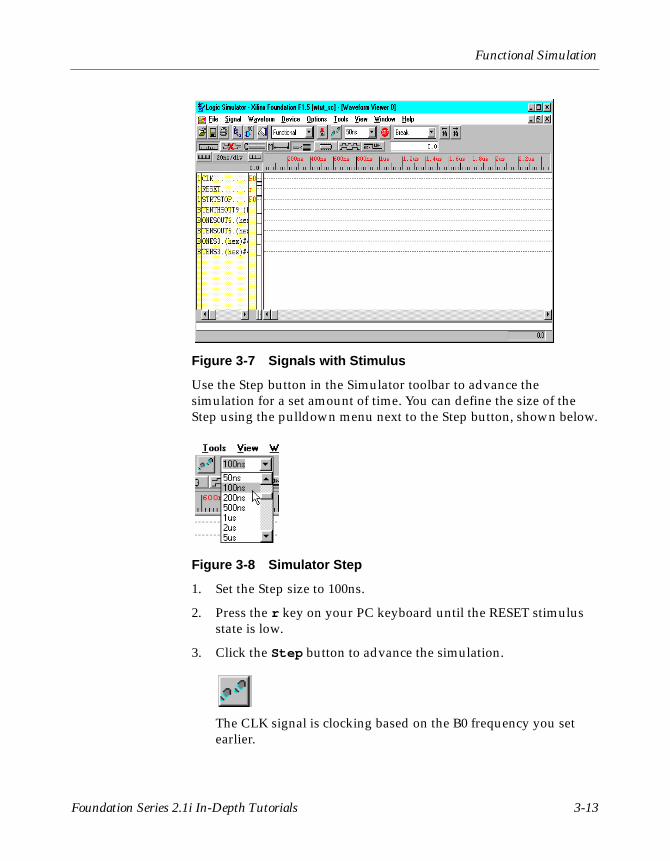
Functional Simulation
Figure 3-7 Signals with Stimulus
Use the Step button in the Simulator toolbar to advance the simulation for a set amount of time. You can define the size of the Step using the pulldown menu next to the Step button, shown below.
Figure 3-8 Simulator Step
1. Set the Step size to 100ns.
2. Press the r key on your PC keyboard until the RESET stimulus state is low.
3. Click the Step button to advance the simulation.
The CLK signal is clocking based on the B0 frequency you set earlier.
Foundation Series 2.1i In-Depth Tutorials 3-13

Foundation Series 2.1i In-Depth Tutorials
The STRTSTOP signal follows the formula created earlier.
4. Continue to click the Step button to advance the simulation.
Does the circuit appear to be working properly? Is the stopwatch counting? Remember that the tenths digit is a one-hot encoded value. To better see the results, you can change the radix of this bus to binary by first clicking the TENTHSOUT bus, right-clicking and selecting Bus → Display → Binary. You may also change the scale of the Waveform Viewer by clicking on the Scale buttons.
Recall that the ONESOUT and TENSOUT buses are in 7-segment display format, so the value of the bus may not be readily clear. Below is a diagram of the layout of the 7-segment display to help with verification.
Figure 3-9 7-Segment Display
If the design is schematic-based, you can view a model of the 7-segment display on the schematic, as described below, for easier debugging. With a schematic-based design, you are also viewing the ONES and TENS bus in the Waveform viewer. These buses are the 4-bit binary values of the ones and tens digits. To better see these values, you can change the radix of the buses. by clicking the ONES bus, right-clicking and selecting Bus → Display → Decimal. Repeat this procedure for the TENS bus.
X8774
0
6
4 2
3
15
Decimal point
3-14 Xilinx Development System
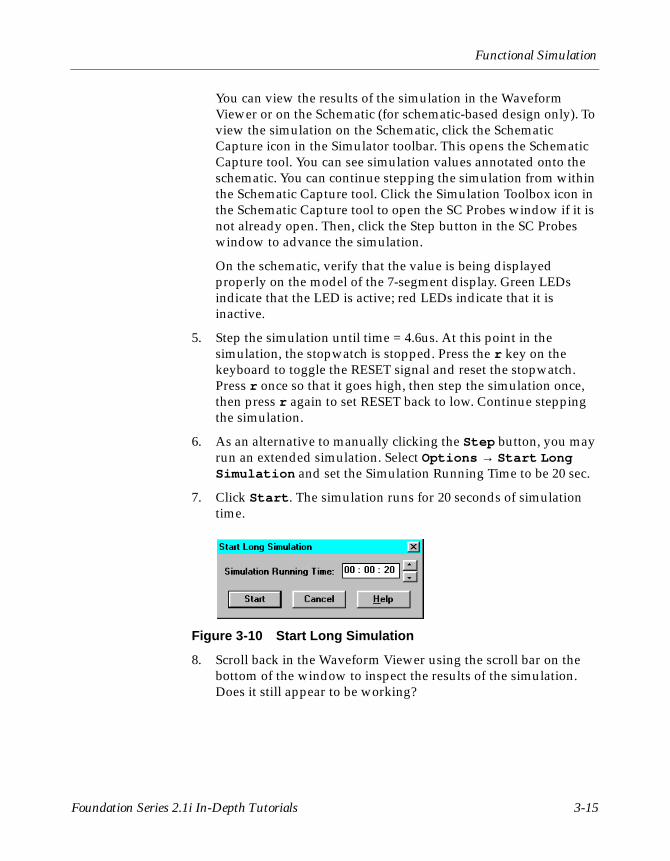
Functional Simulation
You can view the results of the simulation in the Waveform Viewer or on the Schematic (for schematic-based design only). To view the simulation on the Schematic, click the Schematic Capture icon in the Simulator toolbar. This opens the Schematic Capture tool. You can see simulation values annotated onto the schematic. You can continue stepping the simulation from within the Schematic Capture tool. Click the Simulation Toolbox icon in the Schematic Capture tool to open the SC Probes window if it is not already open. Then, click the Step button in the SC Probes window to advance the simulation.
On the schematic, verify that the value is being displayed properly on the model of the 7-segment display. Green LEDs indicate that the LED is active; red LEDs indicate that it is inactive.
5. Step the simulation until time = 4.6us. At this point in the simulation, the stopwatch is stopped. Press the r key on the keyboard to toggle the RESET signal and reset the stopwatch. Press r once so that it goes high, then step the simulation once, then press r again to set RESET back to low. Continue stepping the simulation.
6. As an alternative to manually clicking the Step button, you may run an extended simulation. Select Options → Start Long Simulation and set the Simulation Running Time to be 20 sec.
7. Click Start. The simulation runs for 20 seconds of simulation time.
Figure 3-10 Start Long Simulation
8. Scroll back in the Waveform Viewer using the scroll bar on the bottom of the window to inspect the results of the simulation. Does it still appear to be working?
Foundation Series 2.1i In-Depth Tutorials 3-15

Foundation Series 2.1i In-Depth Tutorials
Saving the SimulationAfter you run a simulation, you can save it for future use. You can save the Waveforms you captured as test vectors, and then load them into the simulator to use again later.
1. Select File → Save Waveform. In the dialog box that opens, you can enter a name for the waveform file (.TVE). You can choose any name and save the waveform file.
You can load this waveform file into the simulator using the File → Load Waveform command.
2. Close the Simulator.
3-16 Xilinx Development System
Chapter 4
Design Implementation
Design Implementation is the process of translating, mapping, placing, routing, and generating a BIT file for your design. The Design Implementation tools are embedded into the Foundation Project Manager for easy access and project management.
This chapter contains the following sections.
• “Project Management”
• “Starting Implementation”
• “Implementation Options”
• “Running Implementation — The Flow Engine”
• “Viewing Implementation Results”
• “Other Implementation Tools”
Project ManagementProject management controls design versions and revisions. A version represents an input design netlist. Each time a change is made to the source design, such as logic being added to or removed from the schematic or the HDL source being modified, a new version is created. A revision represents an implementation on a given version, usually with new implementation options, such as different placement or router effort level.
Foundation maintains revision control, meaning that the resulting files from each implementation revision are archived in the project directory.
Foundation Series 2.1i In-Depth Tutorials 4-1

Foundation Series 2.1i In-Depth Tutorials
Note: In 2.1i, you can archive an entire project, design source files, synthesis files, and implementation files.
Foundation manages and displays your design versions and revisions graphically in the Versions tab of the Project Manager. Since you have not yet implemented the design, the Versions tab is currently empty.
Starting ImplementationThis section describes how to begin implementation depending on which tutorial you performed: HDL or schematic.
• If you performed the schematic tutorial, proceed to the “Implementing the Schematic Design” section.
• If you performed the HDL tutorial, proceed to the “Implementing the HDL Design” section.
Implementing the Schematic DesignTo begin implementation of your schematic design, click the Implementation phase button in the Project Flow diagram.
If you are asked if you wish to update the EDIF netlist because the schematic is newer, say Yes to update the EDIF netlist. This EDIF netlist is the actual input file to the Design Implementation tools.
Next you will see the Implement Design dialog box.
4-2 Xilinx Development System
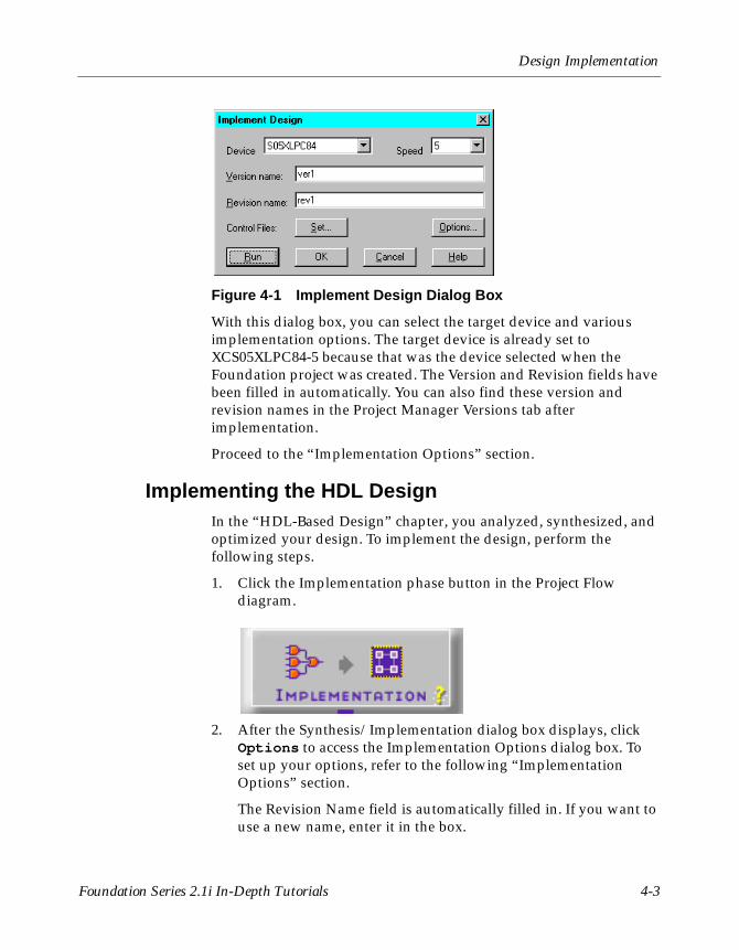
Design Implementation
Figure 4-1 Implement Design Dialog Box
With this dialog box, you can select the target device and various implementation options. The target device is already set to XCS05XLPC84-5 because that was the device selected when the Foundation project was created. The Version and Revision fields have been filled in automatically. You can also find these version and revision names in the Project Manager Versions tab after implementation.
Proceed to the “Implementation Options” section.
Implementing the HDL DesignIn the “HDL-Based Design” chapter, you analyzed, synthesized, and optimized your design. To implement the design, perform the following steps.
1. Click the Implementation phase button in the Project Flow diagram.
2. After the Synthesis/Implementation dialog box displays, click Options to access the Implementation Options dialog box. To set up your options, refer to the following “Implementation Options” section.
The Revision Name field is automatically filled in. If you want to use a new name, enter it in the box.
Foundation Series 2.1i In-Depth Tutorials 4-3

Foundation Series 2.1i In-Depth Tutorials
Figure 4-2 Synthesis/Implementation Dialog Box
4-4 Xilinx Development System

Design Implementation
Implementation OptionsClick the Options button. The Options dialog box opens. A summary of the options provided in this box follows.
Figure 4-3 Implementation Options Dialog Box
• Place and Route Effort level slider bar. Use this slider bar to select the amount of time and effort the tools spend implementing the design.
• Program Option Templates. You can access various implementation, simulation, and configuration options. For this design, make sure that “Foundation EDIF” is selected for Simulation and “Default” for Implementation and Configuration. Either of these two templates can be set to Off if you do not wish these output files to be created. See the next section for a description of the Implementation template.
See the Design Manager/Flow Engine Guide for more details about these optional target settings.
Foundation Series 2.1i In-Depth Tutorials 4-5
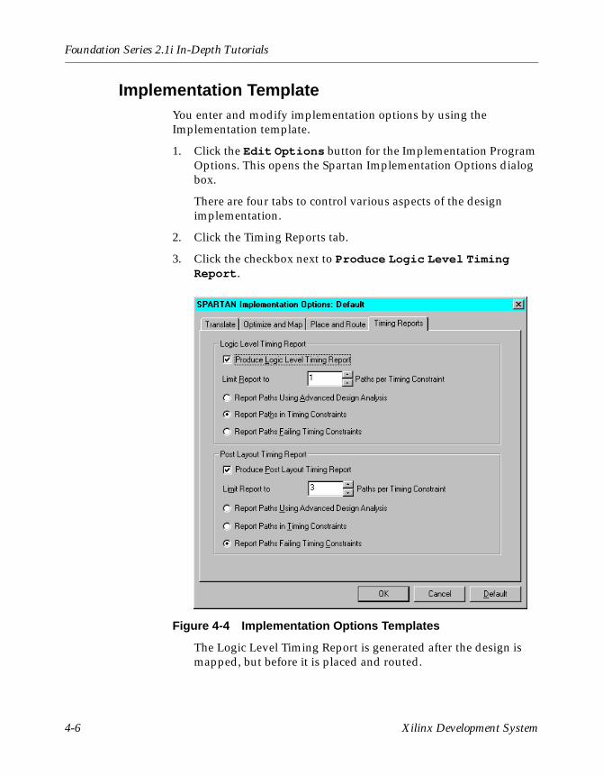
Foundation Series 2.1i In-Depth Tutorials
Implementation TemplateYou enter and modify implementation options by using the Implementation template.
1. Click the Edit Options button for the Implementation Program Options. This opens the Spartan Implementation Options dialog box.
There are four tabs to control various aspects of the design implementation.
2. Click the Timing Reports tab.
3. Click the checkbox next to Produce Logic Level Timing Report.
Figure 4-4 Implementation Options Templates
The Logic Level Timing Report is generated after the design is mapped, but before it is placed and routed.
4-6 Xilinx Development System
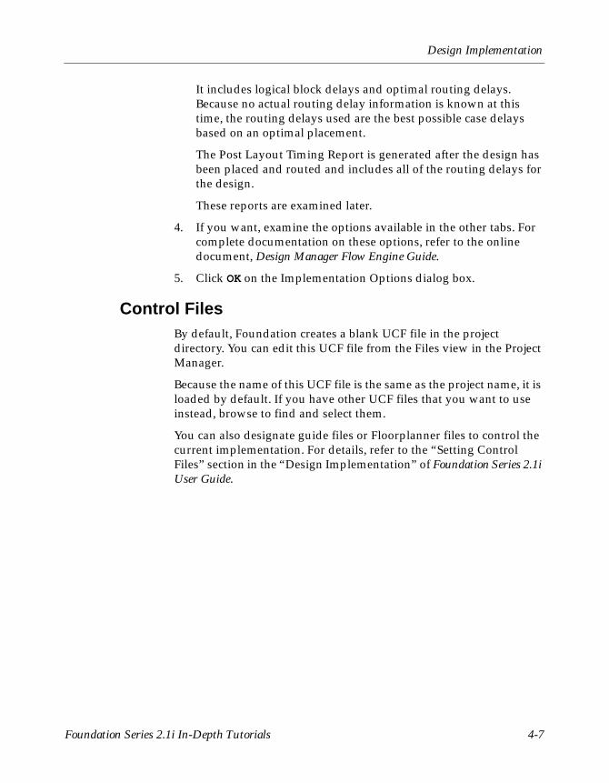
Design Implementation
It includes logical block delays and optimal routing delays. Because no actual routing delay information is known at this time, the routing delays used are the best possible case delays based on an optimal placement.
The Post Layout Timing Report is generated after the design has been placed and routed and includes all of the routing delays for the design.
These reports are examined later.
4. If you want, examine the options available in the other tabs. For complete documentation on these options, refer to the online document, Design Manager Flow Engine Guide.
5. Click OK on the Implementation Options dialog box.
Control FilesBy default, Foundation creates a blank UCF file in the project directory. You can edit this UCF file from the Files view in the Project Manager.
Because the name of this UCF file is the same as the project name, it is loaded by default. If you have other UCF files that you want to use instead, browse to find and select them.
You can also designate guide files or Floorplanner files to control the current implementation. For details, refer to the “Setting Control Files” section in the “Design Implementation” of Foundation Series 2.1i User Guide.
Foundation Series 2.1i In-Depth Tutorials 4-7
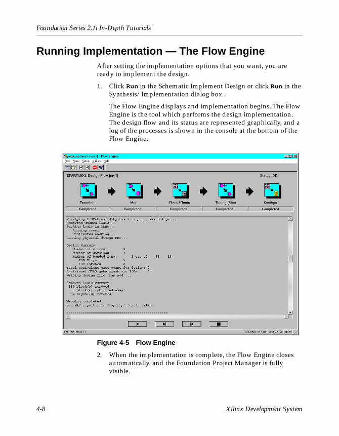
Foundation Series 2.1i In-Depth Tutorials
Running Implementation — The Flow EngineAfter setting the implementation options that you want, you are ready to implement the design.
1. Click Run in the Schematic Implement Design or click Run in the Synthesis/Implementation dialog box.
The Flow Engine displays and implementation begins. The Flow Engine is the tool which performs the design implementation. The design flow and its status are represented graphically, and a log of the processes is shown in the console at the bottom of the Flow Engine.
Figure 4-5 Flow Engine
2. When the implementation is complete, the Flow Engine closes automatically, and the Foundation Project Manager is fully visible.
4-8 Xilinx Development System
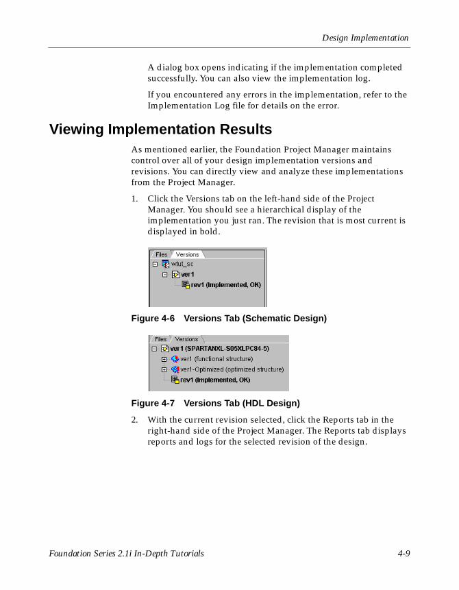
Design Implementation
A dialog box opens indicating if the implementation completed successfully. You can also view the implementation log.
If you encountered any errors in the implementation, refer to the Implementation Log file for details on the error.
Viewing Implementation ResultsAs mentioned earlier, the Foundation Project Manager maintains control over all of your design implementation versions and revisions. You can directly view and analyze these implementations from the Project Manager.
1. Click the Versions tab on the left-hand side of the Project Manager. You should see a hierarchical display of the implementation you just ran. The revision that is most current is displayed in bold.
Figure 4-6 Versions Tab (Schematic Design)
Figure 4-7 Versions Tab (HDL Design)
2. With the current revision selected, click the Reports tab in the right-hand side of the Project Manager. The Reports tab displays reports and logs for the selected revision of the design.
Foundation Series 2.1i In-Depth Tutorials 4-9
Foundation Series 2.1i In-Depth Tutorials
3. Double click the report entitled Implementation Report Files. This displays the Xilinx Report Browser, which contains all of the implementation reports. You have the option to browse through any of these reports at this time.
4. From within the Xilinx Report Browser, double click the Logic Level Timing Report. Inspect this report to find the maximum system frequency specified. Remember this frequency.
5. Again, from within the Xilinx Report Browser, double click the Post-Layout Timing Report. Inspect this report to find what the maximum frequency is. Compare this with the delay you found in the Logic Level Timing Report.
The difference in the two reports’ delays can be accounted for by the actual routing delays. The routing delays which are assumed in the Logic Level Timing Report are best-case, which is why they are generally smaller than the actual delays after placement and routing. Logic Level timing is useful because it gives you a preliminary look at how realistic your timing goals are, given the design’s current mapped state.
A rough guideline (known as the 50/50 rule) is that the logical block delays in any particular path will make up about 50% of the total path delay once the design is routed. This is, of course, just a guideline, and designs vary from case to case. But, this gives you some estimate to determine whether the design’s timing is even close to your goals before the design is completely placed and routed.
6. After you have perused the timing reports, close the reports and close the Report Browser.
7. Return to the Flow tab on the right-hand side of the Project Manager by clicking on it.
4-10 Xilinx Development System

Design Implementation
Other Implementation ToolsThe Foundation Project Manager also gives you access to the other implementation tools, including the Timing Analyzer, FPGA Editor, Floorplanner, JTAG Programmer, Prom File Formatter and Hardware Debugger. These tools can be invoked from the Tools → Implementation and Tools → Device Programming menus. The Timing Analyzer and Device Programming tools are also available from the Flow diagram.
These implementation tools are sensitive to the implementation revision. In other words, depending on which Revision you have selected in the Versions tab when you invoke the tool, it will load the tool with data from that implementation revision.
Now you can invoke any of these tools to see what they look like. For more information on using these tools, refer to the appropriate online documentation for each tool.
Foundation Series 2.1i In-Depth Tutorials 4-11

Foundation Series 2.1i In-Depth Tutorials
4-12 Xilinx Development System
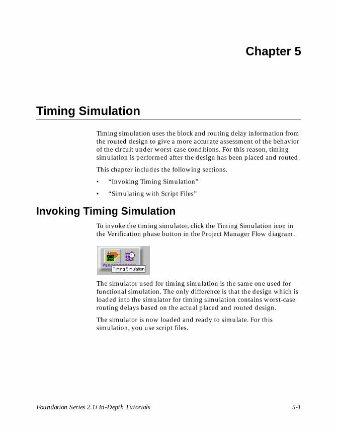
Chapter 5
Timing Simulation
Timing simulation uses the block and routing delay information from the routed design to give a more accurate assessment of the behavior of the circuit under worst-case conditions. For this reason, timing simulation is performed after the design has been placed and routed.
This chapter includes the following sections.
• “Invoking Timing Simulation”
• “Simulating with Script Files”
Invoking Timing SimulationTo invoke the timing simulator, click the Timing Simulation icon in the Verification phase button in the Project Manager Flow diagram.
The simulator used for timing simulation is the same one used for functional simulation. The only difference is that the design which is loaded into the simulator for timing simulation contains worst-case routing delays based on the actual placed and routed design.
The simulator is now loaded and ready to simulate. For this simulation, you use script files.
Foundation Series 2.1i In-Depth Tutorials 5-1
Foundation Series 2.1i In-Depth Tutorials
Simulating with Script FilesIn the “Functional Simulation” chapter, you simulated by applying various types of stimulus including keyboard stimulus, formulae, and by using the internal binary counter. In this chapter, you use a script file to simulate the design.
Script files contain commands to stimulate inputs, display signals, and advance the simulation. You enter your commands in the script file and then press one button to run the entire simulation. Script files in Foundation support Viewlogic-style commands, as well as other Foundation-specific commands. The Simulator Online Help provides a full list and description of all the supported commands.
Creating Script Files — Script Wizard and Script Editor
The Script Editor is a text editor that you use to enter, edit, and view script files, as well as actually run the simulation. You may either create a script file from scratch, use an existing one, or create one with the help of the Script Wizard, an interactive tool which helps you create script files for simulation. In this section, you use the Script Wizard to create a complete script file to simulate the Watch design and then view the script file and run the simulation from the Script Editor.
1. To invoke the Script Editor, select Tools → Script Editor from the pulldown menus within the Simulator. A dialog box prompts you to select a script file.
2. Choose Use Script Wizard to invoke the Script Wizard.
3. Follow the instructions in the Wizard to advance to the Initialization page.
4. On the Initialization page, select the following options.
5-2 Xilinx Development System
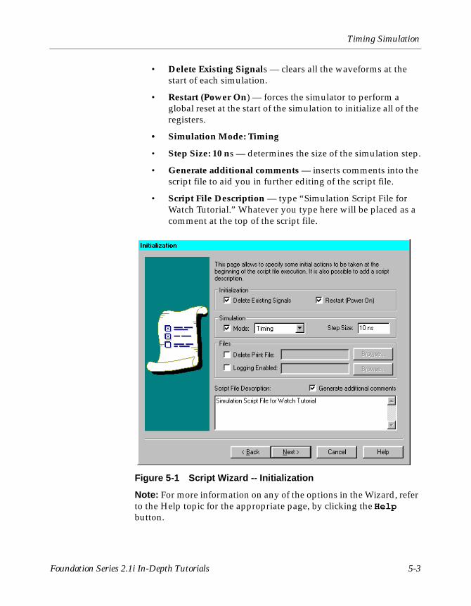
Timing Simulation
• Delete Existing Signals — clears all the waveforms at the start of each simulation.
• Restart (Power On) — forces the simulator to perform a global reset at the start of the simulation to initialize all of the registers.
• Simulation Mode: Timing
• Step Size: 10 ns — determines the size of the simulation step.
• Generate additional comments — inserts comments into the script file to aid you in further editing of the script file.
• Script File Description — type “Simulation Script File for Watch Tutorial.” Whatever you type here will be placed as a comment at the top of the script file.
Figure 5-1 Script Wizard -- Initialization
Note: For more information on any of the options in the Wizard, refer to the Help topic for the appropriate page, by clicking the Help button.
Foundation Series 2.1i In-Depth Tutorials 5-3

Foundation Series 2.1i In-Depth Tutorials
5. Click Next to advance to the Vectors page.
Vectors provide a more convenient way to use buses in the script file. By defining vectors, you can more easily refer to these buses in the rest of the script file. You can also create vectors out of any group of signals, regardless of whether they are a bus in the original design.
In this step, you define vectors for the three output buses, ONESOUT[6:0], TENSOUT[6:0], and TENTHSOUT[9:0]. For simplicity, name these vectors ONES, TENS and TENTHS, respectively.
6. Click the New button. This adds a new vector to the vector list entitled Vector_Name_1 by default. Type TENS in the place of Vector_Name_1 to rename it.
7. Click the Browse... button. This displays a Component Selection window which contains all of the signals in the design. On the right-hand side, scroll down to find the TENOUTS6..0 7-bit bus. Select this bus, and then click OK. By doing this, you have assigned the seven bits of the TENSOUT bus to the newly created TENS vector.
Figure 5-2 Script Wizard Component Selection
The seven bits of the TENSOUT bus are listed as components in the newly created TENS vector.
5-4 Xilinx Development System
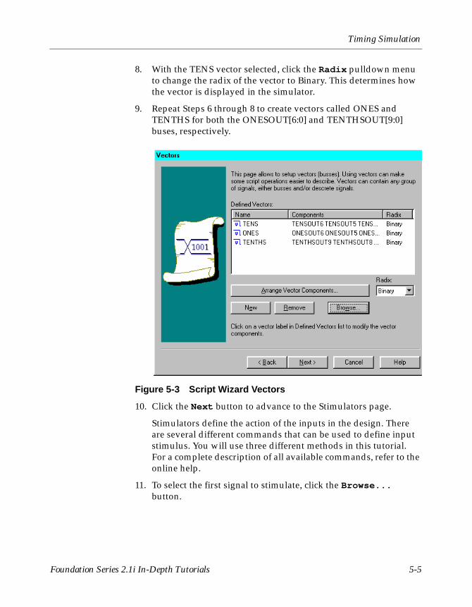
Timing Simulation
8. With the TENS vector selected, click the Radix pulldown menu to change the radix of the vector to Binary. This determines how the vector is displayed in the simulator.
9. Repeat Steps 6 through 8 to create vectors called ONES and TENTHS for both the ONESOUT[6:0] and TENTHSOUT[9:0] buses, respectively.
Figure 5-3 Script Wizard Vectors
10. Click the Next button to advance to the Stimulators page.
Stimulators define the action of the inputs in the design. There are several different commands that can be used to define input stimulus. You will use three different methods in this tutorial. For a complete description of all available commands, refer to the online help.
11. To select the first signal to stimulate, click the Browse... button.
Foundation Series 2.1i In-Depth Tutorials 5-5
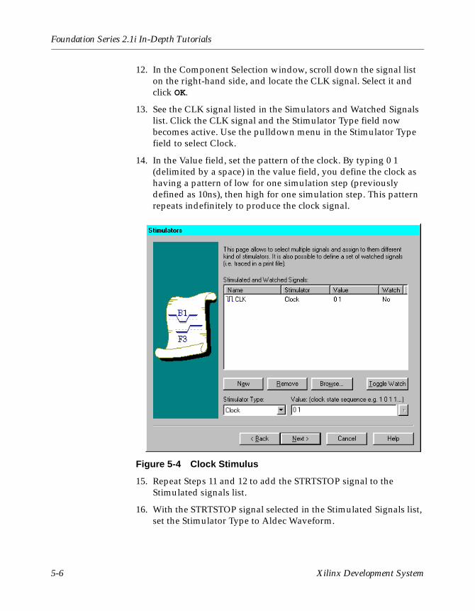
Foundation Series 2.1i In-Depth Tutorials
12. In the Component Selection window, scroll down the signal list on the right-hand side, and locate the CLK signal. Select it and click OK.
13. See the CLK signal listed in the Simulators and Watched Signals list. Click the CLK signal and the Stimulator Type field now becomes active. Use the pulldown menu in the Stimulator Type field to select Clock.
14. In the Value field, set the pattern of the clock. By typing 0 1 (delimited by a space) in the value field, you define the clock as having a pattern of low for one simulation step (previously defined as 10ns), then high for one simulation step. This pattern repeats indefinitely to produce the clock signal.
Figure 5-4 Clock Stimulus
15. Repeat Steps 11 and 12 to add the STRTSTOP signal to the Stimulated signals list.
16. With the STRTSTOP signal selected in the Stimulated Signals list, set the Stimulator Type to Aldec Waveform.
5-6 Xilinx Development System

Timing Simulation
17. In the Value field, type the following:
H200L100H2000L100H500L200H1000
Similar to the Custom Formula you created in the Functional Simulation section, this waveform means high for 200ns, then low for 100ns, then high for 200ns, and so on. This waveform will define a stimulus pattern for the STRTSTOP input signal.
18. Repeat Steps 11 through 12 to add the RESET signal to the Stimulated Signals list.
19. With the RESET signal selected in the Stimulated Signals list, set the Stimulator Type to be Waveform.
20. In the value field type the following.
@0=0 6500=1 400=0
This means “at 0ns the signal is 0, 650ns later the signal is high, 40ns later the signal is low.” Note that the units of this measurement are tenths of nanoseconds. This waveform provides a reset pulse to reset the stopwatch during the simulation.
21. The Stimulators page also allows you to select signals which you wish to “watch” in a printed output file. Since you will be setting a printed output file in the next section of the Wizard, you will add more signals to this list so that they may be watched.
Repeat Steps 11 and 12 to add the TENS, ONES, and TENTHS vectors to the Stimulated and Watched Signals list. Be sure that you add the vectors and not the buses.
Foundation Series 2.1i In-Depth Tutorials 5-7
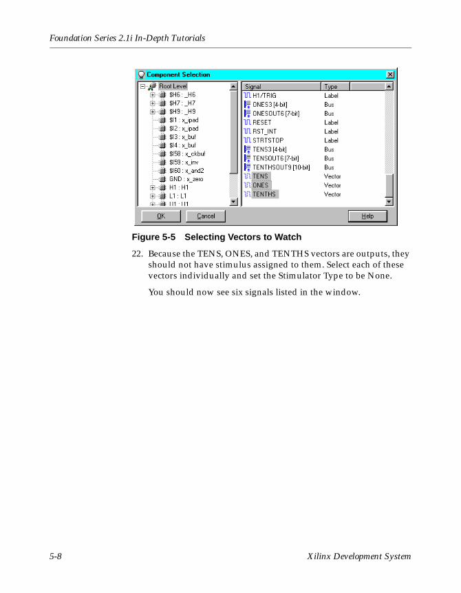
Foundation Series 2.1i In-Depth Tutorials
Figure 5-5 Selecting Vectors to Watch
22. Because the TENS, ONES, and TENTHS vectors are outputs, they should not have stimulus assigned to them. Select each of these vectors individually and set the Stimulator Type to be None.
You should now see six signals listed in the window.
5-8 Xilinx Development System

Timing Simulation
Figure 5-6 Signals’ Stimulus
23. Click Next to advance to the Breakpoints and Simulation page.
24. Breakpoints allow you to monitor the simulation for some output response. You can specify how the simulator will notify you when the output response is detected.
On the Breakpoints and Simulation page, click the Browse... button to choose the first signal to set a breakpoint on.
25. In the Component Selection window, choose the ONES vector from the signal list and click OK.
26. You should now see the ONES vector listed in the Defined Breakpoints list. Highlight ONES, and then from the Condition pulldown menu, select Low State. This defines the condition which must be present on the ONES vector for the breakpoint to occur.
27. In the Action field, type the following:
print > tim_out.txt
Foundation Series 2.1i In-Depth Tutorials 5-9
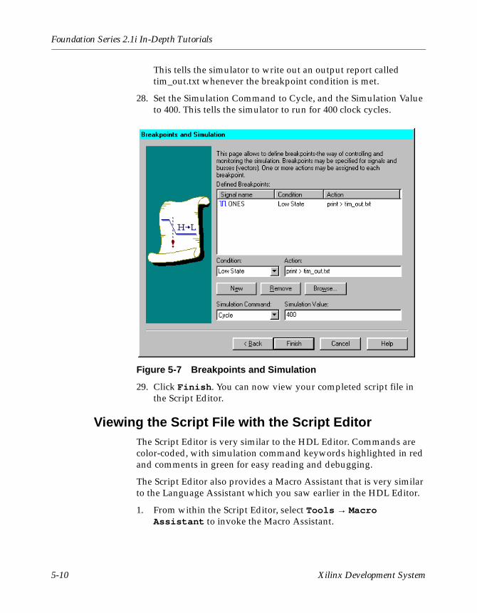
Foundation Series 2.1i In-Depth Tutorials
This tells the simulator to write out an output report called tim_out.txt whenever the breakpoint condition is met.
28. Set the Simulation Command to Cycle, and the Simulation Value to 400. This tells the simulator to run for 400 clock cycles.
Figure 5-7 Breakpoints and Simulation
29. Click Finish. You can now view your completed script file in the Script Editor.
Viewing the Script File with the Script EditorThe Script Editor is very similar to the HDL Editor. Commands are color-coded, with simulation command keywords highlighted in red and comments in green for easy reading and debugging.
The Script Editor also provides a Macro Assistant that is very similar to the Language Assistant which you saw earlier in the HDL Editor.
1. From within the Script Editor, select Tools → Macro Assistant to invoke the Macro Assistant.
5-10 Xilinx Development System

Timing Simulation
The Macro Assistant provides templates and help for the various script file commands. Browse through the various templates to see what is available.
Figure 5-8 Macro Assistant
2. Close the Macro Assistant by clicking the X in the upper-right corner of the window.
3. Save the script file that was created by the Script Wizard by selecting File → Save. Be sure that the file is being saved into the current Foundation project directory (that is, C:\FNDTN\ACTIVE\PROJECTS\watch_proj_name). Name the script file watchtim.cmd.
4. Look through the script file to see what the Script Wizard created.
Running the Simulation from the Script Editor1. You can execute the simulation directly from the Script Editor. To
do this, select Execute → Go.
A log of the executed commands appears at the bottom of the Script Editor, including messages indicating when breakpoints were encountered.
Foundation Series 2.1i In-Depth Tutorials 5-11
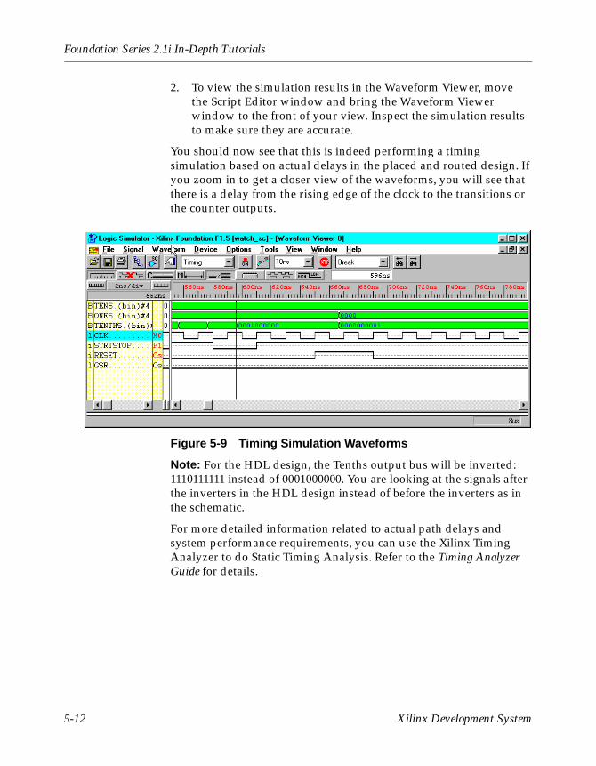
Foundation Series 2.1i In-Depth Tutorials
2. To view the simulation results in the Waveform Viewer, move the Script Editor window and bring the Waveform Viewer window to the front of your view. Inspect the simulation results to make sure they are accurate.
You should now see that this is indeed performing a timing simulation based on actual delays in the placed and routed design. If you zoom in to get a closer view of the waveforms, you will see that there is a delay from the rising edge of the clock to the transitions or the counter outputs.
Figure 5-9 Timing Simulation Waveforms
Note: For the HDL design, the Tenths output bus will be inverted: 1110111111 instead of 0001000000. You are looking at the signals after the inverters in the HDL design instead of before the inverters as in the schematic.
For more detailed information related to actual path delays and system performance requirements, you can use the Xilinx Timing Analyzer to do Static Timing Analysis. Refer to the Timing Analyzer Guide for details.
5-12 Xilinx Development System
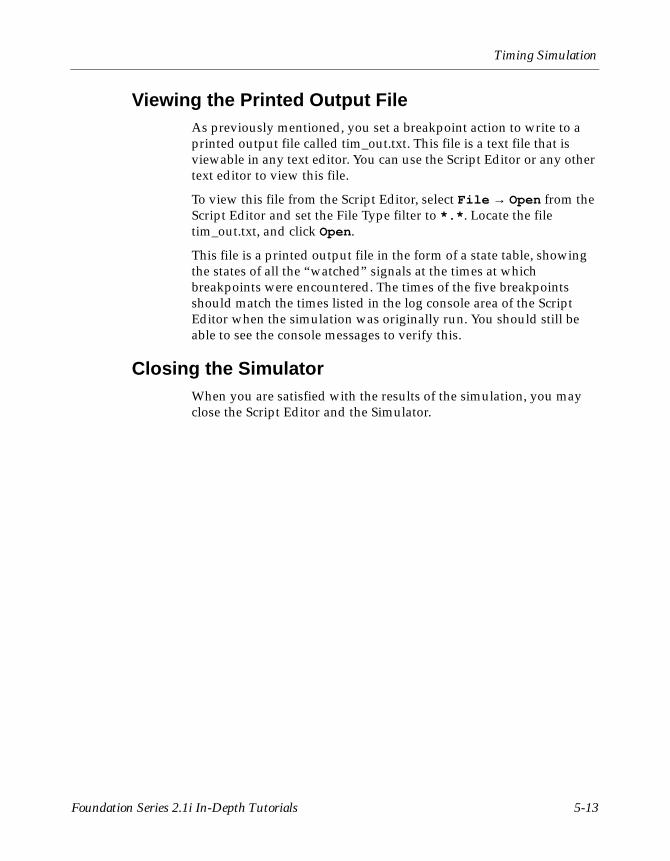
Timing Simulation
Viewing the Printed Output FileAs previously mentioned, you set a breakpoint action to write to a printed output file called tim_out.txt. This file is a text file that is viewable in any text editor. You can use the Script Editor or any other text editor to view this file.
To view this file from the Script Editor, select File → Open from the Script Editor and set the File Type filter to *.*. Locate the file tim_out.txt, and click Open.
This file is a printed output file in the form of a state table, showing the states of all the “watched” signals at the times at which breakpoints were encountered. The times of the five breakpoints should match the times listed in the log console area of the Script Editor when the simulation was originally run. You should still be able to see the console messages to verify this.
Closing the SimulatorWhen you are satisfied with the results of the simulation, you may close the Script Editor and the Simulator.
Foundation Series 2.1i In-Depth Tutorials 5-13

Foundation Series 2.1i In-Depth Tutorials
5-14 Xilinx Development System