fpga implementation and acceleration of building blocks
TRANSCRIPT

Portland State University Portland State University
PDXScholar PDXScholar
Dissertations and Theses Dissertations and Theses
1-1-2011
FPGA Implementation and Acceleration of Building FPGA Implementation and Acceleration of Building
blocks for Biologically Inspired Computational blocks for Biologically Inspired Computational
Models Models
Mandar Deshpande Portland State University
Follow this and additional works at: https://pdxscholar.library.pdx.edu/open_access_etds
Let us know how access to this document benefits you.
Recommended Citation Recommended Citation Deshpande, Mandar, "FPGA Implementation and Acceleration of Building blocks for Biologically Inspired Computational Models" (2011). Dissertations and Theses. Paper 160. https://doi.org/10.15760/etd.160
This Thesis is brought to you for free and open access. It has been accepted for inclusion in Dissertations and Theses by an authorized administrator of PDXScholar. Please contact us if we can make this document more accessible: [email protected].

FPGA Implementation & Acceleration of Building blocks for Biologically
Inspired Computational Models
by
Mandar Deshpande
A thesis submitted in partial fulfillment of therequirements for the degree of
Master of Sciencein
Electrical and Computer Engineering
Thesis Committee:Dan Hammerstrom, Chair
Douglas V. HallXiaoyu Song
Portland State Universityc©2011

Abstract
In recent years there has been significant research in the field of computational
neuroscience and many of these biologically inspired cognitive models are based on
the theory of operation of mammalian visual cortex. One such model of neocor-
tex developed by George & Hawkins, known as Hierarchical Temporal Memories
(HTM), is considered for the research discussed here. We propose a simple hier-
archical model that is derived from HTM. The aim of this work is to evaluate the
hardware cost and performance against software based simulations.
This work presents a detailed hardware implementation and analysis of the
derived hierarchical model. We show that these networks are inherently parallel
in their architecture, similar to the biological computing, and that parallelism can
be exploited by massively parallel architectures implemented using reconfigurable
devices such as the FPGA. Hardware implementation accelerates the learning pro-
cess which is useful in many real world problems. We have implemented a complex
network node that operates in real time using an FPGA. The current architecture
is modular and allows us to estimate the hardware resources and computational
units required to realize large scale networks in the future.
i

Acknowledgements
I am indebted to Dr. Dan Hammerstrom for his advice and suggestions throughout
the course of this work. There were numerous meetings and discussions that led to
successful completion of this thesis. I would like to thank all the members of our
reading group and give a special thanks to Mazad Zaveri who was always there to
help me when he was here and even after moving to India.
I am also grateful to the committee members, Dr. Douglas V. Hall and Dr.
Xiaoyu Song for reviewing this document and suggesting key changes.
I would like to thank Dr. Branimir Pejcinovic for providing me with an op-
portunity to be a part of the ECE department as a Teaching Assistant for various
courses.
My parents have always supported me in all my decisions and have always en-
couraged to take on new challenges for that I express my deepest gratitude and
love. I would like to thank all my friends Ketan, Abhijit, Priya, Ameya, Soniya,
Mihir, Omkar, Mrugesh, Makarand, Shantesh, Rajeev Nain, Ameya, Sudheer, An-
ish, Kapil, Jairaj for their support and enthusiasm.
ii

Contents
Abstract i
Acknowledgements ii
List of Tables vii
List of Figures viii
1 Introduction 1
1.1 Research Background and Motivation . . . . . . . . . . . . . . . . . 1
1.2 Objectives and My Contributions . . . . . . . . . . . . . . . . . . . 4
1.2.1 Objectives . . . . . . . . . . . . . . . . . . . . . . . . . . . . 4
1.2.2 Contributions . . . . . . . . . . . . . . . . . . . . . . . . . . 4
1.3 Thesis Structure . . . . . . . . . . . . . . . . . . . . . . . . . . . . . 6
2 Literature Review 10
2.1 Review: Biologically Inspired Hierarchical Cognitive Models . . . . 10
2.1.1 Mountcastle . . . . . . . . . . . . . . . . . . . . . . . . . . . 10
2.1.2 Hierarchical Temporal Memory (HTM) . . . . . . . . . . . . 11
2.2 Model Used In This Dissertation . . . . . . . . . . . . . . . . . . . 13
2.3 Vector Quantization (VQ) . . . . . . . . . . . . . . . . . . . . . . . 14
2.3.1 Vector Quantization . . . . . . . . . . . . . . . . . . . . . . 15
2.3.2 Choice of Codebook size . . . . . . . . . . . . . . . . . . . . 16
2.3.3 Initialization of Codebook . . . . . . . . . . . . . . . . . . . 17
iii

2.3.4 Distance Metric . . . . . . . . . . . . . . . . . . . . . . . . . 19
2.3.5 Learning Rate (α) and Epochs . . . . . . . . . . . . . . . . . 19
2.3.6 Competitive Learning Algorithm . . . . . . . . . . . . . . . 20
2.3.7 Frequency Sensitive Learning . . . . . . . . . . . . . . . . . 20
2.3.8 Resultant Codebook . . . . . . . . . . . . . . . . . . . . . . 20
2.3.9 Hierarchical Vector Quantization (HVQ) . . . . . . . . . . . 21
2.3.10 Analogy to an Artificial Neuron . . . . . . . . . . . . . . . . 22
2.4 Principal Component Analysis . . . . . . . . . . . . . . . . . . . . . 22
2.4.1 Get the data for PCA . . . . . . . . . . . . . . . . . . . . . 23
2.4.2 Calculation of Mean (DataMean) . . . . . . . . . . . . . . . 24
2.4.3 Covariance Matrix . . . . . . . . . . . . . . . . . . . . . . . 24
2.4.4 Obtain Eigenvectors . . . . . . . . . . . . . . . . . . . . . . 25
2.4.5 Projecting an input image with Eigenvectors . . . . . . . . . 28
2.4.6 PCA as a possible candidate for Intelligent System Node . . 29
3 BIHCM Used In This Dissertation 31
3.1 Combination of PCA & VQ to form a BM Module . . . . . . . . . . 31
3.1.1 Architecture . . . . . . . . . . . . . . . . . . . . . . . . . . . 31
3.1.2 Operation of part-A of the BM . . . . . . . . . . . . . . . . 33
3.1.3 Operation of part-B of the BM . . . . . . . . . . . . . . . . 36
4 Example: Handwritten Character Recognition System 39
4.1 Software Implementation of Recognition System . . . . . . . . . . . 39
4.1.1 USPS Dataset . . . . . . . . . . . . . . . . . . . . . . . . . . 40
4.1.2 System Parameters and Configuration . . . . . . . . . . . . 41
4.1.3 Training the System . . . . . . . . . . . . . . . . . . . . . . 43
iv

4.1.4 Testing the System . . . . . . . . . . . . . . . . . . . . . . . 44
4.1.5 Results . . . . . . . . . . . . . . . . . . . . . . . . . . . . . . 45
5 FPGA Design Flow & Development Tools 47
5.1 FPGA Design Flow . . . . . . . . . . . . . . . . . . . . . . . . . . . 47
5.2 FPGA Development Board . . . . . . . . . . . . . . . . . . . . . . . 50
6 BM Hardware Architecture 53
6.1 Hardware Design of part-A on FPGA . . . . . . . . . . . . . . . . . 53
6.1.1 On-line operation of part-A on FPGA . . . . . . . . . . . . 55
6.1.2 Xilinx - Block RAM . . . . . . . . . . . . . . . . . . . . . . 57
6.1.3 Ripple Carry Adder . . . . . . . . . . . . . . . . . . . . . . . 57
6.1.4 Multiplier Unit . . . . . . . . . . . . . . . . . . . . . . . . . 57
6.2 Hardware Design of part-B . . . . . . . . . . . . . . . . . . . . . . . 58
6.3 Precision Requirements of the Design . . . . . . . . . . . . . . . . . 63
6.3.1 Floating-point to Fixed-point Conversion . . . . . . . . . . . 63
6.3.2 Fixed-Point Precision Requirements for Part-A of a BM . . 66
6.3.3 Fixed-Point Precision Requirements for Part-B of a BM . . . 67
7 Results & Analysis 73
7.1 Design Verification Methodology . . . . . . . . . . . . . . . . . . . . 73
7.2 Performance Evaluation . . . . . . . . . . . . . . . . . . . . . . . . 76
7.2.1 Speedup . . . . . . . . . . . . . . . . . . . . . . . . . . . . . 76
7.2.2 Price (Area) . . . . . . . . . . . . . . . . . . . . . . . . . . . 80
7.2.3 Hardware Virtualization . . . . . . . . . . . . . . . . . . . . 82
7.3 Conclusion . . . . . . . . . . . . . . . . . . . . . . . . . . . . . . . . 84
v

7.4 Future Work . . . . . . . . . . . . . . . . . . . . . . . . . . . . . . . 86
References 88
vi

List of Tables
2.1 Codebook at Initialization . . . . . . . . . . . . . . . . . . . . . . . 18
2.2 Input Data for PCA Example . . . . . . . . . . . . . . . . . . . . . 23
4.1 Classification Accuracy Results . . . . . . . . . . . . . . . . . . . . 45
6.1 Precision Requirement of Input Variables . . . . . . . . . . . . . . . 67
6.2 Precision Requirement of Intermediate Variables . . . . . . . . . . . 68
6.3 Precision Requirement of Output Variables . . . . . . . . . . . . . . 69
6.4 Precision Requirement of Input Variables (part-B) . . . . . . . . . . 70
6.5 Precision Requirement of Intermediate Variables . . . . . . . . . . . 71
6.6 Precision Requirement of Output Variables . . . . . . . . . . . . . . 72
7.1 Verification Data for Data Adjust Block . . . . . . . . . . . . . . . 74
7.2 Verification Data for MAC Unit . . . . . . . . . . . . . . . . . . . . 74
7.3 Verification Data for Subtractor, Codebook Distances . . . . . . . 75
7.4 Verification Data for MinimumIndex Search Block . . . . . . . . . . 75
7.5 BM Single Module Parameters . . . . . . . . . . . . . . . . . . . . . 78
7.6 Response time Speedup . . . . . . . . . . . . . . . . . . . . . . . . . 80
7.7 Update Time Speedup . . . . . . . . . . . . . . . . . . . . . . . . . 80
7.8 Synthesis Results for two BMs . . . . . . . . . . . . . . . . . . . . . 80
vii

List of Figures
1.1 Typical FPGA Structure . . . . . . . . . . . . . . . . . . . . . . . . 6
2.1 Mini Column [15] . . . . . . . . . . . . . . . . . . . . . . . . . . . . 11
2.2 VQ Sample Image (Helicopter) . . . . . . . . . . . . . . . . . . . . 15
2.3 Processed Image with 287 ‘On’ pixels . . . . . . . . . . . . . . . . . 16
2.4 Plot of initial codevectors for VQ example . . . . . . . . . . . . . . 18
2.5 codevectors representing the input image . . . . . . . . . . . . . . . 21
2.6 (a)-VQ, (b)-Hierarchical VQ . . . . . . . . . . . . . . . . . . . . . . 22
2.7 PCA Data Sample . . . . . . . . . . . . . . . . . . . . . . . . . . . 23
2.8 Covariance Matrix for the example 2-D Dataset . . . . . . . . . . . 24
2.9 Plot of Principal Components showing Variance . . . . . . . . . . . 28
3.1 Main Components of BM Module . . . . . . . . . . . . . . . . . . . 31
3.2 Internal Mathematical Blocks of BM Module . . . . . . . . . . . . . 32
3.3 Hierarchical Arrangement of BM Modules . . . . . . . . . . . . . . 33
3.4 Flow of the Principal Component Extraction Process . . . . . . . . 34
3.5 Forward Mode of PCA . . . . . . . . . . . . . . . . . . . . . . . . . 34
3.6 Iterative Learning for Generating Codebook . . . . . . . . . . . . . 36
4.1 Input Image samples for Numeral-1 . . . . . . . . . . . . . . . . . . 40
4.2 Input Image Perceived by BMs in the Hierarchy . . . . . . . . . . . 41
4.3 Classification Accuracy Vs ‘N ′ . . . . . . . . . . . . . . . . . . . . . 46
5.1 Flow Diagram of major design steps . . . . . . . . . . . . . . . . . . 48
viii

5.2 FPGA Development Kit . . . . . . . . . . . . . . . . . . . . . . . . 52
6.1 Hardware Architecture for Online PCA . . . . . . . . . . . . . . . . 54
6.2 part-B: VQ Architecture . . . . . . . . . . . . . . . . . . . . . . . . 59
6.3 VQ in Vector Comparator Mode . . . . . . . . . . . . . . . . . . . . 60
6.4 VQ in Training/Learning Mode . . . . . . . . . . . . . . . . . . . . 61
6.5 Sequential Subtractor block . . . . . . . . . . . . . . . . . . . . . . 62
6.6 Floating to fixed point Conversion . . . . . . . . . . . . . . . . . . . 64
7.1 Waveforms for the DataAdj Block . . . . . . . . . . . . . . . . . . . 74
7.2 Waveforms for Row Feature Vector Matrix . . . . . . . . . . . . . . 75
7.3 Waveforms for MAC Unit . . . . . . . . . . . . . . . . . . . . . . . 75
7.4 Simulation Waveforms for Codebook Vectors . . . . . . . . . . . . . 75
7.5 Simulation Waveforms for Subtractor . . . . . . . . . . . . . . . . . 75
7.6 Pipelined Architecture . . . . . . . . . . . . . . . . . . . . . . . . . 77
7.7 Number of Neurons Simulated w.r.t the number of BM Modules . . 81
7.8 FPGA Resource Utilization w.r.t the number of Simulated Neurons 81
7.9 Virtualization of hardware resources: Update Logic . . . . . . . . . 83
7.10 Effect of Parallelization on Slack and Best Achievable Frequency . . 84
ix

Chapter 1
Introduction
1.1 Research Background and Motivation
This chapter will discuss some of latest trends in CMOS process technology, ad-
vances in Computer Architecture, and algorithms that are based on the concepts of
Biologically Inspired Hierarchical Cognitive Models (BIHCM). We also present an
overview of concepts and techniques that we have used in our hierarchical network
model. More detailed discussion is included in the respective chapters.
This thesis describes the Field Programmable Gate Array (FPGA) implemen-
tation of simple hierarchical model that is derived from George & Hawkins HTM
algorithm, and proposes an optimization technique to accelerate the learning pro-
cess. The model presented here is a generic one and can be used for building the
current models as well as future biologically inspired models. We have targeted the
primary bottlenecks of these models mainly growing vector length as we go up in
the hierarchy and finite memory requirements for a single module in the hierarchy
for carrying out vector comparisons. The comparison of a hardware implementa-
tion with a Software simulation was done and the results are promising for future
work in building large scale prototypes of these networks using FPGA devices.
The rate at which the semiconductor industry has grown over the last four
decades is phenomenal and is a result of advances in CMOS process technology.
Now the latest Intel processor chips are fabricated at 32 nm and are moving to 22
1

nm [14]. The deterministic nature of digital circuits soon is becoming more prob-
abilistic at increasingly smaller feature sizes. And their other problems discussed
by Hammerstrom [8]:
• Power Density: is one of the main challenges and limiting factors in perfor-
mance.
• Design complexity: more than 70% of the time is spent in verifying the
functionality
• Density overkill: how to best utilize a billion transistor chip?
• Limited deployment of parallel applications: the operating system and soft-
ware applications, which sit and run on top of the multi-core and multi-
threaded processors, needs to be developed to take full advantage of the
underlying hardware.
And although these problems are becoming more serious, Moore’s law contin-
ues. Instruction Level Parallelism (ILP), Multi-threading and Multi-Core architec-
tures are prominent examples. However due to the lack of parallelism in existing
software applications and Operating Systems which leads to under utilization of
the speed-up offered by underlying hardware and it proposes new challenges in the
way existing and future applications and operating systems will be developed.
Despite decades of research by the Artificial Intelligence (AI) community and
the enormous computing power available in today’s computers, we still struggle
with solving some of the very basic problems that animal nervous systems can
perform almost instantly which includes problems such as visual pattern and speech
recognition.
2

Biological systems are inherently parallel as opposed to traditional computers
which are primarily sequential architecture. This encourages the study of biology.
Its mathematical models needs to be explored in much more detail which will help
in the long term goal of building truly intelligent systems.
In recent years there has been a growing interaction between people from neu-
roscience and computer science which has led to the fantastic growth of this new
field of biologically inspired computing. The techniques presented in this work are
helpful when building custom chips for such intelligent computing models.
One of the active research groups who is looking at building a model of a
human neocortex based on the insights from neuroscience and computer science is
led by Jeff Hawkins at Numenta, Inc. They call their model Hierarchical Temporal
Memory (HTM) [5].
HTM consist of nodes that are arranged in a hierarchical manner. These nodes
essentially perform the same computation in all the layers in the hierarchy. This
makes their hardware implementation easier since only one node has to be designed,
which is then instantiated many times, based on the given hardware resources, the
application requirements, or to meet speed requirements of slower devices such as
memories. The degree of hardware virtualization [3] can be varied to effectively
use the available logic resources. Parallelism can be exploited at the node level.
Intra-node parallelism can be a major contributor in the overall speedup.
3

1.2 Objectives and My Contributions
1.2.1 Objectives
In this thesis we study several characteristics of HTM [5] that are essential for an
FPGA building block. Such a system should be adaptive in nature, have large
storage capacity per node, exploit the reconfigurable nature of FPGAs for on-line
learning and should scale to image size.
1.2.2 Contributions
This section highlights all the problems addressed by this work and our contri-
butions in solving those problems. The main goal of this thesis is to build a
simplified model based on the concepts of HTM and propose an optimization tech-
nique to accelerate the learning and recognition time of the model and also lower
the memory requirement of the proposed Bayesian Memory (BM) module which
is an approximation to the HTM node.
• Exploit the fine-grained parallelism that these models offer through hard-
ware implementation, propose a method for improving the performance of
the existing algorithm (which has only Vector Quantization (VQ) as its node
component) by introducing the use of Principal Component Analysis (PCA)
for dimensionality reduction/feature extraction and VQ for data compres-
sion.
• Determine the best integer approximation with fixed point precision.
4

• Compare and contrast Euclidean and Manhattan Distance metrics and com-
pare the PC-MATLAB simulation and FPGA implementation on various pa-
rameters to determine whether an FPGA implementation meets our expecta-
tions in the performance/price trade-off for building intelligent systems, and
analyze whether an FPGA offers performance advantage over PC-MATLAB
simulation.
• Although we discuss on-line training in our study, we assume that the feature
extraction is carried out in the offline phase and lookup and learning, which
are compute intensive, are carried out on-line with the recognition phase
being fully implemented in real time.
• We have focused on a single node and have multiple instances running in
parallel to increase the throughput of the system.
• We do not consider the inter layer communication or inter node communica-
tion.
FPGA ARCHITECTURE AND ITS ANALYSIS
Commercial computers and networked computers are best suited for simulation
and development purposes, but in order to build real time applications which
can benefit from these pattern recognition models we need to look at custom
hardware design space. FPGAs are well matched to such applications as they have
a reconfigurable structure and allow arbitrary parallelism. Figure 1.1 shows the
basic structure of a typical FPGA which has a matrix of configurable logic blocks
(CLBs) and interconnect between CLBs surrounded by I/O blocks. The FPGA
used in this work is in the intermediate range in terms of the number of gates and
5

other functionalities offered.
Figure 1.1: Typical FPGA Structure
In this work, our algorithm is implemented on a Xilinx Spartan 3E FPGA. It
shows significant speedup improvement over a PC implementation. The results
obtained proved the validity of our assumptions in using FPGAs for acceleration
and the real time implementation of such BIHCMs.
1.3 Thesis Structure
Chapter 2 covers the review of Biologically Inspired Computing and one of the lat-
est algorithms based on the same terminology. We then present the basic building
blocks of such systems and the proposed optimizations with appropriate examples.
Chapter 3 describes how the PCA is used in a HTM implementation and helps
in increasing the performance of the system.
Chapter 4 describes the design of a Bayesian Memory (BM) based Hierarchical
system and its application as a Handwritten character recognition system. We
perform classification over 10 different classes, we also discuss preprocessing tech-
niques and classification accuracy with and without our proposed optimization
6

technique.
Chapter 5 provides an overview of FPGA Design and Verification flow adopted
in the implementation of BM Module. Also it highlights some of the salient features
of the FPGA Device and board that is used for this work.
Chapter 6 describes the detailed hardware design and implementation of the
complete BM Module (part-A and part-B) along with Fixed-point precision dis-
cussion, internal blocks of the system and on-chip Block-RAM utilization.
Chapter 7 describes the verification techniques used here. It also presents a
performance analysis based on the speedup and area parameters. The concept
of hardware virtualization is discussed, which plays an important role in imple-
menting algorithms that are fine grained and can exploit parallelism based on the
performance/price trade-offs. Finally, the important findings are summarized in
the conclusions section and the future work section provides an overview of possible
additions and other considerations concerning future work.
7

Nomenclature
AI Artificial Intelligence
ANN Artificial Neural Network
BIHCM Biologically Inspired Hierarchical Computational Model
BM Bayesian Memory
BMI Bayesian Memory Implementation
CB Codebook
CV Codevector
DVM DataMean Vector Memory
FLP Floating Point
FPGA Field Programmable Gate Array
FV Final Vector is the output of part-A of the BM Module.
FXP Fixed Point
GPU Graphic Processing Unit
HTM Hierarchical Temporal Memory
InpVector Input Vector
LR Learning Rate ‘α′
8

LUT Look-up Table
MAC Multiply Accumulate Unit
MinIndex The winning index and the output of the BM Module.
PCA Principal Component Analysis
RVFM Row Feature Vector Memory
VQ/HVQ Vector Quantization/Hierarchical Vector Quantization
9

Chapter 2
Literature Review
This chapter covers the description of the ideas and concepts that are used in this
work in developing a model that enables efficient hardware implementation of the
compute intensive parts of an HTM. We first review existing Biologically Inspired
Hierarchical Cognitive Models and how they are related to the work presented.
Later we show how PCA, in addition to the VQ, is an effective solution for hardware
implementation of such models.
2.1 Review: Biologically Inspired Hierarchical Cognitive Models
2.1.1 Mountcastle
Mountcastle [16] in his book proposed that the basic unit of the neocortex is a
minicolumn and that the neocortex can be represented in columnar fashion. This
minicolumn is a vertically structured group of about 80-100 neurons. The combi-
nation of several of these minicolumns into a larger group is called a hypercolumn,
macrocolumn or simply a column, having dense connections within columns and
sparse connectivity between columns. This is shown in Figure 2.1.
10

Figure 2.1: Mini Column [15]
The dotted rectangle represents a macrocolumn/hypercolumn and small blue
containers within hypercolumn represents a minicolumn which is densely connected
where as hypercolumns are sparsely connected.
As can be seen from the Figure 2.1, most of the computations take place in
the column and a closer look reveals that the computations within a minicolumn
are uniform throughout a macrocolumn, which is the focus of this research work,
the hardware implementation of the most compute intensive part of the neocortex,
i.e., structure that resembles a minicolumn using reconfigurable hardware such as
FPGA. The details are discussed in the next chapter.
2.1.2 Hierarchical Temporal Memory (HTM)
Dileep George in his PhD thesis [6] proposed a theory on ‘how the brain might
work’ and introduced the notion of Hierarchical Temporal Memory (HTM). The
network is hierarchical in nature and has multiple HTM nodes in each layer of
the hierarchy. The HTM node has inputs and outputs and all the nodes perform
11

identical computations except for the top layer node, which has additional fea-
tures for performing classification. The HTM node is split into two operations
a spatial and a temporal pooler. The spatial pooler stores the unseen patterns
from the large set of input samples by making use of quantization. The winning
sequences from the spatial pooler are seen as groups by the temporal pooler and
these groups are formed using a greedy graphical grouping algorithm based on a
time adjacency matrix, which is generated from the first order transitions of spatial
pooler’s quantization centers.
As opposed to other learning methods, HTM along with spatial quantization
also exploits time as a teacher [10] for invariant pattern representation. This allows
the network to use the representations learned from one object in learning another
object. The network typically has a tree like structure and inputs are fed to the
bottom layer. The learning takes place by presenting to the network a continuous
stream of patterns in a movie like fashion.
Learning is done in a layer by layer manner. The bottom most layer receives
inputs from sensors and learns most likely temporal sequences by observing the
centers in the spatial pooler. Once all the nodes in the bottom layer finish learning,
they switch to recognition mode, in this mode all the nodes transmit the index of
the winning center in the spatial pooler that is closest to the current input sample.
Several of these bottom layer nodes are connected to a single node in the upper
layer of the hierarchy, which is the parent node and former is the child node. The
winning indices from several child nodes are concatenated and sent as an input
to the parent node. After child node learning is complete the parent node goes
into the learning mode and performs the same operation as child node. This type
of learning takes place throughout the hierarchy. The entire network functions
12

as a probabilistic inference network based on Pearl’s Bayesian Belief Propagation
algorithm (BBP).
2.2 Model Used In This Dissertation
We start with an analysis of existing models and incrementally built our model,
which becomes the base model for the hardware implementation and the baseline
for future FPGA implementations of BIHCMs.
• Today’s BIHCMs are based on the hierarchical organization of neocortex [11].
So we take that into consideration and organize our network as a hierarchy of
layers with each layer having multiple BMs. This approach has the advantage
of easier scaling than many traditional neural models.
• The most common characteristic of any BIHCMs is that they are memory
intensive, each BM module represents a dense internal interconnect structure
which means large memory requirements for a single BM module.
• Quantization, whether iterative or non-iterative, dictates the memory re-
quirements of an HTM node.
• Basic computational units in any model will have a vector quantizer for
mapping large number of input samples to a finite number of Codebook
vectors. The quantizer and its mathematical analysis is discussed in section
2.3.
• In our model we do not consider the temporal hierarchy in the HTM network.
13

• The proposed BM module covers the most fundamental computational blocks
and could be used to implement the temporal pooler if we were to build a
complete HTM.
• The same learning strategy is incorporated into our model, of layer by layer
learning. It turns out that this strategy is efficient and practical when hard-
ware implementation of such networks is considered.
• Coupled with layer by layer learning, with the computations being performed
by all the nodes in the layer as well as in the network, the concept of Hardware
Virtualization [3] can be effectively utilized for our implementation and is
discussed in chapter 7.
• The use of on-chip Block RAMs allows lower access times, thus increasing the
speed of operation which otherwise would be affected by the off chip accesses
to external dRAM.
• The entire network trains in an unsupervised, feed forward fashion [6]. For
our implementation, incidental feedback connections are not implemented.
2.3 Vector Quantization (VQ)
The basic vector quantization [7] can be defined as the process of mapping large
number of input samples to a smaller number of quantized centers which can be
used to reconstruct the original input with minimal sacrifice in the quality. It is a
fixed length to fixed length algorithm. VQ is widely used in the communication and
speech systems and it has become one of the best methods for data compression
of real signals. It is also used in image processing and video compression.
14

Some of the advantages of VQ are (a) simplicity, (b) adaptive nature and (c)
potential parallelism and speed. The algorithm used in this work is explained with
the following example.
2.3.1 Vector Quantization
An example image is shown in Figure 2.2. Preprocessing involved conversion to a
grayscale image with 2-dimensional data points representing the image. Here we
have resized the image to a 50× 50 square.
Figure 2.2: VQ Sample Image (Helicopter)
A preprocessed Image, that is represented by pixels is shown in Figure 2.3.
15

0.2
0.25
0.3
0.35
0.4
0.45
0.5
0.55
0.6
0.650.25 0.3 0.35 0.4 0.45 0.5 0.55 0.6 0.65 0.7
Figure 2.3: Processed Image with 287 ‘On’ pixels
T = [x0, x2, ..., xM−1] (2.1)
The source vectors are k- dimensional, e.g.
xm = (xm,1, xm,2, xm,3, xm,4, ...., xm,k), m = 1, 2, 3, ...M (2.2)
2.3.2 Choice of Codebook size
Once the training dataset is obtained, the next step is to select the number of code-
vectors CV in the the Codebook. Let N be the total number of codevectors and C
represent the Codebook in Eqn 2.3. Then each codevector will be k-dimensional
16

as shown in Eqn 2.4 below:
C = (c1, c2, c3, ..., cN) (2.3)
Each Codevector will be
cn = (cn,1, cn,2, cn,3, cn,4, ..., cn,k), n = 1, 2, 3, ....., N (2.4)
In our example, the Codebook size can be selected to be a value less than
the total number of training samples. In our example we select N = 15. Now
the codebook will have 15 codevectors and k = 2, which defines the size of the
Codebook.
2.3.3 Initialization of Codebook
Having selected the number and dimension of the codevectors, now the initial
values can be assigned to these codevectors. There are several ways [7] to do this
but we will initialize the Codebook with random points in the input space. The
resulting Codebook is as shown in Table 2.1 for a 2-dimensional example.
17

Index of codevector X Y1 0.763 0.31172 0.7191 0.23753 0.9897 0.42354 0.0573 0.85075 0.3384 0.22046 0.3679 0.42647 0.5262 0.8168 0.3667 0.26519 0.6008 0.947810 0.908 0.774111 0.5626 0.005512 0.6662 0.064513 0.5128 0.26614 0.2118 0.066215 0.9491 0.1497
Table 2.1: Codebook at Initialization
0 0.2 0.4 0.6 0.8 10
0.1
0.2
0.3
0.4
0.5
0.6
0.7
0.8
0.9
1
Figure 2.4: Plot of initial codevectors for VQ example18

2.3.4 Distance Metric
For each new source vector xi, the winner CV is selected from the Codebook. The
winning CV is the closest to the given source vector and this is calculated either
by a Least Square Error or by a Manhattan Distance Metric or any other measures
as described in [7]. Here we will consider only these two distance measures.
The least square measure or Euclidean Distance Measure is defined by the
following equation:
di = Σi=N,k=Di=1,k=1 ((codevectori,k − xi,k)2)1/2 (2.5)
The Manhattan Distance Metric is defined as:
di = Σi=N,k=Di=1,k=1 (abs(codevectori,k − xi,k)) (2.6)
2.3.5 Learning Rate (α) and Epochs
Learning Rate (α): This parameter decides the rate at which the winning code-
vector CV will be adjusted in order to move it closer to the source vector on each
iteration. The general range for α is set between 0.1 to 0.0001. If the value is too
high, the CB may not best represent the input space so the value is in the lower
range.
Epoch: This parameter indicates the number of iterations for which the entire
training set of source vectors will be scanned in order to obtain the desired Code-
book which represents the input space. Epoch is defined at network initialization.
To avoid under or over training of the CB, Epoch was varied from 1 to 100 in order
to find the best Codebook that will represent the input space with minimum loss
19

of information while reconstructing the original image with quantized codevectors.
2.3.6 Competitive Learning Algorithm
Adaptive Algorithm: Equation 2.7 shows how the codevectors are trained on the
source vectors ‘X ′i to eventually represent the entire input space with codevectors.
Usually the number of codevectors is quite a bit less than the total number of
InpVectors.
CVi = CVi + α× (Xi − CVi) (2.7)
‘i′ in above equation represents the codevector that is closest to the given source
vector Xi.
2.3.7 Frequency Sensitive Learning
In case of competitive learning, some codevectors may be lost during learning and
are never utilized for data compression. By penalizing the frequently winning
codevectors, we can guarantee that all the codevectors are used to represent input
space.
2.3.8 Resultant Codebook
After the specified number of Epochs, the Codebook is said to have adapted to
represent the entire input space. The red points in the Figure 2.5 represent the
Codebook (CB) and the gray points are the original points from input image.
20

Figure 2.5: codevectors representing the input image
2.3.9 Hierarchical Vector Quantization (HVQ)
In order to simplify the design, it may be possible to use hierarchical vector Quan-
tizer [12] as shown in Figure 2.6. The advantage of using a hierarchy is that the
input dimension of the Quantizer node in (b) is two, where as for Quantizer node
in (a) it is four. The Quantizer in Figure 2.6 (b) requires a smaller codebook and
hence requires less memory for its hardware implementation.
21

Figure 2.6: (a)-VQ, (b)-Hierarchical VQ
2.3.10 Analogy to an Artificial Neuron
Each codevector is very roughly equivalent to a single artificial neuron based in
most ANN models. So the total number of neurons is equal to the number of
codevectors in a Codebook. In the analysis section, we will see how to estimate
the total count of simulated neurons based on the multiple BM modules running
in parallel.
2.4 Principal Component Analysis
In a system where there may be a large number of potential patterns, it is nec-
essary to represent the new input pattern using a set of predefined occurrences.
22

This can be done by using Principle Component Analysis (PCA) [12]. In the hi-
erarchical model which we present, PCA plays an important role in simplifying
the computation of exhaustive search through large Codebooks at the expense of
additional memory for storing the Eigenvector matrix and DataMean vector.
2.4.1 Get the data for PCA
Here a simple example of PCA is presented. The idea is to introduce PCA and
how it simplifies building a hierarchical model. The dataset is random and 2-
dimensional and is generated by MATLAB.
0 1 2 3 4 5 60
1
2
3
4
5
6
Data Points
Figure 2.7: PCA Data Sample
X 1 1.2 1.4 0.8 2 2 2.8 3 3.2 2.5 4 4.5 4.4 5 5.1 5.3 5.5 6
Y 2 1.8 2.4 2.9 1.5 2.3 3 1.9 2.5 2.8 3.1 3.6 2.8 3 4.2 4.8 3.9 4.4
Table 2.2: Input Data for PCA Example
23

2.4.2 Calculation of Mean (DataMean)
In order to compute the covariance, first the average of each dimension needs to
be calculated. Equation 2.8 is used to calculate the average of the data in each
dimension. We define mean vector as DataMean Vector in coming chapters.
X =Σd
i=1Xi
d, Y =
Σdi=1Yid
(2.8)
2.4.3 Covariance Matrix
The covariance is a measure of how much the dimensions vary from the mean with
respect to each other. For an M dimensional dataset, the covariance matrix will
have M ×M elements, and can be computed using Equation 2.9.
cov(X, Y ) =Σd
i=1(Xi −X)(Yi − Y )
(d− 1)(2.9)
In Equation 2.9 X and Y are the mean values of the respective dimensions. Using
Equation 2.9 to generate the covariance matrix for our sample dataset, we get the
following:
cov(x, x) cov(x, y)
cov(y, x) cov(y, y)
=
2.901417 1.277549
1.277549 0.873105
Figure 2.8: Covariance Matrix for the example 2-D Dataset
This matrix provides information about the nature of the data. cov(x,y) and
cov(y,x) are the same, indicating that the dataset has a positive correlation. If
24

either covariance value is negative, it indicates that as X increases Y decreases. If
the covariance value is zero it means that X and Y have no correlation.
It is easy to visualize or plot 2D and 3D data but more difficult to visualize
high dimensional dataset which is where covariance is most widely used to find the
relationships between dimensions in high-dimensional datasets.
2.4.4 Obtain Eigenvectors
Given a square matrix A and λ which is the Eigenvalue for a given non-zero
vector X, constrained by Equation 2.11. ‘X’ is the Eigenvector associated with the
Eigenvalue λ for matrix A can be found out by Equation 2.10
det(A− λ · I) = 0 (2.10)
(In Equation 2.10 ‘det′ stands for determinant and ‘I ′ stands for Identity Matrix)
A ·X = λ ·X (2.11)
Calculating Eigenvalues for A. A is a covariance matrix from our example.
2.901471 1.277549
1.277549 0.873105
− λ 0
0 λ
=
2.901417− λ 1.277549
1.277549 0.873105− λ
Solving the above matrix subtraction,
25

det
2.901417− λ 1.277549
1.277549 0.873105− λ
= (2.901417− λ)(0.873105− λ)− (1.277549)(1.277549)
= (2.901417− λ)(0.873105− λ)− 1.63213
= λ2 − 3.77452λ+ 0.901111
λ1 = 0.256123
λ2 = 3.518452
These are 2 Eigenvalues for the covariance matrix ‘A′. With covariance matrix
and its Eigenvalues now we can compute the Eigenvectors.
For a Given matrix: A =
a b
c d
If the c is not zero then Eigenvectors can be defined as:
Eigenvector1 =
∣∣∣∣∣∣∣∣λ1 − d
c
∣∣∣∣∣∣∣∣ , Eigenvector2 =
∣∣∣∣∣∣∣∣λ2 − d
c
∣∣∣∣∣∣∣∣ (2.12)
and if b is not zero then:
Eigenvector1 =
∣∣∣∣∣∣∣∣b
λ1 − a
∣∣∣∣∣∣∣∣ , Eigenvector2 =
∣∣∣∣∣∣∣∣b
λ2 − a
∣∣∣∣∣∣∣∣ (2.13)
Substituting values of λ1 and λ2 in 2.12 , We get:
26

Eigenvector1 =
∣∣∣∣∣∣∣∣0.434883
−0.90049
∣∣∣∣∣∣∣∣ , Eigenvector2 =
∣∣∣∣∣∣∣∣−0.90049
−0.43488
∣∣∣∣∣∣∣∣After calculating the Eigenvectors and Eigenvalues of the Covariance Matrix, vari-
ance in the original dataset is now available. The star marked points in Figure 2.9
are normalized, i.e., where the mean is subtracted from each point. As can be seen
in the same Figure 2.9, two principal components are orthogonal to each other.
The first principal component points in the direction of the maximum variance in
the data and second principal component is orthogonal to the first component, as
it shows the variance with respect to the first one. Eigenvectors are arranged in an
ascending order based on their corresponding Eigenvalues. Two lines on the plot
in Figure 2.9 are obtained from Eigenvectors.
27

−4 −3 −2 −1 0 1 2 3 4−4
−3
−2
−1
0
1
2
3
4
Normalized Data
2nd Principal Component
1st Principal Component
Figure 2.9: Plot of Principal Components showing Variance
2.4.5 Projecting an input image with Eigenvectors
The steps discussed in explaining PCA, helps us understand how it works and
where it can be applied. The use of PCA for dimensionality reduction in image
processing applications is wide spread. For a given dataset with sample images,
the image can be represented by a single row of concatenated pixels or a single
column for each image. The covariance matrix, Eigenvalues and Eigenvectors for
this dataset are found out by following the steps discussed earlier.
In our example, these Eigenvectors and the newly formed Eigen space is for the
numerals 0-9 and can be called as Eigen digits space. All the Principal Components
28

together represent the entire input space. As seen earlier, typically only the first
few principal components represent most of the variance in the given dataset.
Only using the N components with high variance, the dimensionality of the input
dataset is reduced to only N -dimensions.
New input image can be represented by any one of the Eigen digits with only
N dimensions. Also Eigenvectors can be used to project the input image by sub-
tracting the DataMean from the input image and multiplying the outcome with
Eigenvector matrix.
2.4.6 PCA as a possible candidate for Intelligent System Node
For example if the input image is 16 × 16, we can partition it into 16 regions of
4 × 4 each. Each node in Layer-1 takes as input one of the regions of the entire
image. Lets consider the (1,1) node which has the receptive field of only the upper
left block of the total image. Its input is a [4× 4] = 16 element wide vector. Four
Layer-1 nodes are seen by each Layer-2 node. So the concatenation of the output
of four such nodes forms the input vector to the Layer-2 node.
The concatenated vector length grows as the input image has higher resolutions
and it becomes difficult to pass these long concatenated vectors up the hierarchy.
By introducing PCA as one of the components in the node, now the vector length
seen by a VQ in any layer in the hierarchy can be made uniform by selecting only
the first N principal components. This directly reduces the computation time
required to compare the input vector with all the codevectors in the CB. As the
codevector length reduces, the total memory required for the Codebook is less as
compared to the design without the PCA.
An image is represented by a set of pixels. These pixels can be arranged in a
29

row or column forming a vector. Similarly all the images can be arranged in the
same fashion. This forms our image vector matrix. Principal component analysis
which resides in the node receives this image matrix and computes Eigenvalues and
Eigenvectors in order to compute the first N principle components. This process
need only be done once, The Eigenvectors are stored in the node memory along
with the DataMean vector for that dataset.
30

Chapter 3
BIHCM Used In This Dissertation
3.1 Combination of PCA & VQ to form a BM Module
In this section, we propose a novel node architecture, and provide all the necessary
details on its internal and external operation and subsequent role in the hierarchy.
For this implementation we do not consider Temporal Pooling and concentrate
only on optimizing Spatial pooling.
3.1.1 Architecture
The architecture of a proposed node is shown in Figure 3.1 We use the term BM to
refer to Bayesian Memory (BM). Because under certain conditions the VQ exhibits
Bayesian properties [17]; in general, BM is an approximation to the HTM node
and refers to a single module and not the entire hierarchical structure.
Figure 3.1: Main Components of BM Module
31

Figure 3.2: Internal Mathematical Blocks of BM Module
A single BM module consists of two functional parts: part-A and part-B [9].
During the learning phase, part-A extracts Eigenvectors and DataMean from input
dataset and part-B builds a Codebook (CB) based on these projected InpV ectors
with reduced dimensions. The Row Feature Vector Matrix (RFVM), DataMean
Vector (DVM) and CB are in a physical Memory for the proposed BM Module.
Here the necessary mathematical components and one possible optimization
technique for implementing Hierarchical Network Models and provide working and
synthesizable component modules for future implementations of such algorithms.
For the current FPGA implementation we have implemented parallelism at the
Module level. All the internal operations are performed sequentially.
Multiple BM modules can be connected in a tree structure to form a hierar-
chical system as shown in Figure 3.3 (this also has called Hierarchical Distributed
Memories in some of the earlier work by our research group [9]. This is illustrated
in Fig 3.3 and the details of the operation of BM based hierarchical system as
32

shown in Figure 3.3 are provided in the following sections. In Figure 3.3 each layer
has several BM modules, for example, Layer-1 has 16 BM modules, Layer-2 has 4
BM modules and Layer-3 has only single BM module. Since these BM modules are
arranged in a hierarchical manner the network is called a BM based hierarchical
network.
Figure 3.3: Hierarchical Arrangement of BM Modules
3.1.2 Operation of part-A of the BM
The primary function of part-A of the BM is to find the first N Principal Compo-
nents which requires the Eigenvectors and DataMean vector for all the incoming
vectors of the particular BM module. Through this process, RVFM and DVM are
built and stored in the respective BM modules. The process of feature extraction
or dimensionality reduction is achieved by a single pass through the entire training
dataset.
33

3.1.2.1 Finding Principal Components for the Layer-1 BM
Figure 3.4 shows the step by step process [2] for the formation of RVFM and DVM
for a single BM module. The training dataset is directly passed onto all the Layer-
1 BM modules. Preprocessing involves the subdivision of input image into non-
overlapping regions depending on the size of the image and network configuration.
DVM
Correlation Matrix
Eigen Analysis
Sort Principal Components
Mean Vector Compute Block
Training Dataset
RVFVM
Figure 3.4: Flow of the Principal Component Extraction Process
FViData Adjust Block
Map to Eigen Space
Feature Vector GenerateInpVector
Data Mean [DVM]
EigenVec [RVFM]
Figure 3.5: Forward Mode of PCA
Once the Layer-1 BM extracts Eigenvectors and DataMean vector for the train-
ing dataset, it then goes in forward mode of operation as shown in Figure 3.5.
A BM in forward mode does the following: The mean vector from the training
dataset which is called the DataMean vector is first subtracted from the incoming
InpV ector. The resulting vector, which is called the DataAdjust Vector, has the
34

same dimensions as the InpV ector. The RVFM that was generated during the
learning phase is an N ×M matrix, in which N is the number of principal com-
ponents that we decided to keep and M is the length/dimension of the original
InpV ector. Next, each of the RVFM vectors is multiplied by DataAdjustVector
to generate the FinalVector (FV ) which is a projection of InpV ector onto an N
dimensional Eigen digits space.
3.1.2.2 Finding the Principal Components for Layer 2 and above
In Figure 3.3, consider a Layer-2 BM, we want to find N principal components
and form the respective Eigenvector memory/RVFM and DataMean Vector mem-
ory/DVM for each Layer-2 BMs. Each Layer-2 BM has several Layer-1 BMs
connected to it. Layer-1 BMs receives their inputs directly from the training
dataset. Layer-2 BMs receive the concatenated vectors of all the Layer-1 BM
winning vectors (WinV ) they are connected to. So the input to each Layer-2
BM is InpV ector = (WinV1,1WinV1,2WinV1,3WinV1,4). Note that the InpV ector
for a Layer-2 BM is not the direct input from sensors, but the quantized ver-
sion/approximation of input image. The calculation and message passing of win-
ning vectors (WinV ) is covered under section 3.1.3. Once the Layer-2 BM has
finished their learning, they all will go in the forward mode of operation and gen-
erate WinV for each subsequent Layer in the hierarchy which in our example is
Layer-3. At any given point during the learning phase, a given BM has to only
communicate with BMs that are one Layer above itself. So, for example, during
the learning of Layer-3 BM it has to communicate with only Layer-2 BM modules
and not Layer-1 BM modules.
35

3.1.3 Operation of part-B of the BM
In part-A of each BM module, we looked at the steps involved in generation of
RVFM and DVM. Also we saw that during the training phase of BM, part-A
generates FV which is a projection of original InpV ector onto an Eigen digits
space using Eigenvectors. FV acts as a training vector for the VQ block.
3.1.3.1 Learning the CB for each Layer-1 BM module
Start
End
Randomly Initialize
Codebook
Find min distance
And its index
Compute Distances
Update the
Centerindex
i
>Epochs
Yes
No
Figure 3.6: Iterative Learning for Generating Codebook
The CB is a matrix of size R × C where R is the number of rows representing
unique codevectors having a vector length of C. All the codevectors are randomly
initialized. Using Euclidean/Manhattan Distance Metric, the distance d between
each CB codevector and FV is determined. After finding the minimum of all
36

the distances in the distance table, the codevector with this smallest distance is
chosen as the winner. An update rule (adaptive algorithm) in 2.3.6 is applied to
the winner with fixed α. The epoch size determines the number of iterations &
hence the convergence time. In Figure 3.6 we show the iterative learning for CB
generation.
Once the CB finishes its learning (i.e. when all training vectors have been
presented for defined number of epochs), part B goes into the forward mode of
operation as shown in Figure 3.6. In the forward mode the distance between each
CBi codevector and the FV are determined and stored in the distance table along
with their unique indices. After finding the minimum of all the distances in the
distance table, the codevector with the smallest distance value is chosen as the win-
ning vector (WinV ) and its associated index represents BM upward outputs. The
purpose of sending the index of the WinV is evident when hardware implementa-
tion is considered. On FPGA it is not possible to pass the concatenation of WinV
to BM in the upper layers, therefore by storing their indices, much less bandwidth
is used. Indices can be directly used as a pointer to the memory locations where
the WinV are stored.
3.1.3.2 Learning the CB for Layer-2 BM module
Earlier it was shown how InpV ector is formed and the N principal components
are computed. Once RVFM and DVM are generated for the dataset formed by
InpV ectors; we can proceed with the learning of CB for each Layer-2 BM module.
We will denote FVi=2 as the Feature Vector at Layer-2 which becomes an input
vector for generating Layer-2 CBs. The learning is same as that for Layer-1 BM.
Only the difference being, the size of the CB at Layer-2 could be larger or smaller
37

compared than the rest of the CBs in the hierarchy.
3.1.3.3 Learning the CB for Layer-3 BM module
The learning strategy for the Layer-3 CB is little different in the sense that this
BM module has to perform the function of classification as well. In our example,
we have 10 different classes and each class represents a unique numeral 0-9. The
codevectors in the CB at this Layer are split into 10 classes with groups of several
codevectors representing each class. After getting FV3 from part A of Layer-3
BM, FV dataset is sorted based on the class to which each FV belongs and these
individual datasets are used as training data for learning the CB at Layer-3. For
analysis of this work, we have considered a 3 level hierarchy. The number of layers
in the hierarchy are arbitrary and in this work Layer-3 is the last level that is
relevant.
38

Chapter 4
Example: Handwritten Character Recognition System
4.1 Software Implementation of Recognition System
In this section we show a MATLAB simulation of a hierarchical system which con-
sists of BMs. The system is configured to do a handwritten character recognition.
If we remove Temporal pooling from the HTM node, the underlying algorithm and
network structure is basically a Hierarchical Vector Quantizer (HVQ) [7]. The very
first recognition system we built had VQ only as a node component and the net-
work is Hierarchical Vector Quantizer Network without the PCA as optimization
technique. The type of learning is unsupervised and hence we ignore top down
(feedback) communication in the hierarchical system.
Increasing vector length coupled with less number of iterations result in high
conversion time and poor classification accuracy. Also, Manhattan Distance met-
ric requires large Epochs to improve the classification accuracy .As discussed in
section 3.1.2.2, BM nodes in layers other than Layer-1 receive InpVector which is
a concatenated version of all the winner vectors from the immediate lower layer
BMs connected to it. The growing vector length puts serious limits on the memory
requirements of CBs of BMs.
The introduction of PCA along with HVQ allowed faster convergence time and
reduced the time for an extensive search for the minimum distance codevector in
a large CB. This type of BM requires fewer CB codevectors and WinV search
is faster. Also PCA extracts eigenvectors which allow us to project an unknown
39

input image to the closest possible match from a given set of Eigenvectors.
4.1.1 USPS Dataset
The USPS handwritten numerals dataset is used to test our system. The dataset
is readily available in a MATLABb compatible format. It can be downloaded
from the web from [18]. It is a very common dataset used extensively in pattern
recognition and machine learning research. The USPS dataset consists of 7000
train images and 4000 test images. All the images are grayscale with a resolution
of 16× 16 pixels and can be converted to their binary version by preprocessing.
Figure 4.1: Input Image samples for Numeral-1
Preprocessing Technique Figure 4.1 above is an image directly obtained
from sensors and needs preprocessing before it is input to the recognition system.
An overview of BM arrangement in the hierarchical recognition system and how
an input image is perceived by BMs in different layers is illustrated in Figure 4.2.
40

Figure 4.2: Input Image Perceived by BMs in the Hierarchy
Layer-1 BMs have a limited receptive field and only each see 1/16th of the entire
input image. Similarly, each Layer-2 BM see 1/4th of the entire image and only
Layer-3 can see the entire image.
4.1.2 System Parameters and Configuration
Overall system configuration for HVQ and PCA-VQ is the same in terms of the
number of layers and the number of BM modules at each layer. The preprocessing
performed on an input image remains the same for all the variations of the system.
4.1.2.1 Parameters specific to the HVQ System
A vector quantizer, when arranged in a hierarchical structure has three parameters
that govern the training and testing of the system.
41

• Number of codevectors in a CB
The VQ uses fixed number of iterations to train the CB and the number of
codevectors, i.e., the size of the CB is variable and needs to be determined via
trial and error. It is also dependent on the number of training Epochs. If the
number of Epochs is small, the CB size required will be very large in order
to store all the variations in the input dataset, and if the epoch size is large,
the training time is large and also it impacts the hardware implementation
because it increases the demand on the Fixed-point precision (FXP) as values
in the trained CB have higher precision requirements.
• Learning Rate ( α )
Codevectors are updated on an incremental basis and this increment in the
winning codevector is controlled by α. If the codevectors are initialized in
the same range as that of input vector range then α could be very small,
otherwise between 0.1 to 0.0001 is the usual range for this variable.
• Epoch size
Number of iterations for which the individual input vector is seen by the BMs
is variable and completely depends on the size of training dataset, initial
values of the CB and α. Epoch size can be defined for individual BMs in a
layer or could be same for all the BMs in any given layer.
4.1.2.2 Additional Parameters for PCA-VQ BM System
In addition to the parameters discussed in section 4.1.3.1, we have an additional
parameter ‘N ′, which is the number of principal components that will be extracted
from the input dataset. Note that N cannot exceed the maximum value of the
42

input dimension. For example if the input vector is 16 elements wide, the maximum
number of principal components that can be extracted is N = 16.
The value of N can be different for different layers in the hierarchical network.
For example, at Layer-1 we may extract first 4 principal components out of 16
dimensional input vector and discard the remaining 12 components similarly at
Layer-2 we may again extract only first 4 components and so on.
In PCA-VQ BM system, in addition to CB memory, we have Eigenvectors
(RFVM) and DataMean Vector (DVM) memory blocks. These memories are built
/ generated during the training phase and are active throughout the operation of
the network.
4.1.3 Training the System
After preprocessing, each image in both the train and test datasets is subdivided
into logical blocks representing 16 non-overlapping regions. We use this newly
formed dataset for our system. Each Layer-1 BM receives its InpVector corre-
sponding to one of the 16 blocks of the original image. To capture the entire
image, we need 16 Layer-1 BM modules. By concatenating the outputs (WinV) of
four adjacent Layer-1 BMs, an input vector to one Layer-2 BM is formed. Similarly
all the Layer-2 BM outputs are combined to form an input vector to the Layer-3
BMs. It can be observed that all the inputs going to Layer-1 form a hidden layer
and can be labeled as Layer-0 in the hierarchy.
Initialization includes filling up all the CBs in all the BMs with random values.
The user needs to define the α, Epochs and total number of principal components
N to be extracted at each layer in the hierarchy. Note that each layer may have a
different N value.
43

In the case of the HVQ system, the input vector to Layer-2 and above is a direct
concatenation of four of the lower level adjacent BMs. The Layer-3 learning also
takes place in the same manner. Each numeral class has a bell shaped probability
distribution that is called a Gaussian Window and the classification at Layer-3 is
achieved by comparing the output of Layer-3 with each of the class distribution
values. In total we will have 10 Gaussian windows representing 0-9 numeral classes.
For the PCA-VQ BM System, all the Layer-1 CBs, RVFMs and DVMs are
trained and generated using the procedures discussed in Chapter 3. In order to
reconstruct the FV during the testing phase, RFVM and DVM are stored in each
BM. Only one layer is trained at a time. This concludes the training of our system.
4.1.4 Testing the System
A trained network consists of BMs with trained CBs, RVFMs and DVMs repre-
senting one particular block out of either 16, 4, 1 blocks of input image depending
on where the BM is situated in the hierarchy.
During the testing of the network, all the BMs in the network operate in the
forward mode of operation. For a given input test image the corresponding FV is
generated by part-A of a BM and the closest match out of the CB codevectors is
declared a winning vector (WinV) and is the output of the module. This process
continues up the hierarchy until Layer-3. The classification task is performed at
Layer-3; this is achieved by first arranging the distance values in the distance table
in an ascending order, the associated indices represent the location of WinV out
of all the CB codevectors. To find an input’s class, the index value is divided by
the total number of codevectors that are assigned to each class. For example, if
Layer-3 has 50 codevectors in its CB, the index associated with WinV is divided
44

by 5 (there are total 10 classes i.e. 5 codevectors per class). The resulting value is
rounded off to the nearest integer value that is greater than or equal to the index
value.
4.1.5 Results
Parameters Network Configurations
N1 N2 N3 N4 N5 N6 N7
Layers (1,2,3) 1, 2, 3 1, 2, 3 1, 2, 3 1, 2, 3 1, 2, 3 1, 2, 3 1, 2, 3
CB Size (×10) (3,5,10) (3,5,10) (7,5,10) (7,5,10) (10,3,10) (20,50,10) (3,3,10)
No. of Principal
Components N
4,8,16 4,4,4 6,6,6 10,12,12 10,10,10 16,32,32 16,32,32
Epochs (×10) (1,1,10) (1,1,10) (1,1,20) (1,1,20) (10,10,20) (10,10,10) (1,1,10)
Learning Rate 0.01 0.01 0.01 0.01 0.01 0.01 0.01
Multiplier (for
random init of
codevectors)
10*rand 10*rand 10*rand 10*rand 10*rand 10*rand 10*rand
Accuracy
Trainset-1st
best match
90.61 71.14 82.4 89.03 88.39 94.33 89.76
Trainset-1st &
2nd best match
95.29 85.26 91.07 94.67 93.91 97.34 94.93
Test set-1st best
match
89.12 68.9 81.05 88.92 87.92 92.75 88.5
Test set- 1st &
2nd best match
94.1 83.3 89.55 94.7 93.35 96.25 93.93
Table 4.1: Classification Accuracy Results
The plot in Fig 4.3 shows the classification accuracy for the BM based hierarchical
character recognition system. The accuracy is shown as the best predicted and the
45

second best match for the given input.
4681012141670
75
80
85
90
95
100
Number of Principal Components ’N’
Cla
sific
atio
n A
ccur
acy
in %
1st Best Match
1st + 2nd Best Match
Figure 4.3: Classification Accuracy Vs ‘N ′
It can be observed from the Table 4.1 that, just increasing the Codebook size
does not guarantee 100% accuracy. Therefore by the process of feature extraction
we can reduce the Codebook sizes without the loss in the recognition accuracy.
Also, the hardware cost of on chip memory for the Codebook is reduced signifi-
cantly. For example, in a given image, if the input vector is 16 dimensional and we
extract principal components and only first 4 are stored then the required memory
is 1/4 the original size.
46

Chapter 5
FPGA Design Flow & Development Tools
The major component of any design process is the description of the design in
a suitable form using a hardware description language to program in the FPGA.
For verification of the developed RTL, we need to have a reference model with
which the hardware results can be compared. The initial design was developed
using Floating-point precision in MATLAB. Once the algorithm functionality was
verified, then for the FPGA implementation the Fixed-point model of the algorithm
was developed in the MATLAB for verification. For debugging of the synthesized
design on the FPGA, an interactive user interface and available indicators on the
FPGA board were used throughout the design cycle.
The development process consists of two major steps: the MATLAB Design
Space for Debug & Verification and FPGA Design Flow for Synthesis, Place &
Route and to download the design into an FPGA. The combination of these two
forms a complete development flow as shown in Figure 5.1.
5.1 FPGA Design Flow
This section covers all the necessary steps required to realize the design concept in
an FPGA, and provides details of the particular FPGA device used in this work.
The entire design was developed using the Verilog-HDL [13], synthesizable con-
structs must be used. Synthesis is the process of converting an HDL design into a
device netlist format for the FPGA implementation.
For large, complex designs, the synthesis process can be time consuming.
47

Figure 5.1: Flow Diagram of major design steps
Therefore as the design complexity increases it is necessary to verify the func-
tionality of the design before proceeding with synthesis. ModelSim 6.5a student
edition is a Verilog compiler & Simulation tool that was used for Functional Sim-
ulation, Verification and Timing Analysis of our design.
48

Once the simulation results are verified and corect function is confirmed, we
can proceed with the next step in the FPGA Flow which is synthesis. Design
implementation consists of the following steps:
• MATLAB Design Space:A MATLAB model was a high level simulation
of an algorithm used in the design space exploration and system verification.
The Matlab model consists of the same design blocks (CB, RVFM, DVM,
VQ and MAC) as the hardware implementation. In this way, design and
architectural issues can be investigated throughout the design process from
Functional Simulation to In-Circuit Verification. There were two MATLAB
models developed for the Debug & Verification of the design. The first was
a Floating Point model of the algorithm that was developed in the Initial
Design Concept phase. Second was the Fixed Point model of the algorithm
which was precisely developed keeping in mind its hardware implementation.
• Simulation Env: Developed RTL model of the algorithm is simulated in
ModelSim and functionality is once again verified against the Fixed Point
model in the MATLAB. Only when the simulation reuslts match with the
MATLAB Fixed Point model, the design proceeds thorough the remaining
stages in the FPGA Flow.
• Synthesis Stage 1: The synthesizer converts the given HDL design entry
into a gate-level netlist. Xilinx ISE uses built-in synthesizer XST (Xilinx
Synthesis Technilogy). Synthesis report can be used to roughly estimate
the resource requirement for a given design. Warnings can be used to avoid
simulation and synthesis mismatches. Post synthesis allows the view of RTL
Schematic to view gate-level schematic generated by a synthesizer.
49

• Post Synthesis:This process consists of a sequence of three steps: Trans-
late: This step combines all the input netlists generated by a synthesis
process and constraints to a logic design file. All the information is saved as
a NGD (Native Generic Database) file.
Map: process fits the logic defined by NGD file into the targeted FPGA
elements Configurable Logic Blocks (CLB), Input Output Blocks (IOB) and
generates NCD (Native Circuit Description) file which has physical represen-
tation of entire circuit with mapped components of FPGA.
Place & Route (PAR): This program takes as input a mapped NCD file
and generates a routed NCD file. It also outputs routing information.
• Download:The last step is to program the targeted FPGA with our design.
The design must be converted to a format that target FPGA can accept it.
The BITGEN program takes a NCD file as its input and generates a bit
stream (top module name.bit) which can be used to configure the FPGA
device. JTAG cable is used to interface the FPGA development board to
a PC. The program file can be downloaded into an FPGA using Xilinx iM-
PACT.
5.2 FPGA Development Board
The FPGA Used In This Work
The particular FPGA used for this work was a Xilinx Spartan-3E XC3S500E. The
chip has 1164 CLBs arranged in a 46x34 grid surrounded by I/O blocks as shown
in Figure 1.1 . Each CLB contains four slices, and each slice contains two Look-Up
Tables (LUTs) which implement logic and two storage elements that can be used
50

as latches. A LUT can be configured as a 16x1 bit synchronous RAM and can
be combined with other LUTs to generate larger memories. In addition to the
distributed RAM contained in the LUTs, the chip has 360Kbits of block RAMs.
The chip has 4 digital delay-locked loops that allow clocks to be multiplied or
divided, and can be used to avoid skew problems in complex designs.
The Xilinx Spartan 3E Starter Kit Board as shown in Figure 5.2 is a low
cost prototyping board built using the XC3S500E and includes several on-board
features:
• 50 MHz Crystal Oscillator.
• 64MB DDR SDRAM, 16 MB parallel NOR Flash (Intel StrataFlash) and
16Mb of SPI serial Flash (STMicro).
• LCD Screen with 2x16 Display, 8 discrete LEDs for display and debug pur-
poses, VGA Display port, Two 9-pin RS-232 ports (DTE- and DCE-style).
• USB-based Program download/debug interface.
• 1 rotary switch, 4 slide switches, 4 push-button switches.
51

Development Board
Figure 5.2: FPGA Development Kit
52

Chapter 6
BM Hardware Architecture
This chapter describes the hardware architecture developed for the system pro-
posed in this work. It includes fixed-point precision requirements, storage require-
ments, hardware components for arithmetic operations, data movement require-
ments, and control unit design both for part-A and part-B of the BM Module. Also
this chapter describes the parallelism that results from the modularized structure
of the network. The architecture components are generic and can be reconfigured
as needed to create the target systems.
6.1 Hardware Design of part-A on FPGA
For the hardware design of part-A, we assume that the Eigenvectors and DataMean
Vector are pre-computed for the given training dataset. Eigenvectors in terms of
hardware represent a memory element which we call as Row Feature Vector Mem-
ory (RVFM) and the data average for the respective BM training dataset forms
a DataMean Vector Memory (DVM). Equations 6.1, 6.2, 6.3, 6.4 summarize the
operations that are required to project the InpV ectorD onto an N dimensional
Eigen digits space. The projected feature vector FVN then is N dimensional. The
equations are split into groups based on the type of operations they perform on
the input data.
53

{DataMean} {xx,InpVec}
Dat
a Adj
ust
Blo
ckSubtractor
(Absolute Value)
Res
ult_
1
R1_
avai
l
Address Generator
Controller
Data Mean Memory [DVM]
Row Feature Vector Memory [RVFM]
read
_add
ress
_dm
Start
read
_add
res_
rvf
InpVector
Register
Mul
tiply
Acc
umul
ate
Uni
tFigure 6.1: Hardware Architecture for Online PCA
DataAdjD = (InpV ectorD −DataMeanD) (6.1)
RDAD = DataAdj′D (6.2)
FV TN = Σj=N,i=Dj=1,i=1 RV Fj,i ×RDAi (6.3)
FVN = FV T ′N (6.4)
As can be seen from the Figure 3.4, the training dataset is the input and the mean
(average) for the whole dataset is computed in the offline phase. The next step
54

is to compute a covariance matrix for the training dataset as discussed in section
2.4. Then the Eigen analysis is carried out on the correlation matrix to extract
Eigenvectors which then are stored in the Row Feature Vector (RVFM) RAM for
on-line analysis. Along with Eigenvectors, DataMean vector is also stored in DVM
RAM for on-line analysis.
We next look at the hardware implementation of the on-line mode of operation
as shown in Figure 6.1. Following are the design blocks that implement the on-line
operation mode of Principal Component Analysis.
6.1.1 On-line operation of part-A on FPGA
The hardware architecture developed for the on-line operation mode of PCA is
shown in Figure 3.5. Two memory modules, DVM and RVFM are necessary to
store the DataMean vector and Eigenvector Matrix (we denote it as Row Feature
Vector Matrix). These memories are local to each BM Module. The input to
part-A is direct input from OCR pixels for Layer-1 BMs and from a concatenated
vector for Layer-2 BMs. For Layer-1 BMs the InpVector is a D dimensional vector
with each element having a binary or grayscale value. Throughout the design, a
fixed-point precision used of 23 bits is used. This implies that all the stored vectors
in the DVM, RVFM have 23 bit precision. The control unit is responsible for the
synchronization of all the functional units in the design. It receives various input
signals and based on these input signals, it generates the appropriate control sig-
nals. When initialized the system is reset to predefined initial conditions. System
operation begins with a Start signal from user controlled on-board slider switch.
The Data Adjust Block (DAB) receives the DataMean vector and InpVector,
element by element on every clock cycle. If the test image is a binary image then
55

it is first sign extended by concatenating zeros to match 23-bit precision. DAB
consumes D clock cycles to generate a DataAdjD vector also this module generates
R1 avail signal to indicate completion of operation. On receiving R1 avail, the
control unit then triggers the Address generator block which in turn resets the
address bits to access DataMean vector for next InpVector. DataAdjD is the
normalized vector.
The Row Feature Vector Matrix (RVFM) is an N × D matrix (N is retained
principal components and D is dimension of InpVector space). In order to project
the InpVector onto an N dimensional Eigen digits space, vector matrix multipli-
cation is performed with RVFM and DataAdjD as shown below:
FVN =
R1 ... RD
... ... ...
RN ... RD
× [DataAdjD]T (6.5)
In the Multiply Accumulate (MAC) block, each vector element multiplication
result is stored in the intermediate buffer not shown in the Figure 6.1. The buffer
size is determined by the dimensionality D of InpVector. After completing D
multiplications, the addition is carried out concurrently, i.e., in one clock cycle
described in section 6.2.3. The adder outputs are combined to form a Feature
Vector (FVN). Each row of RVFM represents one of the N principal components.
Along with the FV the MAC module generates FV avail signal, indicating the
completion of operation.
56

6.1.2 Xilinx - Block RAM
If we go for off-chip memories such as DRAM or Flash bases memories for storage,
access times are high and slow down the performance as compared to having Block
RAMs as storing elements. In this work, we exploit the Block RAMs provided on-
chip which provides faster accesses and improves overall system performance.
The DVM and RVFM computed in the offline mode are utilized in the on-line
operation of dimensionality reduction. These memory blocks are downloaded onto
an FPGA along with the synthesis of the rest of the design.Based on the values of
N , RVFM and DVM, estimated Block RAM utilization is shown in Chapter 7.
6.1.3 Ripple Carry Adder
For a D dimensional InpVector (InpVector = (i1, i2, ....., iD)), D multiplications are
carried out serially, using fixed-point arithmetic. The first summation is accom-
plished with a chain of ripple carry adders that takes input from an intermediate
value register memory. After every D clock cycles, an element of FVN is computed.
So the total time to obtain complete FVN is
TCY CLES = D ×N (6.6)
6.1.4 Multiplier Unit
The multiplier unit in the MAC block takes two 23 bit inputs. The growing inter-
mediate variable size is managed by storing intermediate results in the temporary
registers, which maintain the sign of the result. Only those output bits are used
that are necessary, so only 23 bits are used out of 46 bits from multiplication result
57

for further processing. Fixed Point multiplication is discussed later in this chapter.
6.2 Hardware Design of part-B
The hardware architecture developed for the part-B implements the Equations 6.7,
6.8 and 6.9. The random generation of codevectors and formation of a Codebook is
done in an offline phase and generated Codebooks are downloaded into the FPGA
block RAMs during device programming. The equations implemented here are
generic and their use in the context of HTM modelling is new, in particular, the
use of Principal Component Analysis.
58

Figure 6.2: part-B: VQ Architecture
59

In Equation 6.7, dj is the distance between the FV and a particular codevector
j. For the same FV distance is computed for all the remaining codevectors in the
Codebook. Equation 6.8 computes the minimum of all the j distances and outputs
the MinIndex associated with the closest codevector.
If the VQ is in the training mode, update rule as shown in Equation 6.9 is
applied to the winning codevector. Subscript i denotes the index of the winning
codevector in the Codebook CBi and that is updated.
dj = ΣNi=1 | codevectori − FVi | (6.7)
MinIndex = min(dj) (6.8)
CBi = CBi + α× (FV − CBi) (6.9)
Subtractor Block
Codebook RAM
Adder Block (Accumulate all the differences)
Distances Buffer
Comparator (Linear search)
Winner Index
Register
Figure 6.3: VQ in Vector Comparator Mode
The basic steps in the training mode:
• Accept an input vector from the train/test dataset, the number of iterations
(Epochs), and load the Codebook with a user defined number of randomly
initialized codevectors.
60

Subtractor Block
Codebook RAM
Adder Block (Accumulate all the differences)
Distances Buffer
Comparator (Linear search)
Winner Index
Register
Update Codebook
Block
Figure 6.4: VQ in Training/Learning Mode
• Calculate the distance between each CBi and the input vector using Man-
hattan Distance Metric as explained earlier.
• Find the minimum distance value and store its associated index. Select the
codevector pointed by the winning index. Increment the selected codevector
in the direction of the input vector using the update rule in Equation 6.9.
• Store the updated codevector back into the CB RAM.
• Repeat above for a fixed number of iterations,i.e, Epochs.
The computational units for the VQ then are distance comparison unit, find
the winning distance and update the winning distance with an update rule. These
units are defined with Equations 6.7, 6.8, 6.9.
The subtractor block receives two inputs: Feature Vector FVD and the codevec-
tor (CVD) from Codebook RAM. Figure 6.5 shows that the subtraction operation is
sequential, i.e., that it operates element by element on two D dimensional vectors.
In order to compute the distances for each of the codevectors in the Codebook,
each CV is compared with the FV . The adder block is same as discussed in
section 6.1.3 and generates an output only when the last, i.e., the Dth difference is
61

‒To
Adder Block
Figure 6.5: Sequential Subtractor block
computed. The output is the distance between the FV and one of the CBi.
The Distance Buffer, a small lookup table is filled with the distance values,
each corresponding to one of the codevectors in the CB. For example: the first
distance value corresponds to the first entry in the Codebook and so on. Each
entry in the distance buffer has an index associated with it. The size of Distance
buffer is determined by the number of codevectors in the CB.
Once the distance buffer is full, it triggers the comparator block. In the com-
parator block, a linear search is performed through the distance table. We simply
want the index of the winning distance and not the distance value. The output is
just the minimum index value which is used for training respective parent mod-
ules in training mode, or accessing codevector indicated by index the value of the
winning vector as shown in Figure 6.3.
The update block is only active during the training/learning mode. The update
rule used to adjust the centroids and bring them closer to the input vector as
described by Equation 6.9.
62

6.3 Precision Requirements of the Design
The number of bits required to represent a single element is the precision. The
precision of the system is dependent on the application, hardware resources avail-
able and desired performance of the system. The BM architecture in this work
is based on fixed-point arithmetic. The main advantage to fixed-point arithmetic,
compared to the floating-point arithmetic, is that it simplifies the logic design, the
design can be be operated at much higher clock rates and Floating-Point preci-
sion requires more space to accommodate the logic blocks. This helps in achieving
higher speedup relative to the software implementations. However due to limited
precision, special care must be taken to achieve accurate results and avoid un-
derflow or overflow. Which requires a careful study of the precision requirements
of the algorithm and the intermediate steps involved in the calculations [4], [?].
The general design flow that we followed for converting floating-point to a limited
precision fixed-point representation is shown in Figure 6.6.
6.3.1 Floating-point to Fixed-point Conversion
For a given P-bit number, P represents the complete number and Q out of P bits are
used to represent the digits after the binary point (fraction component) while P-Q
bits make up for the integer part and sign bit. With this scaled integer technique, a
floating point number −2P−Q−1 ≤ X < 2P−Q−1 can be represented to a resolution
of ε = 2−Q by a two’s complement integer with range −2P−1 ≤ y < 2P−1 − 1. It
is also possible to convert back to the floating point number. Following are the
formulas for converting to and from fixed-point representation.
63

MATLAB (Floating Point)
MATLAB (fixed Point)
Conversion
ModelSim Verilog Simulation
Xilinx ISE Synthesis, PAR
Process
Floating point to fixed point
Verilog Model
Design on chip
Figure 6.6: Floating to fixed point Conversion
64

X × 2Q (6.10)
Y
2Q+ε
2(6.11)
In order to accommodate the grayscale input values as well as the binary values,
the precision of the entire design is set to P = 23 bits. An example of conversion
process is shown below:
1.0508× 212 = 4304
4304
212+
0.00024414
2= 1.0509
The discussion of precision requirements is important mainly because if the
overall precision of the system is changed, then the user must know what are the
changes that need to be made to the respective blocks. For example, both part-A
and part-B have MAC units and based on the system precision FXP multiplication
unit is modified. A simple example showing a FXP multiplication will help us
understanding the importance of precision requirements. If two FLP numbers are
multiplied, the result is
(x× 2P−Q)(y × 2P−Q) = xy × 22(P−Q)
which is no longer a correctly scaled number because the factor’s exponent is
doubled. Thus, for each multiply operation that is performed, once scale factor
must be eliminated. Doing so gives a correctly scaled result:
65

(x× 2P−Q)(y × 2P−Q)
2P−Q = xy × 2P−Q
Bit disposal: In the Verilog design descriptions, the resultant value is sign
adjusted to 23 bits by disposing off the unwanted LSB bits, i.e., essentially right
shifting the number to implement the division by 212 as shown in the above ex-
ample. The number of bits to be disposed off depends on the precision of the
system, so only 23 MSB bits are preserved and rest are disposed off. Each of the
two sections below discusses the individual precision requirements for part-A and
part-B of the single BM Module.
6.3.2 Fixed-Point Precision Requirements for Part-A of a BM
Precision requirements for the variables used in the process of calculating Principal
Components, the dynamic range of input data are set based on the MATLAB Fixed
Point model. Poor assumptions about dynamic range of input data may lead to
errors caused by overflow of the MSB and, to a lesser degree, underflow of the LSB
of a variable [19].
• Input Variables Precision: The fixed point precision settings for all the
input variables are as shown in Table 6.1. The precision is set by carefully
observing the dynamic range of input variables. The table below, the pre-
cision is represented by a {P.Q} notation in which P is the number of bits
used to represent digits to the left of the binary point (integer component);
while Q is the number of bits used to represent the digits to the right of the
binary point (fractional component).
66
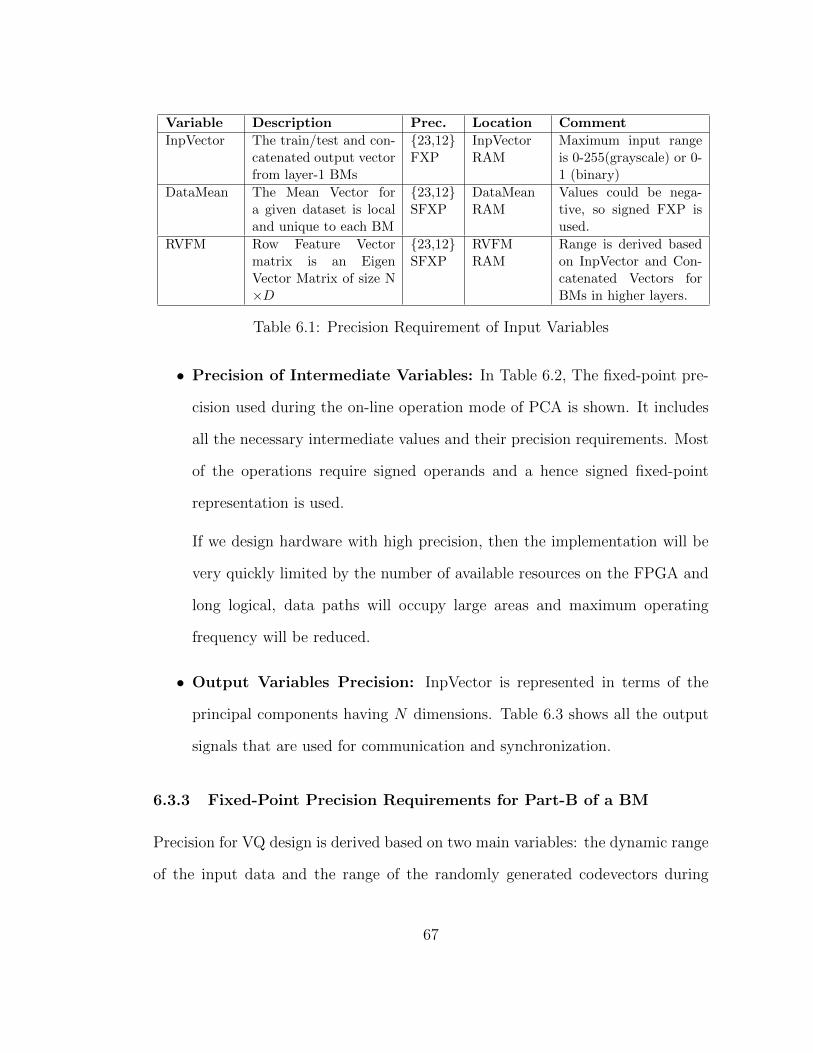
Variable Description Prec. Location Comment
InpVector The train/test and con-catenated output vectorfrom layer-1 BMs
{23,12}FXP
InpVectorRAM
Maximum input rangeis 0-255(grayscale) or 0-1 (binary)
DataMean The Mean Vector fora given dataset is localand unique to each BM
{23,12}SFXP
DataMeanRAM
Values could be nega-tive, so signed FXP isused.
RVFM Row Feature Vectormatrix is an EigenVector Matrix of size N×D
{23,12}SFXP
RVFMRAM
Range is derived basedon InpVector and Con-catenated Vectors forBMs in higher layers.
Table 6.1: Precision Requirement of Input Variables
• Precision of Intermediate Variables: In Table 6.2, The fixed-point pre-
cision used during the on-line operation mode of PCA is shown. It includes
all the necessary intermediate values and their precision requirements. Most
of the operations require signed operands and a hence signed fixed-point
representation is used.
If we design hardware with high precision, then the implementation will be
very quickly limited by the number of available resources on the FPGA and
long logical, data paths will occupy large areas and maximum operating
frequency will be reduced.
• Output Variables Precision: InpVector is represented in terms of the
principal components having N dimensions. Table 6.3 shows all the output
signals that are used for communication and synchronization.
6.3.3 Fixed-Point Precision Requirements for Part-B of a BM
Precision for VQ design is derived based on two main variables: the dynamic range
of the input data and the range of the randomly generated codevectors during
67

Variable Description Prec. Location Comment
Data Ad-just Block
The mean is subtractedfrom the new InpVector
{23,12}SFXP
Subtractor All intermediate vari-ables in this block rangefrom 0-22 bits max.
Result 1 It is the output valuegenerated by the sub-traction unit
{23,12}SFXP
Input toMAC
Value is sign extendedwith the MSB being thesign bit.
RVFM Row Feature Vectormatrix is an EigenVector Matrix of size N×D.
{23,12}SFXP
RVFMRAM
Range is derived basedon InpVector and Con-catenated Vectors forBMs in higher layers.
Mult 1 Result of multiplica-tion:mult 1 = RVFM×DataAdjV ector
{46,0}SFXP
MAC: Mul-tiply Unit
It is the intermediatevalue generated by mul-tiplication of the RFVMand mean adjusted In-pVector.
Mult 2 Selecting required num-ber of bits from mult 1.[Mult 2 =mult 1[45:12]]
{33,0}SFXP
MAC: Mul-tiply Unit
By truncating the leastsignificant bits only 33bits are stored. Sign ispreserved.
PCA Vectorinternal
Only 23 bits necessaryto represent the com-puted value are accumu-lated with previous re-sult.
{23,12}SFXP
MAC: Mul-tiply Unit
The maximum range isderived based on the in-puts it receives and thedesired output width.
N bit AdderBlock
It performs signed addi-tion of two 23 bit num-bers it receives frommultiply unit.
{23,12}SFXP
MAC:AdderBlock
Intermediate valueshave the same preci-sion as input/outputvariables of the adderblock.
Table 6.2: Precision Requirement of Intermediate Variables
68

Variable Description Prec. Location Comment
FinalV ector(FV)
Projected InpVectorinto an Eigen spacewith first N principalcomponents.
{23,12}SFXP
part-A:Output
Each element in the FVhas the same Prec. Thelength of FV is [1×N ].
R1 avail Indicates completion ofsubtract operation tothe controller.
{1,0} part-A:Outputsignal
Control signal.
FVi avail Final vector availablesignal. Connects to thecontroller.
{1,0} part-A:Outputsignal
Control signal.
Table 6.3: Precision Requirement of Output Variables
initialization. Fixed-Point Precision analysis for VQ can be divided into 3 sections
based on the variables being used as an input, for intermediate results and final
outputs of the circuit.
• Precision of Input Variables
Table 6.4 lists all the input variables required by VQ and their precision
settings. The precision (Prec.) is represented by {P,Q} notation in which P
is the number of bits used to represent the digits to the left of the binary
point (decimal component); while Q is the number of bits used to represent
the digits to the right of the binary point (fractional component).
• Precision of Intermediate Variables Training/learning is an iterative
process and all the variables which are modified during this process needs
to be carefully observed before defining their precision requirements. The
iterative process was done in the MATLAB and the dynamic range for each
variable was determined. Table 6.5 shows all the intermediate variables that
are modified in this iterative process.
• Precision of Output Variables The output of part-B is the index of the
69

Variable Description Prec. Location Comment
FinalVectorFVi
Train and Test vectorfor VQ circuit of BMs.
{23,12}SFXP
FIFO RAM It is the projection ofInpVector into an Eigenspace with N principalcomponents.
CodevectorCBi
Each row of the Code-book represents a code-vector of N elements.
{23,12}SFXP
CodebookRAM
Initialized under con-trolled conditions toavoid underflow oroverflow.
LearningRate (α)
α is defined at the cir-cuit initialization and isa constant value.
{23,12}FXP
UpdateBlock
”Learning Rate” is aconstant variable.
Table 6.4: Precision Requirement of Input Variables (part-B)
winner distance computed by performing a linear search through the dis-
tances corresponding to each codevector in the Codebook. The winning
index is used to point to the codevector in order to form the concatenated
vector along with the adjacent winning codevectors from neighboring BMs.
The concatenated vector acts as an InpVector to the BMs in the upper layers.
Table 6.6 shows the precision settings for output variables of part-B.
70

Variable Description Prec. Location Comment
SubtractorBlock
Difference is calculatedbetween two points andthe result is the distancebetween the points inthe current dimensionof space.
{24,0}FXP
SubtractorBlock
All intermediate vari-ables in this block rangefrom 0-23 bits max.
sub val Difference betweenFViandcodevector(FVi)
{23,12}FXP
Input tonBitAdderBlock
It is an absolute valueand gets added to previ-ous difference values ofFV and CV.
Codevector(CV)
codevector (centroids)is N dimensional andeach element has thesame precision.
{23,12}SFXP
CodebookRAM
α and Epoch size af-fect the precision of CV .The initial values followthe same precision.
Diff val(ac tmp 1)
It is the difference valuebetween FViandFVi.
{24,12}SFXP
UpdateBlock
Intermediate result gen-erated by Subtractor.Sign bit is the MSB andhence 24 bits.
Multiply val(ac tmp 2)
The result of multiply-ing diff val by α.
{48,0}SFXP
UpdateBlock
diff val in the last stepis multiplied by thelearning rate to update(increment) the weightvalue.
Sign adjust 1(step1)
Only the sign bit is for-warded and the remain-ing MSB bits are dis-posed.
{35,0}SFXP
UpdateBlock
Register size is decidedby the operands. Usu-ally twice the width ofinput variables.
Addition val(ac tmp 12)
This is the new updatedvalue of codevector’s el-ement.
{45,0}SFXP
UpdateBlock
It is the output ofadding new updatedvalue with old value ofcodevectors element.
Updatedcodevectorval
In order to maintainthe constant bit lengthfor codevector elements,LSB bits of addition valare disposed.
{23,12}SFXP
UpdateBlock
Without losing pre-cision, this range isdecided based on theMATLAB and RTLfunctional model.
Table 6.5: Precision Requirement of Intermediate Variables
71

Variable Description Prec. Location Comment
Updatedcodevectorval
In order to maintainthe constant bit lengthfor codevector elements,LSB bits of addition valare disposed off.
{23,12}SFXP
UpdateBlock
Without losing preci-sion from the first it-eration to last iterationthis range has been de-cided.
Mi (Min-imumIndex)
Index value. {5,0}FXP
finalDminIndex Block
The index value corre-sponding to the code-vector that is closestto the given input vec-tor. The range mayvary based on the size ofCB.
Mi avail(indexavail)
Indicates completion oflinear search throughthe distance table.
{1,0} part-B:Outputsignal
Control signal.
Updatedcodevectoravail
Updated codevector el-ement available signal.Connects to the con-troller.
{1,0} part-B:Outputsignal
Control signal.
Table 6.6: Precision Requirement of Output Variables
72

Chapter 7
Results & Analysis
The BM architecture explained in Chapter 6 was implemented using the procedures
and tools described in Chapter 5. Here we discuss the verification of our design,
the performance results of a BM architecture followed by a brief analysis and
discussion of the results.
7.1 Design Verification Methodology
The reference design of the Hierarchical Character Recognition System was im-
plemented in MATLAB with FLP precision and FXP MATLAB model was de-
veloped to verify the Verilog simulations and FPGA results. The tables 7.1, 7.2
and 7.3 shows the sample outputs for each of the computational units within
the BM. The main columns in each table represents inputs to the and output
of that block; subcolumns represent, ‘FLP’ Floating Point MATLAB model re-
sults, ‘FXP’ Fixed Point MATLAB model results and ‘Verilog’, i.e., results ob-
tained from Verilog simulation model. It was discussed earlier that how a number
in FLP precision is represented with limited FXP precision. Simulation wave-
forms confirm the functionality of the individual blocks as the Verilog simula-
tion results match with the FXP MATLAB model and FXP MATLAB model
results match with the base FLP MATLAB model. The values seen in the wave-
forms and in that of the tables are the same and hence the design is function-
ally correct. Waveforms for each sub block of part-A are shown in Figure 7.1,7.2
73

Figure 7.1: Waveforms for the DataAdj Block
and 7.3. Figures 7.4 and 7.5 show simulations for part-B of BM. The simula-
tions are shown for N = 4, Iterations = 1, CB = 25, RV FM = [4 × 16] and
DVM = [1 × 16], Clock = 50MHz. Keeping the clock speed constant, system
performance can be further improved by adding parallelism within the BM node.
While the results here are only from single iteration, the design was tested for the
entire train and test dataset of 11000 images.
Data Mean Input Vector Data Adjust Block
FLP FXP Verilog FLP FXP Verilog FLP FXP Verilog
0 0 0 0 0 0 0 0 0
0.0427 174 174 1 4096 4096 0.9575 3992 3992
0.0781 320 320 1 4096 4096 0.9219 3776 3776
0.116 475 475 1 4096 4096 0.884 3621 3621
0.1634 669 669 1 4096 4096 0.8366 3427 3427
0.0884 362 362 0 0 0 -0.0884 -362 -362
Table 7.1: Verification Data for Data Adjust Block
Row Feature Vector MAC
FLP FXP Verilog FLP FXP Verilog
0.0551 225 225 1.7292 7083 7083
-0.1418 -581 -581 -1.0574 -4331 -4331
0.128 524 524 1.1697 4791 4791
-0.2285 -936 -936 -0.1108 -454 -454
Table 7.2: Verification Data for MAC Unit
74

Figure 7.2: Waveforms for Row Feature Vector Matrix
Figure 7.3: Waveforms for MAC Unit
Codebook Vectors Subtractor Output Distances
FLP FXP Verilog FLP FXP Verilog FLP FXP Verilog
2.5759 10551 10551 0.8467 3468 3468 2.9023 11888 11888
-0.8379 -3432 -3432 0.2195 899 899 2.8494 11671 11671
0.1189 487 487 1.0508 4304 4304 3.6846 15092 15092
-0.8962 -3671 -3671 0.8672 3217 3217 4.3943 17999 17999
1.978 8102 8102 0.2488 1019 1019 4.7917 19627 19627
Table 7.3: Verification Data for Subtractor, Codebook Distances
Figure 7.4: Simulation Waveforms for Codebook Vectors
Figure 7.5: Simulation Waveforms for Subtractor
Minimum Index value
FLP FXP Verilog
12 11 11
1 0 0
14 13 13
Table 7.4: Verification Data for MinimumIndex Search Block
75

Please note that the minimum index value obtained in Verilog is one less than
the MATLAB values, since memory accesses starts with zero. So if the Minimum
index is ‘1’ in MATLAB that means it is the codevector whose start address is
0×00 in the Codebook.
The results shown above are for binary representation of input images but the
precision range allows us to have raw input images, i.e., grayscale images directly
as the network’s input. The design was tested for grayscale images as well and
produced desired results.
7.2 Performance Evaluation
7.2.1 Speedup
Here we discuss the estimated degree of speedup that the FPGA implementation
can provide against the MATLAB algorithm running on a 2.1 GHz Intel Core-2
duo computer.
Performance/Hardware analysis of the hierarchical network consisting of several
BMs can be derived from the characteristics of a single BM’s performance and
response time. The response time is defined as the time from which the BM
is presented with an input pattern to the time it produces an output for that
particular input pattern.
Pipelining the design as shown in the Figure 7.6 allows us to run the design at
higher frequencies. The obvious drawback is that the design takes more than one
clock cycle to perform the operation. The values are registered at every stage in
the pipeline. If the design is achieved using more combinational logic, it puts the
limit on the maximum operating frequency.
76

Figure 7.6: Pipelined Architecture
In the pipelined architecture shown in Figure 7.6, it takes only 3 clock cycles
to access any value from the memory and just one clock cycle to perform the
desired operation. For example to perform the 23-bit multiplication, the controller
takes 3 clock cycles to fetch operands from memory to the multiplier block and
the multiplication is done in just 1 clock cycle. Operating at 50 MHz (t = 20ns),
it can be calculated that the total time to perform the multiplication is (3 + 1)×
(t)ns = 80ns. Similarly, the time required to update an entry in the CodeBook
and time to find the winning index in the test mode can be found out by following
algebraic expressions. The BM module is currently implemented using the Spartan
3E FPGA board. A single module has parameters as shown in Table 7.5.
To estimate the speedup, we formulate the equations for the response and up-
date time of each block and for the complete BM module based on the time period
of the system clock and clock cycles per computation from the Verilog simulation
model. To maintain the consistency, time period of the Verilog simulated model
was set to 20ns and synthesized FPGA model runs on a 50 MHz clock. Following
77

equations are derived for the BM configuration in Table 7.5.
Parameters CBSize
‘N’ Epochs RVFMRAM
DVMRAM
LearningRate (’α’)
Multiplier(for randominit of CB)
Layer =1 25 4 10 [4×16] [1×16] 0.01 10*randBM = (1,1)
Table 7.5: BM Single Module Parameters
Rt1 = 16× (3 + 1)× 20(ns) (7.1)
Rt2 = 16× 4× (4− 1)× 20(ns) (7.2)
Equations 7.1 and 7.2 give us the individual response times for Data Adjust
Block and Multiply Accumulate Unit of part-A of the BM. Similarly, equations
7.3 and 7.9 are for the response and update time calculations of the VQ block.
Update time (TUPDATE) is the sum of total response time (RTOTAL) and the time
it takes to write back the updated values to the block RAMs.
Rt3 = [4× (3 + 1)× 25× 20](ns) (7.3)
RTOTAL = [Rt1 +Rt2 +Rt3](ns) (7.4)
TUPDATE = [RTOTAL + [4× 3× 20]](ns) (7.5)
It is necessary to generalize these equations further to estimate the response
time of the complete hierarchical network with several BMs connected together.
78

The parameters that vary in the above expressions are ‘N ′ and CBi. We can safely
take the time period ‘t′ as a constant for a given design. BMs in the same layer,
running in parallel will have the same response time, the number of BMs that can
run in parallel is dependent on the available logic resources on the given FPGA
device. So our calculation for a single BM can be extended to a hierarchical model
by replacing N and CBi with respect to different layer.
Rt1 = [D × (3 + 1)× t](ns) (7.6)
Rt2 = [D × 4× (N − 1)× t](ns) (7.7)
Rt3 = [N × (3 + 1)× CBi × t](ns) (7.8)
TUPDATE = [RTOTAL + [N × 3× t]](ns) (7.9)
For a BM, the part-A and part-B calculations do not overlap. Also, internal
handshaking avoids contention and data loss. Parallelizing the logic blocks of the
BM will shorten its response time and the execution speed of the entire hierar-
chical system. However, that would be costly in terms of multi-ported BRAMs
and additional data paths on chip. Table 7.6 summarizes the FPGA Speedup
over the MATLAB simulation time for Response/Update Times of the BM. The
total response time RTOTAL for the MATLAB FLP model is calculated using the
stopwatch timer in the MATLAB.
79

Total number of BMs MATLAB RTOTAL FPGA RTOTAL
1 19240000 ns 13030 nsN instances N ×19240000ns 13030 ns
Table 7.6: Response time Speedup
Total number of BMs MATLAB RTOTAL FPGA RTOTAL
1 19240000 ns 13270 nsN instances N ×19240000ns 13270 ns
Table 7.7: Update Time Speedup
7.2.2 Price (Area)
A single BM for the configuration defined in the Table 7.5, utilizes approximately
25 % of the total logic resources available in the FPGA. It provides us with an
opportunity to parallelize the design and run more BMs in parallel. Table 7.8
shows the synthesis results for two BMs running in parallel.
Device Utilization Summary (estimated values)Logic Utilization Used Available UtilizationNumber of Slices 2644 4656 56%Number of Slice Flip Flops 2612 9312 28%Number of 4 input LUTS 4092 9312 43%Number of bonded IOBs 25 232 10%Number of BRAMs 4 20 20%Number of MULT18X18SIOs 8 20 40%Number of GCLKs 4 24 16%
Table 7.8: Synthesis Results for two BMs
For a given FPGA, we were able to run five BMs in parallel. The near-maximum
utilization causes routing delays in the design which directly affects the maximum
clock frequency at which the device can be operated.
Comparing the number of neurons simulated when a single BM is instantiated
and how parallelization at Module level will effectively increase the total number
80

of neurons simulated is summarized by the plot in the Figure 7.7.
1 2 3 4 5 6 70
20
40
60
80
100
120
140
160
180
200
No. of BMI Modules in Parallel
Tota
l n
o. of
Ne
uro
ns S
imula
ted
on F
PG
A
Neurons
Figure 7.7: Number of Neurons Simulated w.r.t the number of BM Modules
Also, the area utilization in terms of Look-up tables (LUT), Flip Flops (FF)
and Block RAMs (BRAM) can be estimated for up to 100 neurons running in
parallel at any given time. The estimated utilization is as shown in Figure 7.8.
20 30 40 50 60 70 80 90 1000
10
20
30
40
50
60
70
80
90
100
No. of Neurons Simulated (#)
Re
sourc
e U
tiliz
atio
n (
%)
LUT
Flip−Flops
BRAM
Figure 7.8: FPGA Resource Utilization w.r.t the number of Simulated Neurons
81

Newer FPGA devices are densely packed and therefore offers more logic re-
sources. The Xilinx-Virtex series has almost the 3x capacity as compared to the
Spartan series. A single BM consumes approximately 1350 slices so depending on
the capacity of the Virtex series FPGAs, more BMs are made to run in parallel
thus increasing the speedup of the entire system.
7.2.3 Hardware Virtualization
FPGA based designs for biologically inspired computational models are dominated
by the available chip area and logic resources. To best utilize the available logic re-
sources, classic space-time trade off is made and for hardware designs it is known
as hardware virtualization. “The degree of time-multiplexing of the computa-
tional blocks and communication, i.e., address/data buses via hardware resources
is defined as the hardware virtualization” [1], [3]. An example from our design is
discussed to understand the application of hardware virtualization in our design.
In the training phase, the winning codevector is updated on every iteration.
An Update Logic block in the part-B does the job of updating the codevector.
Depending on the codevector length, the update operation is performed for each
element in the codevector. Figure 7.9 shows how hardware resources can be vir-
tualized to take full advantage of the given logic resources without degrading the
overall system performance.
The minimal virtualization shown in Figure 7.9 (a) is the fastest of the three
implementations, but also the most expensive in terms of its area on chip and
logic resource utilization. The time-multiplexing of available UpdateLogic blocks
is demonstrated in Figure 7.9 (b) & (c). Figure 7.9 (c) shows the maximum limit
of h/w virtualization by sacrificing the speed, as this design is the slowest of the
82

Figure 7.9: Virtualization of hardware resources: Update Logic
three, but it consumes the least area and is the cheapest in terms of logic resource
utilization amongst the three designs. Therefore, it is observed that the degree of
hardware virtualization for a given design can be varied by varying the assignment
of available logic resources based on the performance/price trade-offs.
Figure 7.6 exploits the virtualization at the layer level by instantiating a lim-
ited number of BM modules and time-multiplexing them to effectively realize the
functionality of the complete layer.
The FPGA offers dense interconnect structure, so with all the optimizations
throughout the design it is not possible to utilize the 100% resources. As the design
83

becomes more complex, it affects the maximum operating frequency because of the
routing delays and wiring overhead and could soon limit the network size. Figure
7.10 shows the effects of scaling, 4 BM Modules in running in parallel the operating
frequency, best case operating frequency and slack as a timing concern. Slack is
defined as the amount of time you have that is measured from when an event
‘actually happens’ and when it ‘must happen’. Negative slack implies that the
‘actually happen’ time is later than the ‘must happen’ time, in other words it’s
too late and it’s a timing violation. Actual frequency is the 50MHz clock and
is constant for the design. Best case achievable frequency is obtained from the
synthesis report and changes based on the device logic resource utilization.
1 2 3 40
5
10
15
20
25
BMI Modules in Parallel
Maxim
um
Tim
e P
eriod (
ns)
Slack Best Case Actual
Figure 7.10: Effect of Parallelization on Slack and Best Achievable Frequency
7.3 Conclusion
The thesis proposes a Bayesian Memory which is an approximation to the HTM
node. Here we have shown how the Principal Component Analysis can be used
84

as one of the optimization techniques to make FPGA implementation of such
biologically inspired computing algorithms possible. Advantages of using the PCA
are:
The PCA technique itself does not require significant logic resources for its
hardware implementation.
The number of Epochs is reduced to tens as against 100s to 1000s for only
VQ based BM design. Even with the maximum number of Principal Components,
the Codebook size does not exceed the available Block RAMs on chip and makes
FPGA implementation practical.
The fewer Epochs, FXP precision requirements go down and the complete BM
design is achieved with 23 bit precision. The FXP multiplication unit is custom
designed for the defined FXP precision and hence can be used as it is for other
designs with same precision settings.
Preserving only the 1/4th dimensions at all the layers, the classification accu-
racy of the network is still above or close to 90% which is a good indicator that
this technique is effective and can be used in the future designs.
Speedup was evaluated by deriving the response and update time equations.
The FPGA implementation is 1000x faster over MATLAB implementation. It
shows that, FPGAs can be used for real-time recognition applications built out of
these algorithms.
A single BM module, as presented here, occupies approximately 25% of the logic
resources of a 500k Spartan 3E FPGA device. For higher end FPGAs, more BM
modules can be synthesized for performance improvement of the overall system.
The best achievable operating frequency for a single BM was observed to be 110
MHz which is 2x faster than the existing clock speed.
85

The RTL developed is highly modularized and parametrized, can be easily
extended for varying network sizes.
7.4 Future Work
• More functionality like temporal pooling could be added to the existing BM
design. Possible hardware optimization and acceleration techniques for the
same can be explored.
• In our RTL design the inter-layer communication can be established and a
sub-network with 2 child BMs and one parent BM can be synthesized. Also
taking it further, now this structure with 3 BMs can be parallelized and
throughput can be calculated by equations presented in this work.
• Soft processor cores such as PicoBlaze or MicroBlaze can be added to the
design in order to use FPGA as an hardware acceleration adapter for the
PC based software simulation. It would be an interesting exercise to find
out whether communication overhead for this scheme significantly affects
the performance as against using only FPGA for complete operation.
• Hardware Virtualization, i.e., space-time trade-off for hardware designs dis-
cussed in this work can be extended to perform the power performance anal-
ysis for ASIC based designs. This analysis will be very helpful for present as
well as future implementations, as the chip area is becoming smaller and more
logic is being added at the same time, thermal power plays an important role
in any ASIC design.
• A special on-chip communication bus could to be developed which can handle
86

data and addresses efficiently and lower logic resource utilization of the target
FPGA device.
87

References
[1] A. Bermak and D. Martinez. A compact 3d vlsi classifier using bagging thresh-
old network ensembles. Neural Networks, IEEE Transactions on, 14(5):1097
– 1109, sep. 2003.
[2] A. Das, S. Misra, S. Joshi, J. Zambreno, G. Memik, and A. Choudhary. An
efficient fpga implementation of principle component analysis based network
intrusion detection system. pages 1160 –1165, mar. 2008.
[3] Changjian Gao and D. Hammerstrom. Cortical models onto cmol and cmos
x2014; architectures and performance/price. Circuits and Systems I: Regular
Papers, IEEE Transactions on, 54(11):2502 –2515, nov. 2007.
[4] Changjian Gao, M.S. Zaveri, and D. Hammerstrom. Cmos / cmol architec-
tures for spiking cortical column. In Neural Networks, 2008. IJCNN 2008.
(IEEE World Congress on Computational Intelligence). IEEE International
Joint Conference on, pages 2441 –2448, 2008.
[5] D. George and J. Hawkins. A hierarchical bayesian model of invariant pattern
recognition in the visual cortex. volume 3, pages 1812 – 1817 vol. 3, jul. 2005.
[6] D. George and J. Hawkins. A hierarchical bayesian model of invariant pattern
recognition in the visual cortex. volume 3, pages 1812 – 1817 vol. 3, jul. 2005.
[7] A. Gresho and R. M. Gray. Vector Quantization and Signal Compression.
MA: Kluwer Academic Publishers, Norwell, 1991.
88

[8] Dan Hammerstrom. A survey of bio-inspired and other alternative architec-
tures. Wiley-VCH Verlag GmbH Co. KGaA, 2010.
[9] Dan Hammerstrom and Mazad Zaveri. Bayesian memory, a possible hardware
building block for intelligent systems. volume FS-08-04, pages 81 –, Arlington,
VA, United states, 2008.
[10] J. Hawkins. Why can’t a computer be more like a brain? Spectrum, IEEE,
44(4):21 –26, apr. 2007.
[11] J. Hawkins and S. Blakeslee. On Intelligence. Henry Holt and Company, New
York, NY: Times Books,, 2004.
[12] S. Haykin. Neural Networks: A Comprehensive Foundation. New Delhi: Pren-
tice Hall of India, 2nd ed, 1998.
[13] IEEE. Ieee standard verilog hardware description language. IEEE Std 1364-
2001, pages 0–856, 2001.
[14] Intel. 60 years of the transistor: 1947-2007.
http://www.intel.com/technology/timeline.pdf, 2007.
[15] Rinkus Gerard J. A cortical sparse distributed coding model linking mini- and
macrocolumn-scale functionality. Frontiers in Neuroanatomy, (0):12, 2010.
[16] V. Mountcastle. Perceptual Neuroscience - The Cerebral Cortex. MA: Harvard
University Press, Cambridge, 1998.
[17] Amos R. Omondi and Jagath C. Rajapakse. FPGA Implementations of Neural
Networks. Springer-Verlag New York, Inc., Secaucus, NJ, USA, 2006.
89

[18] S. Rowies. USPS Handwritten Digits Database.
http://www.cs.toronto.edu/ roweis/data.html, 2009.
[19] Xilinx. Acceldsp synthesis tool floating-point to fixed-point conversion of
matlab. White paper, Xilinx, 2006. White Paper.
90