gp88s portable radio - myradio168.net · viii safety information operational warnings operational...
TRANSCRIPT

November, 2003
GP88sPortable Radio
Service Manual
6804111J47-D

Computer Software Copyrights
The Motorola products described in this manual may include copyrighted Motorola computer programs stored in semiconductor memories or other media. Laws in the United States and other countries preserve for Motorola certain exclusive rights for copyrighted computer programs, including the exclusive right to copy or reproduce in any form, the copyrighted computer program. Accordingly, any copyrighted Motorola computer programs contained in the Motorola products described in this manual may not be copied or reproduced in any manner without the express written permission of Motorola. Furthermore, the purchase of Motorola prod-ucts shall not be deemed to grant, either directly or by implication, estoppel or otherwise, any license under the copyrights, patents or patent applications of Motorola, except for the normal non-exclusive royalty-free license to use that arises by operation of law in the sale of a product.

Document History iii
Document History
The following major changes have been implemented in this manual since the previous edition:
Edition Description Date
6804111J47-D Updated the mechanical parts list and exploded view. Nov. 2003

iv Document History
THIS PAGE INTENTIONALLY LEFT BLANK

Safety Information v
SAFETY INFORMATION
Product Safety and RF Exposure for Portable Two-Way Radios
The information provided in this document supersedes the general safety information contained in user guides published prior to February 2002.
For radios that have been approved as intrinsically safe, read the instructions and information on intrinsic safety.
Compliance with RF Energy Exposure StandardsNOTICE: This radio is intended for use in occupational/controlled applications where users
have been made aware of the potential for exposure and can exercise control over their exposure. This radio device is NOT authorized for general population, consumer or similar use.
Federal Communication Commission(FCC) RegulationsThe FCC has established limits for safe exposure to radio frequency (RF) emissions from portable two-way radios. The FCC requires manufacturers to demonstrate compliance with RF exposure limits before portable two-way radios can be marketed in the U.S. When two-way radios are approved for occupational/controlled environment exposure limits, the FCC requires users to be fully aware of, and exercise control over, their exposure. Awareness and control of RF exposure can be accomplished by the use of labels, or by education or training through appropriate means, such as information and instructions in user manuals or safety booklets.
Your Motorola two-way radio has an RF exposure information label in the battery compartment. This user safety booklet includes useful information about RF exposure and helpful instructions on how to control your RF exposure.
Your Motorola two-way radio is designed and tested to comply with a number of national and international standards and guidelines (listed below) regarding human exposure to radio frequency electromagnetic energy. This radio complies with the IEEE (FCC) and ICNIRP exposure limits for occupational/controlled RF exposure environments at usage factors of up to 50% talk–50% listen. In terms of measuring RF energy for compliance with FCC exposure guidelines, your radio radiates measurable RF energy only while it is transmitting (during talking), not when it is receiving (listening) or in standby mode.
NOTE:The approved batteries, supplied with the portable radio, are rated for a 5-5-90 duty cycle (5% talk–5% listen–90% standby), even though this radio complies with FCC occupational exposure limits at usage factors of up to 50% talk.
Your Motorola two-way radio complies with the following RF energy exposure standards and guidelines:
• United States Federal Communications Commission, Code of Federal Regulations; 47 CFR part 2 sub-part J
• American National Standards Institute (ANSI) / Institute of Electrical and Electronic Engineers (IEEE) C95. 1-1992
• Institute of Electrical and Electronic Engineers (IEEE) C95.1-1999 Edition• International Commission on Non-Ionizing Radiation Protection (ICNIRP) 1998
BEFORE USING THIS RADIO, READ THIS BOOKLET WHICH CONTAINS IMPORTANT OPERAT-ING INSTRUCTIONS FOR SAFE USAGE AND RF ENERGY AWARENESS AND CONTROL INFOR-MATION FOR COMPLIANCE WITH RF ENERGY EXPOSURE LIMITS IN APPLICABLE NATIONAL AND INTERNATIONAL STANDARDS.

vi Safety Information
• Ministry of Health (Canada) Safety Code 6. Limits of Human Exposure to Radiofrequency Elec-tromagnetic Fields in the Frequency Range from 3 kHz to 300 GHz, 1999
• Australian Communications Authority Radiocommunications (Electromagnetic Radiation - Human Exposure) Standard, 2001
• ANATEL, Brasil Regulatory Authority, Resolution 256 (April 11, 2001) “additional requirements for SMR, cellular and PCS product certification.”
Compliance and Control Guidelines and Operating Instructions for Portable Two-Way Radios
To control your exposure and ensure compliance with the occupational/ controlled environment exposure limits, always adhere to the following procedures:
• Transmit no more than 50% of the time. To transmit (talk), push the Push-To-Talk (PTT) button. To receive calls, release the PTT button. Transmitting 50% of the time or less is important since the radio generates measurable RF energy exposure only when transmitting (in terms of measuring standards compliance).
• Hold the radio in a vertical position in front of the face with the microphone (and other parts of the radio including the antenna) at least one to two inches (2.5 to 5 centimeters) away from the lips. Keeping the radio at a proper dis-tance is important since RF exposures decrease with distance from the antenna.
• For body-worn operation, always place the radio in a Motorola-approved clip, holder, holster, case, or body harness for this product. Using non–Motorola-approved accessories may result in exposure levels which exceed the FCC’s occupational/controlled environment RF exposure lim-its.
• If you are not using a body-worn accessory and are not using the radio in the intended use posi-tion in front of the face, ensure the antenna and the radio are kept one inch (2.5 centimeters) from the body when transmitting. Keeping the radio at a proper distance is important since RF exposures decrease with distance from the antenna.
• Use only Motorola-approved supplied or replacement antennas, batteries, and accesso-ries. Use of non–Motorola-approved antennas, batteries and accessories may exceed FCC RF exposure guidelines. For a list of Motorola-approved antennas,batteries, and other acces-sories, visit the following web site which lists approved accessories: http://ap.cgiss.motorola.com/AAD/index.html
For additional information on exposure requirements or other training information, visit http://www.motorola.com/rfhealth.
Electromagnetic Interference/CompatibilityNOTE:Nearly every electronic device is susceptible to electromagnetic interference (EMI) if
inadequately shielded, designed, or otherwise configured for electromagnetic compatibility.
FacilitiesTo avoid electromagnetic interference and/or compatibility conflicts, turn off your radio in any facility where posted notices instruct you to do so. Hospitals or health care facilities may be using equipment that is sensitive to external RF energy.
AircraftWhen instructed to do so, turn off your radio when on board an aircraft. Any use of a radio must be in accordance with applicable regulations per airline crew instructions.

Safety Information vii
Medical Devices
Pacemakers
The Advanced Medical Technology Association (AdvaMed) recommends that a minimum separation of 6 inches (15 centimeters) be maintained between a handheld wireless radio and a pacemaker. These recommendations are consistent with those of the U.S. Food and Drug Administration.
Persons with pacemakers should:
• ALWAYS keep the radio more than 6 inches (15 centimeters) from their pacemaker when the radio is turned ON.
• not carry the radio in the breast pocket.• use the ear opposite the pacemaker to minimize the potential for interference.• turn the radio OFF immediately if you have any reason to suspect that interference is taking
place.
Hearing Aids
Some digital wireless radios may interfere with some hearing aids. In the event of such interference, you may want to consult your hearing aid manufacturer to discuss alternatives.
Other Medical Devices
If you use any other personal medical device, consult the manufacturer of your device to determine if it is adequately shielded from RF energy. Your physician may be able to assist you in obtaining this information.
Driver SafetyCheck the laws and regulations on the use of radios in the area where you drive. Always obey them.
When using your radio while driving, please:
• Give full attention to driving and to the road.• Use hands-free operation, if available.• Pull off the road and park before making or answering a call if driving conditions so require.

viii Safety Information
Operational Warnings
Operational Cautions
Intrinsically Safe Radio Information
FMRC Approved EquipmentAnyone intending to use a radio in a location where hazardous concentrations of flammable materials exist (hazardous atmosphere) is advised to become familiar with the subject of intrinsic safety and with the National Electric Code NFPA 70 (National Fire Protection Association) Article 500 (hazardous [classified] locations).
An Approval Guide, issued by Factory Mutual Research Corporation (FMRC), lists manufacturers and the products approved by FMRC for use in such locations. FMRC has also issued a voluntary approval standard for repair service (“Class Number 3605”).
FMRC Approval labels are attached to the radio to identify the unit as being FMRC Approved for specified hazardous atmospheres. This label specifies the hazardous Class/Division/Group along with the part number of the battery that must be used. Depending on the design of the portable unit, this FM label can be found on the back or the bottom of the radio housing. The FM Approval Mark is shown here.
For Vehicles With An Air BagDo not place a portable radio in the area over an air bag or in the air bag deployment area. Air bags inflate with great force. If a portable radio is placed in the air bag deployment area and the air bag inflates, the radio may be propelled with great force and cause serious injury to occupants of the vehicle.
Potentially Explosive AtmospheresTurn off your radio prior to entering any area with a potentially explosive atmosphere, unless it is a portable radio type especially qualified for use in such areas as “Intrinsically Safe” (for example, Factory Mutual, CSA, UL, or CENELEC). Do not remove, install, or charge batteries in such areas. Sparks in a potentially explosive atmosphere can cause an explosion or fire resulting in bodily injury or even death.The areas with potentially explosive atmospheres referred to above include fueling areas such as below decks on boats, fuel or chemical transfer or storage facilities, and areas where the air contains chemicals or particles such as grain, dust or metal powders. Areas with potentially explosive atmospheres are often, but not always, posted.
Blasting Caps And Blasting AreasTo avoid possible interference with blasting operations, turn off your radio when you are near electrical blasting caps, in a blasting area, or in areas posted: “Turn off two-way radio.” Obey all signs and instructions.
AntennasDo not use any portable radio that has a damaged antenna. If a damaged antenna comes into contact with your skin, a minor burn can result.
BatteriesAll batteries can cause property damage and/or bodily injury such as burns if a conductive material such as jewelry, keys, or beaded chains touch exposed terminals. The conductive material may complete an electrical circuit (short circuit) and become quite hot. Exercise care in handling any charged battery, particularly when placing it inside a pocket, purse, or other container with metal objects.
FM
APPROVED

Safety Information ix
Radios must ship from the Motorola manufacturing facility with the hazardous atmosphere capability and FM Approval labeling. Radios will not be “upgraded” to this capability and labeled in the field. A modification changes the unit’s hardware from its original design configuration. Modifications can only be made by the original product manufacturer at one of its FMRC-audited manufacturing facilities.
Repair of FMRC Approved ProductsREPAIRS FOR MOTOROLA PRODUCTS WITH FMRC APPROVAL ARE THE RESPONSIBILITY OF THE USER.
You should not repair or relabel any Motorola-manufactured communication equipment bearing the FMRC Approval label (“FMRC Approved Product”) unless you are familiar with the current FMRC Approval standard for repairs and service (“Class Number 3605”).
You may want to consider using a repair facility that operates under 3605 repair service approval.
• Do not operate radio communications equipment in a hazardous atmosphere unless it is a type especially qualified (for example, FM Approved) for such use. An explosion or fire may result.
• Do not operate an FMRC Approved product in a hazardous atmosphere if it has been physically damaged (for example, cracked housing). An explosion or fire may result.
• Do not replace or charge batteries in a hazardous atmosphere. Contact sparking may occur while installing or removing batteries and cause an explosion or fire.
• Do not replace or change accessories in a hazardous atmosphere. Contact sparking may occur while installing or removing accessories and cause an explosion or fire.
• Turn the radio off before removing or installing a battery or accessory.• Do not disassemble an FMRC Approved Product in any way that exposes the internal
circuits of the unit.
• Failure to use an FMRC Approved Product with an FMRC Approved battery or FMRC Approved accessories specifically approved for that product may result in the dangerously unsafe condition of an unapproved radio combination being used in a hazardous location.
• Unauthorized or incorrect modification of an FMRC Approved Product will negate the Approval rating of the product.
• Incorrect repair or relabeling of any FMRC Approved Product could adversely affect the Approval rating of the unit.
• Use of a radio that is not intrinsically safe in a hazardous atmosphere could result in serious injury or death.

x Safety Information
The FMRC’s Approval Standard Class Number 3605 is subject to change at any time without notice to you. You may want to obtain a current copy of 3605 from the FMRC. Per the December 1994 publication of 3605, some key definitions and service requirements are as follows:
Repair
A repair constitutes something done internally to the unit that would bring it back to its original condition—Approved by FMRC. A repair should be done in an FMRC Approved repair facility.
Items not considered as repairs are those in which an action is performed on a unit which does not require the outer casing of the unit to be opened in a manner that exposes the internal electrical circuits of the unit. You do not have to be an FMRC Approved repair facility to perform these actions.
Relabeling
The repair facility shall have a method by which the replacement of FMRC Approval labels are controlled to ensure that any relabeling is limited to units that were originally shipped from the manufacturer with an FM Approval label in place. FMRC Approval labels shall not be stocked by the repair facility. An FMRC Approval label shall be ordered from the original manufacturer, as needed, to repair a specific unit. Replacement labels may be obtained and applied by the repair facility, provided there is satisfactory evidence that the unit being relabeled was originally an FMRC Approved unit. Verification may include, but is not limited to a unit with a damaged Approval label, a unit with a defective housing displaying an Approval label, or a customer invoice indicating the serial number of the unit and purchase of an FMRC Approved model.
Do Not Substitute Options or AccessoriesThe Motorola communications equipment certified by Factory Mutual is tested as a system and consists of the FM Approved portable, FM Approved battery, and FM Approved accessories or options, or both. This FM Approved portable and battery combination must be strictly observed. There must be no substitution of items, even if the substitute has been previously Approved with a different Motorola communications equipment unit. Approved configurations are listed in the FM Product Listing Manual that was included with your radio.

xi
Table of Contents
Section SAFETY INFORMATION
Section 1 Introduction
1.0 Scope of Manual.................................................................................................. 1-12.0 Warranty and Service Support............................................................................. 1-1
2.1 Warranty Period and Return Instructions ....................................................... 1-12.2 After Warranty Period..................................................................................... 1-12.3 Piece Parts ..................................................................................................... 1-22.4 Technical Support .......................................................................................... 1-3
3.0 Radio Model Information...................................................................................... 1-4
Section 2 Accessories
1.0 Antennas.............................................................................................................. 2-12.0 Carrying Accessories........................................................................................... 2-13.0 Chargers .............................................................................................................. 2-14.0 Batteries............................................................................................................... 2-15.0 Adaptors .............................................................................................................. 2-16.0 Audio Accessories ............................................................................................... 2-27.0 Option Boards...................................................................................................... 2-28.0 Manuals ............................................................................................................... 2-29.0 Retrofit Kit ............................................................................................................ 2-210.0 Service Kits.......................................................................................................... 2-2
Section 3 Service Aids
1.0 Recommended Test Tools................................................................................... 3-12.0 Service Aids......................................................................................................... 3-23.0 Test Equipment.................................................................................................... 3-34.0 Programming/Test Cable..................................................................................... 3-4
Section 4 Maintenance
1.0 Introduction .......................................................................................................... 4-12.0 Preventive Maintenance ...................................................................................... 4-1
2.1 Inspection ....................................................................................................... 4-12.2 Cleaning Procedures...................................................................................... 4-1
3.0 Safe Handling of CMOS and LDMOS Devices.................................................... 4-24.0 Repair Procedures and Techniques — General.................................................. 4-35.0 Disassembling and Reassembling the Radio — General.................................... 4-4

xii
6.0 Radio Disassembly — Detailed............................................................................4-56.1 Front Cover from Chassis Disassembly .........................................................4-56.2 Chassis Assembly Disassembly .....................................................................4-76.3 Keypad/Option Board Disassembly ................................................................4-86.4 Speaker, Microphone, and Wire Disassembly................................................4-96.5 PTT Disassembly..........................................................................................4-106.6 Control Top Disassembly..............................................................................4-11
7.0 Radio Reassembly — Detailed ..........................................................................4-117.1 Control Top Reassembly ..............................................................................4-117.2 PTT Reassembly ..........................................................................................4-117.3 Speaker Reassembly....................................................................................4-117.4 Keypad Option Board, Microphone and Wire Reassembly ..........................4-127.5 Chassis Assembly Reassembly....................................................................4-127.6 Chassis and Front Cover Reassembly .........................................................4-13
8.0 Option Board Installation....................................................................................4-138.1 Configuring the Radio after Option Board Installation ..................................4-158.2 Additional Configuration required by the DTMF Option Board .....................4-16
9.0 Mechanical View and Parts List .........................................................................4-179.1 GP88s Exploded View and Parts List ...........................................................4-17
Section 5 Transceiver Performance Testing
1.0 Introduction ..........................................................................................................5-12.0 Setup....................................................................................................................5-13.0 Test Mode ............................................................................................................5-2
3.1 RF Test Mode .................................................................................................5-2
Section 6 Radio Tuning And Programming
1.0 Introduction ..........................................................................................................6-12.0 Radio Tuning Setup .............................................................................................6-23.0 CPS Programming Setup.....................................................................................6-34.0 Cloning Information ..............................................................................................6-3
Section 7 Controller Information
1.0 Overview ..............................................................................................................7-12.0 Radio Power Distribution......................................................................................7-13.0 Controller Board ...................................................................................................7-2
3.1 General ...........................................................................................................7-23.2 Digital Architecture..........................................................................................7-33.3 Controller Schematics (403-470MHz for 8480672Z01 & 136-174MHz for
8480675Z01)7-5Complete Controller Schematic Diagram................................................................7-5

xiii
Controller ASFIC/ON_OFF Schematic Diagram .................................................... 7-6Controller Micro Processor Schematic Diagram .................................................... 7-7Controller Memory Schematic Diagram ................................................................. 7-8Controller Audio Power Amplifier Schematic Diagram ........................................... 7-9Controller Interface Schematic Diagram .............................................................. 7-103.4 Controller Schematics (403-470MHz for 8480672Z04, Z06 & 136-174MHz for
8480675Z03, Z04)7-11Complete Controller Schematic Diagram ............................................................. 7-11Controller ASFIC/ON_OFF Schematic Diagram .................................................. 7-12Controller Micro Processor Schematic Diagram .................................................. 7-13Controller Memory Schematic Diagram ............................................................... 7-14Controller Audio Power Amplifier Schematic Diagram ......................................... 7-15Controller Interface Schematic Diagram .............................................................. 7-16
Section 8 Keypad Board Information
1.0 Theory of Operation............................................................................................. 8-12.0 Troubleshooting Chart ......................................................................................... 8-13.0 Parts List (Keypad) .............................................................................................. 8-24.0 Keypad Board And Schematic Diagram .............................................................. 8-3
Keypad Board Top and Bottom View (PCB No. 8485642Z01)............................... 8-3Keypad Board Schematic Diagram ........................................................................ 8-4
Section 9A Model Chart and Test Specifications (403-470 MHz)
1.0 Model Chart .......................................................................................................9A-12.0 Specifications.....................................................................................................9A-23.0 Transmitter.........................................................................................................9A-3
3.1 General.........................................................................................................9A-34.0 Receiver.............................................................................................................9A-5
4.1 Receiver Front-End ......................................................................................9A-54.2 Receiver Back-End.......................................................................................9A-64.3 Automatic Gain Control Circuit .....................................................................9A-7
5.0 Frequency Generation Circuitry.........................................................................9A-85.1 Synthesizer...................................................................................................9A-95.2 VCO - Voltage Controlled Oscillator...........................................................9A-10
6.0 Notes For All Schematics and Circuit Boards..................................................9A-127.0 Circuit Board/Schematic Diagrams and Parts List...........................................9A-13
UHF (403-470MHz) Main Board Top Side PCB No. 8480672Z01 .....................9A-13UHF (403-470MHz) Main Board Bottom Side PCB No. 8480672Z01................9A-14UHF Controls And Switches Schematic Diagram ..............................................9A-15UHF Receiver Front End Schematic Diagram....................................................9A-16UHF Receiver Back End Schematic Diagram ....................................................9A-17UHF Synthesizer Schematic Diagram................................................................9A-18UHF Voltage Controlled Oscillator Schematic Diagram .....................................9A-19

xiv
UHF Transmitter Schematic Diagram................................................................ 9A-20UHF Harmonic Filter Schematic Diagram.......................................................... 9A-21UHF Radio Parts List ......................................................................................... 9A-22
8.0 Circuit Board/Schematic Diagrams and Parts List .......................................... 9A-25UHF (403-470MHz) Main Board Top Side PCB No. 8480672Z04..................... 9A-25UHF (403-470MHz) Main Board Bottom Side PCB No. 8480672Z04 ............... 9A-26UHF Controls And Switches Schematic Diagram.............................................. 9A-27UHF Receiver Front End Schematic Diagram ................................................... 9A-28UHF Receiver Back End Schematic Diagram.................................................... 9A-29UHF Synthesizer Schematic Diagram ............................................................... 9A-30UHF Voltage Controlled Oscillator Schematic Diagram..................................... 9A-31UHF Transmitter Schematic Diagram................................................................ 9A-32UHF Harmonic Filter Schematic Diagram.......................................................... 9A-33UHF Radio Parts List ......................................................................................... 9A-34
9.0 Circuit Board/Schematic Diagrams and Parts List .......................................... 9A-38UHF (403-470MHz) Main Board Top Side PCB No. 8480672Z06..................... 9A-38UHF (403-470MHz) Main Board Bottom Side PCB No. 8480672Z06 ............... 9A-39UHF Controls And Switches Schematic Diagram.............................................. 9A-40UHF Receiver Front End Schematic Diagram ................................................... 9A-41UHF Receiver Back End Schematic Diagram.................................................... 9A-42UHF Synthesizer Schematic Diagram ............................................................... 9A-43UHF Voltage Controlled Oscillator Schematic Diagram..................................... 9A-44UHF Transmitter Schematic Diagram................................................................ 9A-45UHF Harmonic Filter Schematic Diagram.......................................................... 9A-46UHF Radio Parts List ......................................................................................... 9A-47
10.0 Troubleshooting charts.................................................................................... 9A-51Troubleshooting Flow Chart for Controller ......................................................... 9A-51Troubleshooting Flow Chart for Receiver (Sheet 1 of 2).................................... 9A-52Troubleshooting Flow Chart for Receiver (Sheet 2 of 2).................................... 9A-53Troubleshooting Flow Chart for Transmitter ...................................................... 9A-54Troubleshooting Flow Chart for Synthesizer...................................................... 9A-55Troubleshooting Flow Chart for VCO................................................................. 9A-56
Section 9B Model Chart and Test Specifications (136-174 MHz)
1.0 Model Chart....................................................................................................... 9B-12.0 Specifications .................................................................................................... 9B-23.0 Transmitter ........................................................................................................ 9B-3
3.1 General ........................................................................................................ 9B-34.0 Receiver ............................................................................................................ 9B-5
4.1 Receiver Front-End...................................................................................... 9B-54.2 Receiver Back-End ...................................................................................... 9B-64.3 Automatic Gain Control Circuit .................................................................... 9B-7
5.0 Frequency Generation Circuitry ........................................................................ 9B-85.1 Synthesizer .................................................................................................. 9B-9

xv
5.2 VCO - Voltage Controlled Oscillator...........................................................9B-106.0 Notes For All Schematics and Circuit Boards..................................................9B-127.0 Circuit Board/Schematic Diagrams and Parts List...........................................9B-13
VHF (136-174MHz) Main Board Top Side PCB No. 8480675Z01 .....................9B-13VHF (136-174MHz) Main Board Bottom Side PCB No. 8480675Z01 ................9B-14VHF Controls And Switches Schematic Diagram...............................................9B-15VHF Receiver Front End Schematic Diagram....................................................9B-16VHF Receiver Back End Schematic Diagram ....................................................9B-17VHF Synthesizer Schematic Diagram ................................................................9B-18VHF Voltage Controlled Oscillator Schematic Diagram ....................................9B-19VHF Transmitter Schematic Diagram.................................................................9B-20VHF Radio Parts List ..........................................................................................9B-21
8.0 Circuit Board/Schematic Diagrams and Parts List...........................................9B-24VHF (136-174MHz) Main Board Top Side PCB No. 8480675Z03 .....................9B-24VHF (136-174MHz) Main Board Bottom Side PCB No. 8480675Z03 ................9B-25VHF Controls And Switches Schematic Diagram...............................................9B-26VHF Receiver Front End Schematic Diagram....................................................9B-27VHF Receiver Back End Schematic Diagram ....................................................9B-28VHF Synthesizer Schematic Diagram ................................................................9B-29VHF Voltage Controlled Oscillator Schematic Diagram ....................................9B-30VHF Transmitter Schematic Diagram.................................................................9B-31VHF Radio Parts List ..........................................................................................9B-32
9.0 Circuit Board/Schematic Diagrams and Parts List...........................................9B-36VHF (136-174MHz) Main Board Top Side PCB No. 8480675Z04 .....................9B-36VHF (136-174MHz) Main Board Bottom Side PCB No. 8480675Z04 ................9B-37VHF Controls And Switches Schematic Diagram...............................................9B-38VHF Receiver Front End Schematic Diagram....................................................9B-39VHF Receiver Back End Schematic Diagram ....................................................9B-40VHF Synthesizer Schematic Diagram ................................................................9B-41VHF Voltage Controlled Oscillator Schematic Diagram ....................................9B-42VHF Transmitter Schematic Diagram.................................................................9B-43VHF Radio Parts List ..........................................................................................9B-44
10.0 Troubleshooting Charts ...................................................................................9B-49Troubleshooting Flow Chart for Controller .........................................................9B-49Troubleshooting Flow Chart for Receiver (Sheet 1 of 2) ....................................9B-50Troubleshooting Flow Chart for Receiver (Sheet 2 of 2) ....................................9B-51Troubleshooting Flow Chart for Transmitter.......................................................9B-52Troubleshooting Flow Chart for Synthesizer ......................................................9B-53Troubleshooting Flow Chart for VCO .................................................................9B-54
Section 10 Flex Layout/Schematic Diagrams and Parts Lists
1.0 Keypad-Controller Interconnect Flex ................................................................. 10-12.0 Schematic for Keypad-Controller Interconnect Flex .......................................... 10-13.0 Schematic For Speaker/Mic Assembly - 0104008J99....................................... 10-2

xvi
4.0 Parts List for Speaker/Mic Assembly - 0104008J99 ..........................................10-2
Glossary of Terms....................................................................................... G-1

1-1
Section 1
INTRODUCTION
1.0 Scope of Manual
This manual is intended for use by service technicians familiar with similar types of equipment. It contains service information required for the equipment described and is current as of the printing date. Changes which occur after the printing date may be incorporated by a complete Manual revision or alternatively as additions.
2.0 Warranty and Service Support
Motorola offers long term support for its products. This support includes full exchange and/or repair of the product during the warranty period, and service/ repair or spare parts support out of warranty. Any "return for exchange" or "return for repair" by an authorised Motorola Dealer must be accompanied by a Warranty Claim Form. Warranty Claim Forms are obtained by contacting an Authorised Motorola Dealer.
2.1 Warranty Period and Return Instructions
The terms and conditions of warranty are defined fully in the Motorola Dealer or Distributor or Reseller contract. These conditions may change from time to time and the following notes are for guidance purposes only.
In instances where the product is covered under a "return for replacement" or "return for repair" warranty, a check of the product should be performed prior to shipping the unit back to Motorola. This is to ensure that the product has been correctly programmed or has not been subjected to damage outside the terms of the warranty.
Prior to shipping any radio back to the appropriate Motorola warranty depot, please contact Customer Services. All returns must be accompanied by a Warranty Claim Form, available from your Customer Services representative. Products should be shipped back in the original packaging, or correctly packaged to ensure no damage occurs in transit.
2.2 After Warranty Period
After the Warranty period, Motorola continues to support its products in two ways.
1. Motorola's Accessories and Aftermarket Division (AAD) offers a repair service to both end users and dealers at competitive prices.
2. AAD supplies individual parts and modules that can be purchased by dealers who are techni-cally capable of performing fault analysis and repair.
NOTE Before operating or testing these units, please read the Safety Information Section in thefront of this manual.

1-2 Warranty and Service Support
2.3 Piece Parts
Some replacement parts, spare parts, and/or product information can be ordered directly. If a complete Motorola part number is assigned to the part, it is available from Motorola’s Accessories and Aftermarket Division (AAD). If no part number is assigned, the part is not normally available from Motorola. If the part number is appended with an asterisk, the part is serviceable by Motorola Depot only. If a parts list is not included, this generally means that no user-serviceable parts are available for that kit or assembly.
All orders for parts/information should include the complete Motorola identification number. All part orders should be directed to your local AAD office. Please refer to your latest price pages.

Warranty and Service Support 1-3
2.4 Technical Support
Technical support is available to assist the dealer/distributor in resolving any malfunction which may be encountered. Initial contact should be by telephone wherever possible. When contacting Motorola Technical Support, be prepared to provide the product model number and the unit’s serial number.
Toll-Free
Non-Toll-Free
Country or Territory Number
China 800-810-0976
Indonesia 0800-1-686868
Malaysia 1800-801687
Philippines 1800-16510271
Singapore 1800-4855333
Thailand 1800-225412
Country or Territory Number
China (86-10) 6843-8231
Hong Kong SAR (852) 2966-4188
India (91) 80-658-7677-7678
Indonesia (62-21) 251-3050
Korea (822) 3466-5401
Malaysia (603) 7803-9922
Philippines (63-2) 810-0762
Singapore (65) 486-7171
Taiwan (886) 2-27058000 ext. 6308
Thailand (66) 2254-8388
Vietnam (84) 8-8294091
All Other Countries IDD Code+(65)-4855333

1-4 Radio Model Information
3.0 Radio Model Information
The model number and serial number are located on a label attached to the back of your radio. You can determine the RF output power, frequency band, protocols, and physical packages. The example below shows one portable radio model number and its specific characteristics.
Table 1-1 Radio Model Number (Example: AZH34KDC9AA3)
Type of
Unit
Model Series
Freq. Band
Power Level
Physical Packages
Channel Spacing
ProtocolFeature Level
AZ H 34 KVHF(136-174
MHz)
D4-5W
CGP88s
9Programma-
ble
AAConventional
3GP88s
RUHF(403-470
MHz)
H = PortableAZ = Country Code
2-1
Section 2
ACCESSORIES
1.0 Antennas
PMAD4012A VHF 9cm Antenna (136-155 MHz)
PMAD4025A VHF 9cm Antenna (150-161 MHz)
PMAD4013A VHF 9cm Antenna (155-174 MHz)
PMAD4023A VHF 14cm Antenna (150-161 MHz)
PMAD4014A VHF 14cm Antenna (136-155 MHz)
PMAD4015A VHF 14cm Antenna (155-174 MHz)
PMAE4002A UHF 9cm Antenna (403-433 MHz) (Stubby)
PMAE4003A UHF 9cm Helical Antenna (430-470 MHz)
NAE6483AR UHF Whip Antenna (403-470 MHz)
2.0 Carrying Accessories
HLN9714A Spring Belt Clip - Large (for 2” belt width)
HLN9844A Spring Belt Clip - Medium (for 1.5” belt width)
4285631Z01 Lanyard
3.0 Chargers
PMTN4034A Charger, Single Unit Pocket only
4.0 Batteries
PMNN4017A AA NiMH Battery (Black)
PMNN4020A AFAT NiCd Battery (Black)
5.0 Adaptors
HLN9756 BNC-RF Adaptor

2-2 Audio Accessories
6.0 Audio Accessories
HMN9030 Remote Speaker Microphone
HMN9727 Earbud w/o Volume Control
HMN9752 Earbud w/Volume Control
BDN6646 Earset/Earbud w/Mic & PTT
HMN9013 Headset with Boom Mic
BDN6648 Headset w/Noise Cancelling Boom Mic
BDN6720 Flexible Ear Receivers (Rx only)
PMMN4004 Temco Remote Speaker Microphone
7.0 Option Boards
RLN4855A DTMF Decode Option Board
8.0 Manuals
6804111J46 GP88s User Guide
6804111J47 GP88s Service Manual
6804111J48 GP88s Selling Guide
PMLN4357A GP88s Product Manual
9.0 Retrofit Kit
PMLN4352A GP88s Keypad Retrofit Kit
10.0 Service Kits
PMKN4004 Programming/Test Cable
PMKN4003 Cloning Cable
0180305H20 Battery Eliminator
8180384J58 Housing Eliminator
PMVN4047 Customer Programmable Software (Diskette)
PMVN4048 Customer Programmable Software(CD Rom)
PMVN4029 Tuner Installation Kit (Disk)
PMVN4037 Tuner Installation Kit (CD)

3-1
Section 3
SERVICE AIDS
1.0 Recommended Test Tools
Table 3-1 lists the tools recommended for working on this family of radios. These tools are also available from Motorola.
Table 3-1 Recommended Test Tools
Motorola Part No. Description Application
6680387A596680387A64
6680387A650180382A31
Extractor, 2-contactHeat controller with safety stand or Safety stand onlyPortable desoldering unit
Removal of discrete surface-mounted devices
6680375A740180386A81
0180386A78
0.025 replacement tip, 5/pkMiniature digital readout soldering station (incl. 1/64” micropoint tip)Illuminated magnifying glass with lens attachment.
For 0180382A31 portable desoldering unit.
0180386A826684253C726680384A981010041A86
1080370B43
Anti-static grounding kitStraight prober BrushSolder (RMA type),63/37, 0.020” diameter1 lb. spoolRMA liquid flux
Used during all radio assembly and disassem-bly procedures
R-1070A
or R-1319A
Shields and surface-mounted component - IC removal/rework station (order all heat-focus heads separately) Shields and surface-mounted component - IC removal/rework station SMD10000 M.A.P.E.
Removal and assembly of surface-mounted integrated circuits and shields
Removal and assembly of surface-mounted integrated circuits and shields
TT907A National Ser-vice Technical Guide
Repairing Leadless Com-ponent Assemblies
How to successfully remove and replace sur-face mount devices.

3-2 Service Aids
2.0 Service Aids
Table 3-2 lists service aids recommended for working on the GP88s Radios. While all of these items are available from Motorola, most are standard shop equipment items, and any equivalent item capable of the same performance may be substituted for the item listed.
Table 3-2 Service Aids
Motorola Part No.
Description Application
RLN4460A Portable Test Set Enables connection to the audio/accessory jack. Allows switching for radio testing.
PMVN4029 Tuner - Software on 3.5” floppy diskettes
Tune hardware parameters, front end, power, devia-tion, etc.
PMVN4037 Tuner - Software on CD Rom Tune hardware parameters, front end, power, devia-tion, etc.
PMVN4047 Customer Programming Soft-ware - Software on 3.5” floppy diskettes
Program customer option and channel data.
PMVN4048 Customer Programming Soft-ware - Software on CD Rom
Program customer option and channel data.
PMKN4004A Programming Cable/Test Cable Connects radio to RIB (RLN4008B).
PMKN4003A Radio to Radio Cloning Cable Allows a radio to be duplicated from a master radio by transferring programmed data from the master radio to the other.
RLN4008B Radio Interface Box Enables communications between the radio and the computer’s serial communications adapter.
HLN9756B BNC-RF Adaptor Adapts radio’s antenna port to BNC cabling of test equipment.
0180305H20 8180384J58
Shop Battery EliminatorBench Test Housing Eliminator
Interconnects radio to power supply. Provides for troubleshooting of the radio when the housing is removed.
0180357A57 Wall-Mounted Power Supply Used to supply power to the RIB (120 VAC).
0180358A56 Wall-Mounted Power Supply Used to supply power to the RIB (220 VAC)
3080369B71 or 3080369B72
Computer Interface Cable Use B72 for the IBM PC AT. All other IBM models use B71. Connects the computer’s serial communications adapter to the RIB. (RLN4008B)

Test Equipment 3-3
3.0 Test EquipmentTable 3-3 lists test equipment required to service the GP88s Radios and other two-way radios.
Table 3-3 Recommended Test Equipment
Motorola Part No.
Description Characteristics Application
R2000, R2400, or R2001 with trunking option
Service Monitor This monitor will substitute for items with an asterisk *
Frequency/deviation meter and signal generator for wide-range troubleshooting and alignment
*R1049 Digital Multimeter Two meters recommended for AC/DC voltage and cur-rent measurements
*S1100 Audio Oscillator 67 to 200Hz tones Used with service monitor for injection of PL tones
*S1053, *SKN6009, *SKN6001
AC Voltmeter, Power Cable for meter, Test leads for meter
1 mV to 300 V, 10 Megohm input impedance
Audio voltage measure-ments
R1053 Dual-trace Oscillo-scope
20 MHz bandwidth, 5 mV/cm - 20 V/cm
Waveform measurements
*S1350, *ST1215 (VHF)*ST1223 (UHF)*T1013
Wattmeter,Plug-in Elements (VHF & UHF), RF Dummy Load
50-Ohm, ±5% accuracy 10 W, max. 0-1000 MHz, 300 W
Transmitter power output measurements
S1339 RF Millivolt Meter 100 µV to 3 VRF, 10 kHz to 1.2 GHz
RF level measurements
*R1013 SINAD Meter Receiver sensitivity mea-surements
S1347 or S1348 (prog)
DC Power Supply 0-20 Vdc, 0-5 Amps Bench supply for 7.5Vdc

3-4 Programming/Test Cable
4.0 Programming/Test Cable
Figure 3-1 Programming/Test Cable
Figure 3-2 Wiring of the Connectors
25 POSITIONMALE CONNECTOR
25 POSITIONFEMALE CONNECTOR
P2 P3
36.0”CABLE
P1
36.0”CABLE
P2
25 ways Female “D” ConnectorComponents molded inside
15
247
20815169
47ohm
33K
+1UF,16V 5%
Orange
Blue
White
Spiral
Yellow
P12.5mm stereo and3.5mm
1
2
5
3
4
3.5mm Tip(Speaker +)
3.5mmSleeve
2.5mm Tip(Microphone)
2.5mm
2.5mmCenter
P325 ways Male “D”
115
411
12
345
3.5mm mono2.5mm stereo

Programming/Test Cable 3-5
Figure 3-3 Front-end Filter Tuning Using 3rd Battery Contact
Figure 3-4 Battery Terminals
For front-end tuning use only

3-6 Programming/Test Cable
THIS PAGE INTENTIONALLY LEFT BLANK

4-1
Section 4
MAINTENANCE
1.0 Introduction
This chapter provides details about the following:
•• Preventive maintenance (inspection and cleaning)
•• Safe handling of CMOS and LDMOS devices
•• Disassembly and reassembly of the radio
•• Repair procedures and techniques
•• Installation of Option Boards
2.0 Preventive Maintenance
The radios do not require a scheduled preventive maintenance program; however, periodic visual inspection and cleaning is recommended.
2.1 Inspection
Check that the external surfaces of the radio are clean, and that all external controls and switches are functional. It is not recommended to inspect the interior electronic circuitry.
2.2 Cleaning Procedures
The following procedures describe the recommended cleaning agents and the methods to be used when cleaning the external and internal surfaces of the radio. External surfaces include the front cover, housing assembly and battery case. These surfaces should be cleaned whenever a periodic visual inspection reveals the presence of smudges, grease, and/or grime.
The only recommended agent for cleaning the external radio surfaces is a 0.5% solution of a mild dishwashing detergent in water. The only factory recommended liquid for cleaning the printed circuit boards and their components is isopropyl alcohol (70% by volume).
Cleaning External Plastic Surfaces
Apply the 0.5% detergent-water solution sparingly with a stiff, non-metallic, short-bristled brush to work all loose dirt away from the radio. Use a soft, absorbent, lintless cloth or tissue to remove the solution and dry the radio. Make sure that no water remains entrapped near the connectors, cracks, or crevices.
NOTE Internal surfaces should be cleaned only when the radio is disassembled for service or repair.
CAUTION: The effects of certain chemicals and their vapors can have harmful results on certain plas-tics. Avoid using aerosol sprays, tuner cleaners, and other chemicals.
Pos

4-2 Safe Handling of CMOS and LDMOS Devices
Cleaning Internal Circuit Boards and Components
Isopropyl alcohol (70%) may be applied with a stiff, non-metallic, short-bristled brush to dislodge embedded or caked materials located in hard-to-reach areas. The brush stroke should direct the dislodged material out and away from the inside of the radio. Make sure that controls or tunable components are not soaked with alcohol. Do not use high-pressure air to hasten the drying process since this could cause the liquid to collect in unwanted places. After completing of the cleaning process, use a soft, absorbent, lintless cloth to dry the area. Do not brush or apply any isopropyl alcohol to the frame, front cover, or back cover.
3.0 Safe Handling of CMOS and LDMOS Devices
Complementary metal-oxide semiconductor (CMOS) devices are used in this family of radios, and are susceptible to damage by electrostatic or high voltage charges. Damage can be latent, resulting in failures occurring weeks or months later. Therefore, special precautions must be taken to prevent device damage during disassembly, troubleshooting, and repair.
Handling precautions are mandatory for CMOS circuits and are especially important in low humidity conditions. DO NOT attempt to disassemble the radio without first referring to the following CAUTION statement.
NOTE Always use a fresh supply of alcohol and a clean container to prevent contamination by dissolved material (from previous usage).
CAUTION: This radio contains static-sensitive devices. Do not open the radio unless you are properly grounded. Take the following precautions when working on this unit:
•• Store and transport all CMOS devices in conductive material so that all exposed leads are shorted together. Do not insert CMOS devices into conventional plastic “snow” trays used for storage and transportation of other semiconductor devices.
•• Ground the working surface of the service bench to protect the CMOS device. We recommend using the Motorola Static Protection Assembly (part number 0180386A82), which includes a wrist strap, two ground cords, a table mat, and a floor mat.
•• Wear a conductive wrist strap in series with a 100k resistor to ground. (Replacement wrist straps that connect to the bench top covering are Motorola part number RSX-4015.)
•• Do not wear nylon clothing while handling CMOS devices.
•• Do not insert or remove CMOS devices with power applied. Check all power supplies used for testing CMOS devices to be certain that there are no voltage transients present.
•• When straightening CMOS pins, provide ground straps for the apparatus used.
•• When soldering, use a grounded soldering iron.
•• If at all possible, handle CMOS devices by the package and not by the leads. Prior to touching the unit, touch an electrical ground to remove any static charge that you may have accumulated. The package and substrate may be electrically common. If so, the reaction of a discharge to the case would cause the same damage as touching the leads.
Pos

Repair Procedures and Techniques — General 4-3
4.0 Repair Procedures and Techniques — General
Parts Replacement and Substitution
When damaged parts are replaced, identical parts should be used. If the identical replacement part is not locally available, check the parts list for the proper Motorola part number and order the part from the nearest Motorola Communications parts center listed in the “Piece Parts” section of this manual.
Rigid Circuit Boards
This family of radios uses bonded, multi-layer, printed circuit boards. Since the inner layers are not accessible, some special considerations are required when soldering and unsoldering components. The printed-through holes may interconnect multiple layers of the printed circuit. Therefore, exercise care to avoid pulling the plated circuit out of the hole.
When soldering near the 4-pin and 40-pin connectors:
•• Avoid accidentally getting solder in the connector.
•• Be careful not to form solder bridges between the connector pins.
•• Examine your work closely for shorts due to solder bridges.
Flexible Circuits
The flexible circuits are made from a different material than the rigid boards, and require different soldering techniques. Excessive prolonged heat on a flexible circuit can damage the material. Therefore, avoid excessive heat and excessive bending.
For parts replacement, use the ST-1087 Temperature-Controlled Solder Station with a 600-700 degree tip, and use small diameter solder such as ST-633. The smaller size solder will melt faster and require less heat to be applied to the circuit.
To replace a component on a flexible circuit:
1. Grasp with seizers (hemostats) the edge of the flexible circuit near the part to be removed.
2. Pull gently.
3. Apply the tip of the soldering iron to the component connections while pulling with the seizers.
Chip Components
Use either the RLN-4062 Hot-Air Repair Station or the Motorola 0180381B45 Repair Station for chip component replacement. When using the 0180381B45 Repair Station, select the TJ-65 mini-thermojet hand piece. On either unit, adjust the temperature control to 700 degrees F. (370 degrees C), and adjust the airflow to a minimum setting. Airflow can vary due to component density.
•• To remove a chip component, select a hot-air hand piece and position the nozzle of the hand piece approximately 1/8” above the component to be removed. Begin applying the hot air. Once the solder reflows, remove the component using a pair of tweezers. Using solder wick and a soldering iron or a power desoldering station, remove the excess solder from the pads.
NOTE Do not attempt to puddle-out components. Prolonged application of heat may damage theflexible circuit.

4-4 Disassembling and Reassembling the Radio — General
•• To replace a chip component using a soldering iron, select the appropriate micro-tipped soldering iron and apply fresh solder to one of the solder pads. Using a pair of tweezers, position the new chip component in place while heating the fresh solder. Once solder wicks onto the new component, remove the heat from the solder. Heat the remaining pad with the soldering iron and apply solder until it wicks to the component. If necessary, touch up the first side. All solder joints should be smooth and shiny.
•• To replace a chip component using hot air, select the hot-air hand piece and reflow the solder on the solder pads to smooth it. Apply a drop of solder paste flux to each pad. using a pair of tweezers, position the new component in place. Position the hot-air hand piece approximately 1/8” above the component and begin applying heat. Once the solder wicks to the component, remove the heat and inspect the repair. All joints should be smooth and shiny.
Shields
Removing and replacing shields will be done with the R-1070 station with the temperature control set to approximately 415°F (215°C); 445°F (230°C) max.
•• To remove the shield, place the circuit board in the R-1070’s holder. Select the proper heat focus head and attach it to the heater chimney. Add solder paste flux around the base of the shield. Position the shield under the heat-focus head. Lower the vacuum tip and attach it to the shield by turning on the vacuum pump. Lower the focus head until it is approximately 1/8” (0.3cm) above the shield. Turn on the heater and wait until the shield lifts off the circuit board. Once the shield is off, turn off the heat, grab the part with a pair of tweezers, and turn off the vacuum pump. Remove the circuit board from the R-1070’s circuit board holder.
•• To replace the shield, add solder to the shield if necessary, using a micro-tipped soldering iron. Next, rub the soldering iron tip along the edge of the shield to smooth out any excess solder. Use solder wick and a soldering iron to remove excess solder from the solder pads on the circuit board. Place the circuit board back in the R1070’s circuit board holder. Place the shield on the circuit board using a pair of tweezers. Position the heat-focus head over the shield and lower it to approximately 1/8” above the shield. Turn on the heater and wait for the solder to reflow.Once complete, turn off the heat, raise the heat-focus head and wait approximately one minute for the part to cool. Remove the circuit board and inspect the repair. No cleaning should be necessary.
5.0 Disassembling and Reassembling the Radio — General
Since these radios may be disassembled and reassembled with the use of only four (board to casting) screws, it is important to pay particular attention to the snaps and tabs, and how parts align with each other.
The following tools are required for disassembling the radio:
•• chassis opener
•• keypad retainer tool
•• TORX™ T6 screwdriver
If a unit requires more complete testing or service than is customarily performed at the basic level, send this unit to a Motorola Authorized Service Center.

Radio Disassembly — Detailed 4-5
The following disassembly procedures should be performed only if necessary:
Chassis Assembly Disassembly (Paragraph 6.2)
Keypad/Option Board Disassembly (Paragraph 6.3)
Speaker, Microphone, and Wire Disassembly (Paragraph 6.4)
PTT Disassembly (Paragraph 6.5)
Control Top Disassembly (Paragraph 6.6)
6.0 Radio Disassembly — Detailed
6.1 Front Cover from Chassis Disassembly
1. Turn off the radio.
2. Remove the battery:
a. Pull down on the two battery-release buttons.
b. With the buttons pulled down, the top of the battery will fall from the radio.
c. Remove the battery from the radio.
3. Remove the antenna.
Figure 4-1 Battery Removal
Dust Cover
Battery Release Buttons

4-6 Radio Disassembly — Detailed
4. Pull the volume and channel selector knobs off of their shafts. Remove the dust cover.
5. Separate the chassis from the internal electronics front cover assembly by using the chassis opener (part number 6680702Z01). Place the broad side of the opener into the slots located at the base of the radio (see Figure 4-3). Press the handle of the opener downwards. This pressing action forces the thin inner plastic wall toward the base of the radio, releasing the two chassis base tabs.
6. Lay the chassis down. Rotate the front cover backward and slightly away from the chassis.
7. Lift the latch on the main circuit board to release the jumper flex from its connector.
Figure 4-2 Knob Removal
NOTE Both knobs slide on and off. However, they are supposed to fit very tightly on their shafts.
Figure 4-3 Chassis Removal
CAUTION: Marring the front cover O-ring sealing area will prevent the radio from sealing properly.
NOTE The jumper flex and wire assembly connecting the front cover assembly and the chassisprevent you from completely separating the two units.
Knobs
Radio Chassis
Pos

Radio Disassembly — Detailed 4-7
8. Unplug the wires from the 4-pin connector.
6.2 Chassis Assembly Disassembly
Use a TORX™ screwdriver with a T6 head to remove the four screws holding the main board to the chassis.
1. Lift the main board from the chassis (See Figure 4-5).
Figure 4-4 Unlatch Flex Connectors
Figure 4-5 Remove Main Board from Chassis
CAUTION: Refer to the CMOS CAUTION paragraph on page 2 before removing the main board. Be sure to use ESD protection when handling circuit boards.
Latch
Jumper Flex
4-Pin Connector
Wire Assembly
Main Board
Radio Chassis
O-RingRetaining Features
Pos

4-8 Radio Disassembly — Detailed
2. Remove the six small O-ring retainers from their slots in the chassis. Note the alignment of the retainers for reassembly.
3. Remove the O-ring.
6.3 Keypad/Option Board Disassembly
1. If the disassembly of the keypad printed circuit board is required, open the catches on the keypad retainer and lift the wire assembly up. (See Figure 4-6.)
2. Lay this wire assembly to one side.
3. To remove the keypad retainer shield:
a. Insert the keypad retainer tool (part number 6685707Z01) in the opening at the end of the keypad retainer arm tab.
b. Pry the tab away from the side of the front cover until it moves past the ledges on the side wall. Duplicate this procedure for each of the four retainer arm tabs.
4. Note that the two “top hooks” are still held underneath the front cover—right below the speaker. Lift the keypad retainer out of the front cover; then, lift and pivot the two hooks out of the front cover.
Figure 4-6 Remove Retainer
Retainer
KeypadRetainer Tool
Keypad RetainerArm Tabs (4)
Wire Assembly
Catches

Radio Disassembly — Detailed 4-9
5. The keypad/option board, and the keypad, can be removed without the use of tools.
6.4 Speaker, Microphone, and Wire Disassembly
1. Using a screwdriver, push down on the portion of the speaker retainer bracket pointing toward the bottom of the radio. Then, remove the retainer by slightly pushing it toward the top of the radio until you slide it past the front cover slot.
2. Pull the rubber microphone boot from its seated position. Unless you are replacing the micro-phone, leave it in the boot.
Figure 4-7 Removing the Keypad Retainer and Other Boards from the Radio Housing
NOTE At this point, the Option Board Installation Procedure should be performed, if necessary.
NOTE The speaker is held in place with a two-legged retainer bracket. The bracket legs aresecured by the front cover slots. Be careful not to damage the speaker when removing theretainer bracket.
Jumper Flex
Keypad
Radio Housing
Keypad/Option Board
Retainer
Wire Assembly

4-10 Radio Disassembly — Detailed
3. When reassembling the microphone in its boot, make sure the microphone port faces the round hole in the bottom of the boot.
6.5 PTT Disassembly
1. If required, the PTT bezel, and the PTT seal assembly, can be disassembled using a small screwdriver, as follows:
a. Insert the tip of a small screwdriver in between the bezel and side button 2 (refer to Figure 4-9).
b. Insert the tip of a small screwdriver in between side button 2 and PTT button(refer to Figure 4-9).
c. Pry the PTT bezel away from the radio housing.
d. If required, the PTT seal can be easily lifted from the bezel without the use of tools.
Figure 4-8 Removal Speaker-Microphone Assembly
Figure 4-9 PTT Removal
Speaker Retainer
Speaker
Mic Boot
Radio Housing
Microphone
Felt
Insulator
Wire Connector
PTT Bezel
PTT Seal
PTT Bezel
Flat BladeScrewdriver
‘T’ Tab
Snaps

Radio Reassembly — Detailed 4-11
6.6 Control Top Disassembly
1. To remove the control top assembly, place a screwdriver next to the antenna boss, and pry it against the top escutcheon. This will lift the top escutcheon away from the top of the front housing.
2. Remove the control top seal and transmit light pipe.
7.0 Radio Reassembly — Detailed
7.1 Control Top Reassembly
1. Replace transmit light pipe and control top seal.
2. Peel off the liners from a new top escutcheon, and place it in the recess in the front cover. Press the top escutcheon down uniformly.
7.2 PTT Reassembly
1. Put the PTT seal in the PTT bezel.
2. Place the bezel ‘T’ tab in the ‘T’ slot inside the front cover PTT opening. Slightly slide down the bezel so that the two snaps can be aligned and inserted into the two rectangular slots.
3. Press the PTT assembly against the front cover opening.
7.3 Speaker Reassembly
1. Align the notch in the speaker at the six o’clock position with the tab on the front cover.
2. Place the speaker retainer bracket into the hole on the top of the front cover, and bend the retainer down to fit underneath the boss below the speaker.
NOTE Look inside the front cover to make sure the T-tab and snaps are fully engaged with thefront cover.

4-12 Radio Reassembly — Detailed
7.4 Keypad Option Board, Microphone and Wire Reassembly
1. Replace the keypad/option board.
2. Insert the “top hooks” of the keypad retainer into the slots below the speaker in the front cover. Snap all four of the retainer arm tabs in place in the front cover.
3. Re-insert the microphone and boot into the pocket in the front cover.
4. Lay the speaker-microphone wire on top of the keypad/option board retainer, align them onto the catches and close the catches.
7.5 Chassis Assembly Reassembly
1. Replace the O-ring. The tabs on the O-ring should reach around the chassis and point down.
2. Stretch the O-ring to place it into the retaining pocket at the bottom end of the chassis.
3. Replace the battery contact seal (if necessary) surrounding the battery contact.
4. Place the main circuit board straight down on top of the chassis.
5. Use the T6 TORX screwdriver to fasten the screws holding the main board to the chassis.
NOTE Pull the speaker-microphone wire out of harm’s way during reassembly.
Figure 4-10 Lock retainer catches to the radio housing
NOTE When properly assembled, the retainers on the O-ring should align with the slots on thechassis. If this is not the case, remove and replace the O-ring until it is aligned with thechassis and completely seated in place around the perimeter.
NOTE Be sure the battery contact seal protrudes through the chassis and is not pinched under thechassis.
Retainer
Catches
Wire Assembly

Option Board Installation 4-13
7.6 Chassis and Front Cover Reassembly
1. Align the chassis assembly end-to-end with the front cover assembly.
2. Insert the tails of the jumper flex and wire assembly into their respective connectors at the bottom of the front cover.
3. Push down the latches on the connectors to hold the flex circuit to the main board.
4. Slide the volume potentiometer and frequency switch shafts into their respective holes in the front cover.
5. Push the chassis assembly completely into the top of the front cover until it settles in place.
6. Be sure the O-ring is properly seated.
7. Snap the bottom of the chassis into the front cover.
8. Reassemble the knobs, dust cover, antenna, and battery.
8.0 Option Board Installation
1. With the keypad retainer removed, the keypad board can be removed without the use of tools.
2. Remove the jumper flex from the connector on the keypad board. Notice the orientation of the flex to the connector. Arrows on the jumper flex point to the correct way of inserting the flex into the connector.
3. Remove the keypad board.
Figure 4-11 Fastening the Chassis
Radio Chassis

4-14 Option Board Installation
4. Reassemble the option board to the front cover assembly.
5. Insert the jumper flex circuit into the connector on the option board. Notice the orientation of the flex circuit. Arrows on the jumper flex point to the correct way of inserting the flex into the connector.
6. Replace the retainer by placing the two top hooks into the slots below the speaker in the front cover; then, pivot the retainer into the front cover. Ensure that all four tab arms snap correctly into the front cover.
7. With the keypad option board and retainer correctly in place, the front cover assembly can now be reassembled as described in Service Manual.
Figure 4-12 Changing the Keypad/Option BoardT
O K
P
Jumper Flex
Retainer
Keypad/Option Board
WireAssembly

Option Board Installation 4-15
8.1 Configuring the Radio after Option Board Installation
1. Connect the radio to the computer following instructions outlined in Section 6.
2. Start up the CPS, and read the radio’s codeplug.
3. Open the Radio Configuration dialog box, and proceed to the Option Board tab. From the pull-down menu, choose the option board type that you just installed (choose Simple Decoder for the DTMF option board).
4. Open the Personality dialog box. For every personality that you want the option board features to be acti-vated, click on the Option Board Feature check box of the Advanced tab.
Figure 4-13 Option Board tab of the Radio Configuration dialog box.
Figure 4-14 Advanced tab of the Personality dialog box.
4-16 Option Board Installation
8.2 Additional Configuration required by the DTMF Option Board
1. In the Tree View window of your CPS, expand the Signalling node. Also expand the DTMF System node. Open each of the DTMF System dialog boxes under this node, and fill in the relevant information pertinant to your DTMF system.
Figure 4-15 DTMF System dialog box

Mechanical View and Parts List 4-17
9.0 Mechanical View and Parts List
9.1 GP88s Exploded View and Parts List
Figure 4-16 GP88s Radio Exploded View

4-18 Mechanical View and Parts List
ItemMotorola
PartNumber
Description
1 See Section 2 Antenna
2 3680690Z01 Knob, Volume
3 3680147S07 Knob, Frequency
4 1380691Z01 Escutcheon, Top
5 3280722Z01 Seal, Control Shaft
6 6180968Y01 Lightpipe, Tx
7 3380725Z01 Label, Logo
8 3380726Z01 Label, Name
9 3880692Z01 Cap, Dust
10 1385605Z01 Bezel, Side Control
11 7580694Z01 Keypad, Side Control
12 1580695Z011580695Z02
Housing, Front (Plain)Housing, Front (Keypad)
13 1380649Z03 Escutcheon, FM
14 7580720Z017580719Z01
Keypad, Dummy (Plain)Keypad, Front (Display)
15 0104009J11 Keypad Board Assembly
16 4285609Z04 Retainer Plate
17 8480475Z03 Flex, Keypad/Controller
18 3585606Z01 Felt, Speaker
19 5085738Z04 Speaker
20 1480577C01 Boot, Microphone
21 5013920A04 Microphone
22 2113740A55 Cap, 100pF
23 0980727Z01 Connector, Wire
24 4285601Z01 Retainer, Speaker
25 1485798Z01 Insulator, Speaker
26 0304726J05 Screw
27 1586657Z01 Retainer, Jack
28 1585815Z01 Shroud, Jack
29 3980667Z01 Contact, Finger
30 7585734Z01 Pad, VCO Shield
31 3380564Z01 Label, Warning
32 See Section 9A & Section
9B
Back Cover Kit including chassis main board
33 1585705Z01 Shroud, RF Jack
34 7580556Z01 Pad, Thermal
35 3280534Z02 Seal, Contact
36 3280536Z01 Gasket, O-ring
37 2780518Z03 Chassis
38 See Section 2 Battery
39 HLN9844A Beltclip
ItemMotorola
PartNumber
Description

5-1
Section 5
TRANSCEIVER PERFORMANCE TESTING
1.0 Introduction
The radios have been prepared to meet published specifications through their manufacturing process, with the use of laboratory-quality test equipment of highest accuracy. The recommended field service equipment approaches the accuracy of the manufacturing equipment with a few exceptions.
Accuracy of the equipment must be maintained in compliance with the manufacturer’s recommended calibration schedule.
2.0 Setup
Supply voltage can be connected from the battery eliminator. The equipment required for alignment procedures is connected as shown in the Radio Alignment Test Setup diagram.
Initial equipment control settings should be as indicated in the following table and should hold for all alignment procedures except as noted in Table 5-1.
Table 5-1 Initial Equipment Control Settings
Service Monitor Test Set Power Supply
Monitor Mode: Power Monitor Spkr set: A Voltage: 7.5Vdc
RF Attn: -70 Spkr/load: Speaker
DC on/standby: Standby
AM, CW, FM: FM PTT: OFF Volt Range: 10V
O’scope Source: ModO’scope Horiz: 10mSec/DivO’scope Vert: 2.5kHz/DivO’scope Trig: AutoMonitor Image: HiMonitor BW: NarMonitor Squelch: mid CWMonitor Vol: 1/4 CW
Current: 2.5A

5-2 Test Mode
3.0 Test Mode
3.1 RF Test Mode
When the radio is operating in its normal environment, the radio’s microcontroller controls the RF channel selection, transmitter key-up, and receiver muting. However, when the unit is on the bench for testing, alignment or repair, it is removed from its normal environment. It cannot receive commands from its system and, therefore, the internal microcontroller will not key the transmitter nor unmute the receiver. This prevents the use of normal tune-up procedures. To solve this problem a special routine, called TEST MODE or “air test,” has been incorporated in the radio.
To enter test mode:
•• Turn the radio on.
•• Within ten seconds after the self test is complete, press the side button 2, (SB2) five times in succession.
•• Upon entering test mode, the radio is on carrier squelch mode, 25 kHz channel spacing.
•• Each additional press of SB2 will scroll through to the next channel spacing and a corresponding set of tones will be sounded.
•• Pressing SB1 will scroll through and access test environments as shown in Table 5-2.
•• Pressing SB2 for 3 seconds will switch the radio to the Control Head Test mode where button test is activated. Any button pressed will generate tone.
•• Pressing SB2 for 3 seconds in the Control Head Test mode will cause the radio to return to the RF Test mode.
NOTE channel number (01 - 14)
Table 5-2 Test Environments
No. of Beeps
Description Function
1GKC
Carrier Squelch RX: if carrier detectedTX: mic audio
1BKC
TonePrivate-Line
RX: unsquelch if carrier and tone (192.8Hz) detectedTX: mic audio + tone (192.8Hz)
2BKC
DigitalPrivate-Line
RX: unsquelch if carrier and digital code (131) detectedTX: mic audio + digital code (131)
3BKC
Dual-Tone mul-tiple frequency
RX: unsquelch if carrier detectedTX: selected DTMF tone pair
5BKC
UnsquelchOpen
RX: constant unsquelchTX: mic audio
11BKC
CMP RX: if carrier detectedTX: mic audio
12BKC
LLE RX: if carrier detectedTX: mic audio

Test Mode 5-3
Table 5-3 Test Channel Spacing
No. of BKC Channel Spacing
1 25 kHz
2 12.5 kHz
3 20 kHz
Table 5-4 Test Frequencies
Channel Selector Switch
PositionTest Channel VHF UHF
1 Low Power8 High Power
TX#1 or #8RX#1 or #8
136.025136.025
403.025403.025
2 Low Power9 High Power
TX#2 or #9RX#2 or #9
142.325142.325
415.025415.025
3 Low Power10 High Power
TX#3 or #10RX#3 or #10
148.625148.625
425.025425.025
4 Low Power11 High Power
TX#4 or #11RX#4 or #11
154.925154.925
436.025436.025
5 Low Power12 High Power
TX#5 or #12RX#5 or #12
161.225161.225
449.025449.025
6 Low Power13 High Power
TX#6 or #13RX#6 or #13
167.525167.525
460.025460.025
7 Low Power14 High Power
TX#7 or #14RX#7 or #14
173.825173.825
469.975469.975

5-4 Test Mode
* See Table 5-4
Table 5-5 Receiver Performance Checks
Test Name
Communications Analyzer
Radio Test Set Comments
Reference Frequency
Mode: PWR MON4th channel test frequency*Monitor: Frequency errorInput at RF In/Out
TEST MODE,Test Channel 4 carrier squelch out-put at antenna
PTT to continu-ous (during the performance check)
Frequency error to be ±200 Hz VHF±600 Hz UHF
Rated Audio Mode: GENOutput level: 1.0mV RF4th channel test frequency*Mod: 1kHz tone at 3kHz deviationMonitor: DVM: AC Volts
TEST MODETest Channel 4 carrier squelch
PTT to OFF (center), meter selector to Audio PA
Set volume control to 3.16Vrms
Distortion As above, except to distor-tion
As above As above Distortion <3.0%
Sensitivity (SINAD)
As above, except SINAD, lower the RF level for 12dB SINAD.
As above PTT to OFF (center)
RF input to be <0.35µ
Noise Squelch Threshold
RF level set to 1mV RF As above PTT to OFF (center), meter selection to Audio PA, spkr/load to speaker
Set volume control to 3.16Vrms
As above, except change frequency to a conventional system. Raise RF level from zero until radio unsquelches.
out of TEST MODE; select a conven-tional system
As above Unsquelch to occur at <0.25µV.Preferred SINAD = 9-10dB
Test Mode 5-5
* See Table 5-4
Table 5-6 Transmitter Performance Checks
Test Name
Communications Analyzer
Radio Test Set Comments
Reference Frequency
Mode: PWR MON4th channel test frequency*Monitor: Frequency errorInput at RF In/Out
TEST MODE,Test Channel 4 carrier squelch out-put at antenna
PTT to continu-ous (during the performance check)
Frequency error to be ±200 Hz VHF±600 Hz UHF
Power RF As above As above As above Refer to Maintenance Specifications
Voice Modulation
Mode: PWR MON4th channel test frequency*atten to -70, input to RF In/OutMonitor: DVM, AC VoltsSet 1kHz Mod Out level for 0.025Vrms at test set,80mVrms at AC/DC test set jack
As above As above, meter selector to mic
Deviation:VHF, UHF≥ 4.0 kHz but ≤ 5.0 kHz (25 kHz Ch Sp).
Voice Modulation (internal)
Mode: PWR MON4th channel test frequency*atten to -70, input to RF In/Out
TEST MODE, Test Channel 4 carrier squelch out-put at antenna
Remove modu-lation input
Press PTT switch on radio. Say “four” loudly into the radio mic. Measure devia-tion: VHF, UHF≥ 4.0 kHz but ≤ 5.0 kHz (25 kHz Ch Sp)
DTMF Modulation
As above,4th channel test frequency*
TEST MODE, Test Channel 4 DTMF out-put at antenna
As above Deviation: VHF, UHF ≥3.05 kHz but ≤ 3.45 kHz (25 kHz Ch Sp)
PL/DPL Modulation
As above4th channel test frequency*BW to narrow
TEST MODE, Test Channel 4TPLDPL
As above Deviation:VHF, UHF ≥500Hz but ≤1000Hz (25 kHz Ch Sp).

5-6 Test Mode
THIS PAGE INTENTIONALLY LEFT BLANK

6-1
Section 6
RADIO TUNING AND PROGRAMMING
1.0 Introduction
This chapter provides an overview of the Professional Radios Customer Programming Software (CPS) and Universal Tuner which have been designed for use in a Windows 95 environment. Both these software will essentially cover all the functions of the traditional Radio Service Software (RSS) package.
They are available in separate kits as shown in the table below:
An Installation instruction manual is contained within each kit.
Description Kit Number
Customer Programmable Software (Diskette) PMVN4047
Customer Programmable Software(CD Rom) PMVN4048
Tuner Installation Kit (Disk) PMVN4029
Tuner Installation Kit (CD) PMVN4037

6-2 Radio Tuning Setup
2.0 Radio Tuning Setup
A Windows 95 PC (personal computer) and Universal Tuner are required to tune the radio. To perform the tuning procedures, the radio must be connected to the PC, RIB (Radio Interface Box) and Universal Test Set as shown in figure below.
Refer to online help files for the tuning procedures.
Figure 6-1 Radio Tuning Setup
Service Monitor or Counter
Wattmeter
Audio Generator
Sinad Meter
AC Voltmeter
30 dB Pad
30 dB Pad
Battery Eliminator
Power Supply
Audio In Tx
Rx
Receive
Transmit
RF Generator
BNC
RF AdaptorHLN9756B
RIBRLN-4008B
RIB Power Supply
RLN4460ATest Box
Rx
GndData
Tx Data
Radio
Computer Interface Cable
Program/Test CablePMKN4004A
DC Voltmeter

CPS Programming Setup 6-3
3.0 CPS Programming SetupRefer to online help files for the CPS Programming procedures.
4.0 Cloning InformationCloning is the process of copying the content of one radio (source radio) into another radio (target radio). Radio content refers to system-type features such as frequency, squelch type options, trunking, etc. Cloning can be performed only on radios with identical model numbers and software options.
Radio functionality inherent in one radio cannot be cloned to another radio that does not contain the same functionality. Tuning and alignment information are not transferable and are not affected by cloning.
Signaling Identification Numbers (IDs) are duplicated in the cloning process. Unique IDs may be assigned with the CPS.
Unsuccessful cloning attempts will not damage the radio.
Procedure:
1. Turn source and target radios off.
2. Connect cloning cable to side connector of both radios.
3. Turn on target radio.
4. On source radio, simultaneously press side buttons 1 and 2 then turn radio on. Both radios pro-duce a “clone-entry” tone and turn on their green LEDs.
5. Release both side buttons. The electronic transfer process begins and will take approximately one to three minutes.
6. When cloning is completed, both radios reset themselves and turn their green LEDs off. The source radio produces a “clone-exit” tone.
7. Turn both radios off.
8. Disconnect the cloning cable from both radios and turn them on for normal operation.
Figure 6-2 CPS Programming Setup
RIBRLN-4008B
RIB Power Supply
RLN4460ATest Box
Rx
GndData
Tx Data
Radio
Battery
Computer Interface Cable
Program/
PMKN4004ATest Cable
6-4 Cloning Information
THIS PAGE INTENTIONALLY LEFT BLANK

7-1
Section 7
CONTROLLER INFORMATION
1.0 Overview
This section provides a detailed theory of operation for the radio and its components.
2.0 Radio Power Distribution
Figure 7-1 illustrates the DC distribution throughout the radio board. A 7.5V battery (BATT 7.5V) supplies power directly to the electronic on/off control as UNSWB+. When the radio is turned on, MECH_SWB+ (on/off/volume control) will trigger the electronic on/off control(momentary-on path), then SWB+ is distributed as shown in Figure 7-1. Vdda from 3.3V Vdda regulator will then supply the microprocessor. Data is then sent to ASFIC_CMP to turn on GCB4(DAC). GCB4 will take over the momentary-on path within 12ms. SWB+ will continue to support the whole board until the radio is turned off.
Figure 7-1 DC Power Distribution Block Diagram
Control
On/Off Switch
SWB+Fuse
Low BatteryDetect
Ant. SW
PCIC(ALC)PA, Driver
7.5V
Audio PA
Vddd Reg.
5V
ASFIC_CMP VCOBIC
FRACTNLVZIF
LCD Driver
5V
RF. AMP, IF AMPExt. RX.
MECH.SWB+
UNSWB+
TX.
Vdda Reg.
R1
R4 R2 R3
Vdda
Accessory Jacks
Keypad/Option Board
VddaBattery
Reg.
MCU Micro P, ROM & EEPROM
Buffer (NU)
Led
JumpersDual Vdd Regulator Scheme
Single Vdd Regulator Scheme
R1 Y Y
R2 N N
R3 N Y
R4 Y N
Vdda Y N

7-2 Controller Board
Radio will be turned-off on two conditions;
1. MECH_SWB+ turned off
2. Low battery
When low battery level is detected by the microprocessor through both conditions above, it will store the radio personality data to EEPROM before turning off.
3.0 Controller Board
3.1 General
The controller board is the central interface between the various subsystems of the radio. It is separated into digital and audio architectures. The digital portion consists of a special Motorola microcontroller (HC11FL0). The audio power amplifier (Audio PA) and audio/signalling/filter/companding IC (ASFIC_CMP) form the backbone of the audio/signalling architecture.
Figure 7-2 Controller Block Diagram
Internal/
Microphone
ExternalSpeaker
InternalSpeaker
SCI to SideConnector
Audio PA
Audio/Signalling Architecture
To Synthesizer
ModOut
16.8 MHzReference Clockfrom Synthesizer
Recovered Audio
Squelch
To RF BoardSPI
DigitalArchitecture
µP Clock
3.3VRegulator (Vddd)
RAM
EEPROM
ROM
HC11FL0
ASFIC_CMP
3.3VRegulator (Vdda)
External

Controller Board 7-3
3.2 Digital Architecture
MCU configurationThere is one common MCU architecture for low-tier as well as for the high-tier products. It covers the Conventional and Trunking portables. An open architecture system with the new HC11FL0 as the processor is used. Combinations of different size RAM, ROM and EEPROM are available for various application software.
ModB/Vstby SupplyUnder various conditions, the supply to the ModB/Vstby would vary. Table 7-1 shows these conditions and circuits in operation.
Table 7-1 ModB/Vstby Supply Modes
Condition Circuit Operation
Radio On Vdd supply voltage via CR411
Radio Off • Vdd turned off• Q416 gate is pulled low by R462• Q416 is switched on• U410 supplies 3.2V to ModB/Vstby
Primary battery removed • Vdd turned off• Q416 gate is pulled low by R462• Q416 is switched on• LiO battery provides 3.2V to ModB/Vstby

7-4 Controller Board
THIS PAGE INTENTIONALLY LEFT BLANK

7-5
3.3 Controller Schematics (403-470MHz for 8480672Z01 & 136-174MHz for 8480675Z01)
Jumpers
R401
R402
R403
R404
R405
Dual Vdd
Regulator Scheme
Single Vdd
Regulator Scheme
Non PrimeModel
Non PrimeModel
PrimeModel
PrimeModel
Y
N
N
N
Y
N
N
N
N
Y
Y
N
Y
N
N
Y
Y
Y
Y
N
INT_MIC
INT_SPN
SCI
SPNSPP
MIC
BATT_CODE
VddaRESET
4V_3.3V
GREEN_LEDRED_LED
RTA1RTA2
VOL
SB1
RTA0
RTA3
5V
CSXDACRx
DATAMODIN
SWB+LVZIF_SEL
PTT
16.8MHz
DEMOD
LOCK
MECH_SWB+
RSSI
SB2
UNSWB+
CLK
INT_MIC
INT_SPN
SCI
SPNSPP
MIC
BATT_CODE
VddaRESET
RED_LED
RTA1RTA2
VOL
SB1
RTA0
RTA3
5V
CSXDACRx
DATAMODIN
SWB+LVZIF_SELPTT
GREEN_LED
16.8MHz
DEMOD
LOCK
MECH_SWB+
RSSI
SB2
UNSWB+
CLK
4V_3.3V
IF_5V_CTRL
IF_BATT_CODE_CTRL
IF_PTT_CTRL
IF_MECHSWB+_CTRL
IF_SCI_CTRL
IF_SB1_CTRL
IF_RED_LED_CTRL
IF_DATA_CTRL
IF_CSX_CTRLIF_MODIN_CTRL
IF_16.8MHz_CTRLIF_RSSI_CTRL
IF_SB2_CTRL
IF_GREEN_LED_CTRL
IF_VOL_CTRL
IF_RTA2_CTRL
IF_DACRX_CTRL
IF_RTA3_CTRL
IF_RTA1_CTRL
IF_MIC_CTRL
IF_CLK_CTRL
IF_DEMOD_CTRL
IF_LOCK_CTRLIF_UNSWB+_CTRL
IF_LVZIF_SEL_CTRLIF_SWB+_CTRL
IF_SPP_CTRL
IF_RTA0_CTRL
IF_INT_SPN_CTRL
IF_INT_MIC_CTRL
IF_4V_3.3V_CTRL
IF_SPN_CTRL
IF_RESET_CTRLIF_Vdda_CTRL
C432
R403
VdddVdda
NU
NU
PTT
RDY
RX_AUD_RTN
SWB+
TX_AUD_RTNTX_AUD_SND
URX_SND
Vddd
CLK
DATA
FLAT_RX_SND
FLAT_TX_RTN
KEYPAD_COLKEYPAD_ROW
KEY_INT
LCD_SEL
LEDBL
MISO
OPT_ENA
PE2
PG0PI1
PJ6
ON
PG0PI1
PJ6PE2
FLAT_TX_RTN
KEY_INTPTT
LEDBL
DATAMISO
CLK
LCD_SEL
SWB+Vddd
FLAT_RX_SND
TX_AUD_SND
OPT_ENA
RX_AUD_RTN
TX_AUD_RTN
RDY
KEYPAD_ROW
URX_SND
KEYPAD_COL
Interface
D7
FLA
SH
_EN
FLA
SH
_OE
RA
M_C
S
R_W
Vdd
d
XA
18
A17
A2A3A4A5A6A7A8A9
D0D1D2D3D4D5D6
A0A1
A10A11A12A13A14A15A16
Memory
FLA
SH
_OE
RA
M_C
S
FLA
SH
_EN
R_W
Vdd
d
XA
18
RTA3
R_W
SB1
SB2
SCI
SQ
_DE
T
SW
B+
SY
N
UN
SW
B+
VOL
VO
X
Vddd
XA18
MIS
O
OFF_BATT_DATA_OUT
OPT_ENA
PE2
PG0PI1PJ6
PT
T
PTT_MIC
RAM_CS
RDYRE
SE
T
RSSI
RTA0
RTA1
RTA2
D7
DA
TA
EE
_CS
F12
00
FLASH_EN
FLASH_OE
FLAT_SW
HS
IO
KEYPAD_COL
KEYPAD_ROW
KE
Y_I
NT
LCD_SEL
LOC
K
LSIO
LVZIF_SEL
MECH_SWB+A6A7A8A9
BA
TT
_DA
TA
_IN
BATT_PULL_UP
CH
AC
T
CLK
CS
X
D0D1D2D3D4D5D6
A0A1
A10A11A12A13A14A15A16A17
A2A3A4A5
Micro_P
LVZIF_SEL
BATT_PULL_UP
LCD_SEL
MISO
SWB+
RESET
UNSWB+
CLK
CSX
DATA
KE
Y_I
NT
PT
T
LOC
K
PE2
PG0PI1PJ6
OPT_ENA
RDY
FLAT_SW
RTA1
RTA0
RTA2
SB1
RTA3
SB2
OFF_BATT_DATA_OUT
VOL
MECH_SWB+
KEYPAD_COL
KEYPAD_ROW
RSSI
SCI
SY
N
TX
_AU
D_R
TN
TX
_AU
D_S
ND
UN
SW
B+
UR
X_S
ND
VO
X
Vdda
Vddd
FLA
T_T
X_R
TN
GR
EE
N_L
ED
HS
IO
LED
BL
LSIO
ME
CH
_SW
B+
MIC_LINE
MIS
O
MO
DIN
OF
F_B
AT
T_D
AT
A_O
UT
RE
D_L
ED
RE
SE
T
RSSI
RX
_AU
D_R
TN
SQ
_DE
T
SW
B+
AUDIO
AUDIO_PA_ENA
BA
TT
_CO
DE
BA
TT
_DA
TA
_IN
BATT_PULL_UP
CH
AC
T
CLK
CS
X
DACRX
DA
TA
DEMOD
EE
_CS
EXT_SPKR_SEL
F12
00
FLAT_RX_SNDFLAT_SW
16.8
MH
z
4V_3.3V
5V
Vddd
FLAT_SW
BATT_PULL_UP
RSSI
BA
TT
_CO
DE
4V_3.3V
GR
EE
N_L
ED
OF
F_B
AT
T_D
AT
A_O
UT
RE
D_L
ED
TX
_AU
D_R
TN
ME
CH
_SW
B+
LED
BL
UR
X_S
ND
MO
DIN
FLA
T_T
X_R
TN
RX
_AU
D_R
TN
TX
_AU
D_S
ND
16.8
MH
z
DACRX
DEMOD ASFIC
TP
402
1
5V
Vddd
Vdd
a
FLA
T_R
X_S
ND
Vdd
a
Vdd
d
5V
AU
DIO
AU
DIO
_PA
_EN
A
INT
_MIC
INT
_SP
N
MIC
MIC
_LIN
E
PT
T_M
IC
SP
N
SP
P
SW
B+
UN
SW
B+
INT
_SP
N
INT
_MIC
MIC
SP
N
SP
P
Audio_PA
SH402SHIELD
11
SH400SHIELD
11
SH403SHIELD
SH401SHIELD
Memory Shield On/Off Shield ASFIC/Audio PA ShieldMicropic Shield
ZMY0130297-O
Complete Controller Schematic Diagram
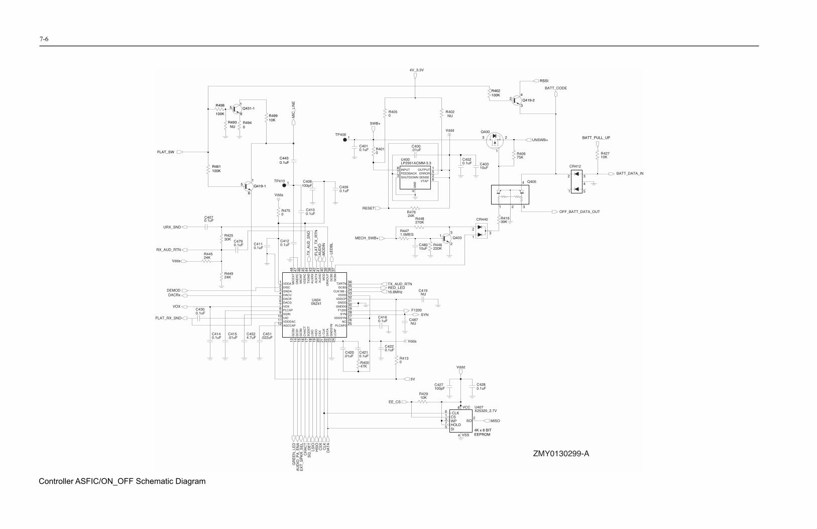
7-6
0.1uFC428
12
4
3
6
75
U407X25320_2.7V
MISO
8
WP
CLKCS
HOLDSI
SO
VCC
VSS4K x 8 BITEEPROM
100pFC427
R42910K
EE_CS
5V
R4130
47KR400
C4220.1uF
C487NU
0.1uFC421
Vdda
.01uFC420
SQ
DE
T
GN
DS
YN
HS
IO
LCA
P
LSIO
GC
B0
GC
B1
GC
B2
CLK
CS
X
DA
TA
CH
AC
T17 2319 2418151413 2120 2216
VOX
UIO
VDDA
VDDDAC
PLCAPSQIN
GNDA
DACGDACRDACU
DISC
AGCCAP
7
10
1
11
89
3
654
2
12
U40409Z41
VDDSYN
TXRTN
VDDCPVDDD
NCPLCAP2
SYN
GNDDGNDD0
F1200
GCB3CLK168
VD
DR
CT
XS
ND
UR
XO
UT
MIC
INT
MO
D
GN
DR
CM
ICE
XT
GC
B4
GC
B5
AU
DIO
AU
XR
XA
UX
TX
45 44 3946 404748 37384143 42
TX
_AU
D_S
ND
MO
DIN
AU
DIO
FLA
T_T
X_R
TN
LED
BL
270KR448
220KR446C480
10uF
R4471.5MEG
MECH_SWB+
CR440
1
23
39KR416
13
2
Q403
Q405
2
4
1 3
C4020.1uF C403
10uF
3
1
2
Q400
75KR406
UNSWB+
10KR427
5
3
1
2
4
CR412
BATT_CODE
27
36
3233
2625
28
313029
3534
C4160.1uF
SYNF1200
TX_AUD_RTN
16.8MHzRED_LED
C419NU
DA
TA
CLK
CS
X
CH
AC
TS
Q_D
ET
LSIO
HS
IO
EX
T_S
PK
R_S
EL
AU
DIO
_PA
_EN
AG
RE
EN
_LE
D
Vddd
BATT_DATA_IN
OFF_BATT_DATA_OUTR47624K
OUTPUT
SENSESHUTDOWNVTAP
ERRORFEEDBACK
GN
D
INPUT
LP2951ACMM-3.3U400
4
1
26
5378
C400.01uF
4V_3.3V
NUR402
0R405
SWB+
Vddd
MIC
_LIN
E
TP4061
C4010.1uF
0R401
0.1uFC410
TP410 1 C408100pF
0.1uFC409
0R475
Vdda
RESET
C4110.1uF
C4120.1uF
DEMOD
24KR449
C47930K
0.1uF
R425
0.1uFC407
R44524K
Vdda
URX_SND
RX_AUD_RTN
VOX
DACRx
FLAT_RX_SND
C4300.1uF
.01uFC415
4.7uFC452
0.1uFC414 C451
.022uF
FLAT_SW
R461100K
6
51
Q431-1R498
100K
R493 NU
R4940
R49910K
15
6
Q419-1
C4430.1uF
R462100K 4
3
2 Q419-2
RSSI
BATT_PULL_UP
ZMY0130299-A
Controller ASFIC/ON_OFF Schematic Diagram

7-7
PH1_PW2PH2_PW3PH3_PW4PH4_CSIOPH5_CSGP1PH6_CSGP2PH7_CSPROG
PG1_XA14PG2_XA15PG3_XA16PG4_XA17PG5_XA18PG6_AS
PH0_PW1
PG0_XA13
PC0_DATA0PC1_DATA1PC2_DATA2PC3_DATA3PC4_DATA4PC5_DATA5PC6_DATA6PC7_DATA7
VS
SR
VS
S
VS
SL
PI1
PI2
PI3
PI4
PI5
PI6
PI7
PI0
PF
2_A
DD
R2
PF
3_A
DD
R3
PF
4_A
DD
R4
PF
5_A
DD
R5
PF
6_A
DD
R6
PF
7_A
DD
R7
PF
O_A
DD
R0
PF
1_A
DD
R1
PB
1_A
DD
R9
PB
2_A
DD
R10
PB
3_A
DD
R11
PB
4_A
DD
R12
PB
5_A
DD
R13
PB
6_A
DD
R14
PB
7_A
DD
R15
PB
O_A
DD
R8
AV
SS
XIRQ
PJ1_CSGP4PJ2PJ3PJ4PJ5PJ6PJ7
RESET
PJ0_CSGP3
PG7_R_W
PE1_AN1PE2_AN2PE3_AN3PE4_AN4PE5_AN5PE6_AN6PE7_AN7
PE0_AN0
ECLKIRQ
MODA_LIRMODB_VSTBY
XF
C
XT
AL
VD
D
VD
DL
VD
DR
VD
DS
YN
VR
HV
RL
PD
0_R
XD
PD
1_T
XD
PD
2_M
ISO
PD
3_M
OS
IP
D4_
SC
KP
D5_
SS
PD
6_LV
IN
PA
0_IC
3P
A1_
IC2
PA
2_IC
1P
A3_
IC4_
OC
5_O
C1
PA
4_O
C4_
OC
1P
A5_
OC
3_O
C1
PA
6_O
C2_
OC
1P
A7_
PA
1_O
C1
AV
DD
EX
TA
L
LVO
UT
MC68HC11FL0U409
48944
8996
5857 VST
72737475767778
71 CSGP3CSGP4
66656463626160
67
8713 4055545352515049 56 7010119211587 14272625242322 2928
3031323334353637
46454443424138
47
16201917185
6
979899100
123 7980818283848586 9391 1292696890 95 3988 59
C431100pF 100pF
C449 C453100pF
C423100pF
R41110K 100pF
C456
NUC493
KEY_INT
RESETR_W
RTA0
RTA2RTA3SB1SB2PJ6OFF_BATT_DATA_OUT
RTA1
PE2VOL
RSSIVOXKEYPAD_COLKEYPAD_ROW
PTT_MICOPT_ENA
LOCKPI1
PTT
A4A3A2A1
A17A16A15A14A13A12A11A10A9A8A7A6A5
A0
D7
D0D1D2D3D4D5D6
LVZIF_SEL
LCD_SEL
BATT_PULL_UP
RAM_CSFLASH_EN
XA18BATT_DATA_IN
CLKCSX
EE_CS
PG0
390nHL410
390nHL411
R437NU
HS
IO
DA
TA
FLA
SH
_OE
SY
N
RD
Y
LSIO
SQ
_DE
TC
HA
CT
MIS
O
R4180
1
TP401TEST_POINT
SCI
F1200Vddd
R45710K
Vddd Vddd
LOW BATT
91KR415
180KR414
.01uFC433
.01uFC433
100pFC494
TP415TEST_POINT1
Vddd
Mech_SWB+
RT40033.0K
51KR432
UNSWB+ SWB+
6
4
1
3
2
3
5 1
2
4
CR413R463300
4.7K
47K
47K
10K
Q417
TEST_POINTTP405
1
BOOT_CTRL
4.7KR419
5
3
1
2
4
C4350.1uF 4.7K
R4600.1uFC434
2
1V
SS
VIN VOUT 3ILC7062CM-33U410
3.3V
UNSWB+VdddFLAT_SW
Vddd
Q418
47K47K
18K
CR414
4.7K
ZMY0130300-A
Controller Micro Processor Schematic Diagram

7-8
26 1817161514133 1931112451110 20
A11
A10
A9
A8
A7
A6
A5
A4
A3
A2
A1
A0
A14
A17
A16
A15
A13
A12
A9
A17
A2
A3
A4
A5
A6
A7
A8
A1
A10
A11
A12
A13
A14
A15
A16
A0
D7
NC D0
D1
D2
D3
D4
D5
D6
FLASH ROM
24
GND
XA
18
D0
D1
D2
D3
D4
D5
D6
D7
299 21222325262728
EN
_CE
EN
_OE
EN
_WE
VCC
FLA
SH
_EN
U406
AT
49BV
0208
303270
R492
NU
R408
XA
18
C429
0.1uF
100KR
410
FLA
SH
_OE
2.2R
428
C424
10uF
VSS
14
WE
OE
CS
27 22 20
D0
D1
D2
D3
D4
D5
D6
D7
D2
D3
D4
D5
D6
D7
D8
D1
RA
M
12131516171819 11
A4
A5
A6
A7
A8
A9
A1
A10
A11
A12
A13
A14
A2
A3
A0
VDD 28U
405S
RM
2B256
65432524 921232261 87 10A
0
A1
A2
A3
A4
A5
A6
A7
A8
A9
A10
A11
A12
A13
A14
RA
M_C
S
C425
0.1uF100pFC
426
Vddd
R478
10K
Vddd
R_W
ZM
Y0130301-O
Controller Memory Schematic Diagram

7-9
C4470.1uF
AUDIO
R46710K
3.6KR472
Vddd
10uFC476
Q433
0.1uFC450
1000pFC489
Q410
2
6 4
1 3AUDIO_PA_ENA
47KR423
TDA8547U420
OUT2NEG
8OUT2POS
6SELECT
5SVR
20
VC
C1
11
VC
C2
MODE
NC12
NC27
NC39
NC412
NC519
18OUT1NEG
3OUT1POS
13
1G
ND
1
10G
ND
2
17IN1NEG
16IN1POS
14IN2NEG
15IN2POS
4
R4715.6K
R434NU
R438
5V
Vdda
SWB+
0
2KR435
100KR496
100KR439
R436180K
Q420
C4404.7uF
C4861000pF
C4881000pF
100K
Q421
R495
PTT_MIC
Vddd
470pFC473
390nHL400
MIC
Speaker/Mic Connector
MIC_LINE
SPPSPN
10
0.1uF
R473
C442
100pFC472C471
100pF100pFC470
100pFC485
100pFC483
100pFC484
4
1
J402-33
J402-4
J402-1
J402-22
GND
INT_MIC
INT_SPN
SPP
J402
INT_SPN INT_MIC
10uFC475
UNSWB+
ZMY0130302-A
Controller Audio Power Amplifier Schematic Diagram

7-10
R481
24K
C466
100pFC
458100pF
100pFC
459
0.1uFC
467
0.1uFC
481C
4820.1uF
100pFC
463E400
UR
X_S
ND
PG
0
PI1
PJ6
PE
2
TX
_AU
D_S
ND
KE
Y_IN
T
MIS
O
RX
_AU
D_R
TN
FLA
T_R
X_S
ND
FLA
T_T
X_R
TN
OP
T_E
NA
TX
_AU
D_R
TN
DA
TA
CLK
SW
B+
KE
YP
AD
_RO
W
LCD
_SE
L
LED
BL
Vddd
RD
Y
PT
T
KE
YP
AD
_CO
L
40 417 11123031 26 6721 192039 315163435 2182538 24 10 59293637 28 82223 127 13143233
J400-4
J400-17
J400-40
J400-12
J400-30J400-31
J400-11
J400-26
J400-7
J400-21
J400-6
J400-19J400-20
J400-39
J400-3
J400-16
J400-35
J400-15
J400-18
J400-34
J400-38
J400-2
J400-24J400-25
J400-10
J400-5
J400-29
J400-37
J400-9
J400-36
J400-28
J400-8
J400-22J400-23
J400-1
J400-27
J400-14
J400-33
J400-13
J400-32
J40040-P
in Connector
ZM
Y0130303-O
Controller Interface Schematic Diagram

7-11
3.4 Controller Schematics (403-470MHz for 8480672Z04, Z06 & 136-174MHz for 8480675Z03, Z04)
INT_MIC
INT_SPN
SCI
SPNSPP
MIC
BATT_CODE
VddaRESET
4V_3.3V
GREEN_LEDRED_LED
RTA1RTA2
VOL
SB1
RTA0
RTA3
5V
CSXDACRx
DATAMODIN
SWB+LVZIF_SEL
PTT
16.8MHz
DEMOD
LOCK
MECH_SWB+
RSSI
SB2
UNSWB+
CLK
INT_MIC
INT_SPN
SCI
SPNSPP
MIC
BATT_CODE
VddaRESET
RED_LED
RTA1RTA2
VOL
SB1
RTA0
RTA3
5V
CSXDACRx
DATAMODIN
SWB+LVZIF_SELPTT
GREEN_LED
16.8MHz
DEMOD
LOCK
MECH_SWB+
RSSI
SB2
UNSWB+
CLK
4V_3.3V
IF_5V_CTRL
IF_BATT_CODE_CTRL
IF_PTT_CTRL
IF_MECHSWB+_CTRL
IF_SCI_CTRL
IF_SB1_CTRL
IF_RED_LED_CTRL
IF_DATA_CTRL
IF_CSX_CTRLIF_MODIN_CTRL
IF_16.8MHz_CTRLIF_RSSI_CTRL
IF_SB2_CTRL
IF_GREEN_LED_CTRL
IF_VOL_CTRL
IF_RTA2_CTRL
IF_DACRX_CTRL
IF_RTA3_CTRL
IF_RTA1_CTRL
IF_MIC_CTRL
IF_CLK_CTRL
IF_DEMOD_CTRL
IF_LOCK_CTRLIF_UNSWB+_CTRL
IF_LVZIF_SEL_CTRLIF_SWB+_CTRL
IF_SPP_CTRL
IF_RTA0_CTRL
IF_INT_SPN_CTRL
IF_INT_MIC_CTRL
IF_4V_3.3V_CTRL
IF_SPN_CTRL
IF_RESET_CTRLIF_Vdda_CTRL
C432
R403
VdddVdda
NU
NU
PTT
RDY
RX_AUD_RTN
SWB+
TX_AUD_RTNTX_AUD_SND
URX_SND
Vddd
CLK
DATA
FLAT_RX_SND
FLAT_TX_RTN
KEYPAD_COLKEYPAD_ROW
KEY_INT
LCD_SEL
LEDBL
MISO
OPT_ENA
PE2
PG0PI1
PJ6
ON
PG0PI1
PJ6PE2
FLAT_TX_RTN
KEY_INTPTT
LEDBL
DATAMISO
CLK
LCD_SEL
SWB+Vddd
FLAT_RX_SND
TX_AUD_SND
OPT_ENA
RX_AUD_RTN
TX_AUD_RTN
RDY
KEYPAD_ROW
URX_SND
KEYPAD_COL
Interface
D7
FLA
SH
_EN
FLA
SH
_OE
RA
M_C
S
R_W
Vdd
d
XA
18
A17
A2A3A4A5A6A7A8A9
D0D1D2D3D4D5D6
A0A1
A10A11A12A13A14A15A16
Memory
FLA
SH
_OE
RA
M_C
S
FLA
SH
_EN
R_W
Vdd
d
XA
18
RTA3
R_W
SB1
SB2
SCI
SQ
_DE
T
SW
B+
SY
N
UN
SW
B+
VOL
VO
X
Vddd
XA18
MIS
O
OFF_BATT_DATA_OUT
OPT_ENA
PE2
PG0PI1PJ6
PT
T
PTT_MIC
RAM_CS
RDYRE
SE
T
RSSI
RTA0
RTA1
RTA2
D7
DA
TA
EE
_CS
F12
00
FLASH_EN
FLASH_OE
FLAT_SW
HS
IOKEYPAD_COL
KEYPAD_ROWK
EY
_IN
T
LCD_SEL
LOC
K
LSIO
LVZIF_SEL
MECH_SWB+A6A7A8A9
BA
TT
_DA
TA
_IN
BATT_PULL_UP
CH
AC
T
CLK
CS
X
D0D1D2D3D4D5D6
A0A1
A10A11A12A13A14A15A16A17
A2A3A4A5
Micro_P
LVZIF_SEL
BATT_PULL_UP
LCD_SEL
MISO
SWB+
RESET
UNSWB+
CLK
CSX
DATA
KE
Y_I
NT
PT
T
LOC
K
PE2
PG0PI1PJ6
OPT_ENA
RDY
FLAT_SW
RTA1
RTA0
RTA2
SB1
RTA3
SB2
OFF_BATT_DATA_OUT
VOL
MECH_SWB+
KEYPAD_COL
KEYPAD_ROW
RSSI
SCI
SY
N
TX
_AU
D_R
TN
TX
_AU
D_S
ND
UN
SW
B+
UR
X_S
ND
VO
X
Vdda
Vddd
FLA
T_T
X_R
TN
GR
EE
N_L
ED
HS
IO
LED
BL
LSIO
ME
CH
_SW
B+
MIC_LINE
MIS
O
MO
DIN
OF
F_B
AT
T_D
AT
A_O
UT
RE
D_L
ED
RE
SE
T
RSSI
RX
_AU
D_R
TN
SQ
_DE
T
SW
B+
AUDIO
AUDIO_PA_ENA
BA
TT
_CO
DE
BA
TT
_DA
TA
_IN
BATT_PULL_UP
CH
AC
T
CLK
CS
X
DACRX
DA
TA
DEMOD
EE
_CS
EXT_SPKR_SEL
F12
00
FLAT_RX_SNDFLAT_SW
16.8
MH
z
4V_3.3V
5V
Vddd
FLAT_SW
BATT_PULL_UP
RSSI
BA
TT
_CO
DE
4V_3.3V
GR
EE
N_L
ED
OF
F_B
AT
T_D
AT
A_O
UT
RE
D_L
ED
TX
_AU
D_R
TN
ME
CH
_SW
B+
LED
BL
UR
X_S
ND
MO
DIN
FLA
T_T
X_R
TN
RX
_AU
D_R
TN
TX
_AU
D_S
ND
16.8
MH
z
DACRX
DEMOD ASFIC
TP
402
1
5V
Vddd
Vdd
a
FLA
T_R
X_S
ND
Vdd
a
Vdd
d
5V
AU
DIO
AU
DIO
_PA
_EN
A
INT
_MIC
INT
_SP
N
MIC
MIC
_LIN
E
PT
T_M
IC
SP
N
SP
P
SW
B+
UN
SW
B+
INT
_SP
N
INT
_MIC
MIC
SP
N
SP
P
Audio_PA
SH402SHIELD
11
SH400SHIELD
11
SH403SHIELD
SH401SHIELD
Memory Shield On/Off Shield ASFIC/Audio PA ShieldMicroprocessorShield
ZMY0130297-A
Complete Controller Schematic Diagram

7-12
0.1uFC428
12
4
3
6
75
U407X25320_2.7V
MISO
8
WP
CLKCS
HOLDSI
SO
VCC
VSS4K x 8 BITEEPROM
100pFC427
R42910K
EE_CS
5V
R4130
47KR400
C4220.1uF
C487NU
0.1uFC421
Vdda
.01uFC420
SQ
DE
T
GN
DS
YN
HS
IO
LCA
P
LSIO
GC
B0
GC
B1
GC
B2
CLK
CS
X
DA
TA
CH
AC
T17 2319 2418151413 2120 2216
VOX
UIO
VDDA
VDDDAC
PLCAPSQIN
GNDA
DACGDACRDACU
DISC
AGCCAP
7
10
1
11
89
3
654
2
12
U40409Z41
VDDSYN
TXRTN
VDDCPVDDD
NCPLCAP2
SYN
GNDDGNDD0
F1200
GCB3CLK168
VD
DR
CT
XS
ND
UR
XO
UT
MIC
INT
MO
D
GN
DR
CM
ICE
XT
GC
B4
GC
B5
AU
DIO
AU
XR
XA
UX
TX
45 44 3946 404748 37384143 42
TX
_AU
D_S
ND
MO
DIN
AU
DIO
FLA
T_T
X_R
TN
LED
BL
Q405
2
4
1 3
C4020.1uF C403
10uF
3
1
2
Q400
75KR406
UNSWB+
10KR427
BATT_CODE
27
36
3233
2625
28
313029
3534
C4160.1uF
SYNF1200
TX_AUD_RTN
16.8MHzRED_LED
C419NU
DA
TA
CLK
CS
X
CH
AC
TS
Q_D
ET
LSIO
HS
IO
EX
T_S
PK
R_S
EL
AU
DIO
_PA
_EN
AG
RE
EN
_LE
D
Vddd
BATT_DATA_IN
OFF_BATT_DATA_OUTR47624K
OUTPUT
SENSESHUTDOWNVTAP
ERRORFEEDBACK
GN
D
INPUT
LP2951ACMM-3.3U400
4
1
26
5378
C400.01uF
4V_3.3V
NUR402
0R405
SWB+
Vddd
MIC
_LIN
E
TP4061
C4010.1uF
0R401
0.1uFC410
TP410 1 C408100pF
0.1uFC409
0R475
Vdda
RESET
C4110.1uF
C4120.1uF
DEMOD
24KR449
C47930K
0.1uF
R425
0.1uFC407
R44524K
Vdda
URX_SND
RX_AUD_RTN
VOX
DACRx
FLAT_RX_SND
C4300.1uF
.01uFC415
4.7uFC452
0.1uFC414 C451
.022uF
FLAT_SW
R461100K
6
51
Q431-1R498
100K
R493 NU
R4940
R49910K
1
5
6
Q419-1
C4430.1uF
R462100K 4
3
2 Q419-2
RSSI
BATT_PULL_UP
R41610K
K1K2K3
CR412
A1A2A3
32
45
CR440
1
23
15KR451
R455NU
0R456
Q403
13
2
R44810K
R452100K
NU220KR446C480
10uF
R454NU
R447100K
MECH_SWB+
3.28V
3.28V
7.45V
0V
3.29V
ZMY0130299-D
Controller ASFIC/ON_OFF Schematic Diagram

7-13
PH1_PW2PH2_PW3PH3_PW4PH4_CSIOPH5_CSGP1PH6_CSGP2PH7_CSPROG
PG1_XA14PG2_XA15PG3_XA16PG4_XA17PG5_XA18PG6_AS
PH0_PW1
PG0_XA13
PC0_DATA0PC1_DATA1PC2_DATA2PC3_DATA3PC4_DATA4PC5_DATA5PC6_DATA6PC7_DATA7
VS
SR
VS
S
VS
SL
PI1
PI2
PI3
PI4
PI5
PI6
PI7
PI0
PF
2_A
DD
R2
PF
3_A
DD
R3
PF
4_A
DD
R4
PF
5_A
DD
R5
PF
6_A
DD
R6
PF
7_A
DD
R7
PF
O_A
DD
R0
PF
1_A
DD
R1
PB
1_A
DD
R9
PB
2_A
DD
R10
PB
3_A
DD
R11
PB
4_A
DD
R12
PB
5_A
DD
R13
PB
6_A
DD
R14
PB
7_A
DD
R15
PB
O_A
DD
R8
AV
SS
XIRQ
PJ1_CSGP4PJ2PJ3PJ4PJ5PJ6PJ7
RESET
PJ0_CSGP3
PG7_R_W
PE1_AN1PE2_AN2PE3_AN3PE4_AN4PE5_AN5PE6_AN6PE7_AN7
PE0_AN0
ECLKIRQ
MODA_LIRMODB_VSTBY
XF
C
XT
AL
VD
D
VD
DL
VD
DR
VD
DS
YN
VR
HV
RL
PD
0_R
XD
PD
1_T
XD
PD
2_M
ISO
PD
3_M
OS
IP
D4_
SC
KP
D5_
SS
PD
6_LV
IN
PA
0_IC
3P
A1_
IC2
PA
2_IC
1P
A3_
IC4_
OC
5_O
C1
PA
4_O
C4_
OC
1P
A5_
OC
3_O
C1
PA
6_O
C2_
OC
1P
A7_
PA
1_O
C1
AV
DD
EX
TA
L
LVO
UT
MC68HC11FL0U409
48944
8996
5857 VST
72737475767778
71 CSGP3CSGP4
66656463626160
67
8713 4055545352515049 56 7010119211587 14272625242322 2928
3031323334353637
46454443424138
47
16201917185
697989910
0123 7980818283848586 9391 1292696890 95 3988 59
C431100pF 100pF
C449 C453100pF
C423100pF
R41110K 100pF
C456
NUC493
KEY_INT
RESETR_W
RTA0
RTA2RTA3SB1SB2PJ6OFF_BATT_DATA_OUT
RTA1
PE2VOL
RSSIVOXKEYPAD_COLKEYPAD_ROW
PTT_MICOPT_ENA
LOCKPI1
PTT
A4A3A2A1
A17A16A15A14A13A12A11A10A9A8A7A6A5
A0
D7
D0D1D2D3D4D5D6
LVZIF_SEL
LCD_SEL
BATT_PULL_UP
RAM_CSFLASH_EN
XA18BATT_DATA_IN
CLKCSX
EE_CS
PG0
390nHL410
390nHL411
R437NU
HS
IO
DA
TA
FLA
SH
_OE
SY
N
RD
Y
LSIO
SQ
_DE
TC
HA
CT
MIS
O
R4180
1
TP401TEST_POINT
SCI
F1200Vddd
R45710K
Vddd Vddd
LOW BATT
91KR415
180KR414
.01uFC433
.01uFC433
100pFC494
TP415TEST_POINT1
Vddd
Mech_SWB+
RT40033.0K
51KR432
UNSWB+ SWB+
6
4
1
3
2
3
5 1
2
4
CR413R463300
4.7K
47K
47K
10K
Q417
TEST_POINTTP405
1
BOOT_CTRL
4.7KR419
5
3
1
2
4
C4350.1uF 4.7K
R4600.1uFC434
2
1V
SS
VIN VOUT 3ILC7062CM-33U410
3.3V
UNSWB+VdddFLAT_SW
Vddd
Q418
47K47K
18K
CR414
4.7K
3.28V
1.90V
3.30V
3.30V
ZMY0130300-B
Controller Micro Processor Schematic Diagram

7-14
26 1817161514133 1931112451110 20
A11
A10
A9
A8
A7
A6
A5
A4
A3
A2
A1
A0
A14
A17
A16
A15
A13
A12
A9
A17
A2
A3
A4
A5
A6
A7
A8
A1
A10
A11
A12
A13
A14
A15
A16
A0
D7
NC D0
D1
D2
D3
D4
D5
D6
FLASH ROM
24
GND
XA
18
D0
D1
D2
D3
D4
D5
D6
D7
299 21222325262728
EN
_CE
EN
_OE
EN
_WE
VCC
FLA
SH
_EN
U406
AT
49BV
0208
30327
2
NU
R408
XA
18
C429
0.1uF
100KR
410
FLA
SH
_OE
2.2R
428
C424
10uF
VSS
14
WE
OE
CS
27 22 20
D0
D1
D2
D3
D4
D5
D6
D7
D2
D3
D4
D5
D6
D7
D8
D1
RA
M
12131516171819 11
A4
A5
A6
A7
A8
A9
A1
A10
A11
A12
A13
A14
A2
A3
A0
VDD 28U
405S
RM
2B256
65432524 921232261 87 10A
0
A1
A2
A3
A4
A5
A6
A7
A8
A9
A10
A11
A12
A13
A14
RA
M_C
S
C425
0.1uF100pFC
426
Vddd
R478
10K
Vddd
ZM
Y0130301-O
Controller Memory Schematic Diagram

7-15
C4470.1uF
AUDIO
R46710K
36K(UHF),3.6K(VHF)R472
Vddd
10uFC476
Q433
NUC450
NUC489
Q410
2
6 4
1 3AUDIO_PA_ENA
470K(UHF),47K(VHF)R423
TDA8547U420
OUT2NEG
8OUT2POS
6SELECT
5SVR
20
VC
C1
11
VC
C2
MODE
NC12
NC27
NC39
NC412
NC519
18OUT1NEG
3OUT1POS
13
1G
ND
1
10G
ND
2
17IN1NEG
16IN1POS
14IN2NEG
15IN2POS
4
R4715.6K
R434NU
R438
5V
Vdda
SWB+
0
2KR435
100KR496
100KR439
R43647K(UHF),180K(VHF)
Q420
C4404.7uF
C486NU
C488NU
100K
Q421
R495
PTT_MIC
Vddd
470pFC473
390nHL400
MIC
Speaker/Mic Connector
MIC_LINE
SPPSPN
10
0.1uF
R473
C442
100pFC472C471
100pF100pF(UHF),NU(VHF)C470
100pFC485
100pFC483
100pFC484
4
1
J402-33
J402-4
J402-1
J402-22
GND
INT_MIC
INT_SPN
SPP
J402
INT_SPN INT_MIC
10uFC475
UNSWB+
ZMY0130302-B
Controller Audio Power Amplifier Schematic Diagram

7-16
R481
24K
C466
100pFC
458100pF
100pFC
459
0.1uFC
467
0.1uFC
481C
4820.1uF
100pFC
463E400
UR
X_S
ND
PG
0
PI1
PJ6
PE
2
TX
_AU
D_S
ND
KE
Y_IN
T
MIS
O
RX
_AU
D_R
TN
FLA
T_R
X_S
ND
FLA
T_T
X_R
TN
OP
T_E
NA
TX
_AU
D_R
TN
DA
TA
CLK
SW
B+
KE
YP
AD
_RO
W
LCD
_SE
L
LED
BL
Vddd
RD
Y
PT
T
KE
YP
AD
_CO
L
40 417 11123031 26 6721 192039 315163435 2182538 24 10 59293637 28 82223 127 13143233
J400-4
J400-17
J400-40
J400-12
J400-30J400-31
J400-11
J400-26
J400-7
J400-21
J400-6
J400-19J400-20
J400-39
J400-3
J400-16
J400-35
J400-15
J400-18
J400-34
J400-38
J400-2
J400-24J400-25
J400-10
J400-5
J400-29
J400-37
J400-9
J400-36
J400-28
J400-8
J400-22J400-23
J400-1
J400-27
J400-14
J400-33
J400-13
J400-32
J40040-P
in Connector
ZM
Y0130303-O
Controller Interface Schematic Diagram

8-1
Section 8
KEYPAD BOARD INFORMATION
1.0 Theory of Operation
KeypadU602 is a comparator that will compare the voltage when any one of the keypad row or keypad column keys is being pressed. Therefore when a key is being pressed, it will send a message to the microprocessor through the output (KEY_INT) telling it that a key has been pressed. The microprocessor will then sample the Analog to Digital voltages at the keypad row and keypad column and map it with the table so that the key being pressed can be identified.
2.0 Troubleshooting Chart
Figure 8-2 Keypad Board Troubleshooting Chart
Figure 8-1 Keypad Block Diagram
40 pin connector
Comparator
Keypad
Button9 pi
n co
nnec
tor
Key_Int
Keypad Column
Keypad
Data
Row
Tone
End
Disconnect and reconnect 40-pin
flex
No
Yes
Press Keypad

8-2 Parts List (Keypad)
3.0 Parts List (Keypad)
Circuit RefMotorola Part No.
Description
C603 2113740F51 100pFC606 2113743E20 0.1uFC607 2113740F51 100pFC609 2113740F51 100pFC610 2113740F51 100pFC611 2113740F51 100pFC612 2113928D08 10uFC613 2113740F51 100pFC614 2113740F51 100pFC615 2113740F51 100pFC616 2113740F51 100pFJ600 0985627Z01 11 pin connectorJ601 0980521Z01 44 pin connectorR618 0660076E90 51KR619 0660076E90 51KR621 0662057P15 13KR622 0660079J37 22KR623 0660079J72 43KR624 0662057G19 130K R627 0662057P15 13KR628 0660079J37 22K R629 0660079J72 43K R630 0662057G19 130K R634 0660076E90 51K R635 0662057B16 560K R636 0662057B22 1Meg U602 5102463J49 LMC7211 Com-
parator8485642Z01 PC Board

Keypad Board And Schematic Diagram 8-3
4.0 Keypad Board And Schematic Diagram
M604
M605
M608
M622
M610 M611
M613 M614
M616 M617
M619 M620
M618
M621
M612
M615
TP14
TP15
TP16
M606M623
TP7
TP8
TP9
GP88S002-A
R61
9
C60
7
19
J600
C60
3
C609C610
C611
C612
R618
R62
1
R62
2
R627
R62
8
R62
9
R63
0
R634 R63
5
R636
U60
2
R623 R624
C606
C614C615C616
C613
J6012
39
40
ZMY0130326-A
Keypad Board Top and Bottom View (PCB No. 8485642Z01)
Top View Bottom View

8-4 Keypad Board And Schematic Diagram
J601-14J601-15
J601-12J601-13
J601-31
J601-29J601-30
J601-27J601-28
J601-25J601-26
J601-23J601-24
J601-22
J601-39J601-40
J601-37J601-38
J601-35J601-36
J601-33J601-34
J601-32
J601-20J601-21
J601-18J601-19
J601-16J601-17
J601-11
J601-2
J601-10
J601-5J601-6
J601-3J601-4
J601-8J601-9
J601-1
J601-7
RDYOPT_ENA
TX_AUD_SND
FLAT_RX_SND
RX_AUD_RTN
TX_AUD_RTN
URX_SND
FLAT_TX_RTN
Vddd
SWB+
KEYPAD_ROWKEYPAD_COL
KEY_INT
PTTMISO
LEDBL
DATA
CLK
LCD_SEL
J601-44
J601-42J601-43
J601-41
J601 44-Pin Connector
J600-101011 J600-11
GND
9 J600-9J600-88
J600-33
J600-77
J600-22J600-11
4 J600-4
6 J600-6J600-55
CLK
DATA
VdddSWB+
LCD_SEL
LEDBL
J600 11-Pin Connector
Vddd
C6060.1uF
Vddd
C607100pF
C615100pF
C614100pF
C613100pF
C616100pF
KEYPAD_ROW
KEYPAD_COL
100pFC603
43KR629
13KR627
R62113K
R62822K
R62222K
51KR618
51KR619
43KR623
ROW2 ROW3 ROW4
R63451K
560KR635
4
31
2
5
U602LMC7211
1MEGR636
100pFC609
100pFC610
100pFC611
10uFC612
Vddd
KEY_INT
COL2 COL3
Vddd
COL4
130KR624
130KR630
COL5
ROW5
GND3
IN4
OUT11
OUT22
*
SWITCHM619
COL2KEYPAD_COL
GND3
IN4
OUT11
OUT22
M616SWITCH
7
GND3
IN4
OUT11
OUT22
SWITCHM613
4
GND3
4 IN
OUT11
OUT22
M610SWITCH
1
IN4
OUT11
OUT22
M604SWITCH
GND3
COL5
ROW3
PHN4
OUT11
OUT22
SWITCHM605
GND3
INTP81
ROW5ROW4
UP
OUT11
OUT22
M606SWITCH
GND3
IN4
TP71
P2
ROW2
KEYPAD_ROW
COL5
M608SWITCH
GND3
IN4
OUT11
OUT22
TP91
DOWN
TP141
3
IN4
OUT11
OUT22
SWITCHM611
GND
2
GND3
IN4
OUT11
OUT22
M614SWITCH
5
OUT11
OUT22
SWITCHM617
GND3
IN4
1
OUT22
M620SWITCH
GND3
IN4
OUT1
8
0
SWITCHM621
GND3
IN4
OUT11
OUT22
M618SWITCH
GND3
IN4
OUT11
OUT22
COL3
ROW4
ROW5
9
#
GND3
IN4
OUT11
OUT22
SWITCHM615
TP151
OUT22
M612SWITCH
GND3
IN4
OUT11
TP161ROW3
3
6
4 IN1OUT1
OUT22
2OUT2
M622SWITCH
3GND
GND3
4 IN1OUT1
SWITCHM623
ROW4
COL2
KEYPAD_ROW
MEM
P1
GP88S001-A
Keypad Board Schematic Diagram

9A-1
Section 9A
MODEL CHART AND TEST SPECIFICATIONS (403-470 MHZ)
1.0 Model Chart
GP88s , UHF, 403-470 MHzModel Description
AZH34RDC9AA3 GP88s 403-470 MHz 4W 16 CH
Item Description
X PMUE1542* GP88s Super Tanapa 403-470 MHz 4W
X PMUE1543* GP88s Tanapa 403-470 MHz 4W
X PMLE4173 GP88s B/C Kit 403-470 MHz 4W
X PMLN4343 GP88s Front Housing Kit
X PMAE4002A Antenna, 403-433 MHz Stubby
X PMAE4003A Antenna, 430-470 MHz Helical
X NAE6483AR Antenna, 403-470 MHz Whip
X 6804111J46 GP88s User Guide
x = Indicates one of each is required.* Motorola Depot Servicing only

9A-2 Specifications
2.0 Specifications
General
Transmitter
Receiver
All specifications are subject to change without notice.
UHF
Frequency: 403-470 MHz
Channel Capacity: GP88s : 16 Channels
Power Supply: 7.5 Volts ±20%
Dimensions with Standard High Capacity NiMH Battery:
57.5mm x 134mm x 38mm
Weight: with Standard High Capacity NiMH Battery: with High Capaci-ty NiCd Battery:
429 g
454 g
Average Battery Life @ (5-5-90 Duty Cycle) Standard High Capacity NiMH Bat-tery:
Low Pow-er
10 hrs
High Pow-er
8 hrs
Sealing: Passes rain testing per IP54
Shock: Meets MIL-STD-810-C,D & E and TIA/EIA 603
Vibration: Meets MIL-STD-810-C,D & E and TIA/EIA 603
Dust: Meets MIL-STD-810-C,D & E and IP54
Humidity: Meets MIL-STD-810-C,D & E and TIA/EIA 603
UHF
RF OutputNiMH @ 7.5V:
Low1W
High4W
Frequency 403-470 MHz
Channel Spacing 12.5/20/25 kHz
Freq. Stability(-30°C to +60°C)
0.00025%
Spurs/Harmonics: -36 dBm < 1 GHz-30 dBm > 1 GHz
Audio Response:(from 6 dB/oct. Pre-Emphasis, 300 to 3000Hz)
+1, -3 dB
Audio Distortion:@ 1000 Hz, 60%Rated Max. Dev.
<5%
FM Noise: -40 dB
UHF 12.5kHz
UHF 20/25kHz
Frequency: 403-470MHz
403-470MHz
Sensitivity12dB EIA SINAD:
0.35 µV 0.35 µV
Adjacent Channel Selectivity ETS
-60 dB -70 dB
Intermodulation ETS
-65 dB -65 dB
Freq. Stability(-30°C to +60°C):
0.00025% 0.00025%
Spur Rejection: -70 dB -70 dB
Image Rejection: -70 dB -70 dB
Audio Output@ <5% Distortion
500 mW 500 mW

Transmitter 9A-3
3.0 Transmitter
3.1 General(Refer to Figure 9-1)
The UHF transmitter contains five basic circuits:
1. power amplifier
2. antenna switch
3. harmonic filter
4. antenna matching network
5. power control integrated circuit (PCIC).
3.1.1 Power Amplifier
The power amplifier consists of two devices:
1. 9Z67 LDMOS driver IC (U101) and
2. PRF1507 LDMOS PA (Q110).
The 9Z67 LDMOS driver IC contains a 2 stage amplification with a supply voltage of 7.3V.
This RF power amplifier is capable of supplying an output power of 0.3W (pin 6 and 7) with an input signal of 2mW (3dBm) (pin16). The current drain would typically be 160mA while operating in the frequency range of 403-470MHz.
The PRF1507 LDMOS PA is capable of supplying an output power of 7W with an input signal of 0.3W. The current drain would typically be 1300mA while operating in the frequency range of 403-470MHz. The power output can be varied by changing the biasing voltage.
Figure 9-1 Transmitter Block Diagram
PCIC
Antenna
PA Antenna Switch/
Driver Harmonic Filter/
Vcontrol Vcontrol
From VCO
Jack
PA-FinalStage
Matching Network

9A-4 Transmitter
3.1.2 Antenna Switch
The antenna switch circuit consists of two PIN diodes (CR101 and CR102), a pi network (C107, L104 and C106). In the transmit mode, B+ at PCIC (U102) pin 23 will go low and turn on Q111 where a B+ bias is applied to the antenna switch circuit to bias the diodes "on". The shunt diode (CR102) shorts out the receiver port, and the pi network, which operates as a quarter wave transmission line, transforms the low impedance of the shunt diode to a high impedance at the input of the harmonic filter. In the receive mode, the diodes are both off, and hence, there exists a low attenuation path between the antenna and receiver ports.
3.1.3 Harmonic Filter
The harmonic filter consists of C104, L102, C143, C103, L101, C142 and C102. The design of the harmonic filter for UHF is that of a modified Zolotarev design. It has been optimized for efficiency of the power module. This type of filter has the advantage that it can give a greater attenuation in the stop-band for a given ripple level. The harmonic filter insertion loss is typically less than 1.2dB.
3.1.4 Antenna Matching Network
A matching network which is made up of L116 and C141 is used to match the antenna's impedance to the harmonic filter. This will optimize the performance of the transmitter and receiver into an antenna.
3.1.5 Power Control Integrated Circuit (PCIC)
The transmitter uses the Power Control IC (PCIC), U102 to regulate the power output of the radio. The current to the final stage of the power module is supplied through R102 (0.075 ohm), which provides a voltage proportional to the current drain. This voltage is then fedback to the Automatic Level Control (ALC) within the PCIC to regulate the output power of the transmitter.
The PCIC has internal digital to analog converters (DACs) which provide the reference voltage of the control loop. The reference voltage level is programmable through the SPI line of the PCIC.
There are resistors and integrators within the PCIC, and external capacitors (C133, C134 and C135) in controlling the transmitter rising and falling time. These are necessary in reducing the power splatter into adjacent channels.
CR105 and its associated components are part of the temperature cut back circuitry. It senses the printed circuit board temperature around the transmitter circuits and output a DC voltage to the PCIC. If the DC voltage produced exceeds the set threshold in the PCIC, the transmitter output power will be reduced so as to reduce the transmitter temperature.

Receiver 9A-5
4.0 Receiver
4.1 Receiver Front-End(Refer to UHF Receiver Front End Schematic Diagram on page 9A-16 and UHF Harmonic Filter Schematic Diagram on page 9A-21)
The RF signal is received by the antenna and applied to a low-pass filter. For UHF, the filter consists of L101, L102, C102, C103, C104. The filtered RF signal is passed through the antenna switch. The antenna switch circuit consists of two PIN diodes(CR101 and CR102) and a pi network (C106, L104 and C107).The signal is then applied to a varactor tuned bandpass filter. The UHF bandpass filter comprises of L301, L302, C302, C303, C304, CR301 and CR302. The bandpass filter is tuned by applying a control voltage to the varactor diodes(CR301 and CR302) in the filter.
The bandpass filter is electronically tuned by the DACRx from U404 which is controlled by the microprocessor. Depending on the carrier frequency, the DACRx will supply the tuned voltage to the varactor diodes in the filter. Wideband operation of the filter is achieved by shifting the bandpass filter across the band.
The output of the bandpass filter is coupled to the RF amplifier transistor Q301 via C307. After being amplified by the RF amplifier, the RF signal is further filtered by a second varactor tuned bandpass filter, consisting of L306, L307, C313, C317, CR304 and CR305.
Both the pre and post-RF amplifier varactor tuned filters have similar responses. The 3 dB bandwidth of the filter is about 50 MHz. This enables the filters to be electronically controlled by using a single control voltage which is DACRx .
Figure 9-2 UHF Receiver Block Diagram
Demodulator
Synthesizer
Crystal Filter
MixerVaractor Tuned Filter
RF AmpVaractor Tuned Filter
Pin Diode Antenna SwitchRF Jack
Antenna
AGC
Control Voltagefrom ASFIC
First LOfrom FGU
Recovered AudioSquelch
RSSI
IF IC
SPI Bus
16.8 MHzReference Clock
SecondLO VCO
U301
IF Amp

9A-6 Receiver
The output of the post-RF amplifier filter which is connected to the passive double balanced mixer consists of T301, T302 and CR306. Matching of the filter to the mixer is provided by C381. After mixing with the first LO signal from the voltage controlled oscillator (VCO) using low side injection, the RF signal is down-converted to the 45.1 MHz IF signal.
The IF signal coming out of the mixer is transfered to the crystal filter (FL301) through a resistor pad and a diplexer (C322 and L310). Matching to the input of the crystal filter is provided by C324 and L311. The crystal filter provides the necessary selectivity and intermodulation protection.
4.2 Receiver Back-End(Refer to UHF Receiver Back End Schematic Diagram on page 9A-17)
The output of crystal filter FL301 is matched to the input of IF amplifier transistor Q302 by components R352 and C325. Voltage supply to the IF amplifier is taken from the receive 5 volts (R5). The IF amplifer provides a gain of about 7dB. The amplified IF signal is then coupled into U301(pin 3) via C330, C338 and L330 which provides the matching for the IF amplifier and U301.
The IF signal applied to pin 3 of U301 is amplified, down-converted, filtered, and demodulated, to produce the recovered audio at pin 27 of U301. This IF IC is electronically programmable, and the amount of filtering (which is dependent on the radio channel spacing) is controlled by the microprocessor. Additional filtering, once externally provided by the conventional ceramic filters, is replaced by internal filters in the IF module (U301).
The IF IC uses a type of direct conversion process, whereby the externally generated second LO frequency is divided by two in U301 so that it is very close to the first IF frequency. The IF IC (U301) synthesizes the second LO and phase-locks the VCO to track the first IF frequency. The second LO is designed to oscillate at twice the first IF frequency because of the divide-by-two function in the IF IC.
In the absence of an IF signal, the VCO will “search” for a frequency, or its frequency will vary close to twice the IF frequency. When an IF signal is received, the VCO will lock onto the IF signal. The second LO/VCO is a Colpitts oscillator built around transistor Q320. The VCO has a varactor diode, CR310, to adjust the VCO frequency. The control signal for the varactor is derived from a loop filter consisting of C362, C363, C364, R320 and R321.
The IF IC (U301) also performs several other functions. It provides a received signal-strength indicator (RSSI) and a squelch output. The RSSI is a dc voltage monitored by the microprocessor, and used as a peak indicator during the bench tuning of the receiver front-end varactor filter. The RSSI voltage is also used to control the automatic gain control (AGC) circuit at the front-end.
The demodulated signal on pin 27 of U301 is also used for squelch control. The signal is routed to U404 (ASFIC) where squelch signal shaping and detection takes place. The demodulated audio signal is also routed to U404 for processing before going to the audio amplifier for amplification.

Receiver 9A-7
4.3 Automatic Gain Control Circuit(Refer to UHF Receiver Front End Schematic Diagram on page 9A-16)
The front end automatic gain control circuit is to provide automatic gain reduction of the front end RF amplifier via feedback. This action is necessary to prevent overloading of backend circuits. This is achieved by drawing some of the output power from the RF amplifier’s output. At high radio frequencies, capacitor C331 provides the low impedance path to ground for this purpose. CR308 is a PIN diode used for switching the path on or off. A certain amount of forward biasing current is needed to turn the PIN diode on. Transistors Q315 provides this current where upon saturation, current will flow via R347, PIN diode, collector and emitter of Q315 and R319 before going to ground. Q315 is an NPN transistor used for switching here. Maximum current flowing through the PIN is mainly limited by the resistor R319.
Radio signal strength indicator, RSSI, a voltage signal, is used to drive Q315 to saturation hence turning it on. RSSI is produced by U301 and is proportional to the gain of the RF amplifier and the input RF signal power to the radio.
Resistor network at the input to the base of Q315 is scaled to turn on Q315, hence activating the AGC, at certain RSSI levels. In order to turn on Q315, the voltage across the transistor’s base to ground must be greater or equal to the voltage across R319, plus the base-emitter voltage (Vbe) present at Q315. The resistor network with thermistor RT300 is capable of providing temperature compensation to the AGC circuit, as RSSI generated by U301 is lower at cold temperatures compared to normal operation at room temperature. Resistor R300 and capacitor C397 form an R-C network used to dampen any transient instability while the AGC is turning on.

9A-8 Frequency Generation Circuitry
5.0 Frequency Generation Circuitry
The Frequency Generation Circuitry is composed of two main ICs, the Fractional-N synthesizer (U201), and the VCO/Buffer IC (U241). Designed in conjunction to maximize compatibility, the two ICs provide many of the functions that normally would require additional circuitry. The synthesizer block diagram illustrates the interconnect and support circuitry used in the region. Refer to the relevant schematics for the reference designators.
The synthesizer is powered by regulated 5V and 3.3V which come from U247 and U248 respectively. The synthesizer in turn generates a superfiltered 4.5V which powers U241.
In addition to the VCO, the synthesizer must interface with the logic and ASFIC circuitry. Programming for the synthesizer is accomplished through the data , clock and chip select lines from the microprocessor. A 3.3V dc signal from synthesizer lock detect line indicates to the microprocessor that the synthesizer is locked.
Transmit modulation from the ASFIC is supplied to pin10 of U201. Internally the audio is digitized by the Fractional-N and applied to the loop divider to provide the low-port modulation. The audio runs through an internal attenuator for modulation balancing purposes before going out to the VCO.
Figure 9-3 Frequency Generation Unit Block Diagram
Voltage Multiplier
Synthesizer U201
Dual Tran-sistor
Loop Filter
VCOBIC U241
Low Pass Filter
Matching Network
Attenuator
ToMixer
ToPA Driver
VCP
Vmult1Aux3
Aux4
MOD Out
ModulatingSignal
Vmult2
Rx VCO Circuit
Tx VCO Circuit
TRB
16.8 MHzRef. Osc.
Rx Out
Tx Out

Frequency Generation Circuitry 9A-9
5.1 Synthesizer(Refer to UHF Synthesizer Schematic Diagram on page 9A-18)
The Fractional-N Synthesizer uses a 16.8MHz crystal (FL201) to provide a reference for the system. The LVFractN IC (U201) further divides this to 2.1MHz, 2.225MHz, and 2.4MHz as reference frequencies. Together with C206, C207, C208, R204 and CR203 , they build up the reference oscillator which is capable of 2.5ppm stability over temperatures of -30 to 85°C. It also provides 16.8MHz at pin 19 of U201 to be used by ASFIC and LVZIF.
The loop filter which consist of C231, C232, C233, R231, R232 and R233 provides the necessary dc steering voltage for the VCO and determines the amount of noise and spur passing through .
In achieving fast locking for the synthesizer, an internal adapt charge pump provides higher current at pin 45 of U201 to put synthesizer within the lock range. The required frequency is then locked by normal mode charge pump at pin 43 .
Both the normal and adapt charge pumps get their supply from the capacitive voltage multiplier which is made up of C258, C259, C228, triple diode CR201 and level shifters U210 and U211. Two 3.3V square waves ( 180 deg out of phase) are first shifted to 5V, then along with regulated 5V , put through arrays of diodes and capacitors to build up 13.3V at pin 47 of U201.
Figure 9-4 Synthesizer Block Diagram
DATA
CLK
CEX
MODIN
VCC, DC5V
XTAL1
XTAL2
WARP
PREIN
VCP
REFERENCEOSCILLATOR
VOLTAGEMULTIPLIER
VOLTAGECONTROLLED OSCILLATOR
2-POLELOOPFILTER
DATA (U409 PIN 100)
CLOCK (U409 PIN 1)
CSX (U409 PIN 2)
MOD IN (U404 PIN 40)
+5V (U247 PIN 4)
7
8
9
10
13, 30
23
24
25
32
47
VMULT2 VMULT1
BIAS1
SFOUT
AUX3
AUX4
IADAPTIOUT
GND
FREFOUT
LOCK 4
19
6, 22, 23, 24
4345
3
2
28
14 15
40
FILTERED 5V
STEERINGLINE
LOCK (U409 PIN 56)
PRESCALER IN
LO RF INJECTION
TX RF INJECTION(1ST STAGE OF PA)
FREF (U201 PIN 21 & U404 PIN 34)
39BIAS2
41
DUAL TRANSIS
DUAL TRANSIS-
48
5VR5
5, 20, 34, 36(U248 PIN 5)
AUX1
VDD, 3.3V MODOUT
U251 LOW VOLTAGE FRACTIONAL-N SYNTHESIZER
TORS
TORS

9A-10 Frequency Generation Circuitry
5.2 VCO - Voltage Controlled Oscillator(Refer to UHF Voltage Controlled Oscillator Schematic Diagram on page 9A-19)
Figure 9-5 VCO Block Diagram
The VCOBIC (U241) in conjunction with the Fractional-N synthesizer (U201) generates RF in both the receive and the transmit modes of operation. The TRB line (U241 pin 19) determines which oscillator and buffer will be enabled. A sample of the RF signal from the enabled oscillator is routed from U241 pin 12, through a low pass filter, to the prescaler input (U201 pin 32). After frequency comparison in the synthesizer, a resultant CONTROL VOLTAGE is received at the VCO. This voltage is a DC voltage between 3.5V and 9.5V when the PLL is locked on frequency.
Presc
RX
TX
MatchingNetwork
Low Pass Filter
Attenuator
Pin8
Pin14
Pin10
Level Shifter Network
5V
(U201 Pin28)
VCC Buffers
TX RF Injection
U201 Pin 32
AUX4 (U201 Pin3)
AUX3 (U201 Pin2)
Prescaler Out
Pin 12Pin 19Pin 20
TX/RX/BSSwitching Network
U241VCOBIC
RxActive Bias
TxActive Bias
Pin2
Rx-I adjust
Pin1
Tx-I adjust
Pins 9,11,17Pin18
VsensCircuit
Pin15
Pin16
RX VCO Circuit
TX VCO Circuit
RX Tank
TX Tank
Pin7
Vcc-Superfilter
Collector/RF in
Pin4
Pin5
Pin6
RX
TX
(U201 Pin28)
Rx-SW
Tx-SW
Vcc-Logic
(U201 Pin28)
Steer Line Voltage (VCTRL)
Pin13
Pin3
TRB_IN
LO RF INJECTION
VSF
VSF
VSF

Frequency Generation Circuitry 9A-11
The VCOBIC(U241) is operated at 4.54 V (VSF) and Fractional-N synthesizer (U201) at 3.3V. This difference in operating voltage requires a level shifter consisting of Q260 and Q261 on the TRB line.
The operation logic is shown in Table 9-1.
In the receive mode, U241 pin 19 is low or grounded. This activates the receive VCO by enabling the receive oscillator and the receive buffer of U241. The RF signal at U241 pin 8 is run through a matching network. The resulting RF signal is the LO RF INJECTION and it is applied to the mixer at T302 (refer to UHF Receiver Front End Schematic Diagram on page 9A-16).
During the transmit condition, when PTT is depressed, five volts is applied to U241 pin 19. This activates the transmit VCO by enabling the transmit oscillator and the transmit buffer of U241. The RF signal at U241 pin 10 is injected into the input of the PA module (U101 pin16). This RF signal is the TX RF INJECTION. Also in transmit mode, the audio signal to be frequency modulated onto the carrier is received through the U201 pin 41.
When a high impedance is applied to U241 pin 19, the VCO is operating in BATTERY SAVER mode. In this case, both the receive and transmit oscillators as well as the receive transmit and prescaler buffer are turned off.
Table 9-1 Level Shifter Logic
Desired Mode
AUX 4 AUX 3 TRB
Tx Low High (@3.2V) High (@4.8V)
Rx High Low Low
Battery Saver Low Low Hi-Z/Float (@2.5V)

9A-12 Notes For All Schematics and Circuit Boards
6.0 Notes For All Schematics and Circuit Boards* Component is frequency sensitive. Refer to the Electrical Parts List for value and usage.
1. Unless otherwise stated, resistances are in Ohms (k = 1000), and capacitances are in picofarads (pF) or microfarads (µF).
2. DC voltages are measured from point indicated to chassis ground using a Motorola DC multime-ter or equivalent. Transmitter measurements should be made with a 1.2 µH choke in series with the voltage probe to prevent circuit loading.
3. Reference Designators are assigned in the following manner:
100 Series = Transmitter
200 Series = Frequency Generation
300 Series = Receiver
400/500 Series = Controller
600 Series = Keypad Board
4. Interconnect Tie Point Legend:
UNSWB+ = Unswitch Battery Voltage (7.5V)
SWB+ = Switch Battery Voltage (7.5V)
R5 = Receiver Five Volts
CLK = Clock
Vdda = Regulated 3.3 Volts (for analog)
Vddd = Regulated 3.3 Volts (for digital)
CSX = Chip Select Line (not for LVZIF)
SYN = Synthesizer
DACRX = Digital to Analog Voltage (For Receiver Front End Filter)
VSF = Voltage Super Filtered (5 volts)
VR = Voltage Regulator
6-LAYER CIRCUIT BOARD DETAIL VIEWINGCOPPER STEPS IN PROPER LAYER SEQUENCE
LAYER 1 (L1)
LAYER 2 (L2)LAYER 3 (L3)
LAYER 4 (L4)
LAYER 5 (L5)LAYER 6 (L6)
INNER LAYERS
SIDE 1
SIDE 2

Circuit Board/Schematic Diagrams and Parts List
9A
-13
7.0 Circuit Board/Schematic Diagrams and Parts List
1
J400
40
TP401
Q431
R49
3 R49
4
R49
8
R49
9
RT400
TP402TP410
C47
0
C471
C472
C483C484
C48
5
CR
413
2
1
3
4
6
5
J402
4 3
Q41
7Q
433
TP405TP406 TP415
C40
0
C40
1
C402
C403
C467
CR412
CR
440
Q40
0
43
Q405
R401
R40
2
R40
3
R405
R40
6
R41
6
R427
R476
R481
SH401
4
5 8U400
C48
0
C48
2
Q403
R44
6R
447
R44
8
C42
3 R410
R41
8
R437
22
218
71
U405
32 17
U406
C424
C425C426
C427C428
C429
R408
R428
R42
9
R478
R49
2
SH400
161
145
8
U40
7
C43
2
3
FL201
TP201
C52
3C
524
C52
5
C52
6 4 3
Q50
6V
R43
1
VR
450
VR
451
C44
6
C45
5C
515
C527
C528
R51
0
C220
C23
5
C260
C29
1 C29
4
L201
L202
L203
U247
C21
0
C211
C21
2
C213
C21
4
C21
7
C22
8
C22
9
C23
0
C25
6
C257
C292
C29
7
C29
9
CR
201
43
Q210
4 3
Q26
0
C203
C23
3
C238
L232
R255
R256
C247 C248
C27
1
C273
C28
5C
286 L282
Q241
R24
3
R248
R25
3
C27
6
1
3
L243
L271
L273
C27
2C
370
C37
4
C38
6
L321
R33
3
R33
9
SH241
C251
C253
C28
9
1
3
L2534 3
Q26
1
R26
0
C11
8
C12
0
C121
C127
C160
L115
L160
R10
5
R10
7
R108
1
16
8
9
U101
C12
2
C12
5
C12
9
C161 C16
5
C16
9
L113 L114
R16
1
C11
0
C112
C11
3
C11
4
C131C166 L106
L107
SH101
C115
C116
C117
C119
C171
L108
R103
R10
4R10
6
R12
0
R17
1
R1731
2
3
Q110
C109
C111
C32
2
C38
1
L310
R308R30
9 R310
SH303
643
T30
1
C31
9
C32
0
C37
5
L309
R348
64 3
T30
2
TP202
TP302
C32
3
C32
4
L311
C325FL3
01 R35
1
R352
SH323
PB504
VR
444
C328
C39
1
C397
R300
R314
R31
6
R325
R32
6
R33
4
R335
R338
RT301
VR
300
Q315
Q316
R318
R31
9
R32
7
RT
300
C33
1
C333
C396
CR
308
R317
R336
R34
2
C10
8
43
Q111
R10
1R
170
VR432
C498
C519
VR
433
43
2
J404
C454
C49
9C
518
C520
C301 C30
2C
303
C30
8
CR301
L301
R301
R302
SH301
C304
C30
5CR302
L302
C350
C353
C35
4
C384
C385L325
Q320
R32
4
R34
5
R34
6
SH321
C349
C351C352
C362 C363
C36
4
R32
0
R321
R32
2
R355
CR
310
L332
C50
2
C52
1
PB501PB502
VR440
VR501
C50
5
C50
6C
507
Q505
R50
5
R50
6
R50
7
C513
4 3
2CR503 Q502R
501
R50
2
C512
C140
C141
C51
1 C51
4L1
16
C477
C47
8 C50
1C
504
C50
8
C509
4
2
J407
SH201
ZMY0130320-A
UHF (403-470MHz) Main Board Top Side PCB No. 8480672Z01

9A
-14 Circuit Board/Schematic Diagrams and Parts List
4
53
2S502
4
C
8
C
2
1
S501
J104
2
3
4
1
J101
C101C102
C10
4
C14
2
CR101L101
L105
SH100
C103
C106
C107C143
C14
4
CR
102
L102
L104
E101
R329
C105
C172
C173
CR105
R102
R130
R131
R172
H101
C132
R133
C123
C126
C128
C130
C138
C150C151C152
C170
L112
C133
C13
4C
135
C17
4
R109
R132
R13
4
1
17 9
25
U102
C503
CR306
F501SH304
C30
7
C309C310
CR
303
L303
L304Q
301
R303
R304
R328
R34
0
C306
C311
C312
C313
C314
C315
C321
C395
CR304
L305
L306
L340
R30
5R
347
SH302
C316
C317C318
C380 CR305
L307
R30
6 R307
C329 C336
C337
C35
5
C360
C361
L314
C34
7
C34
8C356
SH322
C33
9
C34
0
C34
1
C34
2
C343
C346
C357C358
C359
C383
C390 R344
C33
4
C345
137
25 13
U301
C344
C38
2
L331
R34
3
R350
1
2
3
B501
C326
C327
C330C338
L330
Q30
2
R311R312
R31
3
R31
5
C277
C278
C27
9
C28
0
U24
8
C50
0
C522
CR501
L505
VR
439
VR441VR506
C201
C224
C23
1
C232
C234
R201
R202
R23
1
R23
2
R23
3
C20
2 C204
C219
C223
C263
C264
C29
3
C298L261
SH202
1
37 25
13
U201
C20
6
C207
C208
C21
8
C265
CR203
R204
R28
1
4
3
U210
C258C259
C29643
U211
C252C254
C255
CR
251
L251
R25
1
R25
2
R254
11
1 20
10
U241
C28
1
C371C372
C373
L281
Q310
R24
5
R330R331
R332
R349
C295
C378
CR241
L242
R11
0
R11
1R11
2
C241C242
C243
C244
C245
C246C250CR242
CR243
L241
R241 R242
R244
SH242
C409
C410C412
C407
C408
C411
C414
C41
5
C416
C41
9
C420C421
C42
2
C430
C442
C443
C447
C450C451
C45
2
C475
C476
C479
C481C487
43
Q410
R400R413
R423
R42
5
R445
R449
R471
R472R473
R475
SH403
1
37 25
13
U404
11
1
20
10
U420
C458
C459
C466C473
R435
C440
L400
Q42
0
Q421
R434
R43
6
R43
8
R439
R467
R495
R496
76
51
U409
R419
R462
Q41
9
R461
C431C433
C435
C494
CR414
43
Q418
R414R415
R460
R463
C489
SH402
C45
6
C49
3 R411 R457
C45
3R
432
C434
U41
0
C44
9C
463
1E400
L410
L411
C48
6
C48
8
26
ZMY0130319-A
UHF (403-470MHz) Main Board Bottom Side PCB No. 8480672Z01

Circuit Board/Schematic Diagrams and Parts List
9A
-15
10.0VVR450
10.0VVR451
0.47uFC502
MECH_SWB+
TAB1
TAB2
5
3
HIG
H
6
7
2
SWITCH
4
1LO
W
S502
0R507
Vdda
VOL
6.8VVR501 C505
100pF100pF
51
6
IMX1
24
3
SWB+
RED_LED
Q502R50510K
Q505 47KR506
Vdda
180R502
2 4
1 3CR503
R501680 RTA3
RTA2
RTA0RTA1
GREEN_LED
C514100pF100pF
C513100pF
C512100pFC511 7
GND GND19
1PC0
2PC1
4 PC2 PC38
S501SWITCH
C0 C0C1C1
CR501
24VF501
21
10VVR439
UNSWB+
1000pFC500
100pFC503
BATT_CODE
6.8VVR506
L505390nH
B501
RSSI_FIL2
NEG1
POS3
.01uFC521
2
6.8VVR440
SB1 1SWITCHPB501
6.8VVR444
2PTT
1
SWITCHPB504
.01uFC522
VR4416.8V
PB502
12SWITCH
SB2
1S1
4S2
2S3
J407
SPN
SPP
ANT_BIAS
MIC
5V
0.1uFC515
Q503
2
6
4
1
3
4.7K47K
47K
10K
10KR510
C478100pF
100pFC477
VR4316.8V
SCI
100pFC498
100pFC499
4700pFC446
C454100pF C455
470pFC5201000pF
C5181000pF
C5191000pF
C5041000pF
C5011000pF
1S1
S23
4S3
2S4
J404
INT_MIC
INT_SPN
3
1
VR43310V22
3
1
10VVR432
C5071000pF
C506100pF
C5241000pF
C523100pF
C5091000pF
C508100pF
ZMY0130312-A
UHF Controls And Switches Schematic Diagram
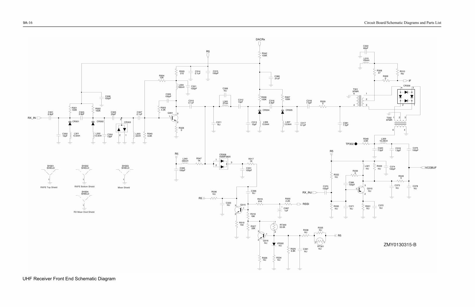
9A
-16 Circuit Board/Schematic Diagrams and Parts List
100pFC386
Q3101
3
2NU
R331 C372R330 C371NU NU NU NU
2 1
R335
RT301
R338
C3916.8KR325
R5
NU
NUNU
NU
VR300
R326
Q316
13
2
R334
NU
NUNU
NU
33.0KRT300
2
1
13
2
Q315
R319150
R31818K
R32733K
C333
R336
R5
NU
NU
R31691K
C396NU
C3971uF
2.2KR300
RSSI
RX_INJ
100pFC370
0R339
R332NU
100pFC374R333
0R349
L321
C373
NU NU
NUC378NU
100pFC375
16.28nHL309
C320 C3197.5pF 1.8pF
2T302XFMR
46
31
C3817.5pF
TP3023.6KR348
R5
7.5pFC318
9.1pFC317
R3290
CR305CR304
100KR307R306
100K
L30613.9nH
L30713.9nH
C3163.9pF
C31310pF
C311
27nHL305 13pF
C312
C306
NU
NU
R3034.3K
C3100.1uF
Q301
13
2
R3406.8K
0R328
C3140.1uF510
12K
R305
C309100pF
R304
180nHL304
100pFC321
100pFC315
R5R342100K
C380.01uF
DACRx
2
XFMRT301
4
6
3
1
0R309
NU47R310R308
CR30634
IF
2 1
82pFC322
L310150nH
R3171K
23
CR308HSMP3820
1
100pFC331C395
100pF
L340390nH
R3471K
R5
C3016.8pF
RX_INCR301
13.9nHL301C302
10pF
CR302
R302100K
R301100K
3.9pFC303
100pFC308
C30520pF
L30213.9nH
C30413pF
CR303
2
3
1 22nHL303
C3070.1uF
SHIELDSH301
1
RXFE Top Shield
SH302
1
SHIELD
1
SH304SHIELD
RXFE Bottom Shield
RX Mixer Diod Shield
SH303SHIELD
1
Mixer Shield
VCOBUF
ZMY0130315-B
UHF Receiver Front End Schematic Diagram

Circuit Board/Schematic Diagrams and Parts List
9A
-17
Vdd_FILTERED
(SOURCE)
L3312.2uH
R34310
10uFC382
C3290.1uF
0.1uFC348
0.1uFC344
Vdda
C3430.22uF
0.1uFC347 C346
0.1uF 0.1uFC345
DEMOD
100KR350
C390100pF
R34412K
100pFC383
Vdd_FILTERED
C349.022uF
C350330pF
C35120pF
.022uFC334
16.8MHz
CLKDATA
LVZIF_SEL
0.22uFC357
1200pFC358
C3590.1uF
VA
G
VA
G_R
EF
RO
SE
_VC
CR
OS
E_V
SS
LIM
PH
AS
E_L
OC
KD
EM
OD
_OU
T
C4M
DE
MO
D_H
F
C1M
C2M
C3M
TESTAIOUT
MLPD_CR
FREFGND
GOLD_VSS
CEXCLK
COL
DATA
BROWN_VCCBRP_OFF
PRE_AGC
GREEN_VSSMIX_BYP
MIX_INPREAMP_OUT
GREEN_VCC
C3PC4P
BLUE_VSS
C1PC2P
BLUE_VCC
TE
ST
DV
PP
PR
E_I
N
RE
D_V
CC
RE
D_V
SS
RS
SI_
FLT
RS
SI_
OU
T
EM
IT
EX
TB
S
GO
LD_V
CC
AF
C
BA
SE
U30132D83
8 931 2 54 116 107 12
1615
24
2120
14
1918
13
17
2223
48
4342
4647
41
3837
44
4039
45
32 2530 2931 262736 28333435
0.33uF
15pFC338
C361.01uF
RSSI
C3280.1uF
R3143K
R5
330R313
C355
C337100pF
.022uFC356
C326.01uF
L3142.2uH
C3360.1uF
Vdd_FILTERED
C3421uF
C3411uF
C3401uF
1uFC339
LVZIF BTM SHEILDCRYSTAL FILTER SHIELD LVZIF TOP SHEILD
SH322SHIELD
SH321SHIELD
SH323SHIELD
111
BFQ67WQ320
3
212pFC352
1
C35343pF
0R355
R3201K
2.2uHL325
R34656K
47pFC354
2KR324
CR310
C38556pF 100nH
L332
2.4KR321 R322
200K.01uFC364C362
.022uF
C3632.2uF
C38456pF10K
R345
C360.022uF
680nHL330
C33010pF
C327100pF
5.6KR312 Q302R351
0
R31512K
.01uFC325
30KR311
3.3KR352
XTALFL301
TBD
OUTIN
GN
DG
ND
1G
ND
2G
ND
3
36
1 2 4 5
IF
C323150pF
L311750nH
20pFC324
DB
DA
ZMY0130314-O
UHF Receiver Back End Schematic Diagram

9A
-18 Circuit Board/Schematic Diagrams and Parts List
GND3
2
NC
1 4
U210TC7SET04FU
VCC5
GND3
2
NC
1 4
VCC5
U211TC7SET04FUC296
0.1uF
C265NU 100pF
C257
A2A3
K1K2K3
A1
CR201
54
6123
C230100pF 1000pF
C2294.7uFC228
C2190.22uF
0.1uFC292
C2980.1uF
L2022.2uH
(SOURCE)5V
0.47uFC291
0.1uFC223
2.2uFC235
246
53
1
U247ADP3300
GN
D
INSD
NROUTERR
C2930.47uF100pF
C294
L2032.2uH
SWB+
Vdda
LP2980U248
ON
_OF
F*
VIN
GND
VO
UT
NC
3 1
5
2
4
C277100pF 2.2uF
C278
4V_3.3V
C2330.1uFR255
4.3K
C2792.2uF
.047uFC232
C2340.47uF
R231120
R25630
R5
0.1uFC231
620R232
R233560
12uHL232
1
3
Q210
2
4
5V
100pFC260
AUX3AUX4
LOCK
C213100pF
TP2011
XTAL1XTAL2
VMULT1VMULT2VMULT3VMULT4
MODOUTFREFOUT
AUX4
AUX1AUX2AUX3
2324
15141211
1941
48123
TEST2
WARP
SFOUT
TEST1
IADAPT
INDMULT
IOUT
LOCKADAPTSW
25
28
3738
45
16
43
446
VC
PV
RO
PR
E_V
DD
PD
_VD
D
DV
DD
AV
DD
47135 34 3620
VBPASSPVREF
SFIN
MODIN
BIAS1BIAS2
CEXCLK
DATA
2135
30
10
4039
98
7
REFSEL
SFBASESFCAP
NC1NC2NC3
PREIN
CCOMP
18
2726
172931
32
42
PD
_GN
DP
RE
_GN
D
DG
ND
AG
ND
44336 22
U20163A27
C204
100KR202
82KR201
100pFC211
C214100pF
DATAMODIN
2.2uF
100pFC264
39nHL261
C2630.75pF
PRESC
100pFC210
C212100pF
CSXCLK
VSF
1000pFC202C201
100pF 4.7uFC203
SH201SHIELD
1
SYNTHESIZER TOP SHIELD
SH202SHIELD
1
SYNTHESIZER BOTTOM SHIELD
R20447K
CR203
45J49FL201
GND3
IN1
OUT2
C2081.6pF
C20756pF
C206330pFNU
R281
VCTRL
470pFC238
1TP202
0.1uFC224
2.2uFC217 C218
0.1uF 100pFC220
2.2uHL201
16.8MHz
MODOUT
C299100pF
C259.01uF
C258.01uF
C256100pF
ZMY0130316-A
UHF Synthesizer Schematic Diagram

Circuit Board/Schematic Diagrams and Parts List
9A
-19
33nHL273
390nHL281
100pFC281
240R245
2.2uFC276
NUC272
0.1uFC273
C2860.1uF
L27168nH
Rx_swTx_sw
PRESC
NUC271
TX_SWITCH
VC
C_B
UF
FE
RS
VC
C_L
OG
IC
RX_OUT
RX_SWITCH
SUPER_FLTR
TRB_IN
TX_BASE
TX_EMITTER
TX_IADJTX_OUT
FLIP_IN
GN
D_B
UF
FE
RS
GN
D_F
LAG
GN
D_L
OG
IC
PRESC_OUT
RX_BASE
RX_EMITTER
RX_IADJ
COLL_RFINU24150U54
11 917
10
13
8
7
12
23
19
1615
1
4
20
56
1418
1
SHIELDSH242
1
SH241SHIELD
VCO TOP SHIELD VCO BOTTOM SHIELD
R2601K
C297.01uF
4
1
3
Q260
2AUX3
5V
AUX4
1
3
Q261
2
100pFC289
330R252 R251
18
100pFC255
R2547.5K
1
2
3
3.6pF
L253RESONATOR
C254
C2531.5pF
CR251
10pFC252
C247100pF
30R248
0.1uFC2487.5K
R253
Tx_sw
100pFC251
L25133nH
CR242
L241
CR243
390nHVCTRL
100pFC241
2
CR241
1
3
L282390nH
1
3
2Q241BFQ67W
VSF
R24412K
R24310K
2.4pFC245
C2442pF
Rx_sw
1
7.5pFC242
7.5pFC243
C2507.5pF
220nHL242
100pFC246
R24118
R242200
L243RESONATOR
2
3
VSF
C285100pF
TX_INJ
RX_INJ
4
47K
47K
4.7K
47K
4.7K
47K
10K
10KDD
ZMY0130318-A
UHF Voltage Controlled Oscillator Schematic Diagram

9A
-20 Circuit Board/Schematic Diagrams and Parts List
VAR1
VAR2
VAR3
VG
VL VLIM
RS
RS
ET
RXT1
TE
MP
V10
V45
V5EXT
F16
8GND1
GN
D2
INTNA
QQX
RFIN CE
X
CI
CJ
CL
CLK
CQ
CQ
XD
AT
A
AN
O
BP
OS
U102H99S
20
18
24
19
21
23
17
22
31 30 2529 262832 27
6
2
8
4
1
3
5
7
1514 169 1110 12 13
C173.022uF
10KR131
GND3
1
PO
S
2VOUT
LM50CR105
10KR130
0.1uFC126
C170100pF
5V
100pFC110
RESET
C132100pF
C105100pF
6
4
1
3
Q111
2
UNSWB+
100pFC174
100pFC122
R133
CLK
DATA
UNSWB+
CSX
NU
.022uFC131
L114390nH
7.5pFC129
5.6nHL113
R132100K
100pFC165
C166100pF
5.6pFC169
UNSWB+
C1343300pF .022uF
C135
C138100pF
1000pFC133
R109200K
R1341.6M
L115390nH
51213
4
RF
OU
T1
RF
OU
T2
VC
NT
RL
VD
1V
G1
VG
2
GND2GND3GND4
NC
1N
C2
NC
3N
C4
RF
IN
G2
GND1
U10109Z67
1 14 8 9 10 1516 11
6 7 2 3
C1610.1uF
200R161
C1271000pF
.022uFC128
390nHL112
100pFC130
UNSWB+
100pFC160
10pFC120
C121100pF
15.0nHL160
.022uFC152
R1085.6K
R107C151100pF C150
.022uFNU
300R110
47KR104
R11120
300R112 C125
100pF
C295100pF
TX_INJ
TX_INJ_1
4.22nHL108
11.03nHL109
C118100pF
30pFC117
10R106
C11633pF30pF
C115
2
Q110
R10343
0.1uFC172
R172200
Microstrip
C113
L106
10pF
7.66nH
C11111pF
1
3C11247pF
MicrostripMicrostrip
C109100pF
UNSWB+
POS1
HEATSINKH101
BEADE101
C123
0.1
10uF
R102
100pFC114
33.47nHL107
R171C171100pF
R173180K
100pFC119
43KR120
1
SH101SHIELD
PA SHIELD
43K
TX_OUT
TX_BIAS
ANT_BIAS
10K
47K
47K
4.7K
ZMY0130317-A
UHF Transmitter Schematic Diagram

Circuit Board/Schematic Diagrams and Parts List
9A
-21
2
3
RF_JACKJ101
GND4
1
RF_JACK
100pFC101
J104ANTENNA_CONTACT
9.75nHL116
C140NU
NU
NU
C141
C102
L101
6.8pFC103
15.22nH
1pFC143
2.7pFC142
15.22nHL102
5.6pFC104
CR101
15.22nHL104
C106 3.9pFC107
CR102
12
3
NU
43pFC144
240
240
R101
R170
SHIELDSH100
1
HF Shield
ANT_BIAS
L105390nH100pF
C108
RX_IN
TX_OUT
ZMY0130313-O
UHF Harmonic Filter Schematic Diagram
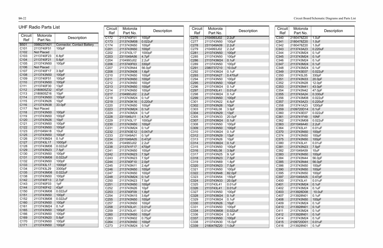
9A
-22 Circuit Board/Schematic Diagrams and Parts List
UHF Radio Parts List
Circuit Ref
Motorola Part No.
Description
B501 0986237A01 Connector, Contact Battery C101 2113740F51 100pFC102 Not PlacedC103 2113740F23 6.8pFC104 2113740F21 5.6pFC105 2113743N50 100pFC106 Not PlacedC107 2113740F17 3.9pFC108 2113743N50 100pFC109 2113740F51 100pFC110 2113743N50 100pFC111 2113740F30 13pFC112 2180605Z32 47pFC113 2180605Z16 10pFC114 2113743N50 100pFC115 2113743N26 10pFC116 2113743N38 33.0pFC117 Not PlacedC118 2113743N50 100pFC119 2113743N50 100pFC120 2113743N26 10pFC121 2113743N50 100pFC122 2113743N50 100pFC123 2311049A18 10uFC125 2113743N50 100pFC126 2113743M24 0.1uFC127 2113743L17 1000pFC128 2113743M08 0.022uFC129 2113743N23 7.5pFC130 2113743N50 100pFC131 2113743M08 0.022uFC132 2113743N50 100pFC133 2113743L17 1000pFC134 2113743L29 3300pFC135 2113743M08 0.022uFC138 2113743N50 100pFC142 2113740F13 2.7pFC143 2113740F03 1pFC144 2113740F42 43pFC150 2113743M08 0.022uFC151 2113743N50 100pFC152 2113743M08 0.022uFC160 2113743N50 100pFC161 2113743M24 0.1uFC165 2113743N50 100pFC166 2113743N50 100pFC169 2113743N20 5.6pFC170 2113743N50 100pFC171 2113743N50 100pF
C172 2113740F51 100pFC173 2113743M08 0.022uFC174 2113743N50 100pFC201 2113743N50 100pFC202 2113743L17 1000pFC203 2311049A56 4.7pFC204 2104993J02 2.2uFC206 2113740F63 330pFC207 2113743N44 56.0pFC208 2113743N08 1.6pFC210 2113743N50 100pFC211 2113743N50 100pFC212 2113743N50 100pFC213 2113743N50 100pFC214 2113743N50 100pFC217 2104993J02 2.2uFC218 2113743M24 0.1uFC219 2113743K16 0.220uFC220 2113743N50 100pFC223 2113743M24 0.1uFC224 2113743M24 0.1uFC228 2311049J11 4.7uFC229 2113743L17 1000pFC230 2113743N50 100pFC231 2113743M24 0.1uFC232 2113743E12 0.047uFC233 2311049A01 0.1pFC234 2311049A05 0.47pFC235 2104993J02 2.2uFC238 2113741F17 470pFC241 2113743N50 100pFC242 2113743N23 7.5pFC243 2113743N23 7.5pFC244 2113740F10 2.0pFC245 2113743N11 2.4pFC246 2113743N50 100pFC247 2113743N50 100pFC248 2113743M24 0.1uFC250 2113743N23 7.5pFC251 2113743N50 100pFC252 2113743N26 10pFC253 2113740F09 1.8pFC254 2113743N15 3.6pFC255 2113743N50 100pFC257 2113743N50 100pFC258 2113743L41 0.01uFC259 2113743L41 0.01uFC260 2113743N50 100pFC263 2113743N02 0.75pFC264 2113743N50 100pFC273 2113743M24 0.1uF
Circuit Ref
Motorola Part No.
Description
C276 2104993J02 2.2uFC277 2113743N50 100pFC278 2311049A09 2.2uFC279 2104993J02 2.2uFC281 2113743N50 100pFC285 2113743N50 100pFC286 2113743M24 0.1uFC289 2113743N50 100pFC291 2380737Z10 10.0uFC292 2113743M24 0.1uFC293 2113743A27 0.470uFC294 2113743N50 100pFC295 2113743N50 100pFC296 2113743M24 0.1uFC297 2113743L41 0.01uFC298 2113743M24 0.1uFC299 2113743N50 100pFC301 2113743N22 6.8pFC302 2113743N26 10pFC303 2113740L08 3.9pFC304 2113743N29 13pFC305 2113743N33 20.0pFC307 2113743M24 0.1uFC308 2113743N50 100pFC309 2113743N50 100pFC310 2113743M24 0.1uFC312 2113743N29 13pFC313 2113743N26 10pFC314 2113743M24 0.1uFC315 2113743N50 100pFC316 2113740L08 3.9pFC317 2113743N25 9.1pFC318 2113743N23 7.5pFC319 2113743N69 1.8pF C320 2113743N23 7.5pFC321 2113743N50 100pFC322 2113743N48 82.0pFC323 2113743N54 150pFC324 2113743N33 20.0pFC325 2113743L41 0.01uFC326 2113743L41 0.01uFC327 2113743N50 100pFC328 2113743M24 0.1uFC329 2113743M24 0.1uFC330 2113743N26 10pFC331 2113743N50 100pFC334 2113743M08 0.022uFC336 2113743M24 0.1uFC337 2113743N50 100pFC338 2113743N30 15.0pFC339 2180478Z20 1.0uF
Circuit Ref
Motorola Part No.
Description
C340 2180478Z20 1.0uFC341 2180478Z20 1.0uFC342 2180478Z20 1.0uFC343 2113743A23 0.220uFC344 2113743M24 0.1uFC345 2113743M24 0.1uFC346 2113743M24 0.1uFC347 2113743M24 0.1uFC348 2113743M24 0.1uFC349 2113743E07 0.022uFC350 2113743L05 330pFC351 2113743N33 20.0pFC352 2113743N28 12.0pFC353 2113743N41 43.0pFC354 2113743N42 47.0pFC355 2113743A24 0.330uFC356 2113743M08 0.022uFC357 2113743A23 0.220uFC358 2113741A23 1200pFC359 2109720D14 0.1uFC360 2113743E07 0.022uFC361 2113741F49 10NFC362 2113743M08 0.022uFC363 2311049A40 2.2uFC364 2113743L41 0.01uFC370 2113743N50 100pFC374 2113743N50 100pFC375 2113743N50 100pFC380 2113743L41 0.01uFC381 2113743N23 7.5pFC382 2311049A59 10uFC383 2113743N50 100pFC384 2113743N44 56.0pFC385 2113743N44 56.0pFC386 2113743N50 100pFC390 2113743N50 100pFC395 2113743N50 100pFC397 2311049A05 0.47pFC400 2113743L41 0.01uFC401 2113743M24 0.1uFC402 2113743M24 0.1uFC403 2113928D08 10.0uFC407 2113928N01 0.1uFC408 2113743N50 100pFC409 2113743M24 0.1uFC410 2113928N01 0.1uFC411 2113743M24 0.1uFC412 2113928N01 0.1uFC414 2113743M24 0.1uFC415 2109720D01 0.01uFC416 2113928N01 0.1uF
Circuit Ref
Motorola Part No.
Description

Circuit Board/Schematic Diagrams and Parts List
9A
-23
C420 2113743L41 0.01uFC421 2113928N01 0.1uFC422 2113743M24 0.1uFC423 2113743N50 100pFC424 2311049A59 10uFC425 2113743M24 0.1uFC426 2113743N50 100pFC427 2113743N50 100pFC428 2113743M24 0.1uFC429 2113743M24 0.1uFC430 2113928N01 0.1uFC431 2113743N50 100pFC433 2113743L41 0.01uFC434 2113743M24 0.1uF C435 2113743M24 0.1uFC436 Not PlacedC437 Not PlacedC440 2113743G26 4.7uFC441 Not PlacedC442 2113743E20 10uFC443 2113928N01 0.1uFC444 Not PlacedC445 Not PlacedC446 2113743R33 4700pF, 5%C447 2113743M08 0.022uFC448 Not PlacedC449 2113743N50 100pFC450 Not PlacedC451 2113743M08 0.022uFC452 2113743G26 4.7uFC453 2113743N50 100pFC456 2113743N50 100pFC458 2113743N50 100pFC459 2113743N50 100pFC463 2113743N50 100pFC466 2113743N50 100pFC467 2113928N01 0.1uFC471 Not PlacedC472 Not PlacedC473 2113743L09 470pFC475 2113743H14 10.0uFC476 2113928D08 10.0uFC477 2113743N50 100pFC478 2113743N50 100pFC479 2113928N01 0.1uFC480 2113928D08 10.0uFC481 2113928N01 0.1uFC482 2113928N01 0.1uFC483 2113743L17 1000pFC484 2113743L17 1000pFC485 2113743L17 1000pF
Circuit Ref
Motorola Part No.
Description
C486 2113743L17 1000pFC487 Not PlacedC488 2113743L17 1000pFC489 2113743L17 1000pFC493 Not PlacedC494 2113743N50 100pFC498 2113743N50 100pFC499 2113743N50 100pFC500 2113743L17 1000pfC501 2113743L17 1000pFC502 2311049A05 0.47pFC503 2113743N50 100pFC504 2113743L17 1000pFC505 2113743N50 100pFC506 2113743N50 100pFC507 2113743L17 1000pFC508 2113743N50 100pFC509 2113743L17 1000pFC511 2113743N50 100pFC512 2113743N50 100pFC513 2113743N50 100pFC514 2113743N50 100pFC515 2113743M24 0.1uFC518 2113743L17 1000pFC519 2113743L17 1000pFC520 2113743L17 1000pFC521 2113743L41 0.01uFC522 2113743L41 0.01uFC523 2113743N50 100pFC524 2113743L17 1000pFCR101 4880973Z02 Pin DiodeCR102 4802245J41 Pin DiodeCR105 5185963A15 Temperature Sense CR201 4802233J09 Diode TripleCR203 4862824C03 VaractorCR241 4805649Q13 Dual VaractorCR242 4862824C01 VaractorCR243 4862824C01 VaractorCR251 4802245J22 VaractorCR301 4862824C01 VaractorCR302 4862824C01 VaractorCR303 4880154K03 Dual Common Anode-Cath-
odeCR304 4862824C01 VaractorCR305 4862824C01 VaractorCR306 4802245J42 Ring Quad DiodeCR308 4802245J41 Pin DiodeCR310 4862824C01 VaractorCR411 4802245J47 Diode SchottkyCR412 4802245J47 Diode SchottkyCR413 4802245J47 Diode Schottky
Circuit Ref
Motorola Part No.
Description
CR440 4813833C02 Dual Diode Common CathodeCR501 4880107R01 RectifierCR503 4805729G49 LED Red/YelE101 2484657R01 Ferrite BeadE400 2480640Z01 Ferrite BeadF501 6580542Z01 Fuse 3AFL201 4802245J49 Crystal 16.8MHz ClipFL301 4802245J43 XTAL Filter 45.1MHzH101 2680499Z01 Heat SpreaderJ101 0180117S05 RF Jack AssemblyJ104 3980686Z01 Antenna ContactJ400 0905505Y04 40-Pin ConnectorJ402 2809926G02 4-Pin ConnectorJ404 0980689Z01 Connector (Stereo Jack
2.5mm)J407 0980688Z01 Connector (Mono Jack
3.5mm)L101 2460591B48 15.22nH, 10%L102 2460591B48 15.22nH, 10%L104 2460591B48 15.22nH, 10%L105 2462587N22 390nHL106 2479990A02 7.66nHL107 2479990G01 33.47nHL108 2479990A01 4.22nHL112 2462587N45 22nHL113 2413926H09 5.6nHL114 2462587N22 390nHL115 2462587N22 390nHL116 2479990A03 9.75nHL160 Not PlacedL201 2462587Q20 2.2uHL202 2462587Q20 2.2uHL203 2462587Q20 2.2uHL232 2462587P25 12uHL241 2462587V41 390nHL242 2462587V38 220nHL243 2460593C01 Teflon ResonatorL251 2462587V28 33nHL253 2460593C02 Teflon ResonatorL261 2462587V29 39nHL271 2462587V32 68nHL273 2462587V28 33nHL281 2462587V41 390nHL282 2462587V41 390nHL301 2479990C01 13.9nHL302 2479990C01 13.9nHL303 2462587V26 22nHL304 2462587V37 180nHL305 2462587V26 22nHL306 2479990C01 13.9nHL307 2479990C01 13.9nH
Circuit Ref
Motorola Part No.
Description
L309 2479990C02 16.28nHL310 2462587V36 150nHL311 2462587N65 750nHL314 2462587N72 2.2uHL325 2480646Z20 2.20uHL330 2462587N64 680nHL331 2480646Z20 2.20uHL332 2462587N53 100nHL340 2462587V41 390nHL400 2462587Q42 390nHL410 2462587Q42 390nHL411 2462587Q42 390nHL505 2462587Q42 390nHPB501 4080523Z01 Tactile Push ButtonPB502 4080523Z01 Tactile Push ButtonPB503 4080523Z01 Tactile Push ButtonQ110 4802245J55 RF Power FETQ111 4802245J50 Dual NPN/PNP Q210 4802245J50 Dual NPN/PNP Q241 4805218N63 NPNQ260 4802245J50 Dual NPN/PNP Q261 4802245J50 Dual NPN/PNP Q301 4802245J44 NPNQ302 4802245J44 NPNQ315 4880214G02 NPNQ320 4805218N63 NPNQ400 4809579E18 MOSFET P-CHAN Q403 4880214G02 NPNQ405 4802245J54 Dual NPNQ410 4802245J54 Dual NPNQ417 4802245J50 Dual NPN/PNP Q418 4802245J50 Dual NPN/PNP Q419 5180159R01 Dual NPNQ420 4805128M67 SOT STR MMBTQ421 4880214G02 NPNQ431 5180159R01 Dual NPNQ502 5180159R01 Dual NPNQ503 4802245J50 Dual NPN/PNPQ505 4880214G02 NPNR101 0662057A34 240R102 0680735Z01 0.075R103 0662057M41 43R104 0662057N15 47KR105 0662057M01 0R106 0662057M26 10R108 0662057M92 5.6KR109 0662057N30 200KR110 0662057M61 300R111 0662057M33 20R112 0662057M61 300R120 0662057N14 43K
Circuit Ref
Motorola Part No.
Description

9A
-24 Circuit Board/Schematic Diagrams and Parts List
* Motorola Depot Servicing only
R130 0662057M98 10KR131 0662057N14 18KR132 0662057N33 270KR134 0662057N52 1.6MR161 0662057M57 200R170 0662057A34 240R171 0662057N14 43KR172 0662057A32 200R173 0662057N29 180KR201 0662057N21 82KR202 0662057N23 100KR204 0662057N15 47KR231 0662057M52 120R232 0662057M69 620R233 0662057M68 560R241 0662057M32 18R242 0662057M57 200R243 0662057M98 10KR244 0662057N01 12KR245 0662057M59 240R248 0662057M37 30R251 0662057M32 18R252 0662057M62 330R253 0662057M95 7.5KR254 0662057M95 6.8KR255 0662057M89 4.3KR256 0662057M37 30R260 0662057M74 1KR281 Not PlacedR300 0662057M82 2.2KR301 0662057N23 100KR302 0662057N23 100KR303 0662057M89 1KR304 0662057N01 12KR305 0662057M67 0R306 0662057N23 100KR307 0662057N23 100KR308 0662057M42 47R309 0662057M01 0R310 0662057M60 270R311 0662057N10 30KR312 0662057M92 5.6KR313 0662057M62 330R314 0662057M85 3KR315 0662057N01 12KR316 0662057A96 91KR317 0662057M74 1KR318 0662057A79 18KR319 0662057A29 150R320 0662057M74 1KR321 0662057M83 2.4K
Circuit Ref
Motorola Part No.
Description
R322 0662057N30 200KR324 0662057M81 2KR325 0662057M94 6.8KR327 0662057N11 33KR328 0662057M01 0R329 0662057M01 0R339 0662057M01 0R340 0662057M94 6.8KR342 0662057N23 100KR343 0662057M26 10R344 0662057N01 12KR345 0662057M98 10KR346 0662057N17 56KR347 0662057M74 1KR348 0662057M87 3.6KR349 0662057C01 0R350 0662057N23 100KR351 0662057C01 0R352 0662057M86 3.3KR355 0662057M01 0R400 0662057N15 47KR401 0662057M01 0R405 0662057M01 0R406 0662057N20 75KR410 0662057N23 100KR411 0662057M98 10KR413 0662057M01 0R414 0662057V34 180KR415 0662057V26 91KR416 0662057N13 39KR418 0662057M01 0R419 0662057M67 0R423 0662057N39 470KR425 0662057N10 30KR427 0662057M98 10KR428 0662057M10 2.2R429 0662057M98 10KR432 0662057N16 51KR434 Not PlacedR435 0662057M81 2KR436 0662057N15 47KR438 0662057M01 0R445 0662057N08 24KR446 0662057N31 220KR447 0662057N51 1.5MR448 0662057N33 270KR449 0662057N08 24KR457 0662057M98 10KR460 0662057M90 4.7KR461 0662057N23 100KR462 0662057N23 100K
Circuit Ref
Motorola Part No.
Description
R463 0662057M61 300R471 0662057M92 5.6KR472 0662057N12 36KR473 0662057M26 10R475 0662057M01 0R476 0662057N08 24KR478 0662057M98 10KR481 0662057N08 24KR492 0662057M01 0R494 0662057M01 0R495 0662057N23 100KR496 0662057N23 100KR498 0662057N23 100KR499 0662057M98 10KR501 0662057M70 680R502 0662057M56 180R505 0662057M98 10KR506 0662057N15 47KR507 0662057M01 0RT300 0680590Z01 Thermistor_33KRT400 0680590Z01 Thermistor_33KS501 4080710Z01 Channel SwitchS502 1880619Z01 Volume SwitchSH100 2680687Z01 Shield, Harmonic FilterSH101 2680510Z01 Shield, PASH201 2680511Z01 Synthesizer Top ShieldSH202 2680511Z01 Synthesizer Bottom ShieldSH241 2680513Z01 Shield, VCO TopSH242 2680514Z01 Shield, VCO Bottom/LVZIFSH301 2680554Z01 RX Pre Filter ShieldSH302 2680555Z01 RX Post Filter/RX AMPSH303 2680509Z01 Shield, MixerSH304 2680624Z01 Shield, Mixer DiodeSH321 2680508Z01 Shield, LVZIF 2ND LOSH322 2680514Z01 ZIF ShieldSH323 2680553Z01 Shield, Crystal FilterSH400 2680505Z01 Controller Memory ShieldSH401 2680506Z01 On/Off Controller ShieldSH402 2680515Z01 Microprocessor Controlled
ShieldSH403 2680516Z01 ASFIC CMP/Audio PA Con-
troller ShieldT301 2580541Z01 XFMR CoilT302 2580541Z01 XFMR CoilU101 5105109Z67 LDMOS Driver UHF ICU102 5185765B01 Power Control ICU201 5185963A27 LVFRACNU210 5102463J61 Inverter U211 5102463J61 Inverter U241 5105750U54 VCO BufferU247 5105739X05 Regulator Linear
Circuit Ref
Motorola Part No.
Description
U248 5102463J58 3.3V Regulator U301 5109632D83 LVZIF 2.2U400 5102463J40 3.3V Regulator U404 5185963A53 ASFIC CMP U405 Not PlacedU406 *5102463J59 Flash ROM 128K x 8U407 *5102463J64 16K x 8 EEPROMU409 5102226J56 UP HC11FLOU410 5102463J57 Regulator 3.3VU420 5102463J44 Audio PAVR432 4805656W08 5.6V ZenerVR433 4805656W08 5.6V ZenerVR434 4802245J51 Zener 6.8VVR439 4880140L15 10V ZenerVR440 4802245J51 Zener 6.8VVR441 4802245J51 Zener 6.8VVR442 4802245J51 Zener 6.8VVR443 4802245J51 Zener 6.8VVR444 4802245J51 Zener 6.8VVR445 4802245J53 Zener_10VVR446 4802245J53 Zener_10VVR447 4802245J53 Zener_10VVR448 4802245J53 Zener_10VVR449 4802245J53 Zener_10VVR450 4802245J53 Zener_10VVR501 4813830A18 6.8V ZenerVR506 4802245J51 Zener 6.8V
7580671Z01 Pad (Flexible Circuit)8480672Z01 UHF B1 PC Board
Circuit Ref
Motorola Part No.
Description

Circuit Board/Schematic Diagrams and Parts List
9A
-25
8.0 Circuit Board/Schematic Diagrams and Parts List
ZMY0130320 -B
TP401
40
J400
1
U405
17
8 21
22
C426 C425
C423
R418
R437
R410
U406
116
1732
C427 C428
C429
C424R408
R492
R429
R478
R428
SH400
8
5 4
1
U407
C432
FL201
1 3
46
TP201
SH201
C52
3
C52
5
C527C51
5
C52
4
C52
6
C528
C44
6
C45
5
Q50634
R51
0VR431VR450
VR451
FL301
C324C323
L311C220
C294
C23
5
C29
1
L203
U247
C203
L232C210
C211C212
C213
C21
4
C230
C25
6
C257
C260
C29
9
C292
C22
9
C217
C228
C23
3
C238
C29
7
CR201
L201
L202
Q210
34
Q26034
R256
R255
TP410
5
6
4
3
1
2J402
C470
C471
C472
C483
C484
C485
CR413
Q41734
Q433
Q431
R493 R494
R499
R498
RT400
TP402
TP405 TP406 TP415
SH401
C401
C402
C400
C467
C482
C403
C480
CR412
CR440
Q400
Q403
Q405
34
R401R402
R403
R405
R454
R455R456
R416
R427
R448R447
R452
R406R476
R481
R446
R451
U400
85
4
C247C251
C285
C289
C370
C374
C386
C248 C273
C286
C276
C253
C271C272
L282
3
L243
1
L2733
L253
1
L271
L321
Q26134
Q241
R333
R339
R243
R248
R253
R260
SH241
C109C110
C114
C118 C119
C121
C122C125
C160
C165
C166
C171
C111
C112
C113
C115
C120
C116
C117
C161
C127
C131C129C169L114
L115
L106
L107
L108
L113
L160
3
2
Q110
1
R103
R104
R175R105
R106R107
R108
R120
R171
R161
R173
R176
R177
SH101
U101
9
8
16
1
C325
R351
R352
SH323
PB504
C397
R300VR444
C328
C391
Q315
Q316
R326
R314R316
R318
R319
R325
R327
R334
R335
R338
RT300
RT301
VR300
C351
C362
C364
C363
C349C350
C352C353
C354C384
C385
CR310
L325
L332
Q320
R355
R322
R345
R320
R321
R324
R346
SH321
C375 C320C319
L309
R348
T302
34
6
TP202
TP302
SH303
C381
C322
L310R309
R308
R310
T301
3 4
6
C331
C396
C333
CR308
R342
R317
R336
C308
C302
C305
C301
C303
C304
CR301
CR302
L301
L302
R301
R302
SH301
C108
C454
C498
C499C518
C519
C520
Q111
34
R101
R170
VR432
VR433
5
7
4
J407
6
3
2
C140
C477
C478 C508
C511 C514
C501C504
C509
C141
CR160
L116
C505
C502
C521 PB501PB502
VR440
VR501
C512
C513
CR5032
34Q502
R501
R502
C506
C507
Q505
R506R507
R505
UHF (403-470MHz) Main Board Top Side PCB No. 8480672Z04

9A
-26 Circuit Board/Schematic Diagrams and Parts List
5
2S502
3
4
4
C
8
CS501
2
J104
J101
4
3
2
1
C101
C102
C107C103
C104
C106
C142
C143
C144
CR101
CR10
2
L101
L102
L104
L105
SH10
0
C172
C132
C173
CR105
H101
R133
R172
C309
C315
C321
C395
C313
C307
C310
C314
C318
C380C306
C311
C316C3
12C317
CR304
CR305
CR30
3 L340
L306 L307L303
L305L304Q30
1
R328 R3
06
R307
R304
R303R347
R305
R340
SH302
C337
C383
C390
C329
C336
C344
C345
C346
C347 C3
48
C334
C356C3
39
C340
C341
C342
C343
C357
C360
C355
C358
C359
C361
C382
L314
L331
R343
R350R344
SH322
1325
37 1
U301
1
2
3
B501
C327
C330
C326
C338
L330
Q302
R312
R315
R313
R311
C277
C279
C522
C278
C280
CR501
L505
U248
VR441
VR506
VR43
9
C500
C503
CR306
F501
SH304
C130
C138 C151
C170
C123
C126
C128
C150C152
E101
L112R102
R329
C105 C1
74
C133
C135
C134
R109
R130
R131 R132
R134
25
917
U102
1
C201
C264
C218
C223
C224
C231
C296
C298
C202
C204
C206C2
07
C208
C219
C232
C234 C258
C259
C263
C265
C293
CR203L261
R204
R281R201
R202
R231
R232
R233
SH202
13
2537
1
U201
U2103 4
U2113
4
C431
C494
C435
C489
C433
CR41
4
Q418
3
R463
R414
R415
R460
51
U410
Q419
C434
R461R462
R419
U409
761
C453
C456
C493
L411
R411 R457
R432
E400
L410
C449
C463
C486
C488
26
C241
C246
C255
C281
C295
C372
C252
C242
C243
C250
C244
C245C254
C371
C373
C378
CR241
CR242
CR243
CR251
L241
L281L242
L251
Q310R349
R330
R332
R110
R112
R111
R241
R251
R242
R244
R245
R252
R254
R331
SH242
U241
10
201
11 C408
C487
C409
C411
C414
C422
C450C451
C420
C419
C407
C410
C412
C416
C421
C430
C443
C447
C479
C481
C476
C415
C442
C452
C475
Q410
34
R400R473R4
13
R475
R471
R425 R423
R445
R449
R472
SH403
13
2537
1
U404 U420
10
20
1
11
C458
C459
C466
C440
C473L400
Q421
Q420
R436
R438
R467
R439
R495
R496
R435
R434
ZMY0130319 -B
UHF (403-470MHz) Main Board Bottom Side PCB No. 8480672Z04

Circuit Board/Schematic Diagrams and Parts List
9A
-27
MECH_SWB+
C5020.47uF
7TAB2
2
S5024
LOW
HIGH
36
TAB1
mgc_comps
1
5
CR501
UNSWB+
Vdda
R5070
1
24VF501
3A2
C5001000pF
C503100pF
10VVR439
BATT_CODE
2RSSI_FIL
1NEG
3POS
B501
6.8V
L505390nH
VR506
100pFC505
VR5016.8V
VOL
RED_LED2
4
3
51
6
IMX1
SWB+
Q502
Q505
R50510K
R50647K
C507100pFC506
1000pF
GREEN_LED
Vdda
180R502
680R501
CR503 1
2
3
4
RTA3
RTA2
RTA0RTA1
C511100pF
C513100pF
C512100pF
C514100pF
PC01
PC12PC2
PC3
SWITCH
C0C0C1 C1
GND GND1
SWITCHS501
4 8
97
5V
SWITCH
12
PB502
VR4446.8V
.01uFC522
VR4416.8V
C521.01uF
12
PB501SWITCH
PB504SWITCH
12
6.8VVR440
SB1
PTT
SB2
J407
S1
S2
S3
S4
M1
M2
M3
C525 C528100pFC527C526
1000pF 1000pF100pF
ANT_BIAS
C509C508 C501100pFC477
100pF 1000pF1000pF 1000pFC504C478
100pF
SCI
C5150.1uF
C5241000pF
C523100pF
Q506
10K
47K
47K4.7K
100pFC454
1000pFC520
470pFC455
.022uFC446
100pFC498
100pFC499
1000pFC518 C519
1000pF10VVR4332
3
11
VR43210V
23
VR45010.0V
VR45110.0V
SPN
INT_SPN
SPP
MIC
INT_MIC
6.8VVR431
R51010K
ZMY0130312-D
UHF Controls And Switches Schematic Diagram

9A
-28 Circuit Board/Schematic Diagrams and Parts List
RXFE Top Shield RXFE Bottom Shield Mixer Shield
RX Mixer Diod Shield
100KR302
L30113.9nH
CR301 CR302
L30213.9nH
6.8pFC301
10pFC302
100KR301
3.9pFC303
RX_IN0.1uFC307C305
20pF
6.8KR340L303
22nH
C308100pF
3
1
CR303
2C30413pF
4.3KR303
0R328
0.1uFC310
R30412K
100pFC309
100pFC321
510R305
0.1uFC314
L304180nH
13
2
Q301
100pFC315
C306NU
C311NU
L30522nH
10pFC313
C3187.5pF
100KR307
C31213pF
100KR306
CR304
13.9nHL306
3.9pFC316
CR305
9.1pFC317L307
13.9nH
R3471K
1
HSMP3820CR308
2
3
100pFC395
L340390nH
R5
R5
1KR317
C331100pF
Q315
13
2
C333
R336
NU
NU
R31691K
C396NU
R31818K
150R319
33KR327 RT300
33.0K
2
1
R334R326
R3256.8K
VR300Q316
13
2NU
NU
NUNU
R335
8.2KR338
C3910.1uF 33.0K
RT301
2 1
R5
NU
NUNU
R3002.2K
C3970.47uF
RSSI
SHIELDSH303
if1
if1
SHIELDSH304
SH302SHIELD
if1
SH301SHIELD
if1
C32282pF
R3090
270R310
150nHL310
47R308
IF
XFMR
4
6
3
1
2
T301
CR306
2
34
1
C3817.5pF
46
31 2XFMRT302
3.6KR348
C3191.8pF
16.28nHL309
TP302
100pFC375C320
7.5pF
0R339
R5
C374100pF
0R349
C386100pF
L321 R333NU NU
13
2
Q310NU
C373 C378NU NU
RX_INJ
R332
100pFC370
NU
R331C371 C372R330NU NU NU NU
R5R342100K
.01uFC380
DACRx
0R329
VCO
ZMY0130315-E
UHF Receiver Front End Schematic Diagram

Circuit Board/Schematic Diagrams and Parts List
9A
-29
CRYSTAL FILTER SHEILD LVZIF TOP SHIELD LVZIF BOTTOM SHIELD
(SOURCE)
2.20uHL331
10R343
C38210uF
VddaVdd_FILTERED
C3440.1uF
C3480.1uF 0.1uF
C347
C3290.1uF
C3430.22uF
C3391uF
C3401uF
1uFC342
1uFC341
0.22uFC357
32V
AG
25V
AG
_RE
F
RE
D_V
CC
RE
D_V
SS
30R
OS
E_V
CC
29R
OS
E_V
SS
RS
SI_
FLT
RS
SI_
OU
T
16TESTA
31
42MIX_BYP
MIX_IN46
24MLPD_CR
26P
HA
SE
_LO
CK
47PREAMP_OUT
48PRE_AGC
21FREF
20GND
GO
LD_V
CC GOLD_VSS
41GREEN_VCC
43GREEN_VSS
15IOUT
LIM
37C4P
19CEX
18CLK
17DATA
28D
EM
OD
_HF
27D
EM
OD
_OU
T
23BRP_OFF
33C
1M
40C1P
34C
2M
39C2P
35C
3M
38C3P
36C
4M
32D83U301
45BLUE_VCC
44BLUE_VSS
22BROWN_VCC
9V
PP
1 2 54 8T
ES
TD
3P
RE
_IN
6E
XT
BS
10 11E
MIT
7A
FC
12B
AS
E
1413COL
0.33uFC355
.022uFC356
C33815pF
Vdd_FILTERED
100pFC337
0.1uFC336
L3142.2uH
0.1uFC328
R3143K
330R313
.01uFC326
R5
Q302
R3125.6K
C33010pF
R31130K
C327100pF
L330680nH12K
R315
DA
RSSI
.01uFC361
R3523.3K
C325.01uF
2G
ND
14
GN
D2
5G
ND
3
3OUT6 IN
FL301XTALTBD
1G
ND
0R351
C32420pF
750nHL311150pF
C323
IF
100pFC390
100KR350C345
0.1uF
R34412K
C3460.1uF
DB
DEMOD
1200pF
C3590.1uF
C358
.022uFC334
16.8MHz
CLKDATA
LVZIF_SEL
20pFC351
12pFC352
.022uFC349
330pFC350
100pFC383
Vdd_FILTERED
R3550
56KR346
47pFC354
1
3
2
Q320BFQ67W
C38456pF
R3242K
R34510K
43pFC353
CR3101K
R320
R322200K
2.20uHL325
C364.01uF2.4K
R321
C38556pF
.022uFC362
L332100nH
C3632.2uF
1 if
SHIELDSH322
if
SHIELDSH323
1
.022uFC360
if
SHIELDSH321
1
ZMY0130314-D
UHF Receiver Back End Schematic Diagram

9A
-30 Circuit Board/Schematic Diagrams and Parts List
.01uFC258
.01uFC259
100pFC256
100pFC299
C2960.1uF
2
NC
VCC5
U210TC7ST04FU
GND3
41NC
1 4
VCC5
U211TC7ST04FU
GND3
2
C265100pFC257
NU
100pFC230
K33
6A1
5A2
4A3
1K1
K22
CR201
C229 C2281000pF 4.7uF
C2980.1uF
L2022.2uH
C2190.22uF
5V(SOURCE)
0.1uFC292
NR2
OUT4
SD3
U247ADP3300
ERR6 G
ND
1
IN5
2.2uFC235
0.1uFC223
10.0uFC291
2.2uHL203
2.2uHL201
Vdda
0.1uFC224
C294100pF
C2930.47uF
SWB+
LP2980U248
2GND
4
NC
ON
_OF
F*
3 1
VIN
5
VO
UT
C277100pF
C2782.2uF
4V_3.3V
2.2uFC217
C2802.2uFC220
100pFC2180.1uF 2.2uF
C279
MODOUT
0.47uFC234
1
120R231
TP202
.047uFC232R256
30
C2330.1uF
4.3KR255
16.8MHz
Q210
2
4
1
3
C260100pF
R5
5V
47K
47K4.7K
10KAUX3
AUX4
TP2011
47KR204
C213100pF
LOCK
R233560
0.1uFC231
620R232
470pFC238
12uHL232
GND1 4
GND1
3OUT
6IN
75Z04FL201
C20839pFC207
C206330pF
CR203
R281NU
NU
if
SH201SHIELD
1
SYNTHESIZER TOP SHIELD
1 if
SH202SHIELD
SYNTHESIZER BOTTOM SHIELD
DATA
CSXCLK
MODIN
C212100pF
C214100pF
C210100pF 100pF
C211
L26139nH 100pF
C264
PRESC
C2630.75pF
82KR201
R202100K
VSF
C2042.2uF
15VMULT1
14VMULT2
VMULT312
11VMULT4
13V
RO
WARP25
23XTAL1
24XTAL2
27SFBASE
26SFCAP
30SFIN
28SFOUT
37TEST1
38TEST2
21VBPASS
47V
CP
31NC3
44P
D_G
ND
5P
D_V
DD
32PREIN
33P
RE
_GN
D
34P
RE
_VD
D
35PVREF
18REFSEL
45IADAPT
16INDMULT
43IOUT
4LOCK
10MODIN
41MODOUT
17NC1
29NC2
39BIAS2
CCOMP42
9CEX
8CLK
7DATA
6D
GN
D
36D
VD
D
19FREFOUT
46ADAPTSW
22A
GN
D
48AUX1
1AUX2
2AUX3
3AUX4
20A
VD
D
40BIAS1 U201
63A27
1000pFC202
100pFC201 C203
4.7uF
VCTRL
ZMY0130316-D
UHF Synthesizer Schematic Diagram

Circuit Board/Schematic Diagrams and Parts List
9A
-31
100pFC281 R245
240
L281390nH
TX_INJ
RX_INJ
33nHL273
68nHL271
0.1uFC273
C2762.2uF
C2860.1uF
VSF
TX_OUT
TX_SWITCH
RX_OUT
RX_SWITCH
PRESC_OUT
10
13
8
7
12
14
VC
C_B
UF
FE
RS
18
VC
C_L
OG
IC
Rx_sw
PRESC
Tx_sw
1TX_IADJ
6RX_EMITTER
2RX_IADJ
3SUPER_FLTR
19TRB_IN
16TX_BASE
15TX_EMITTER
4COLL_RFIN
20FLIP_IN
11G
ND
_BU
FF
ER
S9
GN
D_F
LAG
GN
D_L
OG
IC17
5RX_BASE
50U54
U241
C289100pF
1KR260
DD
AUX42
1
34
Q261
AUX3
5V
DUMMY
VCO TOP SHIELD VCO BOTTOM SHIELD
if
SH241SHIELD
1 if
SH242SHIELD
1
C297.01uF 1
3
2
4
Q260
C272
C271
NU
NU
C246100pF
18R241
C285100pF
200R242
RESONATOR
L243
3
C2507.5pF
1
2
C2427.5pF
C2437.5pF
C2452.4pF
10KR243
Rx_sw2pFC244
CR243
VSF
12KR244
1
3
2BFQ67W
Q241
390nHL282
30R248
R2537.5K
Tx_sw100pFC247
R2547.5K
3.6pFC254
C2480.1uF
10pFC252
33nHL251
CR2511.8pFC253
P1 1
RESONATOR
L253
2
P2
3P3
R25118
R252330
C255100pF
10K
4.7K
47K
47K
CR242
CR241
L242220nH
390nHL241
C241100pF
VCTRL
100pFC251
1 2
ZMY0130318-D
UHF Voltage Controlled Oscillator Schematic Diagram

9A
-32 Circuit Board/Schematic Diagrams and Parts List
TX_OUT
C109100pF
L1067.66nH
UNSWB+
15pFC111
10pFC113
51pFC112
E101BEAD
0.1R102
10uFC123 L107
33.47nH
C172100pF
Microstrip Microstrip
Q1101
2
3
6.2R177
R1766.2
200R172
100pFC114
20pFC116
10R106
4.22nHL108
C115 C11730pF
100pFC118
R1050
NU
TX_INJ
C12010pF
22nHL112
100pFC121
100pF
15.0nHL160
C160
UNSWB+
.022uFC128C130
100pF
R1085.6K
.022uFC150R107 C151
100pFNU
R16175
TX_INJ_1
300R112
100pFC125SH101
SHIELD
1 if
H101HEATSINK
1POS
R173180K
43KR120
100pFC119
100pFC171 R171
43K
R17547K
300R110
43R103
R11120
100pFC295
R10447K
RF
OU
T2
7
VC
NT
RL
1
VD
1
14
VG
1
2
VG
2
3
GND312
GND413
NC
1
8
NC
2
9
NC
3
10
NC
4
15
RF
IN
16
RF
OU
T1
6
G2
11
GND14
GND25
30C65U101
0.1uFC161
C152.022uF
L1135.6nH
C131.022uF
C1695.6pF
100pFC166 R132
270K
C1297.5pF
390nHL1141000pF
C127
C165100pF
UNSWB+FROM_RF
1000pFC133
L115390nH
C1343300pF
C135.022uF
R1341.6MEG
R109200K
C174100pF
ANT_BIAS
UNSWB+
DATA
CLK
CSX
100pFC105
100pFC122
4
1
3
Q111
2
6
10K
47K
47K
4.7K
UNSWB+
C132100pF
TX_BIAS
R133NU
20
VAR218
VAR324
15V
G
6VL
19VLIM
RS
RS
ET
31
23RX
2T1
30T
EM
P
14V
10
16V
45
V5EXT17
VAR1
F16
8
8GND1
25G
ND
2
4INT
NA22
11Q
10Q
X
RFIN1
21
CE
X
3CI
5CJ
7CL
26C
LK
12C
Q13
CQ
X28
DA
TA
9
H99S-4U102
32A
NO
27B
PO
S
29
100pFC138
0.1uFC126
CR105LM50
100pFC170
5V
R13010K
3GND
PO
S1
VOUT2
18KR131
C173.022uF
100pFC110
RESET
ZMY0130317-D
UHF Transmitter Schematic Diagram

Circuit Board/Schematic Diagrams and Parts List
9A
-33
HF SHIELD
4GND
J101RF_JACK
1
2
3
RF
_JA
CK
C140
ANTENNA_CONTACT
J104
NU
C101100pF
L11617.02nH 3.3pF
C141
L10115.22nH
C102
2.7pFC142
NU
15.22nHL102
C1045.6pF
C1036.8pF
1pFC143
100pFC108
ANT_BIAS
390nHL105
TX_OUT
CR101
15.22nHL104
RX_IN
C1073.9pF
C106 2
3
1
NU
CR102
240R101
240R170
if
SH100SHIELD
1
43pFC144
A1
A2
A3
K1
K2
K3
CR160
ZMY0130313-C
UHF Harmonic Filter Schematic Diagram
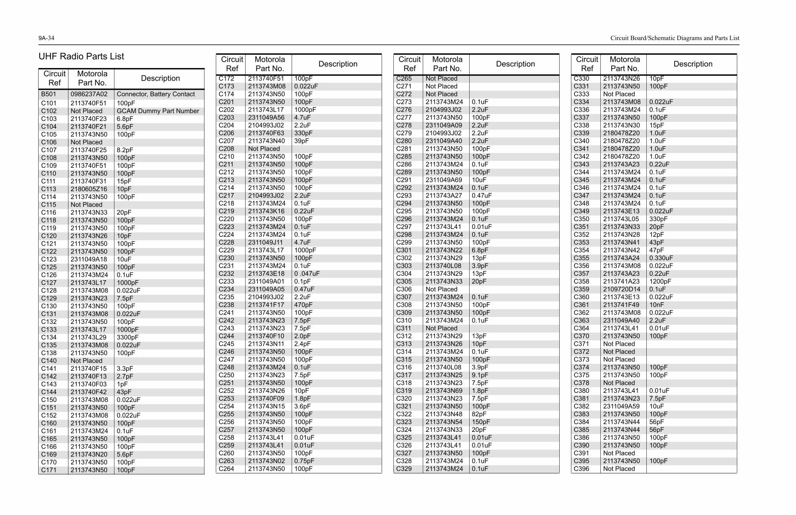
9A
-34 Circuit Board/Schematic Diagrams and Parts List
UHF Radio Parts List
Circuit Ref
Motorola Part No.
Description
B501 0986237A02 Connector, Battery ContactC101 2113740F51 100pFC102 Not Placed GCAM Dummy Part NumberC103 2113740F23 6.8pFC104 2113740F21 5.6pFC105 2113743N50 100pFC106 Not PlacedC107 2113740F25 8.2pFC108 2113743N50 100pFC109 2113740F51 100pFC110 2113743N50 100pFC111 2113740F31 15pFC113 2180605Z16 10pFC114 2113743N50 100pFC115 Not PlacedC116 2113743N33 20pFC118 2113743N50 100pFC119 2113743N50 100pFC120 2113743N26 10pFC121 2113743N50 100pFC122 2113743N50 100pFC123 2311049A18 10uFC125 2113743N50 100pFC126 2113743M24 0.1uFC127 2113743L17 1000pFC128 2113743M08 0.022uFC129 2113743N23 7.5pFC130 2113743N50 100pFC131 2113743M08 0.022uFC132 2113743N50 100pFC133 2113743L17 1000pFC134 2113743L29 3300pFC135 2113743M08 0.022uFC138 2113743N50 100pFC140 Not PlacedC141 2113740F15 3.3pFC142 2113740F13 2.7pFC143 2113740F03 1pFC144 2113740F42 43pFC150 2113743M08 0.022uFC151 2113743N50 100pFC152 2113743M08 0.022uFC160 2113743N50 100pFC161 2113743M24 0.1uFC165 2113743N50 100pFC166 2113743N50 100pFC169 2113743N20 5.6pFC170 2113743N50 100pFC171 2113743N50 100pF
C172 2113740F51 100pFC173 2113743M08 0.022uFC174 2113743N50 100pFC201 2113743N50 100pFC202 2113743L17 1000pFC203 2311049A56 4.7uFC204 2104993J02 2.2uFC206 2113740F63 330pFC207 2113743N40 39pFC208 Not PlacedC210 2113743N50 100pFC211 2113743N50 100pFC212 2113743N50 100pFC213 2113743N50 100pFC214 2113743N50 100pFC217 2104993J02 2.2uFC218 2113743M24 0.1uFC219 2113743K16 0.22uFC220 2113743N50 100pFC223 2113743M24 0.1uFC224 2113743M24 0.1uFC228 2311049J11 4.7uFC229 2113743L17 1000pFC230 2113743N50 100pFC231 2113743M24 0.1uFC232 2113743E18 0 .047uF C233 2311049A01 0.1pFC234 2311049A05 0.47uFC235 2104993J02 2.2uFC238 2113741F17 470pFC241 2113743N50 100pFC242 2113743N23 7.5pFC243 2113743N23 7.5pFC244 2113740F10 2.0pFC245 2113743N11 2.4pFC246 2113743N50 100pFC247 2113743N50 100pFC248 2113743M24 0.1uFC250 2113743N23 7.5pFC251 2113743N50 100pFC252 2113743N26 10pFC253 2113740F09 1.8pFC254 2113743N15 3.6pFC255 2113743N50 100pFC256 2113743N50 100pFC257 2113743N50 100pFC258 2113743L41 0.01uFC259 2113743L41 0.01uFC260 2113743N50 100pFC263 2113743N02 0.75pFC264 2113743N50 100pF
Circuit Ref
Motorola Part No.
Description
C265 Not PlacedC271 Not PlacedC272 Not PlacedC273 2113743M24 0.1uFC276 2104993J02 2.2uFC277 2113743N50 100pFC278 2311049A09 2.2uFC279 2104993J02 2.2uFC280 2311049A40 2.2uFC281 2113743N50 100pFC285 2113743N50 100pFC286 2113743M24 0.1uFC289 2113743N50 100pFC291 2311049A69 10uFC292 2113743M24 0.1uFC293 2113743A27 0.47uFC294 2113743N50 100pFC295 2113743N50 100pFC296 2113743M24 0.1uFC297 2113743L41 0.01uFC298 2113743M24 0.1uFC299 2113743N50 100pFC301 2113743N22 6.8pFC302 2113743N29 13pFC303 2113740L08 3.9pFC304 2113743N29 13pFC305 2113743N33 20pFC306 Not PlacedC307 2113743M24 0.1uFC308 2113743N50 100pFC309 2113743N50 100pFC310 2113743M24 0.1uFC311 Not PlacedC312 2113743N29 13pFC313 2113743N26 10pFC314 2113743M24 0.1uFC315 2113743N50 100pFC316 2113740L08 3.9pFC317 2113743N25 9.1pFC318 2113743N23 7.5pFC319 2113743N69 1.8pFC320 2113743N23 7.5pFC321 2113743N50 100pFC322 2113743N48 82pFC323 2113743N54 150pFC324 2113743N33 20pFC325 2113743L41 0.01uFC326 2113743L41 0.01uFC327 2113743N50 100pFC328 2113743M24 0.1uFC329 2113743M24 0.1uF
Circuit Ref
Motorola Part No.
Description
C330 2113743N26 10pFC331 2113743N50 100pFC333 Not PlacedC334 2113743M08 0.022uFC336 2113743M24 0.1uFC337 2113743N50 100pFC338 2113743N30 15pFC339 2180478Z20 1.0uFC340 2180478Z20 1.0uFC341 2180478Z20 1.0uFC342 2180478Z20 1.0uFC343 2113743A23 0.22uFC344 2113743M24 0.1uFC345 2113743M24 0.1uFC346 2113743M24 0.1uFC347 2113743M24 0.1uFC348 2113743M24 0.1uFC349 2113743E13 0.022uFC350 2113743L05 330pFC351 2113743N33 20pFC352 2113743N28 12pFC353 2113743N41 43pFC354 2113743N42 47pFC355 2113743A24 0.330uFC356 2113743M08 0.022uFC357 2113743A23 0.22uFC358 2113741A23 1200pFC359 2109720D14 0.1uFC360 2113743E13 0.022uFC361 2113741F49 10nFC362 2113743M08 0.022uFC363 2311049A40 2.2uFC364 2113743L41 0.01uFC370 2113743N50 100pFC371 Not PlacedC372 Not PlacedC373 Not PlacedC374 2113743N50 100pFC375 2113743N50 100pFC378 Not PlacedC380 2113743L41 0.01uFC381 2113743N23 7.5pFC382 2311049A59 10uFC383 2113743N50 100pFC384 2113743N44 56pFC385 2113743N44 56pFC386 2113743N50 100pFC390 2113743N50 100pFC391 Not PlacedC395 2113743N50 100pFC396 Not Placed
Circuit Ref
Motorola Part No.
Description

Circuit Board/Schematic Diagrams and Parts List
9A
-35
C397 2311049A05 0.47uFC400 2113743L41 0.01uFC401 2113743M24 0.1uFC402 2113743M24 0.1uFC403 2113928D08 10uFC407 2113928N01 0.1uFC408 2113743N50 100pFC409 2113743M24 0.1uFC410 2113928N01 0.1uFC411 2113743M24 0.1uFC412 2113928N01 0.1uFC414 2113743M24 0.1uFC415 2185895Z01 0.01uFC416 2113928N01 0.1uFC419 Not PlacedC420 2113743L41 0.01uFC421 2113928N01 0.1uFC422 2113743M24 0.1uFC423 2113743N50 100pFC424 2311049A59 10uFC425 2113743M24 0.1uFC426 2113743N50 100pFC427 2113743N50 100pFC428 2113743M24 0.1uFC429 2113743M24 0.1uFC430 2113928N01 0.1uFC431 2113743N50 100pFC432 Not PlacedC433 2113743L41 0.01uFC434 2113743M24 0.1uFC435 2113743M24 0.1uFC440 2113743G26 4.7uFC442 2113743E26 0.10uFC443 2113928N01 0.1uFC446 2113743M08 0.022uFC447 2113928N01 0.1uFC449 2113743N50 100pFC450 Not PlacedC451 2113743M08 0.022uFC452 2113743G26 4.7uFC453 2113743N50 100pFC454 2113743N50 100pFC455 2113743L09 470pFC456 2113743N50 100pFC458 2113743N50 100pFC459 2113743N50 100pFC463 2113743N50 100pFC466 2113743N50 100pFC467 2113928N01 0.1uFC470 2113743N50 100pFC471 2113743N50 100pF
Circuit Ref
Motorola Part No.
Description
C472 2113743N50 100pFC473 2113743L09 470pFC475 2113743H14 10uFC476 2113928D08 10uFC477 2113743N50 100pFC478 2113743N50 100pFC479 2113928N01 0.1uFC480 2113928D08 10uFC481 2113928N01 0.1uFC482 2113928N01 0.1uFC483 2113743L17 1000pFC484 2113743L17 1000pFC485 2113743L17 1000pFC486 Not PlacedC487 Not PlacedC488 Not PlacedC489 Not PlacedC493 Not PlacedC494 2113743N50 100pFC498 2113743N50 100pFC499 2113743N50 100pFC500 2113743L17 1000pFC501 2113743L17 1000pFC502 2311049A05 0.47uFC503 2113743N50 100pFC504 2113743L17 1000pFC505 2113743N50 100pFC506 2113743N50 100pFC507 2113743L17 1000pFC508 2113743N50 100pFC509 2113743L17 1000pFC511 2113743N50 100pFC512 2113743N50 100pFC513 2113743N50 100pFC514 2113743N50 100pFC515 2113743M24 0.1uFC518 2113743L17 1000pFC519 2113743L17 1000pFC520 2113743L17 1000pFC521 2113743L41 0.01uFC522 2113743L41 0.01uFC523 2113743N50 100pFC524 2113743L17 1000pFC525 2113743N50 100pFC526 2113743L17 1000pFC527 2113743N50 100pFC528 2113743L17 1000pFCR101 4880973Z02 Pin DiodeCR102 4802245J41 Pin DiodeCR105 5185963A15 Temperature SenseCR201 4802233J09 Triple Diode
Circuit Ref
Motorola Part No.
Description
CR203 4862824C03 VaractorCR241 4805649Q13 Dual VaractorCR242 4862824C01 VaractorCR243 4862824C01 VaractorCR251 4802245J22 VaractorCR301 4862824C01 VaractorCR302 4862824C01 VaractorCR303 4880154K03 Dual Common Anode-Cath-
odeCR304 4862824C01 VaractorCR305 4862824C01 VaractorCR306 4802245J42 Ring Quad DiodeCR308 4802245J41 Pin DiodeCR310 4862824C01 VaractorCR412 4802245J62 Schottky DiodeCR413 4802245J62 Schottky DiodeCR414 4802245J62 Schottky DiodeCR440 4813833C02 Dual Diode Common CathodeCR501 4880107R01 RectifierCR503 4805729G49 LED Red/YelE101 2484657R01 Ferrite BeadE400 2480640Z01 Ferrite BeadF501 6580542Z01 3A Fuse FL201 4805875Z04 16.8MHz Crystal OscillatorFL301 4802245J43 Xtal Filter 45.1MhzH101 2680499Z01 Heat SpreaderJ101 0985613Z01 RF JackJ104 3980686Z01 Antenna ContactJ400 0905505Y04 40-Pin ConnectorJ402 2809926G02 4-Pin ConnectorJ404 0980689Z01 Connector(Stereo Jack
2.5MM)J407 0980688Z01 Connector(Mono Jack 3.5MM)L101 2460591B48 15.22nH, 10%L102 2460591B48 15.22nH, 10%L104 2460591B48 15.22nH, 10%L105 2462587N22 390nHL106 2479990A02 7.66nHL107 2479990G01 33.47nHL108 2479990A01 4.22nHL112 2462587N45 22nHL113 2413926H09 5.6nHL114 2462587N22 390nHL115 2462587N22 390nHL116 2460591B56 17.37nHL160 Not PlacedL201 2462587Q20 2.2uHL202 2462587Q20 2.2uHL203 2462587Q20 2.2uHL232 2462587P25 12uHL241 2462587V41 390nH
Circuit Ref
Motorola Part No.
Description
L242 2462587V38 220nHL243 2460593C01 Teflon Resonator, RxL251 2462587V28 33nHL253 2460593C02 Teflon Resonator, TxL261 2462587V29 39nHL271 2462587V32 68nHL273 2462587V28 33nHL281 2462587V41 390nHL282 2462587V41 390nHL301 2479990C01 13.9nHL302 2479990C01 13.9nHL303 2462587V26 22nHL304 2462587V37 180nHL305 2462587V26 22nHL306 2479990C01 13.9nHL307 2479990C01 13.9nHL309 2479990C02 16.28nHL310 2462587V36 150nHL311 2462587N65 750nHL314 2462587N72 2.2uHL321 Not PlacedL325 2480646Z20 2.2uHL330 2462587N64 680nHL331 2480646Z20 2.2uHL332 2462587N53 100nHL340 2462587V41 390nHL400 2462587Q42 390nHL410 2462587Q42 390nHL411 2462587Q42 390nHL505 2462587Q42 390nHPB501 4080523Z01 Tactile Push ButtonPB502 4080523Z01 Tactile Push ButtonPB504 4080523Z01 Tactile Push ButtonQ110 4813828A09 FET TransistorQ111 4802245J50 Dual NPN/PNP TransistorQ210 4802245J50 Dual NPN/PNP TransistorQ241 4805218N63 NPN TransistorQ260 4802245J50 Dual NPN/PNP TransistorQ261 4802245J50 Dual NPN/PNP TransistorQ301 4802245J44 NPN TransistorQ302 4802245J44 NPN TransistorQ310 Not PlacedQ315 4880214G02 NPN TransistorQ316 Not PlacedQ320 4805218N63 NPN TransistorQ400 4809579E18 MOSFET P-ChannelQ403 4813824A17 Bipolar TransistorQ405 4802245J54 Dual NPN TransistorQ410 4802245J54 Dual NPN TransistorQ417 4802245J50 Dual NPN/PNP TransistorQ418 4802245J50 Dual NPN/PNP Transistor
Circuit Ref
Motorola Part No.
Description
9A
-36 Circuit Board/Schematic Diagrams and Parts List
Q419 5180159R01 Dual NPN TransistorQ420 4805128M67 PNP TransistorQ421 4880214G02 NPN TransistorQ431 5180159R01 Dual NPN TransistorQ433 4880214G02 NPN TransistorQ502 5180159R01 Dual NPN TransistorQ505 4880214G02 NPN TransistorQ506 4802245J50 Dual NPN/PNP TransistorR101 0662057A34 240R102 0680539Z01 0.1R103 0662057M41 43R104 0662057N15 47KR105 0662057C01 0R106 0662057M26 10R107 Not PlacedR108 0662057M92 5.6KR109 0662057N30 200KR110 0662057M61 300R111 0662057M33 20R112 0662057M61 300R120 0662057N14 43KR130 0662057M98 10KR131 0662057N05 18KR132 0662057N33 270KR133 Not PlacedR134 0662057N52 1.6MR161 0662057M47 75R170 0662057A34 240R171 0662057N14 43KR172 0662057A32 200R173 0662057N29 180KR174 0662057N15 47KR176 0662057B67 6.2R177 0662057B67 6.2R201 0662057N21 82KR202 0662057N23 100KR204 0662057N15 47KR231 0662057M52 120R232 0662057M69 620R233 0662057M68 560R241 0662057M32 18R242 0662057M57 200R243 0662057M98 10KR244 0662057N01 12KR245 0662057M59 240R248 0662057M37 30R251 0662057M32 18R252 0662057M62 330R253 0662057M95 7.5KR254 0662057M95 7.5KR255 0662057M89 4.3K
Circuit Ref
Motorola Part No.
Description
R256 0662057M37 30R260 0662057M74 1KR281 Not PlacedR300 0662057M82 2.2KR301 0662057N23 100KR302 0662057N23 100KR303 0662057M89 4.3KR304 0662057N01 12KR305 0662057M67 0R306 0662057N23 100KR307 0662057N23 100KR308 0662057M42 47R309 0662057M01 0R310 0662057M60 270R311 0662057N10 30KR312 0662057M92 5.6KR313 0662057M62 330R314 0662057M85 3KR315 0662057N01 12KR316 0662057A96 91KR317 0662057M74 1KR318 0662057A79 18KR319 0662057A29 150R320 0662057M74 1KR321 0662057M83 2.4KR322 0662057N30 200KR324 0662057M81 2KR325 0662057M94 6.8KR326 Not PlacedR327 0662057N11 33KR328 0662057M01 0R329 0662057M01 0R330 Not PlacedR331 Not PlacedR332 Not PlacedR333 Not PlacedR334 Not PlacedR335 Not PlacedR336 Not PlacedR338 Not PlacedR339 0662057M01 0R340 0662057M94 6.8KR342 0662057N23 100KR343 0662057M26 10R344 0662057N01 12KR345 0662057M98 10KR346 0662057N17 56KR347 0662057M74 1KR348 0662057M87 3.6KR349 0662057C01 0R350 0662057N23 100K
Circuit Ref
Motorola Part No.
Description
R351 0662057C01 0R352 0662057M86 3.3KR355 0662057M01 0R400 0662057N15 47KR401 0662057M01 0R402 Not PlacedR403 Not PlacedR405 0662057M01 0R406 0662057N20 75KR408 Not PlacedR410 0662057N23 100KR411 0662057M98 10KR413 0662057M01 0R414 0662057V34 180KR415 0662057V26 91KR416 0662057M98 10KR418 0662057M01 0R419 0662057M90 4.7KR423 0662057N39 470KR425 0662057N10 30KR427 0662057M98 10KR428 0662057M10 2.2R429 0662057M98 10KR432 0662057N16 51KR434 Not PlacedR435 0662057M81 2KR436 0662057N15 47KR437 Not PlacedR438 0662057M01 0R439 0662057N23 100KR445 0662057N08 24KR446 Not PlacedR447 0662057N23 100KR448 0662057M98 10KR449 0662057N08 24KR451 0662057N03 15KR452 0662057N23 100KR454 Not PlacedR455 Not PlacedR456 0662057M01 0R457 0662057M98 10KR460 0662057M90 4.7KR461 0662057N23 100KR462 0662057N23 100KR463 0662057M61 300R467 0662057M98 10KR471 0662057N06 20KR472 0662057N12 36KR473 0662057M26 10R475 0662057M01 0R476 0662057N08 24K
Circuit Ref
Motorola Part No.
Description
R478 0662057M98 10KR481 0662057N08 24KR492 0662057M01 0R493 Not PlacedR494 0662057M01 0R495 0662057N23 100KR496 0662057N23 100KR498 0662057N23 100KR499 0662057M98 10KR501 0662057M70 680R502 0662057M56 180R505 0662057M98 10KR506 0662057N15 47KR507 0662057M01 0R510 0662057M98 10KRT300 0680590Z01 Thermistor_33KRT301 Not PlacedRT400 0680590Z01 Thermistor_33KS501 4080710Z01 Channel SwitchS502 1880619Z02 Volume SwitchSH100 2680687Z01 Shield, Harmonic FilterSH101 2680510Z01 Shield, PASH201 2680511Z01 Shield, LVFRACN Synthesizer
topSH202 2680511Z01 Shield, LVFRACN Synthesizer
bottomSH241 2680513Z01 Shield, VCO TopSH242 2680514Z01 Shield, VCO BottomSH301 2680554Z01 Rx Front end top shieldSH302 2680555Z01 Rx Front end bottom shieldSH303 2680509Z01 Shield, MixerSH304 2680624Z01 Shield, Mixer DiodeSH321 2680508Z01 Shield, LVZIF 2nd LOSH322 2680514Z01 LVZIF ShieldSH323 2680553Z01 Shield, Crystal FilterSH400 2680505Z01 Control Memory ShieldSH401 2680506Z01 On/Off Controller ShieldSH402 2680515Z01 Microprocessor ShieldSH403 2680516Z01 ASFIC Cmp/Audio PA Con-
troller ShieldT301 2580541Z01 ZFMR CoilT302 2580541Z01 ZFMR CoilU101 5185130C65 LDMOS Driver ICU102 5185765B28 Power Control ICU201 5185963A27 LVFRACN Synthesizer ICU210 5102463J61 InverterU211 5102463J61 InverterU241 5105750U54 VCO Buffer ICU247 5105739X05 5V RegulatorU248 5102463J58 3.3V RegulatorU301 5109632D83 LVZIF IC
Circuit Ref
Motorola Part No.
Description

Circuit Board/Schematic Diagrams and Parts List
9A
-37
* Motorola Depot Servicing only
U400 5102463J40 3.3V RegulatorU404 5105109Z41 ASFIC_CMPU405 Not PlacedU406 *5102463J59 Flash ROM 128K X 8U407 *5102463J64 16K X 8 EEPROMU409 5102226J56 MicroprocessorU410 5102463J57 3.3V RegulatorU420 5102463J44 Audio PAVR300 Not PlacedVR431 4802245J73 6.8V ZenerVR432 4880140L15 10V ZenerVR433 4880140L15 10V ZenerVR439 4880140L15 10V ZenerVR440 4802245J73 6.8V ZenerVR441 4802245J73 6.8V ZenerVR444 4802245J73 6.8V ZenerVR450 4802245J74 10V ZenerVR451 4802245J74 10V ZenerVR501 4813830A18 6.8V ZenerVR506 4802245J73 6.8V Zener
1485777Z01 Insulator (Kapton)8480672Z04 UHF B1 PC Board
Circuit Ref
Motorola Part No.
Description

9A
-38 Circuit Board/Schematic Diagrams and Parts List
9.0 Circuit Board/Schematic Diagrams and Parts List
1
J400
40
TP401
C425C426
2271
218
U405
C423 R410
R418R437 32 17
16
U406
1
6 4
31
FL201
C432TP201
C203
C21
0 C211
C21
2
C213
C21
4C
217
C220
C228 C229
C230
C23
3
C23
5
C238
C25
6
C257
C260
C29
1
C292
C294
C29
7
C29
9
CR201
L201
L202
L203
L232
43
Q210
43Q260
R255R256
SH201U247
C424C427C428
C429
R408
R428R429
R478R492
SH400
1
45
8
U407
C446C455
C51
5
C52
3C
524C
525
C52
6
C527C5284 3
Q506R510
VR
431
VR
450
VR451
C470
C471
C472
C483C484
C485
21
34
6
5
J402
4 3Q417
Q431
Q433
R49
3R
494
R498R499
RT400
TP402TP410
CR413
TP405 TP406 TP415
C402C467
C480
C482
CR
440
Q403
43
Q405R416
R446
R44
7
R44
8
R45
1
R452 R454
R45
5
R45
6
R481
C40
0
C401
C403
CR412 Q40
0R401R402
R40
3
R405
R40
6
R427
R476
SH401
4
5 8U400
C247C248C251
C253
C271C272
C273
C276
C285C286
C289
C370
C374
C386
1
3
L2431
3
L253L271
L273
L282
L321
Q241
4 3Q261
R243
R248
R253R260
R333
R339
SH241
C323C324
C325
FL301
L311
R35
1
R352
SH323
VR444
TP202
TP302
C319 C320
C322
C375C381
L309
L310R308R309
R310
R348
SH303
6
43
T3016
4 3
T302
2
3
4PB504
C328
C391
C397
Q315
Q316
R300
R314 R316
R318
R319
R325R326
R327
R334
R335R338
RT300
RT301
VR300
C331C333
C396
CR308R317R336
R342
C110C112
C114
C12
2C
125
C12
9 C131
C161 C16
5
C166
C16
9
L107
L113
L114
R161
SH101
169
C115C116
C117
C11
8
C120
C121
C127
C160
L108
L115
L160
R10
5
R10
6
R107
R108
18 U101
C109
C111
C113
L106
C119
1
2
3
Q110
R103
R10
4
R12
0
R171
R175
R176
R177
C171R173
C502
C505C521 2
3
4PB501
2
3
4PB502
VR440
C506
C507
Q505
R505
R506 R507
VR501
C140
C141
C477
C47
8 C50
1C
504
C50
8
C509
C511
C512
C513
C514
CR160
4 3
2CR503
L116
Q502
R501
R502
VR452
VR453
4
2
3
J4076
7
5
C10
8
C454
C498
C49
9C
518
C519
C520
43
Q111
R10
1R
170
VR432
VR
433
C301 C30
2C
303
C304
C30
5
C30
8
CR301
CR302
L301
L302
R301
R302
SH301
C349
C350
C351C352
C353
C35
4
C362 C363
C36
4
C384
C385
CR310
L325L332
Q320
R32
0
R321
R32
2
R32
4
R34
5
R34
6
R355
SH321
UHF (403-470MHz) Main Board Top Side PCB No. 8480672Z06

Circuit Board/Schematic Diagrams and Parts List
9A
-39
4
53
2S502
2
8
CC
4
S501
J104
12
3
4
J101
C10
1
C10
2
C103
C10
4
C106
C107
C14
2
C143
C14
4
CR101
CR
102
L101
L102
L104
L105
SH100C
132
C172
C17
3
CR105
H101
R102
R130
R131R13
3
R172
C10
5
C123
C12
6
C128
C130
C133
C13
4
C13
5
C138
C150
C151C152
C170
C17
4
E101
L112
R109
R132
R13
4
R32
9
1
17 9
25
U102
C24
1
C24
2
C243
C24
4
C245
C246C250C252C254
C25
5
C28
1
C29
5
C371C372
C373
C37
8
CR241
CR242
CR243
CR
251
L241
L242
L251
L281
Q310
R11
0R
111
R11
2
R241R242
R24
4
R24
5
R25
1
R25
2
R25
4
R330R331
R33
2
R349
SH242
11
1 20
10
U241
C40
7
C47
9
C481
R41
3
R42
5
R44
5R
449 R475
37
C408
C409
C410
C41
1
C412
C41
4
C41
5
C41
6
C430
C443
C45
1
C45
2
1
25
13
U404
C475
C450
C47643
Q410
R471
SH403
11
1
20
10
U420
C41
9
C42
0C
421
C42
2
C487
R400 C442R472R473
C440
C458
C459
C466C473L4
00Q
420
Q421
R434
R435
R43
6
R43
8
R439
R46
7R
495
R496
C447 R423
C32
9
C33
4
C33
6
C33
7C33
9
C34
0
C34
1
C34
2
C343
C344
C34
5
C346
C34
7
C34
8
C35
5
C35
6
C357C358
C359
C360
C361
C38
2
C383
C390
L314
L331
R34
3
R344
R350
SH322
137
25 13
U301
C306
C30
7
C309C310
C31
1
C31
2
C313C
314
C315
C316
C31
7
C318C
321
C380
C39
5
CR
303
CR
304
CR
305
L303
L304
L305
L306 L307
L340
Q30
1R303
R30
4
R30
5
R30
6
R30
7
R32
8R
340
R34
7
SH302 C500
C503CR306
F50
1
SH304
3
1
B501C32
6
C32
7C
330C338
L330
Q30
2
R311
R312
R31
3
R31
5
2
C277
C278
C27
9
C28
0
C52
2
CR501
L505
U24
8
VR
439
VR441
VR
506
C20
1
C20
2
C204
C20
6
C20
7
C208
C21
8
C219
C223
C224
C23
1
C232
C234 C25
8
C25
9
C263
C264
C265
C29
3
C29
6
C29
8
CR203L261
R201
R202
R204
R23
1R
232
R23
3
R281
SH202
1
37 25
13
U201
5
43
U210
543
U211
C431C433
C434
C435
C44
9
C45
3
C45
6
C46
3C
486
C48
8C489
C49
3
C494
CR
414
E400
L410
L411
43
Q418
Q41
9
R41
1
R414
R415
R419
R43
2
R457
R460
R461
R462
R46
3
SH402
176
51 26
U409
U41
0
UHF (403-470MHz) Main Board Bottom Side PCB No. 8480672Z06

9A
-40 Circuit Board/Schematic Diagrams and Parts List
100pFC454
0.47uFC502
6.8V
VR431
CR501
.01uF.01uFC521
100pF2 4
1 3
C513
CR503
100pF
C514100pF
VR453
12.0VVR452
12.0V
L505
390nH
VR5066.8V
1000pFC500
R50510K
180R502
C477
switch
switch
o
10.0V
100pF
VR451
VR43910V
C478100pF
470pFC455
100pF
C512
100pFC505
.022uFC446
.01uFC522.01uF
10K
51
6
R510
IMX1
R5070
680R501
3 A22B14B2
Q506
SWITCHPB502
1 A1
VR5016.8V
M2
M3
S1
S2
S3
S4
23
1
J407M1
VR43210V
100pFC527
C518 C5191000pF
C5201000pF1000pF
C5091000pF
100pFC498
24VF501
3A21
2RSSI_FIL1NEG3POS
DUMMY
B501
Q505
C5241000pF
C523100pF
C5261000pF
100pFC506
1000pFC507
VR4406.8V
4
LOW
HIG
H3
6TAB1
7TAB2
5
24
3
mgc_comps
SWITCH
S502
C499100pF
1000pFC504C508
100pFC5011000pF
C5150.1uF
R50647K
PC24 8PC3C0C0C1C1
GND7 9
GND1
PC01PC12
SWITCHS501SWITCH
1 A13 A2
2B14B2
1 A13 A2
2B14B2
SWITCHPB504
23
1
SWITCHPB501
10VVR433
100pFC511
VR4446.8V
C503100pF
C525100pF 1000pF
C528
VR4416.8V
VR45010.0V
SPP
SB1
PTT
SB2
UNSWB+
Vdda
BATT_CODE
ANT_BIAS
5V
INT_MIC
SCI
MIC
SPN
INT_SPN
RTA3
RTA2
RTA0RTA1
VOL
MECH_SWB+
GREEN_LED
SWB+
RED_LED
Vdda
UHF Controls And Switches Schematic Diagram

Circuit Board/Schematic Diagrams and Parts List
9A
-41
RXFE Top Shield RXFE Bottom Shield Mixer Shield
RX Mixer Diod Shield
100KR302
L30113.9nH
CR301 CR302
L30213.9nH
6.8pFC301
10pFC302
100KR301
3.9pFC303
RX_IN0.1uFC307C305
20pF
6.8KR340L303
22nH
C308100pF
3
1
CR303
2C30413pF
4.3KR303
0R328
0.1uFC310
R30412K
100pFC309
100pFC321
510R305
0.1uFC314
L304180nH
13
2
Q301
100pFC315
C306NU
C311NU
L30522nH
10pFC313
C3187.5pF
100KR307
C31213pF
100KR306
CR304
13.9nHL306
3.9pFC316
CR305
9.1pFC317L307
13.9nH
R3471K
1
HSMP3820CR308
2
3
100pFC395
L340390nH
R5
R5
1KR317
C331100pF
Q315
13
2
C333
R336
NU
NU
R31691K
C396NU
R31818K
150R319
33KR327 RT300
33.0K
2
1
R334R326
R3256.8K
VR300Q316
13
2NU
NU
NUNU
R335
8.2KR338
C3910.1uF 33.0K
RT301
2 1
R5
NU
NUNU
R3002.2K
C3970.47uF
RSSI
SHIELDSH303
if1
if1
SHIELDSH304
SH302SHIELD
if1
SH301SHIELD
if1
C32282pF
R3090
270R310
150nHL310
47R308
IF
XFMR
4
6
3
1
2
T301
CR306
2
34
1
C3817.5pF
46
31 2XFMRT302
3.6KR348
C3191.8pF
16.28nHL309
TP302
100pFC375C320
7.5pF
0R339
R5
C374100pF
0R349
C386100pF
L321 R333NU NU
13
2
Q310NU
C373 C378NU NU
RX_INJ
R332
100pFC370
NU
R331C371 C372R330NU NU NU NU
R5R342100K
.01uFC380
DACRx
0R329
VCO
ZMY0130315-E
UHF Receiver Front End Schematic Diagram

9A
-42 Circuit Board/Schematic Diagrams and Parts List
CRYSTAL FILTER SHEILD LVZIF TOP SHIELD LVZIF BOTTOM SHIELD
(SOURCE)
2.20uHL331
10R343
C38210uF
VddaVdd_FILTERED
C3440.1uF
C3480.1uF 0.1uF
C347
C3290.1uF
C3430.22uF
C3391uF
C3401uF
1uFC342
1uFC341
0.22uFC357
32V
AG
25V
AG
_RE
F
RE
D_V
CC
RE
D_V
SS
30R
OS
E_V
CC
29R
OS
E_V
SS
RS
SI_
FLT
RS
SI_
OU
T
16TESTA
31
42MIX_BYP
MIX_IN46
24MLPD_CR
26P
HA
SE
_LO
CK
47PREAMP_OUT
48PRE_AGC
21FREF
20GND
GO
LD_V
CC GOLD_VSS
41GREEN_VCC
43GREEN_VSS
15IOUT
LIM
37C4P
19CEX
18CLK
17DATA
28D
EM
OD
_HF
27D
EM
OD
_OU
T
23BRP_OFF
33C
1M
40C1P
34C
2M
39C2P
35C
3M
38C3P
36C
4M
32D83U301
45BLUE_VCC
44BLUE_VSS
22BROWN_VCC
9V
PP
1 2 54 8T
ES
TD
3P
RE
_IN
6E
XT
BS
10 11E
MIT
7A
FC
12B
AS
E
1413COL
0.33uFC355
.022uFC356
C33815pF
Vdd_FILTERED
100pFC337
0.1uFC336
L3142.2uH
0.1uFC328
R3143K
330R313
.01uFC326
R5
Q302
R3125.6K
C33010pF
R31130K
C327100pF
L330680nH12K
R315
DA
RSSI
.01uFC361
R3523.3K
C325.01uF
2G
ND
14
GN
D2
5G
ND
3
3OUT6 IN
FL301XTALTBD
1G
ND
0R351
C32420pF
750nHL311150pF
C323
IF
100pFC390
100KR350C345
0.1uF
R34412K
C3460.1uF
DB
DEMOD
1200pF
C3590.1uF
C358
.022uFC334
16.8MHz
CLKDATA
LVZIF_SEL
20pFC351
12pFC352
.022uFC349
330pFC350
100pFC383
Vdd_FILTERED
R3550
56KR346
47pFC354
1
3
2
Q320BFQ67W
C38456pF
R3242K
R34510K
43pFC353
CR3101K
R320
R322200K
2.20uHL325
C364.01uF2.4K
R321
C38556pF
.022uFC362
L332100nH
C3632.2uF
1 if
SHIELDSH322
if
SHIELDSH323
1
.022uFC360
if
SHIELDSH321
1
ZMY0130314-D
UHF Receiver Back End Schematic Diagram

Circuit Board/Schematic Diagrams and Parts List
9A
-43
.01uFC258
.01uFC259
100pFC256
100pFC299
C2960.1uF
2
NC
VCC5
U210TC7ST04FU
GND3
41NC
1 4
VCC5
U211TC7ST04FU
GND3
2
C265100pFC257
NU
100pFC230
K33
6A1
5A2
4A3
1K1
K22
CR201
C229 C2281000pF 4.7uF
C2980.1uF
L2022.2uH
C2190.22uF
5V(SOURCE)
0.1uFC292
NR2
OUT4
SD3
U247ADP3300
ERR6 G
ND
1
IN5
2.2uFC235
0.1uFC223
10.0uFC291
2.2uHL203
2.2uHL201
Vdda
0.1uFC224
C294100pF
C2930.47uF
SWB+
LP2980U248
2GND
4
NC
ON
_OF
F*
3 1
VIN
5
VO
UT
C277100pF
C2782.2uF
4V_3.3V
2.2uFC217
C2802.2uFC220
100pFC2180.1uF 2.2uF
C279
MODOUT
0.47uFC234
1
120R231
TP202
.047uFC232R256
30
C2330.1uF
4.3KR255
16.8MHz
Q210
2
4
1
3
C260100pF
R5
5V
47K
47K4.7K
10KAUX3
AUX4
TP2011
47KR204
C213100pF
LOCK
R233560
0.1uFC231
620R232
470pFC238
12uHL232
GND1 4
GND1
3OUT
6IN
75Z04FL201
C20839pFC207
C206330pF
CR203
R281NU
NU
if
SH201SHIELD
1
SYNTHESIZER TOP SHIELD
1 if
SH202SHIELD
SYNTHESIZER BOTTOM SHIELD
DATA
CSXCLK
MODIN
C212100pF
C214100pF
C210100pF 100pF
C211
L26139nH 100pF
C264
PRESC
C2630.75pF
82KR201
R202100K
VSF
C2042.2uF
15VMULT1
14VMULT2
VMULT312
11VMULT4
13V
RO
WARP25
23XTAL1
24XTAL2
27SFBASE
26SFCAP
30SFIN
28SFOUT
37TEST1
38TEST2
21VBPASS
47V
CP
31NC3
44P
D_G
ND
5P
D_V
DD
32PREIN
33P
RE
_GN
D
34P
RE
_VD
D
35PVREF
18REFSEL
45IADAPT
16INDMULT
43IOUT
4LOCK
10MODIN
41MODOUT
17NC1
29NC2
39BIAS2
CCOMP42
9CEX
8CLK
7DATA
6D
GN
D
36D
VD
D
19FREFOUT
46ADAPTSW
22A
GN
D
48AUX1
1AUX2
2AUX3
3AUX4
20A
VD
D
40BIAS1 U201
63A27
1000pFC202
100pFC201 C203
4.7uF
VCTRL
ZMY0130316-D
UHF Synthesizer Schematic Diagram

9A
-44 Circuit Board/Schematic Diagrams and Parts List
100pFC281 R245
240
L281390nH
TX_INJ
RX_INJ
33nHL273
68nHL271
0.1uFC273
C2762.2uF
C2860.1uF
VSF
TX_OUT
TX_SWITCH
RX_OUT
RX_SWITCH
PRESC_OUT
10
13
8
7
12
14
VC
C_B
UF
FE
RS
18
VC
C_L
OG
IC
Rx_sw
PRESC
Tx_sw
1TX_IADJ
6RX_EMITTER
2RX_IADJ
3SUPER_FLTR
19TRB_IN
16TX_BASE
15TX_EMITTER
4COLL_RFIN
20FLIP_IN
11G
ND
_BU
FF
ER
S9
GN
D_F
LAG
GN
D_L
OG
IC
17
5RX_BASE
50U54
U241
C289100pF
1KR260
DD
AUX42
1
34
Q261
AUX3
5V
DUMMY
VCO TOP SHIELD VCO BOTTOM SHIELD
if
SH241SHIELD
1 if
SH242SHIELD
1
C297.01uF 1
3
2
4
Q260
C272
C271
NU
NU
C246100pF
18R241
C285100pF
200R242
RESONATOR
L243
3
C2507.5pF
1
2
C2427.5pF
C2437.5pF
C2452.4pF
10KR243
Rx_sw2pFC244
CR243
VSF
12KR244
1
3
2BFQ67W
Q241
390nHL282
30R248
R2537.5K
Tx_sw100pFC247
R2547.5K
3.6pFC254
C2480.1uF
10pFC252
33nHL251
CR2511.8pFC253
P1 1
RESONATOR
L253
2
P2
3P3
R25118
R252330
C255100pF
10K
4.7K
47K
47K
CR242
CR241
L242220nH
390nHL241
C241100pF
VCTRL
100pFC251
1 2
ZMY0130318-D
UHF Voltage Controlled Oscillator Schematic Diagram

Circuit Board/Schematic Diagrams and Parts List
9A
-45
TX_OUT
C109100pF
L1067.66nH
UNSWB+
15pFC111
10pFC113
51pFC112
E101BEAD
0.1R102
10uFC123 L107
33.47nH
C172100pF
Microstrip Microstrip
Q1101
2
3
6.2R177
R1766.2
200R172
100pFC114
20pFC116
10R106
4.22nHL108
C115 C11730pF
100pFC118
R1050
NU
TX_INJ
C12010pF
22nHL112
100pFC121
100pF
15.0nHL160
C160
UNSWB+
.022uFC128C130
100pF
R1085.6K
.022uFC150R107 C151
100pFNU
R16175
TX_INJ_1
300R112
100pFC125SH101
SHIELD
1 if
H101HEATSINK
1POS
R173180K
43KR120
100pFC119
100pFC171 R171
43K
R17547K
300R110
43R103
R11120
100pFC295
R10447K
RF
OU
T2
7
VC
NT
RL
1
VD
1
14
VG
1
2
VG
2
3
GND312
GND413
NC
1
8
NC
2
9
NC
3
10
NC
4
15
RF
IN
16
RF
OU
T1
6
G2
11
GND14
GND25
30C65U101
0.1uFC161
C152.022uF
L1135.6nH
C131.022uF
C1695.6pF
100pFC166 R132
270K
C1297.5pF
390nHL1141000pF
C127
C165100pF
UNSWB+FROM_RF
1000pFC133
L115390nH
C1343300pF
C135.022uF
R1341.6MEG
R109200K
C174100pF
ANT_BIAS
UNSWB+
DATA
CLK
CSX
100pFC105
100pFC122
4
1
3
Q111
2
6
10K
47K
47K
4.7K
UNSWB+
C132100pF
TX_BIAS
R133NU
20
VAR218
VAR324
15V
G
6VL
19VLIM
RS
RS
ET
31
23RX
2T1
30T
EM
P
14V
10
16V
45
V5EXT17
VAR1
F16
8
8GND1
25G
ND
2
4INT
NA22
11Q
10Q
X
RFIN1
21
CE
X
3CI
5CJ
7CL
26C
LK
12C
Q13
CQ
X28
DA
TA
9
H99S-4U102
32A
NO
27B
PO
S
29
100pFC138
0.1uFC126
CR105LM50
100pFC170
5V
R13010K
3GND
PO
S1
VOUT2
18KR131
C173.022uF
100pFC110
RESET
ZMY0130317-D
UHF Transmitter Schematic Diagram

9A
-46 Circuit Board/Schematic Diagrams and Parts List
HF SHIELD
4GND
J101RF_JACK
1
2
3
RF
_JA
CK
C140
ANTENNA_CONTACT
J104
NU
C101100pF
L11617.02nH 3.3pF
C141
L10115.22nH
C102
2.7pFC142
NU
15.22nHL102
C1045.6pF
C1036.8pF
1pFC143
100pFC108
ANT_BIAS
390nHL105
TX_OUT
CR101
15.22nHL104
RX_IN
C1073.9pF
C106 2
3
1
NU
CR102
240R101
240R170
if
SH100SHIELD
1
43pFC144
A1
A2
A3
K1
K2
K3
CR160
ZMY0130313-C
UHF Harmonic Filter Schematic Diagram

Circuit Board/Schematic Diagrams and Parts List
9A
-47
UHF Radio Parts List
Circuit Ref
Motorola Part No.
Description
B501 0986237A02 Connector, Battery ContactC101 2113740F51 100pFC102 Not Placed GCAM Dummy Part NumberC103 2113740F23 6.8pFC104 2113740F21 5.6pFC105 2113743N50 100pFC106 Not PlacedC107 2113740F25 8.2pFC108 2113743N50 100pFC109 2113740F51 100pFC110 2113743N50 100pFC111 2113740F31 15pFC113 2180605Z16 10pFC114 2113743N50 100pFC115 Not PlacedC116 2113743N33 20pFC118 2113743N50 100pFC119 2113743N50 100pFC120 2113743N26 10pFC121 2113743N50 100pFC122 2113743N50 100pFC123 2311049A18 10uFC125 2113743N50 100pFC126 2113743M24 0.1uFC127 2113743L17 1000pFC128 2113743M08 0.022uFC129 2113743N23 7.5pFC130 2113743N50 100pFC131 2113743M08 0.022uFC132 2113743N50 100pFC133 2113743L17 1000pFC134 2113743L29 3300pFC135 2113743M08 0.022uFC138 2113743N50 100pFC140 Not PlacedC141 2113740F15 3.3pFC142 2113740F13 2.7pFC143 2113740F03 1pFC144 2113740F42 43pFC150 2113743M08 0.022uFC151 2113743N50 100pFC152 2113743M08 0.022uFC160 2113743N50 100pFC161 2113743M24 0.1uFC165 2113743N50 100pFC166 2113743N50 100pFC169 2113743N20 5.6pFC170 2113743N50 100pFC171 2113743N50 100pF
C172 2113740F51 100pFC173 2113743M08 0.022uFC174 2113743N50 100pFC201 2113743N50 100pFC202 2113743L17 1000pFC203 2311049A56 4.7uFC204 2104993J02 2.2uFC206 2113740F63 330pFC207 2113743N40 39pFC208 Not PlacedC210 2113743N50 100pFC211 2113743N50 100pFC212 2113743N50 100pFC213 2113743N50 100pFC214 2113743N50 100pFC217 2104993J02 2.2uFC218 2113743M24 0.1uFC219 2113743K16 0.22uFC220 2113743N50 100pFC223 2113743M24 0.1uFC224 2113743M24 0.1uFC228 2311049J11 4.7uFC229 2113743L17 1000pFC230 2113743N50 100pFC231 2113743M24 0.1uFC232 2113743E18 0 .047uF C233 2311049A01 0.1pFC234 2311049A05 0.47uFC235 2104993J02 2.2uFC238 2113741F17 470pFC241 2113743N50 100pFC242 2113743N23 7.5pFC243 2113743N23 7.5pFC244 2113740F10 2.0pFC245 2113743N11 2.4pFC246 2113743N50 100pFC247 2113743N50 100pFC248 2113743M24 0.1uFC250 2113743N23 7.5pFC251 2113743N50 100pFC252 2113743N26 10pFC253 2113740F09 1.8pFC254 2113743N15 3.6pFC255 2113743N50 100pFC256 2113743N50 100pFC257 2113743N50 100pFC258 2113743L41 0.01uFC259 2113743L41 0.01uFC260 2113743N50 100pFC263 2113743N02 0.75pFC264 2113743N50 100pF
Circuit Ref
Motorola Part No.
Description
C265 Not PlacedC271 Not PlacedC272 Not PlacedC273 2113743M24 0.1uFC276 2104993J02 2.2uFC277 2113743N50 100pFC278 2311049A09 2.2uFC279 2104993J02 2.2uFC280 2311049A40 2.2uFC281 2113743N50 100pFC285 2113743N50 100pFC286 2113743M24 0.1uFC289 2113743N50 100pFC291 2311049A69 10uFC292 2113743M24 0.1uFC293 2113743A27 0.47uFC294 2113743N50 100pFC295 2113743N50 100pFC296 2113743M24 0.1uFC297 2113743L41 0.01uFC298 2113743M24 0.1uFC299 2113743N50 100pFC301 2113743N22 6.8pFC302 2113743N29 13pFC303 2113740L08 3.9pFC304 2113743N29 13pFC305 2113743N33 20pFC306 Not PlacedC307 2113743M24 0.1uFC308 2113743N50 100pFC309 2113743N50 100pFC310 2113743M24 0.1uFC311 Not PlacedC312 2113743N29 13pFC313 2113743N26 10pFC314 2113743M24 0.1uFC315 2113743N50 100pFC316 2113740L08 3.9pFC317 2113743N25 9.1pFC318 2113743N23 7.5pFC319 2113743N69 1.8pFC320 2113743N23 7.5pFC321 2113743N50 100pFC322 2113743N48 82pFC323 2113743N54 150pFC324 2113743N33 20pFC325 2113743L41 0.01uFC326 2113743L41 0.01uFC327 2113743N50 100pFC328 2113743M24 0.1uFC329 2113743M24 0.1uF
Circuit Ref
Motorola Part No.
Description
C330 2113743N26 10pFC331 2113743N50 100pFC333 Not PlacedC334 2113743M08 0.022uFC336 2113743M24 0.1uFC337 2113743N50 100pFC338 2113743N30 15pFC339 2180478Z20 1.0uFC340 2180478Z20 1.0uFC341 2180478Z20 1.0uFC342 2180478Z20 1.0uFC343 2113743A23 0.22uFC344 2113743M24 0.1uFC345 2113743M24 0.1uFC346 2113743M24 0.1uFC347 2113743M24 0.1uFC348 2113743M24 0.1uFC349 2113743E13 0.022uFC350 2113743L05 330pFC351 2113743N33 20pFC352 2113743N28 12pFC353 2113743N41 43pFC354 2113743N42 47pFC355 2113743A24 0.330uFC356 2113743M08 0.022uFC357 2113743A23 0.22uFC358 2113741A23 1200pFC359 2109720D14 0.1uFC360 2113743E13 0.022uFC361 2113741F49 10nFC362 2113743M08 0.022uFC363 2311049A40 2.2uFC364 2113743L41 0.01uFC370 2113743N50 100pFC371 Not PlacedC372 Not PlacedC373 Not PlacedC374 2113743N50 100pFC375 2113743N50 100pFC378 Not PlacedC380 2113743L41 0.01uFC381 2113743N23 7.5pFC382 2311049A59 10uFC383 2113743N50 100pFC384 2113743N44 56pFC385 2113743N44 56pFC386 2113743N50 100pFC390 2113743N50 100pFC391 Not PlacedC395 2113743N50 100pFC396 Not Placed
Circuit Ref
Motorola Part No.
Description

9A
-48 Circuit Board/Schematic Diagrams and Parts List
C397 2311049A05 0.47uFC400 2113743L41 0.01uFC401 2113743M24 0.1uFC402 2113743M24 0.1uFC403 2113928D08 10uFC407 2113928N01 0.1uFC408 2113743N50 100pFC409 2113743M24 0.1uFC410 2113928N01 0.1uFC411 2113743M24 0.1uFC412 2113928N01 0.1uFC414 2113743M24 0.1uFC415 2185895Z01 0.01uFC416 2113928N01 0.1uFC419 Not PlacedC420 2113743L41 0.01uFC421 2113928N01 0.1uFC422 2113743M24 0.1uFC423 2113743N50 100pFC424 2311049A59 10uFC425 2113743M24 0.1uFC426 2113743N50 100pFC427 2113743N50 100pFC428 2113743M24 0.1uFC429 2113743M24 0.1uFC430 2113928N01 0.1uFC431 2113743N50 100pFC432 Not PlacedC433 2113743L41 0.01uFC434 2113743M24 0.1uFC435 2113743M24 0.1uFC440 2113743G26 4.7uFC442 2113743E26 0.10uFC443 2113928N01 0.1uFC446 2113743M08 0.022uFC447 2113928N01 0.1uFC449 2113743N50 100pFC450 Not PlacedC451 2113743M08 0.022uFC452 2113743G26 4.7uFC453 2113743N50 100pFC454 2113743N50 100pFC455 2113743L09 470pFC456 2113743N50 100pFC458 2113743N50 100pFC459 2113743N50 100pFC463 2113743N50 100pFC466 2113743N50 100pFC467 2113928N01 0.1uFC470 2113743N50 100pFC471 2113743N50 100pF
Circuit Ref
Motorola Part No.
Description
C472 2113743N50 100pFC473 2113743L09 470pFC475 2113743H14 10uFC476 2113928D08 10uFC477 2113743N50 100pFC478 2113743N50 100pFC479 2113928N01 0.1uFC480 2113928D08 10uFC481 2113928N01 0.1uFC482 2113928N01 0.1uFC483 2113743L17 1000pFC484 2113743L17 1000pFC485 2113743L17 1000pFC486 Not PlacedC487 Not PlacedC488 Not PlacedC489 Not PlacedC493 Not PlacedC494 2113743N50 100pFC498 2113743N50 100pFC499 2113743N50 100pFC500 2113743L17 1000pFC501 2113743L17 1000pFC502 2311049A05 0.47uFC503 2113743N50 100pFC504 2113743L17 1000pFC505 2113743N50 100pFC506 2113743N50 100pFC507 2113743L17 1000pFC508 2113743N50 100pFC509 2113743L17 1000pFC511 2113743N50 100pFC512 2113743N50 100pFC513 2113743N50 100pFC514 2113743N50 100pFC515 2113743M24 0.1uFC518 2113743L17 1000pFC519 2113743L17 1000pFC520 2113743L17 1000pFC521 2113743L41 0.01uFC522 2113743L41 0.01uFC523 2113743N50 100pFC524 2113743L17 1000pFC525 2113743N50 100pFC526 2113743L17 1000pFC527 2113743N50 100pFC528 2113743L17 1000pFCR101 4880973Z02 Pin DiodeCR102 4802245J41 Pin DiodeCR105 5185963A15 Temperature SenseCR201 4802233J09 Triple Diode
Circuit Ref
Motorola Part No.
Description
CR203 4862824C03 VaractorCR241 4805649Q13 Dual VaractorCR242 4862824C01 VaractorCR243 4862824C01 VaractorCR251 4802245J22 VaractorCR301 4862824C01 VaractorCR302 4862824C01 VaractorCR303 4880154K03 Dual Common Anode-Cath-
odeCR304 4862824C01 VaractorCR305 4862824C01 VaractorCR306 4802245J42 Ring Quad DiodeCR308 4802245J41 Pin DiodeCR310 4862824C01 VaractorCR412 4802245J62 Schottky DiodeCR413 4802245J62 Schottky DiodeCR414 4802245J62 Schottky DiodeCR440 4813833C02 Dual Diode Common CathodeCR501 4880107R01 RectifierCR503 4805729G49 LED Red/YelE101 2484657R01 Ferrite BeadE400 2480640Z01 Ferrite BeadF501 6580542Z01 3A Fuse FL201 4805875Z04 16.8MHz Crystal OscillatorFL301 4802245J43 Xtal Filter 45.1MhzH101 2680499Z01 Heat SpreaderJ101 0985613Z01 RF JackJ104 3980686Z01 Antenna ContactJ400 0905505Y04 40-Pin ConnectorJ402 2809926G02 4-Pin ConnectorJ404 Not PlacedJ407 0980683Z01 Connector(Mono Jack 3.5MM)L101 2460591B48 15.22nH, 10%L102 2460591B48 15.22nH, 10%L104 2460591B48 15.22nH, 10%L105 2462587N22 390nHL106 2479990A02 7.66nHL107 2479990G01 33.47nHL108 2479990A01 4.22nHL112 2462587N45 22nHL113 2413926H09 5.6nHL114 2462587N22 390nHL115 2462587N22 390nHL116 2460591B56 17.37nHL160 Not PlacedL201 2462587Q20 2.2uHL202 2462587Q20 2.2uHL203 2462587Q20 2.2uHL232 2462587P25 12uHL241 2462587V41 390nHL242 2462587V38 220nH
Circuit Ref
Motorola Part No.
Description
L243 2460593C01 Teflon Resonator, RxL251 2462587V28 33nHL253 2460593C02 Teflon Resonator, TxL261 2462587V29 39nHL271 2462587V32 68nHL273 2462587V28 33nHL281 2462587V41 390nHL282 2462587V41 390nHL301 2479990C01 13.9nHL302 2479990C01 13.9nHL303 2462587V26 22nHL304 2462587V37 180nHL305 2462587V26 22nHL306 2479990C01 13.9nHL307 2479990C01 13.9nHL309 2479990C02 16.28nHL310 2462587V36 150nHL311 2462587N65 750nHL314 2462587N72 2.2uHL321 Not PlacedL325 2480646Z20 2.2uHL330 2462587N64 680nHL331 2480646Z20 2.2uHL332 2462587N53 100nHL340 2462587V41 390nHL400 2462587Q42 390nHL410 2462587Q42 390nHL411 2462587Q42 390nHL505 2462587Q42 390nHPB501 4070354A01 Tactile Push ButtonPB502 4070354A01 Tactile Push ButtonPB504 4070354A01 Tactile Push ButtonQ110 4813828A09 FET TransistorQ111 4802245J50 Dual NPN/PNP TransistorQ210 4802245J50 Dual NPN/PNP TransistorQ241 4805218N63 NPN TransistorQ260 4802245J50 Dual NPN/PNP TransistorQ261 4802245J50 Dual NPN/PNP TransistorQ301 4802245J44 NPN TransistorQ302 4802245J44 NPN TransistorQ310 Not PlacedQ315 4880214G02 NPN TransistorQ316 Not PlacedQ320 4805218N63 NPN TransistorQ400 4809579E18 MOSFET P-ChannelQ403 4813824A17 Bipolar TransistorQ405 4802245J54 Dual NPN TransistorQ410 4802245J54 Dual NPN TransistorQ417 4802245J50 Dual NPN/PNP TransistorQ418 4802245J50 Dual NPN/PNP TransistorQ419 5180159R01 Dual NPN Transistor
Circuit Ref
Motorola Part No.
Description

Circuit Board/Schematic Diagrams and Parts List
9A
-49
Q420 4805128M67 PNP TransistorQ421 4880214G02 NPN TransistorQ431 5180159R01 Dual NPN TransistorQ433 4880214G02 NPN TransistorQ502 5180159R01 Dual NPN TransistorQ505 4880214G02 NPN TransistorQ506 4802245J50 Dual NPN/PNP TransistorR101 0662057A34 240R102 0680539Z01 0.1R103 0662057M41 43R104 0662057N15 47KR105 0662057C01 0R106 0662057M26 10R107 Not PlacedR108 0662057M92 5.6KR109 0662057N30 200KR110 0662057M61 300R111 0662057M33 20R112 0662057M61 300R120 0662057N14 43KR130 0662057M98 10KR131 0662057N05 18KR132 0662057N33 270KR133 Not PlacedR134 0662057N52 1.6MR161 0662057M47 75R170 0662057A34 240R171 0662057N14 43KR172 0662057A32 200R173 0662057N29 180KR174 0662057N15 47KR176 0662057B67 6.2R177 0662057B67 6.2R201 0662057N21 82KR202 0662057N23 100KR204 0662057N15 47KR231 0662057M52 120R232 0662057M69 620R233 0662057M68 560R241 0662057M32 18R242 0662057M57 200R243 0662057M98 10KR244 0662057N01 12KR245 0662057M59 240R248 0662057M37 30R251 0662057M32 18R252 0662057M62 330R253 0662057M95 7.5KR254 0662057M95 7.5KR255 0662057M89 4.3KR256 0662057M37 30
Circuit Ref
Motorola Part No.
Description
R260 0662057M74 1KR281 Not PlacedR300 0662057M82 2.2KR301 0662057N23 100KR302 0662057N23 100KR303 0662057M89 4.3KR304 0662057N01 12KR305 0662057M67 0R306 0662057N23 100KR307 0662057N23 100KR308 0662057M42 47R309 0662057M01 0R310 0662057M60 270R311 0662057N10 30KR312 0662057M92 5.6KR313 0662057M62 330R314 0662057M85 3KR315 0662057N01 12KR316 0662057A96 91KR317 0662057M74 1KR318 0662057A79 18KR319 0662057A29 150R320 0662057M74 1KR321 0662057M83 2.4KR322 0662057N30 200KR324 0662057M81 2KR325 0662057M94 6.8KR326 Not PlacedR327 0662057N11 33KR328 0662057M01 0R329 0662057M01 0R330 Not PlacedR331 Not PlacedR332 Not PlacedR333 Not PlacedR334 Not PlacedR335 Not PlacedR336 Not PlacedR338 Not PlacedR339 0662057M01 0R340 0662057M94 6.8KR342 0662057N23 100KR343 0662057M26 10R344 0662057N01 12KR345 0662057M98 10KR346 0662057N17 56KR347 0662057M74 1KR348 0662057M87 3.6KR349 0662057C01 0R350 0662057N23 100KR351 0662057C01 0
Circuit Ref
Motorola Part No.
Description
R352 0662057M86 3.3KR355 0662057M01 0R400 0662057N15 47KR401 0662057M01 0R402 Not PlacedR403 Not PlacedR405 0662057M01 0R406 0662057N20 75KR408 Not PlacedR410 0662057N23 100KR411 0662057M98 10KR413 0662057M01 0R414 0662057V34 180KR415 0662057V26 91KR416 0662057M98 10KR418 0662057M01 0R419 0662057M90 4.7KR423 0662057N39 470KR425 0662057N10 30KR427 0662057M98 10KR428 0662057M10 2.2R429 0662057M98 10KR432 0662057N16 51KR434 Not PlacedR435 0662057M81 2KR436 0662057N15 47KR437 Not PlacedR438 0662057M01 0R439 0662057N23 100KR445 0662057N08 24KR446 Not PlacedR447 0662057N23 100KR448 0662057M98 10KR449 0662057N08 24KR451 0662057N03 15KR452 0662057N23 100KR454 Not PlacedR455 Not PlacedR456 0662057M01 0R457 0662057M98 10KR460 0662057M90 4.7KR461 0662057N23 100KR462 0662057N23 100KR463 0662057M61 300R467 0662057M98 10KR471 0662057N06 20KR472 0662057N12 36KR473 0662057M26 10R475 0662057M01 0R476 0662057N08 24KR478 0662057M98 10K
Circuit Ref
Motorola Part No.
Description
R481 0662057N08 24KR492 0662057M01 0R493 Not PlacedR494 0662057M01 0R495 0662057N23 100KR496 0662057N23 100KR498 0662057N23 100KR499 0662057M98 10KR501 0662057M70 680R502 0662057M56 180R505 0662057M98 10KR506 0662057N15 47KR507 0662057M01 0R510 0662057M98 10KRT300 0680590Z01 Thermistor_33KRT301 Not PlacedRT400 0680590Z01 Thermistor_33KS501 4080710Z01 Channel SwitchS502 1880619Z02 Volume SwitchSH100 2680687Z01 Shield, Harmonic FilterSH101 2680510Z01 Shield, PASH201 2680511Z01 Shield, LVFRACN Synthesizer
topSH202 2680511Z01 Shield, LVFRACN Synthesizer
bottomSH241 2680513Z01 Shield, VCO TopSH242 2680514Z01 Shield, VCO BottomSH301 2680554Z01 Rx Front end top shieldSH302 2680555Z01 Rx Front end bottom shieldSH303 2680509Z01 Shield, MixerSH304 2680624Z01 Shield, Mixer DiodeSH321 2680508Z01 Shield, LVZIF 2nd LOSH322 2680514Z01 LVZIF ShieldSH323 2680553Z01 Shield, Crystal FilterSH400 2680505Z01 Control Memory ShieldSH401 2680506Z01 On/Off Controller ShieldSH402 2680515Z01 Microprocessor ShieldSH403 2680516Z01 ASFIC CMP/Audio PA Con-
troller ShieldT301 2580541Z01 ZFMR CoilT302 2580541Z01 ZFMR CoilU101 5185130C65 LDMOS Driver ICU102 5185765B28 Power Control ICU201 5185963A27 LVFRACN Synthesizer ICU210 5102463J61 InverterU211 5102463J61 InverterU241 5105750U54 VCO Buffer ICU247 5105739X05 5V RegulatorU248 5102463J58 3.3V RegulatorU301 5109632D83 LVZIF ICU400 5102463J40 3.3V Regulator
Circuit Ref
Motorola Part No.
Description

9A
-50 Circuit Board/Schematic Diagrams and Parts List
* Motorola Depot Servicing only
U404 5105109Z41 ASFIC_CMPU405 Not PlacedU406 *5102463J59 Flash ROM 128K X 8U407 *5102463J64 16K X 8 EEPROMU409 5102226J56 MicroprocessorU410 5102463J57 3.3V RegulatorU420 5102463J44 Audio PAVR300 Not PlacedVR431 4802245J73 6.8V ZenerVR432 4880140L15 10V ZenerVR433 4880140L15 10V ZenerVR439 4880140L15 10V ZenerVR440 4802245J73 6.8V ZenerVR441 4802245J73 6.8V ZenerVR444 4802245J73 6.8V ZenerVR450 4802245J74 10V ZenerVR451 4802245J74 10V ZenerVR501 4813830A18 6.8V ZenerVR506 4802245J73 6.8V Zener
1485777Z01 Insulator (Kapton)8480672Z06 UHF B1 PC Board
Circuit Ref
Motorola Part No.
Description
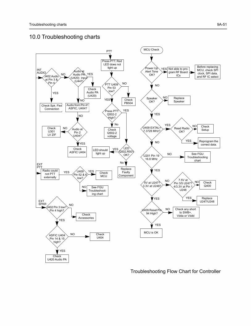
Troubleshooting charts 9A-51
10.0 Troubleshooting charts
MCU Check
Power Up Alert Tone
OK?
SpeakerOK?
U409 EXTAL= 7.3728 MHz?
U201 Pin 19 16.8 MHz
5V at U247?3.3V at U248?
U409 Reset Pin 94 High?
MCU is OK
Not able to pro-gram RF Board
ICs
Before replacing MCU, check SPI clock, SPI data, and RF IC select
Replace Speaker
Read Radio OK?
Check Setup
Reprogram the correct data.
See FGU Troubleshooting
chart
7.5V at Pin 3/5 U247? 4/3.3V at Pin 1
U248
Check Q400
Replace U247/U248
Check any short to SWB+,
Vdda or Vddd
Press PTT. Red LED does not
light up
PTT U409 Pin 53 low?
Press PTT Q502-2 High?
Check PB504
Check Q502-2 voltage
LED Q502,R501
OK?
Replace Faulty
Component
Radio could not PTT
externally
U409 Pin 52 & 6
low?
See FGU Troubleshoot-
ing chart
LED should light up
Check MCU
PTT
NO
YES
YES
No
No
YES YES
NO
YES
YES
NO
NO
YES
YES
NO
NO
YES
NO
YES
NO
YES
YES
NO
NO
YES
EXTSPKR
EXTPTT
INTAUDIO
J402 Pin 3 low? Pin 4 high?
ASFIC U404 Pin 14 & 15
high?
Check Accessories
Check U404
Check U420 Audio PA
NO
NO
YES
YES
J402 Audio at Pin 3 &
Pin 4
Check Spk. Flex Connection
Audio at Audio PA
(U420) input (U447)
Audio from Pin 41 ASFIC, U404?
Check ASFIC U404
Check Audio PA
(U420)
Check U301
LV ZIF
Audio at Pin 2
U404?
NO
NO
NO
YES
YES
NO
YES
Troubleshooting Flow Chart for Controller

9A-52 Troubleshooting charts
Bad SINADBad 20dB Quieting
No Recovered Audio
START
Audio at pin 27 of U301? Check Controller
Yes
No
Spray of inject 1st IF into XTAL Filter
IF Freq: 45.1MHz
Audio heard?BYes
No
Check 2nd LO Control Voltage at C363
VCO locked?BYes
16.8 MHz check at pin 22 U301?
Activity on U301
LVZIF_SEL pin?
Check FGU
No
No
A
A
Yes
Check Q320 bias circuitry for faults.
Rotate Freq. Knob
Check controller
Before replacing U301, check 2nd VCO Q320. Check VCO O/P level,
C351, C352.
Yes
No
Troubleshooting Flow Chart for Receiver (Sheet 1 of 2)

Troubleshooting charts 9A-53
IF Signal at L311?
No
RF Signal at T301?
RF Signal at C310?
No
RF Signal at C307?
No
RF Signal at C301?
No or
Check harmonic filters L101 & L102 and ant. switches CR101, CR102, L104
Check filter between C301 & C307; program filter to schematic test
freq and check varactor voltages.
Inject RF into J101
Are varactor voltages OK?
No
Yes
Check RF amp (Q301) Stage.
Check filter between C310 & T301.
Yes
Check T301, T302, CR306, R308, R309,
R310Yes
1st LO O/P OK?
Locked?
Yes
Check FGU
Yes
Trace IF signal from L311 to
Q302. Check for bad XTAL filter.
No
Yes Q302 collec-tor OK?IF signal present?
Before replacing U301, check
U301 voltages; trace IF signal
path.
Yes
Check for 2.6 VDC
Is R5 present?
Check Q210, U201 (pin 48) voltages and
U247
No
No
No
Check U404 voltage. U404 can be selected by
MCU before replacing U404.
Check varactor filter.
No
Yes
Yes
Yes
A
A
B
weak RF
Troubleshooting Flow Chart for Receiver (Sheet 2 of 2)

9A-54 Troubleshooting charts
START
No Power
Is There B+ Bias for Ant switch
CR101
Check Q111
Is Current OK?
Is Control Voltage High or Low at
C119
Check PCIC
1. Check Pin Diodes2. Check Harmonic Filter
Inspect/Repair Tx. Output Network
Is Power OK?
Done
Check Drive to Module
Is Drive OK? Troubleshoot
VCO
Inspect PA Network/Check Power Out of U101 at Cap C160
Is Power OK?
Replace U101
Is Power OK?
Replace Q110
Done
Done
No
Yes
Yes No
No
Yes
Low
High
No
Yes
Yes
No
Yes
No
Troubleshooting Flow Chart for Transmitter

Troubleshooting charts 9A-55
5V at pin 6 of
CR201
Is informationfrom µP U409
correct?
Is U201 Pin 18AT 4.54 VDC?
Is U201 Pin 47 13 VDC
Is U241 Pin 19<0.7 VDC in RX &>4.3 VDC in TX?
Start
Visual check of the Board OK?
CorrectProblem
Check 5VRegulator
+5V at U201Pin’s
13 & 30?
Is 16.8MHzSignal at
U201 Pin 19?
Check FL201, C206, C207, C208, CR203 &
R204
Are signalsat Pin’s 14 &15 of U201?
Check L202 Check Q260,
Q261 & R260
U201 pin 2 at >3V in Tx and <0.7V in Rx
Replace U201
RemoveShorts
Is there a shortbetween Pin 47 and
Pins 14 & 15 ofU201?
Replace orresolder
necessarycomponents
Is RF level atU201 Pin 32 >-30 dBm?
Are R231,R232,R233,C231,C232,
& C233 OK?
Replace U201
If L261, C263 & C264are OK, then see VCOtroubleshooting chart
Are Waveformsat Pins 14 & 15
triangular?
Do Pins 7,8 & 9of U201 togglewhen channel is
changed?
Check programminglines between U409
and U201 Pins 7,8 & 9
Replace U201
Check uP U409Troubleshooting
Chart
NO
YES
NO
YES
NO
YES
NO
YES
NO
NO
NO
YES
YES
NO
YES
YES
NO
YES
YES
YESNO
NO
NO
NO
YES
NO
YES
YES
Check CR201, U210, U211, C258, C259 &
C228
3.3V at U201 pins 5, 20, 34 &
36
Check U248, L201 & L202
Is 16.8MHz signal at U201 pin
23?
Replace U201
YES
NO
NO
YES
NO
YES
Troubleshooting Flow Chart for Synthesizer

9A-56 Troubleshooting charts
START
No LO?
Tx Carrier?
VCO OK
Check R260
TRB = 5V? @U241
Pin 19
U241 Pin 10 >1V?
L253 O/C? Change L253
Change U241
AUX 3 High?
Check U201 Pin 2 for 3.2V
U241 Pin 19 =0V
AUX 4 High?
Change Q261
VCTRL 0V or 13V? L243 Open
Circuit?
Change U241
Change L243
Change U201
Check for faulty parts or dry joints of L271, L273, C370,
C386, R339 & L309
A
A
No
No
Yes
Yes
Yes
No
No
Yes
Yes
Yes
No
Yes
No
No
Yes
Yes
No
No
Check R245 for dry joint or faulty
No
Troubleshooting Flow Chart for VCO

9B-1
Section 9B
MODEL CHART AND TEST SPECIFICATIONS (136-174 MHZ)
1.0 Model Chart
GP88s , VHF, 136-174 MHzModel Description
AZH34KDC9AA3 GP88s 136-174 MHz 5W 16 CH
Item Description
X PMUD1590* GP88s Super Tanapa 136-174 MHz 5W
X PMUD1591* GP88s Tanapa 136-174 MHz 5W
X PMLD4162 GP88s B/C Kit 136-174 MHz 5W
X PMLN4343 GP88s Front Housing Kit
X PMAD4012 Antenna, 136-155 MHz Stubby
X PMAD4013 Antenna, 155-174 MHz Stubby
X PMAD4014 Antenna, 136-155 MHz 14 cm
X PMAD4015 Antenna, 155-174 MHz 14 cm
X PMAD4023 Antenna, 150-161 MHz 14 cm
X PMAD4025 Antenna, 150-161 MHz Stubby
X 6804111J46 GP88s User Guide
x = Indicates one of each is required.* Motorola Depot Servicing only

9B-2 Specifications
2.0 Specifications
General
Transmitter
Receiver
All specifications are subject to change without notice.
VHF
Frequency: 136-174 MHz
Channel Capacity: GP88s : 16 Channels
Power Supply: 7.5 Volts ±20%
Dimensions with Standard High Capacity NiMH Battery:
57.5mm x 134mm x 38mm
Weight: with Standard High Capacity NiMH Battery: with High Capaci-ty NiCd Battery:
429 g
454 g
Average Battery Life @ (5-5-90 Duty Cycle) Standard High Capacity NiMH Bat-tery:
Low Pow-er
10 hrs
High Pow-er
8 hrs
Sealing: Passes rain testing per IP54
Shock: Meets MIL-STD-810-C,D & E and TIA/EIA 603
Vibration: Meets MIL-STD-810-C,D & E and TIA/EIA 603
Dust: Meets MIL-STD-810-C,D & E and IP54
Humidity: Meets MIL-STD-810-C,D & E and TIA/EIA 603
VHF
RF OutputNiMH @ 7.5V:
Low1W
High5W
Frequency 136-174 MHz
Channel Spacing 12.5/20/25 kHz
Freq. Stability(-30°C to +60°C)
0.00025%
Spurs/Harmonics: -36 dBm < 1 GHz-30 dBm > 1 GHz
Audio Response:(from 6 dB/oct. Pre-Emphasis, 300 to 3000Hz)
+1, -3 dB
Audio Distortion:@ 1000 Hz, 60%Rated Max. Dev.
<5%
FM Noise: -40 dB
VHF 12.5kHz
VHF 20/25kHz
Frequency: 136-174MHz
136-174MHz
Sensitivity12dB EIA SINAD:
0.35 µV 0.35 µV
Adjacent Channel Selectivity ETS
-60 dB -70 dB
Intermodulation ETS
-65 dB -65 dB
Freq. Stability(-30°C to +60°C):
0.00025% 0.00025%
Spur Rejection: -70 dB -70 dB
Image Rejection: -70 dB -70 dB
Audio Output@ <5% Distortion
500 mW 500 mW

Transmitter 9B-3
3.0 Transmitter
3.1 General(Refer to Figure 9-1)
The VHF transmitter contains five basic circuits:
1. power amplifier
2. antenna switch
3. harmonic filter
4. antenna matching network
5. power control integrated circuit (PCIC).
3.1.1 Power Amplifier
The power amplifier consists of two devices:
1. 9Z67 LDMOS driver IC (U3501) and
2. PRF1507 LDMOS PA (Q3501).
The 9Z67 LDMOS driver IC contains a 2 stage amplification with a supply voltage of 7.3V.
This RF power amplifier is capable of supplying an output power of 0.3W (pin 6 and 7) with an input signal of 2mW (3dBm) (pin16). The current drain would typically be 130mA while operating in the frequency range of 136-174MHz.
The PRF1507 LDMOS PA is capable of supplying an output power of 7W with an input signal of 0.3W. The current drain would typically be 1800mA while operating in the frequency range of 136-174MHz. The power output can be varied by changing the biasing voltage.
Figure 9-1 Transmitter Block Diagram
PCIC
Antenna
PA Antenna Switch/
Driver Harmonic Filter/
Vcontrol Vcontrol
From VCO
Jack
PA-FinalStage Matching Network

9B-4 Transmitter
3.1.2 Antenna Switch
The antenna switch circuit consists of two PIN diodes (D3521 and D3551), a pi network (C3531, L3551 and C3550), and two current limiting resistors (R3571, R3572, R3573 ). In the transmit mode, B+ at PCIC (U3502) pin 23 will go low and turn on Q3561 where a B+ bias is applied to the antenna switch circuit to bias the diodes "on". The shunt diode (D3551) shorts out the receiver port, and the pi network, which operates as a quarter wave transmission line, transforms the low impedance of the shunt diode to a high impedance at the input of the harmonic filter. In the receive mode, the diodes are both off, and hence, there exists a low attenuation path between the antenna and receiver ports.
3.1.3 Harmonic Filter
The harmonic filter consists of C3532 to C3536, L3531 and L3532. This network forms a low-pass filter to attenuate harmonic energy of the transmitter to specifications level. The harmonic filter insertion loss should be less than 1.2dB.
3.1.4 Antenna Matching Network
A matching network which is made up of L3538, C3537 and C3539 is used to match the antenna's impedance to the harmonic filter. This will optimize the performance of the transmitter and receiver into an antenna.
3.1.5 Power Control Integrated Circuit (PCIC)
The transmitter uses the Power Control IC (PCIC), U3502 to control the power output of the radio by maintaining the radio current drain. The current to the final stage of the power module is supplied through R3519 (0.1ohms), which provides a voltage proportional to the current drain. This voltage is then fedback to the Automatic Level Control (ALC) within the PCIC to keep the whole loop stable.
The PCIC has internal digital to analog converters (DACs) which provide the reference voltage of the control loop. The voltage level is controlled by the microprocessor through the data line of the PCIC.
There are resistors and integrators within the PCIC, and external capacitors (C3562, C3563 and C3565) in controlling the transmitter rising and falling time. These are necessary in reducing the power splatter into adjacent channels.
U3503 and its associated circuitry acts as a temperature cut back circuitry. This circuitry provides the necessary voltage to the PCIC to cut the transmitter power when the radio temperature gets too high.

Receiver 9B-5
4.0 Receiver
4.1 Receiver Front-End(Refer toVHF Receiver Front End Schematic Diagram on page 9B-16, VHF Receiver Back End Schematic Diagram on page 9B-17, and VHF Transmitter Schematic Diagram on page 9B-20)
The RF signal is received by the antenna and applied to a low-pass filter. For VHF, the filter consists of L3531, L3532, C3532 to C3536. The filtered RF signal is passed through the antenna switch. The antenna switch circuit consists of two PIN diodes(D3521 and D3551) and a pi network (C3531, L3551 and C3550).The signal is then applied to a varactor tuned bandpass filter. The VHF bandpass filter comprises of L3301, L3303, C3301 to C3304 and D3301. The bandpass filter is tuned by applying a control voltage to the varactor diode (D3301) in the filter.
The bandpass filter is electronically tuned by the DACRx from U404 which is controlled by the microprocessor. Depending on the carrier frequency, the DACRx will supply the tuned voltage to the varactor diodes in the filter. Wideband operation of the filter is achieved by shifting the bandpass filter across the band.
The output of the bandpass filter is coupled to the RF amplifier transistor Q3302 via C3306. After being amplified by the RF amplifier, the RF signal is further filtered by a second varactor tuned bandpass filter, consisting of L3305, L3306, C3311 to C3314 and D3302.
Both the pre and post-RF amplifier varactor tuned filters have similar responses. The 3 dB bandwidth of the filter is about 12 MHz. This enables the filters to be electronically controlled by using a single control voltage which is DACRx .
Figure 9-2 VHF Receiver Block Diagram
Demodulator
Synthesizer
Crystal Filter
MixerVaractor Tuned Filter
RF AmpVaractor Tuned Filter
Pin Diode Antenna SwitchRF Jack
Antenna
AGC
Control Voltagefrom ASFIC
First LOfrom FGU
Recovered AudioSquelch
RSSI
IF IC
SPI Bus
16.8 MHzReference Clock
SecondLO VCO
IF Amp
U3220

9B-6 Receiver
The output of the post-RF amplifier filter is connected to the passive double balanced mixer which consists of T3301, T3302 and CR3301. Matching of the filter to the mixer is provided by C3317, C3318 and L3308. After mixing with the first LO signal from the voltage controlled oscillator (VCO) using high side injection, the RF signal is down-converted to the 45.1 MHz IF signal.
The IF signal coming out of the mixer is transfered to the crystal filter (Y3200) through a resistor pad (R3321 - R3323) and a diplexer (C3320 and L3309). Matching to the input of the crystal filter is provided by C3200 and L3200. The crystal filter provides the necessary selectivity and intermodulation protection.
4.2 Receiver Back-End(Refer to VHF Receiver Back End Schematic Diagram on page 9B-17)
The output of crystal filter Y3200 is matched to the input of IF amplifier transistor Q3200 by capacitor C3203. Voltage supply to the IF amplifier is taken from the receive 5 volts (R5). The gain controlled IF amplifer provides a maximum gain of about 10dB. The amplified IF signal is then coupled into U3220(pin 3) via L3202, C3207, and C3230 which provides the matching for the IF amplifier and U3220.
The IF signal applied to pin 3 of U3220 is amplified, down-converted, filtered, and demodulated, to produce the recovered audio at pin 27 of U3220. This IF IC is electronically programmable, and the amount of filtering (which is dependent on the radio channel spacing) is controlled by the microprocessor. Additional filtering, once externally provided by the conventional ceramic filters, is replaced by internal filters in the IF module (U3220).
The IF IC uses a type of direct conversion process, whereby the externally generated second LO frequency is divided by two in U3220 so that it is very close to the first IF frequency. The IF IC (U3220) synthesizes the second LO and phase-locks the VCO to track the first IF frequency. The second LO is designed to oscillate at twice the first IF frequency because of the divide-by-two function in the IF IC.
In the absence of an IF signal, the VCO will “search” for a frequency, or its frequency will vary close to twice the IF frequency. When an IF signal is received, the VCO will lock onto the IF signal. The second LO/VCO is a Colpitts oscillator built around transistor Q3270. The VCO has a varactor diode, D3270, to adjust the VCO frequency. The control signal for the varactor is derived from a loop filter consisting of C3278 to C3280, R3274 and R3275.
The IF IC (U3220) also performs several other functions. It provides a received signal-strength indicator (RSSI) and a squelch output. The RSSI is a dc voltage monitored by the microprocessor, and used as a peak indicator during the bench tuning of the receiver front-end varactor filter. The RSSI voltage is also used to control the automatic gain control (AGC) circuit at the front-end.
The demodulated signal on pin 27 of U3220 is also used for squelch control. The signal is routed to U404 (ASFIC) where squelch signal shaping and detection takes place. The demodulated audio signal is also routed to U404 for processing before going to the audio amplifier for amplification.

Receiver 9B-7
4.3 Automatic Gain Control Circuit(Refer to VHF Receiver Front End Schematic Diagram on page 9B-16 and VHF Receiver Back End Schematic Diagram on page 9B-17)
The front end automatic gain control circuit provides automatic reduction of gain, of the front end RF amplifier via feedback. This action is necessary to prevent overloading of backend circuits. This is achieved by drawing some of the output power from the RF amplifier output. At high radio frequencies, capacitor C3327 provides the low impedance path to ground for this purpose. CR3302 is a PIN diode used for switching the path on or off. A certain amount of forward biasing current is needed to turn the PIN diode on. Transistor Q3301 provides this current.
Radio signal strength indicator, RSSI, a voltage signal, is used to drive Q3301 to saturation i.e. turned on. RSSI is produced by U3220 and is proportional to the gain of the RF amplifier and the input power to the radio.
Resistors R3304 and R3305 are voltage dividers designed to turn on Q3301 at certain RSSI levels. In order to turn on Q3301 the voltage across R3305 must be greater or equal to the voltage across R3324 + Vbe. Capacitor C3209 is used to dampen any instability while the AGC is turning on. The current flowing into the collector of Q3301, a high current gain NPN transistor, will be drawn through the PIN diode to turn it on. Maximum current flowing through the PIN is limited by the resistors R3316, R3313, R3306 and R3324. C3326 is a feedback capacitor used to provide some stability to this high gain stage.
An additional gain control circuit is formed by Q3201 and its associated circuitry. Resistors R3206 and R3207 are voltage dividers designed to turn on Q3201 at a significantly higher RSSI level than the level required to turn on PIN diode control transistor Q3301. In order to turn on Q3201 the voltage across R3207 must be greater or equal to the voltage across R3208, plus the base-emitter voltage (Vbe) present at Q3201. As current starts flowing into the collector of Q3201, it reduces the bias voltage at the base of IF amplifier transistor Q3200 and in turn, the gain of the IF amplifier. The gain can be controlled in a range of -30dB up to +10dB.

9B-8 Frequency Generation Circuitry
5.0 Frequency Generation Circuitry
The Frequency Generation Circuitry is composed of two main ICs, the Fractional-N synthesizer (U3701), and the VCO/Buffer IC (U3801). Designed in conjunction to maximize compatibility, the two ICs provide many of the functions that normally would require additional circuitry. The synthesizer block diagram illustrates the interconnect and support circuitry used in the region. Refer to the relevant schematics for the reference designators.
The synthesizer is powered by regulated 5V and 3.3V which come from U3711 and U3201 respectively. The synthesizer in turn generates a superfiltered 4.5V which powers U3801.
In addition to the VCO, the synthesizer must interface with the logic and ASFIC circuitry. Programming for the synthesizer is accomplished through the data , clock and chip select lines from the microprocessor. A 3.3V dc signal from synthesizer lock detect line indicates to the microprocessor that the synthesizer is locked.
Transmit modulation from the ASFIC is supplied to pin10 of U3701. Internally the audio is digitized by the Fractional-N and applied to the loop divider to provide the low-port modulation. The audio runs through an internal attenuator for modulation balancing purposes before going out to the VCO.
Figure 9-3 Frequency Generation Unit Block Diagram
Voltage Multiplier
Synthesizer U3701 Loop
Filter
VCOBIC U3801
ToMixer
ToPA Driver
VCP
Vmult1Aux3
MOD OutModulatingSignal
Vmult2
Rx VCO Circuit
Tx VCO
TRB
16.8 MHzRef. Osc.
Rx Out
Tx Out
Circuit

Frequency Generation Circuitry 9B-9
5.1 Synthesizer(Refer toVHF Synthesizer Schematic Diagram on page 9B-18)
The Fractional-N Synthesizer uses a 16.8MHz crystal (Y3761) to provide a reference for the system. The LVFractN IC (U3701) further divides this to 2.1MHz, 2.225MHz, and 2.4MHz as reference frequencies. Together with C3761, C3762, C3763, R3761 and D3761 , they build up the reference oscillator which is capable of 2.5ppm stability over temperatures of -30 to 85°C. It also provides 16.8MHz at pin 19 of U3701 to be used by ASFIC and LVZIF.
The loop filter which consist of C3721, C3722, R3721, R3722 and R3723 provides the necessary dc steering voltage for the VCO and determines the amount of noise and spur passing through .
In achieving fast locking for the synthesizer, an internal adapt charge pump provides higher current at pin 45 of U3701 to put synthesizer within the lock range. The required frequency is then locked by normal mode charge pump at pin 43 .
Both the normal and adapt charge pumps get their supply from the capacitive voltage multiplier which is made up of C3701 to C3704 and triple diodes D3701, D3702. Two 3.3V square waves ( 180 deg out of phase) are first multiplied by four and then shifted, along with regulated 5V, to build up 13.5V at pin 47 of U3701.
Figure 9-4 Synthesizer Block Diagram
DATA
CLK
CEX
MODIN
VCC, DC5V
XTAL1
XTAL2
WARP
PREIN
VCP
REFERENCEOSCILLATOR
VOLTAGEMULTIPLIER
VOLTAGECONTROLLED OSCILLATOR
2-POLELOOPFILTER
DATA (U409 PIN 100)
CLOCK (U409 PIN 1)
CSX (U409 PIN 2)
MOD IN (U404 PIN 40)
+5V (U3711 PIN 4)
7
8
9
10
13, 30
23
24
25
32
47
VMULT2 VMULT1
BIAS1
SFOUT
AUX3
AUX4
IADAPTIOUT
GND
FREFOUT
LOCK 4
19
6, 22, 23, 24
4345
3
2
28
14 15
40
FILTERED 5V
STEERINGLINE
LOCK (U409 PIN 56)
PRESCALER IN
LO RF INJECTION
TX RF INJECTION(1ST STAGE OF PA)
FREF (U3220 PIN 21 & U404 PIN 34)
39BIAS2
41
DUAL TSTRS
48
5VR5
5, 20, 34, 36(U3201 PIN 5)
AUX1
VDD, 3.3V MODOUT
U3701 LOW VOLTAGE FRACTIONAL-N SYNTHESIZER

9B-10 Frequency Generation Circuitry
5.2 VCO - Voltage Controlled Oscillator(Refer toVHF Voltage Controlled Oscillator Schematic Diagram on page 9B-19)
The VCOBIC (U3801) in conjunction with the Fractional-N synthesizer (U3701) generates RF in both the receive and the transmit modes of operation. The TRB line (U3801 pin 19) determines which oscillator and buffer will be enabled. A sample of the RF signal from the enabled oscillator is routed from U3801 pin 12, through a low pass filter, to the prescaler input (U3701 pin 32). After frequency comparison in the synthesizer, a resultant CONTROL VOLTAGE is received at the VCO. This voltage is a DC voltage typically between 3.5V and 9.5V when the PLL is locked on frequency.
Figure 9-5 VCO Block Diagram
Presc
RX
TX
MatchingNetwork
Low Pass Filter
Attenuator
Pin8
Pin14
Pin10
(3701 Pin28)
VCC Buffers
TX RF Injection
U3701 Pin 32
AUX3 (U3701 Pin2)
Prescaler Out
Pin 12Pin 19Pin 20
TX/RX/BSSwitching Network
U3801VCOBIC
RxActive Bias
TxActive Bias
Pin2
Rx-I adjust
Pin1
Tx-I adjust
Pins 9,11,17Pin18
VsensCircuit
Pin15
Pin16
RX VCO Circuit
TX VCO Circuit
RX Tank
TX Tank
Pin7
Vcc-Superfilter
Collector/RF in
Pin4
Pin5
Pin6
RX
TX
(U3701 Pin28)
Rx-SW
Tx-SW
Vcc-Logic
(U3701 Pin28)
Steer Line Voltage (VCTRL)
Pin13
Pin3
TRB_IN
LO RF INJECTION
VSF
VSF
VSF

Frequency Generation Circuitry 9B-11
The RF section of the VCOBIC(U3801) is operated at 4.54 V (VSF), while the control section of the VCOBIC and Fractional-N synthesizer (U3701) is operated at 3.3V. The operation logic is shown in Table 9-1.
In the receive mode, U3801 pin 19 is low or grounded. This activates the receive VCO by enabling the receive oscillator and the receive buffer of U3801. The RF signal at U3801 pin 8 is run through a matching network. The resulting RF signal is the LO RF INJECTION and it is applied to the mixer at T3302.
During the transmit condition, when PTT is depressed, 3.2 volts is applied to U3801 pin 19. This activates the transmit VCO by enabling the transmit oscillator and the transmit buffer of U3801. The RF signal at U3801 pin 10 is injected into the input of the PA module (U3501 pin16). This RF signal is the TX RF INJECTION. Also in transmit mode, the audio signal to be frequency modulated onto the carrier is received through U3701 pin 41.
When a high impedance is applied to U3801 pin19, the VCO is operating in BATTERY SAVER mode. In this case, both the receive and transmit oscillators as well as the receive transmit and prescaler buffer are turned off.
Table 9-1 VCO Control Logic
Desired Mode
AUX 4 AUX 3 TRB
Tx n.u. High (@3.2V) High (@3.2V)
Rx n.u. Low Low
Battery Saver n.u. Hi-Z/Float (@1.6V)
Hi-Z/Float (@1.6V)

9B-12 Notes For All Schematics and Circuit Boards
6.0 Notes For All Schematics and Circuit Boards* Component is frequency sensitive. Refer to the Electrical Parts List for value and usage.
1. Unless otherwise stated, resistances are in Ohms (k = 1000), and capacitances are in picofarads (pF) or microfarads (µF).
2. DC voltages are measured from point indicated to chassis ground using a Motorola DC multime-ter or equivalent. Transmitter measurements should be made with a 1.2 µH choke in series with the voltage probe to prevent circuit loading.
3. Reference Designators are assigned in the following manner:
400/500 Series = Controller
600 Series = Keypad Board
3200 Series = IF Circuitry
3300 Series = Receiver
3500 Series = Transmitter
3700 and 3800 Series = Frequency Generation
4. Interconnect Tie Point Legend:
UNSWB+ = Unswitch Battery Voltage (7.5V)
SWB+ = Switch Battery Voltage (7.5V)
R5 = Receiver Five Volts
CLK = Clock
Vdda = Regulated 3.3 Volts (for analog)
Vddd = Regulated 3.3 Volts (for digital)
CSX = Chip Select Line (not for LVZIF)
SYN = Synthesizer
DACRX = Digital to Analog Voltage (For Receiver Front End Filter)
VSF = Voltage Super Filtered (5 volts)
VR = Voltage Regulator
6-LAYER CIRCUIT BOARD DETAIL VIEWINGCOPPER STEPS IN PROPER LAYER SEQUENCE
LAYER 1 (L1)
LAYER 2 (L2)LAYER 3 (L3)
LAYER 4 (L4)
LAYER 5 (L5)LAYER 6 (L6)
INNER LAYERS
SIDE 1
SIDE 2

9B
-13
C3518
R35
12
R35
44R
3546
R35
47
R3548
SH3502
C35
19
C35
27
L3518
L352
2
R35
13
L3521
12 3
Q35
01
C3514
17
C35
21
C35
23L3515
21
22
23
643
T33
01
C3318
C33
19
C33
29 C3330
C33
31
C33
32
L3306
R33
17
C33
10C3311C3312C3313
C33
14
C3327D3302
L3305
C33
06
C33
07C
3338
CR
3303
Q3302
R33
08R
3309
R33
10
R3311R3312
R3313SH3303
C33
08
C33
09
L3304
R3316
C32
06
L3202
Q32
00
04
C32
04C
3207
C32
08
C3210
Q32
01
R3201
R3202
R32
06
R3209
R32
10
R3212
PB504
C3212
R32
14 R32
15
R3217
U32
01C
3209
C3214
C32
15Q
3202
R3213
R32
18
R3225
C32
25
C3270
C32
72
C32
73
C32
74C
3275
C32
76
C3278
C3279
Q3270
R3226
R32
70
R32
71
R32
72
R32
73
R3274
SH3201
C32
71
C3277
C32
80
D32
70
L327
0
L327
1
R3275
R32
76
C3213
PB502
C50
2
C52
1
PB501
VR440
C50
5
C50
6C
507
Q505
R50
5
R50
6
R50
7
VR501
C513
4 3
2CR503 Q502R
501
R50
2
C512
C51
1
C51
4
L3538
C477
C47
8 C50
1C
504
C50
8
C509
C3537
C3539
4
2
J407
43
2
J404
C454
C49
9C
518
C520
VR432
VR
433
C498C519
ZMY0130325-A
VHF (136-174MHz) Main Board Top Side PCB No. 8480675Z01
Circuit Board/Schematic Diagrams and Parts List
7.0 Circuit Board/Schematic Diagrams and Parts List
1
J400
40
TP401
Q431
R49
3 R49
4
R49
9
RT400TP402TP410
R49
8
C47
0
C471
C472
C483C484
C48
5
CR
413
2
1
3
4
6
5
J402
4 3
Q41
7Q
433
TP405TP406 TP415
C40
1CR412
R401
R40
2
R405
R427
R476
SH401
4
5 8U400
C40
0
C402
C403
Q40
0
R40
3
R40
6
C467
CR
440
Q403
R44
6R
447
R44
8
R481
C48
0
C48
2
43
Q405 R41
6
C424
C429
R408
R428
R42
9
R478
R49
2
SH400
C427 C428
145
8
U40
7
C425C426
2271
218
U405C
423 R410
R41
8
R437 32 17
U40
616
1
C529C531
3
Y3761
C43
2
TP3702
C3712 C37
13C3715
C3716
C3741
C3742
R3701
R3741
C3706
C3714
C3743
C3744
C3746
C37
53
C37
21
C3722
C37
52
C37
54
43
Q3721
R3721
R3722
R37
51 R3752
SH3701
C3710
C37
24
R3723
C37
11
C3745
U37
11
C3832C3833
C38
42
D38
32
L3834 R3833 R3834
R38
35
R38
36
C3834
C38
35
C3836
D3831 L3831
L383
2
L383
3
L382
2
L382
3L3825
SH3801
C38
22
C3824C3825
C38
26
C3830
D3821 L3821
R38
21R3822
R38
23C
3828
C38
29
L3824
R38
28
C3501
C3503
C3504C3505 L3
503
R3501
R3502
R3503
R35
05
1
16
8
9
U3501
C3502
C35
41
C35
42
C35
43
C35
44
L3501
R35
41
R35
42R35
43
R35
45C
3546
C35
47
C35
L350
2
L3511
L351
2
L3513C3512
C3513
L3504
C33
20
C3334
C33
35
L3312
R3318
TP3301 L3309 R33
R33
R33
SH3302
64 3
T33
02
C52
3C
524
C52
5
C52
6 4 3
Q50
6V
R43
1
VR
450V
R45
1
C44
6
C45
5C
515
C527C528
C53
0R
510
TP3701
C51
6
C517
C3205 R3200 VR
444
C3203
R32
03R
3207
R32
08Y3200
C3200C3201
C32
02L3200
L320
1
R32
11
SH3203
R32
R32
05

Circuit Board/Schematic Diagrams and Parts List
C52
2
C3751
C3763D3761
R3760R3761
2
3
4
Y3762
C3701C3702
C3703
C37
07C3731
C37
32
C37
61
R3703
R3704R37
62
SH3702
137
25 13
U3701C3705
C3708
C3725 C37
33
C37
34
L373
1
R3702
R37
05
R3726
C3704
C37
09
D3701
D37
02
C38
12
C38
13
C3818
R3812
R38
18
R38
26
11
1 20
10
U3801
C3803
5
C38
06
C38
10
C38
21
C38
23
L3812
826
R3803
804
805
R38
06R
3808
R38
11
R38
24R
3825
SH3802
C3815
C38
16
C3827
L3813
L381
6
R3816
R38
17
R38
29
R38
30
R3831
R3832C408C409C410C412
C443
C414
C41
5 C430
C451
C45
2
SH403
C411
1
37 25
13
U404
C450
43
Q410
C476
R471
11
1
20
10
U420
C41
6C
422
C442
C447
R400
R423
R472R473 C475
C40
7 C41
9 C42
0C421C479
C481C487
R413
R42
5
R445
R449R475
C431C433
C434
C435
C494
43
Q418
Q41
9
R414R415
R419
R460
R461
R462
U41
0
C44
9C
463
E4001
76
U409
C45
3
C45
6
C49
3 L410
L411
R411
R43
2
R457
C48
6
C48
8
5126
SH402
CR414
R463
C489
C440
C458C459
C466C473L4
00
Q42
0
Q421
R434
R435
R43
6R438
R439
R467
R495
R496
ZMY0130324-A
9B-14
4
53
2S502
4
C
8
C
2
1
S501
2
3
4
1
J3501
J3502
C3533
L3531
L3532
C3531C3532
C3550
C3551
C3552L3552 R3551
SH3501
C3524
C3525
C35
28C35
34
C3535
C3536
C3301
C3302
C3303C3304
C3305
C33
21
C3322 C3323
C33
24
D3301
L3301 L3303
R3303
C3325
C3326
CR3302
Q33
01
R3304R3305
R3306R3307
R33
14
R33
15
R3324
SH3301
C33
15
C33
16 C3339
C33
17 C3337
CR3301
L330
8
R3319R3320
C32
11C
3218
C32
20
C3221
C32
22
C3227
C32
28
C3230
C32
38
C3243
C3244
L3221
R32
20
R32
21
R3222
C3219C3223R3219
137
25 13
U3220
C32
26
C32
29C3239
SH3202
C3241
C32
24
C32
31
C32
32
C32
33
C32
34
C3235
C3236
C3237
C3240
C32
42
R3223
R32241
2
3
B501
CR501
L505
R3763
VR
439
VR441VR506
C50
0
C3735
C37
62L3
701
C37
55
C3726
C37
27
R37
27
C503
C3336
F50
1
C3526 C3569L3523
R3571R3572R3573 TP3502
H3501
C3516
D3521
D3551
L3551
C3506
C3507 C3509
C3561
C3566
C3567
L3519
R3561
R35
62
R35
63
U35
03
C3560 C3568
C35
70
1
179
25
U3502
C3562
C3563
C3565
R3564
R3565
C3515
C35
64
R3519C3508
Q35
61R
3570
R35
69
C3801
C3802
C3804
C380
C3808
C38
09
C38
11
L380
1L3
809 L3
811
L3
Q38
01
R3801
R38
02
R3
R3
R38
07
VHF (136-174MHz) Main Board Bottom Side PCB No. 8480675Z01

9B
-15
10.0VVR450
10.0VVR451
1S1
4S2
2S3
J407
SPN
SPP
IC
0.1uFC515
Q503
2
6
4
1
3
4.7K47K
47K
10K
10KR510
C478100pF
100pFC477
VR4316.8V
SCI
100pFC498
100pFC499
4700pFC446
C454100pF C455
470pFC5201000pF
C5181000pF
C5191000pF
C5041000pF
C5011000pF
1S1
S23
4S3
2S4
J404
INT_MIC
INT_SPN
3
1
VR43310V22
3
1
10VVR432
C5091000pF
C508100pF
ZMY0130312-A
VHF Controls And Switches Schematic Diagram
Circuit Board/Schematic Diagrams and Parts List
0.47uFC502
MECH_SWB+
TAB1
TAB2
5
3
HIG
H
6
7
2
SWITCH
4
1
LOW
S502
0R507
Vdda
VOL
6.8VVR501 C505
100pF100pF
51
6
IMX1
24
3
SWB+
RED_LED
Q502R50510K
Q505 47KR506
Vdda
180R502
2 4
1 3CR503
R501680 RTA3
RTA2
RTA0RTA1
GREEN_LED
C514100pF100pF
C513100pF
C512100pFC511 7
GND GND19
1PC0
2PC1
4 PC2 PC38
S501SWITCH
C0 C0C1C1
CR501
24VF501
21
10VVR439
UNSWB+
1000pFC500
100pFC503
BATT_CODE
6.8VVR506
L505390nH
B501
RSSI_FIL2
NEG1
POS3
.01uFC521
2
6.8VVR440
SB1 1SWITCHPB501
6.8VVR444
2PTT
1
SWITCHPB504
.01uFC522
VR4416.8V
PB502
12SWITCH
SB2
ANT_BIAS
M
5V
C5071000pF
C506100pF
C5241000pF
C523100pF

Circuit Board/Schematic Diagrams and Parts List
NU1K
R3320
.022uF
C3318
1KR3319
NU
22pFC3335
150nH
L3309
R3321150
39pFC3317
0pF313
C33146.8pF
C3339
NU
10pF
82pF
C3320
SH3303SHIELDSHIELD
SH3302SHIELDSHIELD
SH3301SHIELDSHIELD
L3308
C3315
10nH06
10pF
H
33nHL3312
CR3301
2
34
1
C3319NU
C333420pF
IF
R3322
R3323220
18
C33163.3pF
2
IF_1_FE
XFMR
T3302
4
6
3
1
T3301
XFMR4
6
3
1
2
TP3301
470R3318
400mV w. RF Vltmtr-16dBm @50Ω
ZMY0130321-O
9B-16
CR3303
R3306
R3324
2.2K
220
R3311NU2.2pF
10
C3305
C3321
C3311
330pFC3324
150pF
33pF
Q3301
470nHL3304
20pFC3303
100K
R3317
10
R3314
R3316300
100K
R3303
C3308330pF
C3338
RX_IN_1_FE
470pF
C3307100pF
12nHL3303
15C3
RX_IN
R5
C3332
RX_INJ_1_FE
L3301
39pF
12nH
33KR3307
D3302
0.1uFC3309
100pFC3323
22
R3313 C3312
16pF
L3312n
.022uFC3337
R3309
C3304
5.6K
C3331
150pF
C3330100pF100pF
0.1uF
C3326
NU
1000pFC3325
330pFC3327
0.1uFC3306
330R3315
L330512nH
DACRx
C3322100pF
NUR3312
R5_2_FE R5_3_FE
R330133KNU
RSSI_1_FE
DACRx_1_FE
C3329330pF
C3301
RX_INJ
RSSI
5.6pF
C3310
NU1pF
100K
R3304
D3301
2.4KR3308
C3302
150pF
SMBV1032CR3302
Q3302
10K
R3310
UNSWB_PLUS_1_RX
UNSWB+
C333610uF
UNSWB_PLUS_2_RX
2.7V
R330568K RT3301
33KNU
0.7 - 5V136 - 174MHz
1.9V @ -47dBm at Ant. Conn0,3V @ no input at Ant. Conn
20mV
VHF Receiver Front End Schematic Diagram

9B
-17
C32411200pF
DA
TA
CLK
RSSI_OUT4
TE
ST
A16
TESTD8
VAG 32
VAG_REF 25
VPP9
PR
EA
MP
_OU
T47
PR
E_A
GC
48
PRE_IN3
RED_VCC1RED_VSS2
ROSE_VCC 30ROSE_VSS 29
RSSI_FLT5
GR
EE
N_V
CC
41
GR
EE
N_V
SS
43
15IO
UT
31LIM
42M
IX_B
YP
46M
IX_I
N
MLP
D_C
R24
PHASE_LOCK 26
DA
TA
DEMOD_HF 28DEMOD_OUT 27
EMIT11
EXTBS6
21F
RE
F
GN
D20
GOLD_VCC10
GO
LD_V
SS
14
39
C3M 35
C3P
38
C4M 36C4P
37
19C
EX
18C
LK
CO
L13 17
12
BLU
E_V
CC
45B
LUE
_VS
S44
BR
OW
N_V
CC
22 23B
RP
_OF
F
C1M 33
C1P
40
C2M 34
C2P
mgc_comps
U3220
AFC7
BASE
32D83
0.33uF
C3238
1uH
L3221
R3220
4.7K
.1uF3222
.01uFC3244
1uFC3234
1uFC3231
C32350.22uF
2.4KR3274
16_8MHz_3_ZIFC3278
0102726B13
SQ_OUT
0.1uF
1uFC3232
C328010nF
C3279
16.8
MH
z
2.2uF
C3226
SH3203SHIELD
0.1uF
SHIELD
C3237100pF
R3223
C3233
1K
1uF
.022uFC3239
SQ_OUT_1_ZIF
DATA_3_ZIF
CLK_3_ZIF
0.1uFC3225
10
R3224
0.22uFC3240
LVZIF_SEL_1_ZIF
DEMOD_1_ZIF
R32751K
C3229100pF
222NU
.01uFC3236
C3228.01uF
.01uF
LVZ
IF_S
EL
C3227
DEMOD
SHIELDSH3202SHIELD
10pF
C3220
C3242
0.1uF
C32230.1uF
0.1uFC3224
Vdd_FILTERED
Vdd_FILTERED
Vdd_FILTEREDVdd_FILTERED
VHF_ZIF
ZWG0130025-B
NU
NU
NU
1.5V
VHF Receiver Back End Schematic Diagram
Circuit Board/Schematic Diagrams and Parts List
R32051K
NU1µHL3201
L3200
Vdda
1µH
330pFC3271
1KR3209
4.7uFC3211
L32021uH
100pFC3203
R32124.7K
0C
IF
56pFC3275
39KR3207
5V_3_ZIF
RSSI
Q3201
R5_3_ZIF
12pFNU
C3202
R320410
R3276200K
82pFC3277
GN
D
1
GN
D1
2
GN
D2
3
GN
D3
4
OUT 3IN6
TBDXTALY3200
2.2pFC3207
D3270
100K
R3206
.01uFC3206
5V
C327433pF
4.7uFC3213
C32121uF
R3214
22
Q3200MMBR941R3203
R3221
10K
100
R3200
R5
150
47
SWB+
R3271
R32012.2K
C3204 C3205.01uF 0.1uF
C32080.1uF
NU
100R3208
C3201
NU1.5pF
2.2K
1uF
R3213
C3209
C3221.01uF
0.1uF
100
C3219
R3219
R3226
10
RSSI_1_ZIF
L32712.2uH
4.7KR3202
100KR3
C3243.022uF
1KR3270
C3273
10pF
47pFC3276
C3200
4.7uF
16pF
1ON_OFF
VIN
5VOUT
C3218
LP29801U3201
2
GND3
0R3215
Vdda_3_ZIF
R3218
SWB_PLUS_3_ZIF
2.2K
10
R3211
4.7pFC3272
IF_1_ZIF
R327247K
R327347K
Q3270 1
3
2
SHIELDSH3201
BFQ67W
SHIELD
C3230
100pF
RSSI_2_ZIF
.022uFC3270
L3270
Vdd_FILTERED5V
RSSI
100nH
RSSI
Vdd_FILTERED Vdd_FILTERED
5V
C3210 1000pF
10pFC3215
Q3202
VSF_3_ZIFVSF
5V
1K
R3225
0.1uFC3214
4V_3.3V
R32102,2k
NU
NU
2.9V
1.5V
1.9V @ -47dBm
4,5V
3,8V
1.5V
0.8V
3.3V

Circuit Board/Schematic Diagrams and Parts List
1234
UTUT
T
LT
SW
VR
OV
CP
PR
E_V
DD
PD
_VD
D
DV
DD
AV
DD
VBPASSPVREF
REFSEL
SFBASESFCAP
SFIN
MODIN
NC1NC2NC3
PREIN
DATA
BIAS1BIAS2
CCOMP
CEXCLK
PR
E_G
ND
PD
_GN
D
DG
ND
AG
ND
3344 622
1347 34 536 20
2135
18
2726
30
10
172931
32
7
4039
42
98
U370163A27
NROUT
3SDERR
1
GN
D
5IN
ADP3300U3711
SWB_PLUS_1_FN
2.2uFC3713
C37120.1uF
SWB+
35U
763U
GN
D3
OUT2
16.8MHz 45J49Y3761
D3761
R376147K
NUR3760
.01uFC3731C3763
2F
AD
J
4GND
3O
UT
1VDD
1.6pF
NU
OSC_16.8MHZ16.8MHz
Y3762
C3751NU
5V
C37332.2uF
2.2uHL3731
C3734.01uF.01uF
C3732
VddaVdda_1_FN
220pF220pFC3745C3742
220pFC3744 C3743
220pF
CSX_1_FN
DATA_1_FN
MODIN_1_FN
CLK_1_FN
CLK
MODIN
DATA
CSX
C3753C3752
4.7uF1000pF 0.1uF
C3754
VSF_1_FN
VSF
PRESC_1_FN
8.2pFC3726
PRESC
2.2uFC3755
200KR3751
R3752330K
R3727100K
100pFC3727
TP37021
ZMY0130322-A
9B-18
WARP
XTAL1XTAL2
TEST1TEST2
VMULTVMULTVMULTVMULT
SFOUT
MODOFREFO
IADAP
INDMU
IOUT
LOCK
AUX3AUX4
ADAPT
AUX1AUX2
25
2324
3738
15141211
28
4119
45
16
43
4
23
46
481
TRB_1_FN
LOCK
TRB
LOCK_1_FN
220pFC3746
BIAS_ADJ_1_FN
BIAS_ADJ
NUNU
C3725R3726
100R3701
2.2uFC3710
390nHL3701
0.1uFC3709R3703
150
C370722pF
NUR3702
C37080.1uF
33K
K11
K22
K33
R3705D3702
A16
A25
A34
R3704150
A2 5A3
4
1 K1
2 K2
3 K3
D3701
A16
C3703.01uF
C3704.01uF
.01uFC3701
.01uFC3702
0.1uFC3705
C37064.7uF
470R3721
100pFC3716
100pFC3715
4.7uFC3714
1uFC3724
R3723100
TP3701 1
0.1uFC3722
1KR3722
0.1uFC3721
4
1
3
Q3721
2
UMC5N
R5
5V
T5_1_FN
R5_2_FN
VCTRL_1_FN
R5_1_FN
T5
VCTRL
4.7K47K
47K
10K
5V_1_FN5V (SOURCE)
10uFC3711
246
VCO_MOD_1_FN
VCO_MOD
SH3702SHIELD
11
SH3701SHIELD
NU
16_8MHz_1_FN16.8MHz
100R3741
NUC3741
330pFC3762R3762
NU
C37N
R3N
56pFC3761
IN1
VHF Synthesizer Schematic Diagram

9B
-19
NU100K
R3812
4.7pF
15pFC3833
C3836
F
L38341uH
6.8pF
C3835
C3826
4.7pF
VCO_MOD_1_VCO
18
R3826
L3824
1uH
L3825100nH
C38421000pF
C382456pF
L382156nH
10K
R3836
VCTRL_1_VCO
L38261uH
L382247nH
47
BIAS_ADJ
R3822C382515pF
L383156nH
D3831
BIAS_ADJ_1_VCO
3832
56nHL3833
0.22uFC3827
C3823.01uF
56pF
VCTRL
C3828
C3834
.01uF
100
R3828
VCO_MOD
.01uFC3829
D3821
33KR3823
L383268nH
21uF
R382422K
C383068pF
L382347nH
R: 250mV RMS R: 1V RMS
R, T: 3.5V-9.5V@ 135MHz-174MHz
R:1.7VT: 0V
T: 1V RMS 250mV RMS
VHF Voltage Controlled Oscillator Schematic Diagram
Circuit Board/Schematic Diagrams and Parts List
C38221000pC3813
.01uF
1000pFC3832
VSF_1_VCO
1
SHIELDSH3802SHIELD
1
SHIELDSH3801SHIELD
TX_INJ_1_VCO
R3835
47K
12K
10K
R3832
1K
R3831
R3816
10R3808
1000pF
T5
C3815
L3812100nH
L3811100nH
C38031000pF
0.1uF
VSF
RX_INJ_1_VCO
C3804
R380524K
NU0
R3830
C3806
100pF
Vdda
VSF
TRB
18
VC
C_L
OG
IC
Q3801
3SUPER_FLTR
TRB_IN19
16TX_BASE
15TX_EMITTER
1TX_IADJ10
TX_OUT
13TX_SWITCH
14
VC
C_B
UF
FE
RS
9
GN
D_F
LAG
GN
D_L
OG
IC
17
12PRESC_OUT
5RX_BASE6RX_EMITTER
2RX_IADJ8RX_OUT
7RX_SWITCH
4COLL_RFIN
20FLIP_IN
11
GN
D_B
UF
FE
RS
PRESC_1_VCO
U380150U54
47
R3834
220
R3821
R3825
33
27nHL3809
220
R3833
C3801
4.7pF
C380815pF
T5_1_VCO
R380622
D
R3801220
100R3802
R3803220
C380222pF
NU
0.1uFC3812C3810
10pFNU
L3816
100nH
R3811
100
C38110.1uF
C3809
PRESC
27pF
R38180NU
10KR3804
6.8pFC3816
R3807
NU
C38.01
R5_1_VCO
C3818
.022uF
R38170
L38131uH
TRB_1_VCO
Vdda_3_VCO
TX_INJ
R3829
R5
0
100nH
RX_INJ
L3801
VSF
NU
1K
C38054.7pF
R:4.6VT: 0V
R:4VT: 2.8V
3.3V 4.55V
T:
R:0VT: 3.1V
3.1V
500mVRMS
R:0.9VT: 0V
800mVRMS
RF mV RMS measured with high impedance probe.

Circuit Board/Schematic Diagrams and Parts List
L352223.75nH
C35289.1pF
C352510pF
NUC3527
120pFC3523
18pFC3524
.022uFC3526
1uHL3523
120R3573
D3521
R3572120
R3571NU
C3569.022uF
ANT_BIAS
NUR3569
R3570NU
NUQ3561
UNSWB+
SH3502SHIELD
20pFC3531
L353143.67nH
7.5pFC3533
C353268pF
43.67nHL3532
C353527pF
4.7pFC3534
C353615pF
18pFC3537
GND 4
1
2
3
RF_JACKJ3501
ANTENNA_CONTACTJ3502
30.54nHL3538
5.6pFC3539
RX_INRX_IN_1_PA
C355256pF
68pFC3551
39R3551
7.66nHL3552
D35517.5pF
C3550
43.67nHL3551
ZMY0130323-A
9B-20
VG
6V
L19
VLI
M
2T
1
30TEMP
14V10
16V45V
5EX
T17
VA
R1
20
VA
R2
18
VA
R3
24
15
INT
NA
22
11Q
QX10
RF
IN1
21R
S
RSET31
23R
X
7C
L
26CLK
12CQ
CQX1328
DATA
9F168
GN
D1
8
GND225
4
32 ANO
BPOS27
29CEX
CI
3 5C
J
H99S-4U3502
NC_U3502_11NC_U3502_12NC_U3502_13
NC_U3502_10NC_U3502_9
C35601uF
3300pFC3562
330KR3564
R3565NU
C3565.022uF
C35633300pF
220pFC3564
1uFC3516
330pFC3567
22pFC3519
330pFC3518
100R3513
39nHL3518
L351513.85nH
R35190.1
3300pFC3515
Microstrip
D
G
S
Q3501
7.66nHL3521
220pFC3521
UNSWB+UNSWB+
330pFC3570
5V_2_PARESET_1_PA
5VRESET
BIAS_TUNING
CLKUNSWB+ DATACSX
DATA_2_PA
CLK_2_PA
UNSWB_LPLUS_2_PA
CSX_2_PA
UNSW_LPLUS_3_PA
33KR3562
12KR3561
C3561.022uF
POS
VO
UT
2
U3503
GND3
100pFC3566 LM50C
5185963A15
L350468nH
270KR3563
C3508.022uF 330pF
C3509.022uF 68nH
L3503C3504
5.6nHL3501
C350333pF
C350233pF
18nHL3511
NUC3507C3506
NUNU
L3502
47pFC3512
R3541NU330pF
C3542
L351211.03nH
C351330pF
C3541.022uF
C3517100pF
7.66nHL3513
R3512120
470pFC3514
BIAS_TUNING
TP3502
1
12KR3547
.022uFC3547
100R3544
100R3545
R354633K
C3546330pF
R35487.5K
H3501
1
HEATSINK
SHIELDSH3501
C3544330pF
100R3543
.022uFC3543
5.6KR3542
C3505330pF
6
7RFOUT21 VCNTRL14 VD1 2VG1
3VG2
GN
D3
12
GN
D4
13
8 NC19 NC2
10 NC315 NC4
16 RFIN RFOUT1
09Z67
U3501
11 G2
GN
D1
4
GN
D2
5
09Z67
R3505470
R3503300
330pFC3501
300R3501
TX_INJ_1_PATX_INJ
18R3502
BEADL3519 C3568
3300pF
VHF Transmitter Schematic Diagram

9B
-21
22pF10pF
8 .022uF9.1pF12pF68pF7.5pF10pF24pF15pF18pF5.6pF
8 .022uF330pF
8 .022uF330pF330pF
8 .022uF3 7.5pF9 68pF4 56pF7 1uF8 .022uF
3300pF3300pF220pF
8 .022uF0 100pF
3300pF8 .022uF
330pF.01uF.01uF.01uF.01uF
0 0.1uF4.7uF
4 22pF4 0.1uF4 0.1uF
2.2uF0 2.2uF4 0.1uF9 2.2uF
4.7uF0 100pF0 100pF0 0.1uF0 0.1uF8 1uF4 8.2pF
.
Description
C3727 2113743N50 100pFC3731 2113743L41 .01uFC3732 2113743L41 .01uFC3733 2104993J02 2.2uFC3734 2113743L41 .01uFC3742 2113743L01 220pFC3743 2113743L01 220pFC3744 2113743L01 220pFC3745 2113743L01 220pFC3746 2113743L01 220pFC3752 2113743L17 1000pFC3753 2311049A56 4.7uFC3754 2113743M24 0.1uFC3755 2104993J02 2.2uFC3761 2113743N44 56pFC3762 2113740F63 330pFC3763 2113743N08 1.6pFC3801 2113743N18 4.7pFC3803 2113743L17 1000pFC3804 2113743E20 0.1uFC3805 2113743N18 4.7pFC3806 2113743N50 100pFC3808 2113743N30 15pFC3809 2113743N36 27pFC3811 2113743M24 0.1uFC3812 2113743M24 0.1uFC3813 2113743L41 .01uFC3815 2113743L17 1000pFC3816 2113743N22 6.8pFC3818 2113743E07 .022uFC3821 2113743L41 .01uFC3822 2113743L17 1000pFC3823 2113743L41 .01uFC3824 2113743N44 56pFC3825 2113743N30 15pFC3826 2113743N18 4.7pFC3827 2113743E07 .022uFC3828 2113741A45 .01uFC3829 2113741A45 .01uFC3830 2113743N46 68pFC3832 2113743L17 1000pFC3833 2113743N18 4.7pFC3834 2113743N44 56pFC3835 2113743N22 6.8pFC3836 2113743N30 15pFC3842 2113743L17 1000pFC400 2113743L41 .01uF, 10%C401 2113743M24 0.1uF, +80%/-20%C402 2113743M24 0.1uF, +80%/-20%C403 2113928D08 10uF, +80%/-20%C407 2113928N01 0.1uF, 10%
Circuit Ref
Motorola Part No.
Description
Circuit Board/Schematic Diagrams and Parts List
VHF Radio Parts List
Circuit Ref
Motorola Part No.
Description
B01 0986237A01 Connector, Battery ContactC3200 2113743N31 16pFC3203 2113743N50 100pFC3204 2113743L41 .01uFC3205 2113928N01 0.1uFC3206 2113743L41 .01uFC3207 2113743N10 2.2pFC3209 2311049A07 1uFC3210 2113743L17 1000pFC3211 2311049A56 4.7uFC3212 2311049A07 1uFC3213 2311049A56 4.7uFC3214 2113928N01 0.1uFC3215 2113743N26 10pFC3218 2311049A56 4.7uFC3219 2113928N01 0.1uFC3220 2113743N26 10pFC3221 2113743L41 .01uFC3222 2113928N01 0.1uFC3223 2113928N01 0.1uFC3224 2113928N01 0.1uFC3225 2113928N01 0.1uFC3226 2113928N01 0.1uFC3227 2113743L41 .01uFC3228 2113743L41 .01uFC3229 2113743N50 100pFC3230 2113740F51 100pFC3231 2180478Z20 1uFC3232 2180478Z20 1uFC3233 2180478Z20 1uFC3234 2180478Z20 1uFC3235 2113743A23 0.22uFC3238 2113743A21 0.15uFC3239 2113743E07 .022uFC3240 2113743A23 0.22uFC3241 2113743L19 1200pFC3242 2109720D14 0.1uFC3243 2113743E07 .022uFC3244 2113743L41 .01uFC3270 2113743E07 .022uFC3271 2113743L05 330pFC3272 2113743N18 4.7pFC3273 2113743N26 10pFC3274 2113743N38 33pFC3275 2113743N44 56pFC3276 2113743N42 47pFC3277 2113743N48 82pFC3278 2113743E20 0.1uFC3279 2311049A07 1uF
C3280 2113743L39 8200pFC3301 2113743N29 13pFC3302 2113743N54 150pFC3303 2113743N33 20pFC3304 2113743N54 150pFC3306 2113928N01 0.1uFC3307 2113743N50 100pFC3308 2113743L05 330pFC3309 2113928N01 0.1uFC3311 2113743N54 150pFC3312 2113743N31 16pFC3313 2113743N54 150pFC3315 2113743N26 10pFC3316 2113743N33 20pFC3317 2113743N40 39pFC3318 2113743M08 .022uFC3320 2113743N49 91pFC3321 2113743L05 330pFC3322 2113743N50 100pFC3323 2113743N50 100pFC3324 2113743N38 33pFC3325 2113743L17 1000pFC3326 Not PlacedC3327 2113743L05 330pFC3329 2113743L05 330pFC3330 2113743N50 100pFC3331 2113743N50 100pFC3332 2113743N40 39pFC3334 2113743N33 20pFC3335 2113743N34 22pFC3336 2311049A18 10uFC3337 2113743M08 .022uFC3338 2113743L09 470pFC3339 2113743N26 10pFC3501 2113743L05 330pFC3502 2113743N38 33pFC3503 2113743N38 33pFC3504 2113743M08 .022uFC3505 2113743L05 330pFC3508 2113743M08 .022uFC3509 2113743L05 330pFC3512 2113740F43 47pFC3513 2113740F38 30pFC3514 2113740F67 470pFC3515 2113743L29 3300pFC3516 2311049A08 1uFC3517 2113740F51 100pFC3518 2113740F63 330pFC3519 2113740F35 22pFC3521 2111078B51 220pFC3523 2111078B45 130pF
Circuit Ref
Motorola Part No.
Description
C3524 2113740F34C3525 2113740F35C3526 2113743M0C3528 2113740F26C3531 2113740F29C3532 2113740F38C3533 2113740F26C3534 2113740F27C3535 2113740F36C3536 2113740F31C3537 2113740F33C3539 2113740F21C3541 2113743M0C3542 2113743L05C3543 2113743M0C3544 2113743L05C3546 2113743L05C3547 2113743M0C3550 2113743N3C3551 2113743N4C3552 2113743N4C3560 2311049A0C3561 2113743M0C3562 2113743L29C3563 2113743L29C3564 2113743L01C3565 2113743M0C3566 2113743N5C3568 2113743L29C3569 2113743M0C3570 2113743L05C3701 2113743L41C3702 2113743L41C3703 2113743L41C3704 2113743L41C3705 2113743E2C3706 2311049J11C3707 2113743N3C3708 2113743M2C3709 2113743M2C3710 2104993J02C3711 2380737Z1C3712 2113743M2C3713 2311049A0C3714 2311049J11C3715 2113743N5C3716 2113743N5C3721 2113743E2C3722 2113743E2C3724 2311049A0C3726 2113743N2
Circuit Ref
MotorolaPart No

Circuit Board/Schematic Diagrams and Parts List
VaractorFerrite BeadFuse 3AHeatsinkContact (Antenna)RF_JackAntenna Contact40-pin Connector4-pin ConnectorStereo Jack (2.5mm)Stereo Jack (3.5mm)1uH1uH1uH100nH2.2uH12nH12nH470nH12nH12nH10nH150nH33nH5.6nH68nH68nH18nH11.03nH7.66nH13.85nH39nHBead7.66nH23.75nH1uH34.14nH34.14nH30.54nH43.67nH7.66nH390nH2.2uH100nH27nH100nH100nH1uH100nH56nH47nH
Description
L3823 2462587N49 47nHL3824 2462587N68 1uHL3825 2462587V34 100nHL3826 2462587N68 1uHL3831 2462587N50 56nHL3832 2462587N51 68nHL3833 2462587N50 56nHL3834 2462587N68 1uHL400 2462587Q42 390nH, 10%L401 2462587Q42 390nH, 10%L410 2462587Q42 390nH, 10%L411 2462587Q42 390nH, 10%L505 2462587Q42 390nH, 10%PB501 4080523Z01 Tactile, PushbuttonPB502 4080523Z01 Tactile, PushbuttonPB504 4080523Z01 Tactile, PushbuttonQ3200 4813827A07 MMBR941Q3201 4880214G02 NPNQ3202 4880214G02 NPNQ3270 4805218N63 BFQ67WQ3301 4880214G02 NPNQ3302 4813827A07 NPNQ3501 4802245J55 RF Power FETQ3721 4802245J50 UMC5NQ3801 4813827A07 NPNQ400 4809579E18 MOSFET P-ChanQ403 4880214G02 NPNQ405 4802245J54 Dual NPNQ410 4802245J54 Dual NPNQ417 4802245J50 Dual NPN/PNPQ418 4802245J50 Dual NPN/PNPQ419 5180159R01 Dual NPN5Q420 4805128M67 MMBT3906Q421 4880214G02 NPNQ502 5180159R01 Dual NPNQ505 4880214G02 NPNR3200 0662057M54 150R3201 0662057M82 2.2KR3202 0662057M90 4.7KR3203 0662057M98 10KR3204 0662057M34 22R3205 0662057M74 1K R3206 0662057N23 100KR3207 0662057N13 39KR3208 0662057M50 100R3209 0662057M74 1KR3210 0662057M82 2.2KR3211 0662057M82 2.2KR3212 0662057M90 4.7KR3213 0662057M82 2.2KR3214 0662057M50 100
Circuit Ref
Motorola Part No.
Description
9B-22
C408 2113743N50 100pFC409 2113743M24 0.1uF, +80%/-20%C410 2113928N01 0.1uF, 10%C411 2113743M24 0.1uF, +80%/-20%C412 2113928N01 0.1uFC414 2113743M24 0.1uF, +80%/-20%C415 2109720D01 .01uF, 10%C416 2113928N01 0.1uF, 10%C419 2113743L41 .01uF, 10%C420 2113743L41 .01uF, 10%C421 2113928N01 0.1uF, 10%C422 2113743M24 0.1uF, +80%/-20%C423 2113743N50 100pFC424 2311049A59 10uF, 10%; 6VC425 2113743M24 0.1uF, +80%/-20%C426 2113743N50 100pFC427 2113743N50 100pFC428 2113743M24 0.1uF, +80%/-20%C429 2113743M24 0.1uF, +80%/-20%C430 2113928N01 0.1uF, 10%C431 2113743N50 100pFC432 Not PlacedC433 2113743L41 .01uF, 10%C434 2113743M24 0.1uF, +80%/-20%C435 2113743M24 0.1uF, +80%/-20%C440 2113743G26 4.7uF, +80%/-20%C442 2113743E20 0.1uF, 10%C443 2113928N01 0.1uF, 10%C446 2113743R33 4700pFC447 2113928N01 0.1uF, 10%C448 2113928N01 0.1uF, 10%C449 2113743N50 100pFC451 2113743M08 .022uF, +80%/-20%C452 2113743G26 4.7uF, +80%/-20%C453 2113743N50 100pFC456 2113743N50 100pFC458 2113743N50 100pFC459 2113743N50 100pFC463 2113743N50 100pFC466 2113743N50 100pFC467 2113928N01 0.1uF, 10%C473 2113743L09 100pFC475 2113743H14 10uF, +80%/-20%C476 2113928D08 10uF, +80%/-20%C477 2113743N50 100pFC478 2113743N50 100pFC479 2113928N01 0.1uF, 10%C480 2113743G24 2.2uFC481 2113928N01 0.1uF, 10%C482 2113928N01 0.1uF, 10%C483 2113743L17 1000pF
Circuit Ref
Motorola Part No.
Description
C484 2113743L17 1000pFC485 2113743L17 1000pFC486 2113743L17 1000pFC487 Not PlacedC488 2113743L17 1000pFC489 2113743L17 1000pFC493 Not PlacedC494 2113743N50 100pFC498 2113743N50 100pFC499 2113743N50 100pFC500 2113743L17 1000pFC501 2113743L17 1000pFC502 2311049A05 0.47uF, 10%; 25VC503 2113743N50 100pFC504 2113743L17 1000pFC505 2113743N50 100pFC506 2113743N50 100pFC507 2113743L17 1000pFC508 2113743N50 100pFC509 2113743L17 1000pFC511 2113743N50 100pFC512 2113743N50 100pFC513 2113743N50 100pFC514 2113743N50 100pFC518 2113743L17 1000pFC519 2113743L17 1000pFC520 2113743L17 1000pFC521 2113743L41 .01uF, 10%C522 2113743L41 .01uF, 10%C523 2113743N50 100pFC524 2113743L17 1000pFCR3301 4802245J42 Ring Quad DiodeCR3302 4805129M96 SMBV1032CR3303 4880154K03 Dual Common Anode Cath-
odeCR414 4802245J47 Schottky DiodeCR412 4802245J47 Schottky DiodeCR413 4802245J47 Schottky DiodeCR440 4813833C02 Dual Diode Common CathodeCR501 4880107R01 RectifierCR503 4805729G49 LED Red/YelD3270 4862824C01 VaractorD3301 4802081B58 Diode DualD3302 4802081B58 Diode DualD3521 4880973Z02 Pin DiodeD3551 4880973Z02 Pin DiodeD3701 4802233J09 Triple DiodeD3702 4802233J09 Triple DiodeD3761 4862824C03 VaractorD3821 4805649Q13 Dual VaractorD3831 4805649Q13 Dual Varactor
Circuit Ref
Motorola Part No.
Description
D3832 4862824C01E400 2480640Z01F501 6580542Z01H3501 2680499Z01J104 3980686Z01J3501 0180117S05J3502 3980686Z01J400 0905505Y04J402 2809926G02J404 0980689Z01J407 0980688Z01L3200 2462587N68L3202 2462587N68L3221 2462587N68L3270 2462587T15L3271 2462587Q20L3301 2462587T35L3303 2462587T35L3304 2462587T23L3305 2462587T35L3306 2462587T35L3308 2462587T34L3309 2462587N55L3312 2462587V28L3501 2413926H09L3503 2462587V32L3504 2462587N51L3511 2462587N44L3512 2460591B04L3513 2460591A11L3515 2460591C23L3518 2462587N48L3519 2484657R01L3521 2460591A11L3522 2460591E24L3523 2462587N68L3531 2460591N28L3532 2460591N28L3538 2460591M36L3551 2460591N36L3552 2460591A11L3701 2462587Q42L3731 2462587Q20L3801 2462587V34L3809 2462587V27L3811 2462587V34L3812 2462587V34L3813 2462587Q47L3816 2462587V34L3821 2462587N50L3822 2462587N49
Circuit Ref
Motorola Part No.

9B
-23
* Motorola Depot Servicing only
6 91K, 1%3 39K1 00 47005 47K0 30K8 10K0 2.2K8 10K6 51K
1 2K6 0
1 03 100K8 24K0 200K2 1.6M3 270K8 24K8 10K0 4.7K3 100K3 100K1 3002 5.6K2 3.6K6 101 08 24K8 10K8 24K1 01 03 100K3 100K3 100K8 10K0 6806 1808 10K5 47K1 01 Thermistor 33K3 Channel Switch1 Volume Switch8 Shield2 Shield
1 Shield
.
Description
SH3302 2686081B05 ShieldSH3303 2686081B06 ShieldSH3501 2686081B03 ShieldSH3502 2686081B04 ShieldSH3702 2680511Z01 ShieldSH3801 2680513Z01 ShieldSH3802 2680514Z01 ShieldSH400 2680505Z01 Controller Memory ShieldSH401 2680506Z01 Controller On/Off ShieldSH402 2680515Z01 Controller Microprocessor
ShieldSH403 2680516Z01 Controller AsficCmp/Audio PA
ShieldT3301 2580541Z01 XFMR CoilT3302 2580541Z01 XFMR CoilU3201 5102463J58 3.3V Voltage RegulatorU3220 5109632D83 LVZIF ICU3501 5105109Z67 09Z67U3502 5185765B01 H99S-4U3503 5185963A15 Temperature SenseU3701 5185963A27 LVFRACN Synthesizer ICU3711 5105739X05 5V RegulatorU3801 5105750U54 VCO Buffer ICU400 5102463J40 3.3V Voltage RegulatorU404 5185963A53 AsficCmpU405 Not PlacedU406 *5102463J59 Flash ROM 128K x 8U407 *5102463J64 EEPROM 16K x 8U409 5102226J55 up HC11FL0U410 5102463J57 3.3V Voltage RegulatorU420 5102463J44 Audio PAVR431 4802245J51 6.8V ZenerVR432 4880140L15 10V ZenerVR433 4880140L15 10V ZenerVR439 4880140L15 10V ZenerVR440 4802245J51 6.8V ZenerVR441 4802245J51 6.8V ZenerVR444 4802245J51 6.8V ZenerVR450 4802245J53 10V ZenerVR451 4802245J53 10V ZenerVR501 4813830A18 6.8V ZenerVR506 4802245J51 6.8V ZenerY3200 4802245J43 XTAL FilterY3761 4802245J49 16.8MHz Crystal Oscillator
7580671Z01 Pad (Flexible Circuit)8480675Z01 VHF main PC Board
Circuit Ref
Motorola Part No.
Description
Circuit Board/Schematic Diagrams and Parts List
R3215 0662057M50 100R3219 0662057M50 100R3220 0662057M90 4.7KR3221 0662057M50 100R3224 0662057M26 10R3225 0662057M74 1KR3226 0662057M26 10R3270 0662057M74 1KR3271 0662057M42 47R3272 0662057N15 47KR3273 0662057N15 47KR3274 0662057M74 1KR3275 0662057M88 3.9KR3276 0662057N30 200KR3303 0662057N23 100KR3304 0662057N23 100KR3305 0662057N19 33KR3306 0662057M82 2.2KR3307 0662057N11 33KR3308 0662057M86 2.4KR3309 0662057M92 5.6KR3310 0662057M98 10KR3311 0662057M26 10R3312 Not PlacedR3313 0662057M34 22R3314 0662057M26 10R3315 0662057M62 330R3316 0662057M61 300R3317 0662057N23 100KR3318 0662057M66 470R3321 0662057M54 150R3322 0662057M58 220R3323 0662057M32 18R3324 0662057M58 220R3501 0662057M61 300R3502 0662057M32 18R3503 0662057M61 300R3505 0662057M66 470R3512 0662057A27 120R3513 0662057A25 100R3519 0680539Z01 0.1R3542 0662057M92 5.6KR3543 0662057M50 100R3544 0662057A25 100R3545 0662057A25 100R3546 0662057N11 33KR3547 0662057N01 12KR3548 0662057M95 7.5KR3551 0662057M40 39R3561 0662057N01 12KR3562 0662057N11 33K
Circuit Ref
Motorola Part No.
Description
R3563 0662057N33 270KR3564 0662057N35 330KR3572 0662057A27 120R3573 0662057A27 120R3701 0662057M50 100R3702 Not PlacedR3703 0662057M54 150R3704 0662057M54 150R3705 0662057N11 33KR3721 0662057M66 470R3722 0662057M74 1KR3723 0662057M50 100R3727 0662057N23 100KR3741 0662057M50 100R3751 0662057N30 200KR3752 0662057N35 330KR3760 Not PlacedR3761 0662057N15 47KR3802 0662057M50 100R3803 0662057M58 220R3804 0662057M98 10KR3805 0662057N08 24KR3806 0662057M34 22R3808 0662057M26 10R3811 0662057M50 100R3816 0662057M74 1KR3817 0662057M01 0R3821 0662057M58 220R3822 0662057M42 47R3823 0662057N11 33KR3824 0662057N07 22KR3825 0662057M38 33R3826 0662057M32 18R3828 0662057M50 100R3829 0662057M01 0R3831 0662057M98 10KR3832 0662057N01 12KR3833 0662057M58 220R3834 0662057M42 47R3835 0662057N15 47KR3836 0662057M98 10KR400 0662057N15 47KR401 0662057M01 0R402 Not PlacedR403 Not PlacedR405 0662057M01 0R406 0662057N20 75KR410 0662057N23 100KR411 0662057M98 10KR413 0662057M01 0R414 0662057V34 180K, 1%
Circuit Ref
Motorola Part No.
Description
R415 0662057V2R416 0662057N1R418 0662057M0R419 0662057M9R423 0662057N1R425 0662057N1R427 0662057M9R428 0662057M1R429 0662057M9R432 0662057N1R434 Not PlacedR435 0662057M8R436 0662057N1R437 Not PlacedR438 0662057M0R439 0662057N2R445 0662057N0R446 0662057N3R447 0662057N5R448 0662057N3R449 0662057N0R457 0662057M9R460 0662057M9R461 0662057N2R462 0662057N2R463 0662057M6R471 0662057M9R472 0662057N1R473 0662057M2R475 0662057M0R476 0662057N0R478 0662057M9R481 0662057N0R492 0662057M0R494 0662057M0R495 0662057N2R496 0662057N2R498 0662057N2R499 0662057M9R501 0662057M7R502 0662057M5R505 0662057M9R506 0662057N1R507 0662057M0RT400 0680590Z0S501 4080502B0S502 1880619Z0SH3201 2602023X0SH3202 2686081B0SH3203 Not PlacedSH3301 2686081B0
Circuit Ref
MotorolaPart No

Circuit Board/Schematic Diagrams and Parts List
PB504
U3201
C3204
C32
08
C3210
C3207
L3202
1
R32
06
R3202
R3212
R3201
210
R3209
C3214C3209
C3215
Q3202
R3217
R3218R3213
R3225
R32
14
R32
15
C3212 C3213
C32
25
C3278
C3279
C32
73
C3270C3271
C32
72
C32
74C
3275
C32
76
C3277
C32
80
D3270
L327
0
L327
1
Q3270R32
72
R32
73
R3226
R32
70
R3274
R32
71
R3275
R32
76
SH3201
SH3303
C3306C3309
C33
07
C3330C33
31
C3318
C3338C3312 C3308
C3327
C3329
C3311C3313C3310
C3314
C33
32C
3319
CR3303
D3302
L3305L3306
L3304Q3302
R3317
R33
10
R3309
R3311
R3313
R3308 R3312
R3316
T3301
4
6
C3521 C3523L3515
32
Q3501
1
L3521
C3518
C3519
C3527
L3518
L3522
R35
47R
3512
R3513
R35
44R
3546
548SH3502
C521
C505
C502
PB501PB502
VR440
C506
C507
Q505
R506 R507
R505
VR501
C512
C513
CR5032
34Q502
R501
R502
C477
C47
8
C50
8
C511 C514
C50
1C
504
C509
C3539
C3537
CR
3501
3
L3538
2
5 4
J407
C454C520
C498
C499C518
C519
7
6
VR432
VR433
ZMY0130325 -B
9B-24
8.0 Circuit Board/Schematic Diagrams and Parts List
40
J400
1
U405
17
8 21
22
C425C426
C428C4278
5 4
1
U407
C424
SH400
C429
R408R492
R478
R428R429
RT400
TP401
TP402TP410
C432U406
1 16
1732R418
R437
R410C423C529C531
Y3761
13
46
TP3702
C515
C52
3
C52
5
C527
C446C455
C516C517
C52
4C
526
C528
C530
Q50634
R510
TP3701
VR431VR450
VR451
C3712
C37
54
C3715C3716
C3721
C3722
C37
52
C37
53
C3741
C3724
C3742
C3743
C3744
C3745
C3746
C3706
C3714
C3710
C3711
C3713
Q3721
34
R3722
R3701
R3723
R3741
R37
51 R3721R3752
SH3701
U3711
C3205 R3200
VR444
L3201
C32
06
C3203
C3200C3201
C32
02
L3200
Q320
Q3200R3203
R3
R32
11
R3204
R32
05
R3207
R3208Y3200
SH3203
3
Q431
5
6
4
3
1
2J402
C470
C485
CR412
CR413
Q41734
Q433
TP405 TP406 TP415
C471
C472
C483C484
R49
3
R49
4
R498
R499
C402
C467
CR440
Q403
R454
R455R456
R447 R448
R481
R446
R451
C480
R452C482
Q405
34
R416
C400
C401
C403
Q400R401R402
R403
R405
R406
R427
R476U400
85
4
C3828C3829
C3822C3832
C3842
C3826
C3833
C3824C3834 C3825C3836
C3835C3830
D3832
D3821D3831
L3824L3834
L3832L3825
L3821L3831
L3833
L3822L3823
R3835R3836R3828
R3822R3834R3823
R3821R3833
C3320
C3334
C3335
L3309
L3312
R3321
R3318
R3322
R3323
T3302
34
6
TP3301
SH3302
SH401 SH3801
C35
41
C35
42
C3512
C3513
C3514
C3517
L3504
L3511
L3512
L3513
R35
41
R3506
R3507
U3501
9
8
16
1 C35
43
C35
44
R35
43
C3504
C35
47
C3501 C35
46
C3502C3503
C3505
L3501
L3503
R3501
R3503
R3542
R3505
R3502
R35
45
R3
VHF (136-174MHz) Main Board Top Side PCB No. 8480675Z03
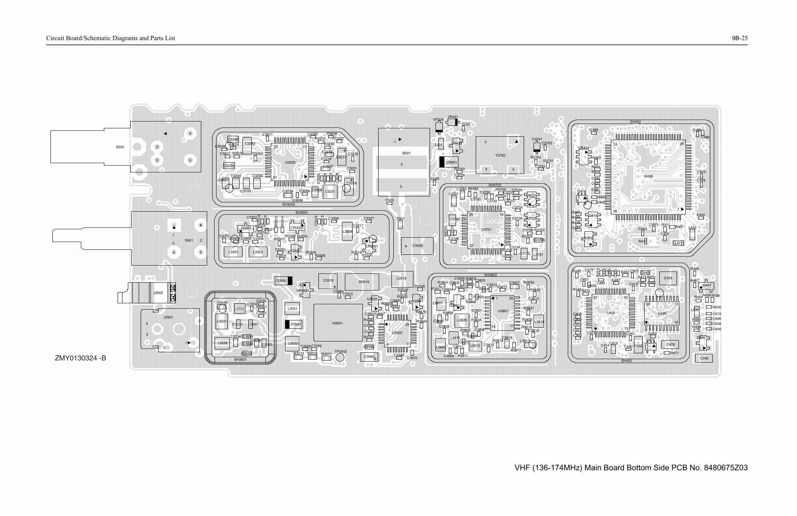
9B
-25
C3815
C3818
C3827
C3816
L3816
L3813
R3817
R3818
R3829
R3830R3812
R3831
R3816
R3832
SH3802
U3801
10
201
11
C3813C3823
3803
3808R3825
3803
R3826
C3812
C3821
C3806
0L3812
05
R3806
R3824
2
43
2
Y3762
C3751
C3763D3761
R3761R3760
1325
37 1
U3701
C3701C3702
C3703
C3704
C3731
C3732
C3734
C3708
C3709
C3725
C3705
C3761 C3707
C3733
D3701
D3702
L3731R3726
R3702
R3703
R3704
R3762
R3705
SH3702 C433
C435
C431
C494
C489
CR414
Q418
34
R414R415
R460
R463
SH402
C434
Q419R461R462
R419
76
U410
U409
2651
1
C449
C463
E400
C486
C488
C453C456
C493L410
L411
R411R457
R432
C407
C479
C481
R41
3
R475R425
R445
R449
C42
0 C422
C416
C42
1
C447C487
C442
C41
9
R400
R423
R472R473
13
2537
1
U404 U420
10
20
1
11
C475
C409
C411
C414
C410
C412
C443
C408
C415
C450
C476C430 C452
C451
Q410
34
R471
SH403
C458
C459
C466
C440
C473L400
Q420
Q421
R436R438
R439
R495
R496
R467
R434
R435
VHF (136-174MHz) Main Board Bottom Side PCB No. 8480675Z03
Circuit Board/Schematic Diagrams and Parts List
2S502
3 5
4
C3221
C3227
C32
28
C3236
C3244
C3219
C3222
C3223
C3224
C3226
C3229
C3237C3211
C3218C32
20
C3230
C3231C3232
C3233
C3234
C3235
C3240
C3238C3239
C3243
C3241
C3242
L3221
R3222
R32
20
R3224
R3223
R3219
R32
21
SH3202
1325
37 1
U3220
1
2
S501 C
8
C
4C3326
C3322
C33
23
C3325
C3305C3321
C33
24
C3301C3302 C3304C3303
CR3302D3301
L3301 L3303 Q3301
R3303
R3304
R33
14
R3306 R3324R3307
R33
15
SH3301
C3337
C33
15 C3339
C33
16
C3317
CR3301
L3308
R3305R3319
R3320
J3501
4
3
2
J3502
1
C3552
C3532
C3524
C3525C3528
C3531
C3533
C3534 C3535
C3536
C3550
C3551L3552
L3531
L3532
R3551
SH3501
C3526C3569
D3521
L3523
L3551
R3571R3572R3573
C3515
C3516
C3564
D3551 R3519
VR3501
H3501
TP3502
C3566
C3508
C3561
C3560
C3565
C3509
C3567
C3570
C3562
C3563
C3568
L3519
Q3561
R3570
R3569
R3562
R3561R3563
R3564
R3565
25
9 17
U3502
1
U3503
C
C3801
C3805C3802
L3801Q3801
R3804
R
R3807
R3801R
C3811
C3804
C381
C3808
C3809
L3826
L3811
L3809
R38
R3802
R3811
B501
3
2
1
C503
C52
C3735C500
CR501
L505
R3763
VR441VR506
VR439
C37
27
C3762
C3755
C3726
L3701
R37
27
F501
C3336
ZMY0130324 -B

Circuit Board/Schematic Diagrams and Parts List
6.8VVR431
INT_MIC
0.1uFC515 C524
1000pFC523100pF
R51010K
1000pFC520 C455
470pF100pFC454
1000pF.022uFC529
C5301000pF C446
100pFC499 C498
100pF1000pFC518
1000pFC519
1000pFC531
VR43210V 10V
VR43323
1
23
1
MIC
1M1
2M2
3M3
S1 7
S3 6
5S4
S24
C509 C504C508100pF 100pF100pF 1000pF
C501C4771000pF 1000pF
C478
VR45010.0V
VR45110.0V
C5161000pF 1000pF
C517
INT_SPN
SPN
SPP
SCI
ZMY0130312-D
9B-26
0.47uFC502
MECH_SWB+
TAB1
TAB2
5
3
HIG
H
2
SWITCH
4
1
LOW
S502
Vdda
VOL
0R507
6.8VVR501
C505100pF
UNSWB+
6
7 CR501
3AF501
21
10VVR439
100pFC503
1000pFC500
BATT_CODE
6.8VVR506
L505390nH
SWB+Vdda
B501
RSSI_FIL2
NEG1
POS3
SB1
PTT
SB2
RED_LED
Q502
CR503
180R502
2 4
1 3
R501680
51
6
24
3
IMX1
R50510K
Q505 47KR506
GREEN_LED
C5071000pF
C506100pF
RTA3
RTA2
RTA0RTA1
C514100pF100pF
C513100pF
C512100pFC511 7
GND GND19
1PC02PC14 PC2 PC3
8
S501SWITCH
C0 C0C1C1
C5281000pF
C527100pF
C5261000pF100pF
C525
5V
ANT_BIAS
Q506
4.7K
47K
47K
10K
.01uFC521
2
6.8VVR440
1SWITCHPB501
6.8VVR444
2 1
SWITCHPB504
.01uFC522
VR4416.8V
PB502
12SWITCH
J407
VHF Controls And Switches Schematic Diagram

9B
-27
NU
NUStripline
NU
NU
6.8pFC3314
C331510pF
C331620pF
C331739pF
10nHL3308
10pFC3339
.022uFC3318
C33192.7pF
3
1
2
T3301
XFMR
4
6
mgc_comps
R33201K
1KR3319
2
34
1
CR3301
IFifIF_1_FE
L3309 150nH
150R3321 R3322
220
18R3323
C332091pF
C3334
XFMR
T3302
4
6
3
1
2
mgc_comps
C333522pF
33nHL3312
20pF
TP3301
1
11
SH3303SHIELD
1
SH3302SHIELD
SH3301SHIELD
R3318470
ZMY0130321-B
VHF Receiver Front End Schematic Diagram
Circuit Board/Schematic Diagrams and Parts List
NU
NU
NU
Stripline
NUStripline
UNSWB+
C333610uF
UNSWB_PLUS_1_RX
if
ifUNSWB_PLUS_2_RX
.022uFC3337 R3316
4700.1uFC3309
ifR5_2_FE
ifR5_3_FE
R5
470nHL3304
330pFC3308
0.1uFC3306
330R3315
Q3302
10KR3310
3.3KR3308
100pFC3307
22R3313
R331233R3311
10
5.6KR3309
C3304150pF
CR3303
C3305
470pFC3338
R330733K
1pFC3310
150pFC3311
10R3314
L330512nH
CR3302SMBV1032
16pFC3312
D3302
L330612nH
150pFC3313
C3331C3330100pF100pF330pF
C3329
100KR3317
C333239pF
2.2KR3306
1000pFC3325 C3327
330pFQ3301
0.1uFC3326
100KR3304
R33242201K68K
R3305
ifRSSI_1_FE
RSSI
D3301
150pFC3302
L330312nH
ifRX_IN_1_FE
L330112nH
15pFC3303
RX_IN
C33015.6pF
330pFC3321
33pFC3324
100pFC3322
100KR3303
C3323100pF
RX_INJ
ifDACRx
DACRx_1_FE
if
RX_INJ_1_FE
DUMMY

Circuit Board/Schematic Diagrams and Parts List
NU
275.9K
C32780.1uF
0pF
R32741K
C32791uF
CLK
LVZ
IF_S
EL
16.8
MH
z
DA
TA
2
F44
Vdd_FILTEREDd_FILTERED
C322010pF
R32204.7K
1uHL3221
C3228.01uF C3229
100pF .022uFC3239
C32260.1uF
C32250.1uF
0.15uFC3238
1uFC3232
1uFC3233C3234
1uFC32311uF
C32350.22uF
0.1uFC3224
100pFC3237
.01uFC32360.22uF
C3240R3224
10
R32231K
SQ_OUT_1_ZIFif
DEMOD_1_ZIFif
SQ_OUT
DEMOD
Vdd_FILTERED
Vdd_FILTERED
SHIELDSH3202
1
LVZIF_SEL_1_ZIFif
CLK_3_ZIF
DATA_3_ZIF
if
if
if16_8MHz_3_ZIF
0.1uFC3223.01uF
C3227
1200pFC3241
0.1uFC3242
SH3203SHIELD
1 2 3
NU
RSSI_FLT5 RSSI_OUT4
TE
ST
A16
TESTD8
VAG32
VAG_REF25
VPP9
PHASE_LOCK26
PR
EA
MP
_OU
T47
PR
E_A
GC
48
PRE_IN3
RED_VCC1
RED_VSS2
ROSE_VCC30
ROSE_VSS29
GO
LD_V
SS
14
GR
EE
N_V
CC
41
GR
EE
N_V
SS
43
15IO
UT
31LIM
42M
IX_B
YP
46M
IX_I
N
MLP
D_C
R2417
DA
TA
DEMOD_HF28
DEMOD_OUT27
EMIT11
EXTBS6
21F
RE
FG
ND
20
GOLD_VCC10
C2P
39
C3M35
C3P
38
C4M36C
4P37
19C
EX
18C
LK
CO
L13
BASE12
BLU
E_V
CC
45
BLU
E_V
SS
44
BR
OW
N_V
CC
22 23B
RP
_OF
F
C1M33
C1P
40
C2M34
mgc_compsU3220
AFC7
32D83
ZMY0130407-A
9B-28
(SOURCE)
NUNU
RSSI
R3206100K
R3208100
R320739K
0.1uFC3208
Q3201
XTALY3200
1KR3209
16pFC3200
IF_1_ZIF
C32011.5pF
L32001uH
IF OUT 3IN6G
ND
1
GN
D1
2
GN
D2
4
GN
D3
5 1uHL3201
12pFC3202
RSSI
R32112.2K
RSSI2.2K
R3213
if
RSSI_2_ZIFRSSI_1_ZIF
if
C32091uF
R5
R32012.2K
R3200150
C3204.01uF
C32050.1uF
if R5_3_ZIF
1000pFC3210
1uHL3202
C3203100pF
R32024.7K R3210
2.2K
R32124.7K
MMBR941Q3200
22R3204
10KR3203
.01uFC3206
1KR3205 C3207
2.2pF
.01uF
C3221C32184.7uF
C3230100pF
5V
VSFif
VSF_3_ZIF
C32140.1uF
1K
R3225
Q3202
5V_3_ZIF
if5V
R3217
104.7uFC3211
R3214100
SWB_PLUS_3_ZIF
ifR3215
100
10pFC3215
SWB+
1uF C3212
Vdd_FILTERED
R3218
GN
D
2
4NCON_OFF*3
VIN1
VOUT5
LP2980U3201
C32134.7uF
if
Vdda_3_ZIF
Vdda
Vdd_FILTERED
C3271330pF
.022uFC3270
10R3226
R327147
10pFC3273
C32724.7pF
Q3270BFQ67W
1
3
2
33pFC3274
100nHL3270R3273
47K
1KR3270 C3275
56pF
R327247K C3276
47pF 82pFC3277
2.2uHL3271 R3
3
C3288200R3276
200KD3270
SH3201
1
SHIELD
C32190.1uF
100R3219
Vdd_FILTERED
0.1uFC322
100KR3222
.022uFC3243
.01uC32
5V
Vd
R3221100
5V
VHF Receiver Back End Schematic Diagram

9B
-29
WARP
XTAL1XTAL2
TEST1TEST2
VMULT1VMULT2VMULT3VMULT4
SFOUT
MODOUTFREFOUT
IADAPT
INDMULT
IOUT
LOCK
AUX3AUX4
ADAPTSW
AUX1AUX2
VR
OV
CP
PR
E_V
DD
PD
_VD
D
DV
DD
AV
DD
VBPASSPVREF
REFSEL
SFBASESFCAP
SFIN
MODIN
NC1NC2NC3
PREIN
DATA
BIAS1BIAS2
CCOMP
CEXCLK
PR
E_G
ND
PD
_GN
D
DG
ND
AG
ND
3344 622
1347 34 536 20
2135
18
2726
30
10
172931
32
7
4039
42
98
U370163A27
uF711
2NR
4OUT
3SD
6ERR
1
GN
D
5IN
ADP3300U3711
SWB_PLUS_1_FN
2.2uFC3713
C37120.1uF
SWB+
C3735NU
R3763NU
GN
D3
IN1
OUT2
16.8MHz 45J49Y3761
D3761
R376147K
NUR3760
.01uFC3731C3763
2F
AD
J
4GND
3O
UT
1VDD
1.6pF
NU
OSC_16.8MHZ16.8MHz
Y3762
C3751NU
5V
C37332.2uF
2.2uHL3731
C3734.01uF.01uF
C3732
VddaVdda_1_FN
220pF220pFC3745C3742
220pFC3744 C3743
220pF
CSX_1_FN
DATA_1_FN
MODIN_1_FN
CLK_1_FN
CLK
MODIN
DATA
CSX
C3753C3752
4.7uF1000pF 0.1uF
C3754
VSF_1_FN
VSF
PRESC_1_FN
8.2pFC3726
PRESC
2.2uFC3755
200KR3751
R3752330K
R3727100K
100pFC3727
TP37021
7.5V
2.5V - 3.5V
RMS
4.55V
3.3V
ZMY0130322-D
VHF Synthesizer Schematic Diagram
Circuit Board/Schematic Diagrams and Parts List
25
2324
3738
15141211
28
4119
45
16
43
4
23
46
481
TRB_1_FN
LOCK
TRB
LOCK_1_FN
220pFC3746
BIAS_ADJ_1_FN
BIAS_ADJ
NUNU
C3725R3726
100R3701
2.2uFC3710
390nHL3701
0.1uFC3709R3703
150
C370722pF
NUR3702
C37080.1uF
33K
K11
K22
K33
R3705D3702
A16
A25
A34
R3704150
A2 5A3
4
1 K1
2 K2
3 K3
D3701
A16
C3703.01uF
C3704.01uF
.01uFC3701
.01uFC3702
0.1uFC3705
C37064.7uF
470R3721
100pFC3716
100pFC3715
4.7uFC3714
1uFC3724
R3723100
TP3701 1
0.1uFC3722
1KR3722
0.1uFC3721
4
1
3
Q3721
2
UMC5N
R5
5V
T5_1_FN
R5_2_FN
VCTRL_1_FN
R5_1_FN
T5
VCTRL
4.7K47K
47K
10K
5V_1_FN5V (SOURCE)
10C3
VCO_MOD_1_FN
VCO_MOD
11
SH3702SHIELD
SH3701SHIELD
16_8MHz_1_FN16.8MHz
100R3741
NUC3741
330pFC3762R3762
NU
56pFC3761
13.2V
R: 5VT: 0V
R: 0VT: 5V
3.5 - 9.5V@135-174MHz
RF mV RMS measured with high impedance probe.
5V
120mV RMS
400mV
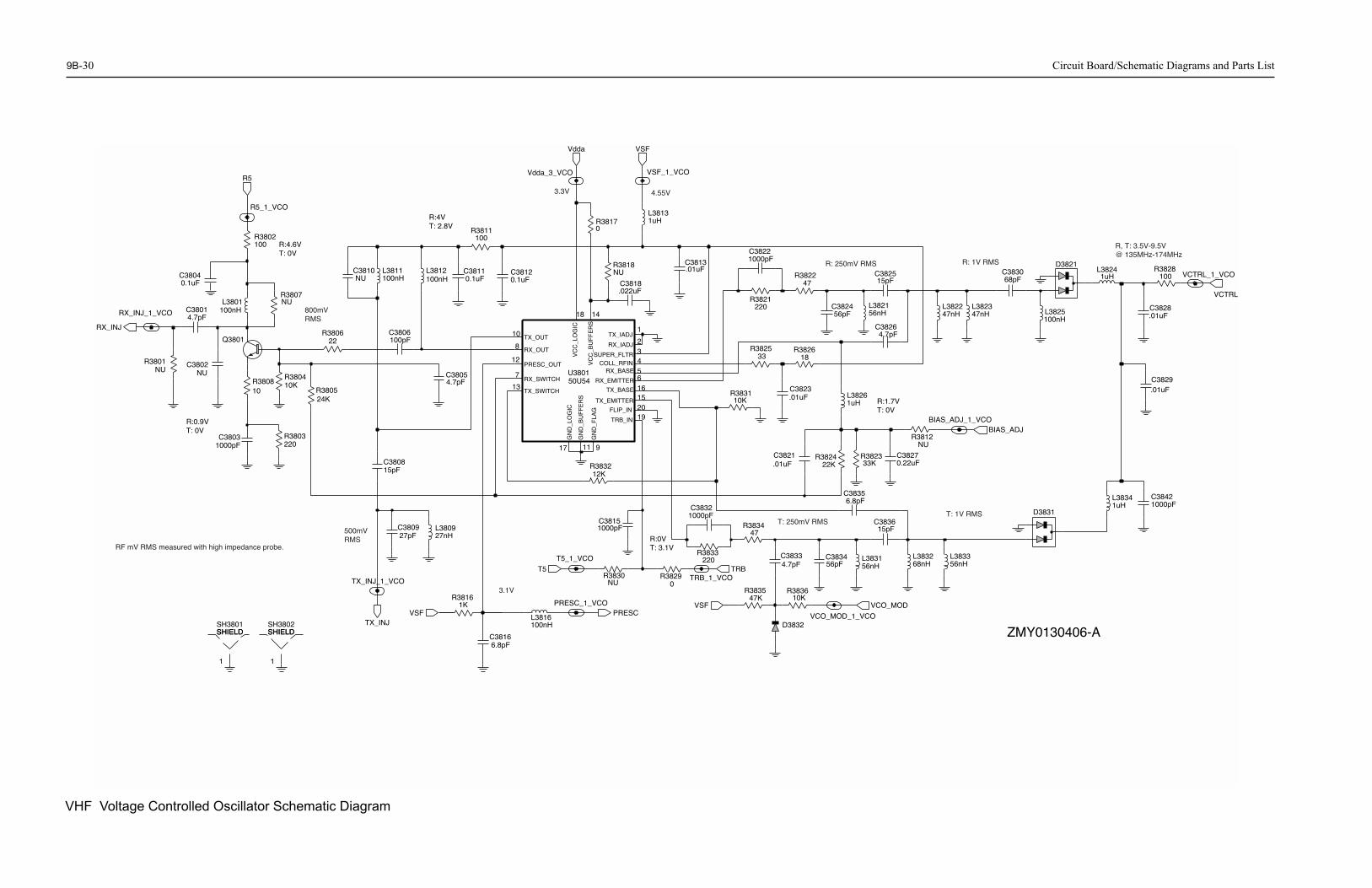
Circuit Board/Schematic Diagrams and Parts List
47822
15pFC3836
6.8pF
VCO_MOD_1_VCO
6
L383156nH 56nH
L383356pFC3834
VCO_MOD
L383268nH
C3835
C38264.7pF
826
C382456pF
L382156nH
L382247nH
C382515pF
C383068pF
L382347nH
NUR3812
L38261uH
BIAS_ADJBIAS_ADJ_1_VCO
0.22uFC3827
23F
33KR3823R3824
22K
L38241uH
L3825100nH
VCTRL_1_VCO
VCTRL
C3828.01uF
100R3828
.01uFC3829
D3821
L38341uH
C38421000pF
D3831
R: 250mV RMS R: 1V RMS
R, T: 3.5V-9.5V@ 135MHz-174MHz
R:1.7VT: 0V
T: 1V RMSV RMS
ZMY0130406-A
9B-30
R380524K
10R3808 10K
R3804
0.1uF
RX_INJ_1_VCO
C3804
Q3801
C38014.7pF
R3801 C3802NU
100nH
RX_INJ
L3801
NU
100R3802
R3807NU
R5_1_VCO
R5
C3806100pF
R380622
L3811100nH
C3810NU
L3812100nH 0.1uF
C3812
R3811100
C38110.1uF
VSF_1_VCO
Vdda
R38170
L38131uH
Vdda_3_VCO
VSF
C3813.01uF
R3818NU
C3818.022uF
C38221000pF
220R3821
R3
C38054.7pF
C38031000pF
R3803220
27nHL3809C3809
27pF
C380815pF
1
SHIELDSH3802SHIELD
1
SHIELDSH3801SHIELD
TX_INJ_1_VCO
1KR3816
T5
VSFPRESC_1_VCO
T5_1_VCO
L3816100nH
6.8pFC3816
TX_INJ
NUR3830
PRESC
1000pFC3832
12KR3832
1000pFC3815
VSF
220R3833
TRB_1_VCOR38290
R383547K
TRB
47R3834
4.7pFC3833
10KR383
D3832
1R38R3825
33
10KR3831
C38.01u
C3821.01uF
VC
C_L
OG
IC
SUPER_FLTR
TRB_IN
TX_BASE
TX_EMITTER
TX_IADJTX_OUT
TX_SWITCH
VC
C_B
UF
FE
RS
GN
D_F
LAG
GN
D_L
OG
IC
PRESC_OUTRX_BASE
RX_EMITTER
RX_IADJRX_OUT
RX_SWITCH
COLL_RFIN
FLIP_IN
GN
D_B
UF
FE
RS
U380150U54
18
3
19
1615
110
13
14
917
12
56
28
7
4
20
11
R:4.6VT: 0V
R:4VT: 2.8V
3.3V 4.55V
T: 250m
R:0VT: 3.1V
3.1V
500mVRMS
R:0.9VT: 0V
800mVRMS
RF mV RMS measured with high impedance probe.
VHF Voltage Controlled Oscillator Schematic Diagram

9B
-31
L352223.75nH
C352810pF
C352522pF
NUC3527
130pFC3523
20pFC3524
.022uFC3526
1uHL3523
120R3573
D3521
R3572120
R3571NU
C3569.022uF
ANT_BIAS
NUR3569
R3570NU
NUQ3561
UNSWB+
SH3502SHIELD
12pFC3531
L353134.14nH
9.1pFC3533
C353230pF
34.14nHL3532
C353524pF
10pFC3534
C353615pF
18pFC3537
GND 4
1
2
3
RF_JACKJ3501
ANTENNA_CONTACTJ3502
30.54nHL3538
18pFC3539
RX_INRX_IN_1_PA
C355256pF
91pFC3551
39R3551
7.66nHL3552
D355120pF
C3550
43.67nHL3551
0985613Z01
21
501
K1K2K3
CR3501
A1A2A3
ZMY0130323-D
VHF Transmitter Schematic Diagram
Circuit Board/Schematic Diagrams and Parts List
VG
6V
L19
VLI
M
2T
1
30TEMP
14V10
16V45V
5EX
T17
VA
R1
20
VA
R2
18
VA
R3
24
15
INT
NA
22
11Q
QX10
RF
IN1
21R
S
RSET31
23R
X
7C
L
26CLK
12CQ
CQX1328
DATA
9F168
GN
D1
8
GND225
4
32 ANO
BPOS27
29CEX
CI
3 5C
J
H99S-4U3502
C35601uF
3300pFC3562
330KR3564
R3565NU
C3565.022uF
C35633300pF
220pFC3564
1uFC3516
330pFC3567
C3519
C3518R3513
L3518
L351513.85nH
R35190.1
3300pFC3515
Microstrip
D
G
S
Q3501
7.66nHL3521
220pFC3521
UNSWB+UNSWB+
330pFC3570
5V_2_PARESET_1_PA
5VRESET
BIAS_TUNING
CLKUNSWB+ DATACSX
DATA_2_PA
CLK_2_PA
UNSWB_LPLUS_2_PA
CSX_2_PA
UNSW_LPLUS_3_PA
33KR3562
12KR3561
C3561.022uF
POS
VO
UT
2
U3503
GND3
100pFC3566 LM50C
5185963A15
L350468nH
270KR3563
C3508.022uF 330pF
C3509.022uF 68nH
L3503C3504
5.6nHL3501
C350333pF
C350233pF
18nHL3511
NUC3507C3506
NUNU
L3502
47pFC3512
R3541NU330pF
C3542
L351211.03nH
C351330pF
C3541.022uF BIAS_TUNING
TP3502
1
12KR3547
.022uFC3547
100R3544
100R3545
R354633K
C3546330pF
R35487.5K
H3501
1
HEATSINK
SHIELDSH3501
C3544330pF
100R3543
.022uFC3543
5.6KR3542
C3505330pF
6
7RFOUT21 VCNTRL14 VD1 2VG1
3VG2
GN
D3
12
GN
D4
13
8 NC19 NC2
10 NC315 NC4
16 RFIN RFOUT1
U3501
11 G2
GN
D1
4
GN
D2
5
C65
R3505470
R3503300
330pFC3501
300R3501
TX_INJ_1_PATX_INJ
18R3502
BEADL3519 C3568
3300pF
1
17E
P
R3512NU
R35063.9
R35073.9
L35137.66nH
C351468pF
68pFC3517
NU
NU
NU
NU
VR310V

Circuit Board/Schematic Diagrams and Parts List
330pF47pF30pF68pF3300pF1uF
220pF130pF20pF22pF22000pF, +80%/-20%GCAM Dummy Part Number10pF12pF30pF9.1pF10pF24pF15pF20pF18pF22000pF, +80%/-20%330pF22000pF, +80%/-20%330pF330pF22000pF, +80%/-20%20pF91pF56pF1uF22000pF, +80%/-20%3300pF3300pF220pF0.022uF100pF330pF3300pF22000pF, +80%/-20%330pF10000pF, 10%10000pF, 10%10000pF, 10%10000pF, 10%0.1uF4.7uF22pF100000pF, +80%/-20%
Description
C3709 2113743M24 100000pF, +80%/-20%C3710 2104993J02 2.2uFC3711 2311049A69 10uF, 20%C3712 2113743M24 100000pF, +80%/-20%C3713 2311049A09 2.2uFC3714 2311049J11 4.7uFC3715 2113743N50 100pFC3716 2113743N50 100pFC3721 2113743E20 0.1uFC3722 2113743E20 0.1uFC3724 2311049A08 1uFC3725 Not PlacedC3726 2113743N24 8.2pFC3727 2113743N50 100pFC3731 2113743L41 10000pF, 10%C3732 2113743L41 10000pF, 10%C3733 2104993J02 2.2uFC3734 2113743L41 10000pF, 10%C3735 Not PlacedC3741 Not PlacedC3742 2113743L01 220pFC3743 2113743L01 220pFC3744 2113743L01 220pFC3745 2113743L01 220pFC3746 2113743L01 220pFC3751 Not PlacedC3752 2113743L17 1000pFC3753 2311049A56 4.7uFC3754 2113743M24 100000pF, +80%/-20%C3755 2104993J02 2.2uFC3761 2113743N44 56pFC3762 2113740F63 330pFC3763 2113743N08 1.6pFC3801 2113743N18 4.7pFC3802 Not PlacedC3803 2113743L17 1000pFC3804 2113743E20 0.1uFC3805 2113743N18 4.7pFC3806 2113743N50 100pFC3808 2113743N30 15pFC3809 2113743N36 27pFC3810 Not PlacedC3811 2113743M24 100000pF, +80%/-20%C3812 2113743M24 100000pF, +80%/-20%C3813 2113743L41 10000pF, 10%C3815 2113743L17 1000pFC3816 2113743N22 6.8pFC3818 2113743E07 0.022uFC3821 2113743L41 10000pF, 10%C3822 2113743L17 1000pFC3823 2113743L41 10000pF, 10%
Circuit Ref
Motorola Part No.
Description
9B-32
VHF Radio Parts List
Circuit Ref
Motorola Part No.
Description
B501 0986237A02 Battery ContactC3200 2113743N31 16pFC3201 Not PlacedC3202 Not PlacedC3203 2113743N50 100pFC3204 2113743L41 10000pF, 10%C3205 2113928N01 0.1uFC3206 2113743L41 10000pF, 10%C3207 2113743N10 2.2pFC3208 Not PlacedC3209 2311049A07 1uFC3210 2113743L17 1000pFC3211 2311049A56 4.7uFC3212 2311049A07 1uFC3213 2311049A56 4.7uFC3214 2113928N01 0.1uFC3215 2113743N26 10pFC3218 2311049A56 4.7uFC3219 2113928N01 0.1uFC3220 2113743N26 10pFC3221 2113743L41 10000pF, 10%C3222 2113928N01 0.1uFC3223 2113928N01 0.1uFC3224 2113928N01 0.1uFC3225 2113928N01 0.1uFC3226 2113928N01 0.1uFC3227 2113743L41 10000pF, 10%C3228 2113743L41 10000pF, 10%C3229 2113743N50 100pFC3230 2113740F51 100pFC3231 2180478Z20 1uFC3232 2180478Z20 1uFC3233 2180478Z20 1uFC3234 2180478Z20 1uFC3235 2113743A23 0.22uFC3236 Not PlacedC3237 Not PlacedC3238 2113743A24 0.33uFC3239 2113743E07 0.022uFC3240 2113743A23 0.22uFC3241 2113743L19 1200pFC3242 2109720D14 0.1uF, 1206C3243 2113743E07 0.022uFC3244 2113743L41 10000pF, 10%C3270 2113743E07 0.022uFC3271 2113743L05 330pFC3272 2113743N18 4.7pFC3273 2113743N26 10pFC3274 2113743N38 33pF
C3275 2113743N44 56pFC3276 2113743N42 47pFC3277 2113743N48 82pFC3278 2113743E20 0.1uFC3279 2311049A07 1uFC3280 2113743L39 8200pFC3301 2113743N29 13pFC3302 2113743N54 150pFC3303 2113743N33 20pFC3304 2113743N54 150pFC3305 Not PlacedC3306 2113928N01 0.1uFC3307 2113743N50 100pFC3308 2113743L05 330pFC3309 2113928N01 0.1uFC3310 Not PlacedC3311 2113743N54 150pFC3312 2113743N31 16pFC3313 2113743N54 150pFC3314 Not PlacedC3315 2113743N26 10pFC3316 2113743N33 20pFC3317 2113743N40 39pFC3318 2113743M08 22000pF, +80%/-20%C3319 Not PlacedC3320 2113743N49 91pFC3321 2113743L05 330pFC3322 2113743N50 100pFC3323 2113743N50 100pFC3324 2113743N38 33pFC3325 2113743L17 1000pFC3326 Not PlacedC3327 2113743L05 330pFC3329 2113743L05 330pFC3330 2113743N50 100pFC3331 2113743N50 100pFC3332 2113743N40 39pFC3334 2113743N33 20pFC3335 2113743N34 22pFC3336 2311049A18 10uFC3337 2113743M08 22000pF, +80%/-20%C3338 2113743L09 470pFC3339 2113743N26 10pFC3501 2113743L05 330pFC3502 2113743N38 33pFC3503 2113743N38 33pFC3504 2113743M08 22000pF, +80%/-20%C3505 2113743N38 33pFC3506 Not PlacedC3507 Not PlacedC3508 2113743M08 22000pF, +80%/-20%
Circuit Ref
Motorola Part No.
Description
C3509 2113743L05C3512 2113740F43C3513 2113740F38C3514 2113740F47C3515 2113743L29C3516 2311049A08C3518 Not PlacedC3519 Not PlacedC3521 2111078B51C3523 2111078B45C3524 2113740F34C3525 2113740F35C3526 2113743M08C3527 Not PlacedC3528 2113740F27C3531 2113740F29C3532 2113740F38C3533 2113740F26C3534 2113740F27C3535 2113740F36C3536 2113740F31C3537 2113740F34C3539 2113740F33C3541 2113743M08C3542 2113743L05C3543 2113743M08C3544 2113743L05C3546 2113743L05C3547 2113743M08C3550 2113743N33C3551 2113743N49C3552 2113743N44C3560 2311049A07C3561 2113743M08C3562 2113743L29C3563 2113743L29C3564 2113743L01C3565 2113743E07C3566 2113743N50C3567 2113743L05C3568 2113743L29C3569 2113743M08C3570 2113743L05C3701 2113743L41C3702 2113743L41C3703 2113743L41C3704 2113743L41C3705 2113743E20C3706 2311049J11C3707 2113743N34C3708 2113743M24
Circuit Ref
Motorola Part No.

9B
-33
1000pF10000pF, 10%10000pF, 10%
0 100pF1000pF
0 100pF1000pF
0 100pF1000pF1000pF1000pF1000pFRing Quad Diode
6 Dual Bonds Pin Diode, RH Reeled
3 Dual Common Anode-Cath-ode
Schottky DiodeSchottky DiodeSchottky Diode
2 Dual Common Cathode Diode1 Rectifier9 LED Red/Yel1 Varactor8 Dual Diode8 Dual Diode2 Pin Diode2 Pin Diode
Triple DiodeTriple Diode
3 Varactor 3 Dual Varactor3 Dual Varactor1 Varactor1 Ferrite Bead1 3A Fuse1 Heat Spreader1 RF Jack1 Antenna Contact4 40-pin Connector2 4 pin Connector1 4 pin connector (Stereo Jack
2.5mm)1 3 pin connector (Mono Jack
3.5mm)8 1uH
8 1uH8 1uH5 100nH
.
Description
L3271 2462587Q20 2.2uHL3301 2462587T35 12nHL3303 2462587T35 12nHL3304 2462587T23 470nHL3305 2462587T35 12nHL3306 2462587T35 12nHL3308 2462587T34 10nHL3309 2462587N55 150nHL3312 2462587V28 33nHL3501 2413926H09 5.6nHL3502 Not PlacedL3503 2462587V32 68nHL3504 2462587N51 68nHL3511 2462587N44 18nHL3512 2479990B01 11.03nHL3513 2479990A02 7.66nHL3515 2479990C03 13.85nHL3518 Not PlacedL3519 2484657R01 BeadL3521 2479990A02 7.66nHL3522 2479990E01 23.75nHL3523 2462587N68 1uHL3531 2460591N28 34.14nHL3532 2460591N28 34.14nHL3538 2479990M01 30.54nHL3551 2479990N01 43.67nHL3552 2479990A02 7.66nHL3701 2462587Q42 390nHL3731 2462587Q20 2.2uHL3801 2462587V34 100nHL3809 2462587V27 27nHL3811 2462587V34 100nHL3812 2462587V34 100nHL3813 2462587Q47 1uHL3816 2462587V34 100nHL3821 2462587N50 56nHL3822 2462587N49 47nHL3823 2462587N49 47nHL3824 2462587N68 1uHL3825 2462587V34 100nHL3826 2462587N68 1uHL3831 2462587N50 56nHL3832 2462587N51 68nHL3833 2462587N50 56nHL3834 2462587N68 1uHL400 2462587Q42 390nHL410 2462587Q42 390nHL411 2462587Q42 390nHL505 2462587Q42 390nHPB501 4080523Z01 Tactile Push ButtonPB502 4080523Z01 Tactile Push Button
Circuit Ref
Motorola Part No.
Description
Circuit Board/Schematic Diagrams and Parts List
C3824 2113743N44 56pFC3825 2113743N30 15pFC3826 2113743N18 4.7pFC3827 2113743E07 0.022uFC3828 2185895Z01 0.01uFC3829 2185895Z01 0.01uFC3830 2113743N46 68pFC3832 2113743L17 1000pFC3833 2113743N18 4.7pFC3834 2113743N44 56pFC3835 2113743N22 6.8pFC3836 2113743N30 15pFC3842 2113743L17 1000pFC400 2113743L41 10000pF, 10%C401 2113743M24 100000pF, +80%/-20%C402 2113743M24 100000pF, +80%/-20%C403 2113928D08 10uF, +80%/-20%C407 2113928N01 0.1uFC408 2113743N50 100pFC409 2113743M24 100000pF, +80%/-20%C410 2113928N01 0.1uFC411 2113743M24 100000pF, +80%/-20%C412 2113928N01 0.1uFC414 2113743M24 100000pF, +80%/-20%C415 2185895Z01 0.01uFC416 2113928N01 0.1uFC419 2113743L41 10000pF, 10%C420 2113743L41 10000pF, 10%C421 2113928N01 0.1uFC422 2113743M24 100000pF, +80%/-20%C423 2113743N50 100pFC424 2311049A59 10uF, 10%C425 2113743M24 100000pF, +80%/-20%C426 2113743N50 100pFC427 2113743N50 100pFC428 2113743M24 100000pF, +80%/-20%C429 2113743M24 100000pF, +80%/-20%C430 2113928N01 0.1uFC431 2113743N50 100pFC432 Not PlacedC433 2113743L41 10000pF, 10%C434 2113743M24 100000pF, +80%/-20%C435 2113743M24 100000pF, +80%/-20%C440 2113743G26 4.7uF, +80%/-20%C442 2113743E20 0.1uFC443 2113928N01 0.1uFC446 2113743M08 22000pF, +80%/-20%C447 2113928N01 0.1uFC449 2113743N50 100pFC450 Not PlacedC451 2113743M08 22000pF, +80%/-20%
Circuit Ref
Motorola Part No.
Description
C452 2113743G26 4.7uF, +80%/-20%C453 2113743N50 100pFC454 2113743N50 100pFC455 2113743L09 470pFC456 2113743N50 100pFC458 2113743N50 100pFC459 2113743N50 100pFC463 2113743N50 100pFC466 2113743N50 100pFC467 2113928N01 0.1uFC471 2113743N50 100pFC472 2113743N50 100pFC473 2113743L09 470pFC475 2113743H14 10uF, +80%/-20%C476 2113928D08 10uF, +80%/-20%C477 2113743N50 100pFC478 2113743N50 100pFC479 2113928N01 0.1uFC480 2113928D08 10uF, +80%/-20%C481 2113928N01 0.1uFC482 2113928N01 0.1uFC483 2113743L17 1000pFC484 2113743L17 1000pFC485 2113743L17 1000pFC486 Not PlacedC487 Not PlacedC488 Not PlacedC489 Not PlacedC493 Not PlacedC494 2113743N50 100pFC498 2113743N50 100pFC499 2113743N50 100pFC500 2113743L17 1000pFC501 2113743L17 1000pFC502 2311049A05 0.47uF, 10%, 25VC503 2113743N50 100pFC504 2113743L17 1000pFC505 2113743N50 100pFC506 2113743N50 100pFC507 2113743L17 1000pFC508 2113743N50 100pFC509 2113743L17 1000pFC511 2113743N50 100pFC512 2113743N50 100pFC513 2113743N50 100pFC514 2113743N50 100pFC515 2113743M24 100000pF, +80%/-20%C516 2113743L17 1000pFC517 2113743L17 1000pFC518 2113743L17 1000pFC519 2113743L17 1000pF
Circuit Ref
Motorola Part No.
Description
C520 2113743L17C521 2113743L41C522 2113743L41C523 2113743N5C524 2113743L17C525 2113743N5C526 2113743L17C527 2113743N5C528 2113743L17C529 2113743L17C530 2113743L17C531 2113743L17CR3301 4802245J42CR3302 4805129M9
CR3303 4880154K0
CR3501 Not PlacedCR412 4802245J62CR413 4802245J62CR414 4802245J62CR440 4813833C0CR501 4880107R0CR503 4805729G4D3270 4862824C0D3301 4802081B5D3302 4802081B5D3521 4880973Z0D3551 4880973Z0D3701 4802233J09D3702 4802233J09D3761 4862824C0D3821 4805649Q1D3831 4805649Q1D3832 4862824C0E400 2480640Z0F501 6580542Z0H3501 2680499Z0J3501 0985613Z0J3502 3980686Z0J400 0905505Y0J402 2809926G0J404 0980689Z0
J407 0980688Z0
L3200 2462587N6L3201 Not PlacedL3202 2462587N6L3221 2462587N6L3270 2462587T1
Circuit Ref
MotorolaPart No

Circuit Board/Schematic Diagrams and Parts List
120120100
15015033K4701000100
100K 100200K330K
47K
10022010K 24K 22
10100
10000
2204733K22K33181000
10K 12K2204747K 10K
Description
R400 0662057N15 47K R401 0662057M01 0R402 Not PlacedR403 Not PlacedR405 0662057M01 0R406 0662057N20 75KR408 Not PlacedR410 0662057N23 100K R411 0662057M98 10K R413 0662057M01 0R414 0662057V34 180KR415 0662057V26 91KR416 0662057M98 10K R418 0662057M01 0R419 0662057M90 4700R423 0662057N39 470KR425 0662057N10 30KR427 0662057M98 10K R428 0662057M10 2.2R429 0662057M98 10K R432 0662057N16 51KR434 Not PlacedR435 0662057M81 2000R436 0662057N15 47K R437 Not PlacedR438 0662057M01 0R439 0662057N23 100K R445 0662057N08 24K R446 Not PlacedR447 0662057N23 100K R448 0662057M98 10K R449 0662057N08 24K R451 0662057N03 15KR452 0662057N23 100K R454 Not PlacedR455 Not PlacedR456 0662057M01 0R457 0662057M98 10K R460 0662057M90 4700R461 0662057N23 100K R462 0662057N23 100K R463 0662057M61 300R467 0662057M98 10K R471 0662057N06 20KR472 0662057N12 36K R473 0662057M26 10R475 0662057M01 0R476 0662057N08 24K R478 0662057M98 10K
5480678Z01 Barcode LabelR492 0662057M01 0
Circuit Ref
Motorola Part No.
Description
9B-34
PB504 4080523Z01 Tactile Push ButtonQ3200 4813827A07 NPN TransistorQ3201 4880214G02 NPN TransistorQ3202 4880214G02 NPN TransistorQ3270 4805218N63 RF TransistorQ3301 4880214G02 NPN TransistorQ3302 4813827A07 NPN TransistorQ3501 4813828A08 RF Power FETQ3561 Not PlacedQ3721 4802245J50 Dual NPN/PNP TransistorQ3801 4813827A07 NPN TransistorQ400 4809579E18 MOSFET P-ChannelQ403 4813824A17 PNP TransistorQ405 4802245J54 Dual NPN TransistorQ410 4802245J54 Dual NPN TransistorQ417 4802245J50 Dual NPN/PNP TransistorQ418 4802245J50 Dual NPN/PNP TransistorQ419 5180159R01 Dual NPN TransistorQ420 4805128M67 PNP TransistorQ421 4880214G02 NPN TransistorQ431 5180159R01 Dual NPN TransistorQ433 4880214G02 NPN TransistorQ502 5180159R01 Dual NPN TransistorQ505 4880214G02 NPN TransistorQ506 4802245J50 Dual NPN/PNP TransistorR3200 0662057M54 150R3201 0662057M82 2200R3202 0662057M90 4700R3203 0662057M98 10K R3204 0662057M34 22R3205 0662057M74 1000R3206 0662057N23 100K R3207 0662057N13 39K R3208 0662057M50 100R3209 0662057M74 1000R3210 0662057M82 2200R3211 0662057M82 2200R3212 0662057M90 4700R3213 0662057M82 2200R3214 0662057M50 100R3215 0662057M50 100R3217 Not PlacedR3218 Not PlacedR3219 0662057M50 100R3220 0662057M90 4700R3221 0662057M50 100R3222 Not PlacedR3223 Not PlacedR3224 0662057M26 10R3225 0662057M74 1000R3226 0662057M26 10
Circuit Ref
Motorola Part No.
Description
R3270 0662057M74 1000R3271 0662057M42 47R3272 0662057N15 47K R3273 0662057N15 47K R3274 0662057M74 1000R3275 0662057M88 3900R3276 0662057N30 200KR3303 0662057N23 100K R3304 0662057N23 100K R3305 0662057N19 68K R3306 0662057M82 2200R3307 0662057N11 33KR3308 0662057M86 3300R3309 0662057M92 5600R3310 0662057M98 10K R3311 0662057M26 10R3312 Not PlacedR3313 0662057M34 22R3314 0662057M26 10R3315 0662057M62 330R3316 0662057M61 300R3317 0662057N23 100K R3318 0662057M66 470R3319 Not PlacedR3320 Not PlacedR3321 0662057M54 150R3322 0662057M58 220R3323 0662057M32 18R3324 0662057M58 220R3501 0662057M61 300R3502 0662057M32 18R3503 0662057M61 300R3505 0662057M62 330R3506 0662057B62 3.9R3507 0662057B62 3.9R3512 Not PlacedR3513 Not PlacedR3519 0680539Z01 0.1R3541 0662057N13 39K R3542 0662057M92 5600R3543 0662057M50 100R3544 0662057A25 100R3545 0662057A25 100R3546 0662057N01 12KR3547 0662057N11 33KR3548 0662057N07 22KR3551 0662057M40 39R3561 0662057N01 12KR3562 0662057N11 33KR3563 0662057N33 270K R3564 0662057N35 330K
Circuit Ref
Motorola Part No.
Description
R3565 Not PlacedR3569 Not PlacedR3570 Not PlacedR3571 Not PlacedR3572 0662057A27R3573 0662057A27R3701 0662057M50R3702 Not PlacedR3703 0662057M54R3704 0662057M54R3705 0662057N11R3721 0662057M66R3722 0662057M74R3723 0662057M50R3726 Not PlacedR3727 0662057N23R3741 0662057M50R3751 0662057N30R3752 0662057N35R3760 Not PlacedR3761 0662057N15R3762 Not PlacedR3763 Not PlacedR3801 Not PlacedR3802 0662057M50R3803 0662057M58R3804 0662057M98R3805 0662057N08R3806 0662057M34R3807 Not PlacedR3808 0662057M26R3811 0662057M50R3812 Not PlacedR3816 0662057M74R3817 0662057M01R3818 Not PlacedR3821 0662057M58R3822 0662057M42R3823 0662057N11R3824 0662057N07R3825 0662057M38R3826 0662057M32R3828 0662057M50R3829 0662057M01R3830 Not PlacedR3831 0662057M98R3832 0662057N01R3833 0662057M58R3834 0662057M42R3835 0662057N15R3836 0662057M98
Circuit Ref
Motorola Part No.

9B
-35
Circuit Board/Schematic Diagrams and Parts List
* Motorola Depot Servicing only
R493 Not PlacedR494 0662057M01 0R495 0662057N23 100K R496 0662057N23 100K R498 0662057N23 100K R499 0662057M98 10K R501 0662057M70 680R502 0662057M56 180R505 0662057M98 10K R506 0662057N15 47K R507 0662057M01 0R510 0662057M98 10K RT400 0680590Z01 Thermistor 33KS501 4080710Z01 Channel SwitchS502 1880619Z02 Volume SwitchSH3201 2602023X08 Rx Back end top shieldSH3202 2686081B02 LVZIF ShieldSH3203 2686081B03 45.1MHz Xtal ShieldSH3301 2686081B01 Rx Back end bottom shieldSH3302 2686081B05 Mixer ShieldSH3303 2686081B06 Rx Front end top shieldSH3501 2680687Z01 Shield, Harmonic FilterSH3502 2686081B04 PA Driver ShieldSH3701 2680511Z01 Synthesizer Top ShieldSH3702 2680511Z01 Synthesizer Bottom ShieldSH3801 2680513Z01 Shield, VCO TopSH3802 2680514Z01 Shield, VCO BottomSH400 2680505Z01 Controller Memory ShieldSH401 2680506Z01 On/off Controller ShieldSH402 2680515Z01 Microprocessor ShieldSH403 2680516Z01 ASFIC CMP/Audio PA Con-
troller ShieldT3301 2580541Z01 XFMR CoilT3302 2580541Z01 XFMR CoilU3201 5102463J58 3.3V Voltage RegulatorU3220 5109632D83 LVZIF ICU3501 5185130C65 LDMOS Driver ICU3502 5185765B28 Power Control ICU3503 5185963A15 Temperature SenseU3701 5185963A27 LVFRACN Synthesizer ICU3711 5105739X05 5V RegulatorU3801 5105750U54 VCO Buffer ICU400 5102463J40 3.3V Voltage RegulatorU404 5185130C53 ASFIC_CMPU405 Not PlacedU406 *5102463J59 Flash ROM 128K X 8U407 *5102463J64 16K X 8 EEPROMU409 5102226J56 MicroprocessorU410 5102463J57 3.3V Voltage RegulatorU420 5102463J44 Audio PAVR3501 4880140L15 Zener diode, 10V
Circuit Ref
Motorola Part No.
Description
VR431 4802245J73 Zener Diode, 6.8VVR432 4880140L15 Zener Diode, 10VVR433 4880140L15 Zener Diode, 10VVR439 4880140L15 Zener Diode, 10VVR440 4802245J73 Zener Diode, 6.8VVR441 4802245J73 Zener Diode, 6.8VVR444 4802245J73 Zener Diode, 6.8VVR450 4802245J75 Zener Diode, 12.0VVR451 4802245J74 Zener Diode, 10.0VVR501 4813830A18 Zener Diode, 6.8VVR506 4802245J73 Zener Diode, 6.8VY3200 4802245J43 Xtal FilterY3761 4805875Z04 16.8MHz Crystal OscillatorY3762 Not Placed
5480678Z01 Barcode Label8480675Z03 VHF main PC board
Circuit Ref
Motorola Part No.
Description

Circuit Board/Schematic Diagrams and Parts List
2
3
4PB504
C32
04
C32
06
C32
07C
3208
C3210
L3202
Q32
00Q
3201
R3201
R3202
4
R32
06
R3209
R32
10
R3212 C32
09
C3214
C32
15
Q32
02
R3213
R32
14
R32
15
R3217
R32
18
R3225
U32
01
C32
25
C3270
C32
71
C32
72
C32
73
C32
74
C32
75
C32
76
C3277
C3278
C3279 C32
80
D32
70
L327
0
L327
1
Q3270
R3226
R32
70
R32
71
R32
72
R32
73
R3274
R3275
R32
76
SH3201
C3212 C3213
C50
2
C50
5C52
1
2
3
4PB501
2
3
4PB502
VR440
C50
6C
507
C512
C513
4 3
2CR503 Q502
Q505
R50
1R
502
R50
5
R50
6
R50
7
VR501
C477
C47
8 C50
1C
504
C50
8
C509
C51
1
C51
4
C3537
C35
39
CR
3501
L3538
45
2
3
6
7
J407
C454
C498
C49
9C
518
C519
C520
VR432
VR
433
C3318
C33
29
6
43
T3301 C33
06
C33
07
C33
10C3311
C3312
C3313C3314
C3327
C3330
C33
31
C33
32
C33
38
CR
3303
D3302
L3305L3306
Q3302
R33
08
R33
09R
3310
R3311
R3312
R3313SH3303
C33
08
C33
09
L3304
R3316
C33
19
R3317
C3521 C3523L3515
L3521
12 3
Q3501
C3518
C35
19
C35
27
C35
46
L3518
L352
2
R35
12
R35
13
R35
44R
3546
R35
47
3548H3502
9B-36
9.0 Circuit Board/Schematic Diagrams and Parts List
1
J400
40
TP401
C424
C425C426
C427 C428
C429
R408
R428
R42
9
R478
R49
2
SH400
1
1
45
8
U407
RT400
16
2271
R41
8
218
U405
17
U406
32
C42
3 R410
R437
C43
2
C529C531
TP3702
6 4
31
Y3761 C45
5C
515
C51
6
C517
C52
3
C52
4
C52
5
C52
6
4 3Q506
VR431VR450
VR451
C44
6
C527C528
TP3701
C53
0
C3205 R3200
VR444
C3200C3201
C32
02
C3203
L3200
L320
1
R32
03
R320
R32
05R
3207
R32
08
R32
11
SH3203
Y3200
C47
0
C471
C472
C483C484
C48
5
CR
413
2
1
3
4
6
5
J402
4 3
Q41
7
Q431
Q43
3
R49
3
R49
4
R49
8
R49
9
TP402
TP405 TP406
TP410
C40
0
C40
1
C402
C403
C467
C48
0
C48
2
CR412
CR
440
Q40
0
Q403
43
Q405
R401
R40
2
R40
3
R405
R40
6
R41
6
R427
R446
R44
7
R44
8R
451
R45
2 R454
R45
5
R45
6
R476
R481
SH401TP415
4
5 8
U400
C38
22
C3824
C3825
C38
26
C38
28
C38
29
C3830
C3832 C3833
C3834
C38
35
C3836
C38
42
D3821D3831
D38
32
L3821
L3822
L3823
L3824
L3825
L3831
L3832 L3833
L3834
R38
21
R3822
R38
23
R38
28
R3833 R3834R
3835
R38
36
SH3801
C3714
C3741
C3742
R3741
C3706
C37
52
C37
53
C37
54
R3721R37
51
R3752
SH3701
C3710
C37
11
C3713
C37
21
C3722
C37
24
C3743
C3744
C3745
C3746 43
Q3721
R3722
R3723
U3711C3716
R3701
C3712C3715
C33
20
C3334
C33
35
L3309
L3312
R3318
R3321
R3322
R3323
SH3302
6
4 3
T3302
TP3301
C3512
C3513
C3514
C3517
L3504
L3511 L3512
L3513
R3506
R3507
1
16
8
9
U3501
C3501
C3502
C3503
C3504
C3505
C35
41
C35
42
C35
43
C35
44
C35
47
L350
3
R3501
R3502 R3503
R35
05
R35
41
R35
42
R35
43
R35
45
RS
L3501
R51
0
VHF (136-174MHz) Main Board Top Side PCB No. 8480675Z04

9B
-37
C3803
C38
05
C38
06
C38
10
C38
11
C38
12C
3813
C3815
C38
16
C38
18
C38
21C
3823 C3827
1
L3812 L3813
L3816L3826
Q38
01
R3803
R3804
R3805
R38
06R
3808
R38
11
R3812
R38
16
R38
17
R38
18
R38
24R
3825
R38
26
R38
29R38
30R
3831
R3832
SH3802
11
1 20
10
U38
01
C40
7
C408
C409
C410
C41
1
C412
C41
4
C41
5
C41
6C
422
C430
C442
C443
C447
C450
C45
1
C45
2
C475
C476
C47
9
C481C487
43
Q410
R400
R423
R42
5
R44
5
R44
9
R471
R472R473
R475
SH403
1
37 25
13
U404
11
1
20
10
U420
C440
C458
C459
C466C473L4
00Q
420
Q421
R434
R435
R43
6
R43
8
R439
R46
7R
495
R496
C41
9
C42
0
C42
1
R41
3
C52
2
C3735
R3763
VR
439
1
2
3 4
Y3762
C3751
C37
63
D37
61R
3760
R37
61
C3701
C3702
C3703
C3704
C3705
C37
07
C3708
C37
09
C3725
6
C37
31
C37
32
C37
33
C37
34
C37
61
C37
62
D37
01
D37
02
L370
1
L373
1
R3702
R3703
R3704
R37
05
R3726
R37
62
SH3702
137
25 13
U3701
C431
C433
C435
C44
9C
463
C48
6
C48
8C489
C494
CR
414
43
Q418
R414
R415
R460
R46
3
SH
402
51 26
U409
C45
3
C45
6
C49
3
E400
L410
L411
Q41
9
R41
1
R43
2
R457
176
U41
0
C434
R419
R461
R462
VHF (136-174MHz) Main Board Bottom Side PCB No. 8480675Z04
Circuit Board/Schematic Diagrams and Parts List
4
53
2S502
4
C
8
C
2
1
S501
2
3
4
1
J3501
J3502C
3525
C35
28C
3531
C35
32
C3533
C35
34 C3535
C3536
C3550
C3551C35
52
L3531
L3532
L3552 R3551
SH3501 C3515
C3516
C3526
C35
64
C3569
D3521
D3551
H35
01
L3523
L3551
R3519
R3571R3572R3573TP3502
VR
3501 C3508
C3509
C3560
C3561
C3562
C3563
C3565
C3566
C3567
C3568 C35
70
L3519
Q35
61
R3561 R35
62
R35
63
R3564
R3565
R35
69R
3570
1
179
25
U3502
U35
03
C3336
C3801
C38
02
C38
04C
3808
C38
09
L3801
L3809
L381
R3801
R38
02
R3807
C32
24
C32
31
C32
32
C32
33
C32
34
C3235
C3236
C3237
C3240
C32
42
R3223
R3224
C32
11
C32
18
C3219
C32
20
C3221
C32
22
C3223
C32
26
C3227
C32
28
C3229
C3230
C32
38C3239
C32
41
C3243
C3244
L3221
R3219
R32
20
R32
21
R3222
SH3202
137
25 13
U3220
C33
01
C3302 C3303
C3304
C3305 C33
21
C3322
C33
23
C33
24
C3325
C3326
CR3302D3301
L3301 L3303
Q33
01
R3303
R33
04
R3306
R33
07R
3314
R33
15
R3324
SH3301
C33
15
C33
16
C33
17
C3337C3339
CR
3301
L330
8
R3305
R33
19 R3320
1
2
3
B501
F501
CR501
L505
VR44
VR
506
C372
C37
27C
3755
R37
27
C500
C503
C3524

Circuit Board/Schematic Diagrams and Parts List
1000pFC517
C477
VR45110.0V
100pF
VR45010.0V
1000pFC504
C508100pF C478
100pF
1000pFC516
1000pFC509
1000pFC501
SPN
SPP
INT_SPN
SCI2M2
3M3
S1 7
S2 4
S3 6
5S4
J407
1M1
C518 C5191000pF
C520
1000pF1000pF
1000pFC530
C455
C446
470pF
.022uF
10VVR4332
3
1
VR43210V
23
1100pFC454
100pFC498C499
100pF
1000pFC529 C531
1000pF
MIC
6.8V
VR431
C523100pF
C5241000pF
Q506
R51010K
0.1uFC515
INT_MIC
9B-38
R5070
5
3
HIG
H
TAB1 6
TAB2 7
2
mgc_comps
4
1
LOW
S502
CR501
C5020.47uF
MECH_SWB+
100pFC505
6.8VVR501
VOL
Vdda
390nH
L505
3AF501
21
6.8VVR506
1000pFC500
10VVR439
100pFC503
UNSWB+
BATT_CODE
B501
RSSI_FIL2
NEG1
POS3
PTT
SB2
SB1
.01uFC521
VR4446.8V
6.8VVR441
SWITCHPB501
1 A13 A2
2B14B2
6.8VVR440
B14B2
SWITCHPB502
1 A13 A2
2
.01uFC522
SWITCHPB504
1 A13 A2
2B14B2
switch
switch 51
6
IMX1
24
3Q505
R50510K
47K
R506
1000pFC506100pF
C507
GREEN_LED
SWB+
RED_LED
Vdda
R502180
2
1CR503
R501680
3
4 100pFC514
100pF
C512
100pFC513
100pF
C511
8C0 C0
C1C1
7GND GND1
9
1 PC02 PC14 PC2
PC3
SWITCHS501
RTA3
RTA2
RTA0RTA1
DUMMY
100pF 1000pFC528C525 C526
1000pFC527100pF
ANT_BIAS
5V
VHF Controls And Switches Schematic Diagram
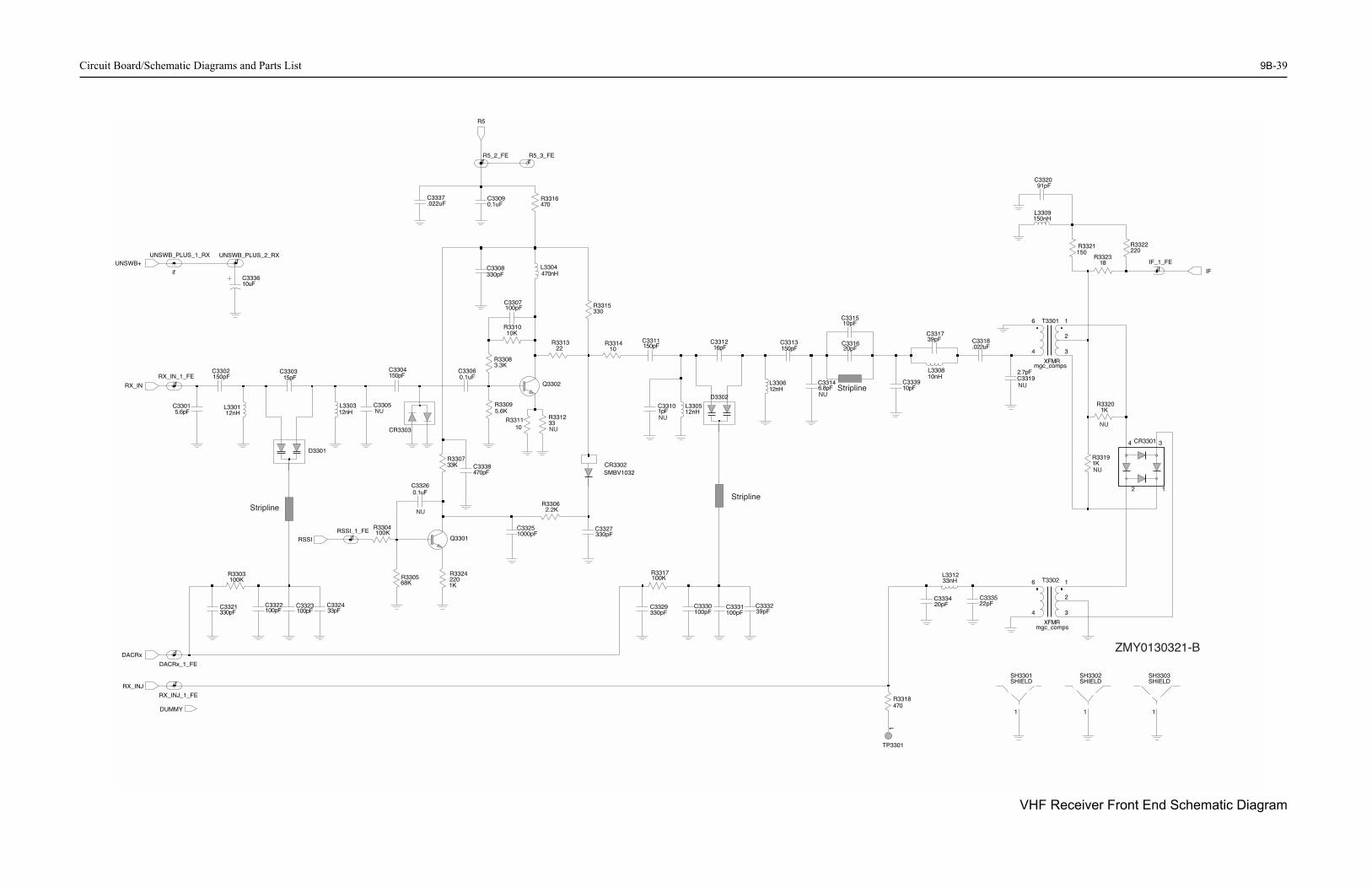
9B
-39
NU
NUStripline
NU
NU
6.8pFC3314
C331510pF
C331620pF
C331739pF
10nHL3308
10pFC3339
.022uFC3318
C33192.7pF
3
1
2
T3301
XFMR
4
6
mgc_comps
R33201K
1KR3319
2
34
1
CR3301
IFifIF_1_FE
L3309 150nH
150R3321 R3322
220
18R3323
C332091pF
C3334
XFMR
T3302
4
6
3
1
2
mgc_comps
C333522pF
33nHL3312
20pF
TP3301
1
11
SH3303SHIELD
1
SH3302SHIELD
SH3301SHIELD
R3318470
ZMY0130321-B
VHF Receiver Front End Schematic Diagram
Circuit Board/Schematic Diagrams and Parts List
NU
NU
NU
Stripline
NUStripline
UNSWB+
C333610uF
UNSWB_PLUS_1_RX
if
ifUNSWB_PLUS_2_RX
.022uFC3337 R3316
4700.1uFC3309
ifR5_2_FE
ifR5_3_FE
R5
470nHL3304
330pFC3308
0.1uFC3306
330R3315
Q3302
10KR3310
3.3KR3308
100pFC3307
22R3313
R331233R3311
10
5.6KR3309
C3304150pF
CR3303
C3305
470pFC3338
R330733K
1pFC3310
150pFC3311
10R3314
L330512nH
CR3302SMBV1032
16pFC3312
D3302
L330612nH
150pFC3313
C3331C3330100pF100pF330pF
C3329
100KR3317
C333239pF
2.2KR3306
1000pFC3325 C3327
330pFQ3301
0.1uFC3326
100KR3304
R33242201K68K
R3305
ifRSSI_1_FE
RSSI
D3301
150pFC3302
L330312nH
ifRX_IN_1_FE
L330112nH
15pFC3303
RX_IN
C33015.6pF
330pFC3321
33pFC3324
100pFC3322
100KR3303
C3323100pF
RX_INJ
ifDACRx
DACRx_1_FE
if
RX_INJ_1_FE
DUMMY

Circuit Board/Schematic Diagrams and Parts List
NU
275.9K
C32780.1uF
0pF
R32741K
C32791uF
CLK
LVZ
IF_S
EL
16.8
MH
z
DA
TA
2
F44
Vdd_FILTEREDd_FILTERED
C322010pF
R32204.7K
1uHL3221
C3228.01uF C3229
100pF .022uFC3239
C32260.1uF
C32250.1uF
0.15uFC3238
1uFC3232
1uFC3233C3234
1uFC32311uF
C32350.22uF
0.1uFC3224
100pFC3237
.01uFC32360.22uF
C3240R3224
10
R32231K
SQ_OUT_1_ZIFif
DEMOD_1_ZIFif
SQ_OUT
DEMOD
Vdd_FILTERED
Vdd_FILTERED
SHIELDSH3202
1
LVZIF_SEL_1_ZIFif
CLK_3_ZIF
DATA_3_ZIF
if
if
if16_8MHz_3_ZIF
0.1uFC3223.01uF
C3227
1200pFC3241
0.1uFC3242
SH3203SHIELD
1 2 3
NU
RSSI_FLT5 RSSI_OUT4
TE
ST
A16
TESTD8
VAG32
VAG_REF25
VPP9
PHASE_LOCK26
PR
EA
MP
_OU
T47
PR
E_A
GC
48
PRE_IN3
RED_VCC1
RED_VSS2
ROSE_VCC30
ROSE_VSS29
GO
LD_V
SS
14
GR
EE
N_V
CC
41
GR
EE
N_V
SS
43
15IO
UT
31LIM
42M
IX_B
YP
46M
IX_I
N
MLP
D_C
R2417
DA
TA
DEMOD_HF28
DEMOD_OUT27
EMIT11
EXTBS6
21F
RE
FG
ND
20
GOLD_VCC10
C2P
39
C3M35
C3P
38
C4M36C
4P37
19C
EX
18C
LK
CO
L13
BASE12
BLU
E_V
CC
45
BLU
E_V
SS
44
BR
OW
N_V
CC
22 23B
RP
_OF
F
C1M33
C1P
40
C2M34
mgc_compsU3220
AFC7
32D83
ZMY0130407-A
9B-40
(SOURCE)
NUNU
RSSI
R3206100K
R3208100
R320739K
0.1uFC3208
Q3201
XTALY3200
1KR3209
16pFC3200
IF_1_ZIF
C32011.5pF
L32001uH
IF OUT 3IN6G
ND
1
GN
D1
2
GN
D2
4
GN
D3
5 1uHL3201
12pFC3202
RSSI
R32112.2K
RSSI2.2K
R3213
if
RSSI_2_ZIFRSSI_1_ZIF
if
C32091uF
R5
R32012.2K
R3200150
C3204.01uF
C32050.1uF
if R5_3_ZIF
1000pFC3210
1uHL3202
C3203100pF
R32024.7K R3210
2.2K
R32124.7K
MMBR941Q3200
22R3204
10KR3203
.01uFC3206
1KR3205 C3207
2.2pF
.01uF
C3221C32184.7uF
C3230100pF
5V
VSFif
VSF_3_ZIF
C32140.1uF
1K
R3225
Q3202
5V_3_ZIF
if5V
R3217
104.7uFC3211
R3214100
SWB_PLUS_3_ZIF
ifR3215
100
10pFC3215
SWB+
1uF C3212
Vdd_FILTERED
R3218
GN
D
2
4NCON_OFF*3
VIN1
VOUT5
LP2980U3201
C32134.7uF
if
Vdda_3_ZIF
Vdda
Vdd_FILTERED
C3271330pF
.022uFC3270
10R3226
R327147
10pFC3273
C32724.7pF
Q3270BFQ67W
1
3
2
33pFC3274
100nHL3270R3273
47K
1KR3270 C3275
56pF
R327247K C3276
47pF 82pFC3277
2.2uHL3271 R3
3
C3288200R3276
200KD3270
SH3201
1
SHIELD
C32190.1uF
100R3219
Vdd_FILTERED
0.1uFC322
100KR3222
.022uFC3243
.01uC32
5V
Vd
R3221100
5V
VHF Receiver Back End Schematic Diagram

9B
-41
WARP
XTAL1XTAL2
TEST1TEST2
VMULT1VMULT2VMULT3VMULT4
SFOUT
MODOUTFREFOUT
IADAPT
INDMULT
IOUT
LOCK
AUX3AUX4
ADAPTSW
AUX1AUX2
VR
OV
CP
PR
E_V
DD
PD
_VD
D
DV
DD
AV
DD
VBPASSPVREF
REFSEL
SFBASESFCAP
SFIN
MODIN
NC1NC2NC3
PREIN
DATA
BIAS1BIAS2
CCOMP
CEXCLK
PR
E_G
ND
PD
_GN
D
DG
ND
AG
ND
3344 622
1347 34 536 20
2135
18
2726
30
10
172931
32
7
4039
42
98
U370163A27
uF711
2NR
4OUT
3SD
6ERR
1
GN
D
5IN
ADP3300U3711
SWB_PLUS_1_FN
2.2uFC3713
C37120.1uF
SWB+
C3735NU
R3763NU
GN
D3
IN1
OUT2
16.8MHz 45J49Y3761
D3761
R376147K
NUR3760
.01uFC3731C3763
2F
AD
J
4GND
3O
UT
1VDD
1.6pF
NU
OSC_16.8MHZ16.8MHz
Y3762
C3751NU
5V
C37332.2uF
2.2uHL3731
C3734.01uF.01uF
C3732
VddaVdda_1_FN
220pF220pFC3745C3742
220pFC3744 C3743
220pF
CSX_1_FN
DATA_1_FN
MODIN_1_FN
CLK_1_FN
CLK
MODIN
DATA
CSX
C3753C3752
4.7uF1000pF 0.1uF
C3754
VSF_1_FN
VSF
PRESC_1_FN
8.2pFC3726
PRESC
2.2uFC3755
200KR3751
R3752330K
R3727100K
100pFC3727
TP37021
7.5V
2.5V - 3.5V
RMS
4.55V
3.3V
ZMY0130322-D
VHF Synthesizer Schematic Diagram
Circuit Board/Schematic Diagrams and Parts List
25
2324
3738
15141211
28
4119
45
16
43
4
23
46
481
TRB_1_FN
LOCK
TRB
LOCK_1_FN
220pFC3746
BIAS_ADJ_1_FN
BIAS_ADJ
NUNU
C3725R3726
100R3701
2.2uFC3710
390nHL3701
0.1uFC3709R3703
150
C370722pF
NUR3702
C37080.1uF
33K
K11
K22
K33
R3705D3702
A16
A25
A34
R3704150
A2 5A3
4
1 K1
2 K2
3 K3
D3701
A16
C3703.01uF
C3704.01uF
.01uFC3701
.01uFC3702
0.1uFC3705
C37064.7uF
470R3721
100pFC3716
100pFC3715
4.7uFC3714
1uFC3724
R3723100
TP3701 1
0.1uFC3722
1KR3722
0.1uFC3721
4
1
3
Q3721
2
UMC5N
R5
5V
T5_1_FN
R5_2_FN
VCTRL_1_FN
R5_1_FN
T5
VCTRL
4.7K47K
47K
10K
5V_1_FN5V (SOURCE)
10C3
VCO_MOD_1_FN
VCO_MOD
11
SH3702SHIELD
SH3701SHIELD
16_8MHz_1_FN16.8MHz
100R3741
NUC3741
330pFC3762R3762
NU
56pFC3761
13.2V
R: 5VT: 0V
R: 0VT: 5V
3.5 - 9.5V@135-174MHz
RF mV RMS measured with high impedance probe.
5V
120mV RMS
400mV

Circuit Board/Schematic Diagrams and Parts List
47822
15pFC3836
6.8pF
VCO_MOD_1_VCO
6
L383156nH 56nH
L383356pFC3834
VCO_MOD
L383268nH
C3835
C38264.7pF
826
C382456pF
L382156nH
L382247nH
C382515pF
C383068pF
L382347nH
NUR3812
L38261uH
BIAS_ADJBIAS_ADJ_1_VCO
0.22uFC3827
23F
33KR3823R3824
22K
L38241uH
L3825100nH
VCTRL_1_VCO
VCTRL
C3828.01uF
100R3828
.01uFC3829
D3821
L38341uH
C38421000pF
D3831
R: 250mV RMS R: 1V RMS
R, T: 3.5V-9.5V@ 135MHz-174MHz
R:1.7VT: 0V
T: 1V RMSV RMS
ZMY0130406-A
9B-42
R380524K
10R3808 10K
R3804
0.1uF
RX_INJ_1_VCO
C3804
Q3801
C38014.7pF
R3801 C3802NU
100nH
RX_INJ
L3801
NU
100R3802
R3807NU
R5_1_VCO
R5
C3806100pF
R380622
L3811100nH
C3810NU
L3812100nH 0.1uF
C3812
R3811100
C38110.1uF
VSF_1_VCO
Vdda
R38170
L38131uH
Vdda_3_VCO
VSF
C3813.01uF
R3818NU
C3818.022uF
C38221000pF
220R3821
R3
C38054.7pF
C38031000pF
R3803220
27nHL3809C3809
27pF
C380815pF
1
SHIELDSH3802SHIELD
1
SHIELDSH3801SHIELD
TX_INJ_1_VCO
1KR3816
T5
VSFPRESC_1_VCO
T5_1_VCO
L3816100nH
6.8pFC3816
TX_INJ
NUR3830
PRESC
1000pFC3832
12KR3832
1000pFC3815
VSF
220R3833
TRB_1_VCOR38290
R383547K
TRB
47R3834
4.7pFC3833
10KR383
D3832
1R38R3825
33
10KR3831
C38.01u
C3821.01uF
VC
C_L
OG
IC
SUPER_FLTR
TRB_IN
TX_BASE
TX_EMITTER
TX_IADJTX_OUT
TX_SWITCH
VC
C_B
UF
FE
RS
GN
D_F
LAG
GN
D_L
OG
IC
PRESC_OUTRX_BASE
RX_EMITTER
RX_IADJRX_OUT
RX_SWITCH
COLL_RFIN
FLIP_IN
GN
D_B
UF
FE
RS
U380150U54
18
3
19
1615
110
13
14
917
12
56
28
7
4
20
11
R:4.6VT: 0V
R:4VT: 2.8V
3.3V 4.55V
T: 250m
R:0VT: 3.1V
3.1V
500mVRMS
R:0.9VT: 0V
800mVRMS
RF mV RMS measured with high impedance probe.
VHF Voltage Controlled Oscillator Schematic Diagram

9B
-43
L352223.75nH
C352810pF
C352522pF
NUC3527
130pFC3523
20pFC3524
.022uFC3526
1uHL3523
120R3573
D3521
R3572120
R3571NU
C3569.022uF
ANT_BIAS
NUR3569
R3570NU
NUQ3561
UNSWB+
SH3502SHIELD
12pFC3531
L353134.14nH
9.1pFC3533
C353230pF
34.14nHL3532
C353524pF
10pFC3534
C353615pF
18pFC3537
GND 4
1
2
3
RF_JACKJ3501
ANTENNA_CONTACTJ3502
30.54nHL3538
18pFC3539
RX_INRX_IN_1_PA
C355256pF
91pFC3551
39R3551
7.66nHL3552
D355120pF
C3550
43.67nHL3551
0985613Z01
21
501
K1K2K3
CR3501
A1A2A3
ZMY0130323-D
VHF Transmitter Schematic Diagram
Circuit Board/Schematic Diagrams and Parts List
VG
6V
L19
VLI
M
2T
1
30TEMP
14V10
16V45V
5EX
T17
VA
R1
20
VA
R2
18
VA
R3
24
15
INT
NA
22
11Q
QX10
RF
IN1
21R
S
RSET31
23R
X
7C
L
26CLK
12CQ
CQX1328
DATA
9F168
GN
D1
8
GND225
4
32 ANO
BPOS27
29CEX
CI
3 5C
J
H99S-4U3502
C35601uF
3300pFC3562
330KR3564
R3565NU
C3565.022uF
C35633300pF
220pFC3564
1uFC3516
330pFC3567
C3519
C3518R3513
L3518
L351513.85nH
R35190.1
3300pFC3515
Microstrip
D
G
S
Q3501
7.66nHL3521
220pFC3521
UNSWB+UNSWB+
330pFC3570
5V_2_PARESET_1_PA
5VRESET
BIAS_TUNING
CLKUNSWB+ DATACSX
DATA_2_PA
CLK_2_PA
UNSWB_LPLUS_2_PA
CSX_2_PA
UNSW_LPLUS_3_PA
33KR3562
12KR3561
C3561.022uF
POS
VO
UT
2
U3503
GND3
100pFC3566 LM50C
5185963A15
L350468nH
270KR3563
C3508.022uF 330pF
C3509.022uF 68nH
L3503C3504
5.6nHL3501
C350333pF
C350233pF
18nHL3511
NUC3507C3506
NUNU
L3502
47pFC3512
R3541NU330pF
C3542
L351211.03nH
C351330pF
C3541.022uF BIAS_TUNING
TP3502
1
12KR3547
.022uFC3547
100R3544
100R3545
R354633K
C3546330pF
R35487.5K
H3501
1
HEATSINK
SHIELDSH3501
C3544330pF
100R3543
.022uFC3543
5.6KR3542
C3505330pF
6
7RFOUT21 VCNTRL14 VD1 2VG1
3VG2
GN
D3
12
GN
D4
13
8 NC19 NC2
10 NC315 NC4
16 RFIN RFOUT1
U3501
11 G2
GN
D1
4
GN
D2
5
C65
R3505470
R3503300
330pFC3501
300R3501
TX_INJ_1_PATX_INJ
18R3502
BEADL3519 C3568
3300pF
1
17E
P
R3512NU
R35063.9
R35073.9
L35137.66nH
C351468pF
68pFC3517
NU
NU
NU
NU
VR310V

Circuit Board/Schematic Diagrams and Parts List
330pF47pF30pF68pF3300pF1uF
220pF130pF20pF22pF22000pF, +80%/-20%GCAM Dummy Part Number10pF12pF30pF9.1pF10pF24pF15pF20pF18pF22000pF, +80%/-20%330pF22000pF, +80%/-20%330pF330pF22000pF, +80%/-20%20pF91pF56pF1uF22000pF, +80%/-20%3300pF3300pF220pF0.022uF100pF330pF3300pF22000pF, +80%/-20%330pF10000pF, 10%10000pF, 10%10000pF, 10%10000pF, 10%0.1uF4.7uF22pF100000pF, +80%/-20%
Description
C3709 2113743M24 100000pF, +80%/-20%C3710 2104993J02 2.2uFC3711 2311049A69 10uF, 20%C3712 2113743M24 100000pF, +80%/-20%C3713 2311049A09 2.2uFC3714 2311049J11 4.7uFC3715 2113743N50 100pFC3716 2113743N50 100pFC3721 2113743E20 0.1uFC3722 2113743E20 0.1uFC3724 2311049A08 1uFC3725 Not PlacedC3726 2113743N24 8.2pFC3727 2113743N50 100pFC3731 2113743L41 10000pF, 10%C3732 2113743L41 10000pF, 10%C3733 2104993J02 2.2uFC3734 2113743L41 10000pF, 10%C3735 Not PlacedC3741 Not PlacedC3742 2113743L01 220pFC3743 2113743L01 220pFC3744 2113743L01 220pFC3745 2113743L01 220pFC3746 2113743L01 220pFC3751 Not PlacedC3752 2113743L17 1000pFC3753 2311049A56 4.7uFC3754 2113743M24 100000pF, +80%/-20%C3755 2104993J02 2.2uFC3761 2113743N44 56pFC3762 2113740F63 330pFC3763 2113743N08 1.6pFC3801 2113743N18 4.7pFC3802 Not PlacedC3803 2113743L17 1000pFC3804 2113743E20 0.1uFC3805 2113743N18 4.7pFC3806 2113743N50 100pFC3808 2113743N30 15pFC3809 2113743N36 27pFC3810 Not PlacedC3811 2113743M24 100000pF, +80%/-20%C3812 2113743M24 100000pF, +80%/-20%C3813 2113743L41 10000pF, 10%C3815 2113743L17 1000pFC3816 2113743N22 6.8pFC3818 2113743E07 0.022uFC3821 2113743L41 10000pF, 10%C3822 2113743L17 1000pFC3823 2113743L41 10000pF, 10%
Circuit Ref
Motorola Part No.
Description
9B-44
VHF Radio Parts List
Circuit Ref
Motorola Part No.
Description
B501 0986237A02 Battery ContactC3200 2113743N31 16pFC3201 Not PlacedC3202 Not PlacedC3203 2113743N50 100pFC3204 2113743L41 10000pF, 10%C3205 2113928N01 0.1uFC3206 2113743L41 10000pF, 10%C3207 2113743N10 2.2pFC3208 Not PlacedC3209 2311049A07 1uFC3210 2113743L17 1000pFC3211 2311049A56 4.7uFC3212 2311049A07 1uFC3213 2311049A56 4.7uFC3214 2113928N01 0.1uFC3215 2113743N26 10pFC3218 2311049A56 4.7uFC3219 2113928N01 0.1uFC3220 2113743N26 10pFC3221 2113743L41 10000pF, 10%C3222 2113928N01 0.1uFC3223 2113928N01 0.1uFC3224 2113928N01 0.1uFC3225 2113928N01 0.1uFC3226 2113928N01 0.1uFC3227 2113743L41 10000pF, 10%C3228 2113743L41 10000pF, 10%C3229 2113743N50 100pFC3230 2113740F51 100pFC3231 2180478Z20 1uFC3232 2180478Z20 1uFC3233 2180478Z20 1uFC3234 2180478Z20 1uFC3235 2113743A23 0.22uFC3236 Not PlacedC3237 Not PlacedC3238 2113743A24 0.33uFC3239 2113743E07 0.022uFC3240 2113743A23 0.22uFC3241 2113743L19 1200pFC3242 2109720D14 0.1uF, 1206C3243 2113743E07 0.022uFC3244 2113743L41 10000pF, 10%C3270 2113743E07 0.022uFC3271 2113743L05 330pFC3272 2113743N18 4.7pFC3273 2113743N26 10pFC3274 2113743N38 33pF
C3275 2113743N44 56pFC3276 2113743N42 47pFC3277 2113743N48 82pFC3278 2113743E20 0.1uFC3279 2311049A07 1uFC3280 2113743L39 8200pFC3301 2113743N29 13pFC3302 2113743N54 150pFC3303 2113743N33 20pFC3304 2113743N54 150pFC3305 Not PlacedC3306 2113928N01 0.1uFC3307 2113743N50 100pFC3308 2113743L05 330pFC3309 2113928N01 0.1uFC3310 Not PlacedC3311 2113743N54 150pFC3312 2113743N31 16pFC3313 2113743N54 150pFC3314 Not PlacedC3315 2113743N26 10pFC3316 2113743N33 20pFC3317 2113743N40 39pFC3318 2113743M08 22000pF, +80%/-20%C3319 Not PlacedC3320 2113743N49 91pFC3321 2113743L05 330pFC3322 2113743N50 100pFC3323 2113743N50 100pFC3324 2113743N38 33pFC3325 2113743L17 1000pFC3326 Not PlacedC3327 2113743L05 330pFC3329 2113743L05 330pFC3330 2113743N50 100pFC3331 2113743N50 100pFC3332 2113743N40 39pFC3334 2113743N33 20pFC3335 2113743N34 22pFC3336 2311049A18 10uFC3337 2113743M08 22000pF, +80%/-20%C3338 2113743L09 470pFC3339 2113743N26 10pFC3501 2113743L05 330pFC3502 2113743N38 33pFC3503 2113743N38 33pFC3504 2113743M08 22000pF, +80%/-20%C3505 2113743N38 33pFC3506 Not PlacedC3507 Not PlacedC3508 2113743M08 22000pF, +80%/-20%
Circuit Ref
Motorola Part No.
Description
C3509 2113743L05C3512 2113740F43C3513 2113740F38C3514 2113740F47C3515 2113743L29C3516 2311049A08C3518 Not PlacedC3519 Not PlacedC3521 2111078B51C3523 2111078B45C3524 2113740F34C3525 2113740F35C3526 2113743M08C3527 Not PlacedC3528 2113740F27C3531 2113740F29C3532 2113740F38C3533 2113740F26C3534 2113740F27C3535 2113740F36C3536 2113740F31C3537 2113740F34C3539 2113740F33C3541 2113743M08C3542 2113743L05C3543 2113743M08C3544 2113743L05C3546 2113743L05C3547 2113743M08C3550 2113743N33C3551 2113743N49C3552 2113743N44C3560 2311049A07C3561 2113743M08C3562 2113743L29C3563 2113743L29C3564 2113743L01C3565 2113743E07C3566 2113743N50C3567 2113743L05C3568 2113743L29C3569 2113743M08C3570 2113743L05C3701 2113743L41C3702 2113743L41C3703 2113743L41C3704 2113743L41C3705 2113743E20C3706 2311049J11C3707 2113743N34C3708 2113743M24
Circuit Ref
Motorola Part No.
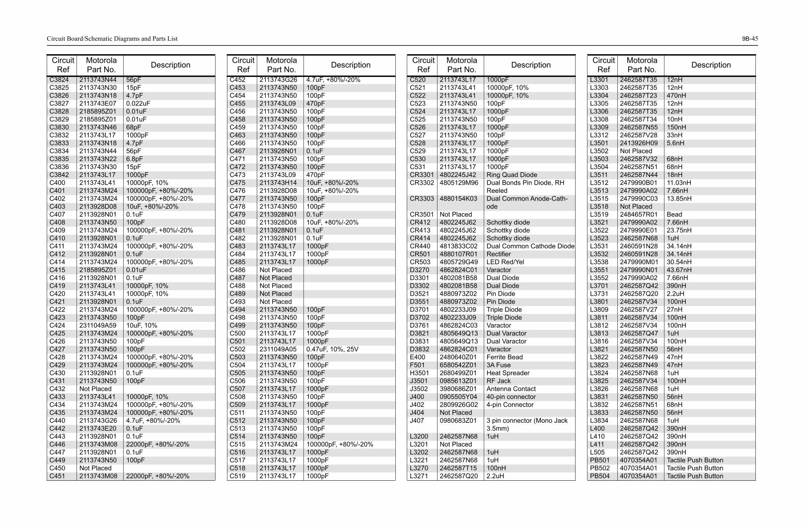
9B
-45
1000pF10000pF, 10%10000pF, 10%
0 100pF1000pF
0 100pF1000pF
0 100pF1000pF1000pF1000pF1000pFRing Quad Diode
6 Dual Bonds Pin Diode, RH Reeled
3 Dual Common Anode-Cath-ode
Schottky diodeSchottky diodeSchottky diode
2 Dual Common Cathode Diode1 Rectifier9 LED Red/Yel1 Varactor8 Dual Diode8 Dual Diode2 Pin Diode2 Pin Diode
Triple DiodeTriple Diode
3 Varactor 3 Dual Varactor3 Dual Varactor1 Varactor1 Ferrite Bead1 3A Fuse1 Heat Spreader1 RF Jack1 Antenna Contact4 40-pin connector2 4-pin Connector
1 3 pin connector (Mono Jack 3.5mm)
8 1uH
8 1uH8 1uH5 100nH0 2.2uH
.
Description
L3301 2462587T35 12nHL3303 2462587T35 12nHL3304 2462587T23 470nHL3305 2462587T35 12nHL3306 2462587T35 12nHL3308 2462587T34 10nHL3309 2462587N55 150nHL3312 2462587V28 33nHL3501 2413926H09 5.6nHL3502 Not PlacedL3503 2462587V32 68nHL3504 2462587N51 68nHL3511 2462587N44 18nHL3512 2479990B01 11.03nHL3513 2479990A02 7.66nHL3515 2479990C03 13.85nHL3518 Not PlacedL3519 2484657R01 BeadL3521 2479990A02 7.66nHL3522 2479990E01 23.75nHL3523 2462587N68 1uHL3531 2460591N28 34.14nHL3532 2460591N28 34.14nHL3538 2479990M01 30.54nHL3551 2479990N01 43.67nHL3552 2479990A02 7.66nHL3701 2462587Q42 390nHL3731 2462587Q20 2.2uHL3801 2462587V34 100nHL3809 2462587V27 27nHL3811 2462587V34 100nHL3812 2462587V34 100nHL3813 2462587Q47 1uHL3816 2462587V34 100nHL3821 2462587N50 56nHL3822 2462587N49 47nHL3823 2462587N49 47nHL3824 2462587N68 1uHL3825 2462587V34 100nHL3826 2462587N68 1uHL3831 2462587N50 56nHL3832 2462587N51 68nHL3833 2462587N50 56nHL3834 2462587N68 1uHL400 2462587Q42 390nHL410 2462587Q42 390nHL411 2462587Q42 390nHL505 2462587Q42 390nHPB501 4070354A01 Tactile Push ButtonPB502 4070354A01 Tactile Push ButtonPB504 4070354A01 Tactile Push Button
Circuit Ref
Motorola Part No.
Description
Circuit Board/Schematic Diagrams and Parts List
C3824 2113743N44 56pFC3825 2113743N30 15pFC3826 2113743N18 4.7pFC3827 2113743E07 0.022uFC3828 2185895Z01 0.01uFC3829 2185895Z01 0.01uFC3830 2113743N46 68pFC3832 2113743L17 1000pFC3833 2113743N18 4.7pFC3834 2113743N44 56pFC3835 2113743N22 6.8pFC3836 2113743N30 15pFC3842 2113743L17 1000pFC400 2113743L41 10000pF, 10%C401 2113743M24 100000pF, +80%/-20%C402 2113743M24 100000pF, +80%/-20%C403 2113928D08 10uF, +80%/-20%C407 2113928N01 0.1uFC408 2113743N50 100pFC409 2113743M24 100000pF, +80%/-20%C410 2113928N01 0.1uFC411 2113743M24 100000pF, +80%/-20%C412 2113928N01 0.1uFC414 2113743M24 100000pF, +80%/-20%C415 2185895Z01 0.01uFC416 2113928N01 0.1uFC419 2113743L41 10000pF, 10%C420 2113743L41 10000pF, 10%C421 2113928N01 0.1uFC422 2113743M24 100000pF, +80%/-20%C423 2113743N50 100pFC424 2311049A59 10uF, 10%C425 2113743M24 100000pF, +80%/-20%C426 2113743N50 100pFC427 2113743N50 100pFC428 2113743M24 100000pF, +80%/-20%C429 2113743M24 100000pF, +80%/-20%C430 2113928N01 0.1uFC431 2113743N50 100pFC432 Not PlacedC433 2113743L41 10000pF, 10%C434 2113743M24 100000pF, +80%/-20%C435 2113743M24 100000pF, +80%/-20%C440 2113743G26 4.7uF, +80%/-20%C442 2113743E20 0.1uFC443 2113928N01 0.1uFC446 2113743M08 22000pF, +80%/-20%C447 2113928N01 0.1uFC449 2113743N50 100pFC450 Not PlacedC451 2113743M08 22000pF, +80%/-20%
Circuit Ref
Motorola Part No.
Description
C452 2113743G26 4.7uF, +80%/-20%C453 2113743N50 100pFC454 2113743N50 100pFC455 2113743L09 470pFC456 2113743N50 100pFC458 2113743N50 100pFC459 2113743N50 100pFC463 2113743N50 100pFC466 2113743N50 100pFC467 2113928N01 0.1uFC471 2113743N50 100pFC472 2113743N50 100pFC473 2113743L09 470pFC475 2113743H14 10uF, +80%/-20%C476 2113928D08 10uF, +80%/-20%C477 2113743N50 100pFC478 2113743N50 100pFC479 2113928N01 0.1uFC480 2113928D08 10uF, +80%/-20%C481 2113928N01 0.1uFC482 2113928N01 0.1uFC483 2113743L17 1000pFC484 2113743L17 1000pFC485 2113743L17 1000pFC486 Not PlacedC487 Not PlacedC488 Not PlacedC489 Not PlacedC493 Not PlacedC494 2113743N50 100pFC498 2113743N50 100pFC499 2113743N50 100pFC500 2113743L17 1000pFC501 2113743L17 1000pFC502 2311049A05 0.47uF, 10%, 25VC503 2113743N50 100pFC504 2113743L17 1000pFC505 2113743N50 100pFC506 2113743N50 100pFC507 2113743L17 1000pFC508 2113743N50 100pFC509 2113743L17 1000pFC511 2113743N50 100pFC512 2113743N50 100pFC513 2113743N50 100pFC514 2113743N50 100pFC515 2113743M24 100000pF, +80%/-20%C516 2113743L17 1000pFC517 2113743L17 1000pFC518 2113743L17 1000pFC519 2113743L17 1000pF
Circuit Ref
Motorola Part No.
Description
C520 2113743L17C521 2113743L41C522 2113743L41C523 2113743N5C524 2113743L17C525 2113743N5C526 2113743L17C527 2113743N5C528 2113743L17C529 2113743L17C530 2113743L17C531 2113743L17CR3301 4802245J42CR3302 4805129M9
CR3303 4880154K0
CR3501 Not PlacedCR412 4802245J62CR413 4802245J62CR414 4802245J62CR440 4813833C0CR501 4880107R0CR503 4805729G4D3270 4862824C0D3301 4802081B5D3302 4802081B5D3521 4880973Z0D3551 4880973Z0D3701 4802233J09D3702 4802233J09D3761 4862824C0D3821 4805649Q1D3831 4805649Q1D3832 4862824C0E400 2480640Z0F501 6580542Z0H3501 2680499Z0J3501 0985613Z0J3502 3980686Z0J400 0905505Y0J402 2809926G0J404 Not PlacedJ407 0980683Z0
L3200 2462587N6L3201 Not PlacedL3202 2462587N6L3221 2462587N6L3270 2462587T1L3271 2462587Q2
Circuit Ref
MotorolaPart No

Circuit Board/Schematic Diagrams and Parts List
120120100
15015033K4701000100
100K 100200K330K
47K
10022010K 24K 22
10100
10000
2204733K22K33181000
10K 12K2204747K 10K 47K
Description
R401 0662057M01 0R402 Not PlacedR403 Not PlacedR405 0662057M01 0R406 0662057N20 75KR408 Not PlacedR410 0662057N23 100K R411 0662057M98 10K R413 0662057M01 0R414 0662057V34 180KR415 0662057V26 91KR416 0662057M98 10K R418 0662057M01 0R419 0662057M90 4700R423 0662057N39 470KR425 0662057N10 30KR427 0662057M98 10K R428 0662057M10 2.2R429 0662057M98 10K R432 0662057N16 51KR434 Not PlacedR435 0662057M81 2000R436 0662057N15 47K R437 Not PlacedR438 0662057M01 0R439 0662057N23 100K R445 0662057N08 24K R446 Not PlacedR447 0662057N23 100K R448 0662057M98 10K R449 0662057N08 24K R451 0662057N03 15KR452 0662057N23 100K R454 Not PlacedR455 Not PlacedR456 0662057M01 0R457 0662057M98 10K R460 0662057M90 4700R461 0662057N23 100K R462 0662057N23 100K R463 0662057M61 300R467 0662057M98 10K R471 0662057N06 20KR472 0662057N12 36K R473 0662057M26 10R475 0662057M01 0R476 0662057N08 24K R478 0662057M98 10K
5480678Z01 Barcode LabelR492 0662057M01 0R493 Not Placed
Circuit Ref
Motorola Part No.
Description
9B-46
Q3200 4813827A07 NPN TransistorQ3201 4880214G02 NPN TransistorQ3202 4880214G02 NPN TransistorQ3270 4805218N63 RF TransistorQ3301 4880214G02 NPN TransistorQ3302 4813827A07 NPN TransistorQ3501 4813828A08 RF Power FETQ3561 Not PlacedQ3721 4802245J50 Dual NPN/PNP TransistorQ3801 4813827A07 NPN TransistorQ400 4809579E18 MOSFET P-ChannelQ403 4813824A17 PNP TransistorQ405 4802245J54 Dual NPN TransistorQ410 4802245J54 Dual NPN TransistorQ417 4802245J50 Dual NPN/PNP TransistorQ418 4802245J50 Dual NPN/PNP TransistorQ419 5180159R01 Dual NPN TransistorQ420 4805128M67 PNP TransistorQ421 4880214G02 NPN TransistorQ431 5180159R01 Dual NPN TransistorQ433 4880214G02 NPN TransistorQ502 5180159R01 Dual NPN TransistorQ505 4880214G02 NPN TransistorQ506 4802245J50 Dual NPN/PNP TransistorR3200 0662057M54 150R3201 0662057M82 2200R3202 0662057M90 4700R3203 0662057M98 10K R3204 0662057M34 22R3205 0662057M74 1000R3206 0662057N23 100K R3207 0662057N13 39K R3208 0662057M50 100R3209 0662057M74 1000R3210 0662057M82 2200R3211 0662057M82 2200R3212 0662057M90 4700R3213 0662057M82 2200R3214 0662057M50 100R3215 0662057M50 100R3217 Not PlacedR3218 Not PlacedR3219 0662057M50 100R3220 0662057M90 4700R3221 0662057M50 100R3222 Not PlacedR3223 Not PlacedR3224 0662057M26 10R3225 0662057M74 1000R3226 0662057M26 10R3270 0662057M74 1000
Circuit Ref
Motorola Part No.
Description
R3271 0662057M42 47R3272 0662057N15 47K R3273 0662057N15 47K R3274 0662057M74 1000R3275 0662057M88 3900R3276 0662057N30 200KR3303 0662057N23 100K R3304 0662057N23 100K R3305 0662057N19 68K R3306 0662057M82 2200R3307 0662057N11 33KR3308 0662057M86 3300R3309 0662057M92 5600R3310 0662057M98 10K R3311 0662057M26 10R3312 Not PlacedR3313 0662057M34 22R3314 0662057M26 10R3315 0662057M62 330R3316 0662057M61 300R3317 0662057N23 100K R3318 0662057M66 470R3319 Not PlacedR3320 Not PlacedR3321 0662057M54 150R3322 0662057M58 220R3323 0662057M32 18R3324 0662057M58 220R3501 0662057M61 300R3502 0662057M32 18R3503 0662057M61 300R3505 0662057M62 330R3506 0662057B62 3.9R3507 0662057B62 3.9R3512 Not PlacedR3513 Not PlacedR3519 0680539Z01 0.1R3541 0662057N13 39K R3542 0662057M92 5600R3543 0662057M50 100R3544 0662057A25 100R3545 0662057A25 100R3546 0662057N01 12KR3547 0662057N11 33KR3548 0662057N07 22KR3551 0662057M40 39R3561 0662057N01 12KR3562 0662057N11 33KR3563 0662057N33 270K R3564 0662057N35 330KR3565 Not Placed
Circuit Ref
Motorola Part No.
Description
R3569 Not PlacedR3570 Not PlacedR3571 Not PlacedR3572 0662057A27R3573 0662057A27R3701 0662057M50R3702 Not PlacedR3703 0662057M54R3704 0662057M54R3705 0662057N11R3721 0662057M66R3722 0662057M74R3723 0662057M50R3726 Not PlacedR3727 0662057N23R3741 0662057M50R3751 0662057N30R3752 0662057N35R3760 Not PlacedR3761 0662057N15R3762 Not PlacedR3763 Not PlacedR3801 Not PlacedR3802 0662057M50R3803 0662057M58R3804 0662057M98R3805 0662057N08R3806 0662057M34R3807 Not PlacedR3808 0662057M26R3811 0662057M50R3812 Not PlacedR3816 0662057M74R3817 0662057M01R3818 Not PlacedR3821 0662057M58R3822 0662057M42R3823 0662057N11R3824 0662057N07R3825 0662057M38R3826 0662057M32R3828 0662057M50R3829 0662057M01R3830 Not PlacedR3831 0662057M98R3832 0662057N01R3833 0662057M58R3834 0662057M42R3835 0662057N15R3836 0662057M98R400 0662057N15
Circuit Ref
Motorola Part No.

9B-47
Circuit Board/Schematic Diagrams and Parts List* Motorola Depot Servicing only
R494 0662057M01 0R495 0662057N23 100K R496 0662057N23 100K R498 0662057N23 100K R499 0662057M98 10K R501 0662057M70 680R502 0662057M56 180R505 0662057M98 10K R506 0662057N15 47K R507 0662057M01 0R510 0662057M98 10K RT400 0680590Z01 Thermistor 33KS501 4080710Z01 Channel SwitchS502 1880619Z02 Volume SwitchSH3201 2602023X08 Rx Back end top shieldSH3202 2686081B02 LVZIF ShieldSH3203 2686081B03 45.1MHz Xtal ShieldSH3301 2686081B01 Rx Back end bottom shieldSH3302 2686081B05 Mixer ShieldSH3303 2686081B06 Rx Front end top shieldSH3501 2680687Z01 Shield, Harmonic FilterSH3502 2686081B04 PA driver ShieldSH3701 2680511Z01 Synthesizer Top ShieldSH3702 2680511Z01 Synthesizer Bottom ShieldSH3801 2680513Z01 Shield, VCO TopSH3802 2680514Z01 Shield, VCO BottomSH400 2680505Z01 Controller Memory ShieldSH401 2680506Z01 On/off Controller ShieldSH402 2680515Z01 Microprocessor ShieldSH403 2680516Z01 ASFIC CMP/Audio PA Con-
troller ShieldT3301 2580541Z01 XFMR CoilT3302 2580541Z01 XFMR CoilU3201 5102463J58 3.3V Voltage RegulatorU3220 5109632D83 LVZIF ICU3501 5185130C65 LDMOS Driver ICU3502 5185765B28 Power Control ICU3503 5185963A15 Temperature SenseU3701 5185963A27 LVFRACN Synthesizer ICU3711 5105739X05 5V RegulatorU3801 5105750U54 VCO Buffer ICU400 5102463J40 3.3V Voltage RegulatorU404 5185130C53 ASFIC_CMPU405 Not PlacedU406 *5102463J59 FLASH ROM 128K X 8U407 *5102463J64 16K X 8 EEPROMU409 5102226J56 MicroprocessorU410 5102463J57 3.3V Voltage RegulatorU420 5102463J44 Audio PAVR3501 4880140L15 Zener Diode, 10VVR431 4802245J73 Zener Diode, 6.8V
Circuit Ref
Motorola Part No.
Description
VR432 4880140L15 Zener Diode, 10VVR433 4880140L15 Zener Diode, 10VVR439 4880140L15 Zener Diode, 10VVR440 4802245J73 Zener Diode, 6.8VVR441 4802245J73 Zener Diode, 6.8VVR444 4802245J73 Zener Diode, 6.8VVR450 4802245J75 Zener Diode, 12.0VVR451 4802245J74 Zener Diode, 10.0VVR501 4813830A18 Zener Diode, 6.8VVR506 4802245J73 Zener Diode, 6.8VY3200 4802245J43 Xtal FilterY3761 4805875Z04 16.8MHz Crystal OscillatorY3762 Not Placed
5480678Z01 Barcode Label8480675Z04 VHF main PC Board
Circuit Ref
Motorola Part No.
Description

Circuit Board/Schematic Diagrams and Parts List
K
9B-48
THIS PAGE INTENTIONALLY LEFT BLAN

Troubleshooting Charts 9B-49
10.0 Troubleshooting Charts
MCU Check
Power Up Alert Tone
OK?
SpeakerOK?
U409 EXTAL= 7.3728 MHz?
U201 Pin 19 16.8 MHz
5V at U247?3.3V at U248?
U409 Reset Pin 94 High?
MCU is OK
Not able to pro-gram RF Board
ICs
Before replacing MCU, check SPI clock, SPI data, and RF IC select
Replace Speaker
Read Radio OK?
Check Setup
Reprogram the correct data.
See FGU Troubleshooting
chart
7.5V at Pin 3/5 U247? 4/3.3V at Pin 1
U248
Check Q400
Replace U247/U248
Check any short to SWB+,
Vdda or Vddd
Press PTT. Red LED does not
light up
PTT U409 Pin 53 low?
Press PTT Q502-2 High?
Check PB504
Check Q502-2 voltage
LED Q502,R501
OK?
Replace Faulty
Component
Radio could not PTT
externally
U409 Pin 52 & 6
low?
See FGU Troubleshoot-
ing chart
LED should light up
Check MCU
PTT
NO
YES
YES
No
No
YES YES
NO
YES
YES
NO
NO
YES
YES
NO
NO
YES
NO
YES
NO
YES
YES
NO
NO
YES
EXTSPKR
EXTPTT
INTAUDIO
J402 Pin 3 low? Pin 4 high?
ASFIC U404 Pin 14 & 15
high?
Check Accessories
Check U404
Check U420 Audio PA
NO
NO
YES
YES
J402 Audio at Pin 3 &
Pin 4
Check Spk. Flex Connection
Audio at AudioPA
(U420) input (U447)
Audio from Pin 41 ASFIC, U404?
Check ASFIC U404
Check Audio PA
(U420)
Check U301
LV ZIF
Audio at Pin 2
U404?
NO
NO
NO
YES
YES
NO
YES
Troubleshooting Flow Chart for Controller
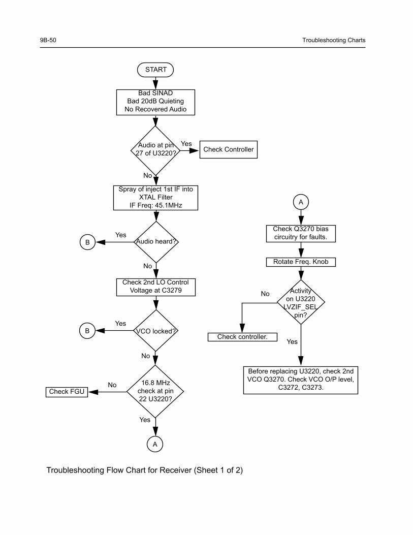
9B-50 Troubleshooting Charts
Bad SINADBad 20dB Quieting
No Recovered Audio
START
Audio at pin 27 of U3220? Check Controller
Yes
No
Spray of inject 1st IF into XTAL Filter
IF Freq: 45.1MHz
Audio heard?BYes
No
Check 2nd LO Control Voltage at C3279
VCO locked?BYes
16.8 MHz check at pin 22 U3220?
Activityon U3220
LVZIF_SEL pin?
Check FGU
No
No
A
A
Yes
Check Q3270 bias circuitry for faults.
Rotate Freq. Knob
Check controller.
Before replacing U3220, check 2nd VCO Q3270. Check VCO O/P level,
C3272, C3273.
Yes
No
Troubleshooting Flow Chart for Receiver (Sheet 1 of 2)

Troubleshooting Charts 9B-51
IF Signal at C3200?
No
RF Signal at T3301?
RF Signal atR3313?
No
RF Signal at C3306?
No
RF Signal at C3302?
No or
Check harmonic filter L3531 & L3532, C3532 and ant. switches D3521,
D3551, L3551, R3551, C3551, C3552, L3552
Check filter between C3302 & C3306; pro-
gram filter to schematic test freq and check var-
actor voltages.
Inject RF into J3501
Are varactor voltages OK?
No
Yes
Check RF amp (Q3302) Stage.
Check filter between C3313 & T3301.
Yes
Check T3301, T3302, CR3301, R3321, R3322,
R3323Yes
1st LO O/P OK?
Locked?
Yes
Check FGU
Yes
Trace IF signal from C3200 to
Q3200. Check for bad XTAL filter.
No
Yes Q3200 collec-tor OK?IF signal present? Before replacing
U3220, check U3220 volt-
ages; trace IF signal path.
Yes
Check for 2.9 VDC
Is R5 present?
Check Q3721, U3701 (pin 48) volt-
ages and U3711
No
No
No
Check U404 voltage and if U404 can be selected by
MCU before replacing U404.
Check varactor filter.
No
Yes
Yes
Yes
A
A
B
weak RF
Troubleshooting Flow Chart for Receiver (Sheet 2 of 2)

9B-52 Troubleshooting Charts
START
No Power
Is ThereB+ Bias for Ant switch
D3521
Check Q3561
Is Current OK?
IsControl Voltage High or
Low at TP3502Check PCIC
1. Check Pin Diodes2. Check Harmonic Filter
Inspect/Repair Tx. Output Network
Is Power OK?
Done
Check Drive to Module
Is Drive OK? Troubleshoot
VCO
Inspect PA Network/Check Power Out of U3501 at Cap C3512
Is Power OK?
Replace U3501
Is Power OK?
Replace Q3501
Done
Done
No
Yes
Yes No
No
Yes
Low
High
No
Yes
Yes
No
Yes
No
Troubleshooting Flow Chart for Transmitter

Troubleshooting Charts 9B-53
5V at pin 6 of
D3701
Is informationfrom µP U409
correct?
Is U3701 Pin 18 at
4.54 VDC?
Is U3701 Pin 47 13 VDC
Is U3701 Pin 19<0.7 VDC in RX &>4.3 VDC in TX?
Start
Visual check of the Board OK?
CorrectProblem
Check 5VRegulator
+5V at U3701Pin’s
13 & 30?
Is 16.8MHzSignal at
U3701 Pin 19?
Check Y3761, C3761, C3762, C3763, D3761
& R3761
Are signalsat Pin’s 14 &15 of U3701?
Check L3701, R3701
Check R3829
U3701 pin 2 at >3V in Tx and <0.7V in Rx
RemoveShorts
Is there a shortbetween Pin 47 and
Pins 14 & 15 ofU3701?
Replace orresolder
necessarycomponents
Is RF level atU3701 Pin 32
>-30 dBm?
Are C3721, C3722,C3724,R3721, R3722,
R3723 OK?
Replace U3701
If R3727, C3726 & C3727are OK, then see VCOtroubleshooting chart
Are Waveformsat Pins 14 & 15
triangular?
Do Pins 7,8 & 9of U3701 togglewhen channel is
changed?
Check programminglines between U409
and U3701 Pins 7,8 & 9
Replace U3701
Check uP U409Troubleshooting
Chart
NO
YES
NO
YES
NO
YES
NO
YES
NO
NO
NO
YES
YES
NO
YES
YES
NO
YES
YES
YESNO
NO
NO
NO
YES
NO
YES
YES
Check D3701, D3702, U3701, C3701 -
C3707
3.3V at U3701 pins 5, 20, 34 &
36
Check U3201, L3731
Is 16.8MHz signal at
U3701 pin 23?
Replace U3701
YES
NO
NO
YES
NO
YES
Troubleshooting Flow Chart for Synthesizer
Replace U3701
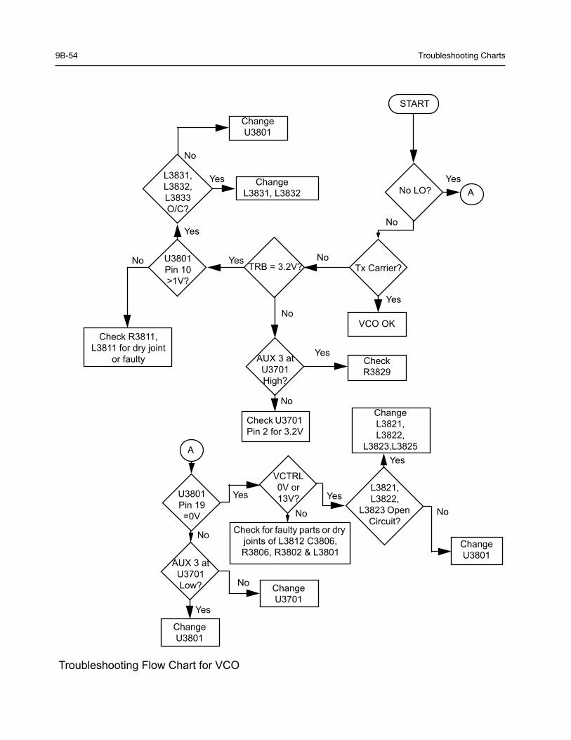
9B-54 Troubleshooting Charts
START
No LO?
Tx Carrier?
VCO OK
Check R3829
TRB = 3.2V?U3801Pin 10 >1V?
L3831, L3832, L3833O/C?
Change L3831, L3832
Change U3801
AUX 3 at U3701 High?
Check U3701 Pin 2 for 3.2V
U3801Pin 19 =0V
AUX 3 at U3701 Low?
Change U3801
VCTRL 0V or 13V?
L3821, L3822,
L3823 Open Circuit?
Change U3801
Change L3821, L3822,
L3823,L3825
Change U3701
Check for faulty parts or dry joints of L3812 C3806, R3806, R3802 & L3801
A
A
No
No
Yes
Yes
Yes
No
No
Yes
Yes
Yes
No
Yes
No
No
Yes
Yes
No
No
Check R3811, L3811 for dry joint
or faulty
No
Troubleshooting Flow Chart for VCO
Yes

10-1
Section 10
FLEX LAYOUT/SCHEMATIC DIAGRAMS AND PARTS LISTS
1.0 Keypad-Controller Interconnect Flex
2.0 Schematic for Keypad-Controller Interconnect Flex
98C
J400
40
J601
40 <- TO KP
8480475Z02 REV A TO CTRL ->
ZMY0130344-O
Front MetalView From Top Side
KEYPADJ601
GND
FLAT_RX_SND
GND
RX_AUD_RTN
GND
TX_AUD_SND
TX_AUD_RTN
GND
FLAT_TX_RTN
OPT_ENA
RDY
GND
URX_SND
PTT
MISO
GND
KEYPAD_ROW
KEYPAD_COL
GND
GND
SWB+
SWB+
GND
KEY_INT
GND
LEDBL
Vddd
Vddd
GND
DATA
GND
LCD_SEL
GND
CLK
GND
RESERVED
GND
RESERVED
RESERVED
RESERVED
GND
FLAT_RX_SND
GND
RX_AUD_RTN
GND
TX_AUD_SND
TX_AUD_RTN
GND
FLAT_TX_RTN
OPT_ENA
RDY
GND
URX_SND
PTT
MISO
GND
KEYPAD_ROW
KEYPAD_COL
GND
GND
SWB+
SWB+
GND
KEY_INT
GND
LEDBL
Vddd
Vddd
GND
DATA
GND
LCD_SEL
GND
CLK
GND
RESERVED
GND
RESERVED
RESERVED
RESERVED
1
2
3
4
5
6
7
8
9
10
11
12
13
14
15
16
17
18
19
20
21
22
23
24
25
26
27
28
29
30
31
32
33
34
35
36
37
38
39
40
CONTROLLERJ400
1
2
3
4
5
6
7
8
9
10
11
12
13
14
15
16
17
18
19
20
21
22
23
24
25
26
27
28
29
30
31
32
33
34
35
36
37
38
39
40
ZMY0130345-O

10-2 Schematic For Speaker/Mic Assembly - 0104008J99
3.0 Schematic For Speaker/Mic Assembly - 0104008J99
4.0 Parts List for Speaker/Mic Assembly - 0104008J99
Reference Symbol
Motorola Part No.
Description
C800 2113740A55 Cap, 100pFM400 5085738Z02 SpeakerM401 5013920A04 Mic, Mini electrec
8485687Z01 Flex, Mic0980727Z01 Connector, Wire
1
2C800100pF
M401
GND
INT_MIC
INT_SPN
SPP
1
2
3
4
J402
4 PIN CONN
M400
SPKR_20
SPKR_20ZMY0130346-O

G-1
GLOSSARY OF TERMS
Term Definition
ALC Automatic Level Control: a circuit in the transmit RF path that controls RF pow-er amplifier output, provides leveling over frequency and voltage, and protects against high VSWR (Voltage Standing Wave Ratio).
ASFIC Audio Signalling Filter Integrated Circuit
CD Compact Disk
CMP Compression
CPS Customer Programming Software
CSQ Carrier Squelch
DTMF Dual-Tone Multifrequency
DPL Digital Private-Line™
EEPROM Electronically Erasable/Programmable Read-Only Memory: used by the radio to store its personality
Firmware Software, or a software/hardware combination of computer programs and data, with a fixed logic configuration stores in a read-only memory. Information can-not be altered or reprogrammed.
FGU Frequency Generation Unit
GaAs Gallium Arsenide: a type of crystalline material used in some semiconductors.
ISW Inbound Signalling Word: data transmitted on the control channel from a sub-scriber unit to the central control unit.
LH DATA Longhorn Data: a bidirectional 0-5V, RS-232 line that uses the microntroller’s integrated RS-232 asynchronous serial communications interface (SCI) pe-ripheral.
LLE Low Level Expander: slight amount of volume expansion; used to improve the signal to noise ratio.
LSH Low-Speed Handshake: 150 baud digital data sent to the radio during trunked operation while receiving audio.
MCU Micro Controller Unit
MRTI Motorola Radio-Telephone Interconnect: a system that provides a repeater connection to the Public Switched Telephone Network (PSTN). The MRTI al-lows the radio to access the telephone network when the proper access code is received.
OMPAC Over-Molded Pad-Array Carrier: a Motorola custom package, distinguished by the presence of solder balls on the bottom pads.
PC Board Printed Circuit Board

G-2
PL Private-Line® tone squelch: a continuous sub-audible tone that is transmitted along with the carrier.
PLL Phase-Locked Loop: a circuit in which an oscillator is kept in phase with a ref-erence, usually after passing through a frequency divider.
PTT Push-To-Talk: the switch located on the left side of the radio which, when pressed, causes the radio to transmit.
RAM Random Access Memory: the radio’s RAM is loaded with a copy of the EE-PROM data.
Registers Short-term data-storage circuits within the microcontroller.
RESET Reset line: an input to the microcontroller that restarts execution.
RF PA Radio Frequency Power Amplifier
RIB Radio Interface Box
ROM Read Only Memory
RSSI Received Signal-Strength Indicator: a dc voltage proportional to the received RF signal strength.
RPT/TA Repeater/Talk-Around
Softpot Software Potentiometer: a computer-adjustable electronic attenuator
Software Computer programs, procedures, rules, documentation, and data pertaining to the operation of a system.
SPI (clock and data lines)
Serial Peripheral Interface: how the microcontroller communicates to modules and ICs through the CLOCK and DATA lines.
Squelch Muting of audio circuits when received signal levels fall below a pre-determined value.
Standby Mode An operating mode whereby the radio is muted but still continues to receive data
TOT Time-Out Timer: a timer that limits the length of a transmission.
TPL Tone Private-line
µC Microcontroller
UHF Ultra High Frequency
µP Microprocessor
VCO Voltage-Controlled Oscillator: an oscillator whereby the frequency of oscillation can be varied by changing a control voltage.
VCOBIC Voltage-Controlled Oscillator Buffer Integrated Circuit
VHF Very High Frequency
VSWR Voltage Standing Wave Ratio
Term Definition

Technical Information UpdatesAs we continue to make engineering enhancements to our products, the information in our Service Manuals need to be updated accordingly. If you wish to be informed of these updates, kindly fill in and fax us your details.
Manual No.: 6804111J47
Kindly complete the Service Manual Feedback Form on the next page to help us ensure that you receive the most accurate and complete information.
Fax to: 6-04-6124944
The Technical Publications Coordinator,Media and Communications,R&D Department,Motorola Penang.
Your Details
Name/Contact Person:
Company Name:
Address:
Telephone No.:
Fax No.:
Email Address:
How would you like to receive the update notification?Through: o mail o email o fax

Service Manual Feedback FormWe believe that reports from users provide valuable information for producing quality manuals. Kindly take a few moments to provide feedback on this manual. Thank you for your cooperation.
1. Please check all the appropriate boxes:
2. How do you rate this particular Service Manual?o excellent o very good o good o fair o poor
3. Did this Service manual provide you with the information necessary to service and maintain the specific equipment?o very much so o generally yes o to some extent o no
4. We would appreciate any corrections or recommendations for improving this manual. Please include the specific page number(s) of the diagram or procedure in question.
5. General comments/suggestions:
Manual No.: 6804111J47
Fax to: 6-04-6124944
The Technical Publications Coordinator,Media and Communications,R&D Department,Motorola Penang.
Com
plet
e
Inco
mpl
ete
Cor
rect
Inco
rrec
t
Cle
ar
Con
fusi
ng
Size
Ade
quat
e
Size
Too
Smal
l
Not
Cov
ered
in th
is M
anua
l
Disassembly Pro-ceduresAlignmentProceduresExplodedViewsSchematicDiagramsCircuit Board DetailsElectrical Parts ListExploded View Parts List