graphene-based composite sensors for energy applications
TRANSCRIPT
1
Prepared ByCharter D. StinespringAssociate Professor
Chemical Engineering DepartmentWest Virginia University
Prepared For2014 NETL Crosscutting Research Review Meeting
May 19 – 23, 2014
Graphene-Based Composite Sensors for Energy Applications
2
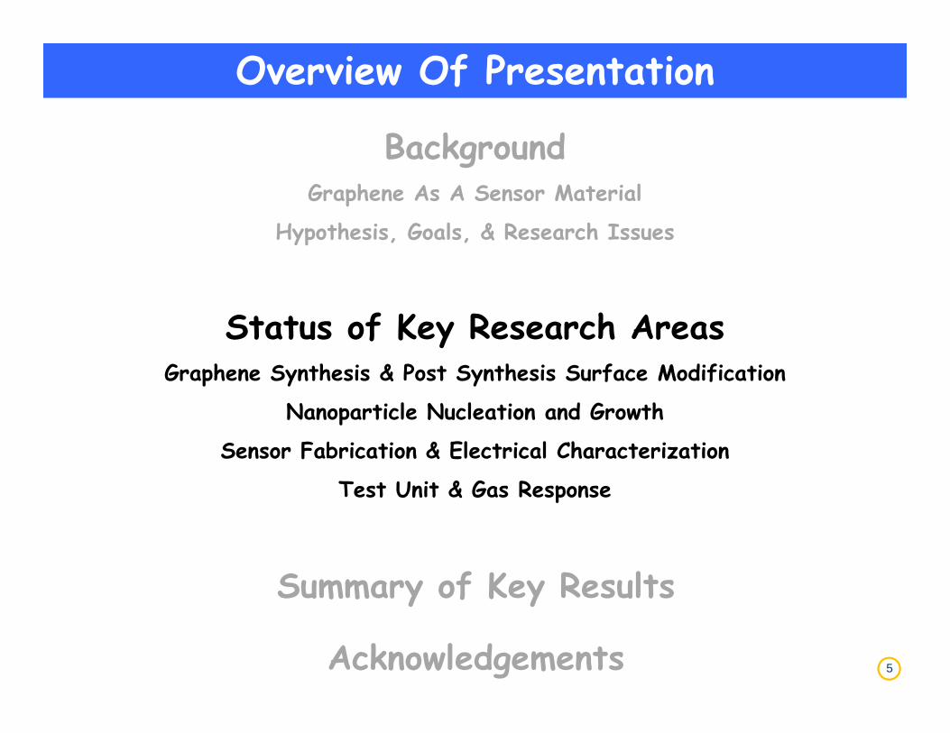
BackgroundGraphene As A Sensor Material
Hypothesis, Goals, & Research Issues
Overview Of Presentation
Status of Key Research AreasGraphene Synthesis & Post Synthesis Surface Modification
Nanoparticle Nucleation and Growth
Sensor Fabrication & Electrical Characterization
Test Unit & Gas Response
Summary of Key Results
Acknowledgements
3
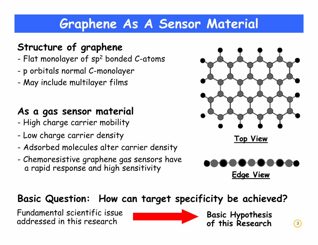
Graphene As A Sensor MaterialStructure of graphene
Basic Question: How can target specificity be achieved?
As a gas sensor material
- p orbitals normal C-monolayer
- Chemoresistive graphene gas sensors have a rapid response and high sensitivity
- Flat monolayer of sp2 bonded C-atoms
- High charge carrier mobility- Low charge carrier density- Adsorbed molecules alter carrier density
Fundamental scientific issue addressed in this research
- May include multilayer films
Top View
Edge View
Top View
Edge View
Basic Hypothesis of this Research
4
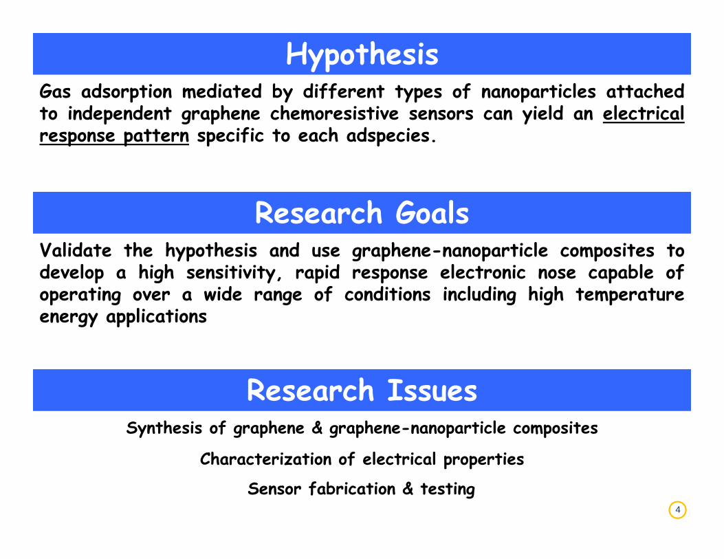
Gas adsorption mediated by different types of nanoparticles attachedto independent graphene chemoresistive sensors can yield an electricalresponse pattern specific to each adspecies.
Hypothesis
Research IssuesSynthesis of graphene & graphene-nanoparticle composites
Characterization of electrical properties
Sensor fabrication & testing
Validate the hypothesis and use graphene-nanoparticle composites todevelop a high sensitivity, rapid response electronic nose capable ofoperating over a wide range of conditions including high temperatureenergy applications
Research Goals
5
BackgroundGraphene As A Sensor Material
Hypothesis, Goals, & Research Issues
Overview Of Presentation
Status of Key Research AreasGraphene Synthesis & Post Synthesis Surface Modification
Nanoparticle Nucleation and Growth
Sensor Fabrication & Electrical Characterization
Test Unit & Gas Response
Summary of Key Results
Acknowledgements
6
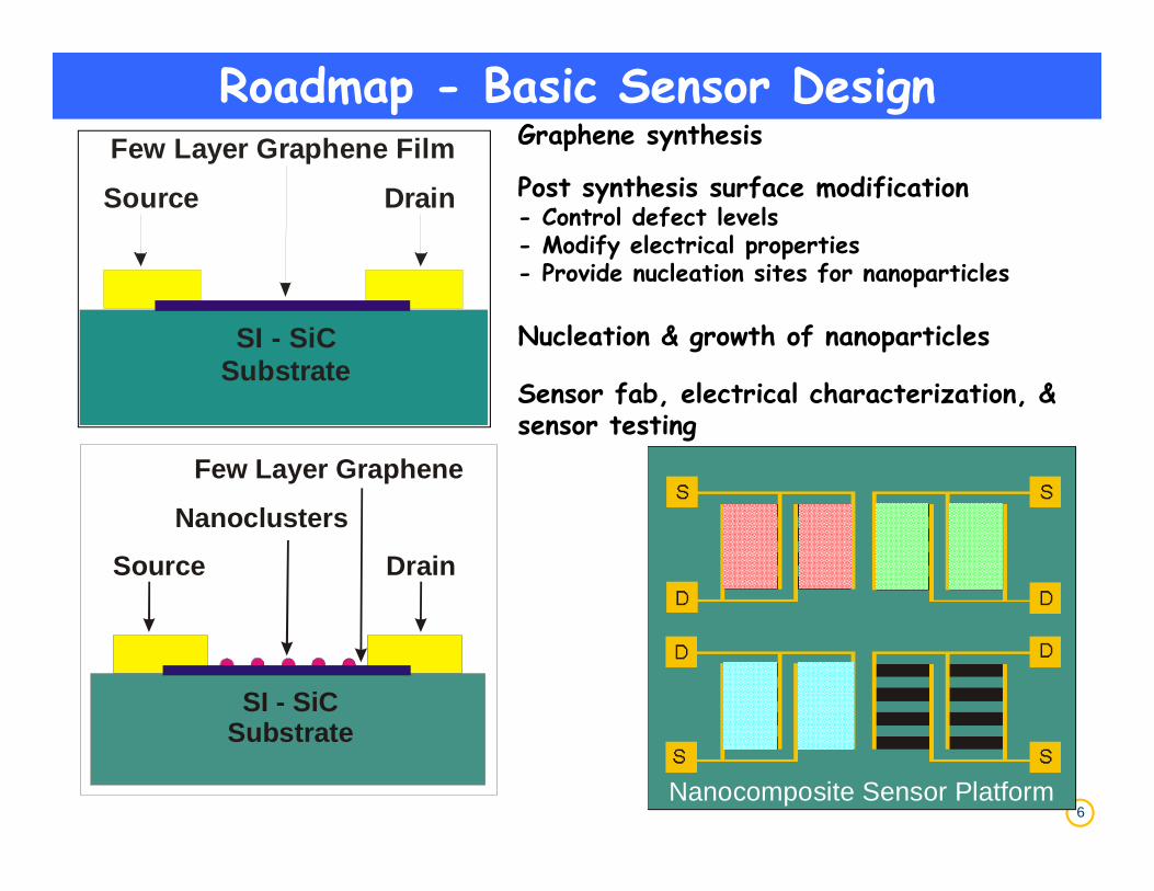
SI - SiC Substrate
Source Drain
Few Layer Graphene
Nanoclusters
Roadmap - Basic Sensor Design
SI - SiC Substrate
Source Drain
Few Layer Graphene Film Graphene synthesis
Post synthesis surface modification- Control defect levels- Modify electrical properties- Provide nucleation sites for nanoparticles
Nanocomposite Sensor Platform
Nucleation & growth of nanoparticles
Sensor fab, electrical characterization, & sensor testing
7
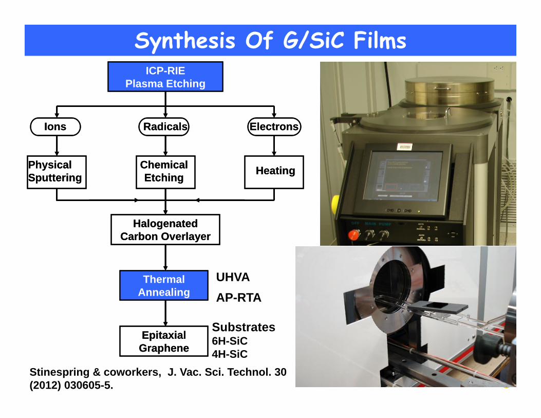
Synthesis Of G/SiC FilmsICP-RIE
Plasma Etching
Ions Radicals Electrons
PhysicalSputtering
Chemical Etching Heating
Halogenated Carbon Overlayer
ThermalAnnealing
EpitaxialGraphene
ICP-RIE Plasma Etching
Ions Radicals Electrons
PhysicalSputtering
Chemical Etching Heating
Halogenated Carbon Overlayer
ThermalAnnealing
EpitaxialGraphene
UHVAAP-RTA
Substrates6H-SiC4H-SiC
Stinespring & coworkers, J. Vac. Sci. Technol. 30 (2012) 030605-5.
8
680 685 690 695Binding Energy (eV)
Inte
nsity
(Arb
.Uni
ts) 687.6 eV
685.6 eV
F 1s - S35400 W ICP100 W RIE970oC
UHVA G/SiC Films
280 282 284 286 288 290
Binding Energy (eV)
Inte
nsity
(Arb
. Uni
ts)
C 1s - S40600 W ICP300 W RIE970oC282.5 eV
283.8 eV
285.6 eV288.1 eV
9
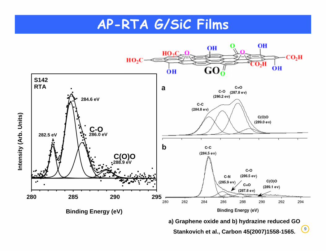
a) Graphene oxide and b) hydrazine reduced GO
Stankovich et al., Carbon 45(2007)1558-1565.
AP-RTA G/SiC Films
280 285 290 295
Inte
nsity
(Arb
. Uni
ts)
Binding Energy (eV)
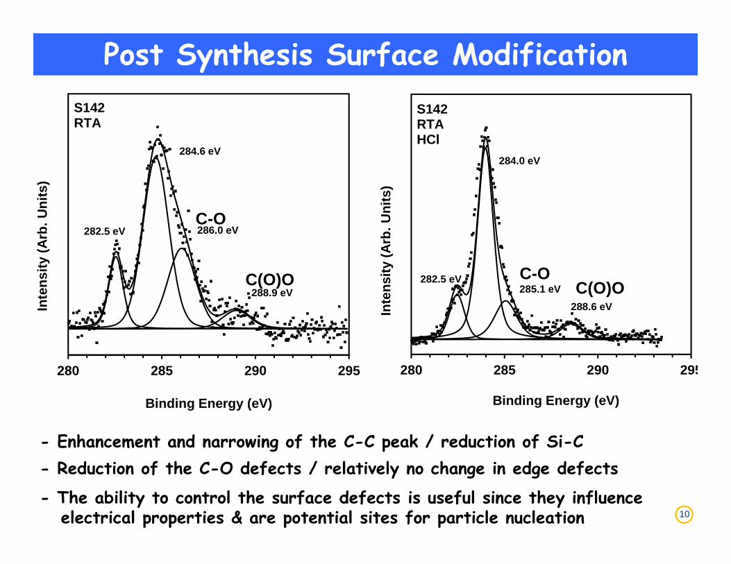
S142RTA
282.5 eV
284.6 eV
286.0 eV
288.9 eV
C-O
C(O)O
10
280 285 290 295
Inte
nsity
(Arb
. Uni
ts)
Binding Energy (eV)
S142RTA
282.5 eV
284.6 eV
286.0 eV
288.9 eV
280 285 290 295In
tens
ity (A
rb. U
nits
)Binding Energy (eV)
S142RTAHCl
282.5 eV
284.0 eV
285.1 eV288.6 eV
Post Synthesis Surface Modification
C-O
C(O)O C-OC(O)O
- Enhancement and narrowing of the C-C peak / reduction of Si-C- Reduction of the C-O defects / relatively no change in edge defects
- The ability to control the surface defects is useful since they influence electrical properties & are potential sites for particle nucleation

11
Nanoparticle Nucleation & Growth on GrapheneNanoparticles deposited on graphene from solution
Hypothesis is that particles will nucleate and grow on surface defects
Initial studies performed using Ag and Au nanoparticles Ag forms an oxide, Au does not
Both easily detected using SEM / XPS / AFM
Simple Reaction Mechanisms AgNO3 + NaBH4 > Ag + ½ H2 + ½ B2H6 + NaNO3
Simple Reaction Sequence Sample immersed in 10mM AgNO3/H2O
25mM NaBH4/H2O & incubated 12 hours Solomon et al., J. Chem. Ed. 84 (2007) 322-322.
Solomon et al., J. Chem. Ed. 84 (2007) 322-322.
12
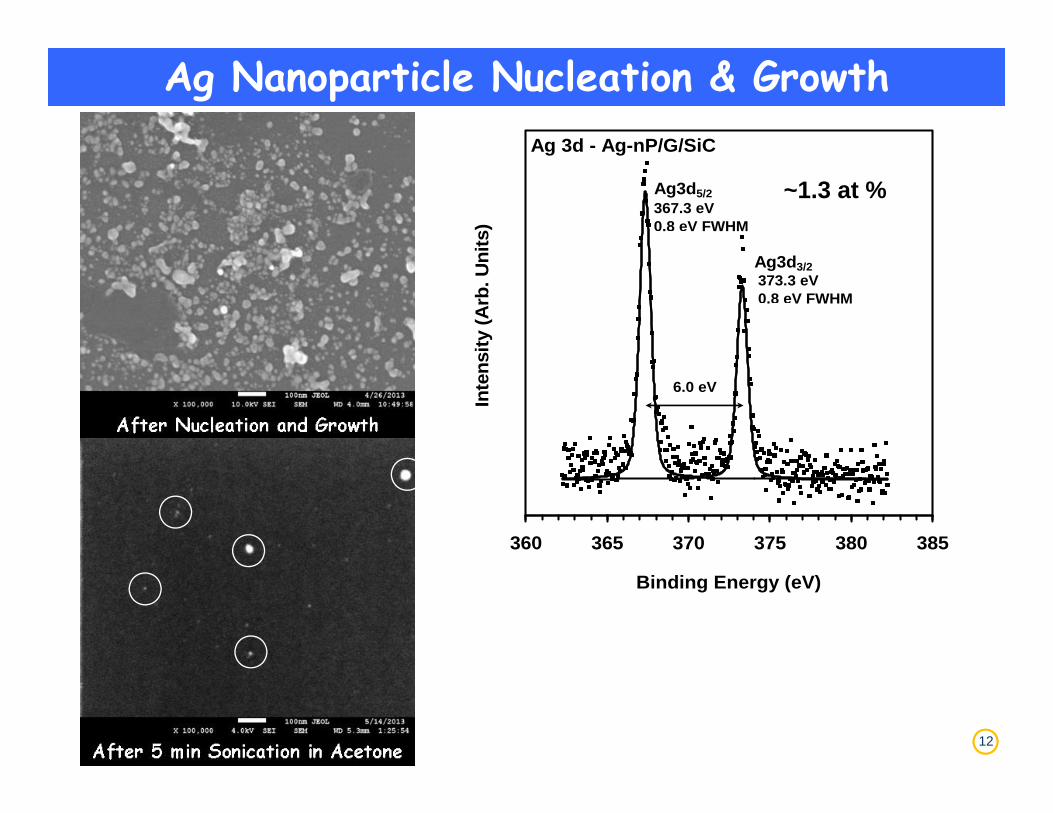
Ag Nanoparticle Nucleation & Growth
360 365 370 375 380 385
Binding Energy (eV)
Inte
nsity
(Arb
. Uni
ts)
Ag3d5/2
Ag3d3/2
367.3 eV0.8 eV FWHM
373.3 eV0.8 eV FWHM
6.0 eV
Ag 3d - Ag-nP/G/SiC
~1.3 at %

13
Au Nanoparticle Nucleation & Growth
2 µm x 2 µm AFM Image of Au np/G/SiC (S170) RMS ~ 6.0 nm 475 nm x 475 nm Image of Au np/G/SiC (S170) RMS ~ 5.8 nm 100 nm x 100 nm AFM Image of Au np/G/SiC (S170) RMS ~ 0.2 nm
0
2
4
6
8
10
0 100 200 300 400
[nm]
[nm]
Particle DimensionsDiameter: 25 nm – 150 nmHeight: 0.5 nm – 5 nm
- Attached particles are pyramidal- Suggests heterogeneous nucleation with
Volmer-Webber growth
- Ultrasonically removed particles are spheroidal- Associated with homogeneous nucleation &
deposition from solution
14
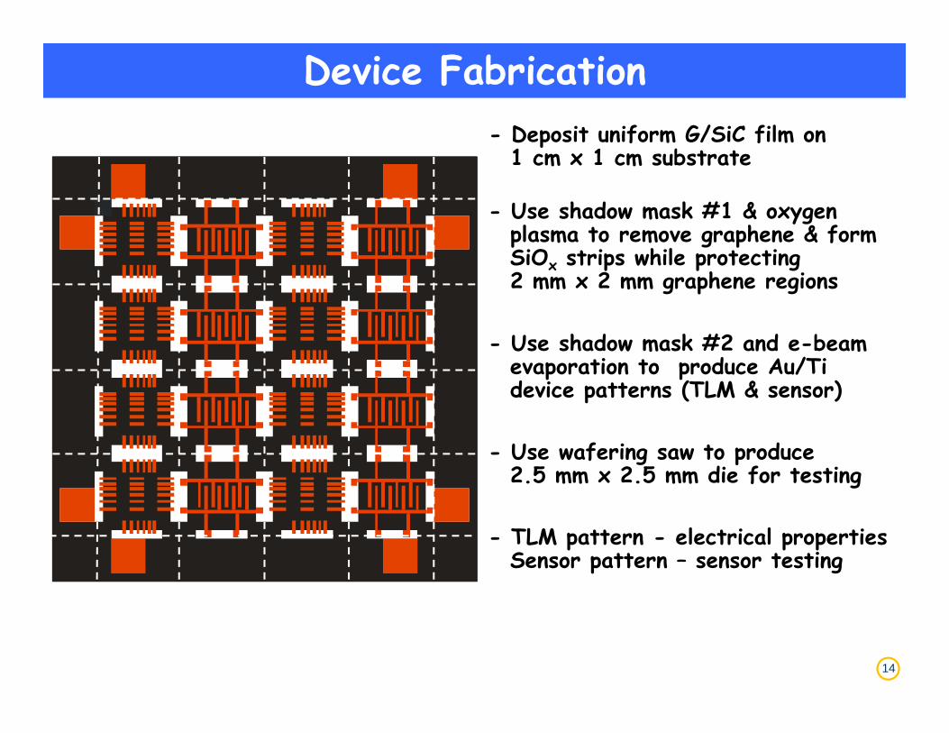
- Use shadow mask #1 & oxygen plasma to remove graphene & form SiOx strips while protecting 2 mm x 2 mm graphene regions
- Use shadow mask #2 and e-beam evaporation to produce Au/Ti device patterns (TLM & sensor)
- Use wafering saw to produce 2.5 mm x 2.5 mm die for testing
- Deposit uniform G/SiC film on1 cm x 1 cm substrate
Device Fabrication
- TLM pattern - electrical properties Sensor pattern – sensor testing
15
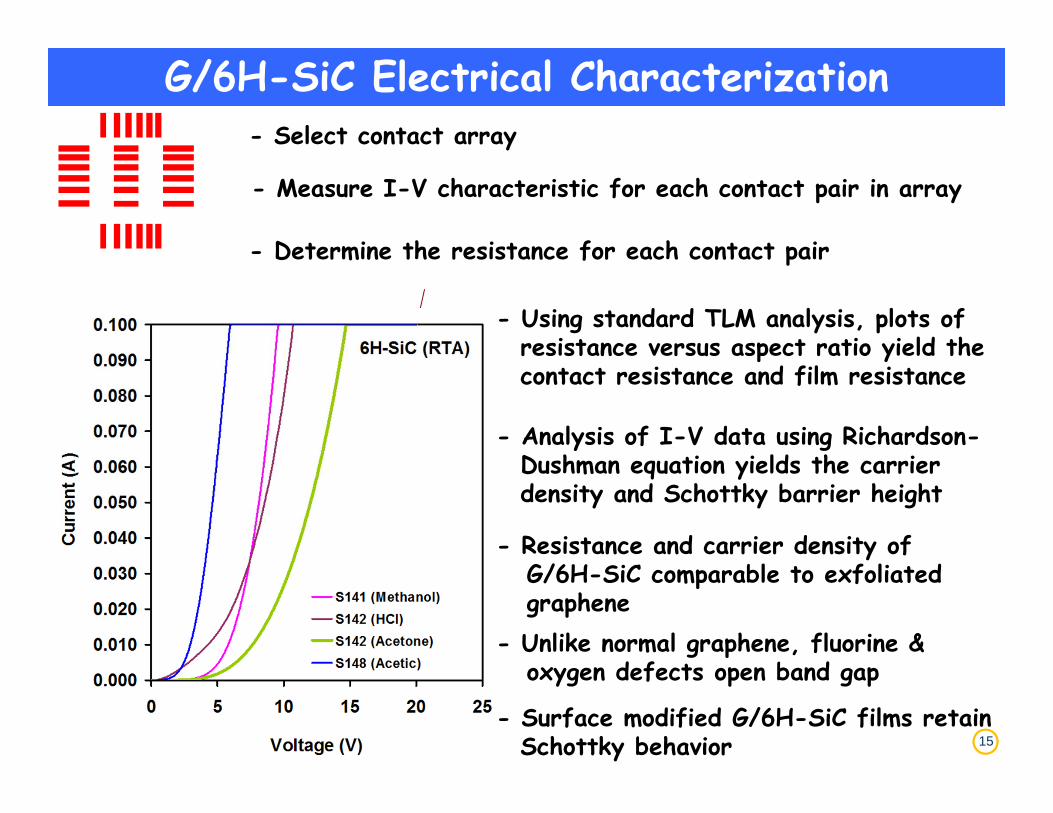
G/6H-SiC Electrical Characterization
0.000
0.002
0.004
0.006
0.008
0.010
0.012
0.014
0.016
0.018
0.020
0 1 2 3 4 5Voltage (V)
Cur
rent
(A)
S140
- Select contact array
- Analysis of I-V data using Richardson-Dushman equation yields the carrier density and Schottky barrier height
- Determine the resistance for each contact pair
Linear Fity = 0.3756x + 17.182
R2 = 0.9236
0
5
10
15
20
25
30
0 5 10 15Aspect Ratio (d/w)
Res
ista
nce
(Ohm
)
Slope = Sheet Resistance of Film (Ohm/sq)Intercept = 2*Contact Resistance (Ohm)
S140
Film Resistivity = 3.8 x 10⁻⁸ Ohm-cmContact Resistance = 8.3 Ohm
- Using standard TLM analysis, plots of resistance versus aspect ratio yield the contact resistance and film resistance
-12
-10
-8
-6
-4
-2
0
0.5 1.0 1.5 2.0
V1/4
Red
uced
Cur
rent
Carrier Density = 8.3 x 1011 cm-2
Schottky Barrier Height = 0.5 eV
- Resistance and carrier density of G/6H-SiC comparable to exfoliated graphene
- Unlike normal graphene, fluorine & oxygen defects open band gap
- Surface modified G/6H-SiC films retain Schottky behavior
- Measure I-V characteristic for each contact pair in array

16
G/4H-SiC Electrical Characterization- Both UHVA and RTA G/4H-SiC have low conductivity
- Surface modified G/4H-SiC exhibits Ohmic behavior
Summary- Electrical properties of native and
surface modified G/SiC quite diverse
- Raise interesting questions concerning the underlying physics
- Electrical properties well suited for next phase of sensor development
17
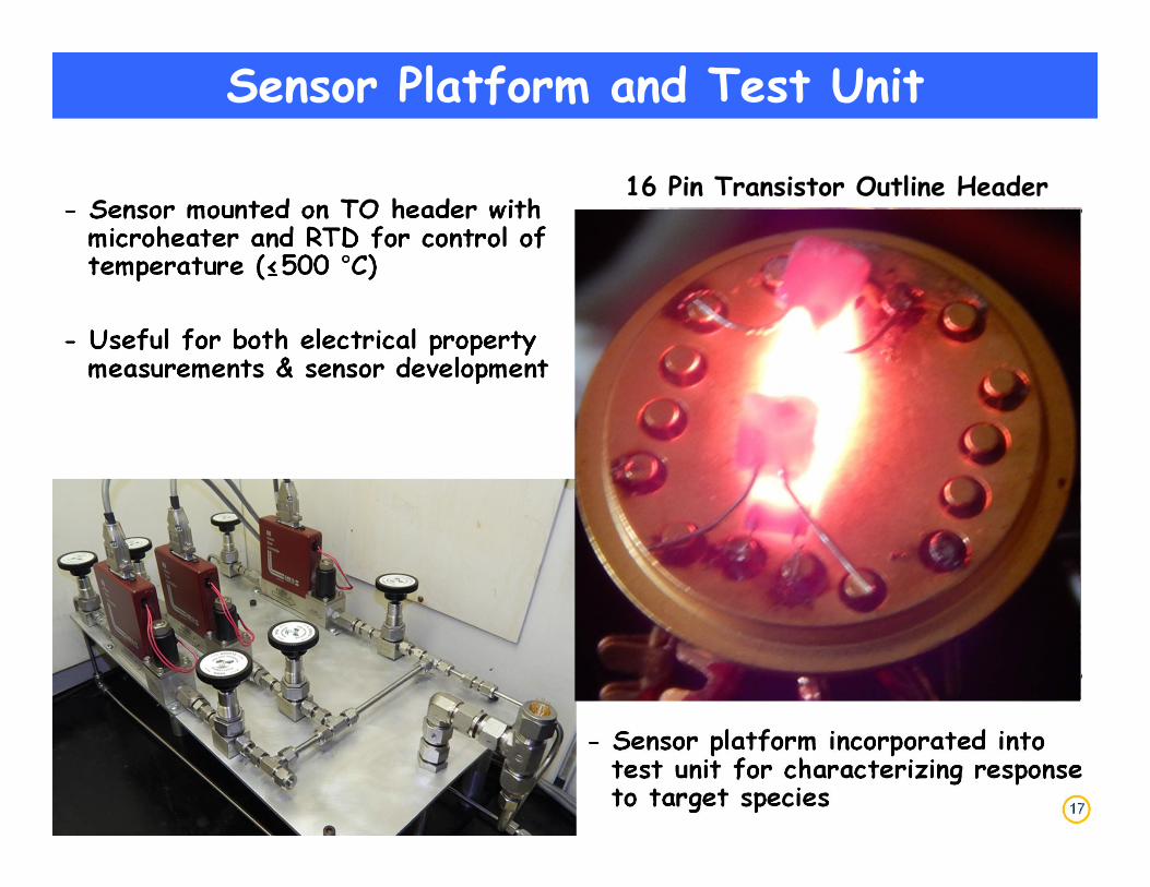
Sensor Platform and Test Unit
- Useful for both electrical property measurements & sensor development
- Sensor mounted on TO header with microheater and RTD for control of temperature (≤500 °C)
- Sensor platform incorporated into test unit for characterizing response to target species
16 Pin Transistor Outline Header

18
BackgroundGraphene As A Sensor Material
Hypothesis, Goals, & Research Issues
Task Schedule
Overview Of Presentation
Status of Key Research AreasGraphene Synthesis & Post Synthesis Surface Modification
Nanoparticle Nucleation and Growth
Sensor Fabrication & Electrical Characterization
Test Unit & Gas Response
Summary of Key Results
Acknowledgements
19
Synthesis & Post Synthesis Surface ModificationGraphene synthesis processes in hand- One, two, and three layer G/SiC reproducibly and routinely produced- UHVA and RTA defect structures characterized- Continue to optimize the process
Surface modification of continued interest - Surface modification alters defect distribution- Influences the electrical properties - May be useful in controlling the areal density of nucleation sites
20
Nanoparticle Nucleation and Growth
- Evidence for both homogeneously and heterogeneously nucleated particles- Brief ultrasonic treatment removes weakly attached particles- Pyramidal 0.5 – 5 nm high x 25 – 150 nn diameter particles remain- Suggest Volmer-Webber nucleation and growth mode- Studies in progress to establish role of defect sites & determine growth
kinetics
Studies of Pt, TiO2, and ZnO nucleation & growth next in line
Ag & Au nanoparticles deposited using solution chemistry

21
Sensor Fabrication & Electrical Characterization
- Native & surface modified G/SiC films exhibit diverse electrical properties - Raise highly interesting physics questions for further study
Sensor fabrication process in hand- Lithography free process developed for sensor & TLM structures- Continue to optimize process
Electrical characterization and testing in progress
Key Observation: The native & modified G/SiCwell suited for the sensor development and testing efforts now in progress
22
Acknowledgements
Undergrad Students- Jason Miles - Particle nucleation and growth- McKenzie Mills – Surface modification
PhD Students- Saurabh Chaudhari – Graphene synthesis & sensor fabrication- Andrew Graves – Sensor characterization
University Coal Research Program- DOE Award Number: DE-FEOO11300

23
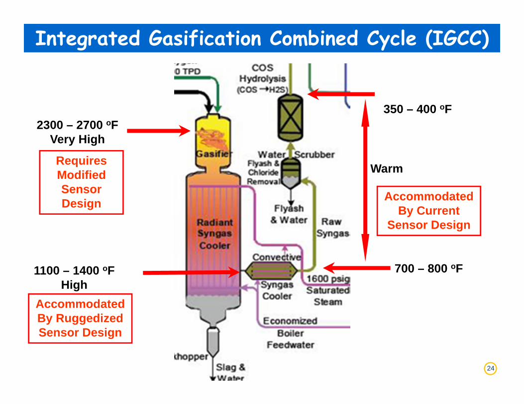
Looking Ahead – Applications EnvironmentIntegrated Gasification Combined Cycle
24
Integrated Gasification Combined Cycle (IGCC)
2300 – 2700 oFVery High
1100 – 1400 oFHigh
700 – 800 oF
350 – 400 oF
AccommodatedBy RuggedizedSensor Design
WarmRequiresModifiedSensorDesign Accommodated
By Current Sensor Design
25
Sensor Test Unit & Gas Response StudiesSensor test unit operational
Temperature dependent electrical characterization and gas response measurements in progress
26
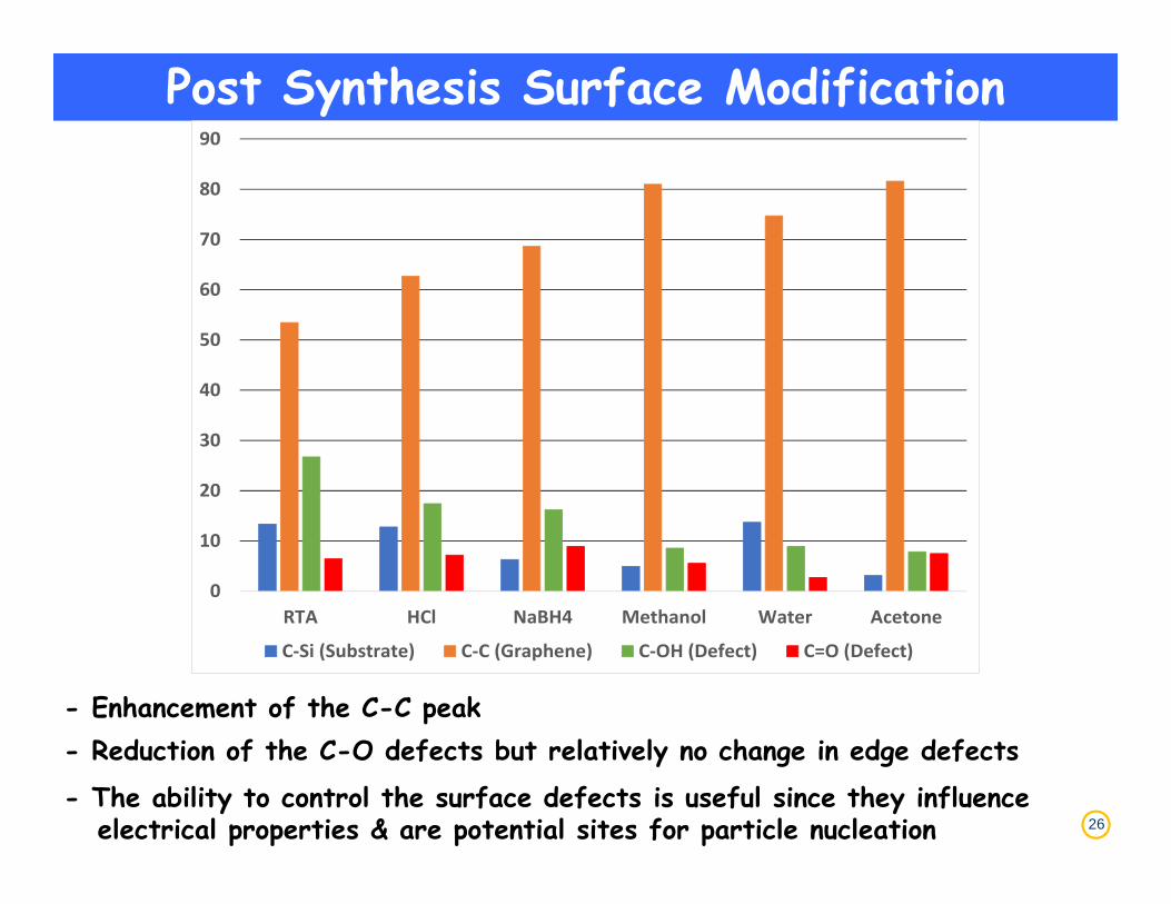
Post Synthesis Surface Modification
0
10
20
30
40
50
60
70
80
90
RTA HCl NaBH4 Methanol Water Acetone
C‐Si (Substrate) C‐C (Graphene) C‐OH (Defect) C=O (Defect)
- Enhancement of the C-C peak- Reduction of the C-O defects but relatively no change in edge defects
- The ability to control the surface defects is useful since they influence electrical properties & are potential sites for particle nucleation