guide to operation - martek power to operation i.electrical d ... dc converters utilize a unique...
TRANSCRIPT

GUIDE TO OPERATIONI. ELECTRICAL DESCRIPTION
The CB5/CB10D Series of DC-DC converters utilize a unique planar flyback power transformer while the CB30Sand CB75S converters use a planar forward converter topology to yield significantly greater power densities andlower output ripple. Advanced current mode control is utilized enabling a fast transient response time. Theswitching frequency of the CB Series are fixed at 500kHz(factory set; greater than 450kHz but less than 520 kHz) tominimize noise and allow for simplified EMI filtering (companion EMI modules are available). Sufficientcapacitance on the input and output, internal to the unit, allows for simple use and operation with no externalcomponents in most applications.
II. MECHANICAL DESCRIPTION
The CB5S/CB10D converters are encased in a 5 sided aluminum can, while the CB30S/CB75S converters areencased in a 5 sided steel can with an aluminum baseplate to facilitate heat transfer. The CB5S, CB10D, andCB30S height dimension of 0.38" allows for mounting in standard 1/2 inch width circuit card racks. The pins arenon-rigid and may be formed to suit specific mounting configurations. Care should be taken not to excessivelybend or over stress the pins to avoid breakage.
The high efficiency of the CB reduces heat dissipation and minimizes heat sinking requirements. Maximum dissipationat full load of CB5/CB10D will be between 1.1 and 1.67 watts per channel (between 5 and 7.5 watts for CB30S, andbetween 14 and 18.7 watts for the CB75S). Though this reduces heat sinking requirements, the baseplatetemperature must be maintained below +100°C.
Each CB unit has a label on it that will clearly identify pin functions and electrical ratings. Description of these functions can befound in the “Guide to Operation” and the “Application Notes” sections. Before electrically wiring the converterwe recommend carefully reviewing the application notes section entitled “General Application Notes” and “WireGage & Distance to Load”.
III. MILITARY SPECIFICATIONSEach CB unit is environmentally sealed and are designed to meet the following military environmental specifications:
The CB Series have been tested and found to meet the requirements of MIL-STD-461D for conducted emissions/interference on the input power leads (CE101 and CE102) when used with the CBF30 passive EMI filter. In addi-tion, the series have been designed to meet MIL-STD-461D for radiated emissions (RE101, RE102), conducted sus-ceptibility (CS101, CS114, CS115 and CS116) and radiated susceptibility (RS101, RS103).
IV. PRODUCT FEATURES
TTL (Remote on/off and Output status)
The TTL feature is used to command the CB series on and off and is referenced to the input return. When the TTLpin is left unconnected or, if a voltage between 2.4V and 5.0V is applied to the pin, the converter will remain on.
SpecificationMIL-STD-704D
MIL-STD-810E
MIL-STD-810E
MIL-STD-810EMIL-STD-810E
MIL-STD-810E
MIL-S-901C
ConditionInput Transient
Vibration
Humidity
Temp/Altitude
Acceleration
Temperature Shock
High Impact Shock
Method
514.4
507.3
520.1
513.4
503.3
Procedure
1
133
Test ConditionTransients up to 50 V for 0.1 second
Up to 30gs, each axis for 1 hour
95% humidity, non-condensing for 10 days
40 hours from -55°C to +71°C14gs each axis-55°C to +100°C(non-operating, one hour each cycle)5 foot hammer drop
www.martekpower.com
>> 341111 Knox Street Torrance CA 90502 USA Tel: +1 310 202 8820 [email protected]
When the TTL pin is pulled down below 0.8V the unit will turn off. For the CB5S, CB10D, and CB75S modules theTTL pin can be used as an output status indicator, with “high” indicating OK and “low” indicating out ofspecifications.
Over Temperature Protection (CB30S and CB75S only)
An integral electronic over temperature shut down circuit is provided to protect the CB series from accidental overheating. If the temperature (measured at the baseplate) of the converter exceeds 5% (105°C) above the ratedhigh operating temperature, the unit will automatically shut down. Once the temperature (measured at the base-plate) is reduced to 85% of the rated high operating temperature, power will be automatically restored.
Output Voltage Trim (CB30S and CB75S only)
An output voltage trim pin is provided for the adjustment of the output voltage and is referenced to the outputreturn. Using this feature the output voltage can be trimmed up to +10% of nominal and down to 90% of nomi-nal. To increase the output voltage, simply attach a resistor between the Trim pin and the Output Return of theunit. To decrease output voltage, simply attach a resistor between the Trim pin and +Output of the unit. ConsultApplication Notes for CB30S resistor values to achieve the desired output voltage for the CB30S.
Switching Frequency Synchronization (CB75S only)
The CB75S switching frequency is factory set to 500kHz. The converters can be synchronized to an externalsystem clock running at 480kHz to 550kHz by using the Sync Input pin. The Sync feature is a unidirectional inputonly, meaning that one converter cannot be used as a master to synchronize other slave modules - an externalsystem clock (referenced to the 28volt input return) will always be required for synchronization. See appliationnotes for more details.
Overload/Short Circuit Protection
The output of the CB Series is protected from an accidental overload or short circuit condition of any duration.When the output load exceeds the full load capability of the supply (105% to 150% of the maximum rated outputcurrent) the converter switches into a "Burp-Mode" (this is where the converter is sensing the overload and is continuouslyturning on and off in a controlled fashion). When the overload/short circuit is removed the converter automaticallyreturns to its normal mode of operation.
Over Voltage Protection
The CB series provides an internal overvoltage protection circuit. Should an overvoltage condition occur the converter will shutoff (output voltage will fall in accordance with Figure X). The CB5S/CB10D will auto recover when the overvoltage condition isremoved; for the CB30S and CB75S, the input must be recycled to restore output.
V. RELIABILITY
In order to achieve superior reliability, the CB series converters adhere to stringent component derating guidelinesbased on NAVMAT P4855-1. The Mean Time Between Failure (MTBF) per MIL-HBDK-217F Notice 2 calculated for theCB5S/CB10D operating at rated output power at three baseplates temperatures and various environments arecalculated in the following table. For the CB5SI, MTBF is calculated to be 457,192 hours GB, 71,000 hours NS, 50,840hours AIC, at 50°C baseplate. The MTBF per MIL-HBDK-217F Notice 2 calculated for the CB30SM under the operat-ing conditions of 50°C baseplate, maximum rated output is presented as a set of curves, based on Environment inthe main catalog. For the CB30SI, MTBF is calculated to be 5.04E5 GB, 7.57E4 NS, 5.12E4 AIC at +50oC.
www.martekpower.com
>> 351111 Knox Street Torrance CA 90502 USA Tel: +1 310 202 8820 [email protected]
CB30S MEAN TIME BETWEEN FAILURE (MTBF)
M Grade
GBGFGMNSNU
ARWAICAIFAUCAUFSFMFML CL
0ºC
5,216,680960,045526,940670,479294,991211,363487,795246,166314,272164,025
9,940,340371,820156,05711,969
25ºC
2,923,210527,222287,788389,076173,003118,718279,991143,593176,10894,529
5,495,230211,52888,5676,975
50ºC
1,525,930286,150154,885226,758102,51766,358161,76086,01999,05455,684
2,644,820119,75350,0654,026
100ºC
281,52778,88344,30873,07135,90920,83152,49331,62731,30519,910
361,51337,65016,1371,362
CB5S MEAN TIME BETWEEN FAILURE (MTBF)
Note: MTBF for CB10DM and CB10DI are 1/2 the values given above.
M Grade
GBGFGMNSNU
ARWAICAIFAUCAUFSFMFML CL
0ºC
4.33E+067.75E+054.15E+055.52E+052.40E+051.66E+053.96E+052.05E+052.49E+051.34E+058.33E+062.93E+051.23E+059.33E+03
10ºC
3.44E+066.02E+053.23E+054.41E+051.93E+051.31E+053.14E+051.64E+051.96E+051.07E+056.62E+062.33E+059.74E+047.50E+03
20ºC
2.72E+064.68E+052.51E+053.53E+051.55E+051.03E+052.50E+051.31E+051.54E+058.50E+045.21E+061.84E+057.71E+046.01E+03
30ºC
2.13E+063.63E+051.94E+052.82E+051.25E+058.09E+041.99E+051.06E+051.21E+056.81E+044.04E+061.46E+056.09E+044.80E+03
40ºC
1.66E+062.81E+051.50E+052.26E+051.01E+056.35E+041.59E+058.56E+049.54E+045.46E+043.09E+061.15E+054.80E+043.83E+03
50ºC
1.28E+062.18E+051.16E+051.81E+058.13E+044.99E+041.26E+056.95E+047.51E+044.39E+042.31E+069.11E+043.79E+043.05E+03
60ºC
9.72E+051.68E+058.93E+041.45+E056.57+E043.92E+041.01E+055.65E+045.92E+043.54E+041.69E+067.19E+042.99E+042.43E+03
70ºC
7.28E+051.30E+056.90E+041.16E+055.31E+043.08E+048.03E+044.60E+044.66E+042.86E+041.21E+065.67E+042.36E+041.93E+03
80ºC
5.37E+051.01E+055.34E+049.29E+044.29E+042.42E+046.40E+043.75E+043.68E+042.31E+048.44E+054.48E+041.87E+041.54E+03
I Grade
GBGFGMNSNU
ARWAICAIFAUCAUFSFMFML CL
0ºC
1,748,650318,726180,250214,01697,76771,005154,93276,85099,31450,851
3,228,880124,06852,6934,219
25ºC
941,481172,90196,436123,34669,4963,92188,54944,68855,53329,305
1,707,26069,53529,4002,400
50ºC
457,19292,21750,92271,10033,03521,67650,84026,69431,19217,280
743,06738,84416,4101,359
100ºC
67,79823,47713,70821,43411,0846,62215,7829,5899,6606,13081,13211,6985,161449
I Grade
GBGFGMNSNU
ARWAICAIFAUCAUFSFMFML CL
0ºC
1,970,000333,000181,000237,000105,00071,300167,00087,900
104,00056,500
3,610,000126,00053,3004,100
10ºC
1,540,000256000140,000190,00084,40055,900132,00070,00081,00044,800
2,840,00099,40041,9003,290
20ºC
1,200,000196,000107,000151,00067,70043,600105,00056,00063,30035,500
2,190,00078,10032,9002,620
30ºC
915,000149,00081,200120,00054,20033,90082,60044,90049,30028,300
1,640,00061,10025,7002,080
40ºC
687,000113,00061,60095,60043,40026,20065,10036,00038,30022,500
1,190,00047,70020,0001,640
50ºC
504,00085,90046,70075,70034,70020,30051,20029,00029,80017,900
833,00037,10015,6001,300
60ºC
362,00064,90035,30059,60027,70015,70040,20023,30023,10014,300
565,00028,80012,1001,020
70ºC
254,00049,00026,70046,80022,00012,10031,40018,70018,00011,400374,00022,4009,410801
80ºC
175,00036,90020,30036,50017,5009,40024,60015,00013,9009,080
243,00017,4007,330631
All specifications are typical @+25°C with nominal input voltage and under full output load conditions, unless otherwise noted. Specifications are subject to change without notice.
www.martekpower.com
>> 361111 Knox Street Torrance CA 90502 USA Tel: +1 310 202 8820 [email protected]
M Grade
GBGFGMNSNU
ARWAICAIFAUCAUFSFMFML CL
25ºC
1,320,660221,983130,647160,94573,63152,218112,36054,67370,70036,082
2,565,25092,10839,2223,406
50ºC
828,760139,07979,136109,62650,38033,10475,82238,71546,26825,046
1,526,33059,46425,1092,168
100ºC
211,84145,82625,33343,97721,17211,76630,10117,83517,35810,975
296,88221,6519,144795
CB75S MEAN TIME BETWEEN FAILURE (MTBF)
I Grade
GBGFGMNSNU
ARWAICAIFAUCAUFSFMFML CL
25ºC
413,28269,83041,78549,77323,09416,55334,69716,71521,84511,027
789,91429,08712,4571,109
50ºC
251,36643,91725,38633,96315,83610,54923,52811,88514,4107,704
444,74018,8528,013706
100ºC
54,07614,0578,011
13,2576,5933,7589,2425,4725,4333,40969,9956,8112,929260
All specifications are typical @+25°C with nominal input voltage and under full output load conditions, unless otherwise noted. Specifications are subject to change without notice.
www.martekpower.com
>> 371111 Knox Street Torrance CA 90502 USA Tel: +1 310 202 8820 [email protected]
GENERAL APPLICATION NOTES.......................................................................39
WIRE GAGE & DISTANCE TO LOAD.................................................................39
TTL & REMOTE ON/OFF................................................................................40
OUTPUT TRIM...............................................................................................40
RIPPLE & NOISE.......................................................................................45
SERIES OPERATION.....................................................................................46
REMOTE SENSE.....................................................................................46
SYNCHRONIZATION.....................................................................................46
ELECTRO MAGNETIC INTERFERENCE (EMI) FILTER .................................47
COMMON EQUATIONS....................................................................................48
BLOCK DIAGRAM...........................................................................................49
WARRANTY INFORMATION..............................................................................52
APPLICATION NOTES
All specifications are typical @+25°C with nominal input voltage and under full output load conditions, unless otherwise noted. Specifications are subject to change without notice.
www.martekpower.com
>> 381111 Knox Street Torrance CA 90502 USA Tel: +1 310 202 8820 [email protected]
General Application NotesThe CB series power converters were designed as military grade stand alone DC-DC converters which can also be used as components in complexpower systems. The CB5S/CB10D utilize a flybackconverter topology and the CB30S and CB75S powerconverters use a Forward converter topology. Advancedcurrent mode control is utilized enabling fast transientresponse time. The switching frequency is fixed at 500KHz to minimize noise and allow for simplified EMIfiltering. Sufficient capacitance on the input and output,internal to the unit, allows for simple use and operationwith no external components.
The CB5S/CB10D and the CB30S/CB75S units aresupplied in a five-sided and six-sided metal caserespectively to minimize radiated noise. TheCB5S/CB10D /CB30S height dimension of 0.38" allowsfor mounting in standard 1/2-inch width circuit cardracks. The CB series is available with pins out the base-plate for conduction cooling via a metal clad board. Thethermal operating range is -55 °C to +100 °C. All “M”
level units are fully screened similar to MIL-STD-883test procedures (see spec. sheets for details).The most basic use of the power converter is shown inFigure 1. An input fuse is always recommended toprotect both the source and the power supply in theevent of failures. Bus fuse type MDX or equivalentslow-blow is recommended with a current ratingapproximately 200% of the full load input current to theconverter. Having a slow-blow type fuse will allow for theconverter's inrush charge at turn-on. The CB series powerconverters comes with Current Limit, Short Circuit, OverVoltage protection, Trim (CB30S and CB75S only) andTTL as standard features.
Wire Gage &Distance to Load
If the resistance of the wire, printed circuit board runsor connectors used to connect a converter to systemcomponents is too high, excessive voltage drop willresult between the converter and system components,degrading overall system performance.
For example, if the DC/DC converter in Figure 2 is a50W unit (5 VDC @ 10 Amps) with output load regulationspecified at 0.2%; the connection as shown willdegrade load regulation by a factor of 10. In this example,the 4 feet of #14 AWG wire used to connect the converteroutput to the load, has a total line resistance of10mW(ignoring any contact resistance). For a 50W,5VDC output converter, the drop across the lead resistancewill be 100 mV (10 A X 0.010W ) or 2% of the output.
Thus, the converter was selected for 0.2% regulation,but the power system layout achieves only 2.2%.This can be corrected by decreasing the distancebetween the converter output and load. If that is notpossible, using larger diameter wire (see Table 1), orPCB runs that have a larger cross sectional area andshorter length will also reduce conductor resistance.The use of the converter's Trim capability is the idealmeans of hook-up.
Note: High IR drops between the converter and loadmay cause converter parameters such as output voltageaccuracy, trim range, etc. to appear to be out ofspecification. High IR drops on input lines may causestart up problems (voltage at the input pins below theinput range of the converter).
DCSOURCE LOAD
+Vin-Vin
TTL
+ OUT- OUT
TRIM
+-
Figure 1
Basic CB30S Converter Hook-up
DCSOURCE LOAD
+Vin-Vin
TTL
+ OUT- OUT
TRIM
+-
2 ft 14 AWG
2 ft 14 AWG
Figure 2
Converter Hook-Up Losses
#AWG
91011121314151617181920
ResistancemΩΩ / Foot
0.7920.9981.2611.5582.0012.5243.1814.0205.0546.3868.04610.13
#AWG
212223242526272829303132
ResistancemΩΩ / Foot
12.7716.2020.3025.6732.3741.0251.4465.3181.21103.7130.9162.0
Table 1. Wire Table Resistance
All specifications are typical @+25°C with nominal input voltage and under full output load conditions, unless otherwise noted. Specifications are subject to change without notice.
www.martekpower.com
>> 391111 Knox Street Torrance CA 90502 USA Tel: +1 310 202 8820 [email protected]
Obviously, any connections made to the powerdistribution bus may present a problem. Poorconnections (such as microcracking around solder joints)can cause serious problems such as arcing. Contactresistance must be minimized. Proper workmanshipstandards must be followed to insure reliable solderjoints for board mount converters.
Terminal strips, spade lugs and edge connectors must befree of any corrosion, dust or dirt. If parallel lines orconnections are available for routing converter outputcurrents, they should be utilized.
TTL & Remote On/OffThe TTL feature is especially useful in portable / mobile applications where battery powerconservation is critical.
The CB series employs a typical TTL open collector withinternal pull-up resistor. The voltage level at the TTL pin isreferenced with respect to the converter -Vin pin. Whenthe TTL circuit is pulled to less than 0.8 V ("logic 0") withrespect to the -Vin pin, via either an open collector (seeFigure 3), or optocoupler, or a mechanical switch, with a0.5mA capability, the converter shuts down. An optocou-pler (as shown) can also be used if the TTL signal needsto be referenced from the output side. If the TTL pin isleft floating or is pulled above 2.4V up to 5.0V ('logic 1')the unit will remain on. Many more devices can be usedto activate the TTL pin shutdown function, consult thefactory for your specific requirements.
Output Trim(CB30S, CB75S and CB150S only)
The output voltage can be increased or decreased (+10% Max, -10% Min.) by simply connecting a resistorbetween the trim pin and the Output Return pin or the+Output pin, respectively (see Figure 4).
The value of the resistor required to Trim Hi is shown inthe Table 2, 3 and 4. The external resistor is connectedbetween the Trim Pin and the Output Return Pin at thepower supply. (Use standard value 1% resistor closest tothe Table value).The value of the resistor required to TrimLo is shown in the Table 2 above. The external resistor isconnected between the Trim Pin and the +Output Pin atthe power supply. (Use standard value 1% resistorclosest to the Table value). A potentiometer can besubstituted for the resistor to achieve a more precise out-put voltage setting. Use the table resistor values todetermine the value of the potentiometer to use. CB75Sresistor values are shown in Table 3, Trim connectionsare same as CB30S except -Sense is used instead ofOutput Return (Trim Hi), and +Sense is used instead of+Output (Trim Lo).DC
SOURCE LOAD+Vin-Vin
TTL
+ OUT- OUT
TRIM
+-
Remote Turn On/Off
Figure 3
DCSOURCE LOAD
+Vin-Vin
TTL
+ OUT- OUT
TRIM
+-
TRIMHI
TRIMLO
Basic Trim Hook-up
Figure 4
All specifications are typical @+25°C with nominal input voltage and under full output load conditions, unless otherwise noted. Specifications are subject to change without notice.
www.martekpower.com
>> 401111 Knox Street Torrance CA 90502 USA Tel: +1 310 202 8820 [email protected]
Table 2 Output Trim Values (CB30S only)
2.202.102.001.901.80
8.918.2
OPEN9.53.8
3.633.473.303.142.97
1429.1
OPEN45
19.9
5.505.255.004.754.50
8.921.3
OPEN18.86.4
5.725.465.204.944.68
9.822.7
OPEN22.18.2
13.2012.6012.0011.4010.80
9.929.7
OPEN13255.9
16.5015.7515.0014.2513.50
10.731.3
OPEN18481
26.4025.2024.0022.8021.60
11.432.7
OPEN337153
30.8029.4028.0026.6025.20
12.835.5
OPEN429197
2Vout 3.3Vout 5Vout 5.2Vout 12Vout 15Vout 24Vout 28Vout
110% Vout
105% Vout
100% Vout
95% Vout
90% Vout
Volts kΩΩ Volts kΩΩ Volts kΩΩ Volts kΩΩ Volts kΩΩ Volts kΩΩ Volts kΩΩ Volts kΩΩ
Table 3 Output Trim Values (CB75S only)
2.202.102.001.901.80
2.617.32
OPEN2.94
0
3.633.473.303.142.97
07.87
OPEN16.23.24
5.505.255.004.754.50
09.31
OPEN44.215.4
5.725.465.204.944.68
09.53
OPEN47.516.9
13.2012.6012.0011.4010.80
019.6
OPEN12145.3
16.5015.7515.0014.2513.50
021.0
OPEN17869.8
26.425.224.022.821.6
022.6
OPEN348150
30.829.428.026.625.2
022.6
OPEN422187
2Vout 3.3Vout 5Vout 5.2Vout 12Vout 15Vout 24Vout 28Vout
110% Vout
105% Vout
100% Vout
95% Vout
90% Vout
Volts kΩΩ Volts kΩΩ Volts kΩΩ Volts kΩΩ Volts kΩΩ Volts kΩΩ Volts kΩΩ Volts kΩΩ
Table 4 Output Trim Values (CB150S only)
2.202.102.001.901.80
0.845.52
OPEN1.07
-
3.633.473.303.142.97
3.9011.6
OPEN19.76.89
5.505.255.004.754.50
5.4814.8
OPEN48.620.5
5.725.465.204.944.68
5.6515.1
OPEN53.622.9
13.2012.6012.0011.4010.80
7.2818.4
OPEN17781.4
16.5015.7515.0014.2513.50
7.7519.3
OPEN239111
26.425.224.022.821.6
8.1620.1
OPEN413193
30.829.428.026.625.2
18.941.7
OPEN435203
2Vout 3.3Vout 5Vout 5.2Vout 12Vout 15Vout 24Vout 28Vout
110% Vout
105% Vout
100% Vout
95% Vout
90% Vout
Volts kΩΩ Volts kΩΩ Volts kΩΩ Volts kΩΩ Volts kΩΩ Volts kΩΩ Volts kΩΩ Volts kΩΩ
All specifications are typical @+25°C with nominal input voltage and under full output load conditions, unless otherwise noted. Specifications are subject to change without notice.
www.martekpower.com
>> 411111 Knox Street Torrance CA 90502 USA Tel: +1 310 202 8820 [email protected]
The converter’s output voltage may be trimmed by up to ±10% of the nominal output voltage.
TRIM UP
Trim output voltage up by connecting an external resistor between Pins 6 and 5. Use the following equation,reference Table 5 for variables A and B.
Example:Trim 3%up for 5V Output units,where A = 1.25, B = 3.57, Δ% = 0.03
TTRIM DOWN
Trim output voltage down by connecting an external resistor between Pins 4 and 6. Use the followingequation, reference Table 6 for variables C and D.
Example:Trim 8% down for 15V Output units,where C = 10.3, D = 22.4, Δ% = 0.08
Radj-up =
Output Voltage Adjustment (CB30S)
A Δ %
- B (kΩ)
Radj-up = 1.25 0.03
- 3.57 kΩ = 38.1 kΩ
Radj-down = C Δ %
- D (kΩ)
Radj-down = 10.3 0.08
- 22.4 kΩ = 106 kΩ
Table 5.
2 0.930 0.4023.3 1.51 1.155 1.25 3.57
5.2 1.29 3.0112 1.97 1015 2.07 1024 2.14 1028 2.27 10
OutputVoltage(V) A B
Table 6.
2 0.57 1.9023.3 2.51 5.175 1.25 6.1
5.2 1.39 5.712 7.54 19.515 10.3 22.424 18.4 30.528 23.2 35.5
OutputVoltage(V) C D
All specifications are typical @+25°C with nominal input voltage and under full output load conditions, unless otherwise noted. Specifications are subject to change without notice.
www.martekpower.com
>> 421111 Knox Street Torrance CA 90502 USA Tel: +1 310 202 8820 [email protected]

The converter’s output voltage may be trimmed by up to ±10% of the nominal output voltage.
TRIM UP
Trim output voltage up by connecting an external resistor between Pins 7 and 8. Use the following equation,reference Table 7 for variables A and B.
Example:Trim 5% up for 5V Output units,where A = 0.931, B = 9.09, Δ% = 0.05
TTRIM DOWN
Trim output voltage down by connecting an external resistor between Pins 7 and 6. Use the followingequation, reference Table 8 for variables C and D.
Example:Trim 10% down for 15V Output units,where C = 10.3, D = 32.4, Δ% = 0.1
Radj-up =
Output Voltage Adjustment (CB75S)
A Δ %
- B (kΩ)
Radj-up = 0.931 0.05
- 9.09 kΩ = 9.53 kΩ
Radj-down = C Δ %
- D (kΩ)
Radj-down = 10.3 0.1
- 32.4 kΩ = 70.6 kΩ
Table 7.
2 0.467 23.3 0.773 7.55 0.931 9.09
5.2 0.942 9.0912 1.97 19.115 2.08 2024 2.24 22.128 2.28 22.6
OutputVoltage(V) A B
Table 8.
2 0.283 2.753.3 1.28 9.555 2.81 12.8
5.2 2.98 13.012 7.34 28.415 10.3 32.424 19.3 43.628 23.2 48.1
OutputVoltage(V) C D
All specifications are typical @+25°C with nominal input voltage and under full output load conditions, unless otherwise noted. Specifications are subject to change without notice.
www.martekpower.com
>> 431111 Knox Street Torrance CA 90502 USA Tel: +1 310 202 8820 [email protected]
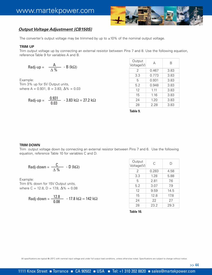
The converter’s output voltage may be trimmed by up to ±10% of the nominal output voltage.
TRIM UP
Trim output voltage up by connecting an external resistor between Pins 7 and 8. Use the following equation,reference Table 9 for variables A and B.
Example:Trim 3% up for 5V Output units,where A = 0.931, B = 3.83, Δ% = 0.03
TTRIM DOWN
Trim output voltage down by connecting an external resistor between Pins 7 and 6. Use the followingequation, reference Table 10 for variables C and D.
Example:Trim 8% down for 15V Output units,where C = 12.8, D = 17.8, Δ% = 0.08
Radj-up =
Output Voltage Adjustment (CB150S)
A Δ %
- B (kΩ)
Radj-up = 0.931 0.03
- 3.83 kΩ = 27.2 kΩ
Radj-down = C Δ %
- D (kΩ)
Radj-down = 12.8 0.08
- 17.8 kΩ = 142 kΩ
Table 9.
2 0.467 3.833.3 0.773 3.835 0.931 3.83
5.2 0.948 3.8312 1.11 3.8315 1.16 3.8324 1.20 3.8328 2.28 3.83
OutputVoltage(V) A B
Table 10.
2 0.283 4.583.3 1.28 5.885 2.81 7.6
5.2 3.07 7.912 9.59 14.515 12.8 17.824 22 2728 23.2 29.3
OutputVoltage(V) C D
All specifications are typical @+25°C with nominal input voltage and under full output load conditions, unless otherwise noted. Specifications are subject to change without notice.
www.martekpower.com
>> 441111 Knox Street Torrance CA 90502 USA Tel: +1 310 202 8820 [email protected]
Ripple & Noise
Output ripple and noise (sometimes referred toas PARD or “Periodic and Random Deviations”) can bedefined as unwanted variations in the output voltage ofa power supply. In switching power supplies thisoutput noise is seen as a series of pulses with a highfrequency content and is therefore measured as a peakvalue (i.e., specified as “peak-to-peak”).
Martek Power Abbott, Inc. CB series of power suppliesare specified and tested in our factory with a 10 MHzbandwidth oscilloscope/probe. Measurements taken by ascope set at higher frequencies (i.e. 300 MHz) may producesignificantly different results due to noise coupling on tothe probe from sources other than the power supply.
Noise that is common to all output leads of a powerconverter with respect to the chassis is referred to ascommon mode noise. Noise that is apparent on oneoutput lead with respect to the other output lead isreferred to as differential mode noise. Common modenoise is produced in switching action. Martek PowerAbbott, Inc. typically minimizes the level of output com-mon mode noise by incorporating line to chassis groundcapacitors (on input and output leads) into the powerconverters. In most cases this is sufficient to minimizethe level of common mode noise. However, if furtherattenuation is required, additional line to chassis groundcapacitance may be added by the customer at the systemlevel. Martek Power Abbott, Inc. noise specifications(output ripple specifications) all reference the level ofdifferential mode noise at a given bandwidth, not thelevel of common mode noise. The measurement of differentialmode noise is detailed in the following paragraphs.
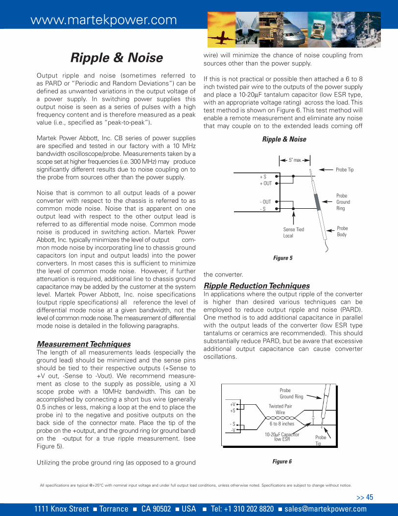
Measurement TechniquesThe length of all measurements leads (especially theground lead) should be minimized and the sense pinsshould be tied to their respective outputs (+Sense to+V out, -Sense to -Vout). We recommend measure-ment as close to the supply as possible, using a XIscope probe with a 10MHz bandwidth. This can beaccomplished by connecting a short bus wire (generally0.5 inches or less, making a loop at the end to place theprobe in) to the negative and positive outputs on theback side of the connector mate. Place the tip of theprobe on the +output, and the ground ring (or ground band)on the -output for a true ripple measurement. (seeFigure 5).
Utilizing the probe ground ring (as opposed to a ground
wire) will minimize the chance of noise coupling fromsources other than the power supply.
If this is not practical or possible then attached a 6 to 8inch twisted pair wire to the outputs of the power supplyand place a 10-20μF tantalum capacitor (low ESR type,with an appropriate voltage rating) across the load. Thistest method is shown on Figure 6. This test method willenable a remote measurement and eliminate any noisethat may couple on to the extended leads coming off
the converter.
Ripple Reduction TechniquesIn applications where the output ripple of the converteris higher than desired various techniques can beemployed to reduce output ripple and noise (PARD).One method is to add additional capacitance in parallelwith the output leads of the converter (low ESR typetantalums or ceramics are recommended). This shouldsubstantially reduce PARD, but be aware that excessiveadditional output capacitance can cause converteroscillations.
Figure 5
Ripple & Noise
Sense TiedLocal
Probe Tip+ S+ OUT
- OUT- S
ProbeGroundRing
ProbeBody
.5” max.
Figure 6
+V+S
- S-V
Twisted Pair Wire
6 to 8 inches
10-20μF Capacitorlow ESR
ProbeGround Ring
ProbeTip
All specifications are typical @+25°C with nominal input voltage and under full output load conditions, unless otherwise noted. Specifications are subject to change without notice.
www.martekpower.com
>> 451111 Knox Street Torrance CA 90502 USA Tel: +1 310 202 8820 [email protected]
Remote SenseRemote sense pins, +S (or + SENSE) and -S (or-SENSE) have been provided on selected CB Seriesconverters for applications where precise loadregulation is required at a distance from where theconverter is physically located. (Not all converters havethis feature. Check specific data sheets for details.) Ifremote sensing is NOT required, these pins MUST be
tied to their respective output pins (+S to +OUT and -Sto -OUT). If one or more of these sense pins are notconnected to their respective output pins, the output(s)of the unit will not regulate to within specification andmay cause a high output voltage condition. .
• DO NOT connect sense pins to any pin otherthan their respective output pins or permanent damagewill occur.
• DO NOT connect sense pins to any load otherthan the same load the output pins are connected to orpermanent damage may occur.
The internal remote sense circuit is designed tocompensate for a maximum of 0.5V difference (0.25V ineach output lead) in voltage between the load and thepower converter. Longer output leads or traces arerequired to be of sufficient gauge or width to maintainthe voltage drop across them of 0.5V maximum at ratedload current.
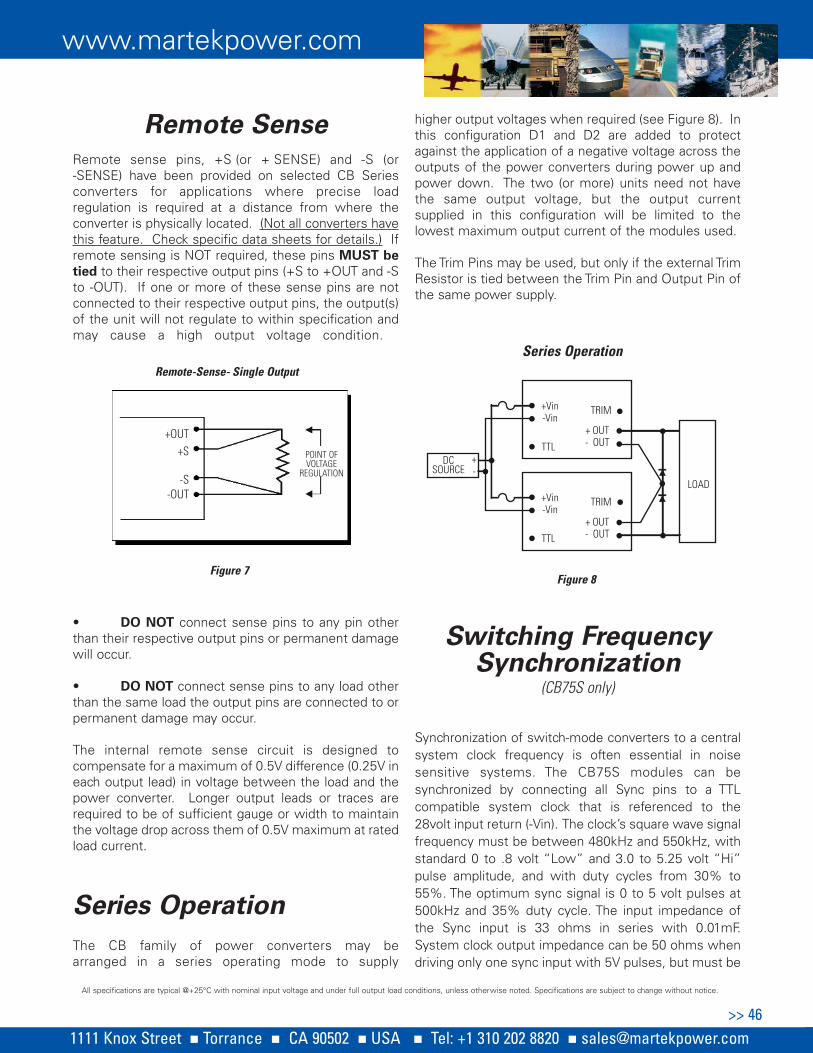
Series Operation
The CB family of power converters may be arranged in a series operating mode to supply
higher output voltages when required (see Figure 8). Inthis configuration D1 and D2 are added to protectagainst the application of a negative voltage across theoutputs of the power converters during power up andpower down. The two (or more) units need not havethe same output voltage, but the output currentsupplied in this configuration will be limited to thelowest maximum output current of the modules used.
The Trim Pins may be used, but only if the external TrimResistor is tied between the Trim Pin and Output Pin ofthe same power supply.
Switching FrequencySynchronization
(CB75S only)
Synchronization of switch-mode converters to a centralsystem clock frequency is often essential in noisesensitive systems. The CB75S modules can besynchronized by connecting all Sync pins to a TTLcompatible system clock that is referenced to the28volt input return (-Vin). The clock’s square wave signalfrequency must be between 480kHz and 550kHz, withstandard 0 to .8 volt “Low” and 3.0 to 5.25 volt “Hi”pulse amplitude, and with duty cycles from 30% to55%. The optimum sync signal is 0 to 5 volt pulses at500kHz and 35% duty cycle. The input impedance ofthe Sync input is 33 ohms in series with 0.01mF.System clock output impedance can be 50 ohms whendriving only one sync input with 5V pulses, but must be
LOAD
+Vin-Vin
TTL
+ OUT- OUT
TRIM
DCSOURCE
+-
+Vin-Vin
TTL
+ OUT- OUT
TRIM
Series Operation
Figure 8
All specifications are typical @+25°C with nominal input voltage and under full output load conditions, unless otherwise noted. Specifications are subject to change without notice.
+OUT+S
-S-OUT
POINT OFVOLTAGE
REGULATION
Figure 7
Remote-Sense- Single Output
www.martekpower.com
>> 461111 Knox Street Torrance CA 90502 USA Tel: +1 310 202 8820 [email protected]

standard TTL or CMOS totem pole output when drivingmultiple converters, especially with 3V pulses. Caremust be taken in how the Sync pin is connected to thesystem clock -- in some cases shielding of the Syncsignal will help eliminate noise problems. Do not addany capacitance from the Sync signal to -Vin.
ElectromagneticInterference (EMI) Filter
For applications where Electromagnetic Interference is a concern, the CBF30, a passive inputfilter may be installed at the input of the CB5S/CB10D/CB30S converters (see Figure 9).
With the EMI filter MIL-STD-461D, CE101 and CE102are within compliance on the input leads. Test reportscharacterizing filters for conducted and radiatedemission and susceptibility are available. Filters guaranteeconducted emissions (on the input leads) only. All testreports are certified by an independent testing lab.TheCB75S’s companion EMI filter, the CBF75 will undergoformal emissions and susceptibility testing soon.Engineering samples are currently available. During MIL-STD-461D testing, CTEST is required across the outputs oftwo LISNs, as shown in Figure 9. CTEST is 47μF@100Valuminum electrolytic such as United Chemi-Con styleKME or equivalent. CTEST is not required for normaloperation, or for MIL-STD-461C testing.
All specifications are typical @+25°C with nominal input voltage and under full output load conditions, unless otherwise noted. Specifications are subject to change without notice.
MIL-STD-461D Test Set-up
Figure 10
DCSOURCE
LISN
LISNCB75 LOAD
+
-
+
-
EMIFILTER
+
-
+
- CTEST
DCSOURCE
LOAD
+Vin-Vin
TTL+ OUT- OUT
TRIM+-
EMI FILTER
+Vin-Vin
+OUT- OUT
Figure 9
EMI Filter Connection
www.martekpower.com
>> 471111 Knox Street Torrance CA 90502 USA Tel: +1 310 202 8820 [email protected]
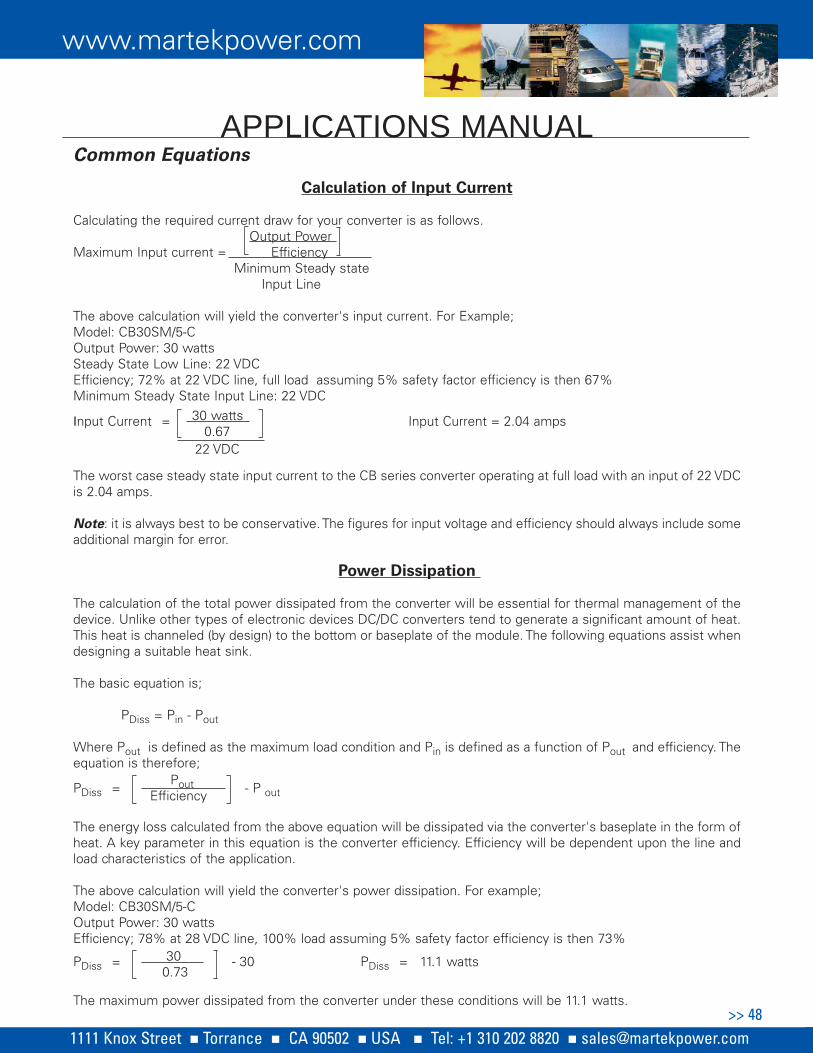
Common Equations
Calculation of Input Current
Calculating the required current draw for your converter is as follows. Output Power
Maximum Input current = Efficiency Minimum Steady state
Input Line
The above calculation will yield the converter's input current. For Example;Model: CB30SM/5-COutput Power: 30 wattsSteady State Low Line: 22 VDCEfficiency; 72% at 22 VDC line, full load assuming 5% safety factor efficiency is then 67%Minimum Steady State Input Line: 22 VDC
The worst case steady state input current to the CB series converter operating at full load with an input of 22 VDCis 2.04 amps.
Note: it is always best to be conservative. The figures for input voltage and efficiency should always include someadditional margin for error.
Power Dissipation
The calculation of the total power dissipated from the converter will be essential for thermal management of thedevice. Unlike other types of electronic devices DC/DC converters tend to generate a significant amount of heat.This heat is channeled (by design) to the bottom or baseplate of the module. The following equations assist whendesigning a suitable heat sink.
The basic equation is;
PDiss = Pin - Pout
Where Pout is defined as the maximum load condition and Pin is defined as a function of Pout and efficiency. Theequation is therefore;
The energy loss calculated from the above equation will be dissipated via the converter's baseplate in the form ofheat. A key parameter in this equation is the converter efficiency. Efficiency will be dependent upon the line andload characteristics of the application.
The above calculation will yield the converter's power dissipation. For example; Model: CB30SM/5-COutput Power: 30 wattsEfficiency; 78% at 28 VDC line, 100% load assuming 5% safety factor efficiency is then 73%
The maximum power dissipated from the converter under these conditions will be 11.1 watts.
PDiss = - P outPout
Efficiency
PDiss = - 30 PDiss = 11.1 watts30 0.73
Input Current = Input Current = 2.04 amps
22 VDC
30 watts0.67
APPLICATIONS MANUAL
www.martekpower.com
>> 481111 Knox Street Torrance CA 90502 USA Tel: +1 310 202 8820 [email protected]
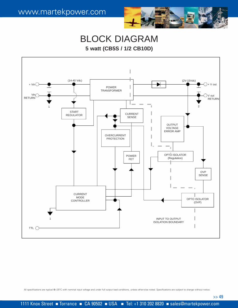
BLOCK DIAGRAM5 watt (CB5S / 1/2 CB10D)
(14-40 Vdc)+ Vin
TTL
1
(2V-15Vdc)+ V out
V outRETURN
2
POWERTRANSFORMER
OPTO ISOLATOR(Regulation)
STARTREGULATOR
1
CURRENTSENSE
OVERCURRENTPROTECTION
POWERFET
OVPSENSE
OPTO ISOLATOR(OVP)
OUTPUTVOLTAGE
ERROR AMP
CURRENTMODE
CONTROLLER
INPUT TO OUTPUTISOLATION BOUNDARY
VinRETURN
All specifications are typical @+25°C with nominal input voltage and under full output load conditions, unless otherwise noted. Specifications are subject to change without notice.
www.martekpower.com
>> 491111 Knox Street Torrance CA 90502 USA Tel: +1 310 202 8820 [email protected]
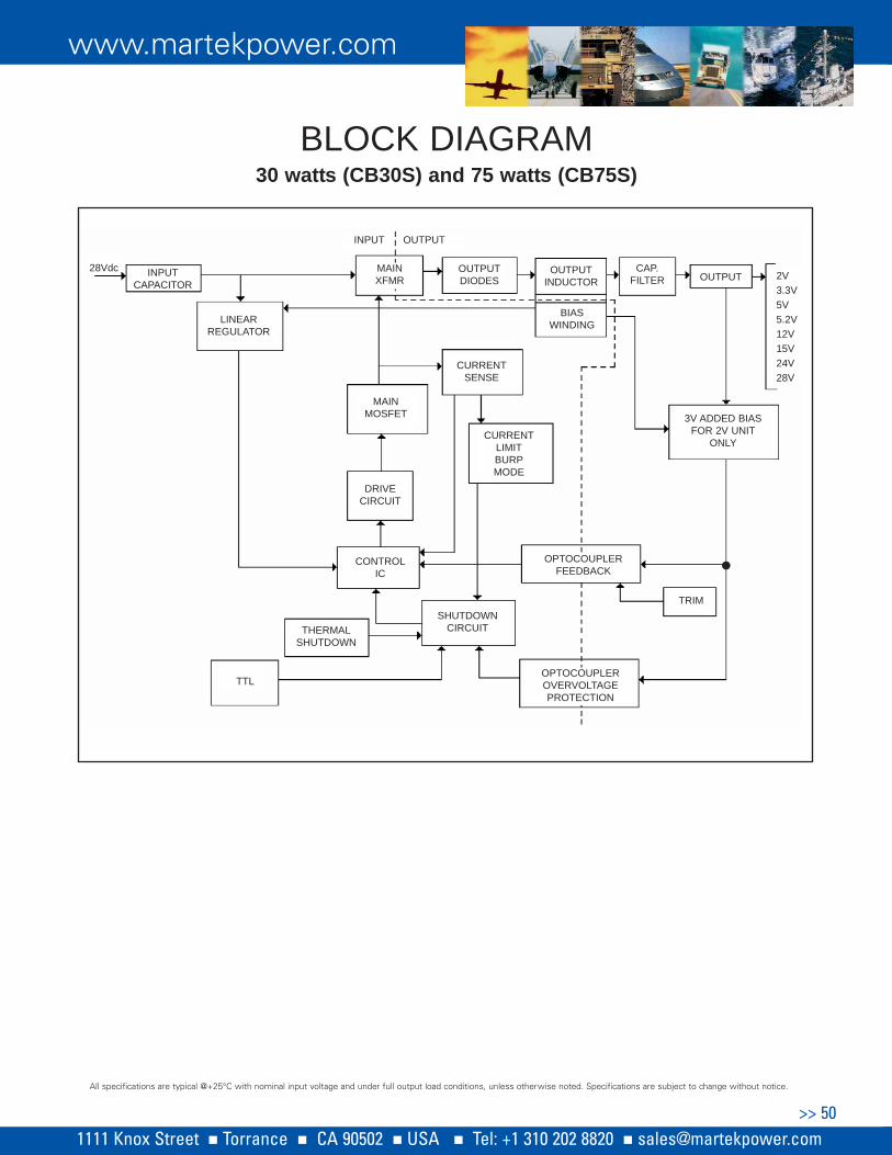
BLOCK DIAGRAM30 watts (CB30S) and 75 watts (CB75S)
3V ADDED BIASFOR 2V UNIT
ONLY
LINEARREGULATOR
INPUTCAPACITOR
MAINXFMR
OUTPUTDIODES
OUTPUTINDUCTOR
BIASWINDING
CAP.FILTER OUTPUT
MAINMOSFET
DRIVECIRCUIT
CURRENTSENSE
CURRENTLIMITBURPMODE
CONTROLIC
THERMALSHUTDOWN
TTL
OPTOCOUPLERFEEDBACK
SHUTDOWNCIRCUIT
OPTOCOUPLEROVERVOLTAGEPROTECTION
TRIM
2V3.3V5V5.2V12V15V24V28V
INPUT OUTPUT
28Vdc
All specifications are typical @+25°C with nominal input voltage and under full output load conditions, unless otherwise noted. Specifications are subject to change without notice.
www.martekpower.com
>> 501111 Knox Street Torrance CA 90502 USA Tel: +1 310 202 8820 [email protected]
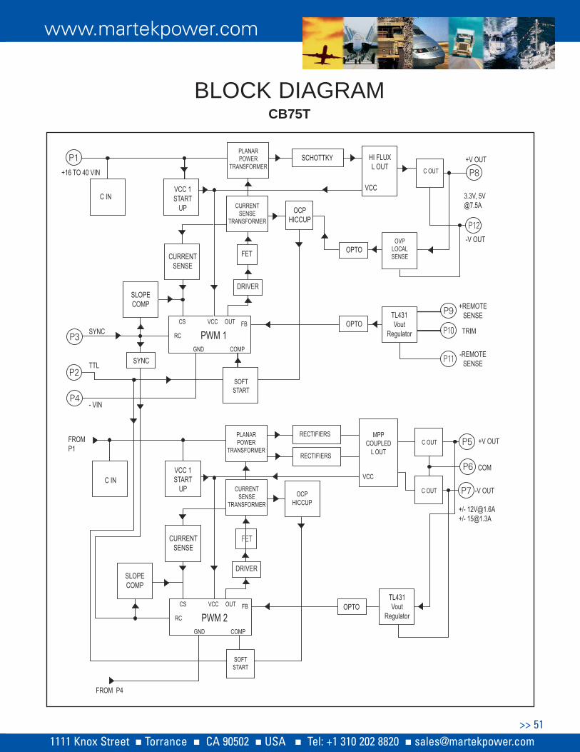
BLOCK DIAGRAMCB75T
www.martekpower.com
>> 511111 Knox Street Torrance CA 90502 USA Tel: +1 310 202 8820 [email protected]