h-bridge inverter loading analysis for an energy management … · from a single phase pulse-width...
TRANSCRIPT

Calhoun: The NPS Institutional Archive
Theses and Dissertations Thesis Collection
2013-06
H-bridge inverter loading analysis for an Energy
Management System
Metzcus, Andrew James
Monterey, California: Naval Postgraduate School
http://hdl.handle.net/10945/34706

NAVAL
POSTGRADUATE
SCHOOL
MONTEREY, CALIFORNIA
THESIS
Approved for public release; distribution is unlimited
H-BRIDGE INVERTER LOADING ANALYSIS FOR AN ENERGY MANAGEMENT SYSTEM
by
Andrew James Metzcus
June 2013
Thesis Advisor: Giovanna Oriti Co-Advisor: Alexander L. Julian

THIS PAGE INTENTIONALLY LEFT BLANK

i
REPORT DOCUMENTATION PAGE Form Approved OMB No. 0704-0188Public reporting burden for this collection of information is estimated to average 1 hour per response, including the time for reviewing instruction, searching existing data sources, gathering and maintaining the data needed, and completing and reviewing the collection of information. Send comments regarding this burden estimate or any other aspect of this collection of information, including suggestions for reducing this burden, to Washington headquarters Services, Directorate for Information Operations and Reports, 1215 Jefferson Davis Highway, Suite 1204, Arlington, VA 22202-4302, and to the Office of Management and Budget, Paperwork Reduction Project (0704-0188) Washington DC 20503.
1. AGENCY USE ONLY (Leave blank)
2. REPORT DATE June 2013
3. REPORT TYPE AND DATES COVERED Master’s Thesis
4. TITLE AND SUBTITLE H-BRIDGE INVERTER LOADING ANALYSIS FOR AN ENERGY MANAGEMENT SYSTEM
5. FUNDING NUMBERS
6. AUTHOR(S) Andrew James Metzcus
7. PERFORMING ORGANIZATION NAME(S) AND ADDRESS(ES) Naval Postgraduate School Monterey, CA 93943-5000
8. PERFORMING ORGANIZATION REPORT NUMBER
9. SPONSORING /MONITORING AGENCY NAME(S) AND ADDRESS(ES) N/A
10. SPONSORING/MONITORING AGENCY REPORT NUMBER
11. SUPPLEMENTARY NOTES The views expressed in this thesis are those of the author and do not reflect the official policy or position of the Department of Defense or the U.S. Government. IRB Protocol number ____N/A____.
12a. DISTRIBUTION / AVAILABILITY STATEMENT Approved for public release; distribution is unlimited
12b. DISTRIBUTION CODE
13. ABSTRACT (maximum 200 words) The Department of the Navy (DON) is committed to reduce its reliance on fossil fuels. Secretary of the Navy Ray Mabus has said, “The underlying reasons for reform are clear. Our energy sources are not secure, we need to be more efficient in energy use, and we emit too much carbon.” Microgrids utilizing an Energy Management System (EMS) may be the answer to control and route power more efficiently. The power quality achieved from a single phase pulse-width modulation (PWM) voltage source inverter (VSI) (the “heart” of an EMS) driving an inductive and capacitive (LC) filter with linear and non-linear loads was investigated in this thesis. The open loop PWM waveforms are compared to the power quality standards for ship board power, MIL-STD-1399-300B. This quantifies the performance limits of open loop PWM, which is the simplest control strategy for a single-phase VSI. Closed loop control is shown to be necessary when larger loads are connected to the VSI in order to prevent output voltage sag.
14. SUBJECT TERMS Energy Management System, microgrid 15. NUMBER OF
PAGES 75
16. PRICE CODE
17. SECURITY CLASSIFICATION OF REPORT
Unclassified
18. SECURITY CLASSIFICATION OF THIS PAGE
Unclassified
19. SECURITY CLASSIFICATION OF ABSTRACT
Unclassified
20. LIMITATION OF ABSTRACT
UU
NSN 7540-01-280-5500 Standard Form 298 (Rev. 2-89) Prescribed by ANSI Std. 239-18

ii
THIS PAGE INTENTIONALLY LEFT BLANK

iii
Approved for public release; distribution is unlimited
H-BRIDGE INVERTER LOADING ANALYSIS FOR AN ENERGY MANAGEMENT SYSTEM
Andrew James Metzcus Lieutenant, United States Navy
B.S., Oregon State University, 2006
Submitted in partial fulfillment of the requirements for the degree of
MASTER OF SCIENCE IN ELECTRICAL ENGINEERING
from the
NAVAL POSTGRADUATE SCHOOL June 2013
Author: Andrew James Metzcus
Approved by: Giovanna Oriti Thesis Advisor
Alexander L. Julian Thesis Co-Advisor
R. Clark Robertson Chair, Department of Electrical and Computer Engineering

iv
THIS PAGE INTENTIONALLY LEFT BLANK

v
ABSTRACT
The Department of the Navy (DON) is committed to reduce its reliance on fossil fuels.
Secretary of the Navy Ray Mabus has said, “The underlying reasons for reform are clear.
Our energy sources are not secure, we need to be more efficient in energy use, and we
emit too much carbon.” Microgrids utilizing an Energy Management System (EMS) may
be the answer to control and route power more efficiently. The power quality achieved
from a single phase pulse-width modulation (PWM) voltage source inverter (VSI)
(the “heart” of an EMS) driving an inductive and capacitive (LC) filter with linear and
non-linear loads was investigated in this thesis. The open loop PWM waveforms are
compared to the power quality standards for ship board power, MIL-STD-1399-300B.
This quantifies the performance limits of open loop PWM, which is the simplest control
strategy for a single-phase VSI. Closed loop control is shown to be necessary when
larger loads are connected to the VSI in order to prevent output voltage sag.

vi
THIS PAGE INTENTIONALLY LEFT BLANK

vii
TABLE OF CONTENTS
I. INTRODUCTION........................................................................................................1 A. OBJECTIVE ....................................................................................................1 B. APPROACH .....................................................................................................2
II. ENERGY MANAGEMENT SYSTEM BASICS ......................................................3
III. HARDWARE DESIGN ELEMENTS AND THEORY ............................................7 A. FIELD PROGRAMMABLE GATE ARRAY (FPGA) ................................7 B. INSULATED GATE BIPOLAR TRANSISTOR (IGBT) ............................7 C. INVERTER THEORY ....................................................................................8
1. Sine-pulse Width Modulation: BIPOLAR Switching. ......................8 2. Sine-pulse width modulation: UNIPOLAR switching ......................9
D. EMS HARDWARE ........................................................................................11
IV. H-BRIDGE LOADING MODEL AND SIMULATION ........................................15 A. INTRODUCTION..........................................................................................15 B. PWM ...............................................................................................................17 C. LC FILTER ....................................................................................................17 D. LINEAR LOAD .............................................................................................20 E. DIODE RECTIFIER .....................................................................................20
V. SIMULATION AND LABORATORY TEST COMPARISON ............................25 A. INTRODUCTION..........................................................................................25 B. DIODE RECTIFIER LOAD .........................................................................25 C. LINEAR LOAD .............................................................................................30
VI. SIMULATION OF DIFFERENT LINEAR LOADS .............................................35 A. INTRODUCTION..........................................................................................35 B. LINEAR LOADING EFFECTS ...................................................................35
VII. CONCLUSION ..........................................................................................................39 A. ACCOMPLISHMENTS ................................................................................39 B. FUTURE WORK AND RECOMMENDATIONS .....................................40
APPENDIX–MATLAB CODE .............................................................................................43
LIST OF REFERENCES ......................................................................................................53
INITIAL DISTRIBUTION LIST .........................................................................................55

viii
THIS PAGE INTENTIONALLY LEFT BLANK

ix
LIST OF FIGURES
Figure 1. Microgrid system configuration and main features. From [4]. Note: “Separation” is misspelled in cited document. ..................................................4
Figure 2. Two-stage DC-AC conversion system with a boost DC-DC converter and a buck DC-AC inverter. From [4]. ....................................................................4
Figure 3. Scenarios used to demonstrate EMS functionality. From [3]. ...........................6 Figure 4. Basic H-bridge inverter. .....................................................................................8 Figure 5. PWM with bipolar voltage switching. From [6]. ..............................................9 Figure 6. PWM with unipolar voltage switching (single phase). From [6]. ....................10 Figure 7. Unipolar vs bipolar harmonic simulation analysis. ..........................................11 Figure 8. Block diagram of EMS. ...................................................................................12 Figure 9. Image of laboratory built EMS. .......................................................................13 Figure 10. Simplified schematic of lab built H-bridge inverter with diode rectifier. ........15 Figure 11. Simplified schematic of lab built H-bridge inverter with linear load. .............15 Figure 12. Top-level Simulink model of lab built H-bridge inverter w/loads. .................16 Figure 13. Simulink model of H-bridge inverter output voltage. ......................................18 Figure 14. Simulink model of LC filter. ............................................................................19 Figure 15. Simulink model of linear load..........................................................................20 Figure 16. Modeled diode rectifier circuit. ........................................................................21 Figure 17. Diode rectifier Simulink model. ......................................................................21 Figure 18. Modeled voltage and current. ..........................................................................22 Figure 19. Modeled voltage and current with active filter ................................................23 Figure 20. Simulated and measured H-bridge output filtered voltage with rectifier
load. ..................................................................................................................26 Figure 21. H-bridge output filtered voltage harmonics with rectifier load and 120 Hz
ripple included on DC bus. ..............................................................................27 Figure 22. H-bridge output filtered voltage harmonics with rectifier load and 120 Hz
ripple excluded on DC bus. ..............................................................................28 Figure 23. Simulated and measured H-bridge output rectifier load current. .....................29 Figure 24. Individual harmonic line currents with rectifier load. .....................................29 Figure 25. Oscilloscope image with diode rectifier load and EMS disconnected from
the grid (channel 1 AC voltage, channel 2 EMS output current, channel 3 load current, channel 4 source current). ...........................................................30
Figure 26. Simulated and measured H-bridge output filtered voltage with linear load. ...31 Figure 27. H-bridge output filtered voltage harmonics with linear load and 120 Hz
ripple included on DC bus. ..............................................................................32 Figure 28. H-bridge output filtered voltage harmonics with linear load and 120 Hz
ripple excluded on DC bus. ..............................................................................33 Figure 29. Simulated and measured H-bridge output linear load current. ........................33 Figure 30. Individual harmonic line currents with linear load. .........................................34 Figure 31. Oscilloscope Image with linear load and EMS disconnected from the grid
(channel 1 AC voltage, channel 2 EMS output current, channel 3 load current, channel 4 source current). ...................................................................34

x
Figure 32. H-bridge model with linear load and controller. ..............................................35 Figure 33. Connection of a PI controller to the EMS. .......................................................36 Figure 34. Simulated output voltage comparison with linear loads and constant duty
cycle. ................................................................................................................37 Figure 35. Simulated output voltage comparison with and without controller. ................37 Figure 36. Active filter results on a passive diode rectifier. ..............................................40

xi
LIST OF ACRONYMS AND ABBREVIATIONS
AC Alternating Current
DC Direct Current
DG Distributed Generation
DON Department of the Navy
EMS Energy Management System
FPGA Field Programmable Gate Array
IGBT Insulated Gate Bipolar Transistor
JTAG Joint Test Action Group
PC Personal Computer
PCB Printed Circuit Board
PFC Power Factor Correction
PWM Pulse Width Modulation
THD Total Harmonic Distortion
USB Universal Serial Bus
VSI Voltage Source Inverter

xii
THIS PAGE INTENTIONALLY LEFT BLANK

xiii
EXECUTIVE SUMMARY
Energy reduction and energy efficiency are two of the top priorities among senior
Navy leadership and have been for several years. In October 2009, the Honorable Ray
Mabus, Secretary of the Navy, displayed his vision in [1]. He stated, “Reforming energy
use and policy within the Department of the Navy will assure the long-term energy
security of the United States, encourage development of efficiencies, and promote
environmental stewardship. In doing so, we will improve the combat and operational
effectiveness of our Forces and maintain our position as the finest Navy and Marine
Corps in the world.” Currently, the Department of the Navy’s (DON) goals are listed in
[2] to include a 50% ashore energy consumption reduction by 2020, the call for a the
DON to produce at least 50% of shore-based energy requirements from alternative
sources by 2020, for half of all DON installations to have a net-zero energy consumption
by 2020, and for a 50% reduction of fuel in the commercial vehicle fleet by 2015. As the
DON moves forward with an energy savings plan, Energy Management Systems (EMS)
will be part of the solution. In [3], an EMS is defined as the interface between the main
power grid and a micro grid which includes energy storage and potentially one or more
renewable energy sources. An EMS optimizes energy sources and energy storage
systems in microgrids in several ways [3]. A microgrid is a small power system
compared to that of the main power grid [4] and includes one or more distributed
generation (DG) sources. DG systems can be based on renewable energy sources such as
batteries, fuel cells, photovoltaic cells, and wind turbines in addition to traditional
generators. Figure 1 is an illustration of a microgrid that shows how a photovoltaic cell,
awind turbine, two microturbines, and a fuel cell could be arranged. This microgrid can
be connected to the main grid through the use of power electronics. The Energy
Manager/Controller depicted in Figure 1 is what is referred to in this thesis as the EMS.
The EMS monitors all power aspects of both sides of the separation devices for system
protection and power quality in order to maintain reliable power to desired loads. DG
sources are typically DC or their output is AC but does not meet the main grid’s
magnitude, frequency and phase requirements [4]; therefore, an inverter is needed to
condition the power.

xiv
Figure 1. Microgrid system configuration and main features. From [4]. Note: “Separation” is misspelled in cited document.
The objective of this thesis is to evaluate a linear load and a passive diode rectifier
load against MIL-STD-1399-300B when connected to a DC supply through a single-
phase H-bridge inverter. MIL-STD-1399-300B scopes out the electrical interface
characteristics for shipboard equipment utilizing AC electric power.
The approach was to first develop a physics-based model utilizing Simulink and
MATLAB. An EMS was then built and tested in the lab which was compared to the
model. Once validated, the model could then be used to explore power quality
improvement strategies and be further used in the development of optional configurations
of the EMS.
In the design of the voltage source inverter (VSI), a switching scheme had to be
chosen. In [5], it was stated that unipolar pulse-width modulation (PWM) switching
effectively doubled the switching frequency of the inverter when compared to that of
bipolar switching. This was validated in the model and the lab. Bipolar switching
resulted in more “noise” in the current waveform and higher voltage harmonics near the

xv
switching frequency. Therefore, unipolar switching was deemed the best switching
scheme for both loads with respect to MIL-STD-1399-300B.
Analysis and comparison of the diode rectifier load in the model and lab showed
that open-loop control would not meet the sinusoidal source specifications of MIL-STD-
1399-300B. Active filtering techniques were researched. In [6], analysis of an active
filter showed it was very difficult to wave shape the voltage for this load. Furthermore,
higher currents are realized in the diodes with a shorter conduction angle when connected
with an active filter. This was confirmed by use of the physics-based model.
Analysis and comparison of the linear load in the model and lab showed that open
loop control would meet the source specifications of MIL-STD-1399-300B for a linear
load. A dynamic linear load would require the use of a simple closed loop proportional
and integral (PI) control to account for voltage sagging. The linear load did not pass
MIL-STD-1399-300B load harmonic line current specifications due to an out of
specification condition near the switching frequency of the VSI. Due to the ideal nature
of a resistive load, it was determined that this was due to the non-ideal voltage produced
from the VSI even though the source was well within MIL-STD-1399-300B
specification.
In conclusion, it was found that MIL-STD-1399-300B has much tighter
specifications on loads than it does on power sources. It appears that specifications are
slowly being updated to account for advances in newer technology. As shipboard power
and industry move to renewable or DC power systems, VSIs will be part of this
technological step. A power source that is within specifications should be able to supply
power to an ideal source (linear load) while maintaining line currents within
specification. A review of VSIs as a power source compared to existing specifications is
warranted.

xvi
LIST OF REFERENCES
[1] Office of Naval Research. (2009 October). Naval energy—A strategic approach [Online]. Available: http://www.onr.navy.mil/naval-energy-forum/~/media/Files/Conferences/Naval%20Energy%20Forum/Naval%20Energy%20Strategy%20overview.ashx
[2] Shore Energy Management, OPNAVINST 4100.5E, June 22, 2012.
[3] G. Oriti, A. L. Julian, and N.J. Peck, “Power electronics enabled energy management systems,” in Proc. of IEEE Applied Power Electronics Conf. (APEC), Long Beach, CA, Mar. 2013.
[4] F.Z. Peng, Y.W. Li, and L.M. Tolbert, “Control and protection of power electronics interfaced distributed generation systems in a customer-driven microgrid,” in Proc. of IEEE Power and Energy Society General Meeting, Calgary, AB, Canada, pp. 1–8, July 2009.
[5] N. Mohan and T. Undeland, W. P. Robbins, Power Electronics, Converters Applications and Design (3rd ed.), New York: John Wiley and Sons, 2003.
[6] J.G. Pinto, P. Neves, R. Pregitzer, L.F. C. Monteiro, and J. L. Afonso, “Single-Phase Shunt Active Filter with Digital Control,” in International Conf. on Renewable Energies and Power Quality (ICREPQ’07), Seville, Spain, March 2007.

xvii
ACKNOWLEDGMENTS
First and foremost, I would like to thank my wife, Yvonne, and my children,
Andrew and Lilly, for their support and understanding throughout my studies. Your love
and patience during the stressful times helped me more than you’ll ever know. You will
always have my heart. I love you all.
I would like to thank my parents, Donald and Rita Metzcus, for their continued
support and for always believing in me. You have made me who I am, and I will be
forever grateful. I love you both.
Last, I would like to thank Dr. Giovanna Oriti and Dr. Alexander Julian for their
direction and guidance. As the research pulled me in many directions, your ability to
help me focus on the ultimate goal of my thesis was most appreciated. I learned a great
deal from both of you that I will take with me throughout my career. It was a pleasure
sitting through your classes, and conducting research together. Thank you.

xviii
THIS PAGE INTENTIONALLY LEFT BLANK

1
I. INTRODUCTION
Energy reduction and energy efficiency are two of the top priorities among senior
Navy leadership, and has been for several years. In October 2009, the Honorable Ray
Mabus, Secretary of the Navy, displayed his vision in [1]. He stated, “Reforming energy
use and policy within the Department of the Navy will assure the long-term energy
security of the United States, encourage development of efficiencies, and promote
environmental stewardship. In doing so, we will improve the combat and operational
effectiveness of our Forces and maintain our position as the finest Navy and Marine
Corps in the world.” Currently, the Department of the Navy’s (DON) goals are listed in
[2] to include a 50% ashore energy consumption reduction by 2020, the call for a the
DON to produce at least 50% of shore-based energy requirements from alternative
sources by 2020, for half of all DON installations to have a net-zero energy consumption
by 2020, and for a 50% reduction of fuel in the commercial vehicle fleet by 2015.
As the DON moves forward with an energy savings plan, Energy Management
Systems (EMS) will be part of the solution. In [3], an EMS is defined as the interface
between the main power grid and a micro grid which includes energy storage and
potentially one or more renewable energy sources. The additional inherent feature of
combining the two grids results in a fault tolerant system that is able to maintain critical
loads during a loss to the main grid. This additional feature is a listed policy in [2].
A. OBJECTIVE
The objective of this thesis is to investigate the power quality on a microgrid
operating in islanding mode where an EMS is used to interface with and disconnect from
the main grid. The EMS includes a single-phase pulse-width modulation (PWM) voltage
source inverter (VSI) driving an inductive and capacitive (LC) filter that synthesizes 120
V, 60 Hz voltage for the linear and non-linear loads connected to the microgrid. The
open loop PWM waveforms are compared to the power quality standards for ship board
power, MIL-STD-1399-300B. This quantifies the performance limits of open loop

2
PWM, which is the simplest control strategy for a single phase VSI. Closed loop control
is shown to be necessary when larger loads are connected to the VSI.
B. APPROACH
In order to accomplish the stated objectives, a physics-based model of the system
was developed in MATLAB/Simulink. The system was also implemented in hardware in
the lab to validate the Simulink model. Experimental and simulated plots where
compared to each other and to MIL-STD-1399-300B limits. Finally, the validated
Simulink model was used to study the power quality of the microgrid with different
loads. The appendix contains MATLAB code used to process and display the collected
data seen throughout this thesis.

3
II. ENERGY MANAGEMENT SYSTEM BASICS
People today are familiar with the electrical power grid. It is used for almost all
day-to-day activities and operations. It is the “heart” of an industrial nation that is
dependent on reliable power. As the demand and cost for power increases, the focus on
renewable energy and energy efficiency increases. An EMS optimizes energy sources
and energy storage systems in microgrids in several ways [3]. A microgrid is a small
power system compared to that of the main power grid [4]. It includes one or more
distributed generation (DG) sources. DG systems can be based on renewable energy
sources such as batteries, fuel cells, photovoltaic cells, and wind turbines. Figure 1 is an
illustration of a microgrid that shows how a photovoltaic cell, wind turbine, two
microturbines, and a fuel cell could be arranged. This microgrid can be connected to the
main grid through the use of power electronics. The Energy Manager/Controller depicted
is referred to as the EMS in this thesis. The EMS monitors all power aspects of both
sides of the separation devices for system protection and power quality in order to
maintain reliable power to desired loads. DG sources are typically DC or their output is
AC that does not meet the main grid’s magnitude, frequency and phase requirements [4].
Therefore, an inverter is used to convert DC-AC as illustrated in Figure 2. A DC supply
is boosted and then converted to AC through pulse-width modulation (PWM), filtered,
and then delivered to the load. If the source is non-utility grade AC, it is first rectified by
an AC-DC converter. The direct output of a wind turbine is a typical example of non-
utility grade AC that must first be converted to DC and then converted to AC to meet
utility grade specifications.

4
Figure 1. Microgrid system configuration and main features. From [4]. Note: “Separation” is misspelled in cited document.
Figure 2. Two-stage DC-AC conversion system with a boost DC-DC converter and a buck DC-AC inverter. From [4].
There are three scenarios illustrated in Figure 3 that show how an EMS can
provide reliable power and possibly reduce operating costs [3]. In scenario 1, the EMS
system augments power during high power demand periods from the DC energy source

5
by operating as a current source [3]. This is especially useful in areas that charge higher
rates for power used during peak power periods. An example of this would be to charge
a battery storage system at night when power rates are lower and then discharge them
through the EMS system to augment high power demand during times when power rates
are higher. In scenario 2, the EMS system is operating in islanding mode. This allows
for maintaining power to vital loads during a loss of main power [3]. The focus of this
thesis is the evaluation of the power quality delivered by the EMS hardware and physics-
based simulation in this scenario. In scenario 3, peak power is limited by shedding non-
critical loads [3]. Where scenario 1 augments the power to keep the total power drawn
from the main grid lower, scenario 2 drops non-critical loads as peak power increases.
This can easily be accomplished by monitoring incoming power. Another option is an
electronic interlock that sheds non-critical loads prior to starting larger loads to keep peak
power below a specified threshold or by not allowing large loads to start until total power
is below a specified threshold. The use of power electronics allows for almost limitless
design and flexibility.

6
Figure 3. Scenarios used to demonstrate EMS functionality. From [3].

7
III. HARDWARE DESIGN ELEMENTS AND THEORY
A. FIELD PROGRAMMABLE GATE ARRAY (FPGA)
FPGAs are devices that are said to be field-programmable. That is, they can be
programmed in place without removing the component [5], an option that is highly
desirable for upgrading a system or utilizing one system for multiple uses. This approach of
circuit design can result in monetary savings over a designed system’s life. FPGAs were
invented in 1984 and are extremely helpful today in the design of electronic devices. This
feature was useful in the building of the EMS system, as it allowed changes to the design
logic and performance parameters without the need to build new boards at the expense of
cost and additional man-hours. FPGAs are semiconductor devices that contain
programmable logic components. Software used to program the FPGA connects these
logic blocks internally to perform some of the simplest operations to the most complex.
XLINX’s ISE Design Suite software allowed for the use of Simulink and MATLAB to
design the functional architecture and then compile the high level design down to VHDL in
order to program the designed functions to the FPGA.
B. INSULATED GATE BIPOLAR TRANSISTOR (IGBT)
IGBTs are power switching semiconductor devices that require only small
amounts of energy to switch the device [6]. Their turn-on and turn-off times are
approximately 1 µs with voltage ratings up to 6,500 V. Because of this, IGBTs are
generally favored for high voltage, high current, and low switching frequencies seen in
most power electronics.
A three-leg IGBT power module was used to construct the H-bridge inverter in
the EMS. The basic circuit design built is depicted in Figure 2. Four of the six IGBTs on
the module form the H-bridge, one was used in the boost converter, and the last IGBT is
not used.

8
C. INVERTER THEORY
An inverter converts a DC source to a desired AC source. The overall objective
of an inverter is to control output voltage amplitude and frequency. Designs of inverters
have varying degrees of desired outputs from the simplest form of a square wave to more
complex sinusoidal output waveforms. The desired output of a single-phase, full-bridge
inverter is constructed by controlling the switches shown in Figure 4.
Figure 4. Basic H-bridge inverter.
1. Sine-pulse Width Modulation: BIPOLAR Switching.
This switching scheme treats switches (TA+ , TB-) and (TA- , TB+) in Figure 4 as
switched pairs. That is, when switches (TA+ , TB-) are on, switches (TA- , TB+) are off and
vice versa. To determine the switching sequence, a sinusoidal reference signal vcontrol is
overlaid on top of a constant triangle wave vtri as shown in Figure 5. The triangle shaped
waveform vtri is the carrier waveform, and its frequency is the inverter switching
frequency fs, also called the carrier frequency. The magnitude of vtri and the frequency of
fs are generally kept constant. The waveform vcontrol has a frequency f1, which is the
desired fundamental output frequency of the inverter.

9
Figure 5. PWM with bipolar voltage switching. From [6].
The switches operate as follows [6]:
vcontrol > vtri, TA+ is on, TB- is on, vo = +Vd (1)
vtri > vcontrol, TA- is on, TB+ is on, vo = -Vd (2)
2. Sine-pulse width modulation: UNIPOLAR switching
This switching scheme treats each switch in Figure 4 as an individual vice a pair
as in bipolar switching. An additional equal but opposite reference signal (-vcontrol) is also
utilized as shown in Figure 6.

10
Figure 6. PWM with unipolar voltage switching (single phase). From [6].
The switches operate as follows [6]:
vcontrol > vtri, TA+ is on, vAN = Vd (3)
vtri > vcontrol, TA- is on, vAN = 0 (4)
(-vcontrol) > vtri, TB+ is on, vBN = Vd (5)
(-vcontrol) < vtri , TB- is on, vBN = 0 (6)

11
The output voltage vo is equal to vAN – vBN resulting in the output waveform
shown in Figure 6.
One key advantage of this switching scheme is that it has the effect of doubling
the switching frequency. This can be seen in Figure 7, a 15 kHz switching frequency
applied to an H-bridge inverter utilizing bipolar PWM has a prominent peak at 15 kHz.
The same switching frequency utilizing unipolar PWM results in a dominant peak at 30
kHz with a lower magnitude and lower total harmonic distortion (THD). Therefore,
unipolar switching is the method used for the construction and simulation of the EMS
built for this thesis.
Figure 7. Unipolar vs bipolar harmonic simulation analysis.
D. EMS HARDWARE
The system constructed in the laboratory (as seen in Figure 9) is comprised of
three printed circuit boards (PCB). Two of the three boards were built and tested in the

12
lab to support thesis research. A simplified functional block diagram of the EMS is
shown in Figure 8. At the heart of the system is an FPGA which allows rapid changes to
the system to aid in laboratory experimentation and validation. A universal serial bus
(USB) interface is used to communicate from the PC to the FPGA through a Joint Test
Action Group (JTAG or IEEE Standard 1149.1) programming cable. The top board
(constructed in the lab) is comprised of the USB connector and interface chip used to
communicate to the PC. The middle board (not constructed in the lab) is the FPGA
development board. The bottom board contains the IGBT power module used for the
power switches of the H-bridge and the boost converter, DC power supply,
current/voltage sensors, and passive filtering components.
Figure 8. Block diagram of EMS.

13
Figure 9. Image of laboratory built EMS.

14
THIS PAGE INTENTIONALLY LEFT BLANK

15
IV. H-BRIDGE LOADING MODEL AND SIMULATION
A. INTRODUCTION
The modeling of two scenarios of the lab built open loop H-bridge inverter
connected to a diode rectifier or linear load through a passive filter as shown in Figure 10
and Figure 11, respectively, is detailed in this chapter. First to be covered is the
modeling of the PWM signals to the switches. Next is the passive filter, and lastly, is the
linear and diode rectifier load. The top-level Simulink block diagram of Figure 10 and
Figure 11 is shown in Figure 12.
Figure 10. Simplified schematic of lab built H-bridge inverter with diode rectifier.
Figure 11. Simplified schematic of lab built H-bridge inverter with linear load.

16
Figure 12. Top-level Simulink model of lab built H-bridge inverter w/loads.

17
B. PWM
In order to generate the gate signals to the H-bridge switches, the triangle
waveform (vtri) and control waveform (vcontrol) discussed in Chapter III (inverter theory)
had to be formed. To generate vtri, the arcsine of a 15 kHz (switching frequency) sine
wave was taken as shown in Figure 13. The control wave, vcontrol, is a 60 Hz sine wave.
Input 1 is used to manually adjust the duty cycle. Input 2 is used to switch between
unipolar and bipolar PWM. Unipolar switching is used exclusively for this thesis. The
output voltage of the H-bridge inverter is VH, and VDC is the output of the boost converter
on the PCB and also the DC bus voltage of the H-bridge inverter.
C. LC FILTER
A physics-based model of the LC filter shown in Figure 10 composed of L1, L2,
R1, and C1 is depicted in Figure 14, where the LC filter1 and LC filter2 depicted in Figure
12 are identical with the exception of the input and output nomenclature. The voltage,
VCAP, is the capacitor C1 voltage, while IH is the current drawn from the H-bridge
inverter, IS is the current drawn from the diode rectifier, and R1 is in the model to account
for inductor resistance and other non-ideal resistances.

18
Figure 13. Simulink model of H-bridge inverter output voltage.

19
Figure 14. Simulink model of LC filter.
By examining Figure 10, we developed the physics based model shown in Figure
14 where s is the Laplace operator which leads to
1 2 1 11
10AB H H CV I s L L I R I
sC
, (7)
1H C SI I I , (8)
1
1 1
1 2
SHAB H
H
IIV I R
sC sCI
s L L
, (9)
and
11 1
1 1cap C H SV I I I
sC sC
. (10)

20
D. LINEAR LOAD
The physics-based model for a simple resistive load Rload was connected directly
to the output of the LC filter to compare to acquired laboratory data. The Simulink
model for this load is shown in Figure 15.
Figure 15. Simulink model of linear load.
E. DIODE RECTIFIER
The physics-based model of the diode rectifier circuit shown in Figure 16 is
shown in Figure 17. The model develops a DC bus voltage across CDC. The diode load
current Is is fed back to the LC filter1 block in Figure 12 to satisfy the physical equations
for an accurate model. The components LS and RS are not actual components used for the
EMS, but are used to develop a mathematical representation of the diode load current Is.
Also, they are used to account for non-ideal stray inductance and resistance within the
actual circuit.

21
Figure 16. Modeled diode rectifier circuit.
Figure 17. Diode rectifier Simulink model.
Active filtering was researched in evaluating the methods to reduce the voltage
THD on the output of the H-bridge inverter. An active filter injects current to the load to
achieve a more sinusoidal line voltage. However, [7] suggests that an active filter is not
helpful for passive diode rectifiers. The simulated voltage (labeled VCAP in Figure 10)
and current (labeled Is in Figure 10) are shown in Figure 18. To demonstrate the effects of
an active filter, a 60 Hz sine wave of equal magnitude to the fundamental frequency
without the active filter replaced input one of Figure 17. The result coincides with [7],

22
showing an increased diode peak current with a smaller conduction angle shown in
Figure 19. This condition places additional stresses on the diode and is not preferred. In
fact, the load needs to be modified to improve power quality. This can be accomplished
with power factor correction rectifiers instead of passive diode rectifiers as discussed in
[8]. This is the trend of future regulation and technology development.
Figure 18. Modeled voltage and current.

23
Figure 19. Modeled voltage and current with active filter

24
THIS PAGE INTENTIONALLY LEFT BLANK

25
V. SIMULATION AND LABORATORY TEST COMPARISON
A. INTRODUCTION
The EMS pictured in Figure 9 was built and tested in the laboratory. The physical
construction is based on the schematics illustrated in Figure 10 and Figure 11. The
parameter L1 is comprised of 470 µH and 230 µH inductors placed in series, while C1 is a
12 µF film capacitor and L2 is a 470 µH inductor. The components R1, RS, and LS of
Figure 10 are model parameters to account for non-ideal components. The capacitor CDC
is a 2000 µF electrolytic capacitor. The load RLOAD is comprised of three resistors (300
Ω, 600 Ω, and 1200 Ω) in parallel, and VDC was set to 200 V by the use of a boost
converter. The PWM frequency was set to 15.7 kHz. Lastly, the duty cycle was set to
0.78.
B. DIODE RECTIFIER LOAD
The filtered output VCAP of the H-bridge inverter is shown in Figure 20. The THD
of the simulated VCAP was evaluated to be 3.7%, which is below the MIL-STD-1399-
300B limit of 5%. The individual voltage harmonics are also below the MIL-STD-1399-
300B limit of 3% as shown in Figure 21. THD is defined by
2
2
1
hh
V
THDV
. (11)
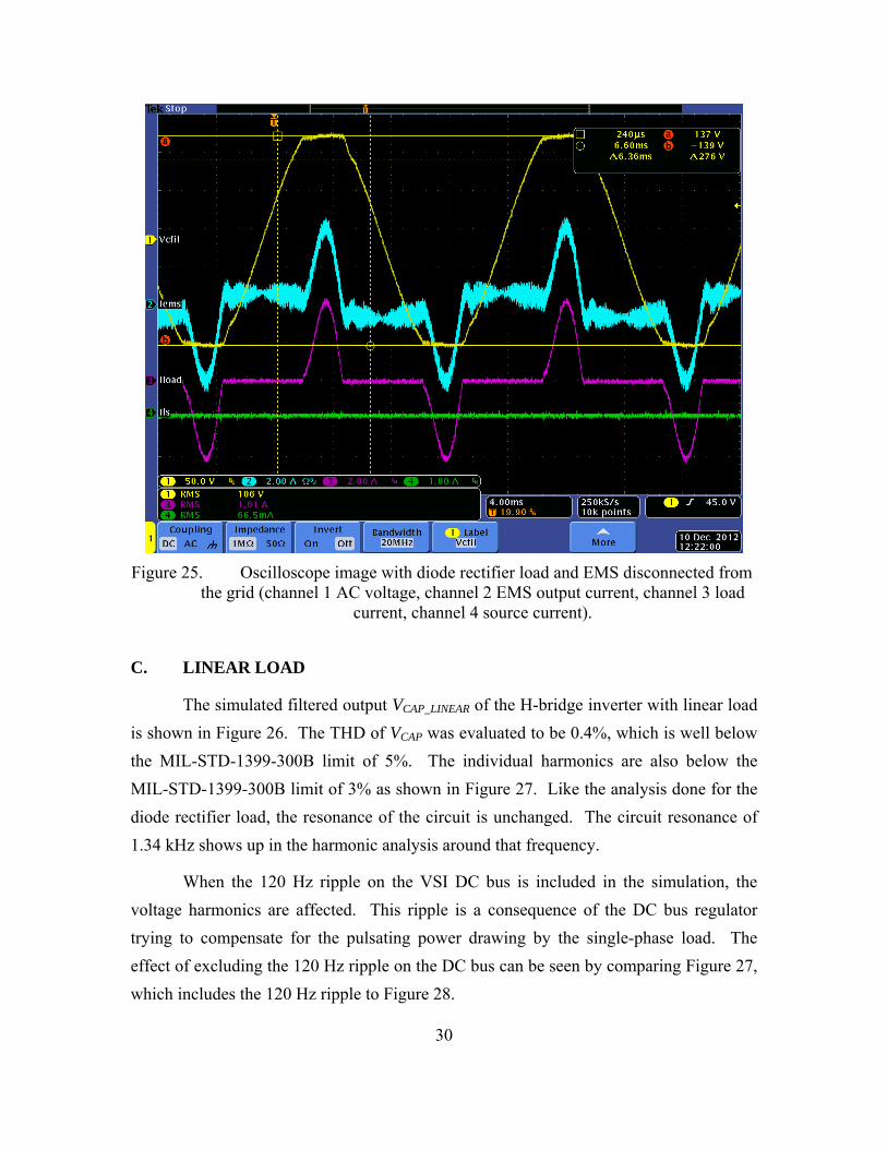
An image of the laboratory scope is shown in Figure 25. The labeled waveform
Vcfil is the voltage across capacitor C1 (labeled VCAP in Figure 10), while Iems is the
current supplied from the H-bridge inverter (labeled IH in Figure 10), and Iload is the
current supplied to the diode rectifier (labeled IS in Figure 10). The flat-topped waveform
Vcfil is due to the charging of capacitor CDC. When the load RLOAD is reduced, the
amount of flat-topping is also reduced.
Utilizing a Tektronix model MSO 4034 oscilloscope’s data acquisition feature,
we were able to import this data into MATLAB for display and harmonic analysis. The

26
imported voltage waveform across capacitor C1 which closely resembles that of the
simulation results is shown in Figure 20. The THD of VCAP was evaluated to be 4.7%.
There is also a large third order harmonic evaluated to be 3.48%, which can be seen in
Figure 21. It is also noted that the harmonics of the simulation dropped more quickly
with frequency, which was attributed to many non-ideal conditions such as voltage drop
across diode, rise and fall time of the IGBT switching, and voltage drop across the IGBTs
not being properly accounted for. However, the amplitude of all of the higher order
harmonics are still very small in the laboratory results
The THD for both the model and laboratory test was only slightly below the 5%
MIL-STD-1399-300B limit. Evaluation of the individual harmonics resulted in the third
order harmonic from the laboratory exceeding the 3% individual harmonic limit of MIL-
STD-1399-300B.
Figure 20. Simulated and measured H-bridge output filtered voltage with rectifier load.
27
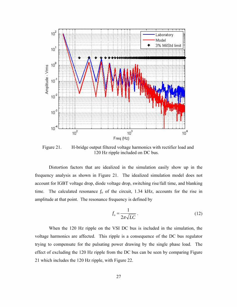
Figure 21. H-bridge output filtered voltage harmonics with rectifier load and 120 Hz ripple included on DC bus.
Distortion factors that are idealized in the simulation easily show up in the
frequency analysis as shown in Figure 21. The idealized simulation model does not
account for IGBT voltage drop, diode voltage drop, switching rise/fall time, and blanking
time. The calculated resonance fo of the circuit, 1.34 kHz, accounts for the rise in
amplitude at that point. The resonance frequency is defined by
1
2of
LC . (12)
When the 120 Hz ripple on the VSI DC bus is included in the simulation, the
voltage harmonics are affected. This ripple is a consequence of the DC bus regulator
trying to compensate for the pulsating power drawing by the single phase load. The
effect of excluding the 120 Hz ripple from the DC bus can be seen by comparing Figure
21 which includes the 120 Hz ripple, with Figure 22.

28
Figure 22. H-bridge output filtered voltage harmonics with rectifier load and 120 Hz ripple excluded on DC bus.
The load current Is is shown in Figure 23. The current pulses correspond to the
flat-topped voltage waveform of Figure 20 as the rectifier draws current when the voltage
of capacitor CDC is less than the voltage across capacitor C1. Like the voltage waveform
comparison, the simulation and laboratory currents are very similar.
The operation of user equipment with power ratings less than 1 kVA must be
current amplitude limited so that no individual harmonic line current or current of any
frequency above the fundamental at 60 Hz to 20 kHz exceeds the limit line set at a
magnitude of 6000/f percent of the user equipment’s full load fundamental current, where
f is the frequency [9]. The results of the laboratory and model with a load of 171 Ω are
shown in Figure 24. The simulated load was reduced to 70 Ω, at which point the model
showed a third voltage harmonic above the 3% limit. Analysis of the individual line
currents proved to remain out of specification for this design.

29
Figure 23. Simulated and measured H-bridge output rectifier load current.
Figure 24. Individual harmonic line currents with rectifier load.
30
Figure 25. Oscilloscope image with diode rectifier load and EMS disconnected from the grid (channel 1 AC voltage, channel 2 EMS output current, channel 3 load
current, channel 4 source current).
C. LINEAR LOAD
The simulated filtered output VCAP_LINEAR of the H-bridge inverter with linear load
is shown in Figure 26. The THD of VCAP was evaluated to be 0.4%, which is well below
the MIL-STD-1399-300B limit of 5%. The individual harmonics are also below the
MIL-STD-1399-300B limit of 3% as shown in Figure 27. Like the analysis done for the
diode rectifier load, the resonance of the circuit is unchanged. The circuit resonance of
1.34 kHz shows up in the harmonic analysis around that frequency.
When the 120 Hz ripple on the VSI DC bus is included in the simulation, the
voltage harmonics are affected. This ripple is a consequence of the DC bus regulator
trying to compensate for the pulsating power drawing by the single-phase load. The
effect of excluding the 120 Hz ripple on the DC bus can be seen by comparing Figure 27,
which includes the 120 Hz ripple to Figure 28.

31
Figure 26. Simulated and measured H-bridge output filtered voltage with linear load.
Like the output voltage shown in Figure 26, the load current drawn by Rload
closely matches that of the developed physics-based model as shown in Figure 29.
The operation of user equipment with power ratings less than 1 kVA must be
current amplitude limited so that no individual harmonic line current or current of any
frequency above the fundamental at 60 Hz to 20 kHz exceeds the limit line set at a
magnitude of 6000/f percent of the user equipment’s full load fundamental current, where
f is the frequency [9]. The results of the laboratory and model with a load of 171 Ω are
shown in Figure 30. All individual harmonic line currents remained less than 10%.
However, the laboratory results showed an out-of-specification condition near the 15 kHz
switching frequency. This was determined to be from the non-ideal source, as one would
not expect to have current line harmonics from an ideal source. MIL-STD-1399-300B
has much tighter specifications on loads than it does power sources, as the output voltage
from the VSI is within specification. Figure 31 is a screen capture of the oscilloscope
display during lab testing.

32
Figure 31 is a screen capture of the oscilloscope display during lab testing. The
labeled waveform Vcfil is the voltage across capacitor C1 (labeled VCAP_LINEAR in Figure
11), while Iems is the current supplied from the H-bridge inverter (labeled IH in Figure
11), and Iload is the current supplied to the linear load (labeled IS_linear in Figure 11).
Again, utilizing the scope’s data acquisition feature, we were able to import this data into
MATLAB for display and harmonic analysis. The imported voltage waveform across
capacitor C1 which closely resembles that of the simulation results, is shown in Figure
26. The THD of VCAP was evaluated to be 0.8%. The individual harmonics obtained in
the lab shown in Figure 26 are all below the 3% MIL-STD-1399-300B limit.
Figure 27. H-bridge output filtered voltage harmonics with linear load and 120 Hz ripple included on DC bus.

33
Figure 28. H-bridge output filtered voltage harmonics with linear load and 120 Hz ripple excluded on DC bus.
Figure 29. Simulated and measured H-bridge output linear load current.

34
Figure 30. Individual harmonic line currents with linear load.
Figure 31. Oscilloscope Image with linear load and EMS disconnected from the grid (channel 1 AC voltage, channel 2 EMS output current, channel 3 load current,
channel 4 source current).

35
VI. SIMULATION OF DIFFERENT LINEAR LOADS
A. INTRODUCTION
Through simulation and lab verification discussed in chapters IV and V, it was
shown that a passive diode rectifier load supplied by a H-bridge inverter does not meet
MIL-STD-1399-300B. However, the linear load simulated and lab verified as discussed
in Chapter V was within specification. In this chapter, the effect of higher linear loading
conditions is presented along with a simple control strategy to account for the voltage
sagging encountered.
B. LINEAR LOADING EFFECTS
The linear load portion of the model shown in Figure 12 was modified and is
pictured in Figure 32. By measuring the RMS input voltage to the linear load, a PI
controller is able to adjust the duty cycle to maintain a constant output voltage level. The
PI controller was connected to the EMS by modifying the circuit in Figure 11 to that
shown in Figure 33.
Figure 32. H-bridge model with linear load and controller.

36
Figure 33. Connection of a PI controller to the EMS.
To demonstrate the need of a controller, the output voltage was simulated by
increasing the linear load. The effects of the increased load with constant duty cycle are
shown Figure 34. The peak output voltage sags as the load increases, and therefore, the
RMS voltage sags. The RMS voltage is one of the simplest electrical power
measurements to take. Therefore, a simple PI controller that measures the RMS output
voltage and compares it to a reference was modeled as shown in Figure 32.
The PI controller regulates the output voltage by adjusting the duty cycle in order
to maintain the output voltage constant. The simulated output voltage for a 25 Ω linear
load with fixed and controlled duty cycle is shown in Figure 35. The controller increases
the duty cycle to adjust for the increased load in order to maintain the reference value
programmed. A load of 5 Ω or more resulted in a 100% duty cycle, at which time any
further load increase has unavoidable voltage sag. A higher DC input bus voltage to the
H-bridge is required for any increased loading once the duty cycle reached 100%.

37
Figure 34. Simulated output voltage comparison with linear loads and constant duty cycle.
Figure 35. Simulated output voltage comparison with and without controller.

38
THIS PAGE INTENTIONALLY LEFT BLANK

39
VII. CONCLUSION
A. ACCOMPLISHMENTS
An evaluation of an open loop PWM single-phase H-bridge inverter was
evaluated against MIL-STD-1399-300B in this thesis. The single-phase inverter is the
main entity that makes up the EMS and can be configured to operate in many different
scenarios through the use of a FPGA and software programming as discussed in Chapter
II. In addition to the laboratory built EMS, a Simulink model of the H-bridge inverter
with either a diode rectifier or linear load was evaluated against the physical EMS results.
The results of the model accurately predicted that of the hardware design. This is
a crucial step in moving to high level model driven design that saves time and money.
Through simulation and lab verification, the best PWM switching scheme, unipolar, was
identified. It was also realized that a constant linear load can easily be operated open-
loop while meeting MIL-STD-1399-300B, while dynamic linear loading would require a
simple closed loop control (illustrated in Figure 32) in order to maintain the RMS output
voltage due to voltage sagging at higher loads. No “wave-shaping” methods are required.
Out-of-specification line current harmonics with the EMS supplying a linear load
were determined to be coming from the power source (VSI) itself. Even though the
source was within specification per MIL-STD-1399-300B, it was unable to supply an
ideal load.
Evaluation of the diode rectifier load connected to an H-bridge inverter did not
meet MIL-STD-1399-300B specifications. Additional filtering would be required to
reduce the harmonics. An increased load also results in a more flat-topped voltage
waveform and higher THD to include individual harmonics. The research done in [7]
and simulated in our model proves that active filtering is a non-ideal method to correct
for this distortion with a passive diode rectifier load due to excessive diode current as
seen in Figure 36.
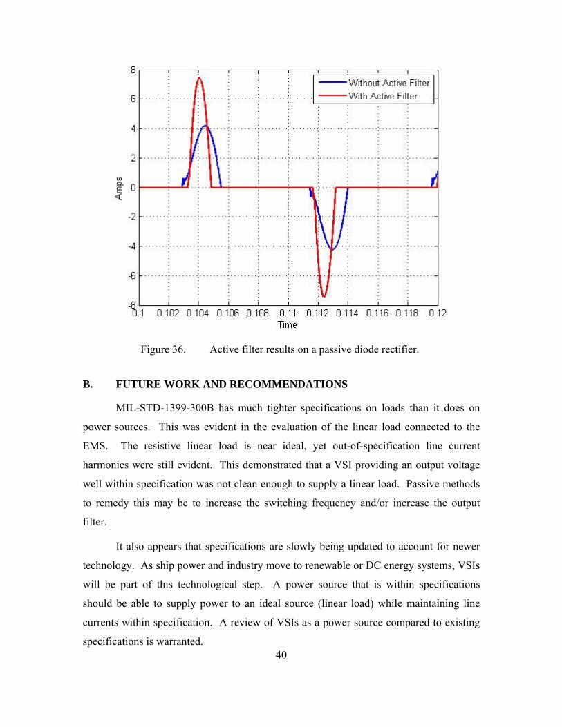
40
Figure 36. Active filter results on a passive diode rectifier.
B. FUTURE WORK AND RECOMMENDATIONS
MIL-STD-1399-300B has much tighter specifications on loads than it does on
power sources. This was evident in the evaluation of the linear load connected to the
EMS. The resistive linear load is near ideal, yet out-of-specification line current
harmonics were still evident. This demonstrated that a VSI providing an output voltage
well within specification was not clean enough to supply a linear load. Passive methods
to remedy this may be to increase the switching frequency and/or increase the output
filter.
It also appears that specifications are slowly being updated to account for newer
technology. As ship power and industry move to renewable or DC energy systems, VSIs
will be part of this technological step. A power source that is within specifications
should be able to supply power to an ideal source (linear load) while maintaining line
currents within specification. A review of VSIs as a power source compared to existing
specifications is warranted.

41
The Simulink model used was mostly ideal with some factors taken into account
like the 2.5 V 120 Hz loading pulsation found on the DC bus supplying the H-bridge.
Further modeling of individual components such as the diodes and IGBTs can be worked
into the model to achieve a higher accuracy. Furthermore, with research showing that
active filtering as a non-ideal method in correcting distortion for a diode rectifier load,
the use of a power factor correction (PFC) converter may be the answer to control
distortion in the EMS. A bridgeless pseudo-boost PFC converter is analyzed in [8] but
does not evaluate the THD. Modeling this converter, to include lab verification, would
be the next recommended step in evaluating the islanding mode of the EMS.

42
THIS PAGE INTENTIONALLY LEFT BLANK

43
APPENDIX–MATLAB CODE
% LT Andrew Metzcus % H-bridge Inverter analysis from an Energy Management System (EMS). % % This file accomplishes the follwing: % Acuisition of exported data from the oscilloscope connected to the EMS, % and plots it versus time. % This file requires the Hbridge_AnalysisModel.mdl to be ran first as it: % anyalyzes the simulation results and compares it to that of the % physical data exported from the oscilloscope. %%%%%%%%%%%%%%%%%%%%%%%%%%%%%%%%%%%%%%%%%%%%%%%%%%%%%%%%%%%%%%%%%%%%%%%%% % % DIODE LOAD % % %%%%%%%%%%%%%%%%%%%%%%%%%%%%%%%%%%%%%%%%%%%%%%%%%%%%%%%%%%%%%%%%%%%%%%%%% data_xls=xlsread('Tek_CH1_Wfm.csv'); len = length(data_xls); data=data_xls(15:len,1:2); newlen=length(data); %this equals 10,000 rows col_1-time col_2-vout time_vec=data(:,1); %column 1 only from xls - time data_vec=data(:,2); %column 2 only from xls - vout time_vec=time_vec+.0677; Fs=250e3; %sampling frequency from oscope T=.01647; len2=round(Fs*T); k=0:len2-1; freq=k/T; freqDomain=fft(data_vec(1:len2))/len2; Vrms_freqDomain= 2*abs(freqDomain(1:len2)/sqrt(2)); figure(1); plot(time_vec,data_vec,'LineWidth',2); title('Data set from Scope: Output voltage - Diode Rectifier Load'); xlabel('Time'); ylabel('Volts'); axis([.065 .092 -150 150]); grid on figure(2) IHDlimit=0.03*Vrms_freqDomain(2); %MilStd limit for IHD is 3% loglog(freq(2:len2),Vrms_freqDomain(2:len2),'bo',freq(3:len2),IHDlimit,'kx','LineWidth',2); axis([50 40000 .01 200]) xlabel('Freq (Hz)');ylabel('Amplitude - Vrms'); title('Harmonics with Diode Rectifier Load'); legend('Individual Harmonic levels','3% MilStd limit');

44
grid on % %THD calculation THDdata=Vrms_freqDomain(3:30); %2nd through 29th harmonic --(1) is DC (2) is 60Hz THDsquare=THDdata.*THDdata; THDsum=sum(THDsquare); THD=sqrt(THDsum)/Vrms_freqDomain(2) figure(3) idata_xls=xlsread('Tek_CH3_Wfm.csv'); ilen = length(idata_xls); idata=idata_xls(15:ilen,1:2); inewlen=length(idata); %this equals 10,000 rows col_1-time col_2-vout itime_vec=idata(:,1); %column 1 only from xls - time idata_vec=idata(:,2); %column 2 only from xls - load current itime_vec=itime_vec+.0677; plot(itime_vec,idata_vec,'LineWidth',2); title('Load Current - Is'); xlabel('Time'); ylabel('Amps'); axis([.065 .092 -5 5]); grid on % %THD calculation- Current ifreqDomain=fft(idata_vec(1:len2))/len2; Irms_freqDomain= 2*abs(ifreqDomain(1:len2)/sqrt(2)); iTHDdata=Irms_freqDomain(3:30); %2nd through 29th harmonic --(1) is DC (2) is 60Hz iTHDsquare=iTHDdata.*iTHDdata; iTHDsum=sum(iTHDsquare); iTHD=sqrt(iTHDsum)/Irms_freqDomain(2) figure(4); plot(time_vec,data_vec,'LineWidth',2); title('Output voltage Comparison'); xlabel('Time'); ylabel('Volts'); axis([.065 .092 -150 150]); grid on hold on plot(time, Vcap, 'r','LineWidth',2); legend('Laboratory','Model'); figure(5) plot(itime_vec,idata_vec,'LineWidth',2); title('Load Current Comparison'); xlabel('Time'); ylabel('Amps'); axis([.065 .092 -5 5]); grid on hold on plot(time, is, 'r','LineWidth',2); legend('Laboratory','Model'); simFs=1/20/tstep; %sampling frequency from simulation

45
simlen2=round(1/60*simFs); %obtains number of samples in one cycle simk=0:simlen2-1; %create a vector from 0 to newlen-1 simT=simlen2/simFs; %get the frequency interval simfreq=simk/simT; %create the frequency range figure(6); plot(time,Vcap, 'r','LineWidth',2); title('Simulation Results: Vcap with Diode Rectifier Load'); xlabel('Time'); ylabel('Volts'); axis([.065 .092 -150 150]); grid on figure(7) plot(time, is, 'r','LineWidth',2); axis([.07 .1 -5 5]); title('Simulation Results: Load Current - Is'); xlabel('Time'); ylabel('Amps'); axis([.065 .092 -5 5]); grid on simfreqDomain=fft(Vcap((4*simlen2):(5*simlen2)))/simlen2; %fft of 4th cycle of simulation simVrms_freqDomain= 2*abs(simfreqDomain(1:simlen2)/sqrt(2)); THDsimdata=simVrms_freqDomain(3:30); %2nd through 29th harmonic --(1) is DC (2) is 60Hz THDsimsquare=THDsimdata.*THDsimdata; THDsimsum=sum(THDsimsquare); THDsim=sqrt(THDsimsum)/simVrms_freqDomain(2) figure(8) simIHDlimit=0.03*simVrms_freqDomain(2); %MilStd limit for IHD is 3% loglog(freq(2:len2),Vrms_freqDomain(2:len2),'b','linewidth',2); %Labratory hold on loglog(simfreq(2:simlen2),simVrms_freqDomain(2:simlen2),'r','linewidth',2);%sim Unipolar loglog(simfreq(3:simlen2),simIHDlimit,'k*','LineWidth',2); % "3%" MIL-STD-1399-300A limit title('Voltage Harmonic Comparison'); axis([50 10000 .0001 200]) xlabel('Freq (Hz)');ylabel('Amplitude - Vrms'); title('Voltage Harmonic Comparison'); legend('Laboratory','Model','3% MilStd limit'); grid on hold off sz=size(freq); freq1=ones(sz); freq1=6000.*freq1; freqlimit=freq1./freq; Irms_freq_percent=Irms_freqDomain./Irms_freqDomain(2).*100;

46
isimfreqDomain=fft(is((4*simlen2):(5*simlen2)))/simlen2; %fft of 4th cycle of simulation simIrms_freqDomain= 2*abs(isimfreqDomain(1:simlen2)/sqrt(2)); simIrms_freq_percent=simIrms_freqDomain./simIrms_freqDomain(2).*100; iTHDsimdata=simIrms_freqDomain(3:30); %2nd through 29th harmonic --(1) is DC (2) is 60Hz iTHDsimsquare=iTHDsimdata.*iTHDsimdata; iTHDsimsum=sum(iTHDsimsquare); iTHDsim=sqrt(iTHDsimsum)/simIrms_freqDomain(2); figure(10) semilogx(freq(3:len2),Irms_freq_percent(3:len2),'bo','linewidth',2); %Labratory grid on hold on semilogx(simfreq(3:len2),simIrms_freq_percent(3:len2),'rd','linewidth',2); semilogx(simfreq(2:len2),freqlimit(2:len2),'k','LineWidth',2); %MIL-STD-1399-300B limit title('Harmonic Line Current Comparison with diode rectifier load'); axis([10 20000 0 100]) xlabel('Freq (Hz)');ylabel('% of 60Hz Fundamental Current (A)'); legend('Laboratory','Model',sprintf('MilStd limit: 60Hz user\n equipment <1kVA')); grid on hold off %%%%%%%%%%%%%%%%%%%%%%%%%%%%%%%%%%%%%%%%%%%%%%%%%%%%%%%%%%%%%%%%%%%%%%%%%%%%%%%%%%%%%%%% %Code Below is for showing how unipolar has the effect of doubling the %switching frequency %%%%%%%%%%%%%%%%%%%%%%%%%%%%%%%%%%%%%%%%%%%%%%%%%%%%%%%%%%%%%%%%%%%%%%%%%%%%%%%%%%%%%%%% % figure(11) % loglog(simfreq(2:simlen2),simVrms_freqDomain(2:simlen2),'b','linewidth',6);%sim Unipolar % hold on % loglog(simfreq(2:simlen2),simVrms_freqDomainbi(2:simlen2),'r','linewidth',2);%sim Bipolar % loglog(simfreq(3:simlen2),simIHDlimit,'k*'); % "3%" MIL-STD-1399-300A limit % title('Unipolar vs Bipolar Simulation Comparison - Voltage Harmonics'); % legend('Unipolar','Bipolar','3% MilStd limit'); % axis([50 40000 .0001 200]) % xlabel('Freq (Hz)');ylabel('Amplitude - Vrms'); % grid on % hold off %%%%%%%%%%%%%%%%%%%%%%%%%%%%%%%%%%%%%%%%%%%%%%%%%%%%%%%%%%%%%%%%%%%%%%%%%%%%%%%%%%%%% %

47
% The Code Below is for the analysis of the Linear Load % %%%%%%%%%%%%%%%%%%%%%%%%%%%%%%%%%%%%%%%%%%%%%%%%%%%%%%%%%%%%%%%%%%%%%%%%%%%%%%%%%%%%% data_xls=xlsread('Tek_CH1_Wfm_linear.csv'); len = length(data_xls); data=data_xls(15:len,1:2); newlen=length(data); %this equals 10,000 rows col_1-time col_2-vout time_vec=data(:,1); %column 1 only from xls - time data_vec=data(:,2); %column 2 only from xls - vout time_vec=time_vec+.0677; Fs=250e3; %sampling frequency from oscope T=.01647; len2=round(Fs*T); k=0:len2-1; freq=k/T; freqDomain=fft(data_vec(1:len2))/len2; Vrms_freqDomain= 2*abs(freqDomain(1:len2)/sqrt(2)); figure(12) idata_xls=xlsread('Tek_CH3_Wfm_linear.csv'); ilen = length(idata_xls); idata=idata_xls(15:ilen,1:2); inewlen=length(idata); %this equals 10,000 rows col_1-time col_2-vout itime_vec=idata(:,1); %column 1 only from xls - time idata_vec=idata(:,2); %column 2 only from xls - load current itime_vec=itime_vec+.0677; plot(itime_vec,idata_vec,'LineWidth',2); title('Load Current - Is'); xlabel('Time'); ylabel('Amps'); axis([.065 .092 -5 5]); grid on % %THD calculation- Current ifreqDomain=fft(idata_vec(1:len2))/len2; Irms_freqDomain= 2*abs(ifreqDomain(1:len2)/sqrt(2)); iTHDdata=Irms_freqDomain(3:30); %2nd through 29th harmonic --(1) is DC (2) is 60Hz iTHDsquare=iTHDdata.*iTHDdata; iTHDsum=sum(iTHDsquare); iTHD=sqrt(iTHDsum)/Irms_freqDomain(2) figure(13); plot(time_vec,data_vec,'LineWidth',2); title('Output voltage - Linear Load'); xlabel('Time'); ylabel('Volts'); axis([.065 .092 -150 150]); grid on figure(14)

48
IHDlimit=0.03*Vrms_freqDomain(2); %MilStd limit for IHD is 3% loglog(freq(2:len2),Vrms_freqDomain(2:len2),'bo',freq(3:len2),IHDlimit,'kx','LineWidth',2); axis([50 20000 .01 200]) xlabel('Freq (Hz)');ylabel('Amplitude - Vrms'); title('Harmonics with Linear Load'); legend('Individual Harmonic levels','3% MilStd limit'); grid on % %THD calculation THDdata=Vrms_freqDomain(3:30); %2nd through 29th harmonic --(1) is DC (2) is 60Hz THDsquare=THDdata.*THDdata; THDsum=sum(THDsquare); THD=sqrt(THDsum)/Vrms_freqDomain(2) figure(15) idata_xls=xlsread('Tek_CH3_Wfm_linear.csv'); ilen = length(idata_xls); idata=idata_xls(15:ilen,1:2); inewlen=length(idata); %this equals 10,000 rows col_1-time col_2-vout itime_vec=idata(:,1); %column 1 only from xls - time idata_vec=idata(:,2); %column 2 only from xls - load current itime_vec=itime_vec+.0677; plot(itime_vec,idata_vec,'LineWidth',2); title('Load Current with Linear Load'); xlabel('Time'); ylabel('Amps'); axis([.065 .092 -1 1]); grid on figure(16); plot(time_vec,data_vec,'LineWidth',2); title('Output voltage Comparison with Linear Load'); xlabel('Time'); ylabel('Volts'); axis([.065 .092 -150 150]); grid on hold on plot(time, Vcap_linear, 'r','LineWidth',2); legend('Laboratory','Model'); figure(17) plot(itime_vec,idata_vec,'LineWidth',2); hold on plot(time, Is_linear, 'r','LineWidth',2); title('Load Current Comparison with Linear Load'); xlabel('Time'); ylabel('Amps'); axis([.065 .092 -1 1]); grid on legend('Laboratory','Model'); hold off simFs=1/20/tstep; %sampling frequency from simulation simlen2=round(1/60*simFs); %obtains number of samples in one cycle simk=0:simlen2-1; %create a vector from 0 to newlen-1

49
simT=simlen2/simFs; %get the frequency interval simfreq=simk/simT; %create the frequency range figure(18); plot(time,Vcap_linear, 'r','LineWidth',2); title('Simulation Results: Vcap with Linear Load'); xlabel('Time'); ylabel('Volts'); axis([.065 .092 -150 150]); grid on figure(19) plot(time, Is_linear, 'r','LineWidth',2); axis([.07 .1 -5 5]); title('Simulation Results: Load Current with Linear Load'); xlabel('Time'); ylabel('Amps'); axis([.065 .092 -1 1]); grid on simfreqDomain=fft(Vcap_linear((4*simlen2):(5*simlen2)))/simlen2; %fft of 4th cycle of simulation simVrms_freqDomain= 2*abs(simfreqDomain(1:simlen2)/sqrt(2)); THDsimdata=simVrms_freqDomain(3:30); %2nd through 29th harmonic --(1) is DC (2) is 60Hz THDsimsquare=THDsimdata.*THDsimdata; THDsimsum=sum(THDsimsquare); THDsim=sqrt(THDsimsum)/simVrms_freqDomain(2) figure(20) simIHDlimit=0.03*simVrms_freqDomain(2); %MilStd limit for IHD is 3% loglog(freq(2:len2),Vrms_freqDomain(2:len2),'b','LineWidth',2); hold on loglog(simfreq(2:simlen2),simVrms_freqDomain(2:simlen2),'r','LineWidth',2); loglog(simfreq(3:simlen2),simIHDlimit,'k*','LineWidth',2); axis([50 10000 .0001 200]) xlabel('Freq (Hz)');ylabel('Amplitude - Vrms'); title('Voltage Harmonic Comparison with Linear Load'); legend('Laboratory','Model','3% MilStd limit'); grid on hold off sz=size(freq); freq1=ones(sz); freq1=6000.*freq1; freqlimit=freq1./freq; Irms_freq_percent=Irms_freqDomain./Irms_freqDomain(2).*100; isimfreqDomain=fft(Is_linear((4*simlen2):(5*simlen2)))/simlen2; %fft of 4th cycle of simulation simIrms_freqDomain= 2*abs(isimfreqDomain(1:simlen2)/sqrt(2)); simIrms_freq_percent=simIrms_freqDomain./simIrms_freqDomain(2).*100;

50
iTHDsimdata=simIrms_freqDomain(3:30); %2nd through 29th harmonic --(1) is DC (2) is 60Hz iTHDsimsquare=iTHDsimdata.*iTHDsimdata; iTHDsimsum=sum(iTHDsimsquare); iTHDsim=sqrt(iTHDsimsum)/simIrms_freqDomain(2); figure(21) semilogx(freq(3:len2),Irms_freq_percent(3:len2),'bo','linewidth',2); %Laboratory grid on hold on semilogx(simfreq(3:len2),simIrms_freq_percent(3:len2),'rd','linewidth',2); simIrms_freq_percent_orig=simIrms_freq_percent; semilogx(simfreq(2:len2),freqlimit(2:len2),'k','LineWidth',2); %MIL-STD-1399-300B limit title('Harmonic Line Current Comparison with Linear Load'); axis([10 20000 0 10]) xlabel('Freq (Hz)');ylabel('% of 60Hz Fundamental Current (A)'); legend('Laboratory','Model',sprintf('MilStd limit: 60Hz user\n equipment <1kVA')); grid on hold off figure(22) [haxes,hline1,hline2] = plotyy(time,Vcap,time,is); axes(haxes(1)) axis([.065 .092 -160 160]) ylabel('Volts'); set(hline1,'Color','b','LineWidth',2) grid on axes(haxes(2)) set(hline2,'Color','r','LineWidth',2) axis([.065 .092 -8 8]) ylabel('Amps'); xlabel('Time'); grid on legend('Current','Voltage'); set(haxes,'ycolor','b';'r') title('Simulated Voltage and Current w/o Active Filter') figure(23) [haxes,hline1,hline2] = plotyy(time,Vcap_active,time,is_active); axes(haxes(1)) axis([.065 .092 -160 160]) ylabel('Volts'); set(hline1,'Color','b','LineWidth',2) grid on set(gca,'YTick',[-150 -100 -50 0 50 100 150]) axes(haxes(2)) set(hline2,'Color','r','LineWidth',2)

51
axis([.065 .092 -8 8]) ylabel('Amps'); xlabel('Time'); grid on legend('Current','Voltage'); set(gca,'YTick',[-6 -4 -2 0 2 4 6]) set(haxes,'ycolor','b';'r') title('Simulated Voltage and Current w/ Active Filter')

52
THIS PAGE INTENTIONALLY LEFT BLANK

53
LIST OF REFERENCES
[1] Office of Naval Research. (2009 October). Naval energy–A strategic approach [Online]. Available: http://www.onr.navy.mil/naval-energy-forum/~/media/Files/Conferences/Naval%20Energy%20Forum/Naval%20Energy%20Strategy%20overview.ashx
[2] Shore Energy Management, OPNAVINST 4100.5E, June 22, 2012.
[3] G. Oriti, A. L. Julian, and N.J. Peck, “Power electronics enabled energy management systems,” in Proc. of IEEE Applied Power Electronics Conf. (APEC), Long Beach, CA, Mar., 2013.
[4] F.Z. Peng, Y.W. Li, and L.M. Tolbert, “Control and protection of power electronics interfaced distributed generation systems in a customer-driven microgrid,” in Proc. of IEEE Power and Energy Society General Meeting, Calgary, AB, Canada, pp. 1–8, July 2009.
[5] Wikipedia, s.v. “Field programmable gate arrays,” last modified May 21, 2013, http://en.wikipedia.org/wiki/FPGA [Accessed: June 3, 2013].
[6] N. Mohan and T. Undeland, W. P. Robbins, Power Electronics, Converters Applications and Design, (3rd edition), New York: John Wiley and Sons, 2003.
[7] J.G. Pinto, P. Neves, R. Pregitzer, L. F. C. Monteiro, and J L. Afonso, “Single-phase shunt active filter with digital control,” at International Conference on Renewable Energies and Power Quality (ICREPQ’07), Seville, Spain, March 2007.
[8] Z. Chen, J. Xu, F. Zhang, “Analysis of bridgeless pseudo-boost PFC converter,” in Proc. of IEEE International Symposium on Industrial Electronics, Hangzhou, China, pp. 189–193, May 2012
[9] DOD Interface Standard Section 300B Electric Power, Alternating Current, MIL-STD-1399-300B, April 24, 2008.

54
THIS PAGE INTENTIONALLY LEFT BLANK

55
INITIAL DISTRIBUTION LIST
1. Defense Technical Information Center Ft. Belvoir, Virginia 2. Dudley Knox Library Naval Postgraduate School Monterey, California