hc20.24.140.system architecture implications and … architecture implications and perspective hot...
TRANSCRIPT
1
High Bandwidth Memory Technology:
System Architecture Implications and Perspective
Hot Chips 2008
Fritz Kruger
2 2
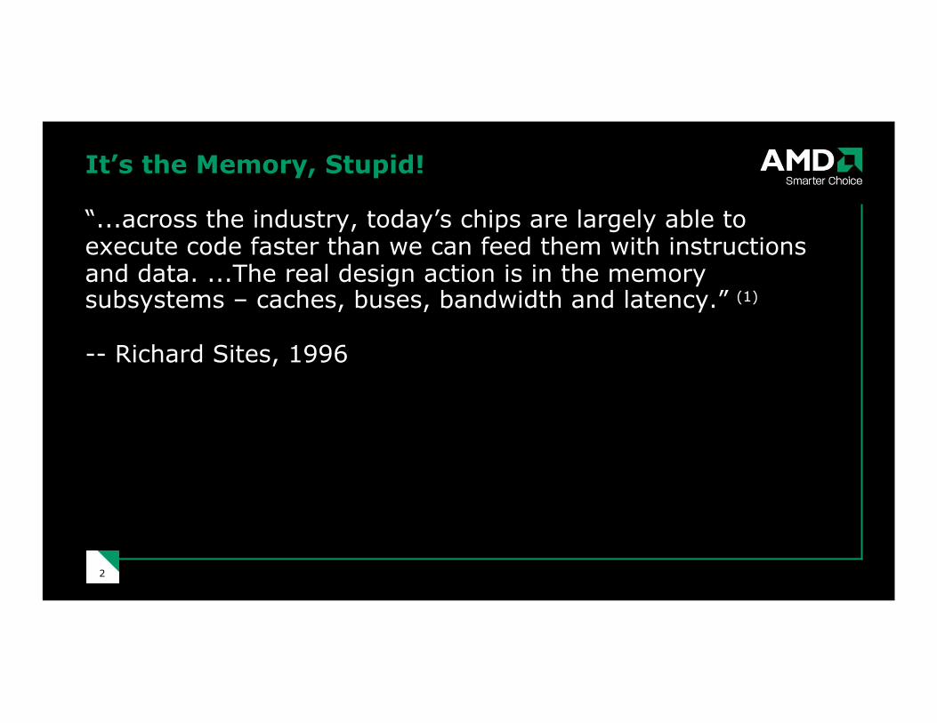
It’s the Memory, Stupid!
“...across the industry, today’s chips are largely able to execute code faster than we can feed them with instructions and data. ...The real design action is in the memory subsystems – caches, buses, bandwidth and latency.” (1)
-- Richard Sites, 1996
3 3
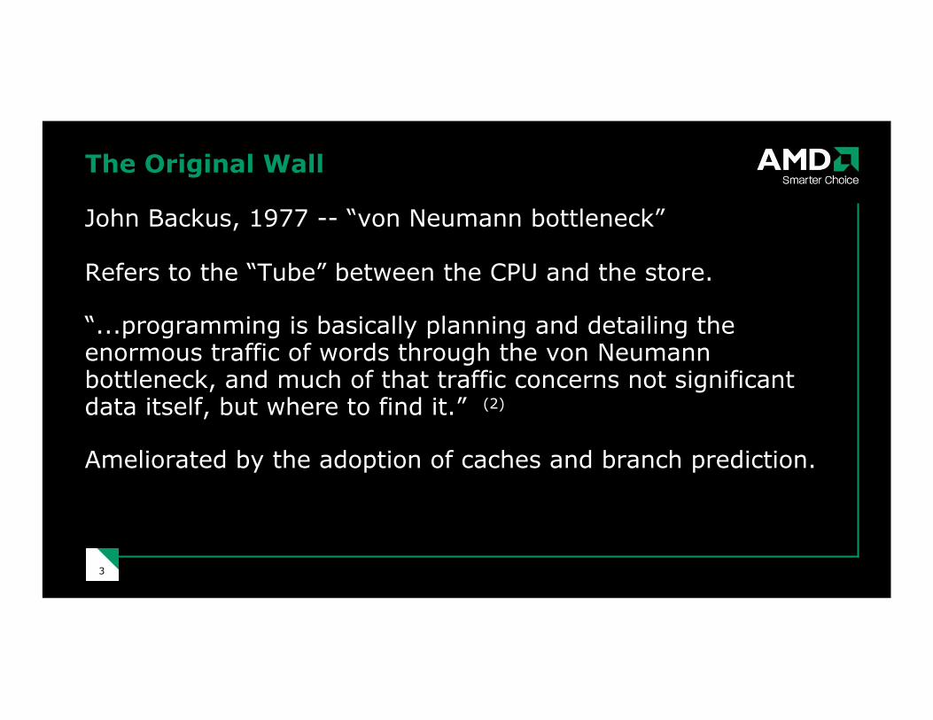
The Original Wall
John Backus, 1977 -- “von Neumann bottleneck”
Refers to the “Tube” between the CPU and the store.
“...programming is basically planning and detailing the enormous traffic of words through the von Neumann bottleneck, and much of that traffic concerns not significant data itself, but where to find it.” (2)
Ameliorated by the adoption of caches and branch prediction.
4 4
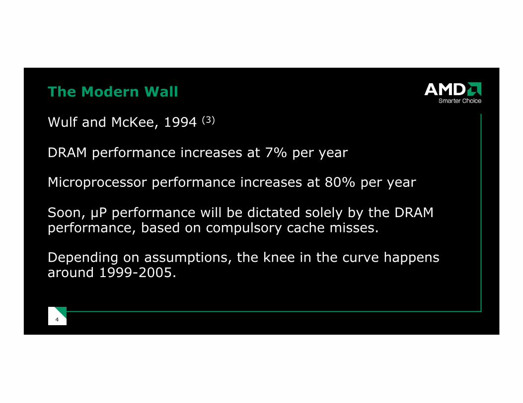
The Modern Wall
Wulf and McKee, 1994 (3)
DRAM performance increases at 7% per year
Microprocessor performance increases at 80% per year
Soon, µP performance will be dictated solely by the DRAM performance, based on compulsory cache misses.
Depending on assumptions, the knee in the curve happens around 1999-2005.
5 5
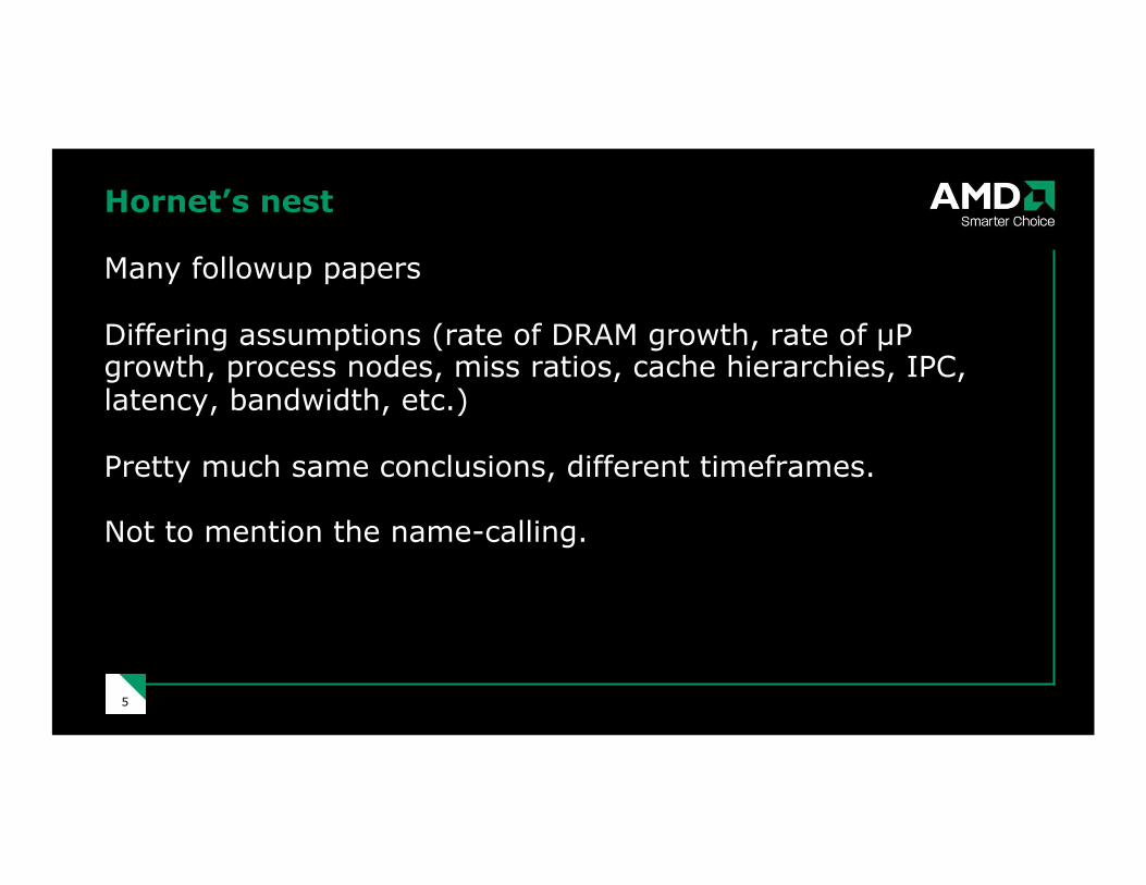
Hornet’s nest
Many followup papers
Differing assumptions (rate of DRAM growth, rate of µP growth, process nodes, miss ratios, cache hierarchies, IPC, latency, bandwidth, etc.)
Pretty much same conclusions, different timeframes.
Not to mention the name-calling.
6 6
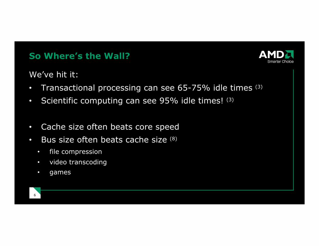
So Where’s the Wall?
We’ve hit it:
• Transactional processing can see 65-75% idle times (3)
• Scientific computing can see 95% idle times! (3)
• Cache size often beats core speed
• Bus size often beats cache size (8)
• file compression
• video transcoding
• games
7 7
Cracks in the Wall
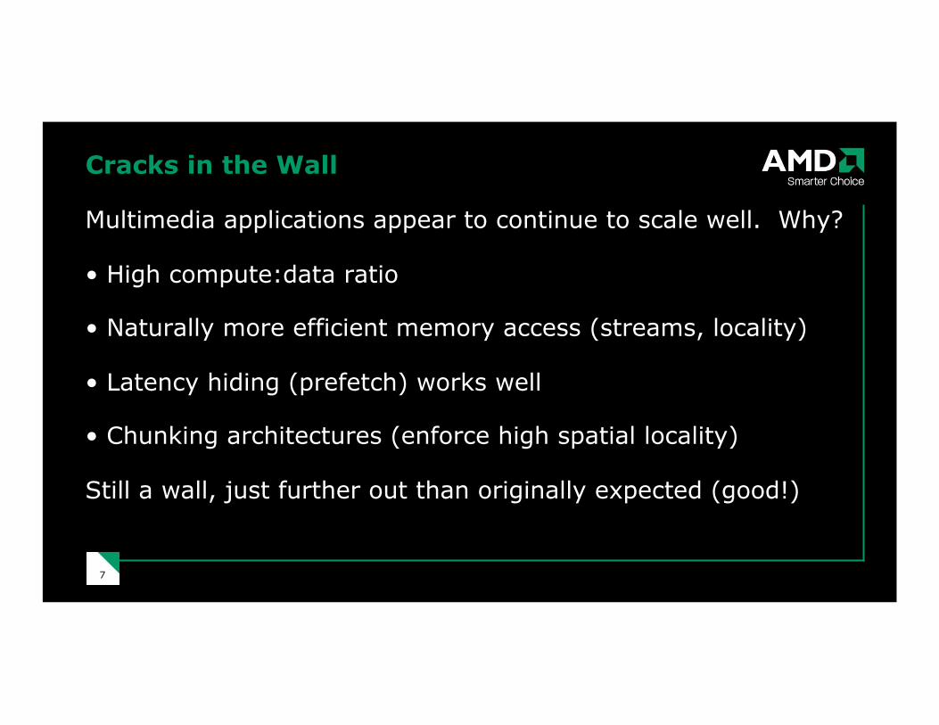
Multimedia applications appear to continue to scale well. Why?
• High compute:data ratio
• Naturally more efficient memory access (streams, locality)
• Latency hiding (prefetch) works well
• Chunking architectures (enforce high spatial locality)
Still a wall, just further out than originally expected (good!)
8 8
The GPU wall
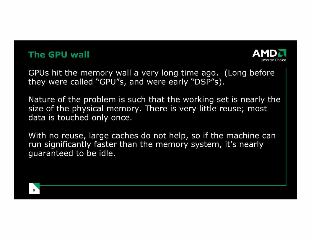
GPUs hit the memory wall a very long time ago. (Long before they were called “GPU”s, and were early “DSP”s).
Nature of the problem is such that the working set is nearly the size of the physical memory. There is very little reuse; most data is touched only once.
With no reuse, large caches do not help, so if the machine can run significantly faster than the memory system, it’s nearly guaranteed to be idle.
9 9
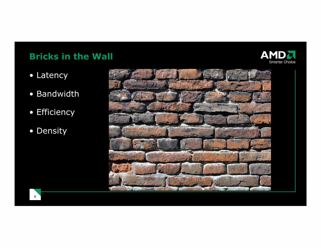
Bricks in the Wall
• Latency
• Bandwidth
• Efficiency
• Density
10 10
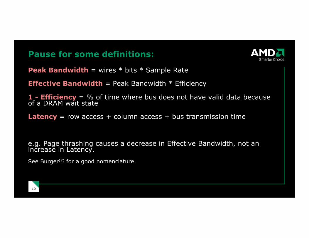
Pause for some definitions:
Peak Bandwidth = wires * bits * Sample Rate
Effective Bandwidth = Peak Bandwidth * Efficiency
1 - Efficiency = % of time where bus does not have valid data because of a DRAM wait state
Latency = row access + column access + bus transmission time
e.g. Page thrashing causes a decrease in Effective Bandwidth, not an increase in Latency.
See Burger(7) for a good nomenclature.
11 11
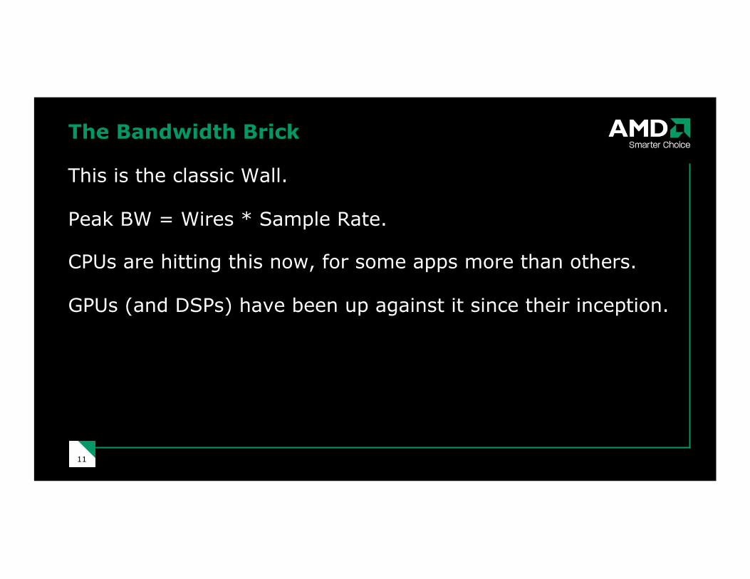
The Bandwidth Brick
This is the classic Wall.
Peak BW = Wires * Sample Rate.
CPUs are hitting this now, for some apps more than others.
GPUs (and DSPs) have been up against it since their inception.
12
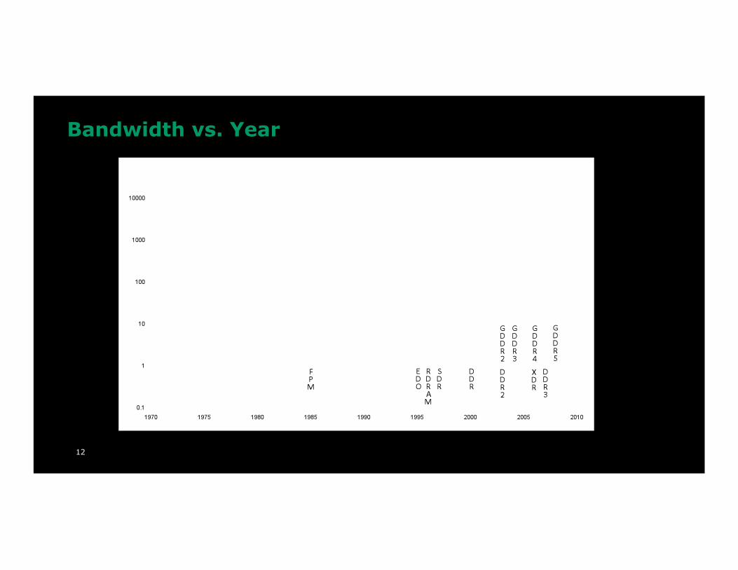
Bandwidth vs. Year
2x / 3 years
13 13
The Efficiency Brick
Effective BW = Efficiency * Peak Bandwidth.
Different than raw speed, both CPU and GPU grapple with efficiency.
Larger and more complex memory controllers, to match increasingly complex timing requirements from DRAMs.
The number and dissimilarity of request sources also continues to rise, making it even more difficult to arbitrate efficiently.
14 14
The Latency Brick
The CPU hits this in spades. Attempts to hide latency typically result in greater overfetch (e.g. speculative prefetch), so more bandwidth is needed.
But a DRAM system with higher bandwidth has a higher latency, and round and round we go, getting bigger and more power-hungry on each cycle.
The GPU (and some CPUs) work around it by having enough live threads to hide fetch latency. Cost is high in architectural register space and the difficult programming model.
15
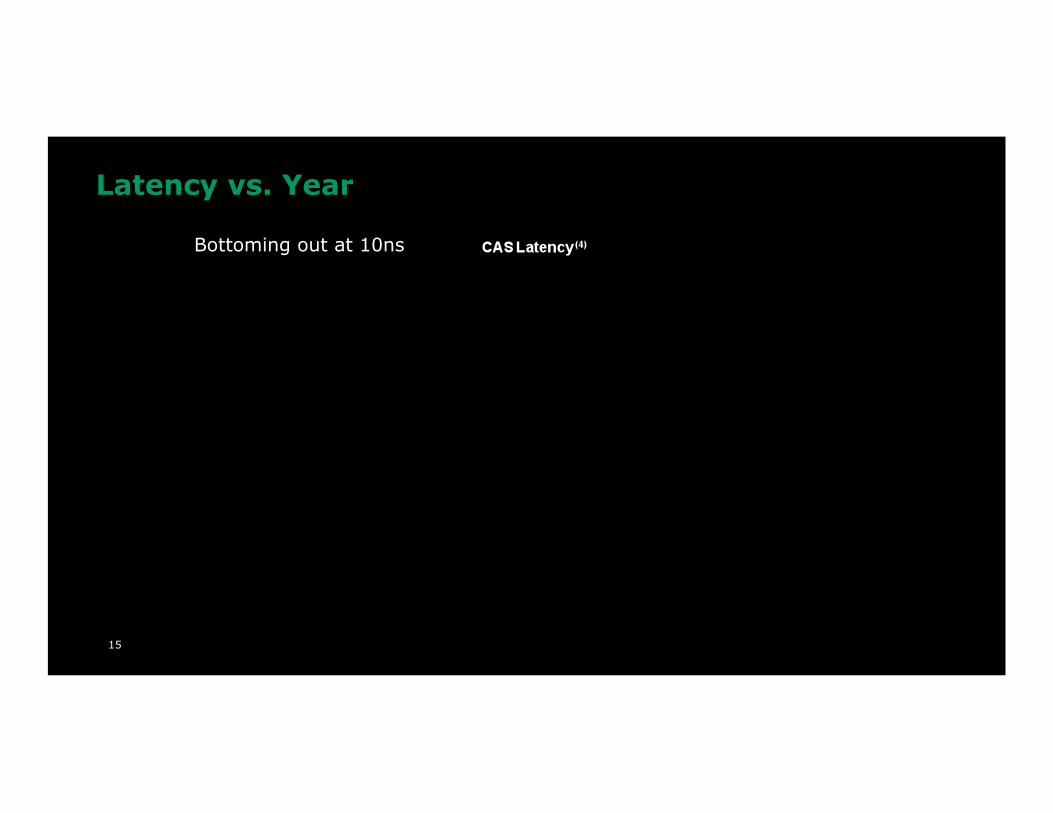
Latency vs. Year
Bottoming out at 10ns
16 16
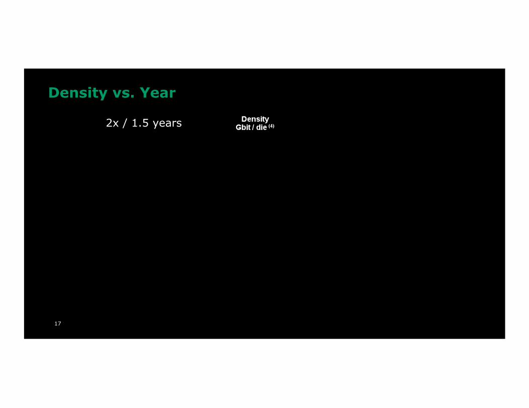
The Density Brick (Not!)
• Density has been scaling very nicely on Moore’s law, and shows no major signs of abatement.
• This is the one trend in memory that we can count on – how do we take advantage of it?
1
6
17
Density vs. Year
2x / 1.5 years
18 18
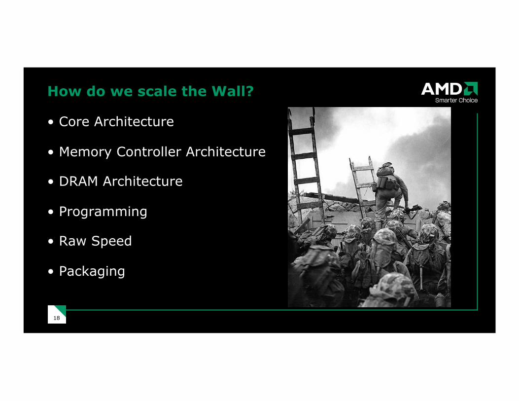
How do we scale the Wall?
• Core Architecture
• Memory Controller Architecture
• DRAM Architecture
• Programming
• Raw Speed
• Packaging
19 19
Core Architecture Scaling
• Decrease Cache miss rate
• Larger / more caches
• Higher associativity
• More threads can hide more latency; trade that for increased effective bandwidth
• Less overfetch
• More request reordering
• Fixed-function devices with memory access are equivalent to ‘threads’
• Hardware compression of common data structures
Hard for general-purpose machines, great for special-purpose machines
20 20
Memory Controller Architecture
The Wall says: if the bus is idle, you’re losing performance!
• Request Reordering
• Page Policy
• Refresh
• Read / Write Switching
• More Channels
• Prefetch
21 21
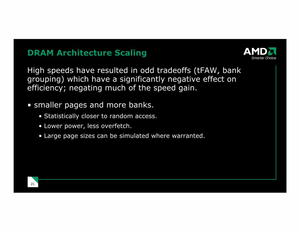
DRAM Architecture Scaling
High speeds have resulted in odd tradeoffs (tFAW, bank grouping) which have a significantly negative effect on efficiency; negating much of the speed gain.
• smaller pages and more banks.
• Statistically closer to random access.
• Lower power, less overfetch.
• Large page sizes can be simulated where warranted.
22 22
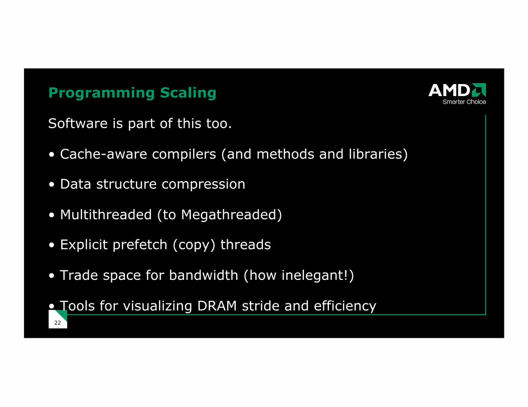
Programming Scaling
Software is part of this too.
• Cache-aware compilers (and methods and libraries)
• Data structure compression
• Multithreaded (to Megathreaded)
• Explicit prefetch (copy) threads
• Trade space for bandwidth (how inelegant!)
• Tools for visualizing DRAM stride and efficiency
23 23
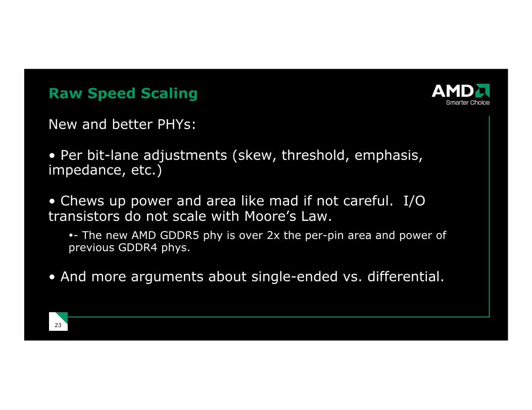
Raw Speed Scaling
New and better PHYs:
• Per bit-lane adjustments (skew, threshold, emphasis, impedance, etc.)
• Chews up power and area like mad if not careful. I/O transistors do not scale with Moore’s Law.
- The new AMD GDDR5 phy is over 2x the per-pin area and power of previous GDDR4 phys.
• And more arguments about single-ended vs. differential.
24 24
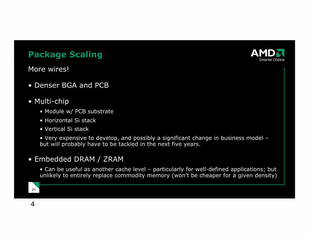
Package Scaling
More wires!
• Denser BGA and PCB
• Multi-chip
• Module w/ PCB substrate
• Horizontal Si stack
• Vertical Si stack
• Very expensive to develop, and possibly a significant change in business model – but will probably have to be tackled in the next five years.
• Embedded DRAM / ZRAM
• Can be useful as another cache level – particularly for well-defined applications; but unlikely to entirely replace commodity memory (won’t be cheaper for a given density)
2
4
25 25
Challenges in the Vertical Stack
• To make commodity, the stack footprint must be standardized.
• Low-end and high-end cores and rams will likely have the same footprint and pin drivers; so wire count and thus peak bandwidth is unlikely to scale much with market segment. Power may also not scale well for the same reason.
• Efficiency may scale with density (deeper stack = more banks); so can we regain some market segment differentiation in the memory system.
• But still, the low-end of the market will likely pay for bandwidth it can’t use. On the other hand, the low-end will be further from The Wall; so core costs could be reduced (e.g. smaller caches).
26 26
Challenges in the Vertical Stack (2)
• Through Silicon Via (TSV) must carry data and power vertically through the stack.
• Number is quite high (perhaps 4-6K), and they are not that small (perhaps 35x35µm). Hopefully the size will shrink with process generations.
• Huge challenge for physical design teams (routing logic onto Swiss cheese).
• Huge challenge for the logic design teams to deliver something to PD that they can possibly route. All the data interconnect (memory controller, TLBs, caches, etc.) will likely want to be distributed so as to reduce total wire cost and point to point latency.
– Bad enough when the I/O was a dense ring around the perimeter of the chip
– A stacked DRAM footprint will probably look something like a sparse grid over the entire chip
27 27
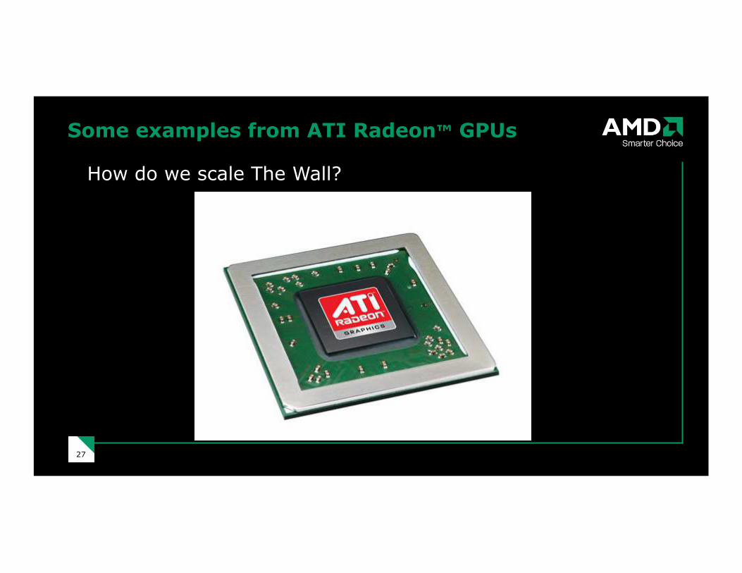
Some examples from ATI Radeon™ GPUs
How do we scale The Wall?
28 28
ATI Radeon™ GPU Core Examples
• Massively multithreaded
• Fully associative caches
• Color and Depth pre-fetch
• Texture & Depth compression
29 29
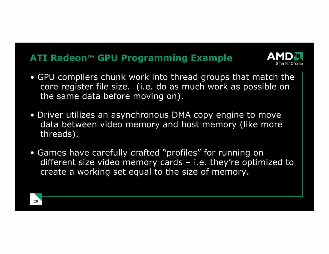
ATI Radeon™ GPU Programming Example
• GPU compilers chunk work into thread groups that match the core register file size. (i.e. do as much work as possible on the same data before moving on).
• Driver utilizes an asynchronous DMA copy engine to move data between video memory and host memory (like more threads).
• Games have carefully crafted “profiles” for running on different size video memory cards – i.e. they’re optimized to create a working set equal to the size of memory.
30 30
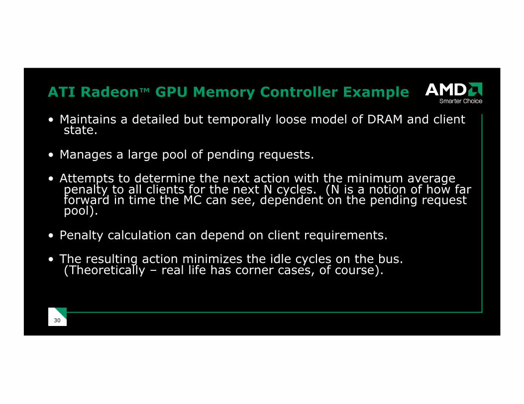
ATI Radeon™ GPU Memory Controller Example
• Maintains a detailed but temporally loose model of DRAM and client state.
• Manages a large pool of pending requests.
• Attempts to determine the next action with the minimum average penalty to all clients for the next N cycles. (N is a notion of how far forward in time the MC can see, dependent on the pending request pool).
• Penalty calculation can depend on client requirements.
• The resulting action minimizes the idle cycles on the bus. (Theoretically – real life has corner cases, of course).
31 31
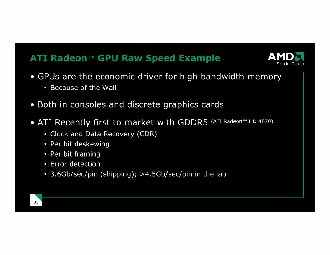
ATI Radeon™ GPU Raw Speed Example
• GPUs are the economic driver for high bandwidth memory
Because of the Wall!
• Both in consoles and discrete graphics cards
• ATI Recently first to market with GDDR5 (ATI Radeon™ HD 4870)
Clock and Data Recovery (CDR)
Per bit deskewing
Per bit framing
Error detection
3.6Gb/sec/pin (shipping); >4.5Gb/sec/pin in the lab
32 32
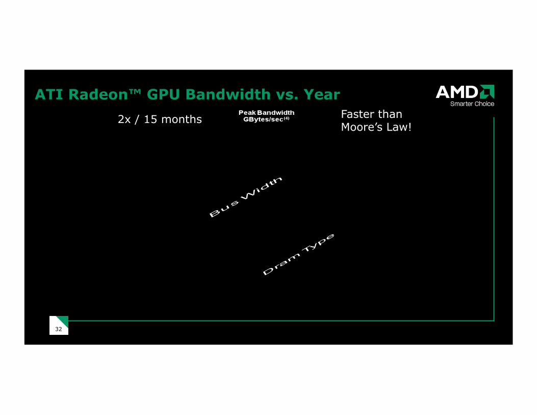
ATI Radeon™ GPU Bandwidth vs. Year
2x / 15 months Faster than Moore’s Law!
33 33
The Other Wall
Beware the I/O Wall!
The hidden assumption of the Memory Wall is that the bulk of the working set fits within main memory.
If it does not, the same arguments will apply to the I/O system (view main memory as yet another cache in the hierarchy).
Perhaps a need for yet another level of hierarchy to reduce the bottleneck for those applications
• High RPM Disks
• RAID-0
• Solid state Drives
34 34
Summary
The costs of doubling bandwidth appear to be escalating. Major investment will be needed to keep the current trend going past another five years.
So, increasingly, “The Wall” needs to be of serious consideration in every phase of design; from core and dram architecture to software.
35 35
References
1) Sites, R. It's the Memory, Stupid! Microprocessor Report, 10(10):1-2, Aug. 1996.
2) Backus, J. 1978. Can Programming Be Liberated from the von Neumann Style? A Functional Style and Its Algebra of Programs. In Communications of the ACM 21(8):613-41, Aug. 1978 *
3) McKee, S. A. 2004. Reflections on the memory wall. In Proceedings of the 1st Conference on Computing Frontiers (Ischia, Italy, April 14 - 16, 2004). CF '04. ACM, New York, NY, 162. *
4) Data gathered by the author from a variety of sources; accuracy is not guaranteed.
5) Image on page 9 is in the public domain: http://commons.wikimedia.org/wiki/Image:BrickWall.jpg
6) Image on page 18 is in the public domain: http://commons.wikimedia.org/wiki/Image:Soldiers_Climbing_Sea_Wall_in_Inchon.jpg
7) D. Burger, et al. Memory Bandwidth limitations of future microprocessors. in Proc. ISCA-23:78-89 May 1996
8) Cuppu, V., Jacob, B., Davis, B., and Mudge, T. 1999. A performance comparison of contemporary DRAM architectures. SIGARCH Comput. Archit. News 27, 2 (May. 1999), 222-233.
* ACM publications require this disclaimer: “Permission to make digital or hard copies of all or part of this work for personal or classroom use is granted without fee provided that copies are not made or distributed for profit or commercial advantage and that copies bear this notice and the full citation. To copy otherwise, to republish, to post on servers or to redistribute to lists, requires prior specific permission and/or a fee.”
36 36
Disclaimer and Trademark Attribution
• DISCLAIMER
• The information presented in this document is for information purposes only and may contain technical inaccuracies, omissions and typographical errors.
• The information contained herein is subject to change and may be rendered inaccurate for many reasons, including, but not limited to product and roadmap changes, component and motherboard version changes, new model and/or product releases, product differences between differing manufacturers, software changes, BIOS flashes, firmware upgrades, or the like. AMD assumes no obligation to update or otherwise correct or revise this information. However, AMD reserves the right to revise this information and to make changes from time to time to the content hereof without obligation of AMD to notify any person of such revisions or changes.
• AMD MAKES NO REPRESENTATIONS OR WARRANTIES WITH RESPECT TO THE CONTENTS HEREOF AND ASSUMES NO RESPONSIBILITY FOR ANY INACCURACIES, ERRORS OR OMISSIONS THAT MAY APPEAR IN THIS INFORMATION.
• AMD SPECIFICALLY DISCLAIMS ANY IMPLIED WARRANTIES OF MERCHANTABILITY OR FITNESS FOR ANY PARTICULAR PURPOSE. IN NO EVENT WILL AMD BE LIABLE TO ANY PERSON FOR ANY DIRECT, INDIRECT, SPECIAL OR OTHER CONSEQUENTIAL DAMAGES ARISING FROM THE USE OF ANY INFORMATION CONTAINED HEREIN OR FOR THE PERFORMANCE OR OPERATION OF ANY PERSON, INCLUDING, WITHOUT LIMITATION, ANY LOST PROFITS, BUSINESS INTERRUPTION, DAMAGE TO OR DESTRUCTION OF PROPERTY, OR LOSS OF PROGRAMS OR OTHER DATA, EVEN IF AMD IS EXPRESSLY ADVISED OF THE POSSIBILITY OF SUCH DAMAGES.
• AMD, the AMD Arrow logo, ATI, the ATI logo, Rage, Radeon, and combinations thereof are trademarks of Advanced Micro Devices, Inc. Other names are for informational purposes only and may be trademarks of their respective owners.
• © 2008 Advanced Micro Devices, Inc. All rights reserved.