hdi piirilevyt - aspocomp piirilevyt - pekka... · hdi piirilevyt . aspocomp, pcbs for demanding...
TRANSCRIPT
HDI PIIRILEVYT
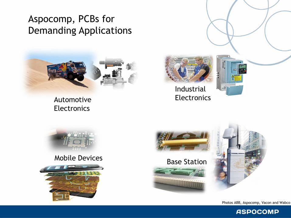
Aspocomp, PCBs for
Demanding Applications
Base Station
Automotive
Electronics
Mobile Devices
Industrial
Electronics
Photos ABB, Aspocomp, Vacon and Wabco
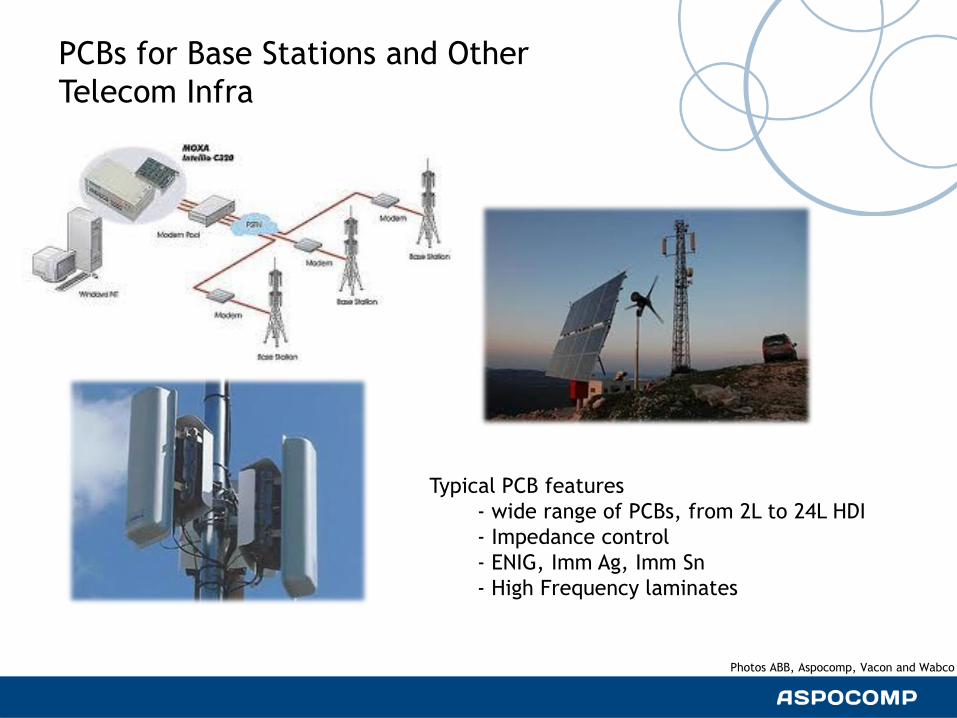
PCBs for Base Stations and Other
Telecom Infra
Photos ABB, Aspocomp, Vacon and Wabco
Typical PCB features
- wide range of PCBs, from 2L to 24L HDI
- Impedance control
- ENIG, Imm Ag, Imm Sn
- High Frequency laminates

PCBs for Automotive Electronics
Photos Wabco, Conti, Aspocomp
Example PCB, HDI 1+2b+1 Alu
metalback
Typical PCB features
- HDI, Multilayer
- High Tg + Mid Tg FR4, ENIG
- Aluminum back
- Automotive quality procedures
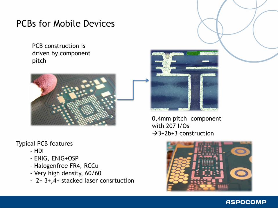
PCBs for Mobile Devices
PCB construction is
driven by component
pitch
0,4mm pitch component
with 207 I/Os
3+2b+3 construction
Typical PCB features
- HDI
- ENIG, ENIG+OSP
- Halogenfree FR4, RCCu
- Very high density, 60/60
- 2+ 3+,4+ stacked laser consrtuction
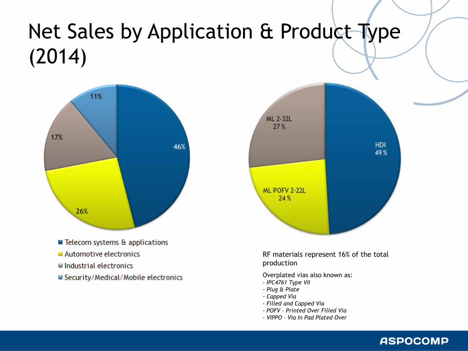
Net Sales by Application & Product Type
(2014)
RF materials represent 16% of the total
production
Overplated vias also known as: - IPC4761 Type VII
- Plug & Plate
- Capped Via
- Filled and Capped Via
- POFV – Printed Over Filled Via
- VIPPO – Via In Pad Plated Over
46%
26%
17%
11%
Telecom systems & applicationsAutomotive electronicsIndustrial electronicsOther electronics

Examples of HDI PCB Construction
1+4b+1 2+4b+2 stacked
3+2b+3 stacked 2+4b+2 staggered
’ stacked’
’ staggered’

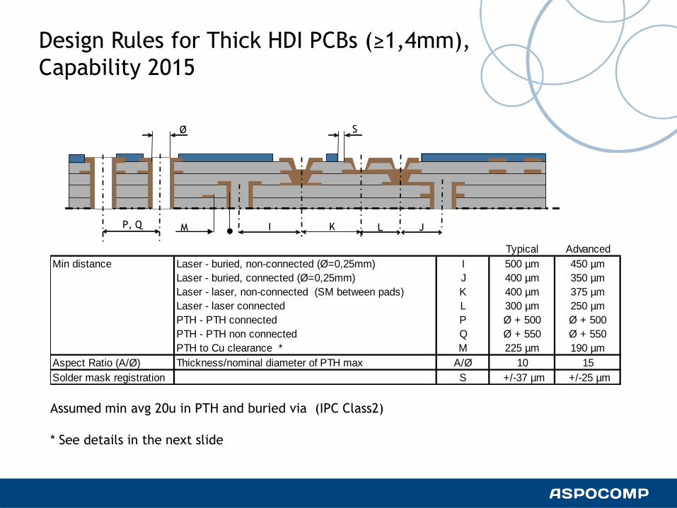
Design Rules for Thick HDI PCBs (≥1,4mm),
Capability 2015
Assumed min avg 20u in PTH and buried via (IPC Class2)
B C D
E
A
F G
T
Ø Ø
Typical Advanced
PWB thickness PCB final A 2,4 mm 5,5mm
Inner layer core 18/18 thickness min T 63µm 50µm
Min conductor width Copper thickness < 25 µm (non-plated I/L) B 75 µm 60 µm
Copper thickness 25u - 50u B 90 µm 75 µm
Min space Copper thickness < 25 µm (non-plated I/L) C 75 µm 60 µm
Copper thickness 25u - 50u C 90 µm 75 µm
Min hole diameter With board thickness 2,4mm Ø 250 µm 200 µm
Min pad size Via hole, outer layer (Ø=0,25mm ) D 550 µm 450 µm
(no break) Via hole, inner layer (Ø=0,25mm) E 550 µm 450 µm
Buried holes (Ø=0,25mm) F 550 µm 450 µm
Laser hole, surface pad G 250 µm 250 µm
Laser hole, inner layer pad, dielectric <=70u H 220 µm 220 µm
Laser hole, inner layer pad, dielectric <=100u H 250 µm 250 µm
S
L K J I M
Ø
P, Q
Assumed min avg 20u in PTH and buried via (IPC Class2)
* See details in the next slide
Design Rules for Thick HDI PCBs (≥1,4mm),
Capability 2015
Typical Advanced
Min distance Laser - buried, non-connected (Ø=0,25mm) I 500 µm 450 µm
Laser - buried, connected (Ø=0,25mm) J 400 µm 350 µm
Laser - laser, non-connected (SM between pads) K 400 µm 375 µm
Laser - laser connected L 300 µm 250 µm
PTH - PTH connected P Ø + 500 Ø + 500
PTH - PTH non connected Q Ø + 550 Ø + 550
PTH to Cu clearance * M 225 µm 190 µm
Aspect Ratio (A/Ø) Thickness/nominal diameter of PTH max A/Ø 10 15
Solder mask registration S +/-37 µm +/-25 µm
12th of Jan 2015 10
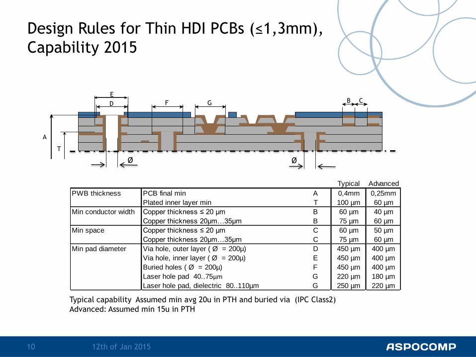
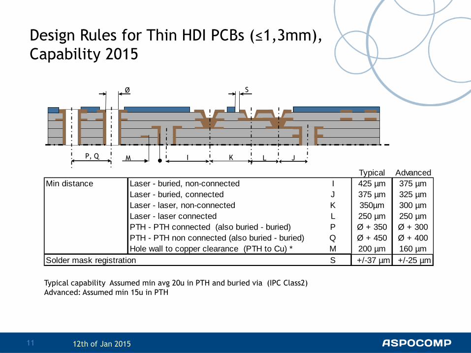
Design Rules for Thin HDI PCBs (≤1,3mm),
Capability 2015
Typical capability Assumed min avg 20u in PTH and buried via (IPC Class2)
Advanced: Assumed min 15u in PTH
B C D
E
A
F G
T
Ø Ø
Typical Advanced
PWB thickness PCB final min A 0,4mm 0,25mm
Plated inner layer min T 100 µm 60 µm
Min conductor width Copper thickness ≤ 20 µm B 60 µm 40 µm
Copper thickness 20µm…35µm B 75 µm 60 µm
Min space Copper thickness ≤ 20 µm C 60 µm 50 µm
Copper thickness 20µm…35µm C 75 µm 60 µm
Min pad diameter Via hole, outer layer ( Ø = 200µ) D 450 µm 400 µm
Via hole, inner layer ( Ø = 200µ) E 450 µm 400 µm
Buried holes ( Ø = 200µ) F 450 µm 400 µm
Laser hole pad 40..75µm G 220 µm 180 µm
Laser hole pad, dielectric 80..110µm G 250 µm 220 µm
11
S
L K J I M
Ø
P, Q
12th of Jan 2015
Typical capability Assumed min avg 20u in PTH and buried via (IPC Class2)
Advanced: Assumed min 15u in PTH
Typical Advanced
Min distance Laser - buried, non-connected I 425 µm 375 µm
Laser - buried, connected J 375 µm 325 µm
Laser - laser, non-connected K 350µm 300 µm
Laser - laser connected L 250 µm 250 µm
PTH - PTH connected (also buried - buried) P Ø + 350 Ø + 300
PTH - PTH non connected (also buried - buried) Q Ø + 450 Ø + 400
Hole wall to copper clearance (PTH to Cu) * M 200 µm 160 µm
Solder mask registration S +/-37 µm +/-25 µm
Design Rules for Thin HDI PCBs (≤1,3mm),
Capability 2015
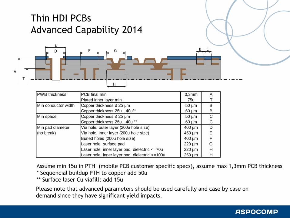
Please note that advanced parameters should be used carefully and case by case on
demand since they have significant yield impacts.
B C D
E
A
F G
H
T
Assume min 15u in PTH (mobile PCB customer specific specs), assume max 1,3mm PCB thickness
* Sequencial buildup PTH to copper add 50u
** Surface laser Cu viafill: add 15u
PWB thickness PCB final min 0,3mm A
Plated inner layer min 75u T
Min conductor width Copper thickness ≤ 25 µm 50 µm B
Copper thickness 25u…40u** 60 µm B
Min space Copper thickness ≤ 25 µm 50 µm C
Copper thickness 25u…40u ** 60 µm C
Min pad diameter Via hole, outer layer (200u hole size) 400 µm D
(no break) Via hole, inner layer (200u hole size) 450 µm E
Buried holes (200u hole size) 400 µm F
Laser hole, surface pad 220 µm G
Laser hole, inner layer pad, dielectric <=70u 220 µm H
Laser hole, inner layer pad, dielectric <=100u 250 µm H
Thin HDI PCBs
Advanced Capability 2014

PTH wall (by
nominal
diameter)
Risk of short circuit if
too low PTH to Cu
PTH to Cu
Clearance Requirement at Inner Layers
Clearance
PTH to Cu
Clearance
PTH to Cu
Area of the annular ring is
required for true drill
position tolerance
(regardless if there is
annular ring or not)
PTH to Cu Drill length L
Required safe PTH to Cu parameter is depending
on the length and the diameter of the associated
drilling :
L max Ø0,2 Ø0,3 ≥Ø0,35
1,6µm 210µm 200µm 190µm
3,2mm N/A 225µm 200µm
For sequential blind please add + 50µm
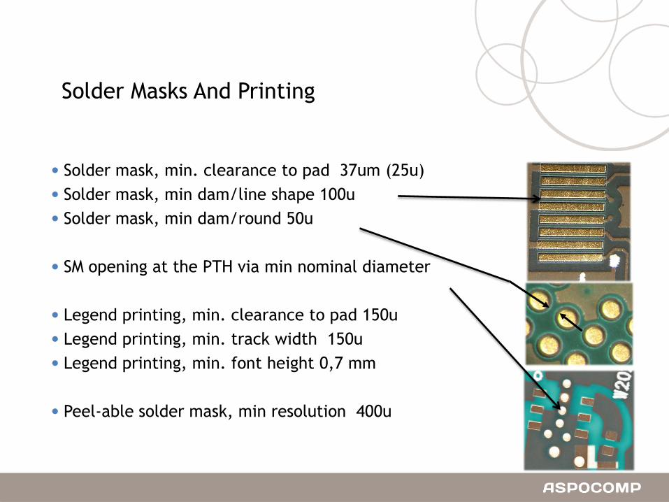
Solder Masks And Printing
• Solder mask, min. clearance to pad 37um (25u)
• Solder mask, min dam/line shape 100u
• Solder mask, min dam/round 50u
• SM opening at the PTH via min nominal diameter
• Legend printing, min. clearance to pad 150u
• Legend printing, min. track width 150u
• Legend printing, min. font height 0,7 mm
• Peel-able solder mask, min resolution 400u
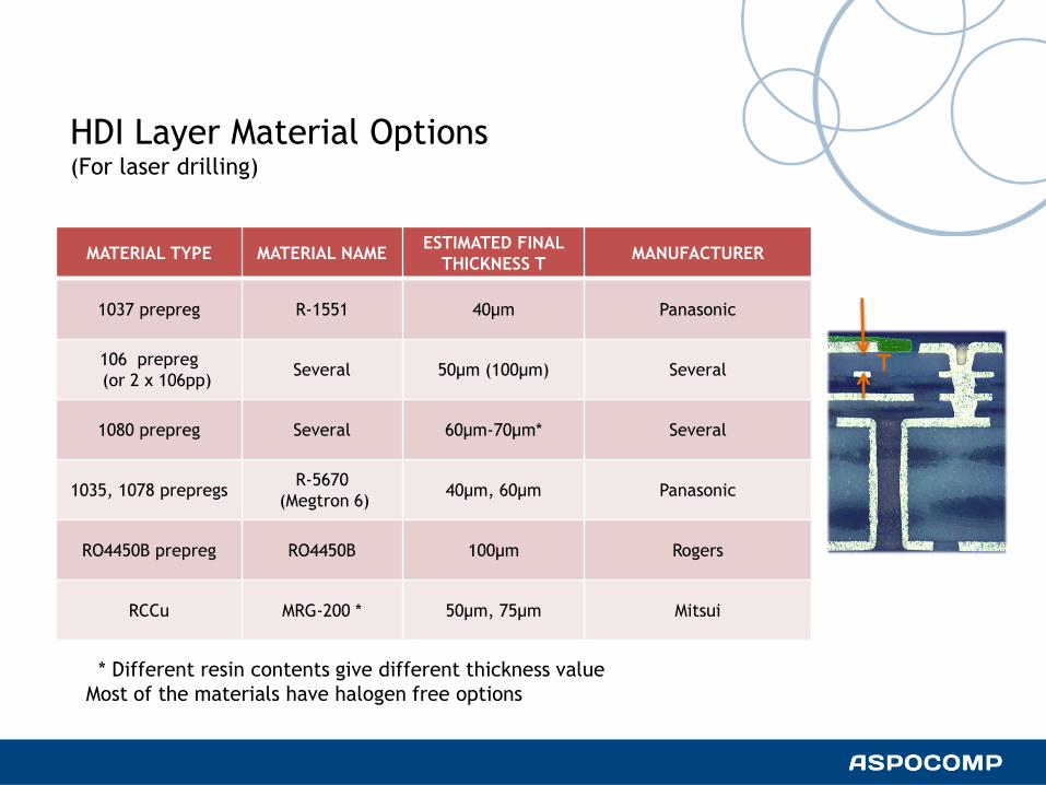
HDI Layer Material Options (For laser drilling)
MATERIAL TYPE MATERIAL NAME ESTIMATED FINAL
THICKNESS T MANUFACTURER
1037 prepreg R-1551 40µm Panasonic
106 prepreg
(or 2 x 10⁶pp) Several 50µm (100µm) Several
1080 prepreg Several 60µm-70µm* Several
1035, 1078 prepregs R-5670
(Megtron 6) 40µm, 60µm Panasonic
RO4450B prepreg RO4450B 100µm Rogers
RCCu MRG-200 * 50µm, 75µm Mitsui
* Different resin contents give different thickness value
Most of the materials have halogen free options
T

Surface Finish Options
ENIG Atotech Aurotech
CNN (mid P)
ENIG /OSP (SIT)
OSP Entek Plus Cu-
106 A (X) HT
HASL SN100C
HASL SnPb
Immersion tin
Atotech Stannatech
Immersion silver
McDermid Sterling
Silver 2.0
Galvanic NiAu
contact surfaces
Additional options available subcontracted

End of the Slides