hdl programing and eda tools … programing and eda tools laboratory manual for i / ii m.tech vlsi...
TRANSCRIPT

, Sir C.R. Reddy College of Engg. Eluru – 7 Dept. of ECE
I/II (M.TECH VLSI DESIGN) ECE, I-SEM :: HDL Programming and EDA Tools Lab Lab Manual
HDL PROGRAMING AND EDA TOOLS LABORATORY
MANUAL
FOR I / II M.TECH VLSI DESIGN (ECE)
I - SEMESTER
DEPT. OF ELECTRONICS AND COMMUNICATION ENGINEERING
SIR C.R.REDDY COLLEGE OF ENGINEERING
ELURU – 534 007
, Sir C.R. Reddy College of Engg. Eluru – 7 Dept. of ECE
I/II (M.TECH VLSI DESIGN) ECE, I-SEM :: HDL Programming and EDA Tools Lab Lab Manual
HDL PROGRAMING AND EDA TOOLS LABORATORY
MANUAL
FOR I / II M.TECH VLSI DESIGN (ECE)
I - SEMESTER LIST OF EXPERIMENTS
INTRODUCTION TO VHDL
1. PROGRAM -1
2. PROGRAM -2
3. PROGRAM -3
4. PROGRAM -4
5. PROGRAM -5
6. PROGRAM -6
7. PROGRAM -7
8. PROGRAM -8
9. PROGRAM -9
10. PROGRAM -10
11. PROGRAM -11
12. PROGRAM -12
13. PROGRAM -13
14. PROGRAM -14
15. PROGRAM -15
16. PROGRAM -16
17. VHDL VIVA QUESTIONS

, Sir C.R. Reddy College of Engg. Eluru – 7 Dept. of ECE
I/II (M.TECH VLSI DESIGN) ECE, I-SEM :: HDL Programming and EDA Tools Lab Lab Manual
INDEX
S.No
Date
Name of the Experiment
Page No
Remarks
1.
LOGIC GATES
2.
FULL ADDER
3.
PARALLEL ADDER , SERIAL ADDER
4.
COMPARATORS 2 BIT,4BIT
5.
MULTIPLEXER & DEMULTIPLEXER
6.
ENCODER, PRORITY ENCODERS
7.
DECODERS
8.
FLIP FLOPS SR,JK,D& T
9.
SHIFT REGISTER
10.
SEQUENCE DETECTOR
11 IMPLEMENTATION OF MEMORY
12 COUNTERS
13 BARELL SHIFTER

, Sir C.R. Reddy College of Engg. Eluru – 7 Dept. of ECE
I/II (M.TECH VLSI DESIGN) ECE, I-SEM :: HDL Programming and EDA Tools Lab Lab Manual
INTRODUCTION TO VHDL
VHDL is an acronym for VHSIC Hardware Description Language (VHSIC is
an acronym for Very High Speed Integrated Circuit).It is a Hardware Description
Language that can be used to model a digital system at many levels of abstraction
,ranging from algorithmic level to the gate level. The complexity of the digital
system being modeled could vary from that of simple gate to a complex digital
electronic system or anything in between. The digital system can also be described
hierarchically. Timing can also be explicitly modeled in the same description.
The VHDL language can be regarded as an integrated amalgamation of
following languages.
Sequential language +
Concurrent language +
Net-list language +
Timing specifications +
Waveform generation language =>VHDL.
The language not only defines the syntax but also defines very clear
simulation semantics for each language construct. Therefore models written in this
language can be verified using a VHDL simulation.
CAPABILITIES:
The following are the major capabilities that the language provides along
with the features that differentiate it from other hardware description languages.
• The language can be used as an exchange medium between chip vendors and
CAD tool users. Different chip vendors can provide VHDL descriptions of their
components to system designers. CAD tool users can use it to capture the
behavior of the design at a high level of abstraction of functional simulation.

, Sir C.R. Reddy College of Engg. Eluru – 7 Dept. of ECE
I/II (M.TECH VLSI DESIGN) ECE, I-SEM :: HDL Programming and EDA Tools Lab Lab Manual
• The language can also be used as a communication medium between different
CAD and CAE tools. For example, a schematic capture program may be used to
generate a VHDL description for the design which can be used as an input to a
simulation program.
• The language supports hierarchy, that is, a digital system can be modeled as a set
of interconnected subcomponents.
• The language supports flexible design methodologies: top-down, bottom-up or
mixed.
• It supports both synchronous and asynchronous timing models.
• Various digital modeling techniques, such as finite state machine descriptions,
algorithmic descriptions and Boolean equations can be modeled using the
language.
• The language supports three basic different description styles: structural, dataflow
and behavioral. A design may also be expressed in any combination of these three
descriptive styles.
• The language is not technology-specific, but is capable of supporting technology
specific features. It can also support various hardware technologies.
BASIC TERMINOLOGY:
A hardware abstraction of a digital system is called an entity. An entity X
when used in another entity Y becomes a component for the entity Y. therefore the
component is also an entity, depending on the level at which you are trying to model.
To describe an entity, VHDL provides five different types of primary
constructs called design units. They are:
� Entity declaration.
� Architecture body.
� Configuration declaration.

, Sir C.R. Reddy College of Engg. Eluru – 7 Dept. of ECE
I/II (M.TECH VLSI DESIGN) ECE, I-SEM :: HDL Programming and EDA Tools Lab Lab Manual
� Package declaration.
� Package body.
• ENTITY DECLARATION:
The entity declaration specifies the name of the entity being modeled and lists
the set of interface ports. Ports are signals through which the entity communicates
with the other models in its external environment.
• ARCHITECTURE BODY:
The internal details of an entity are specified by an architecture body using
any of the following modeling styles:
� As a set of interconnected components (to represent structure).
� As a set of concurrent assignment statements (to represent dataflow).
� As a set of sequential assignment statements (to represent behavior).
• CONFIGURATION DECLARATION:
This is used to select one of the many possibly architecture bodies that an
entity may have, and to bind components , used to represent structure in that
architecture body, to entities represented by an entity-architecture pair or by a
configuration which reside in a design library.
• PACKAGE DECLARATION:
This is used to store a set of common declarations, such as components, types,
procedures and functions. These declarations can then be imported into other design
units using a ‘use’ clause.

, Sir C.R. Reddy College of Engg. Eluru – 7 Dept. of ECE
I/II (M.TECH VLSI DESIGN) ECE, I-SEM :: HDL Programming and EDA Tools Lab Lab Manual
• PACKAGE BODY:
This is used to store the definitions of functions and procedures that were
declared in the corresponding package declaration, and also complete constant
declarations for any deferred constants that appear in the package in the package
declaration.
STRUCTURAL MODELING:
In the structural style of modeling, an entity is described as a set of
interconnected components. Example: Half adder. The entity declaration for half
adder specifies the interface ports for this architecture body. The architecture body is
composed of two parts: the declarative part (before the keyword begin) and the
statement part(after the keyword begin). Two component declarations are present in
the declarative part of the architecture body. These declarations specify the interface
of components that are used in the architecture body. The declared components are
instantiated in the statement part of the architecture body using component labels for
these component instantiation statements. The signals in the port map of a
component instantiated and the port signals in the component declaration are
associated by position (called positional association). However the structural
representation for the Half adder does not say anything about its functionality.
Separate entity models would be described for the components XOR2 and AND2,
each having its own entity declaration and architecture body.
A component instantiated statement is a concurrent statement. Therefore, the
order of these statements is not important. The structural style of modeling describes

, Sir C.R. Reddy College of Engg. Eluru – 7 Dept. of ECE
I/II (M.TECH VLSI DESIGN) ECE, I-SEM :: HDL Programming and EDA Tools Lab Lab Manual
only an interconnection of components, without implying any behavior of the
components themselves nor the entity that they collectively represent.
DATAFLOW MODELING:
In this modeling style, the flow of data through the entity is expressed
primarily using concurrent signal assignment statements. The structure entity of the
entity is not explicitly specified in this modeling style, but it can be implicitly
deduced. In a signal assignment statement, the symbol <= implies an assignment of a
value to a signal. The value of the expression on the right-hand-side of the statement
is computed and is assigned to the signal on the left-hand-side, called the target
signal. A concurrent signal assignment statement is executed only when any signal
used in the expression on the right-hand-side has an event on it, that is, the value for
the signal changes.
BEHAVIORAL MODELING:
The behavioral modeling specifies the behavior of an entity as a set of
statements that are executed sequentially in the specified order. This set of sequential
statements, which are specified inside a process statement, do not explicitly specify
the structure of the entity but merely its functionality. A process statement is a
concurrent statement that can appear within an architecture body. A process
statement also has a declarative part (before the keyword begin) and a statement part
(between the keywords begin and end process). The statements appearing within the
statement part are sequential statements and are executed sequentially. The list of
signals specified within the parenthesis after the keyword process constitutes a
sensitivity list, and the process statement is invoked whenever there is an event on
any signal in this list.
A variable is assigned using the assignment operator := compound symbol;
contrast this with a signal that is assigned a value using the assignment operator <=
compound symbol. Signal assignment statements appearing within a process are
, Sir C.R. Reddy College of Engg. Eluru – 7 Dept. of ECE
I/II (M.TECH VLSI DESIGN) ECE, I-SEM :: HDL Programming and EDA Tools Lab Lab Manual
called sequential signal assignment statements. Sequential signal statements,
including variable assignment statements, are executed sequentially independent of
whether an event occurs on any signals in its right-hand-side expression; contrast
this with the execution of concurrent signal assignment statements in the dataflow
modeling style.
PROGRAM -1

, Sir C.R. Reddy College of Engg. Eluru – 7 Dept. of ECE
I/II (M.TECH VLSI DESIGN) ECE, I-SEM :: HDL Programming and EDA Tools Lab Lab Manual
PROGRAM -1
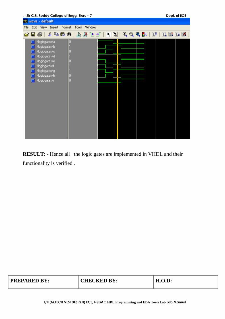
AIM: - To write a program in VHDL for implementing the basic gates-
AND, OR, OT, NAND, NOR, XOR, XNOR and to verify the functionality.
PROGRAM :- library ieee;
use ieee.std_logic_1164.all;
entity logicgates is
port(a,b: in std_logic;c,d,e,f,g,h,i: out std_logic);
end logicgates;
architecture dataflow of logicgates is
begin
c<= a and b;
d<= a or b;
e<= not b;
f<= a xor b;
g<= a nand b;
h<= not(a xor b);
i<= a nor b;
end dataflow;
TRUTH TABLE :-

, Sir C.R. Reddy College of Engg. Eluru – 7 Dept. of ECE
I/II (M.TECH VLSI DESIGN) ECE, I-SEM :: HDL Programming and EDA Tools Lab Lab Manual
RTL SCHEMATIC:
INPUTS OUTPUTS
a b c d e f g h i
0 0 0 0 1 0 1 1 1
0 1 0 1 0 1 1 0 0
1 0 0 1 1 1 1 0 0
1 1 1 1 0 0 0 1 0

, Sir C.R. Reddy College of Engg. Eluru – 7 Dept. of ECE
I/II (M.TECH VLSI DESIGN) ECE, I-SEM :: HDL Programming and EDA Tools Lab Lab Manual
WAVEFORMS:
BASIC LOGIC GATES
, Sir C.R. Reddy College of Engg. Eluru – 7 Dept. of ECE
I/II (M.TECH VLSI DESIGN) ECE, I-SEM :: HDL Programming and EDA Tools Lab Lab Manual
RESULT: - Hence all the logic gates are implemented in VHDL and their
functionality is verified .
PREPARED BY: CHECKED BY: H.O.D:
, Sir C.R. Reddy College of Engg. Eluru – 7 Dept. of ECE
I/II (M.TECH VLSI DESIGN) ECE, I-SEM :: HDL Programming and EDA Tools Lab Lab Manual
PROGRAM-2
, Sir C.R. Reddy College of Engg. Eluru – 7 Dept. of ECE
I/II (M.TECH VLSI DESIGN) ECE, I-SEM :: HDL Programming and EDA Tools Lab Lab Manual
PROGRAM 2(a)
AIM: - To write a program in VHDL for implementing the half adder and to verify
the functionality.
PROGRAM :-
library ieee;
use ieee.std_logic_1164.all;
entity halfadder is
port(a,b: in std_logic;s,c: out std_logic);
end halfadder;
architecture dataflow of halfadder is
begin
s<= a xor b;
c<= a and b;
end dataflow;
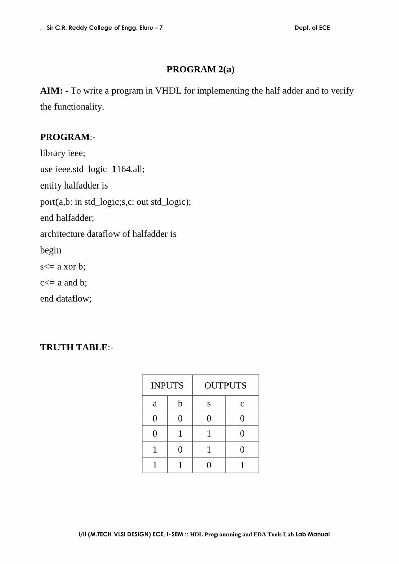
TRUTH TABLE :-
INPUTS OUTPUTS
a b s c
0 0 0 0
0 1 1 0
1 0 1 0
1 1 0 1

, Sir C.R. Reddy College of Engg. Eluru – 7 Dept. of ECE
I/II (M.TECH VLSI DESIGN) ECE, I-SEM :: HDL Programming and EDA Tools Lab Lab Manual
RTL SCHEMATIC:
WAVEFORMS:
RESULT:- Hence the halfadder is implemented in VHDL and the functionality is
verified .
PREPARED BY: CHECKED BY: H.O.D:
HALF ADDER

, Sir C.R. Reddy College of Engg. Eluru – 7 Dept. of ECE
I/II (M.TECH VLSI DESIGN) ECE, I-SEM :: HDL Programming and EDA Tools Lab Lab Manual
PROGRAM 2(b)
AIM: - To write a program in VHDL for implementing the full adder and to verify
the functionality.
PROGRAM :-
library ieee;
use ieee.std_logic_1164.all;
entity fulladder is
port(a,b,c: in std_logic;s,cy: out std_logic);
end fulladder;
architecture dataflow of fulladder is
begin
s<= (a xor b)xor c;
cy<= (a and b) or (b and c) or (c and a);
end dataflow;
TRUTH TABLE :-
INPUTS OUTPUTS
a b c s cy 0 0 0 0 0 0 0 1 1 0 0 1 0 1 0 0 1 1 0 1 1 0 0 1 0 1 0 1 0 1 1 1 0 0 1 1 1 1 1 1
, Sir C.R. Reddy College of Engg. Eluru – 7 Dept. of ECE
I/II (M.TECH VLSI DESIGN) ECE, I-SEM :: HDL Programming and EDA Tools Lab Lab Manual
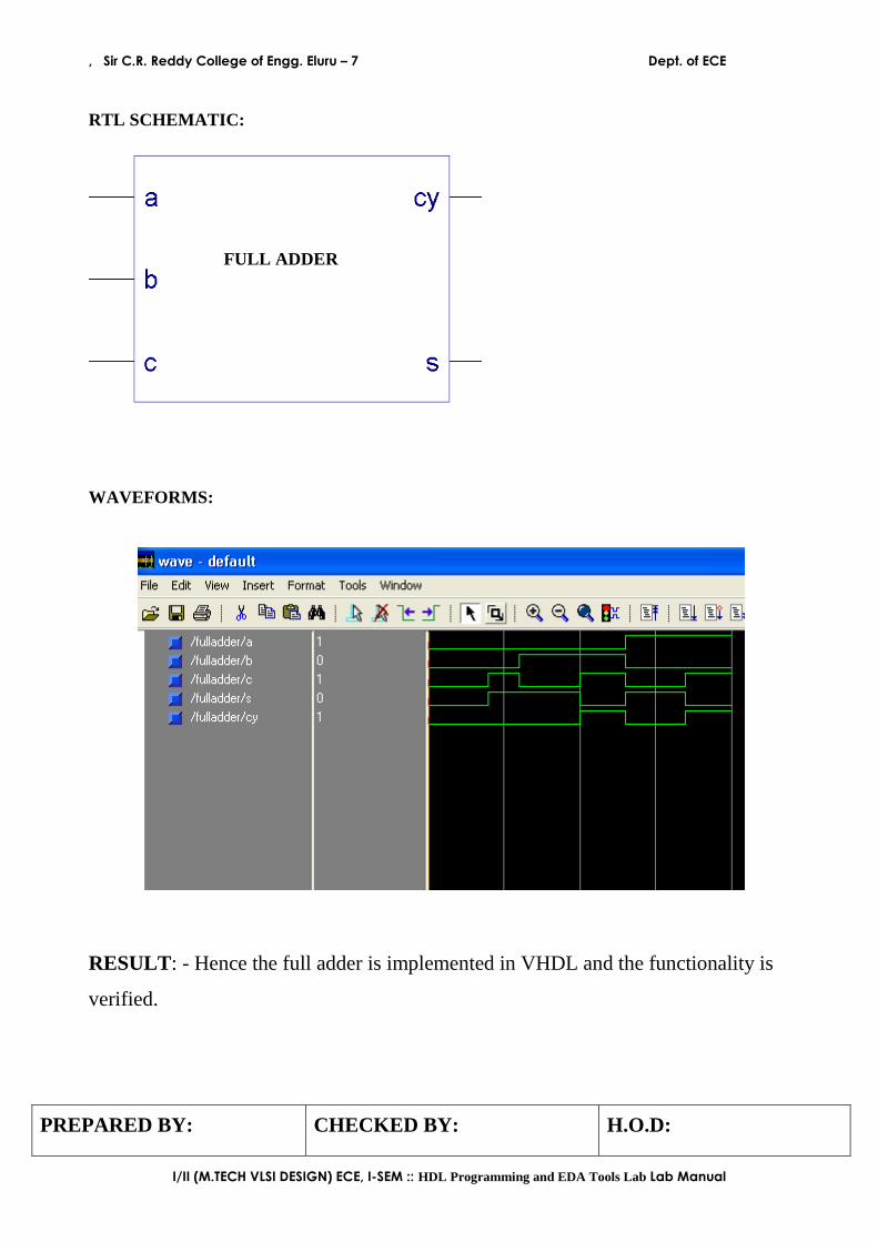
RTL SCHEMATIC:
WAVEFORMS:
RESULT: - Hence the full adder is implemented in VHDL and the functionality is
verified.
PREPARED BY: CHECKED BY: H.O.D:
FULL ADDER

, Sir C.R. Reddy College of Engg. Eluru – 7 Dept. of ECE
I/II (M.TECH VLSI DESIGN) ECE, I-SEM :: HDL Programming and EDA Tools Lab Lab Manual
PROGRAM-3
, Sir C.R. Reddy College of Engg. Eluru – 7 Dept. of ECE
I/II (M.TECH VLSI DESIGN) ECE, I-SEM :: HDL Programming and EDA Tools Lab Lab Manual
PROGRAM 3(a)
AIM: - To write a program in VHDL for implementing the half subtractor and to
verify the functionality.
PROGRAM :-
library ieee;
use ieee.std_logic_1164.all;
entity halfsub is
port(a,b: in std_logic;d,br: out std_logic);
end halfsub;
architecture dataflow of halfsub is
begin
d<= a xor b;
br<= (not a) and b;
end dataflow;
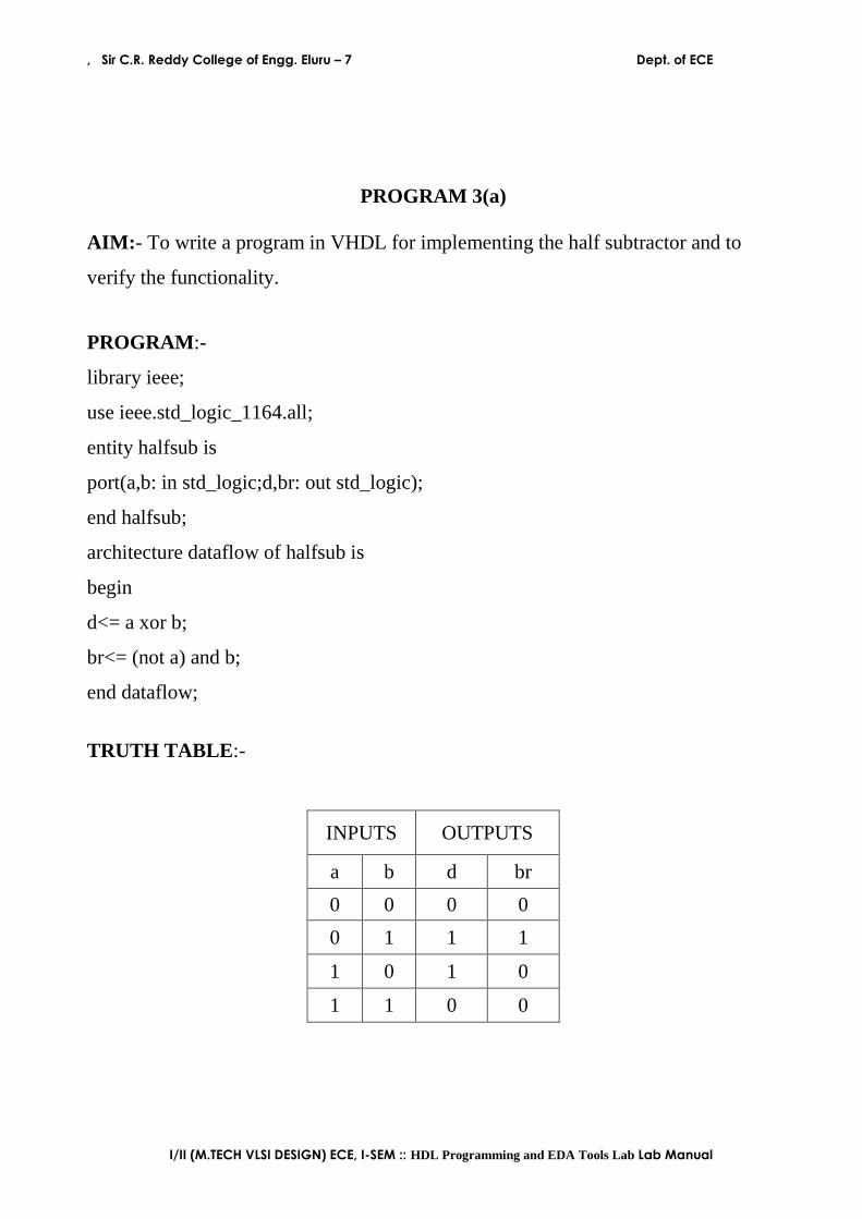
TRUTH TABLE :-
INPUTS OUTPUTS
a b d br
0 0 0 0
0 1 1 1
1 0 1 0
1 1 0 0
, Sir C.R. Reddy College of Engg. Eluru – 7 Dept. of ECE
I/II (M.TECH VLSI DESIGN) ECE, I-SEM :: HDL Programming and EDA Tools Lab Lab Manual
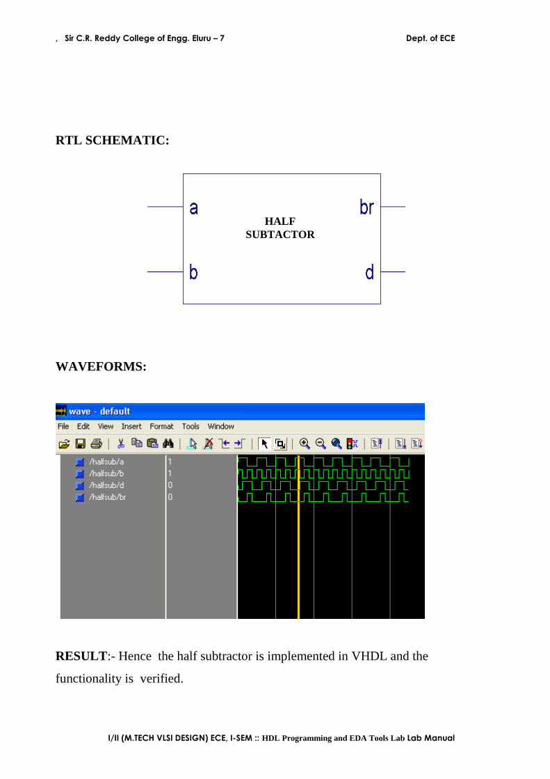
RTL SCHEMATIC:
WAVEFORMS:
RESULT:- Hence the half subtractor is implemented in VHDL and the
functionality is verified.
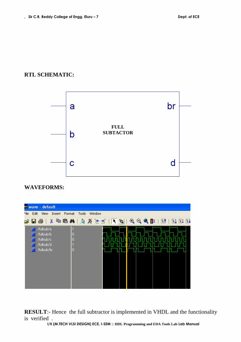
HALF SUBTACTOR

, Sir C.R. Reddy College of Engg. Eluru – 7 Dept. of ECE
I/II (M.TECH VLSI DESIGN) ECE, I-SEM :: HDL Programming and EDA Tools Lab Lab Manual
PROGRAM 3(b)
AIM: - To write a program in VHDL for implementing the full subtractor and to
verify the functionality.
PROGRAM :-
library ieee;
use ieee.std_logic_1164.all;
entity fullsub is
port(a,b,c: in std_logic;d,br: out std_logic);
end fullsub;
architecture dataflow of fullsub is
begin
d<= (a xor b)xor c;
br<= ((not a) and b) or ((not a) and c) or (b and c);
end dataflow;
TRUTH TABLE :-
INPUTS OUTPUTS
a b c d br 0 0 0 0 0 0 0 1 1 1 0 1 0 1 1 0 1 1 0 0 1 0 0 1 0 1 0 1 0 0 1 1 0 0 0 1 1 1 1 1
PREPARED BY: CHECKED BY: H.O.D:
, Sir C.R. Reddy College of Engg. Eluru – 7 Dept. of ECE
I/II (M.TECH VLSI DESIGN) ECE, I-SEM :: HDL Programming and EDA Tools Lab Lab Manual
RTL SCHEMATIC:
WAVEFORMS:
RESULT:- Hence the full subtractor is implemented in VHDL and the functionality is verified .
FULL SUBTACTOR
, Sir C.R. Reddy College of Engg. Eluru – 7 Dept. of ECE
I/II (M.TECH VLSI DESIGN) ECE, I-SEM :: HDL Programming and EDA Tools Lab Lab Manual
PROGRAM -4
PREPARED BY: CHECKED BY: H.O.D:

, Sir C.R. Reddy College of Engg. Eluru – 7 Dept. of ECE
I/II (M.TECH VLSI DESIGN) ECE, I-SEM :: HDL Programming and EDA Tools Lab Lab Manual
PROGRAM 4
AIM: - To write a program in VHDL for implementing the full adder using two half
adders and to verify the functionality.
PROGRAM :-
COMPONENT OR2:-
library ieee;
use ieee.std_logic_1164.all;
entity or2 is
port(a,b: in std_logic;c: out std_logic);
end or2;
architecture dataflow of or2 is
begin
c<= a or b;
end dataflow;
TOP MODULE:-
library ieee;
use ieee.std_logic_1164.all;
entity fa_ha is
port(a,b,c: in std_logic;s,cy: out std_logic);
end fa_ha;
architecture structure of fa_ha is
component halfadder

, Sir C.R. Reddy College of Engg. Eluru – 7 Dept. of ECE
I/II (M.TECH VLSI DESIGN) ECE, I-SEM :: HDL Programming and EDA Tools Lab Lab Manual
port(a,b: in std_logic;s,c: out std_logic);
end component;
component or2
port(a,b: in std_logic;c: out std_logic);
end component;
signal s1,t1,t2: std_logic;
begin
x1: halfadder port map(a,b,s1,t1);
x2: halfadder port map(s1,c,s,t2);
x3: or2 port map(t1,t2,cy);
end structure;
TRUTH TABLE :-
INPUTS OUTPUTS
a b c s cy 0 0 0 0 0 0 0 1 1 0 0 1 0 1 0 0 1 1 0 1 1 0 0 1 0 1 0 1 0 1 1 1 0 0 1 1 1 1 1 1
RTL SCHEMATIC:

, Sir C.R. Reddy College of Engg. Eluru – 7 Dept. of ECE
I/II (M.TECH VLSI DESIGN) ECE, I-SEM :: HDL Programming and EDA Tools Lab Lab Manual
WAVEFORMS:
RESULT:- Hence the full adder using two half adders is implemented in VHDL
and the functionality is verified.
HA1 OR2
HA2

, Sir C.R. Reddy College of Engg. Eluru – 7 Dept. of ECE
I/II (M.TECH VLSI DESIGN) ECE, I-SEM :: HDL Programming and EDA Tools Lab Lab Manual
PREPARED BY: CHECKED BY: H.O.D:

, Sir C.R. Reddy College of Engg. Eluru – 7 Dept. of ECE
I/II (M.TECH VLSI DESIGN) ECE, I-SEM :: HDL Programming and EDA Tools Lab Lab Manual
PROGRAM-5
PROGRAM 5(a)
AIM: - To write a program in VHDL for implementing the 2 to 4 decoder and to
verify the functionality.
PROGRAM :-
COMPONENT NAND3:-
library ieee;
use ieee.std_logic_1164.all;
entity nand3 is
port(a,b,c: in std_logic;d: out std_logic);
end nand3;
architecture dataflow of nand3 is

, Sir C.R. Reddy College of Engg. Eluru – 7 Dept. of ECE
I/II (M.TECH VLSI DESIGN) ECE, I-SEM :: HDL Programming and EDA Tools Lab Lab Manual
begin
d<= (a nand b) nand c;
end dataflow;
COMPONENT INV2:-
library ieee;
use ieee.std_logic_1164.all;
entity inv2 is
port(a: in std_logic;b: out std_logic);
end inv2;
architecture dataflow of inv2 is
begin
b<= not(a);
end dataflow;
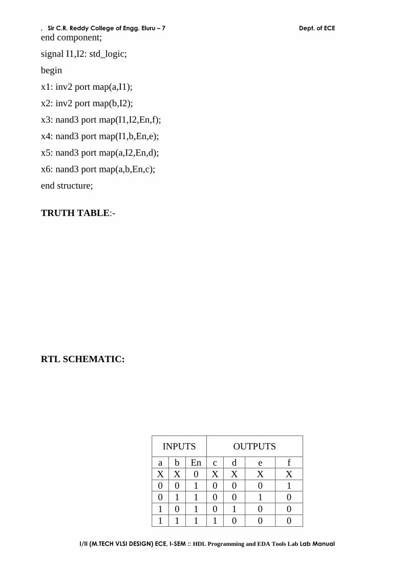
TOP MODULE:-
library ieee;
use ieee.std_logic_1164.all;
entity d24 is
port(a,b,En: in std_logic;f,e,d,c: out std_logic);
end d24;
architecture structure of d24 is
component nand3
port(a,b,c: in std_logic;d: out std_logic);
end component;
component inv2
port(a: in std_logic;b: out std_logic);
, Sir C.R. Reddy College of Engg. Eluru – 7 Dept. of ECE
I/II (M.TECH VLSI DESIGN) ECE, I-SEM :: HDL Programming and EDA Tools Lab Lab Manual
end component;
signal I1,I2: std_logic;
begin
x1: inv2 port map(a,I1);
x2: inv2 port map(b,I2);
x3: nand3 port map(I1,I2,En,f);
x4: nand3 port map(I1,b,En,e);
x5: nand3 port map(a,I2,En,d);
x6: nand3 port map(a,b,En,c);
end structure;
TRUTH TABLE :-
RTL SCHEMATIC:
INPUTS OUTPUTS
a b En c d e f X X 0 X X X X 0 0 1 0 0 0 1 0 1 1 0 0 1 0 1 0 1 0 1 0 0 1 1 1 1 0 0 0

, Sir C.R. Reddy College of Engg. Eluru – 7 Dept. of ECE
I/II (M.TECH VLSI DESIGN) ECE, I-SEM :: HDL Programming and EDA Tools Lab Lab Manual
WAVEFORMS:
INV1
INV1
NAND3
NAND3
NAND3
NAND3
, Sir C.R. Reddy College of Engg. Eluru – 7 Dept. of ECE
I/II (M.TECH VLSI DESIGN) ECE, I-SEM :: HDL Programming and EDA Tools Lab Lab Manual
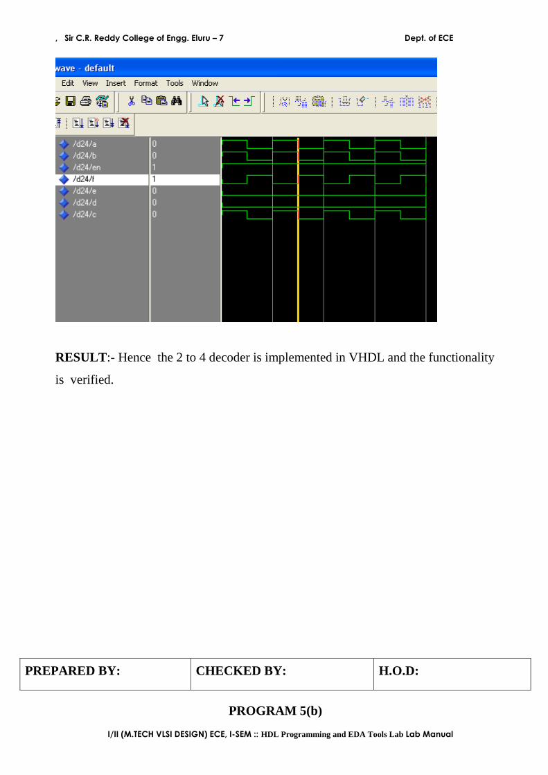
RESULT:- Hence the 2 to 4 decoder is implemented in VHDL and the functionality
is verified.
PROGRAM 5(b)
PREPARED BY: CHECKED BY: H.O.D:

, Sir C.R. Reddy College of Engg. Eluru – 7 Dept. of ECE
I/II (M.TECH VLSI DESIGN) ECE, I-SEM :: HDL Programming and EDA Tools Lab Lab Manual
AIM: - To write a code in VHDL for implementing the 3 to 8 decoder and to verify
the functionality.
PROGRAM :-
library ieee;
use ieee.std_logic_1164.all;
entity d38 is
port(p: in std_logic_vector(2 downto 0);e: in std_logic;y: out std_logic_vector(7
downto 0));
end d38;
architecture beh of d38 is
begin
process(e,p)
begin
if(e='1') then
case p is
when "000"=>y<="00000001";
when "001"=>y<="00000010";
when "010"=>y<="00000100";
when "011"=>y<="00001000";
when "100"=>y<="00010000";
when "101"=>y<="00100000";
when "110"=>y<="01000000";
when "111"=>y<="10000000";
when others=>y<="00000000";
end case;
else
y<="11111111";
end if;
end process;
end beh;
, Sir C.R. Reddy College of Engg. Eluru – 7 Dept. of ECE
I/II (M.TECH VLSI DESIGN) ECE, I-SEM :: HDL Programming and EDA Tools Lab Lab Manual
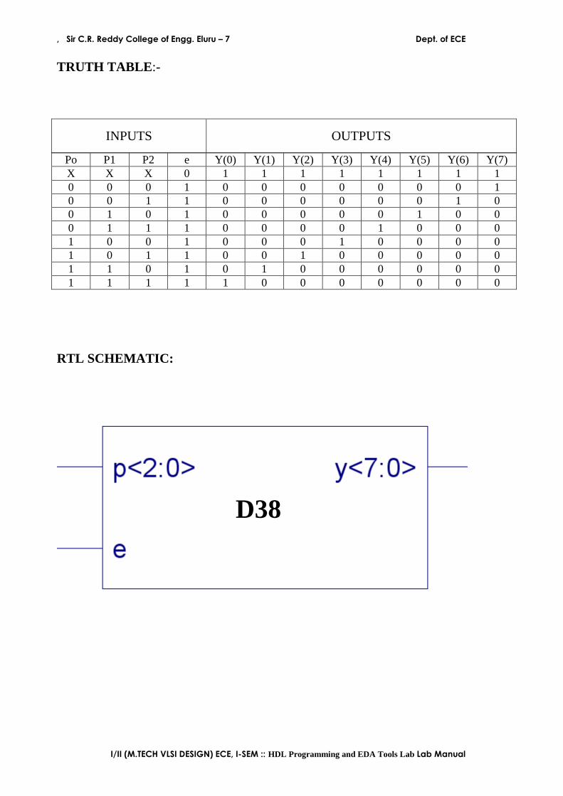
TRUTH TABLE :-
RTL SCHEMATIC:
Po P1 P2 e Y(0) Y(1) Y(2) Y(3) Y(4) Y(5) Y(6) Y(7) X X X 0 1 1 1 1 1 1 1 1 0 0 0 1 0 0 0 0 0 0 0 1 0 0 1 1 0 0 0 0 0 0 1 0 0 1 0 1 0 0 0 0 0 1 0 0 0 1 1 1 0 0 0 0 1 0 0 0 1 0 0 1 0 0 0 1 0 0 0 0 1 0 1 1 0 0 1 0 0 0 0 0 1 1 0 1 0 1 0 0 0 0 0 0 1 1 1 1 1 0 0 0 0 0 0 0
INPUTS OUTPUTS
D38

, Sir C.R. Reddy College of Engg. Eluru – 7 Dept. of ECE
I/II (M.TECH VLSI DESIGN) ECE, I-SEM :: HDL Programming and EDA Tools Lab Lab Manual
WAVEFORMS:
RESULT:- Hence the 3 to 8 decoder is implemented in VHDL and the functionality
is verified.
PREPARED BY: CHECKED BY: H.O.D:

, Sir C.R. Reddy College of Engg. Eluru – 7 Dept. of ECE
I/II (M.TECH VLSI DESIGN) ECE, I-SEM :: HDL Programming and EDA Tools Lab Lab Manual
PROGRAM-6

, Sir C.R. Reddy College of Engg. Eluru – 7 Dept. of ECE
I/II (M.TECH VLSI DESIGN) ECE, I-SEM :: HDL Programming and EDA Tools Lab Lab Manual
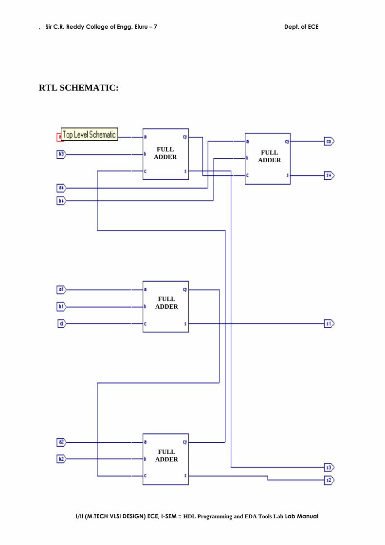
PROGRAM-6
AIM: - To write a code in VHDL for implementing the 4 bit binary adder and to
verify the functionality.
PROGRAM :-
library ieee;
use ieee.std_logic_1164.all;
entity ba_fa is
port(a1,b1,a2,b2,a3,b3,a4,b4,ci: in std_logic;s1,s2,s3,s4,co: out std_logic);
end ba_fa;
architecture structure of ba_fa is
component fulladder
port(a,b,c: in std_logic;s,cy: out std_logic);
end component;
signal c1,c2,c3: std_logic;
begin
X1: fulladder port map(a1,b1,ci,s1,c1);
X2: fulladder port map(a2,b2,c1,s2,c2);
X3: fulladder port map(a3,b3,c2,s3,c3);
X4: fulladder port map(a4,b4,c3,s4,co);
end structure;
, Sir C.R. Reddy College of Engg. Eluru – 7 Dept. of ECE
I/II (M.TECH VLSI DESIGN) ECE, I-SEM :: HDL Programming and EDA Tools Lab Lab Manual
RTL SCHEMATIC:
FULL ADDER
FULL ADDER
FULL ADDER
FULL ADDER
, Sir C.R. Reddy College of Engg. Eluru – 7 Dept. of ECE
I/II (M.TECH VLSI DESIGN) ECE, I-SEM :: HDL Programming and EDA Tools Lab Lab Manual
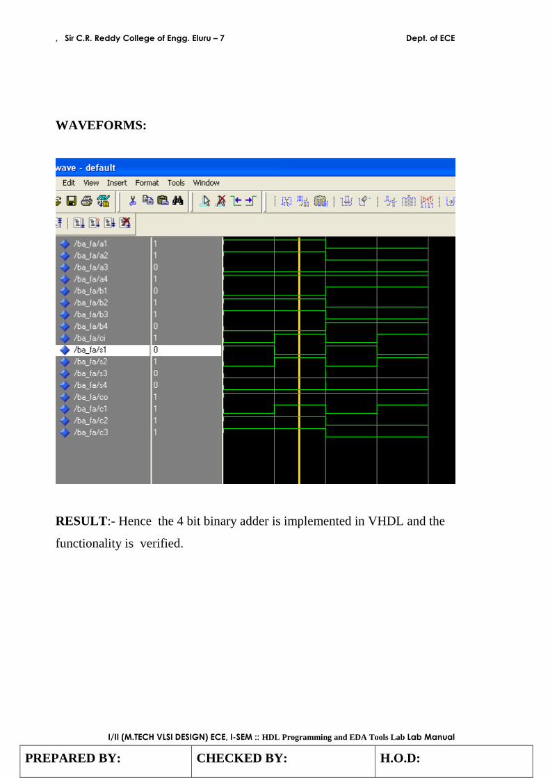
WAVEFORMS:
RESULT:- Hence the 4 bit binary adder is implemented in VHDL and the
functionality is verified.
PREPARED BY: CHECKED BY: H.O.D:

, Sir C.R. Reddy College of Engg. Eluru – 7 Dept. of ECE
I/II (M.TECH VLSI DESIGN) ECE, I-SEM :: HDL Programming and EDA Tools Lab Lab Manual
PROGRAM-7

, Sir C.R. Reddy College of Engg. Eluru – 7 Dept. of ECE
I/II (M.TECH VLSI DESIGN) ECE, I-SEM :: HDL Programming and EDA Tools Lab Lab Manual
PROGRAM 7(a)
AIM: - To write a code in VHDL for implementing the 2x1 multiplexer and to verify
the functionality.
PROGRAM :-
library ieee;
use ieee.std_logic_1164.all;
entity mux21 is
port(a,b:in std_logic;s:in std_logic;y:out std_logic);
end mux21;
architecture beh of mux21 is
begin
process(a,b,s)
begin
case s is
when '0'=>y<=a;
when '1'=>y<=b;
when others=>y<='U';
end case;
end process;
end beh;
TRUTH TABLE :-
SELECT INPUT
OUTPUT
S Y 0 a 1 b

, Sir C.R. Reddy College of Engg. Eluru – 7 Dept. of ECE
I/II (M.TECH VLSI DESIGN) ECE, I-SEM :: HDL Programming and EDA Tools Lab Lab Manual
RTL SCHEMATIC:
WAVEFORMS:
RESULT:- Hence the 2x1 multiplexer is implemented in VHDL and the
functionality is verified.
MUX21
, Sir C.R. Reddy College of Engg. Eluru – 7 Dept. of ECE
I/II (M.TECH VLSI DESIGN) ECE, I-SEM :: HDL Programming and EDA Tools Lab Lab Manual
PROGRAM 7(b)
AIM: - To write a code in VHDL for implementing the 4x1 multiplexer and to
observe the waveforms.
PROGRAM :-
library ieee;
use ieee.std_logic_1164.all;
entity mux41 is
port(a,b,c,d:in std_logic;s:in std_logic_vector(1 downto 0);y:out std_logic);
end mux41;
architecture beh of mux41 is
begin
process(a,b,c,d,s)
begin
case s is
when "00"=>y<=a;
when "01"=>y<=b;
when "10"=>y<=c;
when "11"=>y<=d;
when others=>y<='U';
end case;
end process;
end beh;
PREPARED BY: CHECKED BY: H.O.D:
, Sir C.R. Reddy College of Engg. Eluru – 7 Dept. of ECE
I/II (M.TECH VLSI DESIGN) ECE, I-SEM :: HDL Programming and EDA Tools Lab Lab Manual
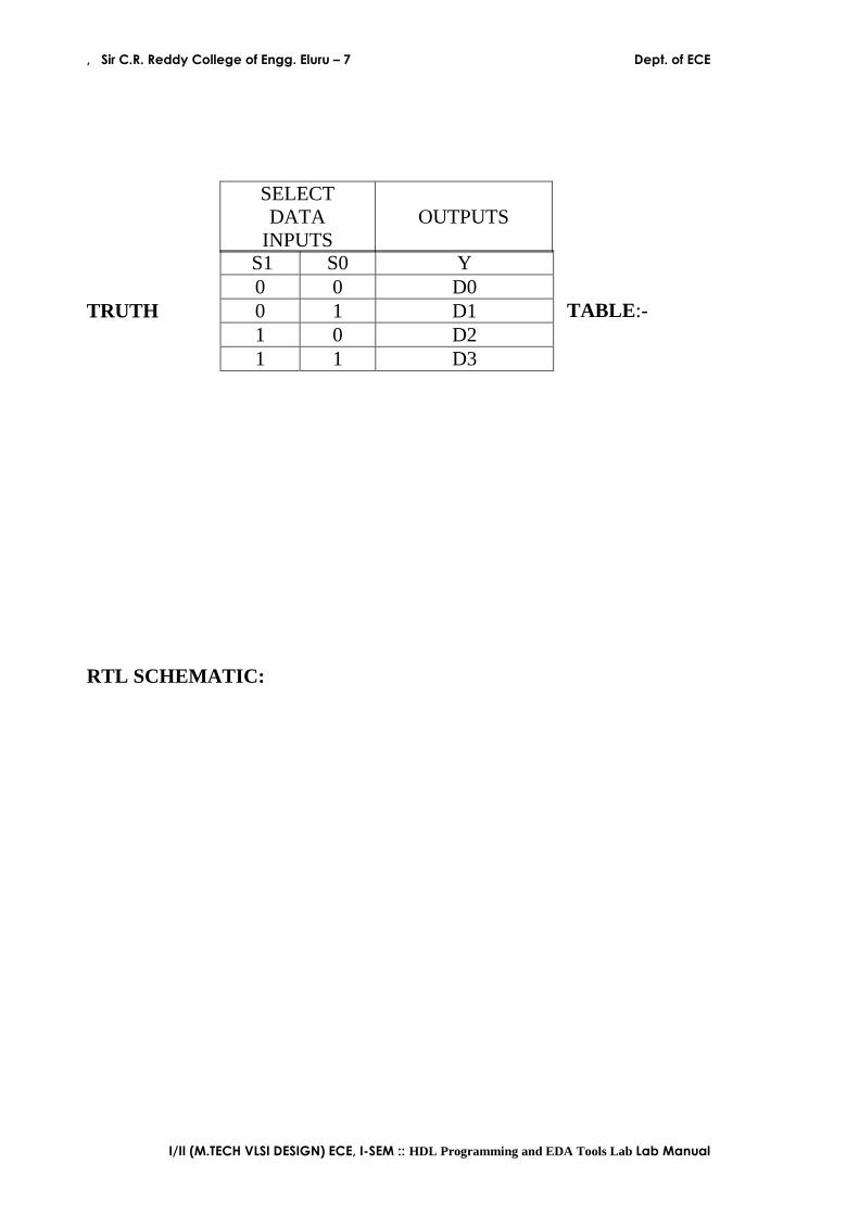
TRUTH TABLE :-
RTL SCHEMATIC:
SELECT DATA
INPUTS OUTPUTS
S1 S0 Y 0 0 D0 0 1 D1 1 0 D2 1 1 D3

, Sir C.R. Reddy College of Engg. Eluru – 7 Dept. of ECE
I/II (M.TECH VLSI DESIGN) ECE, I-SEM :: HDL Programming and EDA Tools Lab Lab Manual
WAVEFORMS:
MUX41

, Sir C.R. Reddy College of Engg. Eluru – 7 Dept. of ECE
I/II (M.TECH VLSI DESIGN) ECE, I-SEM :: HDL Programming and EDA Tools Lab Lab Manual
RESULT:- Hence the 4x1 multiplexer is implemented in VHDL and the
functionality is verified.
PREPARED BY: CHECKED BY: H.O.D:
, Sir C.R. Reddy College of Engg. Eluru – 7 Dept. of ECE
I/II (M.TECH VLSI DESIGN) ECE, I-SEM :: HDL Programming and EDA Tools Lab Lab Manual
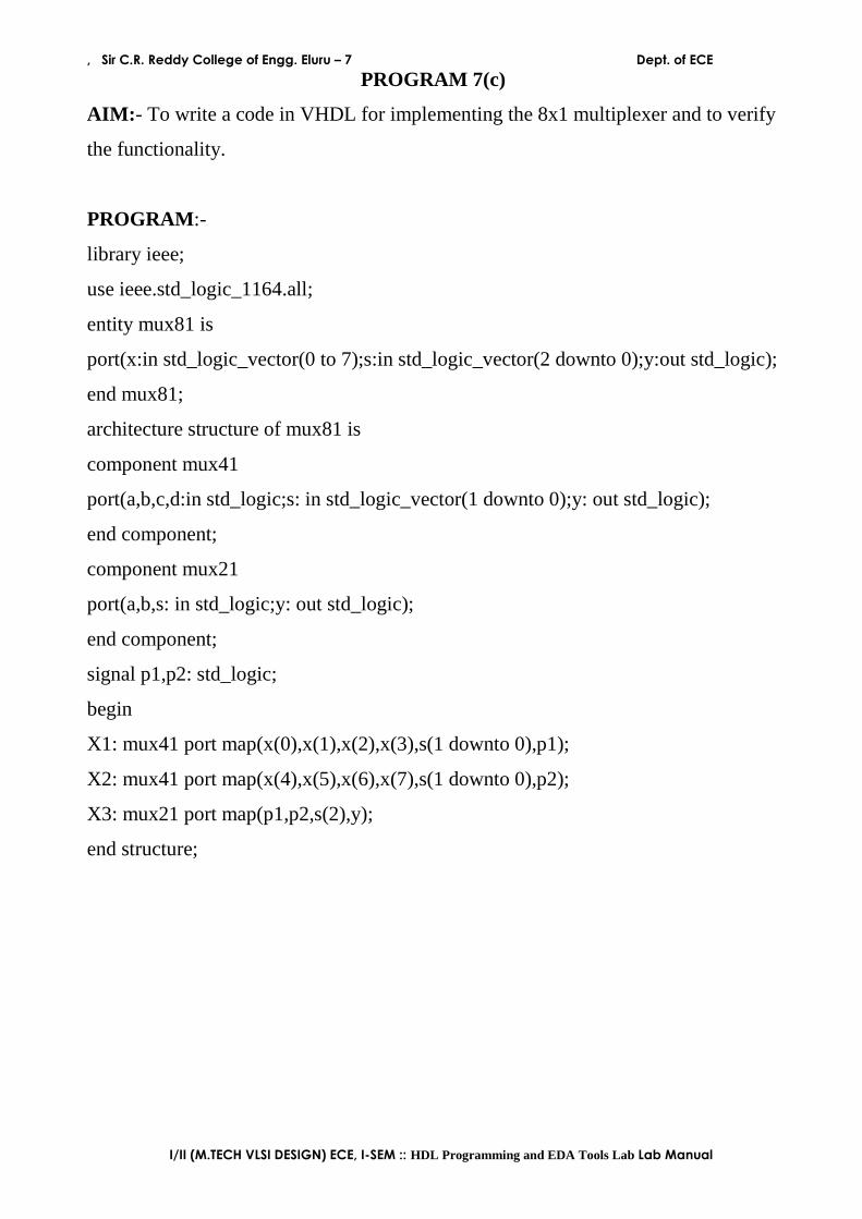
PROGRAM 7(c)
AIM: - To write a code in VHDL for implementing the 8x1 multiplexer and to verify
the functionality.
PROGRAM :-
library ieee;
use ieee.std_logic_1164.all;
entity mux81 is
port(x:in std_logic_vector(0 to 7);s:in std_logic_vector(2 downto 0);y:out std_logic);
end mux81;
architecture structure of mux81 is
component mux41
port(a,b,c,d:in std_logic;s: in std_logic_vector(1 downto 0);y: out std_logic);
end component;
component mux21
port(a,b,s: in std_logic;y: out std_logic);
end component;
signal p1,p2: std_logic;
begin
X1: mux41 port map(x(0),x(1),x(2),x(3),s(1 downto 0),p1);
X2: mux41 port map(x(4),x(5),x(6),x(7),s(1 downto 0),p2);
X3: mux21 port map(p1,p2,s(2),y);
end structure;

, Sir C.R. Reddy College of Engg. Eluru – 7 Dept. of ECE
I/II (M.TECH VLSI DESIGN) ECE, I-SEM :: HDL Programming and EDA Tools Lab Lab Manual
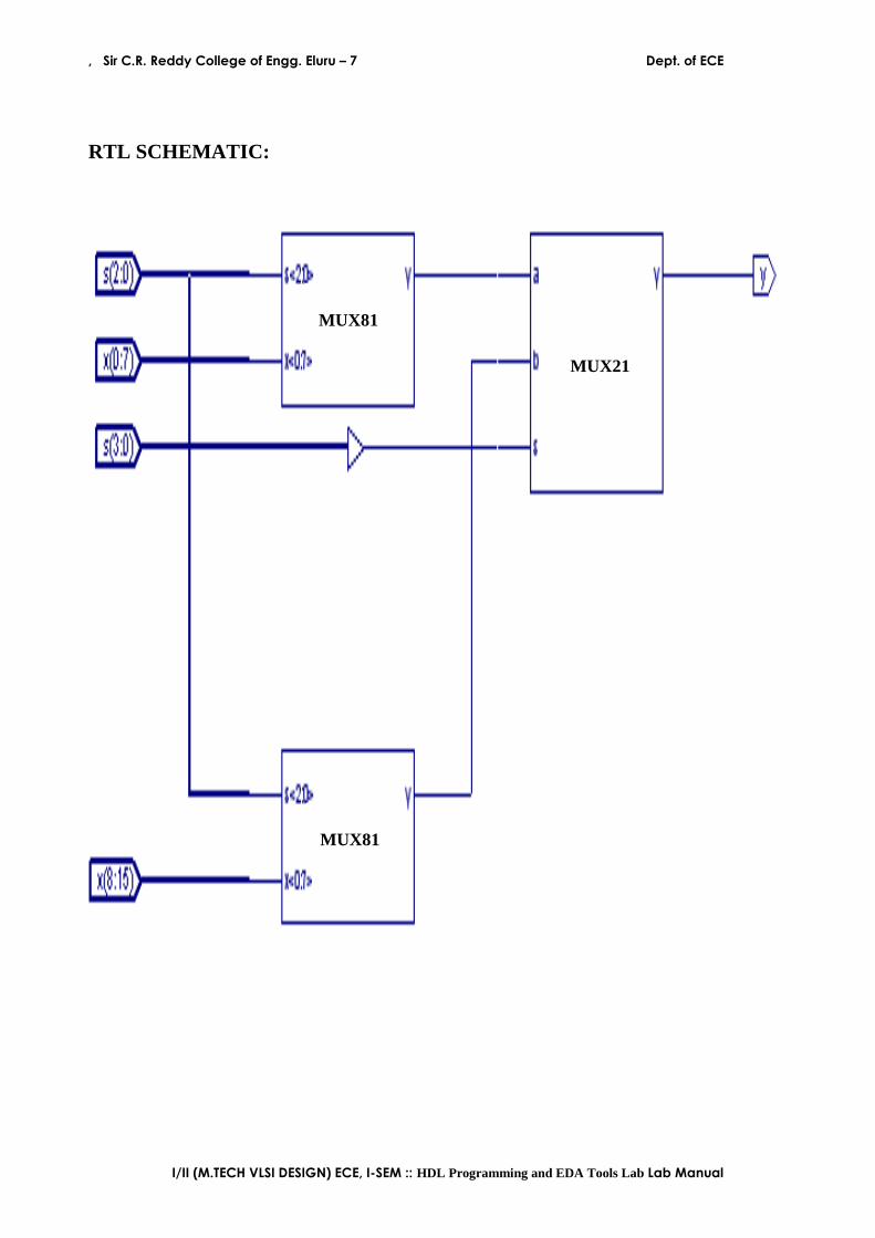
RTL SCHEMATIC:
MUX41
MUX41
MUX21
, Sir C.R. Reddy College of Engg. Eluru – 7 Dept. of ECE
I/II (M.TECH VLSI DESIGN) ECE, I-SEM :: HDL Programming and EDA Tools Lab Lab Manual
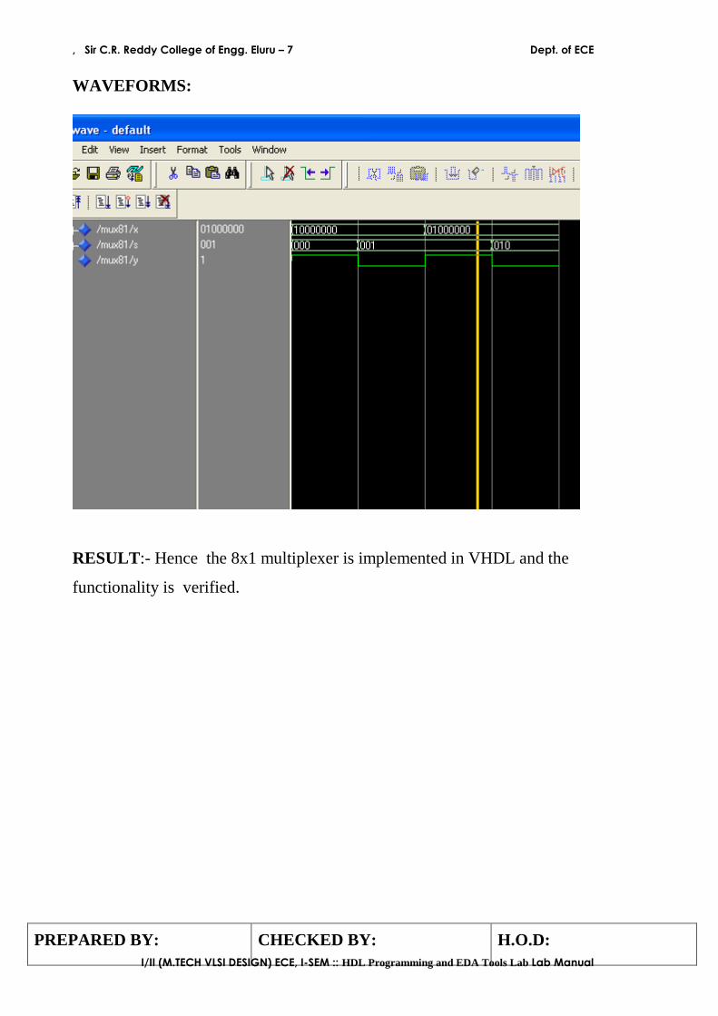
WAVEFORMS:
RESULT:- Hence the 8x1 multiplexer is implemented in VHDL and the
functionality is verified.
PREPARED BY: CHECKED BY: H.O.D:

, Sir C.R. Reddy College of Engg. Eluru – 7 Dept. of ECE
I/II (M.TECH VLSI DESIGN) ECE, I-SEM :: HDL Programming and EDA Tools Lab Lab Manual
PROGRAM 7(d)
AIM: - To write a code in VHDL for implementing the 16x1 multiplexer and to
observe the waveforms.
PROGRAM :-
library ieee;
use ieee.std_logic_1164.all;
entity mux16_1 is
port(x:in std_logic_vector(0 to 15);s:in std_logic_vector(3 downto 0);y:out
std_logic);
end mux16_1;
architecture structure of mux16_1 is
component mux81
port(x:in std_logic_vector(0 to 7);s:in std_logic_vector(2 downto 0);y:out std_logic);
end component;
component mux21
port(a,b,s: in std_logic;y: out std_logic);
end component;
signal p1,p2: std_logic;
begin
X1: mux81 port map(x(0 to 7),s(2 downto 0),p1);
X2: mux81 port map(x(8 to 15),s(2 downto 0),p2);
X3: mux21 port map(p1,p2,s(3),y);
end structure;
, Sir C.R. Reddy College of Engg. Eluru – 7 Dept. of ECE
I/II (M.TECH VLSI DESIGN) ECE, I-SEM :: HDL Programming and EDA Tools Lab Lab Manual
RTL SCHEMATIC:
MUX81
MUX81
MUX21

, Sir C.R. Reddy College of Engg. Eluru – 7 Dept. of ECE
I/II (M.TECH VLSI DESIGN) ECE, I-SEM :: HDL Programming and EDA Tools Lab Lab Manual
WAVEFORMS:
RESULT:- Hence the 16x1 multiplexer is implemented in VHDL and the
functionality is verified.
PREPARED BY: CHECKED BY: H.O.D:

, Sir C.R. Reddy College of Engg. Eluru – 7 Dept. of ECE
I/II (M.TECH VLSI DESIGN) ECE, I-SEM :: HDL Programming and EDA Tools Lab Lab Manual
PROGRAM 7(e) AIM: - To write a code in VHDL for implementing the 64x1 multiplexer and to
verify the functionality.
PROGRAM :-
library ieee;
use ieee.std_logic_1164.all;
entity mux64_1 is
port(x:in std_logic_vector(0 to 63);s:in std_logic_vector(5 downto 0);y:out
std_logic);
end mux64_1;
architecture structure of mux64_1 is
component mux16_1
port(x:in std_logic_vector(0 to 15);s:in std_logic_vector(3 downto 0);y:out
std_logic);
end component;
component mux41
port(a,b,c,d:in std_logic;s:in std_logic_vector(1 downto 0);y:out std_logic);
end component;
signal p1,p2,p3,p4: std_logic;
begin
X1: mux16_1 port map(x(0 to 15),s(3 downto 0),p1);
X2: mux16_1 port map(x(16 to 31),s(3 downto 0),p2);
X3: mux16_1 port map(x(32 to 47),s(3 downto 0),p3);
X4: mux16_1 port map(x(48 to 63),s(3 downto 0),p4);
X5: mux41 port map(p1,p2,p3,p4,s(5 downto 4),y);
end structure;
, Sir C.R. Reddy College of Engg. Eluru – 7 Dept. of ECE
I/II (M.TECH VLSI DESIGN) ECE, I-SEM :: HDL Programming and EDA Tools Lab Lab Manual
RTL SCHEMATIC:

, Sir C.R. Reddy College of Engg. Eluru – 7 Dept. of ECE
I/II (M.TECH VLSI DESIGN) ECE, I-SEM :: HDL Programming and EDA Tools Lab Lab Manual
MUX16_1
MUX16_1
MUX16_1
MUX41
MUX16_1

, Sir C.R. Reddy College of Engg. Eluru – 7 Dept. of ECE
I/II (M.TECH VLSI DESIGN) ECE, I-SEM :: HDL Programming and EDA Tools Lab Lab Manual
WAVEFORMS:
RESULT:- Hence the 64x1 multiplexer is implemented in VHDL and the
functionality is verified.
PREPARED BY: CHECKED BY: H.O.D:

, Sir C.R. Reddy College of Engg. Eluru – 7 Dept. of ECE
I/II (M.TECH VLSI DESIGN) ECE, I-SEM :: HDL Programming and EDA Tools Lab Lab Manual
PROGRAM-8

, Sir C.R. Reddy College of Engg. Eluru – 7 Dept. of ECE
I/II (M.TECH VLSI DESIGN) ECE, I-SEM :: HDL Programming and EDA Tools Lab Lab Manual
PROGRAM 8(a)
AIM: - To write a code in VHDL for implementing the 4 to 2 encoder and to verify
the functionality.
PROGRAM :-
library ieee;
use ieee.std_logic_1164.all;
entity e42 is
port(p: in std_logic_vector(3 downto 0);y: out std_logic_vector(1 downto 0));
end e42;
architecture beh of e42 is
begin
process(p)
begin
case p is
when "0001"=>y<="00";
when "0010"=>y<="01";
when "0100"=>y<="10";
when "1000"=>y<="11";
when others=>y<="UU";
end case;
end process;
end beh;
TRUTH TABLE :-
INPUTS OUTPUTS
P3 P2 P1 P0 Y1 Y0 0 0 0 1 0 0 0 0 1 0 0 1 0 1 0 0 1 0 1 0 0 0 1 1

, Sir C.R. Reddy College of Engg. Eluru – 7 Dept. of ECE
I/II (M.TECH VLSI DESIGN) ECE, I-SEM :: HDL Programming and EDA Tools Lab Lab Manual
RTL SCHEMATIC:
WAVEFORMS:
RESULT:- Hence the 4 to 2 encoder is implemented in VHDL and the functionality
is verified.
4 TO 2 ENCODER
P(3) P(2) P(1) P(0)
Y(1) Y(0)

, Sir C.R. Reddy College of Engg. Eluru – 7 Dept. of ECE
I/II (M.TECH VLSI DESIGN) ECE, I-SEM :: HDL Programming and EDA Tools Lab Lab Manual
PROGRAM 8(b)
AIM: - To write a code in VHDL for implementing the 8 to 3 encoder and to verify
the functionality.
PROGRAM :-
library ieee;
use ieee.std_logic_1164.all;
entity e83 is
port(p: in std_logic_vector(7 downto 0);y: out std_logic_vector(2 downto 0));
end e83;
architecture beh of e83 is
begin
process(p)
begin
case p is
when "00000001"=>y<="000";
when "00000010"=>y<="001";
when "00000100"=>y<="010";
when "00001000"=>y<="011";
when "00010000"=>y<="100";
when "00100000"=>y<="101";
when "01000000"=>y<="110";
when "10000000"=>y<="111";
when others=>y<="UUU";
end case;
end process;
end beh;
PREPARED BY: CHECKED BY: H.O.D:

, Sir C.R. Reddy College of Engg. Eluru – 7 Dept. of ECE
I/II (M.TECH VLSI DESIGN) ECE, I-SEM :: HDL Programming and EDA Tools Lab Lab Manual
TRUTH TABLE:-
RTL SCHEMATIC:
INPUTS OUTPUTS
P7 P6 P5 P4 P3 P2 P1 P0 Y(2) Y(1) Y(0) 0 0 0 0 0 0 0 1 0 0 0 0 0 0 0 0 0 1 0 0 0 1 0 0 0 0 0 1 0 0 0 1 0 0 0 0 0 1 0 0 0 0 1 1 0 0 0 1 0 0 0 0 1 0 0 0 0 1 0 0 0 0 0 1 0 1 0 1 0 0 0 0 0 0 1 1 0 1 0 0 0 0 0 0 0 1 1 1
8 TO 3 ENCODER
P(7) P(6) P(5) P(4) P(3) P(2) P(1) P(0)
Y(2) Y(1) Y(0)

, Sir C.R. Reddy College of Engg. Eluru – 7 Dept. of ECE
I/II (M.TECH VLSI DESIGN) ECE, I-SEM :: HDL Programming and EDA Tools Lab Lab Manual
WAVEFORMS:
RESULT:- Hence the 8 to 3 encoder is implemented in VHDL and the functionality
is verified.

, Sir C.R. Reddy College of Engg. Eluru – 7 Dept. of ECE
I/II (M.TECH VLSI DESIGN) ECE, I-SEM :: HDL Programming and EDA Tools Lab Lab Manual
PROGRAM -9
PREPARED BY: CHECKED BY: H.O.D:

, Sir C.R. Reddy College of Engg. Eluru – 7 Dept. of ECE
I/II (M.TECH VLSI DESIGN) ECE, I-SEM :: HDL Programming and EDA Tools Lab Lab Manual
PROGRAM -9
AIM: - To write a code in VHDL for implementing the 1x8 demultiplexer and to
verify the functionality.
PROGRAM :-
use ieee.std_logic_1164.all;
entity dmux81 is
port(a: in std_logic;s: in std_logic_vector(2 downto 0);y: out std_logic_vector(0 to
7));
end dmux81;
architecture dmux of dmux81 is
begin
process(a,s)
begin
y<="00000000";
case s is
when "000"=>y(0)<=a;
when "001"=>y(1)<=a;
when "010"=>y(2)<=a;
when "011"=>y(3)<=a;
when "100"=>y(4)<=a;
when "101"=>y(5)<=a;

, Sir C.R. Reddy College of Engg. Eluru – 7 Dept. of ECE
I/II (M.TECH VLSI DESIGN) ECE, I-SEM :: HDL Programming and EDA Tools Lab Lab Manual
when "110"=>y(6)<=a;
when "111"=>y(7)<=a;
when others=>y<="UUUUUUUU";
end case;
end process;
end dmux;
TRUTH TABLE :-
DATA INPUT
SELECT INPUTS
OUTPUTS
a S2 S1 S0 Y0 Y1 Y2 Y3 Y4 Y5 Y6 Y7 a 0 0 0 a 0 0 0 0 0 0 0 a 0 0 1 0 a 0 0 0 0 0 0 a 0 1 0 0 0 a 0 0 0 0 0 a 0 1 1 0 0 0 a 0 0 0 0 a 1 0 0 0 0 0 0 a 0 0 0 a 1 0 1 0 0 0 0 0 a 0 0 a 1 1 0 0 0 0 0 0 0 a 0 a 1 1 1 0 0 0 0 0 0 0 a
RTL SCHEMATIC:

, Sir C.R. Reddy College of Engg. Eluru – 7 Dept. of ECE
I/II (M.TECH VLSI DESIGN) ECE, I-SEM :: HDL Programming and EDA Tools Lab Lab Manual
WAVEFORMS:
DMUX81

, Sir C.R. Reddy College of Engg. Eluru – 7 Dept. of ECE
I/II (M.TECH VLSI DESIGN) ECE, I-SEM :: HDL Programming and EDA Tools Lab Lab Manual
RESULT:- Hence the 8x1 multiplexer is implemented in VHDL and the
functionality is verified.
PREPARED BY: CHECKED BY: H.O.D:

, Sir C.R. Reddy College of Engg. Eluru – 7 Dept. of ECE
I/II (M.TECH VLSI DESIGN) ECE, I-SEM :: HDL Programming and EDA Tools Lab Lab Manual
PROGRAM-10

, Sir C.R. Reddy College of Engg. Eluru – 7 Dept. of ECE
I/II (M.TECH VLSI DESIGN) ECE, I-SEM :: HDL Programming and EDA Tools Lab Lab Manual
PROGRAM 10(a)
AIM: - To write a code in VHDL for implementing the two bit comparator and to
verify the functionality.
PROGRAM :-
library ieee;
use ieee.std_logic_1164.all;
entity comp2 is
port(a,b: in std_logic_vector(1 downto 0);eq,le,gr: out boolean);
end comp2;
architecture comp of comp2 is
begin
eq<=(a=b);
le<=(a<b);
gr<=(a>b);
end comp;
TRUTH TABLE :-
A1 A0 B1 B0 A>B A=B A<B 0 0 0 0 0 1 0 0 0 0 1 0 0 1 0 0 1 0 0 0 1 0 0 1 1 0 0 1 0 1 0 0 1 0 0 0 1 0 1 0 1 0 0 1 1 0 0 0 1 0 1 1 1 0 0 1 1 0 0 0 1 0 0 1 0 0 1 1 0 0 1 0 1 0 0 1 0 1 0 1 1 0 0 1 1 1 0 0 1 0 0 1 1 0 1 1 0 0 1 1 1 0 1 0 0 1 1 1 1 0 1 0
INPUTS OUTPUTS

, Sir C.R. Reddy College of Engg. Eluru – 7 Dept. of ECE
I/II (M.TECH VLSI DESIGN) ECE, I-SEM :: HDL Programming and EDA Tools Lab Lab Manual
RTL SCHEMATIC:
WAVEFORMS:
RESULT:- Hence the two bit comparator is implemented in VHDL and the
functionality is verified.
COMP2

, Sir C.R. Reddy College of Engg. Eluru – 7 Dept. of ECE
I/II (M.TECH VLSI DESIGN) ECE, I-SEM :: HDL Programming and EDA Tools Lab Lab Manual
PROGRAM 10(b)
AIM: - To write a code in VHDL for implementing the four bit comparator in
behavioural model and to verify the functionality.
PROGRAM:-
library ieee;
use ieee.std_logic_1164.all;
entity cmp4 is
port(a,b:in std_logic_vector(3 downto 0);eq,gt,lt:out std_logic);
end cmp4;
architecture behaviour of cmp4 is
begin
process(a,b)
begin
for i in 3 downto 0 loop
if(a(i)>b(i)) then
gt<='1';
lt<='0';
eq<='0';
exit;
elsif(a(i)<b(i)) then
gt<='0';
eq<='0';
lt<='1';
exit;
else
eq<='1';gt<='0';lt<='0';
end if;
PREPARED BY: CHECKED BY: H.O.D:

, Sir C.R. Reddy College of Engg. Eluru – 7 Dept. of ECE
I/II (M.TECH VLSI DESIGN) ECE, I-SEM :: HDL Programming and EDA Tools Lab Lab Manual
end loop;
end process;
end behaviour;
TRUTH TABLE :-
RTL SCHEMATIC:
COMPARING INPUTS OUTPUTS
A3,B3 A2,B2 A1,B1 A0,B0 A>B A<B A=B A3>B3 X X X 1 0 0 A3<B3 X X X 0 1 0 A3=B3 A2>B2 X X 1 0 0 A3=B3 A2<B2 X X 0 1 0 A3=B3 A2=B2 A1>B1 X 1 0 0 A3=B3 A2=B2 A1<B1 X 0 1 0 A3=B3 A2=B2 A1=B1 A0>B0 1 0 0 A3=B3 A2=B2 A1=B1 A0<B0 0 1 0
CMP4

, Sir C.R. Reddy College of Engg. Eluru – 7 Dept. of ECE
I/II (M.TECH VLSI DESIGN) ECE, I-SEM :: HDL Programming and EDA Tools Lab Lab Manual
WAVEFORMS:
RESULT:- Hence the four bit comparator in behavioural model is implemented in
VHDL and the functionality is verified.
PREPARED BY: CHECKED BY: H.O.D:

, Sir C.R. Reddy College of Engg. Eluru – 7 Dept. of ECE
I/II (M.TECH VLSI DESIGN) ECE, I-SEM :: HDL Programming and EDA Tools Lab Lab Manual
PROGRAM-11

, Sir C.R. Reddy College of Engg. Eluru – 7 Dept. of ECE
I/II (M.TECH VLSI DESIGN) ECE, I-SEM :: HDL Programming and EDA Tools Lab Lab Manual
PROGRAM 11(a)
AIM: - To write a code in VHDL for implementing the SR flip-flop and to verify the
functionality.
PROGRAM:-
library ieee;
use ieee.std_logic_1164.all;
entity SR is
port(S,R,clk: in std_logic;Q:inout std_logic:='0';Qb:inout std_logic:='1');
end SR;
architecture ff of SR is
begin
process(S,R,clk)
variable t,tb: std_logic;
begin
t:=Q;
tb:=Qb;
if (clk='0'and clk'event) then
if(S='0'and R='0') then t:=t;tb:=tb;
elsif(S='0'and R='1') then t:='0';tb:='1';
elsif(S='1'and R='0') then t:='1';tb:='0';
elsif(S='1'and R='1') then t:='U';tb:='U';
end if;
Q<=t;
Qb<=tb;
end if;

, Sir C.R. Reddy College of Engg. Eluru – 7 Dept. of ECE
I/II (M.TECH VLSI DESIGN) ECE, I-SEM :: HDL Programming and EDA Tools Lab Lab Manual
end process;
end ff;
TRUTH TABLE :-
RTL SCHEMATIC:
INPUTS OUTPUTS
S R Q Qb
0 0 Q Qb
0 1 0 1
1 0 1 0
1 1 X X
SR FLIPFLOP
S R CLK
Q Qb

, Sir C.R. Reddy College of Engg. Eluru – 7 Dept. of ECE
I/II (M.TECH VLSI DESIGN) ECE, I-SEM :: HDL Programming and EDA Tools Lab Lab Manual
WAVEFORMS:
RESULT:- Hence the SR flip-flop is implemented in VHDL and the functionality is
verified.
, Sir C.R. Reddy College of Engg. Eluru – 7 Dept. of ECE
I/II (M.TECH VLSI DESIGN) ECE, I-SEM :: HDL Programming and EDA Tools Lab Lab Manual
PROGRAM 11(b)
AIM: - To write a code in VHDL for implementing the JK flip-flop and to verify the
functionality.
PROGRAM:-
library ieee;
use ieee.std_logic_1164.all;
entity JK is
port(J,K,clk: in std_logic;Q:inout std_logic:='0';Qb:inout std_logic:='1');
end JK;
architecture ff of JK is
begin
process(J,K,clk)
variable t,tb: std_logic;
begin
t:=Q;
tb:=Qb;
if (clk='0'and clk'event) then
if(J='0'and K='0') then t:=t;tb:=tb;
elsif(J='0'and K='1') then t:='0';tb:='1';
elsif(J='1'and K='0') then t:='1';tb:='0';
elsif(J='1'and K='1') then t:=not t;tb:=not tb;
PREPARED BY: CHECKED BY: H.O.D:

, Sir C.R. Reddy College of Engg. Eluru – 7 Dept. of ECE
I/II (M.TECH VLSI DESIGN) ECE, I-SEM :: HDL Programming and EDA Tools Lab Lab Manual
end if;
end if;
Q<=t;
Qb<=tb;
end process;
end ff;
TRUTH TABLE :- RTL SCHEMATIC:
INPUTS OUTPUTS
J K Q Qb
0 0 Q Qb
0 1 0 1
1 0 1 0
1 1 Q Qb
JK FLIPFLOP
J K CLK
Q Qb

, Sir C.R. Reddy College of Engg. Eluru – 7 Dept. of ECE
I/II (M.TECH VLSI DESIGN) ECE, I-SEM :: HDL Programming and EDA Tools Lab Lab Manual
WAVEFORMS:
RESULT:- Hence the JK flip-flop is implemented in VHDL and the functionality is
verified.

, Sir C.R. Reddy College of Engg. Eluru – 7 Dept. of ECE
I/II (M.TECH VLSI DESIGN) ECE, I-SEM :: HDL Programming and EDA Tools Lab Lab Manual
PROGRAM 11(c)
AIM: - To write a code in VHDL for implementing the D flip-flop and to to verify
the functionality.
PROGRAM:-
library ieee;
use ieee.std_logic_1164.all;
entity d_ff is
port(d,clk:in std_logic; Q:inout std_logic:='0';Qb:inout std_logic:='1’);
end d_ff;
architecture behaviour of d_ff is
begin
process(d,clk)
begin
if (clk='0' and clk'event)then
q<=d;
qb<=not(d);
end if;
end process;
end behaviour;
PREPARED BY: CHECKED BY: H.O.D:

, Sir C.R. Reddy College of Engg. Eluru – 7 Dept. of ECE
I/II (M.TECH VLSI DESIGN) ECE, I-SEM :: HDL Programming and EDA Tools Lab Lab Manual
TRUTH TABLE :-
RTL SCHEMATIC:
WAVEFORMS:
INPUTS OUTPUTS
D Q Qb
0 0 1
1 1 0
D_FF

, Sir C.R. Reddy College of Engg. Eluru – 7 Dept. of ECE
I/II (M.TECH VLSI DESIGN) ECE, I-SEM :: HDL Programming and EDA Tools Lab Lab Manual
RESULT:- Hence the D flip-flop is implemented in VHDL and the functionality is
verified.
PROGRAM 11(d)
AIM: - To write a code in VHDL for implementing the T flip-flop and to verify the
functionality.
PROGRAM:-
COMPONENT JK:-
library ieee;
use ieee.std_logic_1164.all;
entity JK is
port(J,K,clk: in std_logic;Q:inout std_logic:='0';Qb:inout std_logic:='1');
PREPARED BY: CHECKED BY: H.O.D:

, Sir C.R. Reddy College of Engg. Eluru – 7 Dept. of ECE
I/II (M.TECH VLSI DESIGN) ECE, I-SEM :: HDL Programming and EDA Tools Lab Lab Manual
end JK;
architecture ff of JK is
begin
process(J,K,clk)
variable t,tb: std_logic;
begin
t:=Q;
tb:=Qb;
if (clk='0'and clk'event) then
if(J='0'and K='0') then t:=t;tb:=tb;
elsif(J='0'and K='1') then t:='0';tb:='1';
elsif(J='1'and K='0') then t:='1';tb:='0';
elsif(J='1'and K='1') then t:=not t;tb:=not tb;
end if;
end if;
Q<=t;
Qb<=tb;
end process;
end ff;
TOP MODULE:-
library ieee;
use ieee.std_logic_1164.all;
entity T is
port(T,clk: in std_logic;Q:inout std_logic:='0';Qb:inout std_logic:='1');
end T;
architecture ff of T is
component JK
port(J,K,clk: in std_logic;Q:inout std_logic:='0';Qb:inout std_logic:='1');

, Sir C.R. Reddy College of Engg. Eluru – 7 Dept. of ECE
I/II (M.TECH VLSI DESIGN) ECE, I-SEM :: HDL Programming and EDA Tools Lab Lab Manual
end component;
begin
X1: JK port map(T,T,clk,Q,Qb);
end ff;
TRUTH TABLE :- RTL SCHEMATIC:
WAVEFORMS:
INPUTS OUTPUTS
T Q Qb
0 Q Qb
1 Qb Q
J T FLIPFLOP K
T
Q Qb
CLK

, Sir C.R. Reddy College of Engg. Eluru – 7 Dept. of ECE
I/II (M.TECH VLSI DESIGN) ECE, I-SEM :: HDL Programming and EDA Tools Lab Lab Manual
RESULT:- Hence the T flip-flop is implemented in VHDL and the functionality is
verified.
PREPARED BY: CHECKED BY: H.O.D:

, Sir C.R. Reddy College of Engg. Eluru – 7 Dept. of ECE
I/II (M.TECH VLSI DESIGN) ECE, I-SEM :: HDL Programming and EDA Tools Lab Lab Manual
PROGRAM-12

, Sir C.R. Reddy College of Engg. Eluru – 7 Dept. of ECE
I/II (M.TECH VLSI DESIGN) ECE, I-SEM :: HDL Programming and EDA Tools Lab Lab Manual
PROGRAM 12(a)
AIM: - To write a code in VHDL for implementing the decade counter using
structural model and to verify the functionality.
PROGRAM:-
COMPONENT JK:-
library ieee;
use ieee.std_logic_1164.all;
entity JK is
port(J,K,clk: in std_logic;Q:inout std_logic:='0';Qb:inout std_logic:='1');
end JK;
architecture ff of JK is
begin
process(J,K,clk)
variable t,tb: std_logic;
begin
t:=Q;
tb:=Qb;
if (clk='0'and clk'event) then
if(J='0'and K='0') then t:=t;tb:=tb;
elsif(J='0'and K='1') then t:='0';tb:='1';
elsif(J='1'and K='0') then t:='1';tb:='0';
elsif(J='1'and K='1') then t:=not t;tb:=not tb;
end if;
end if;
Q<=t;
Qb<=tb;
end process;

, Sir C.R. Reddy College of Engg. Eluru – 7 Dept. of ECE
I/II (M.TECH VLSI DESIGN) ECE, I-SEM :: HDL Programming and EDA Tools Lab Lab Manual
end ff;
TOP MODULE:-
library ieee;
use ieee.std_logic_1164.all;
entity dec_counter is
port(clock:in std_logic;z: inout std_logic_vector(3 downto 0):="0000");
end dec_counter;
architecture counter of dec_counter is
component JK
port(J,K,clk: in std_logic;Q:inout std_logic:='0';Qb:inout std_logic:='1');
end component;
component and2
port(a,b:in std_logic;c:out std_logic);
end component;
signal s1,s2:std_logic;
signal s:std_logic:='1';
begin
JK1: JK port map(s,s,clock,z(0),open);
JK2: JK port map(s2,s,z(0),z(1),open);
JK3: JK port map(s,s,z(1),z(2),open);
X1: and2 port map(z(2),z(1),s1);
JK4: JK port map(s1,s,z(0),z(3),s2);
end counter;

, Sir C.R. Reddy College of Engg. Eluru – 7 Dept. of ECE
I/II (M.TECH VLSI DESIGN) ECE, I-SEM :: HDL Programming and EDA Tools Lab Lab Manual
TRUTH TABLE :-
RTL SCHEMATIC:
PRESENT STATE NEXT STATE
q3 q2 q1 q0 Q3 Q2 Q1 Q0 0 0 0 0 0 0 0 1 0 0 0 1 0 0 1 0 0 0 1 0 0 0 1 1 0 0 1 1 0 1 0 0 0 1 0 0 0 1 0 1 0 1 0 1 0 1 1 0 0 1 1 0 0 1 1 1 0 1 1 1 1 0 0 0 1 0 0 0 1 0 0 1 1 0 0 1 0 0 0 0 1 0 1 0 X X X X 1 0 1 1 X X X X 1 1 0 0 X X X X 1 1 0 1 X X X X 1 1 1 0 X X X X 1 1 1 1 X X X X

, Sir C.R. Reddy College of Engg. Eluru – 7 Dept. of ECE
I/II (M.TECH VLSI DESIGN) ECE, I-SEM :: HDL Programming and EDA Tools Lab Lab Manual
WAVEFORMS:
RESULT:- Hence decade counter using structural model is implemented in VHDL
and the functionality is verified.
DEC_COUNTER
CLK
Z(3) Z(2) Z(1) Z(0)

, Sir C.R. Reddy College of Engg. Eluru – 7 Dept. of ECE
I/II (M.TECH VLSI DESIGN) ECE, I-SEM :: HDL Programming and EDA Tools Lab Lab Manual
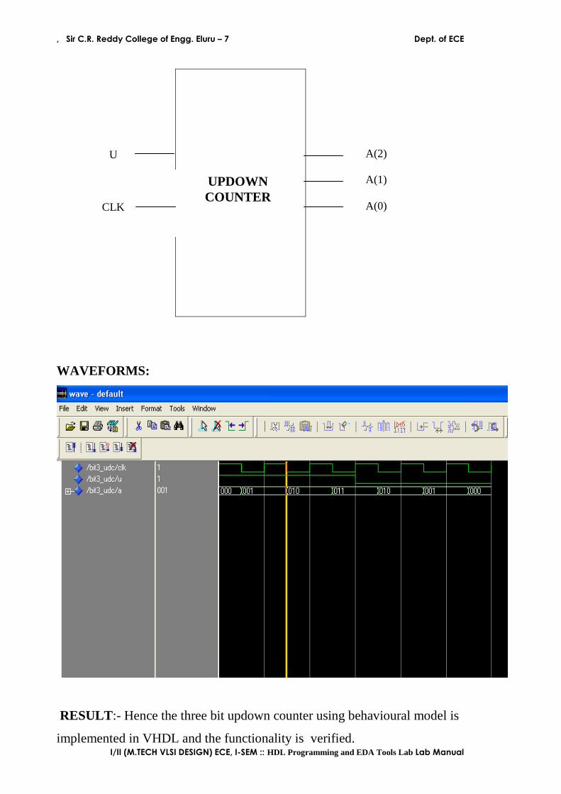
PROGRAM 12(b)
AIM: - To write a code in VHDL for implementing the three bit updown counter
using behavioural model and to verify the functionality.
PROGRAM:-
library ieee;
use ieee.std_logic_1164.all;
use ieee.std_logic_arith.all;
use ieee.std_logic_unsigned.all;
entity bit3_udc is
port(clk,u:in std_logic;a: inout std_logic_vector(2 downto 0):="000");
end bit3_udc;
architecture beh of bit3_udc is
begin
process(clk,a,u)
variable t: std_logic_vector(2 downto 0);
begin
PREPARED BY: CHECKED BY: H.O.D:

, Sir C.R. Reddy College of Engg. Eluru – 7 Dept. of ECE
I/II (M.TECH VLSI DESIGN) ECE, I-SEM :: HDL Programming and EDA Tools Lab Lab Manual
t:=a;
if clk='0' and clk'event then
if u='1' then t:= t+"001";
elsif u='0' then t:= t+"111";
end if;
end if;
a<=t;
end process;
end beh;
TRUTH TABLE :-
UP/DOWN q2 q1 q0 Q2 Q1 Q0 0 0 0 0 1 1 1 0 0 0 1 0 0 0 0 0 1 0 0 0 1 0 0 1 1 0 1 0 0 1 0 0 0 1 1 0 1 0 1 1 0 0 0 1 1 0 1 0 1 0 1 1 1 1 1 0 1 0 0 0 0 0 1 1 0 0 1 0 1 0 1 0 1 0 0 1 1 1 0 1 1 1 0 0 1 1 0 0 1 0 1 1 1 0 1 1 1 0 1 1 1 0 1 1 1 1 1 1 1 0 0 0
RTL SCHEMATIC:
INPUT PRESENT
STATE NEXT STATE
, Sir C.R. Reddy College of Engg. Eluru – 7 Dept. of ECE
I/II (M.TECH VLSI DESIGN) ECE, I-SEM :: HDL Programming and EDA Tools Lab Lab Manual
WAVEFORMS:
RESULT:- Hence the three bit updown counter using behavioural model is
implemented in VHDL and the functionality is verified.
UPDOWN COUNTER
U CLK
A(2)
A(1)
A(0)

, Sir C.R. Reddy College of Engg. Eluru – 7 Dept. of ECE
I/II (M.TECH VLSI DESIGN) ECE, I-SEM :: HDL Programming and EDA Tools Lab Lab Manual
PREPARED BY: CHECKED BY: H.O.D:
, Sir C.R. Reddy College of Engg. Eluru – 7 Dept. of ECE
I/II (M.TECH VLSI DESIGN) ECE, I-SEM :: HDL Programming and EDA Tools Lab Lab Manual
PROGRAM-13
PROGRAM 13(a)
AIM: - To write a code in VHDL for implementing the Serial In Serial Out(SISO)
and Serial In Parallel Out(SIPO) shift registers using single entity and multiple
architectures and to verify the functionality.
PROGRAM:-
COMPONENT D:-
library ieee;
use ieee.std_logic_1164.all;
entity D is
port(D,clk: in std_logic;Q:inout std_logic:='0');
end D;
architecture behaviour of D is

, Sir C.R. Reddy College of Engg. Eluru – 7 Dept. of ECE
I/II (M.TECH VLSI DESIGN) ECE, I-SEM :: HDL Programming and EDA Tools Lab Lab Manual
begin
process(D,clk)
begin
if (clk='0' and clk'event)then
Q<=D;
end if;
end process;
end behaviour;
TOP MODULE:-
library ieee;
use ieee.std_logic_1164.all;
entity siso_sipo is
port(si,clk: in std_logic;s0,p01,p02,p03,p04:inout std_logic);
end siso_sipo;
architecture siso_d of siso_sipo is
component D
port(D,clk: in std_logic;Q:inout std_logic:='0');
end component;
begin
D1: D port map(si,clk,p01);
D2: D port map(p01,clk,p02);

, Sir C.R. Reddy College of Engg. Eluru – 7 Dept. of ECE
I/II (M.TECH VLSI DESIGN) ECE, I-SEM :: HDL Programming and EDA Tools Lab Lab Manual
D3: D port map(p02,clk,p03);
D4: D port map(p03,clk,s0);
end siso_d;
architecture sipo_d of siso_sipo is
component D
port(D,clk: in std_logic;Q:inout std_logic:='0';Qb:inout std_logic:='1');
end component;
begin
D1: D port map(si,clk,p01);
D2: D port map(p01,clk,p02);
D3: D port map(p02,clk,p03);
D4: D port map(p03,clk,p04);
end sipo_d;
RTL SCHEMATIC:

, Sir C.R. Reddy College of Engg. Eluru – 7 Dept. of ECE
I/II (M.TECH VLSI DESIGN) ECE, I-SEM :: HDL Programming and EDA Tools Lab Lab Manual
WAVEFORMS:
D FF
D FF
D FF
D FF

, Sir C.R. Reddy College of Engg. Eluru – 7 Dept. of ECE
I/II (M.TECH VLSI DESIGN) ECE, I-SEM :: HDL Programming and EDA Tools Lab Lab Manual
RESULT:- Hence the Serial In Serial Out and Serial In Parallel Out shift registers
using single entity and multiple architectures is implemented in VHDL and the
functionality is verified.
PROGRAM 13(b)
PREPARED BY: CHECKED BY: H.O.D:

, Sir C.R. Reddy College of Engg. Eluru – 7 Dept. of ECE
I/II (M.TECH VLSI DESIGN) ECE, I-SEM :: HDL Programming and EDA Tools Lab Lab Manual
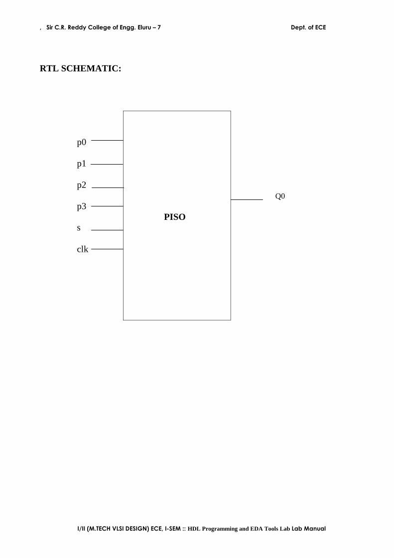
AIM: - To write a code in VHDL for implementing the Parallel In Serial Out shift
register(PISO) and to verify the functionality.
.
PROGRAM:-
COMPONENT D:-
library ieee;
use ieee.std_logic_1164.all;
entity D is
port(D,clk: in std_logic;Q:inout std_logic:='0';Qb:inout std_logic:='1');
end D;
architecture behaviour of D is
begin
process(D,clk)
begin
if (clk='0' and clk'event)then
Q<=D;
Qb<=not(D);
end if;
end process;
end behaviour;
COMPONENT OR2:-
library ieee;
use ieee.std_logic_1164.all;
entity or2 is
port(a,b: in std_logic;c: out std_logic);
end or2;
architecture dataflow of or2 is
begin
c<= a or b;
end dataflow;

, Sir C.R. Reddy College of Engg. Eluru – 7 Dept. of ECE
I/II (M.TECH VLSI DESIGN) ECE, I-SEM :: HDL Programming and EDA Tools Lab Lab Manual
COMPONENT AND2:-
library ieee;
use ieee.std_logic_1164.all;
entity and2 is
port(a,b: in std_logic;c: out std_logic);
end and2;
architecture dataflow of and2 is
begin
c<= a and b;
end dataflow;
COMPONENT NOT1:-
library ieee;
use ieee.std_logic_1164.all;
entity not1 is
port(a: in std_logic;c: out std_logic);
end not1;
architecture dataflow of not1 is
begin
c<= not(a);
end dataflow;
TOP MODULE:-
library ieee;
use ieee.std_logic_1164.all;
entity piso is
port(p0,p1,p2,p3,s,clk: in std_logic;Qo: inout std_logic);
end piso;
architecture piso of piso is
component D
port(D,clk: in std_logic;Q:inout std_logic:='0';Qb:inout std_logic:='1');

, Sir C.R. Reddy College of Engg. Eluru – 7 Dept. of ECE
I/II (M.TECH VLSI DESIGN) ECE, I-SEM :: HDL Programming and EDA Tools Lab Lab Manual
end component;
component and2
port(a,b: in std_logic;c: out std_logic);
end component;
component or2
port(a,b: in std_logic;c: out std_logic);
end component;
component not1
port(a: in std_logic;c: out std_logic);
end component;
signal s1,s2,s3,s4,s5,s6,s7,s8,s9,s10,q1,q2,q3: std_logic;
begin
n1: not1 port map(s,s1);
D1: D port map(p0,clk,q1,open);
a1: and2 port map(s,q1,s2);
a2: and2 port map(s1,p1,s3);
O1: or2 port map(s2,s3,s4);
D2: D port map(s4,clk,q2,open);
a3: and2 port map(s,q2,s5);
a4: and2 port map(s1,p2,s6);
O2: or2 port map(s5,s6,s7);
D3: D port map(s7,clk,q3,open);
a5: and2 port map(s,q3,s8);
a6: and2 port map(s1,p3,s9);
O3: or2 port map(s8,s9,s10);
D4: D port map(s10,clk,Qo,open);
end piso;
, Sir C.R. Reddy College of Engg. Eluru – 7 Dept. of ECE
I/II (M.TECH VLSI DESIGN) ECE, I-SEM :: HDL Programming and EDA Tools Lab Lab Manual
RTL SCHEMATIC:
p0 p1 p2 p3 s clk
Q0
PISO

, Sir C.R. Reddy College of Engg. Eluru – 7 Dept. of ECE
I/II (M.TECH VLSI DESIGN) ECE, I-SEM :: HDL Programming and EDA Tools Lab Lab Manual
WAVEFORMS:
RESULT:- Hence the Parallel In Serial Out shift register(PISO) is implemented in
VHDL and the functionality is verified.
, Sir C.R. Reddy College of Engg. Eluru – 7 Dept. of ECE
I/II (M.TECH VLSI DESIGN) ECE, I-SEM :: HDL Programming and EDA Tools Lab Lab Manual
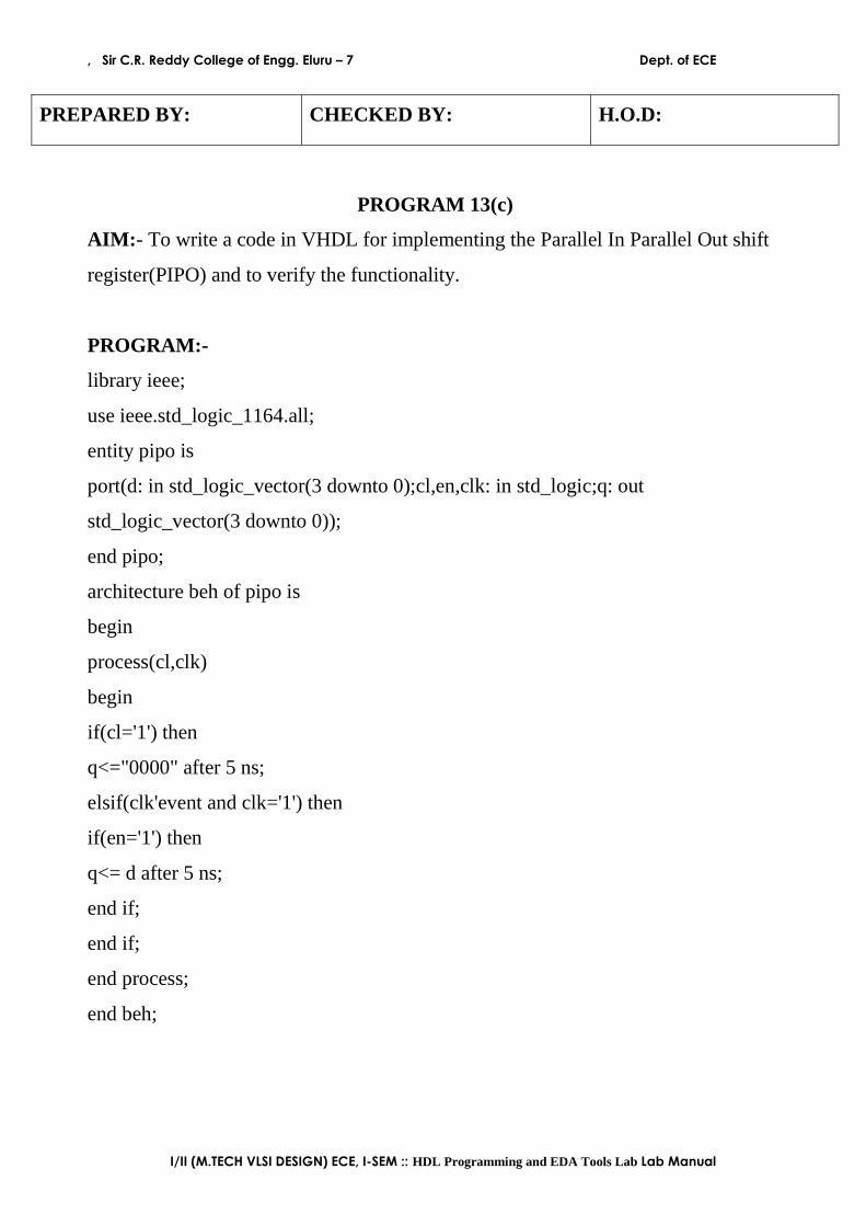
PROGRAM 13(c)
AIM: - To write a code in VHDL for implementing the Parallel In Parallel Out shift
register(PIPO) and to verify the functionality.
PROGRAM:-
library ieee;
use ieee.std_logic_1164.all;
entity pipo is
port(d: in std_logic_vector(3 downto 0);cl,en,clk: in std_logic;q: out
std_logic_vector(3 downto 0));
end pipo;
architecture beh of pipo is
begin
process(cl,clk)
begin
if(cl='1') then
q<="0000" after 5 ns;
elsif(clk'event and clk='1') then
if(en='1') then
q<= d after 5 ns;
end if;
end if;
end process;
end beh;
PREPARED BY: CHECKED BY: H.O.D:

, Sir C.R. Reddy College of Engg. Eluru – 7 Dept. of ECE
I/II (M.TECH VLSI DESIGN) ECE, I-SEM :: HDL Programming and EDA Tools Lab Lab Manual
RTL SCHEMATIC:
WAVEFORMS:
PIPO
, Sir C.R. Reddy College of Engg. Eluru – 7 Dept. of ECE
I/II (M.TECH VLSI DESIGN) ECE, I-SEM :: HDL Programming and EDA Tools Lab Lab Manual
RESULT:- Hence the Parallel In Parallel Out shift register(PIPO) is implemented in
VHDL and the functionality is verified.
PROGRAM-14
PREPARED BY: CHECKED BY: H.O.D:

, Sir C.R. Reddy College of Engg. Eluru – 7 Dept. of ECE
I/II (M.TECH VLSI DESIGN) ECE, I-SEM :: HDL Programming and EDA Tools Lab Lab Manual
PROGRAM 14(a)
AIM: - To write a code in VHDL for implementing the Mealy machine(to detect the
sequence 10) and to verify the functionality.
PROGRAM:-
library ieee;
use ieee.std_logic_1164.all;
entity mealy is
port(a,clk: in std_logic;z: out std_logic);
end mealy;
architecture beh of mealy is
type state is(s0,s1);
signal p_state,n_state: state;
begin
sm: process(clk)
begin
if rising_edge(clk) then
p_state<=n_state;
end if;
end process sm;
cm: process(p_state,a)
begin
case p_state is
when s0=> if(a='0') then z<='0';
n_state<=p_state;

, Sir C.R. Reddy College of Engg. Eluru – 7 Dept. of ECE
I/II (M.TECH VLSI DESIGN) ECE, I-SEM :: HDL Programming and EDA Tools Lab Lab Manual
else z<='0';n_state<=s1;
end if;
when s1=> if(a='1') then z<='0';
n_state<=p_state;
else z<='1';n_state<=s0;
end if;
when others=>z<='0';
n_state<=s0;
end case;
end process cm;
end beh;
STATE TABLE:-
RTL SCHEMATIC:
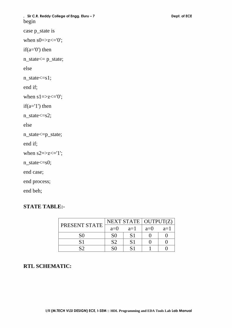
PRESENT STATE NEXT STATE OUTPUT(Z) a=0 a=1 a=0 a=1
S0 S0 S1 0 0 S1 S0 S1 0
MEALY

, Sir C.R. Reddy College of Engg. Eluru – 7 Dept. of ECE
I/II (M.TECH VLSI DESIGN) ECE, I-SEM :: HDL Programming and EDA Tools Lab Lab Manual
WAVEFORMS:
RESULT:- Hence the Mealy machine(to detect the sequence 10) is implemented in
VHDL and the functionality is verified.
, Sir C.R. Reddy College of Engg. Eluru – 7 Dept. of ECE
I/II (M.TECH VLSI DESIGN) ECE, I-SEM :: HDL Programming and EDA Tools Lab Lab Manual
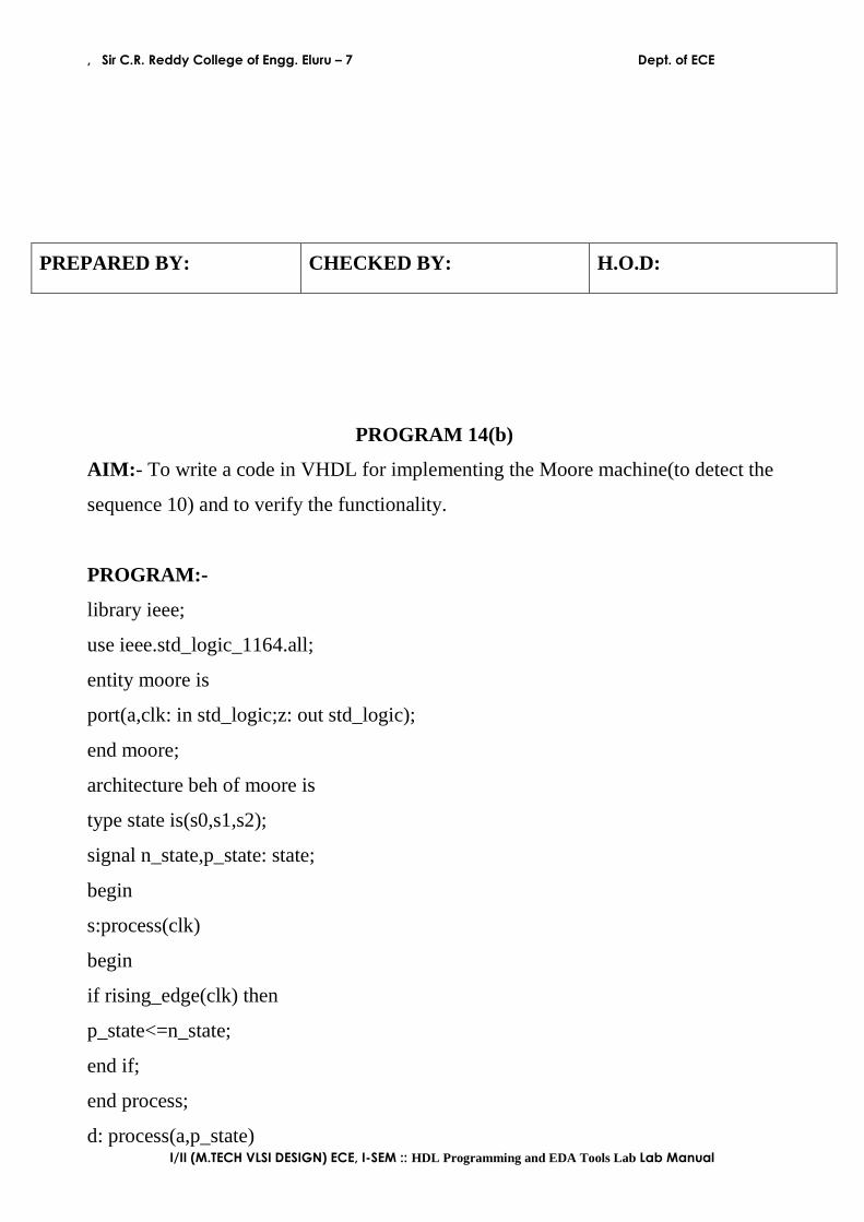
PROGRAM 14(b)
AIM: - To write a code in VHDL for implementing the Moore machine(to detect the
sequence 10) and to verify the functionality.
PROGRAM:-
library ieee;
use ieee.std_logic_1164.all;
entity moore is
port(a,clk: in std_logic;z: out std_logic);
end moore;
architecture beh of moore is
type state is(s0,s1,s2);
signal n_state,p_state: state;
begin
s:process(clk)
begin
if rising_edge(clk) then
p_state<=n_state;
end if;
end process;
d: process(a,p_state)
PREPARED BY: CHECKED BY: H.O.D:
, Sir C.R. Reddy College of Engg. Eluru – 7 Dept. of ECE
I/II (M.TECH VLSI DESIGN) ECE, I-SEM :: HDL Programming and EDA Tools Lab Lab Manual
begin
case p_state is
when s0=>z<='0';
if(a='0') then
n_state<= p_state;
else
n_state<=s1;
end if;
when s1=>z<='0';
if(a='1') then
n_state<=s2;
else
n_state<=p_state;
end if;
when s2=>z<='1';
n_state<=s0;
end case;
end process;
end beh;
STATE TABLE:-
RTL SCHEMATIC:
PRESENT STATE NEXT STATE OUTPUT(Z)
a=0 a=1 a=0 a=1 S0 S0 S1 0 0 S1 S2 S1 0 0 S2 S0 S1 1 0

, Sir C.R. Reddy College of Engg. Eluru – 7 Dept. of ECE
I/II (M.TECH VLSI DESIGN) ECE, I-SEM :: HDL Programming and EDA Tools Lab Lab Manual
WAVEFORMS:
MOORE

, Sir C.R. Reddy College of Engg. Eluru – 7 Dept. of ECE
I/II (M.TECH VLSI DESIGN) ECE, I-SEM :: HDL Programming and EDA Tools Lab Lab Manual
RESULT:- Hence the Moore machine(to detect the sequence 10) is implemented in
VHDL and the functionality is verified.
PREPARED BY: CHECKED BY: H.O.D:

, Sir C.R. Reddy College of Engg. Eluru – 7 Dept. of ECE
I/II (M.TECH VLSI DESIGN) ECE, I-SEM :: HDL Programming and EDA Tools Lab Lab Manual
PROGRAM 14(c)
AIM: - To write a code in VHDL for implementing the Sequence Detector(that
produces an output 1 whenever the sequence 0101 is detected) and to observe the
waveforms.
PROGRAM:-
library ieee;
use ieee.std_logic_1164.all;
entity seqdet is
port(a,clk: in std_logic;z: out std_logic);
end seqdet;
architecture beh of seqdet is
type state is(s0,s1,s2,s3);
signal p_state,n_state: state;
begin
c: process(clk)
begin
if rising_edge(clk) then
p_state<=n_state;
end if;
end process c;
d: process(p_state,a)
begin
case p_state is
when s0=> if(a='0') then z<='0';
n_state<=s1;
else z<='0';n_state<=p_state;
end if;
when s1=> if(a='1') then z<='0';
n_state<=s2;

, Sir C.R. Reddy College of Engg. Eluru – 7 Dept. of ECE
I/II (M.TECH VLSI DESIGN) ECE, I-SEM :: HDL Programming and EDA Tools Lab Lab Manual
else z<='0';n_state<=p_state;
end if;
when s2=> if(a='0') then z<='0';
n_state<=s3;
else z<='0';n_state<=s0;
end if;
when s3=> if(a='1') then z<='1';
n_state<=s2;
else z<='0';n_state<=s1;
end if;
when others=> null;
end case;
end process d;
end beh;
STATE TABLE:-
RTL SCHEMATIC:
PRESENT STATE NEXT STATE OUTPUT(Z) a=0 a=1 a=0 a=1
S0 S1 S0 0 0 S1 S2 S2 0 0 S2 S3 S0 0 0 S3 S1 S2 0 1
SEQDET

, Sir C.R. Reddy College of Engg. Eluru – 7 Dept. of ECE
I/II (M.TECH VLSI DESIGN) ECE, I-SEM :: HDL Programming and EDA Tools Lab Lab Manual
WAVEFORMS:
RESULT:- Hence the Sequence Detector(that produces an output 1 whenever the
sequence 0101 is detected) is implemented in VHDL and the functionality is
verified.
, Sir C.R. Reddy College of Engg. Eluru – 7 Dept. of ECE
I/II (M.TECH VLSI DESIGN) ECE, I-SEM :: HDL Programming and EDA Tools Lab Lab Manual
PROGRAM-15
PREPARED BY: CHECKED BY: H.O.D:

, Sir C.R. Reddy College of Engg. Eluru – 7 Dept. of ECE
I/II (M.TECH VLSI DESIGN) ECE, I-SEM :: HDL Programming and EDA Tools Lab Lab Manual
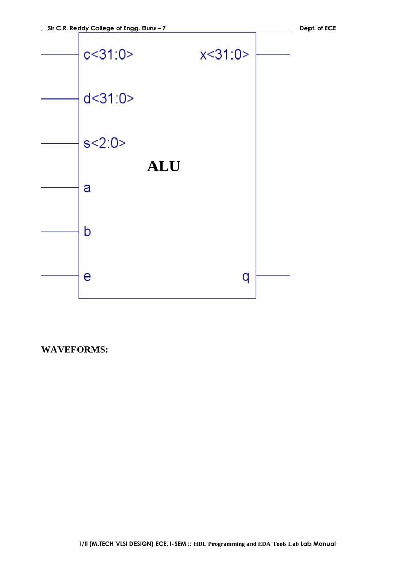
PROGRAM-15
AIM: - To write a code in VHDL for implementing the Arithmetic Logic Unit(ALU)
and to verify the functionality.
PROGRAM:-
library ieee;
use ieee.std_logic_1164.all;
use ieee.std_logic_arith.all;
use ieee.std_logic_unsigned.all;
entity alu is
port(a,b,e: in std_logic;c,d: in integer;s: in std_logic_vector(2 downto 0);q: out
std_logic;x:out integer);
end alu;
architecture alu1 of alu is
begin
process(e,a,b,c,d,s)
begin
if(e='0')then case s is
when"000"=>q<= a or b;
when"001"=>q<= a and b;
when"010"=>q<= not a;
when"011"=>q<= a xor b;
when"100"=>q<= a nand b;
when"101"=>q<= a nor b;
when"110"=>q<= not(a xor b);

, Sir C.R. Reddy College of Engg. Eluru – 7 Dept. of ECE
I/II (M.TECH VLSI DESIGN) ECE, I-SEM :: HDL Programming and EDA Tools Lab Lab Manual
when"111"=>q<= not b;
when others=> null;
end case;
elsif(e='1')then case s is
when"000"=>x<= c+d;
when"001"=>x<= c-d;
when"010"=>x<= c*d;
when"011"=>x<= abs(c);
when"100"=>x<= (c*d)+1;
when"101"=>x<= (c*d)-1;
when"110"=>x<= c+d+1;
when"111"=>x<= c-d-1;
when others=> null;
end case;
end if;
end process;
end alu1;
RTL SCHEMATIC:
, Sir C.R. Reddy College of Engg. Eluru – 7 Dept. of ECE
I/II (M.TECH VLSI DESIGN) ECE, I-SEM :: HDL Programming and EDA Tools Lab Lab Manual
WAVEFORMS:
ALU

, Sir C.R. Reddy College of Engg. Eluru – 7 Dept. of ECE
I/II (M.TECH VLSI DESIGN) ECE, I-SEM :: HDL Programming and EDA Tools Lab Lab Manual
RESULT:- Hence the Arithmetic Logic Unit(ALU) is implemented in VHDL and
the functionality is verified.
PREPARED BY: CHECKED BY: H.O.D:

, Sir C.R. Reddy College of Engg. Eluru – 7 Dept. of ECE
I/II (M.TECH VLSI DESIGN) ECE, I-SEM :: HDL Programming and EDA Tools Lab Lab Manual
PROGRAM-16

, Sir C.R. Reddy College of Engg. Eluru – 7 Dept. of ECE
I/II (M.TECH VLSI DESIGN) ECE, I-SEM :: HDL Programming and EDA Tools Lab Lab Manual
PROGRAM-16
AIM: - To write a code in VHDL for implementing the Clock generator and to verify
the functionality.
PROGRAM:-
library ieee;
use ieee.std_logic_1164.all;
entity test is
port(clk: out std_logic);
end test;
architecture cl of test is
signal t: std_logic:='1';
begin
t<= not t after 5 ns;
clk<= t;
end cl;
RTL SCHEMATIC:

, Sir C.R. Reddy College of Engg. Eluru – 7 Dept. of ECE
I/II (M.TECH VLSI DESIGN) ECE, I-SEM :: HDL Programming and EDA Tools Lab Lab Manual
WAVEFORMS:
RESULT:- Hence the Clock generator is implemented in VHDL and the
functionality is verified.
PREPARED BY: CHECKED BY: H.O.D:

, Sir C.R. Reddy College of Engg. Eluru – 7 Dept. of ECE
I/II (M.TECH VLSI DESIGN) ECE, I-SEM :: HDL Programming and EDA Tools Lab Lab Manual
VHDL VIVA QUESTIONS
1. What is VHDL?
2. What is the need of VHDL?
3. What is meant by simulation?
4. What is meant by synthesis?
5. Who initialized the VHDL and in which year?
6. What is the alternative language for digital systems (other than VHDL)?
7. Explain about top down and bottom up approaches?
8. Explain about VLSI design flow?
9. What is ASIC?
10. Name the different tools that are used to simulate logic designs? Presently
which software are you using and what is its version? Presently which version
is available in market?
11. What is the relationship between VLSI and VHDL?
12. Name the synthesis tool you are using? What is the version? What is the
advanced version of the tool?
13. Mention the library name and package name in VHDL?
14. Is VHDL language a case sensitive or case insensitive language?
15. What is the symbol for ending a line in VHDL?
16. How can you write a comment line in VHDL?
17. What is the difference between signal and variable?
18. How can you declare interfacing signals in entity? Give the syntax?
19. How can you initiate the digital design in VHDL?
20. Explain about the array declarations in VHDL?
21. Difference between bit and std_logic? Does 1076 package support std_logic
type signals?

, Sir C.R. Reddy College of Engg. Eluru – 7 Dept. of ECE
I/II (M.TECH VLSI DESIGN) ECE, I-SEM :: HDL Programming and EDA Tools Lab Lab Manual
22. How can you explain the internal structure of the design in VHDL, give the
syntax?
23. What is behavioral modeling?
24. What is structural modeling?
25. What is dataflow modeling?
26. What is meant by concurrency?
27. What is meant by sequential process?
28. Is dataflow modeling a sequential or concurrent process?
29. Structural modeling is both sequential and concurrent process. Is it true!
30. How can you differentiate behavioral modeling with other modeling?
31. What is meant by sensitivity list?
32. Give different conditional statements in VHDL with their syntaxes?
33. What is meant by component instantiation?
34. How can you declare temporary signals in structural modeling?
35. Mention the different packages in VHDL?
36. VHDL is a 9 valued logic. Is it true? If yes then what are those 9 values?
37. What are the different port declarations?
38. Explain about for loop in VHDL?
39. Give the signal assignment and variable assignment?
40. What is meant by association list and actuals where we can use association
list?
41. What is the use of port map?
42. How can you declare “constants” in VHDL?
43. What is the use of configuration declaration? Explain with a simple example?
44. What is the difference between flip-flop and latch?
45. What is the difference between synchronous and asynchronous processes?
46. Give the syntax for positive edge and negative edge triggered clocks?
47. Give the syntax for nested if?
48. What are different simulations in IC technology?

, Sir C.R. Reddy College of Engg. Eluru – 7 Dept. of ECE
I/II (M.TECH VLSI DESIGN) ECE, I-SEM :: HDL Programming and EDA Tools Lab Lab Manual
49. Explain “Y” chart?
50. What is the need of CPLD and EPGA?
51. What is meant by full custom and semi custom designs?
52. Give the different operators in VHDL?
53. Explain the time delays in VHDL?
54. What is meant by floor planning?
55. What is meant by place and route?
56. What is meant by net list?
57. Is it possible to force clock input to bit type signals. How can you overcome
this problem?