hexagon application kit - infineon technologies
TRANSCRIPT
Microcontrol ler
Hexagon Appl icat ion Ki t For XMC4000 Family
Board User‘s Manual
Revision 1.0, 2013-02-19
CPU_42A-V1 CPU Board XMC4200 Actuator

Edition 2013-02-19
Published by Infineon Technologies AG 81726 Munich, Germany
© 2013 Infineon Technologies AG All Rights Reserved.
Legal Disclaimer
The information given in this document shall in no event be regarded as a guarantee of conditions or characteristics. With respect to any examples or hints given herein, any typical values stated herein and/or any information regarding the application of the device, Infineon Technologies hereby disclaims any and all warranties and liabilities of any kind, including without limitation, warranties of non-infringement of intellectual property rights of any third party.
Information
For further information on technology, delivery terms and conditions and prices, please contact the nearest Infineon Technologies Office (www.infineon.com).
Warnings
Due to technical requirements, components may contain dangerous substances. For information on the types in question, please contact the nearest Infineon Technologies Office.
Infineon Technologies components may be used in life-support devices or systems only with the express written approval of Infineon Technologies, if a failure of such components can reasonably be expected to cause the failure of that life-support device or system or to affect the safety or effectiveness of that device or system. Life support devices or systems are intended to be implanted in the human body or to support and/or maintain and sustain and/or protect human life. If they fail, it is reasonable to assume that the health of the user or other persons may be endangered.

CPU_42A-V1 CPU Board XMC4200 Actuator
Template: IFX_Template_2011-02-24.dot
Revision History
Page or Item Subjects (major changes since previous revision)
Revision 1.0,
2013-02-19
Initial release
Trademarks of Infineon Technologies AG
AURIX™, C166™, CanPAK™, CIPOS™, CIPURSE™, EconoPACK™, CoolMOS™, CoolSET™, CORECONTROL™, CROSSAVE™, DAVE™, EasyPIM™, EconoBRIDGE™, EconoDUAL™, EconoPIM™, EiceDRIVER™, eupec™, FCOS™, HITFET™, HybridPACK™, I²RF™, ISOFACE™, IsoPACK™, MIPAQ™, ModSTACK™, my-d™, NovalithIC™, OptiMOS™, ORIGA™, PRIMARION™, PrimePACK™, PrimeSTACK™, PRO-SIL™, PROFET™, RASIC™, ReverSave™, SatRIC™, SIEGET™, SINDRION™, SIPMOS™, SmartLEWIS™, SOLID FLASH™, TEMPFET™, thinQ!™, TRENCHSTOP™, TriCore™.
Other Trademarks
Advance Design System™ (ADS) of Agilent Technologies, AMBA™, ARM™, MULTI-ICE™, KEIL™, PRIMECELL™, REALVIEW™, THUMB™, µVision™ of ARM Limited, UK. AUTOSAR™ is licensed by AUTOSAR development partnership. Bluetooth™ of Bluetooth SIG Inc. CAT-iq™ of DECT Forum. COLOSSUS™, FirstGPS™ of Trimble Navigation Ltd. EMV™ of EMVCo, LLC (Visa Holdings Inc.). EPCOS™ of Epcos AG. FLEXGO™ of Microsoft Corporation. FlexRay™ is licensed by FlexRay Consortium. HYPERTERMINAL™ of Hilgraeve Incorporated. IEC™ of Commission Electrotechnique Internationale. IrDA™ of Infrared Data Association Corporation. ISO™ of INTERNATIONAL ORGANIZATION FOR STANDARDIZATION. MATLAB™ of MathWorks, Inc. MAXIM™ of Maxim Integrated Products, Inc. MICROTEC™, NUCLEUS™ of Mentor Graphics Corporation. Mifare™ of NXP. MIPI™ of MIPI Alliance, Inc. MIPS™ of MIPS Technologies, Inc., USA. muRata™ of MURATA MANUFACTURING CO., MICROWAVE OFFICE™ (MWO) of Applied Wave Research Inc., OmniVision™ of OmniVision Technologies, Inc. Openwave™ Openwave Systems Inc. RED HAT™ Red Hat, Inc. RFMD™ RF Micro Devices, Inc. SIRIUS™ of Sirius Satellite Radio Inc. SOLARIS™ of Sun Microsystems, Inc. SPANSION™ of Spansion LLC Ltd. Symbian™ of Symbian Software Limited. TAIYO YUDEN™ of Taiyo Yuden Co. TEAKLITE™ of CEVA, Inc. TEKTRONIX™ of Tektronix Inc. TOKO™ of TOKO KABUSHIKI KAISHA TA. UNIX™ of X/Open Company Limited. VERILOG™, PALLADIUM™ of Cadence Design Systems, Inc. VLYNQ™ of Texas Instruments Incorporated. VXWORKS™, WIND RIVER™ of WIND RIVER SYSTEMS, INC. ZETEX™ of Diodes Zetex Limited.
Last Trademarks Update 2011-02-24

CPU_42A-V1 CPU Board XMC4200 Actuator
Table of Contents
Board User's Manual 4 Revision 1.0, 2013-02-19
Table of Contents
Introduction ............................................................................................................................................................ 7
1 Overview ............................................................................................................................................. 7 1.1 Key Features ........................................................................................................................................ 7 1.2 Block Diagram ...................................................................................................................................... 8
2 Hardware Description ........................................................................................................................ 9 2.1 Power Supply ....................................................................................................................................... 9 2.2 Encoder Jumper ................................................................................................................................. 11 2.3 CAN .................................................................................................................................................... 12 2.4 Reset .................................................................................................................................................. 13 2.5 Clock Generation................................................................................................................................ 14 2.6 Boot Option ........................................................................................................................................ 14 2.7 Debug Interface .................................................................................................................................. 15 2.7.1 On-board Debugger ........................................................................................................................... 16 2.7.2 Cortex Debug Connector (10-pin) ...................................................................................................... 17 2.7.3 Cortex Debug+ ETM Connector (20-pin) ........................................................................................... 18 2.8 USB .................................................................................................................................................... 20 2.9 RTC .................................................................................................................................................... 21 2.10 User LEDs and User Button ............................................................................................................... 22 2.11 Potentiometer ..................................................................................................................................... 22 2.12 Satellite Connector ............................................................................................................................. 23 2.12.1 ACT Satellite Connector ..................................................................................................................... 24
3 Production Data................................................................................................................................ 24 3.1 Schematics ......................................................................................................................................... 24 3.2 Component Placement ....................................................................................................................... 29 3.3 Bill of Material (BOM) ......................................................................................................................... 30

CPU_42A-V1 CPU Board XMC4200 Actuator
List of Figures
Board User's Manual 5 Revision 1.0, 2013-02-19
List of Figures
Figure 1 Block Diagram of the CPU Board CPU_42A-V1 .................................................................................. 8 Figure 2 CPU Board XMC4200 Actuator(CPU_42A-V1) ................................................................................... 9 Figure 3 Powering Options ............................................................................................................................... 10 Figure 4 Block Diagram Of Power Supply ........................................................................................................ 10 Figure 5 Encoder Jumper ................................................................................................................................. 11 Figure 6 CAN Interface ..................................................................................................................................... 12 Figure 7 Reset .................................................................................................................................................. 13 Figure 8 Reset LED and Reset Button ............................................................................................................. 13 Figure 9 Clock Generation................................................................................................................................ 14 Figure 10 Boot Options Switch ........................................................................................................................... 14 Figure 11 Installation of Serial Port Driver .......................................................................................................... 16 Figure 12 On-board Debugger ........................................................................................................................... 16 Figure 13 Cortex Debug Connector (10-pin) ...................................................................................................... 17 Figure 14 Cortex Debug Connector (10-pin) Layout .......................................................................................... 17 Figure 15 Cortex Debug+ETM Connector (20-pin) ............................................................................................ 18 Figure 16 Cortex Debug+ ETM Connector (20-pin) Layout ............................................................................... 19 Figure 17 USB Connector .................................................................................................................................. 20 Figure 18 Battery Holder for Coin Cells .............................................................................................................. 21 Figure 19 XMC4200 Power Domains and Real Time Clock .............................................................................. 21 Figure 20 User LED and User Button ................................................................................................................. 22 Figure 21 Satellite Connector ............................................................................................................................. 23 Figure 22 Satellite Connector Type ACT ............................................................................................................ 24 Figure 23 Satellite Connector, USB, CAN .......................................................................................................... 25 Figure 24 XMC4200 ........................................................................................................................................... 26 Figure 25 Power and Debug............................................................................................................................... 27 Figure 26 On-board Debugger ........................................................................................................................... 28 Figure 27 Component Placement ....................................................................................................................... 29

CPU_42A-V1 CPU Board XMC4200 Actuator
List of Figures
Board User's Manual 6 Revision 1.0, 2013-02-19
List of Tables
Table 1 Power status LED’s ............................................................................................................................ 10 Table 2 Power Measurement .......................................................................................................................... 11 Table 3 CAN Connector Pinout (X200) ........................................................................................................... 12 Table 4 Boot Options Settings ........................................................................................................................ 14 Table 5 Cortex Debug Connector (10 Pin) ...................................................................................................... 17 Table 6 Cortex Debug+ ETM Connector (20 Pin) ........................................................................................... 18 Table 7 USB micro AB connector Pinout ........................................................................................................ 20 Table 8 User LEDs .......................................................................................................................................... 22 Table 9 User Buttons ....................................................................................................................................... 22 Table 10 Potentiometer ..................................................................................................................................... 22 Table 11 BOM of CPU_42A-V1-4 Board ........................................................................................................... 30

CPU_42A-V1 CPU Board XMC4200 Actuator
Overview
Board User's Manual 7 Revision 1.0, 2013-02-19
Introduction
This document describes the features and hardware details of the CPU Board XMC4200 Actuator (CPU_42A-V1) designed to work with Infineon’s XMC4200 Microcontroller. This board is part of Infineon’s Hexagon Application Kits.
1 Overview
The CPU board CPU_42A-V1 houses the XMC4200 Microcontroller and the ACT satellite connector for application expansion. The board along with satellite cards (e.g. AUT_ISO-V1, MOT_GPDLV-V2 boards) demonstrates the capabilities of XMC4200. The main use case for this board is to demonstrate motor control and power conversion features of the XMC4200 device including tool chain. The focus is safe operation under evaluation conditions. The board is neither cost nor size optimized and does not serve as a reference design.
1.1 Key Features
The CPU_42A-V1 board is equipped with the following features
XMC4200 (ARM® Cortex™-M4-based) Microcontroller, 256 kByte on-chip Flash, QFN-48
Connection to satellite cards via the ACT satellite connector
USB Device support via micro USB connector
CAN Transceiver with CAN Connector (SUB-D, DE-9 male)
Debug options - On-board Debugger via the Debug USB connector - Cortex Debug connector 10-pin (0.05”) - Cortex Debug+ETM connector 20-pin (0.05”)
Reset push button
Boot from Embedded Flash or CAN
PowerScale Connector: Ready for power consumption analysis
6 LED’s - 3 Power indicating LEDs - 1 User LED (P2.1) - 1 RESET LED - 1 Debug LED
User button connected to P14.7
Potentiometer, connected to analog input P14.4
Power supply - Via Micro-USB connector - Via satellite connector pins (ACT satellite cards can supply power to CPU board) - Via Debug USB connector (Micro USB) - RTC backup battery
CPU_42A-V1 CPU Board XMC4200 Actuator
Overview
Board User's Manual 8 Revision 1.0, 2013-02-19
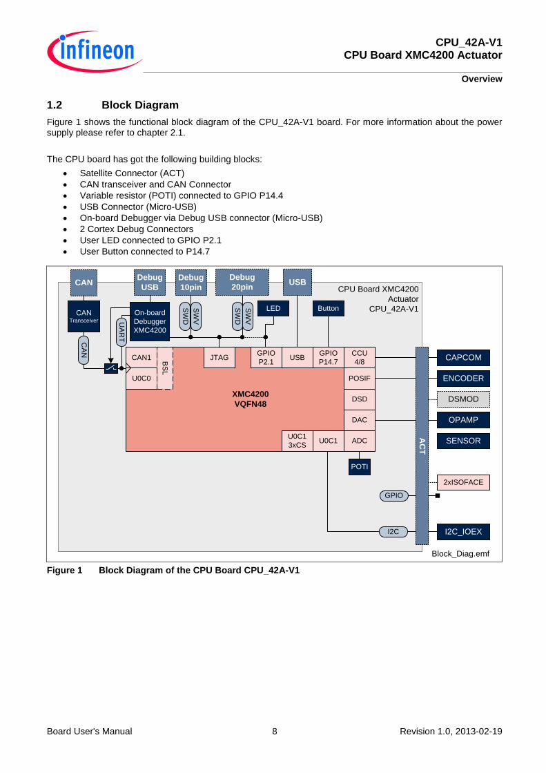
1.2 Block Diagram
Figure 1 shows the functional block diagram of the CPU_42A-V1 board. For more information about the power supply please refer to chapter 2.1.
The CPU board has got the following building blocks:
Satellite Connector (ACT)
CAN transceiver and CAN Connector
Variable resistor (POTI) connected to GPIO P14.4
USB Connector (Micro-USB)
On-board Debugger via Debug USB connector (Micro-USB)
2 Cortex Debug Connectors
User LED connected to GPIO P2.1
User Button connected to P14.7
Figure 1 Block Diagram of the CPU Board CPU_42A-V1
Block_Diag.emf
EE
XMC4200
VQFN48
2xISOFACE
CAPCOM
ENCODER
DSMOD
SENSOR
OPAMP
U0C1
CPU Board XMC4200
Actuator
CPU_42A-V1
USB
USB
POSIF
DSD
DAC
ADC
Debug
20pin
I2C_IOEX
U0C1
3xCS
JTAGS
WV
Debug
10pin
GPIO
P14.7
POTI
I2C
ButtonSW
D
SW
V
CA
N CCU
4/8
GPIO
AC
T
Debug
10pin
Debug
USB
On-board
Debugger
XMC4200
U0C0
CAN1 BS
L
UA
RT
SW
D
LED
GPIO
P2.1
CAN
CAN Transceiver

CPU_42A-V1 CPU Board XMC4200 Actuator
Hardware Description
Board User's Manual 9 Revision 1.0, 2013-02-19
2 Hardware Description
The following sections give a detailed description of the hardware and how it can be used.
Figure 2 CPU Board XMC4200 Actuator(CPU_42A-V1)
2.1 Power Supply
The CPU_42A-V1 board can be powered via either of the USB plugs (5 V); however, there is a current limit that can be drawn from the host PC through USB. If the CPU_42A-V1 board is used to drive other satellite cards e.g. MOT_GPDLV-V2 and the total system current required exceeds 500 mA, then the CPU_42A-V1 board needs to be powered by the satellite cards. These satellite cards support external power supply.
The typical current drawn by the CPU board without any satellite cards connected is about 170 mA (@5 V).
For powering the board through an USB interface, connect the USB cable provided with the kit to either of the Micro-USB connector on board as shown in Figure 3.
Debug
Connectors
Boot
Option
Switch
USB
Connector
Debug USB
Connector
On-board
Debugger
User LED and
User Button
CAN
Connector
CAN
Transciever
ACT
Satellite
Connector
Power
indicating
LEDs
Reset
Circuit
Battery
Holder
Potentiometer Board Interfaces.emf
Encoder
Jumper

CPU_42A-V1 CPU Board XMC4200 Actuator
Hardware Description
Board User's Manual 10 Revision 1.0, 2013-02-19
Figure 3 Powering Options
To indicate the power status of the CPU_42A-V1 board three power indication LED’s are provided on board (see Figure 3). The LED will be “ON” when the corresponding power rail is powered.
Table 1 Power status LED’s
LED Reference Power Rail Voltage Note
V401 VDD5 5 V Must always be “ON”
V402 VDD5USB 5 V “ON” if powered by USB connector X203
“OFF” in all other supply cases
V403 VDD3.3 3.3 V Must always be “ON”
Figure 4 Block Diagram Of Power Supply
Power.emf
USB Debug USB
IFX1763
3.3V linear
LDO Voltage
Regulator
Power
indicating
LEDs
PowerScale
Probe
CPU Board XMC4200 Actuator
CPU_42A-V1
ACT Sat.
Connector
Debug
USB
Lin. Voltage
Regulator
IFX1763
VDDP
U401
JP300U300
Power
LED
VD
D5
VBAT
XMC4200
QFN48
BATTERY
VDD3.3 On Board Devices
VDD3.3
Power_Block.emf
USBPower
LEDPower
LED
VDD5USB +5V VDD5 +5V VDD3.3 +3.3V

CPU_42A-V1 CPU Board XMC4200 Actuator
Hardware Description
Board User's Manual 11 Revision 1.0, 2013-02-19
Hitex PowerScale probe is provided on the CPU_42A-V1 board to measure the power consumption of the XMC4200.
Table 2 Power Measurement
Jumper Function Description
JP300 PowerScale A Hitex PowerScale probe can be connected for current sensing the VDD3.3 (CPU power source). Default: pos. 1-2 (closed)
Note: On the PCB there is a shorting trace between pin 1-2. This trace has to be cut first, before using PowerScale. Pin 3 is GND.
2.2 Encoder Jumper
The jumper JP200 “ENENC#” on the CPU_42A-V1 board is used to enabled/disable an external unit connected to the ACT satellite connector, e.g.an encoder line receiver on the Motor Drive Card MOT_GPLV-V2.
The signal on the encoder jumper is not connected to the XMC4200. It’s connected to pin 30 of the ACT satellite connector only. If the jumper JP200 is shorted, a ground level is driven at pin 30 of the ACT satellite connector. If the jumper is open the line is floating. In this case a pull-up resistor on the ACT satellite card must ensure a high level.
Figure 5 Encoder Jumper
Jumper.emf
Jumper.emf
Encoder
Jumper

CPU_42A-V1 CPU Board XMC4200 Actuator
Hardware Description
Board User's Manual 12 Revision 1.0, 2013-02-19
2.3 CAN
The CPU_42A-V1 board provides a CAN interface via a Sub-D DE-9 connector (X200). Infineon’s high speed CAN transceiver IFX1050GVIO for industrial application supports 3.3V I/O logic and is suitable for 12V and 24V bus systems with an excellent EMC performance. The CAN bus is terminated on-board with 120 Ohm.
Figure 6 CAN Interface
Table 3 shows the signals available at the CAN connector X200.
Table 3 CAN Connector Pinout (X200)
Pin No. Signal Name Description
1 NC No Connection
2 CANL CAN Low
3 GND Ground
4 NC No Connection
5 NC No Connection
6 GND Ground
7 CANH CAN High
8 NC No Connection
9 VDD 5 Volt (not connected, use R201 to apply power to the connector )
The CAN signals CAN_TXD and CAN_RXD are routed to XMC4200 port pins P1.5 and P1.4 respectively via the switches U301 and U303.These switches will disconnect the CAN transceiver from the port pins P1.5 and P1.4 in case a UART function is required. On these pins of the XMC4200 the UART function is overlaid with the CAN function. The UART function can be used for external communication via a USB virtual COM port, which is supported by the on-board debugger.
CPU_42A-V1 CPU Board XMC4200 Actuator
Hardware Description
Board User's Manual 13 Revision 1.0, 2013-02-19
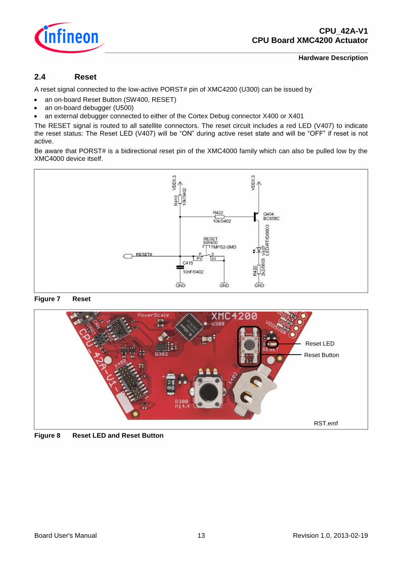
2.4 Reset
A reset signal connected to the low-active PORST# pin of XMC4200 (U300) can be issued by
an on-board Reset Button (SW400, RESET)
an on-board debugger (U500)
an external debugger connected to either of the Cortex Debug connector X400 or X401
The RESET signal is routed to all satellite connectors. The reset circuit includes a red LED (V407) to indicate the reset status: The Reset LED (V407) will be “ON” during active reset state and will be “OFF” if reset is not active.
Be aware that PORST# is a bidirectional reset pin of the XMC4000 family which can also be pulled low by the XMC4000 device itself.
Figure 7 Reset
Figure 8 Reset LED and Reset Button
Reset Button
Reset LED
RST.emf

CPU_42A-V1 CPU Board XMC4200 Actuator
Hardware Description
Board User's Manual 14 Revision 1.0, 2013-02-19
2.5 Clock Generation
An external 12 MHz crystal provides the clock signal to the XMC4200 microcontroller. The drive strength of the oscillator is set to maximum by software, in order to ensure a safe start-up of the oscillator even under worst case conditions. A serial 510 Ohm resistor will attenuate the oscillations during operations.
For the RTC clock a separate external 32.768 kHz crystal is used on board.
Figure 9 Clock Generation
2.6 Boot Option
During power-on-reset the XMC4200 latches the dip switch SW300 settings via the TCK and the TMS pin. Based on the values latched different boot options are possible.
Table 4 Boot Options Settings
BSL (TMS) CAN/UART (TCK) Boot Option
OFF (1) UART (0) Normal Mode (Boot from flash)
ON (0) UART (0) ASC BSL Enabled (Boot from UART)
OFF (1) CAN (1) BMI Customized Boot Enabled
ON (0) CAN (1) CAN BSL Enabled (Boot from CAN)
Figure 10 Boot Options Switch
Boot_Switch.emf
Boot
Option
Switch

CPU_42A-V1 CPU Board XMC4200 Actuator
Hardware Description
Board User's Manual 15 Revision 1.0, 2013-02-19
2.7 Debug Interface
The CPU_42A-V1 board supports debugging via 3 different channels:
On-board debugger
Cortex Debug Connector (10-pin)
Cortex Debug+ETM Connector (20-pin)
The Hexagon Application Boards are designed to use “Serial Wire Debug” as debug interface. JTAG debug is not supported by default because the GPIO P0.7, where the required TDI function is mapped to also, is used by various Actuator boards connected to the ACT satellite connector.
Note: It is strongly recommended not to use JTAG debug mode, especially if satellites boards are connected, which uses the GPIO P0.7. For the same reason also do not use the on-board debugger in JTAG debug mode.
If you want to use the JTAG debug mode through the cortex debug connectors (X400, X401) anyway, enable the JTAG interface of the XMC device by assembling the pull-up resistor R427 (4k7 Ohm) and the resistor R410 (0 - 33 Ohm).

CPU_42A-V1 CPU Board XMC4200 Actuator
Hardware Description
Board User's Manual 16 Revision 1.0, 2013-02-19
2.7.1 On-board Debugger
The on-board debugger [1] supports
Serial Wire Debug
Serial Wire Viewer [2]
Full Duplex UART communication via a USB Virtual COM
[1] Attention: Newer firmware versions of the on-board debugger require the latest J-Link driver (V4.62 or higher) and a Serial Port Driver (CDC driver) installed on your computer. Please check “Install J-Link Serial Port Driver” when installing the latest J-Link driver (see Figure 11)
Figure 11 Installation of Serial Port Driver
[2] If Serial Wire Viewer is used, the User LED cannot freely be programmed and starts flickering, because the Serial Wire Viewer function is overlaid with the GPIO function connected to the User LED.
The on-board debugger can be accessed through the Debug USB connector shown in Figure 12. The Debug LED V502 shows the status during debugging.
Figure 12 On-board Debugger
When using an external debugger connected to the 10pin/20pin Cortex Debug Connector, the on-board debugger is switched off.
When using the USB virtual COM port function of the on-board debugger the on-board CAN interface is disabled through the switches U301 and U303.
Debug.emf
Debug USB
On-board
Debugger
Debug LED

CPU_42A-V1 CPU Board XMC4200 Actuator
Hardware Description
Board User's Manual 17 Revision 1.0, 2013-02-19
2.7.2 Cortex Debug Connector (10-pin)
The CPU_42A-V1 board supports Serial Wire Debug operation and Serial Wire Viewer operation (via the SWO signal when Serial Wire Debug mode is used) through the 10-pin Cortex Debug Connector.
Figure 13 Cortex Debug Connector (10-pin)
Table 5 Cortex Debug Connector (10 Pin)
Pin No. Signal Name Serial Wire Debug JTAG Debug
1 VCC +3.3 V +3.3 V
2 SWDIO / TMS Serial Wire Data I/O Test Mode Select
3 GND Ground Ground
4 SWDCLK / TCK Serial Wire Clock Test Clock
5 GND Ground Ground
6 SWO / TDO Trace Data OUT Test Data OUT
7 KEY KEY KEY
8 NC / TDI Not connected Test Data IN
9 GNDDetect Ground Detect Ground Detect
10 nRESET Reset (Active Low) Reset (Active Low)
Figure 14 Cortex Debug Connector (10-pin) Layout
Cortex Debug
Connector (10-pin)
GNDDetect
SWDIO / TMS
SWDCLK / TCK
1 2
3 4
5 6
7 8
9 10
VCC
GND
GND
KEY
SWO / TDO
NC / TDI
nRESET
cortex-10pin.emf
Cortex Debug
Connector (10 Pin)
10Pin_Conn.emf

CPU_42A-V1 CPU Board XMC4200 Actuator
Hardware Description
Board User's Manual 18 Revision 1.0, 2013-02-19
2.7.3 Cortex Debug+ ETM Connector (20-pin)
The CPU_42A-V1 board supports Serial Wire Debug operation, Serial Wire viewer operation (via SWO connection when Serial Wire Debug mode is used) through the 20-pin Cortex Debug+ ETM Connector. The board does not support the Instruction Trace operation.
JTAG Debug operation additionally would require the TDI (P0.7) signal. By default the TDI signal is disconnected from the Cortex Debug Connectors by a not assembled resistor R410, because the port pin P0.7 is used by the Actuator boards connected to the ACT satellite connector.
Figure 15 Cortex Debug+ETM Connector (20-pin)
Table 6 Cortex Debug+ ETM Connector (20 Pin)
Pin No. Signal Name Serial Wire Debug JTAG Debug
1 VCC +3.3 V +3.3 V
2 SWDIO / TMS Serial Wire Data I/O Test Mode Select
3 GND Ground Ground
4 SWDCLK / TCK Serial Wire Clock Test Clock
5 GND Ground Ground
6 SWO / TDO Trace Data OUT Test Data OUT
7 KEY KEY KEY
8 NC / TDI Not connected Test Data IN
9 GNDDetect Ground Detect Ground Detect
10 nRESET Reset (Active Low) Reset (Active Low)
11 GND/TgtPwr+Cap Ground Ground
12 TRACECLK TRACECLK TRACECLK
13 GND/TgtPwr+Cap Ground Ground
14 TRACEDATA[0]* TRACEDATA[0] TRACEDATA[0]
15 GND Ground Ground
cortex_20pin.emf
SWO / TDO / EXTa / TRACECTL
Cortex Debug+ETM
Connector (20-pin)
GNDDetect
SWDIO / TMS
SWDCLK / TCK
1 2
3 4
5 6
7 8
9 10
VCC
GND
GND
KEY
nRESET
11 12
13 14
15 16
17 18
19 20
NC/EXTb/TDI
TRACECLK(NC)
TRACEDATA[0] (NC)
TRACEDATA[1] (NC)
TRACEDATA[2] (NC)
TRACEDATA[3] (NC)
GND/TgtPwr+Cap
GND/TgtPwr+Cap
GND
GND
GND

CPU_42A-V1 CPU Board XMC4200 Actuator
Hardware Description
Board User's Manual 19 Revision 1.0, 2013-02-19
Table 6 Cortex Debug+ ETM Connector (20 Pin)
Pin No. Signal Name Serial Wire Debug JTAG Debug
16 TRACEDATA[1]* TRACEDATA[1] TRACEDATA[1]
17 GND Ground Ground
18 TRACEDATA[2]* TRACEDATA[2] TRACEDATA[2]
19 GND Ground Ground
20 TRACEDATA[3]* TRACEDATA[3] TRACEDATA[3]
Note: * Not connected on board
Figure 16 Cortex Debug+ ETM Connector (20-pin) Layout
Cortex Debug+ETM
Connector (20 Pin)
20Pin Conn.emf

CPU_42A-V1 CPU Board XMC4200 Actuator
Hardware Description
Board User's Manual 20 Revision 1.0, 2013-02-19
2.8 USB
The XMC4200 supports USB interface in device mode. The power is expected through VBUS (pin 1) from an external host (e.g. PC). When the current consumption of the application running on the Hexagon Application system is higher than 500 mA, power from an external source through satellite cards shall be used.
Note: Some PCs, notebooks or hubs have a weak USB supply which is not sufficient for proper supply. In this case use an external 5 Volt power supply or a powered USB hub.
The VBUS function can be mapped to the HIB_IO_0 pin. A voltage divider (R205/R206) limits the voltage level at the HIB_IO_0 to maximum 3.3V.
Figure 17 USB Connector
Table 7 USB micro AB connector Pinout
Pin No. Pin Name Pin Description
1 VBUS 5 V
2 D- Data Minus
3 D+ Data Plus
4 ID Identification
5 GND Ground

CPU_42A-V1 CPU Board XMC4200 Actuator
Hardware Description
Board User's Manual 21 Revision 1.0, 2013-02-19
2.9 RTC
The XMC4200 CPU has two power domains, the Core Domain and the Hibernate Domain.
The Core Domain (VDDP pins) is connected to the VDD3.3 rail. An on-board LDO voltage regulator generates VDD3.3 (3.3 V) out of VDD5 (5 V).
The Hibernate Domain is powered via the auxiliary supply pin VBAT, which is supplied by either a 3 V coin cell (size 1216, 1220 or 1225) plugged into the battery holder or 3.3 V (VDD3.3) generated by the on-board voltage regulator.
Figure 18 Battery Holder for Coin Cells
The Real Time Clock (RTC) is located in the hibernate domain. Even if the Core Domain is not powered the Hibernate Domain will operate if VBAT is supplied. The RTC keeps running as long as the Hibernate Domain is powered via the auxiliary supply VBAT.
Figure 19 XMC4200 Power Domains and Real Time Clock
Battery.emf
Battery
Holder
Core Domain
CPU
Internal OSC
Hibernate Domain
VBAT
32.768 kHz
XMC4200
VDDPIFX1763
LDO
Voltage Reg.
VDD3.3
+
RTC
SP
I
RTC.emf
Battery
12 MHz
External OSC

CPU_42A-V1 CPU Board XMC4200 Actuator
Hardware Description
Board User's Manual 22 Revision 1.0, 2013-02-19
2.10 User LEDs and User Button
The port pin P2.1 of the XMC4200 is connected to LED V300. More User LED’s are available through the I2C GPIO expander on most of the satellite cards.
Table 8 User LEDs
LED Connected to Port Pin
V300 GPIO P2.1 [1]
[1] If Serial Wire Viewer is used, the User LED at P2.1 is flickering and cannot freely be programmed, because the Serial Wire Viewer function is overlaid with the GPIO function at P2.1.
One User Buttons SW301 is available at GPIO P14.7 of the XMC4200.
Table 9 User Buttons
Button Connected to Pin
BUTTON1 / SW301 GPIO P14.7
Figure 20 User LED and User Button
2.11 Potentiometer
The CPU_42A-V1 board provides a potentiometer POT1 for ease of use and testing of the on-chip analog to digital converter. The potentiometer is connected to the analog input G0_CH4 (P14.4). The analog output voltage of the potentiometer ranges from 0 V to 3.3 V.
Table 10 Potentiometer
Potentiometer Connected to Port Pin
P300 P14.4 / G0_CH4 (Group 0, channel 4)
LED_Button.emf
User Button
User LED

CPU_42A-V1 CPU Board XMC4200 Actuator
Hardware Description
Board User's Manual 23 Revision 1.0, 2013-02-19
2.12 Satellite Connector
The CPU_42A-V1 board provides an ACT (Actuator) satellite connector for application extension by satellite cards.
Note: Satellite cards shall be connected to their matching satellite connectors only. (For e.g. ACT satellite cards shall be connected to ACT satellite connector only)
Figure 21 Satellite Connector
ACT
Satellite
Connector
Sat_Con.emf

CPU_42A-V1 CPU Board XMC4200 Actuator
Production Data
Board User's Manual 24 Revision 1.0, 2013-02-19
2.12.1 ACT Satellite Connector
The ACT satellite connector on the CPU_42A-V1 board allows interface expansion through ACT satellite cards.
XM
C
Pin
VSS
P1
.3
P1
.2
P1
.1
nc
nc
nc
nc
nc
P1
.0
nc
nc
P0
.6
P2
.0
nc
nc
nc
nc
P2
.4
nc
PO
RST
VA
REF
P1
4.8
P1
4.6
nc
nc
P1
4.5
nc
nc
P0
.5
P0
.2
P0
.4
P0
.1
P0
.3
P0
.0
P2
.3
P2
.2
VSS
XM
C F
un
ctio
n
GN
D
PO
SIF0
.IN
0A
/HR
PW
M0
.C0
INB
PO
SIF0
.IN
1A
/HR
PW
M0
.C2
INA
PO
SIF0
.IN
2A
/HW
PW
M0
.C1
INA
nc
nc
nc
nc
nc
CC
U4
0.IN
3A
/HR
PW
M0
.C0
INA
nc
nc
P0
.6
P2
.0/C
CU
40
.IN1
C
2-p
in J
um
per
nc
nc
nc
U0
C1
.SC
LKO
UT
nc
RES
ET#
VA
REF
VA
DC
_G1
CH
0
VA
DC
_G0
CH
6
nc
nc
VA
DC
_G0
CH
5
nc
nc
CC
U8
0.O
UT0
0/H
RO
UT0
0
CC
U8
0.O
UT0
1/H
RO
UT0
1
CC
U8
0.O
UT1
0/H
RO
UT2
1
CC
U8
0.O
UT1
1
CC
U8
0.O
UT2
0/H
RO
UT2
0
CC
U8
0_O
UT2
1
CC
U4
1_O
UT2
CC
U4
1_O
UT3
GN
D
Fun
ctio
n
GN
D
PIF
0IN
1
PIF
0IN
2
PIF
0IN
3
DSD
IN0
DSD
IN1
DSD
IN2
DSD
IN3
RSV
D
CC
_IN
0
CC
_IN
1
CC
_IN
2
ENA
_A
ENA
_B
ENA
_X
SPI_
MTS
R
SPI_
MR
ST
SPI_
SCLK
I2C
_SC
L
GP
IO
RES
ET
VD
D5
VD
D5
AR
EF
DA
C1
/AD
C0
AD
C2
/DA
CR
EF
AD
C4
/OR
C1
AD
C6
/OR
C3
AD
C8
AD
C1
0
AD
C1
2
PW
MA
0_H
PW
MA
0_L
PW
MA
1_H
PW
MA
1_L
PW
MA
2_H
PW
MA
2_L
PW
MX
0
PW
MX
1
GN
D
Satellite 2 4 6 8 10 12 14 16 18 20 22 24 26 28 30 32 34 36 38 40 42 44 46 48 50 52 54 56 58 60 62 64 66 68 70 72 74 76 78 80
Connector 1 3 5 7 9 11 13 15 17 19 21 23 25 27 29 31 33 35 37 39 41 43 45 47 49 51 53 55 57 59 61 63 65 67 69 71 73 75 77 79
Fu
nct
ion
GN
D
PIF
1IN
0
PIF
1IN
1
PIF
1IN
2
PW
MN
PW
MP
DSD
CLK
0
DSD
CLK
1
RSV
D
CC
_IN
3
CC
_IN
4
CC
_IN
5
TRA
P_A
TRA
P_B
TRA
P_X
SPI_
CSA
0
SPI_
CSA
1
SPI_
CSA
2
I2C
_SD
A
AC
T_G
PIO
1
AC
T_G
PIO
0
VD
D5
VD
D5
AG
ND
DA
C0
/AD
C1
AD
C3
/OR
C0
AD
C5
/OR
C2
AD
C7
AD
C9
AD
C1
1
AD
C1
3
PW
MB
0_H
PW
MB
0_L
PW
MB
1_H
PW
MB
1_L
PW
MB
2_H
PW
MB
2_L
PW
MX
2
PW
MX
3
GN
D
XM
C F
un
ctio
n
GN
D
nc
nc
nc
nc
nc
nc
nc
nc
nc
nc
nc
CC
U8
0.IN
0A
nc
nc
nc
nc
nc
U0
C1
.DX
0B
/DO
UT0
nc
nc
AG
ND
VA
DC
_G1
CH
1
nc
VA
DC
_G0
CH
0 (
4)
nc
nc
VA
DC
_G1
CH
3
nc
nc
nc
nc
nc
nc
nc
HR
PW
M0
.HR
OU
T10
HR
PW
M0
.HR
OU
T11
GN
D
XM
C P
in
VSS nc
nc
nc
nc
nc
nc
nc
nc
nc
nc
nc
P0
.7 (
1,6
)
nc
nc
nc
nc
nc
P2
.5
nc
nc
VA
GN
D
P1
4.9
nc
P1
4.0
nc
nc
P1
4.3
nc
nc
nc
nc
nc
nc
nc
P0
.7 (
1)
P0
.8 (
2)
VSS
Pin
ACT
ACT
ACT
CPU_42A-V1
CPU_42A-V1
Figure 22 Satellite Connector Type ACT
(1) P0.7 can also be used for JTAG Debugging (TDI)
(2) P0.8 is used as TRST in order to enable JTAG Debug
(3) This pin is connected with the satellite connector via an analog switch
(4) This ADC input does not support “Out of Range Detection”
(5) This pin must be “enabled” by a solder jump.
(6) Support High Resolution PWM
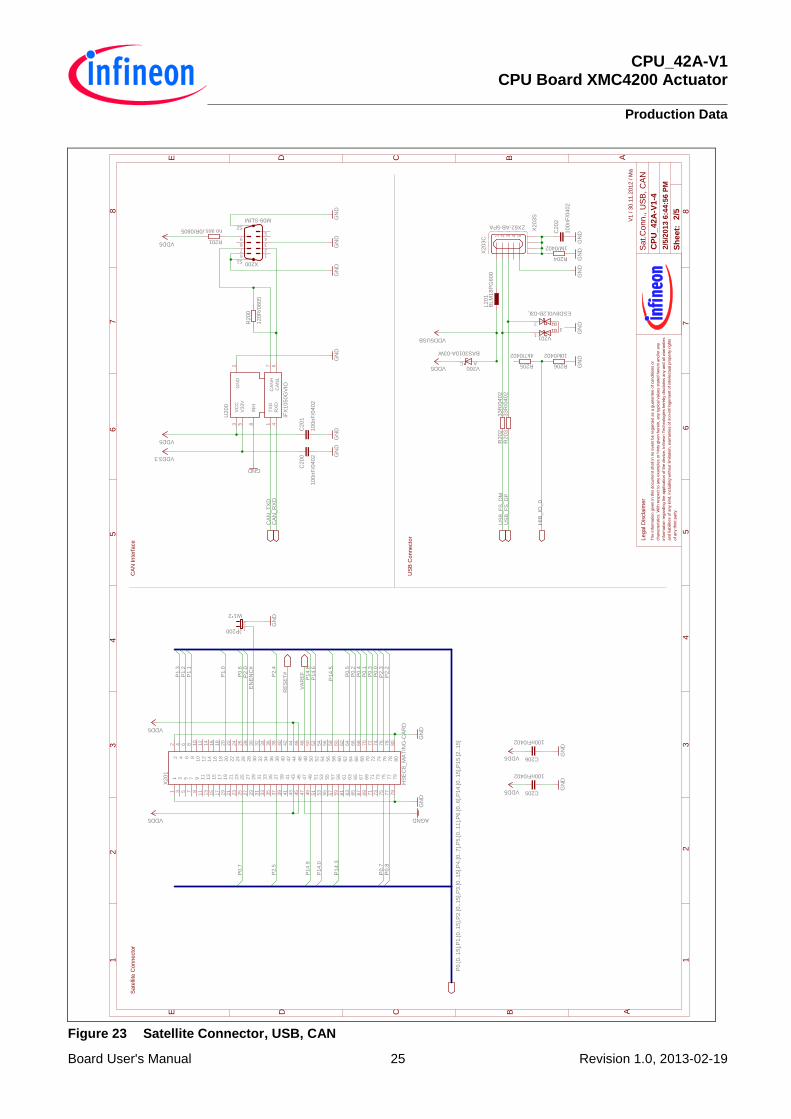
3 Production Data
3.1 Schematics
This chapter contains the schematics for the CPU board:
Satellite Connector, USB, CAN
XMC4200
Power and Debug
On-board Debugger
The board has been designed with Eagle. The full PCB design data of this board can also be downloaded from www.infineon.com/xmc-dev.
CPU_42A-V1 CPU Board XMC4200 Actuator
Production Data
Board User's Manual 25 Revision 1.0, 2013-02-19
Figure 23 Satellite Connector, USB, CAN
AGND
VDD5
100nF
/0402
100nF
/0402
100nF
/0402
100nF/0402
100nF/0402
GN
DG
ND
GN
DG
ND
GN
D
GND
GN
DG
ND
GN
DG
ND
GN
DG
ND
GN
D
GN
D
GN
DG
ND
GN
D
W1*2
BLM
18P
G600
120R
/0805
no ass./0R/0805
33R
/0402
33R
/0402
1M/0402
4k7/0402 10k/0402
VDD5USB
VDD5
VDD5
VDD5
VDD5
VDD3.3
VDD5
VDD5
IFX
1050G
VIO
BAS3010A-03W
ESD8V0L2B-03L
M09-SLIM
HS
EC
8_M
AT
ING
-CA
RD
ZX62-AB-5PA
P0.[0..15],P
1.[0..15],P
2.[0..15],P
3.[0..15],P
4.[0..7],P
5.[0..11],P
6.[0..6],P
14.[0..15],P
15.[2..15]
CA
N_R
XD
CA
N_T
XD
EN
EN
C#
HIB
_IO
_0
P0
.0
P0
.1
P0
.2
P0
.3
P0
.4
P0
.5
P0
.6P
0.7
P0.7
P0.8
P1
.0
P1
.1P
1.2
P1
.3
P2.0
P2.2
P2.3
P2
.4P
2.5
P1
4.0
P14.3
P14.5
P1
4.6
P1
4.8
P1
4.9
RE
SE
T#
US
B_
FS
_D
MU
SB
_F
S_
DP
VA
RE
FC
200
C201
C202
C205
C206
12
JP200L201
R200
R201
R202
R203
R204
R205 R206
CA
NH
7
CA
NL
6
GN
D2
INH
8
RX
D4
TX
D1
V3
3V
5V
CC
3
U200
ACV200
1
23
V201
12345
6789
S1
S2
X200
11
22
33
44
55
66
77
88
99
10
10
11
11
12
12
13
13
14
14
15
15
16
16
17
17
18
18
19
19
20
20
21
21
22
22
23
23
24
24
25
25
26
26
27
27
28
28
29
29
30
30
31
31
32
32
33
33
34
34
35
35
36
36
37
37
38
38
39
39
40
40
41
41
42
42
43
43
44
44
45
45
46
46
47
47
48
48
49
49
50
50
51
51
52
52
53
53
54
54
55
55
56
56
57
57
58
58
59
59
60
60
61
61
62
62
63
63
64
64
65
65
66
66
67
67
68
68
69
69
70
70
71
71
72
72
73
73
74
74
75
75
76
76
77
77
78
78
79
79
80
80
X201
1 2 3 4 5
X203C
X203S
ACT
12
34
56
78
ABCDE
87
65
43
21
E D C B A
CP
U_
42
A-V
1-4
2/5
/20
13
6:4
4:5
6 P
M
2/5
Sh
ee
t:
Legal D
iscla
imer
Th
e in
form
atio
n g
ive
n in
th
is d
ocu
me
nt
sh
all
in n
o e
ve
nt
be
re
ga
rde
d a
s a
gu
ara
nte
e o
f co
nd
itio
ns o
r
ch
ara
cte
ristics.
With
re
sp
ect
to a
ny e
xa
mp
les o
r h
ints
giv
en
he
rein
, a
ny t
yp
ica
l va
lue
s s
tate
d h
ere
in a
nd
/or
an
y
info
rma
tio
n r
eg
ard
ing
th
e a
pp
lica
tio
n o
f th
e d
evic
e,
Infin
eo
n T
ech
no
log
ies h
ere
by d
iscla
ims a
ny a
nd
all
wa
rra
ntie
s
an
d lia
bili
tie
s o
f a
ny k
ind
, in
clu
din
g w
ith
ou
t lim
ita
tio
n,
wa
rra
ntie
s o
f n
on
-in
frin
ge
me
nt
of
inte
llectu
al p
rop
ert
y r
igh
ts
of
an
y t
hird
pa
rty.
D1
D2
US
B C
onnecto
r
Sa
t.C
on
n.,
US
B,
CA
N
V1 / 3
0.1
1.2
012 / M
a
CA
N Inte
rface
Sate
llite
Connecto
r

CPU_42A-V1 CPU Board XMC4200 Actuator
Production Data
Board User's Manual 26 Revision 1.0, 2013-02-19
Figure 24 XMC4200
AGND
AGND
AGND
100nF/0402
100nF/0402
100nF/0402
100nF/0402
100nF/0402
10uF/10V/0805
100nF/0402
100nF/0402
15pF/0402
15pF/0402
15pF/0402
15pF/0402
100nF
/0402
100nF/0402
10uF/10V/0805
10uF/10V/0805
10uF/10V/0805
GN
D
GN
DG
ND
GN
DG
ND
GN
D
GN
DG
ND
GN
DG
ND
GN
D
GN
D
GN
D
GN
DG
ND
GN
DG
ND
BLM18PG600
32.7
68K
Hz
12M
HZ
/S/3
.2X
2.5
POTI/10K/VERT
680R/0603
4k7/0402
4k7/0402
2k2/0603
2k2/0603
10k/0402
510R
/0603
219-0
2
TM
PS
2-S
MD
VDD3.3
VDD3.3
VDD3.3
VDD3.3
VDD3.3
VDD3.3
VDDP
VBAT
VDDP
VDD3.3
XM
C4200_Q
FN
48
74LV
C1G
66D
CK
74LV
C1G
66D
CK
LED-GE/D/0603
P0.[0..15],P1.[0..15],P2.[0..15],P3.[0..15],P4.[0..7],P5.[0..11],P6.[0..6],P14.[0..15],P15.[2..15]
P0.[0..15],P1.[0..15],P2.[0..15],P3.[0..15],P4.[0..7],P5.[0..11],P6.[0..6],P14.[0..15],P15.[2..15]
CA
ND
IS#
CA
N_
RX
D
CA
N_
TX
D
HIB
_IO
_0
P0
.0P
0.1
P0
.2P
0.3
P0
.4P
0.5
P0
.6P
0.7
P0
.8
P1
.0P
1.1
P1
.2P
1.3
P1
.4
P1
.4
P1
.5
P1
.5
P2.0
P2.1
P2
.1
P2.2
P2.3
P2.4
P2
.4
P2.5
P2
.5
P1
4.0
P1
4.3
P1
4.4
P1
4.4
P1
4.5
P1
4.6
P1
4.7
P14.7
P1
4.8
P1
4.9
RE
SE
T#
TC
K
TC
K
TM
S
TM
S
US
B_
FS
_D
MU
SB
_F
S_
DP
VA
RE
F
VD
DC
C300
C302
C303
C304
C306
C308
C310
C311
C312
C315
C316
C317
C318
C322
C323
C325
C326
G
MPJP300
L301
Q301
Q302
AE
SR300
R301
R302
R304
R306
R307
R311
R313
1 234
SW
300
PP
1S S
1
SW
301
EP
AD
EP
AD
HIB
_IO
_0
7
P0
.02
P0
.11
P0
.24
8P
0.3
47
P0
.44
6P
0.5
45
P0
.64
4P
0.7
43
P0
.84
2
P1
.04
0P
1.1
39
P1
.23
8P
1.3
37
P1
.43
6P
1.5
35
P2
.02
6P
2.1
25
P2
.22
4P
2.3
23
P2
.42
2P
2.5
21
P1
4.0
16
P1
4.3
15
P1
4.4
14
P1
4.5
13
P1
4.6
12
P1
4.7
11
P1
4.8
20
P1
4.9
19
PO
RS
T#
32
RT
C_
XT
AL
_1
8
RT
C_
XT
AL
_2
9
TC
K3
4
TM
S3
3
US
B_
D+
4U
SB
_D
-3
VA
GN
D1
7V
AR
EF
18
VB
AT
10
VD
DC
6V
DD
C1
31
VD
DP
5V
DD
P1
28
VD
DP
24
1
VS
S2
7
XT
AL
12
9
XT
AL
23
0
U300
A1
B2
EN
4G
ND
3V
CC
5
U301
A1
B2
EN
4G
ND
3V
CC
5
U303
V300
+
-P
S
1 2
ON
12
34
56
78
ABCDE
87
65
43
21
E D C B A
CP
U_
42
A-V
1-4
2/5
/20
13
6:4
4:5
6 P
M
3/5
Sh
ee
t:
Legal D
iscla
imer
Th
e in
form
atio
n g
ive
n in
th
is d
ocu
me
nt
sh
all
in n
o e
ve
nt
be
re
ga
rde
d a
s a
gu
ara
nte
e o
f co
nd
itio
ns o
r
ch
ara
cte
ristics.
With
re
sp
ect
to a
ny e
xa
mp
les o
r h
ints
giv
en
he
rein
, a
ny t
yp
ica
l va
lue
s s
tate
d h
ere
in a
nd
/or
an
y
info
rma
tio
n r
eg
ard
ing
th
e a
pp
lica
tio
n o
f th
e d
evic
e,
Infin
eo
n T
ech
no
log
ies h
ere
by d
iscla
ims a
ny a
nd
all
wa
rra
ntie
s
an
d lia
bili
tie
s o
f a
ny k
ind
, in
clu
din
g w
ith
ou
t lim
ita
tio
n,
wa
rra
ntie
s o
f n
on
-in
frin
ge
me
nt
of
inte
llectu
al p
rop
ert
y r
igh
ts
of
an
y t
hird
pa
rty.
US
B
Supply
Analo
g
Dig
ital
Hib
ern
ate
/RT
C
CP
UP
ote
ntiom
ete
r, G
PIO
LE
Ds, I2
C P
ullu
ps
Jumper closed with a cutable trace on bottom layer
HitexPowerScale
Boot O
ptions
BS
LO
FF
O
N
UART
CAN
CA
N T
ransceiv
er
Sw
itch
Push B
uttons
CP
U
V1 / 3
0.1
1.2
012 / M
a
LED1
BU
TT
ON
1

CPU_42A-V1 CPU Board XMC4200 Actuator
Production Data
Board User's Manual 27 Revision 1.0, 2013-02-19
Figure 25 Power and Debug
100nF
/0402
100nF
/0402
10uF/10V/0805
10nF/0402 10uF/10V/0805
100nF/0402
100uF
/T/1
0V
/C10nF
/0402
GN
D
GN
D
GN
DG
ND
GN
DG
ND
GN
DG
ND
GN
DG
ND
GN
DG
ND
GN
D
GN
DG
ND
GN
DG
ND
GN
DG
ND
BC
858C
10k/0402
33R
/0402
33R
/0402
33R
/0402
1k5/0603
1k5/0603
680R/0603
no a
ss./33R
/0402
0R
/0603
no ass./0R/0603
10k/0402
2k2/0603
10k/0
402
no a
ss./4k7/0
402
TM
PS
2-S
MD
no ass.
no ass.
no ass.
no ass.
VDD3.3
VDD3.3
VDD5
VDD3.3
VDD3.3
VDD5
VDD3.3
VDD5
VDD3.3
VDD5USB
VDD3.3
VDD3.3
VDD3.3
VBAT
IFX
1763_P
AD
NO
P
LED-GN/D/0603
LED-GN/D/0603
LED-GN/D/0603
BAT54-02V BAT54-02V
BAV70
LED-RT/D/0603
BAS3010A-03W
S2*1
0/1
.27S
O
XE
3K
_D
M2+
CT
X
BK
-885
CA
ND
IS#
DB
GP
RE
S#
DB
GP
RE
S#
P0
.7
P0
.8
P1
.4P
1.5
P2
.1
RE
SE
T#
RE
SE
T#
TC
KT
MS
C400
C401
C405
C406C407
C413
C414
C415
Q404
R401
R402
R403
R404
R405
R406
R407
R410
R416
R417
R419
R420
R422
R427
PP
1S S
1
SW
400
1
TP404
1
TP405
1
TP406
1
TP407BY
P4
EN
5
EX
P9
GN
D3
GN
D6
GN
D7
IN8
OU
T1
SE
NS
E/A
DJ
2
U401
V401
V402
V403
21V404
2 1V405
1
23
V406
V407
ACV408
12
34
56
78
91
01
11
21
31
41
51
61
71
81
92
0
X400
C1
C2
C3
C4
C5
C6
C7
C8
C9
C1
0
D1
D2
D3
D4
D5
D6
X401
1+2+
-
X402
+
12
34
56
78
ABCDE
87
65
43
21
E D C B A
CP
U_
42
A-V
1-4
2/5
/20
13
6:4
4:5
6 P
M
4/5
Sh
ee
t:
Legal D
iscla
imer
Th
e in
form
atio
n g
ive
n in
th
is d
ocu
me
nt
sh
all
in n
o e
ve
nt
be
re
ga
rde
d a
s a
gu
ara
nte
e o
f co
nd
itio
ns o
r
ch
ara
cte
ristics.
With
re
sp
ect
to a
ny e
xa
mp
les o
r h
ints
giv
en
he
rein
, a
ny t
yp
ica
l va
lue
s s
tate
d h
ere
in a
nd
/or
an
y
info
rma
tio
n r
eg
ard
ing
th
e a
pp
lica
tio
n o
f th
e d
evic
e,
Infin
eo
n T
ech
no
log
ies h
ere
by d
iscla
ims a
ny a
nd
all
wa
rra
ntie
s
an
d lia
bili
tie
s o
f a
ny k
ind
, in
clu
din
g w
ith
ou
t lim
ita
tio
n,
wa
rra
ntie
s o
f n
on
-in
frin
ge
me
nt
of
inte
llectu
al p
rop
ert
y r
igh
ts
of
an
y t
hird
pa
rty.
FT
SH
-10
5-0
1-L
-DV
-K
FL
E-1
03
-01
-G-D
V
Cort
ex D
ebug
Debugger
pulls
sig
nal to
GN
D
Ext. d
evic
e p
ulls
sig
nal to
GN
Dand d
isconnects
CA
N s
ignals
from
CA
N T
ransceiv
er
(U200)
VD
D3.3
Supply
RT
C B
attery
Reset
Pow
er
LE
D a
nd T
estp
oin
ts
Po
we
r, D
eb
ug
, R
ese
t
V1 / 3
0.1
1.2
012 / M
a
RE
SE
T
and k
eeps the o
n-b
oard
debugger
in r
eset sta
te
Battery
Hold
er
UA
RT
US
IC0C
H0
CA
NN
od
e1
US
IC_R
xD
US
IC_T
xD
CA
N_T
xD
CA
N_R
xD
P1.4
P1.5
TD
O/S
WO
TD
I
TR
ST

CPU_42A-V1 CPU Board XMC4200 Actuator
Production Data
Board User's Manual 28 Revision 1.0, 2013-02-19
Figure 26 On-board Debugger
15pF/0402
15pF/0402
100nF
/0402
no a
ss./10nF
/0402
100nF/0402
100nF/0402
10uF/10V/0805
100nF/0402
100nF/0402
100nF/0402
10uF/10V/0805
100nF
/0402
GN
DG
ND
GN
DG
ND
GN
D
GN
DG
ND
GN
DG
ND
GN
D
GN
D
GN
D
BLM
18P
G600
12M
HZ
/S/3
.2X
2.5
510R
/0603
33R
/0402
33R
/0402
10k/0402
680R/0603
1M/0402
4k7/0402 10k/0402
VDD3.3
VDD3.3
VDD3.3
VDD5
VDD3.3
XM
C4200_Q
FN
48
ESD8V0L2B-03L
BAS3010A-03W
LED-GN/D/0603
ZX62-AB-5PA
no a
ss.
CA
ND
IS#
CS
CS
DB
GP
RE
S#
DE
BU
G_LE
D#
P0.7
P1.4
P1.5
P2.1
P2.1
RE
SE
T#
TC
K
TC
K
TM
S
VB
US
WT
CK
WT
MS
C500
C501
C502
C503
C504
C505
C506
C507
C508
C509
C510
C511
L500
Q500
R500
R501
R502
R503
R504
R505
R506 R507
EP
AD
EP
AD
HIB
_IO
_0
7
P0
.02
P0
.11
P0
.24
8P
0.3
47
P0
.44
6P
0.5
45
P0
.64
4P
0.7
43
P0
.84
2
P1
.04
0P
1.1
39
P1
.23
8P
1.3
37
P1
.43
6P
1.5
35
P2
.02
6P
2.1
25
P2
.22
4P
2.3
23
P2
.42
2P
2.5
21
P1
4.0
16
P1
4.3
15
P1
4.4
14
P1
4.5
13
P1
4.6
12
P1
4.7
11
P1
4.8
20
P1
4.9
19
PO
RS
T#
32
RT
C_
XT
AL
_1
8
RT
C_
XT
AL
_2
9
TC
K3
4
TM
S3
3
US
B_
D+
4U
SB
_D
-3
VA
GN
D1
7V
AR
EF
18
VB
AT
10
VD
DC
6V
DD
C1
31
VD
DP
5V
DD
P1
28
VD
DP
24
1
VS
S2
7
XT
AL
12
9
XT
AL
23
0
U500
1
23
V500
ACV501
V502
1 2 3 4 5
X500C
X500S
1 2 3 4X501
12
34
56
78
ABCDE
87
65
43
21
E D C B A
CP
U_
42
A-V
1-4
2/5
/20
13
6:4
4:5
6 P
M
5/5
Sh
ee
t:
Legal D
iscla
imer
Th
e in
form
atio
n g
ive
n in
th
is d
ocu
me
nt
sh
all
in n
o e
ve
nt
be
re
ga
rde
d a
s a
gu
ara
nte
e o
f co
nd
itio
ns o
r
ch
ara
cte
ristics.
With
re
sp
ect
to a
ny e
xa
mp
les o
r h
ints
giv
en
he
rein
, a
ny t
yp
ica
l va
lue
s s
tate
d h
ere
in a
nd
/or
an
y
info
rma
tio
n r
eg
ard
ing
th
e a
pp
lica
tio
n o
f th
e d
evic
e,
Infin
eo
n T
ech
no
log
ies h
ere
by d
iscla
ims a
ny a
nd
all
wa
rra
ntie
s
an
d lia
bili
tie
s o
f a
ny k
ind
, in
clu
din
g w
ith
ou
t lim
ita
tio
n,
wa
rra
ntie
s o
f n
on
-in
frin
ge
me
nt
of
inte
llectu
al p
rop
ert
y r
igh
ts
of
an
y t
hird
pa
rty.
US
B
Supply
Analo
g
Dig
ital
Hib
ern
ate
/RT
C
D1
D2
On
-bo
ard
De
bu
gg
er
V1 / 3
0.1
1.2
012 / M
a
On-b
oard
Debugger
Configure
CA
ND
IS# a
s o
pen-d
rain
outp
ut
Configure
debugger-
P0.5
as U
SIC
_T
x b
ut only
active w
hile
X-s
py function is s
ele
cte
dC
onfigure
debugger-
P0.4
as U
SIC
_R
x b
ut only
active w
hile
X-s
py function is s
ele
cte
dC
onfigure
debugger-
P0.3
as R
ES
ET
# d
ete
ct in
put but w
ith a
dditio
nal open-d
rain
outp
ut capabili
ties
SC
LK
OU
T-P
1.1
DX
0B
-P1.4
DX
0D
-P0.0
DO
UT
0-P
2.5
DX
0A
-P2.2
SP
I S
lave
TM
ST
CK
TD
IT
DO
MO
SI
CLK
_O
UT
MIS
O
MIS
O
CS
_IN
CLK
_IN
MO
SI
CS
_O
UT
SP
I M
aste
r
RX
DU
AR
T
U0C
0
U0C
1
U1C
1
DO
UT
0-P
1.5
SE
LO
0-P
1.0
DX
2A
-P2.3
DX
1A
-P2.4
RX
DT
XD
UA
RT
2 (
DM
2)
RX
DT
XD
DX
0A
-P0.4
DO
UT
0-P
0.5
U1C
0
SW
V
Debugger
Concept TX
AC
TIV
E#
GP
IO-P
0.6
EN
#
RE
SE
T#
RE
SE
T#
GP
IO-P
0.3
DE
BU
G_LE
D#
DE
BU
G_LE
D#
GP
IO-P
0.2
TD
O
TD
I
SW
V
TC
K
TM
S

CPU_42A-V1 CPU Board XMC4200 Actuator
Production Data
Board User's Manual 29 Revision 1.0, 2013-02-19
3.2 Component Placement
Figure 27 Component Placement
12
34
+ -
A
PS
GN
D
ON
1
2
P
C
B
E
d
g
e
M09
80
46
44
2
FLEFTSH
ADJ_1
ADJ_2
ADJ_3
C200
C201
C202
C205
C206
C300
C30
2
C303
C304
C306
C308
C310
C311
C31
2
C315
C316
C317
C318
C322
C323
C32
5
C326
C400
C401
C405
C406
C407
C413
C414
C415
C500
C501
C502
C503
C504
C505
C506
C507
C508
C509
C510
C511
JP200
JP
300
L201
L301
L500
Q301
Q302
Q404
Q500
R200
R201
R202
R203R
204
R205R206
R300
R301
R302R304 R306
R307
R311
R313
R401
R402
R403
R404 R405R406
R407
R410
R416
R417
R419
R420R
422
R427
R500
R501R502
R503
R504
R505
R506
R507
SW300
SW301
SW400
TP404
TP405
TP406
TP407
U200
U300
U301U303
U401 U500
V200
V201
V300
V401V402
V403
V404
V405
V406
V407
V408
V500
V501
V502
X200 X201
X203
X400
X401
X402
X500
X501

CPU_42A-V1 CPU Board XMC4200 Actuator
Production Data
Board User's Manual 30 Revision 1.0, 2013-02-19
3.3 Bill of Material (BOM)
Table 11 BOM of CPU_42A-V1-4 Board
Qty Value Device Reference
1 0R/0603 Resistor R416
2 1M/0402 Resistor R204, R505
2 1k5/0603 Resistor R405, R406
3 2k2/0603 Resistor R306, R307, R420
4 4k7/0402 Resistor R205, R302, R304, R506
7 10k/0402 Resistor R206, R311, R401, R419, R422, R503, R507
2 10nF/0402 Capacitor C406, C415
8 10uF/10V/0805 Capacitor, ceramic C308, C323, C325, C326, C405, C407, C506, C510
2 12MHZ/S/3.2X2.5 Crystal, NX3225GD, NDK Q302, Q500
6 15pF/0402 Capacitor C312, C315, C316, C317, C500, C501
1 32.768KHz Crystal, NX3215SA, NDK Q301
7 33R/0402 Resistor R202, R203, R402, R403, R404, R501, R502
2 74LVC1G66DCK IC, Single Analog Switch U301, U303
24 100nF/0402 Capacitor
C200, C201, C202, C205, C206, C300, C302, C303, C304, C306, C310, C311, C318, C322, C400, C401, C413, C502, C504, C505, C507, C508, C509, C511
1 100uF/T/10V/C Capacitor, bipolar C414
1 120R/0805 Resistor R200
1 219-02 Dual DIP-Switch, 0.1" SMD SW300
2 510R/0603 Resistor R313, R500
3 680R/0603 Resistor R301, R407, R504
3 BAS3010A-03W Diode, SOD323, Infineon V200, V408, V501
2 BAT54-02V Diode, SC79, Infineon V404, V405
1 BAV70 Diode, SOT23-3, Infineon V406
1 BC858C Transistor, SOT23-3, Infineon Q404
1 BK-885 Battery Holder, 12mm Coin Cell X402
3 BLM18PG600 Ferrite Bead, 0603, Murata L201, L301, L500
2 ESD8V0L2B-03L Diode, TSLP-3-1, Infineon V201, V500
1 HSEC8_MATING-CARD Connector, Edgecard, Samtec X201
1 IFX1050GVIO IC, CAN Transceiver, Infineon U200
1 IFX1763-3.3 Voltage Regulator, 3.3V LDO, Infineon U401
1 LED-GE/D/0603 LED, yellow V300
4 LED-GN/D/0603 LED, green V401, V402, V403, V502
1 LED-RT/D/0603 LED, red V407
1 DSUB9-male Connector X200
1 POTI/10K/VERT Potentiometer, RK09K1130A8G, ALPS R300
1 S2*10/1.27SO Connector, FTSH-110-01-L-DV-K-P, Samtec X400

CPU_42A-V1 CPU Board XMC4200 Actuator
Production Data
Board User's Manual 31 Revision 1.0, 2013-02-19
2 FSM2JSMA Switch, tactile SW301, SW400
1 W1*2 Pinheader, 2-pin, 0.1” TH JP200
1 XE3K_DM2+CTX
Connector, FTSH-105-01-LM-DV-K, without pin 7, Samtec Connector, FLE-103-01-G-DV, Samtec X401
2 XMC4200_QFN48 IC, XMC4200, QFN48, Infineon U300, U500
2 ZX62-AB-5PA Connector, Micro-USB, Hirose X203, X500
1 no ass. Pinheader, 4-pin, 0.1" TH X501
4 no ass. Pinheader, 1-pin, 0.1" TH TP404, TP405, TP406, TP407
1 no ass./0R/0603 Resistor R417
1 no ass./0R/0805 Resistor R201
1 no ass./4k7/0402 Resistor R427
1 no ass./10nF/0402 Resistor C503
1 no ass./33R/0402 Resistor R410
1 no ass. Pinheader, 3-pin, 0.1" TH, Hitex PowerScale JP300

w w w . i n f i n e o n . c o m
Published by Infineon Technologies AG