high efficiency photovoltaics: on the way to becoming a major electricity source
TRANSCRIPT
Advanced Review
High efficiency photovoltaics: onthe way to becoming a majorelectricity sourceXiaoting Wang,1 John Byrne,1∗ Lado Kurdgelashvili1 andAllen Barnett2
The dramatic growth of the photovoltaic (PV) industry—accelerated by increasedeconomies of scale, technology improvements, research and development efforts,and strong policy support—has pushed PV to set out on its pathway to becoming amajor electricity source. The speed and course of this pathway will be determinedby the development of PV energy price and its relation to market electricity salesprice. The current gap between PV energy price and market electricity sales isoften covered by substantial government subsidies. Using the United States PVmarket as a case study to illustrate the need for PV energy price decline, thisarticle details the potential contribution of high-efficiency PV based on differentmaterials to realize such a decline and a substantial PV electricity share. It isfound that—with considerable government support—PV’s electricity share in theUnited States can rise to 25% by 2050. In order to help the PV industry achievesignificant progress without large government subsidies, more radical declineof PV system cost is necessary. As such, quantitative analysis is deployed toinvestigate the value of module efficiency in lowering the total PV electricity costthrough a levelized cost of energy analysis. Next, the article investigates in detailthe research and development opportunities for high-efficiency PV and projectsthe required efficiency-price ranges for different types of PV modules. C© 2012 JohnWiley & Sons, Ltd.
How to cite this article:WIREs Energy Environ 2012, 1: 132–151 doi: 10.1002/wene.44
INTRODUCTION
H alf a century after the publication of AlbertEinstein’s technical paper explaining the pho-
tovoltaic (PV) effect, the first solar cell that was ca-pable of generating enough power to run everydayelectrical equipment was developed at Bell Labora-tories in 1954.1 By the end of the same century,world PV installations had developed to the order of1 GW capacity.2 During the past decade since 2002,the world cumulative PV capacity has increased from2.26 to 67.4 GW,2,3 with an average annual increaserate of 57.4% for new installations. Assuming annual
∗Correspondence to: [email protected] for Energy and Environmental Policy, University ofDelaware, Newark, DE, USA2School of Photovoltaics and Renewable Energy Engineering, Uni-versity of Delaware, Newark, DE, USA
DOI: 10.1002/wene.44
electricity generation of 1500 kWh per kW PV, 101billion kWh of electricity could have been providedby PV by the end of 2011, a corresponding 0.57% ofthe world electricity consumption in the same year.4
Although still in the early stages of its development,PV has set out on the journey to becoming a seriouselectricity source.
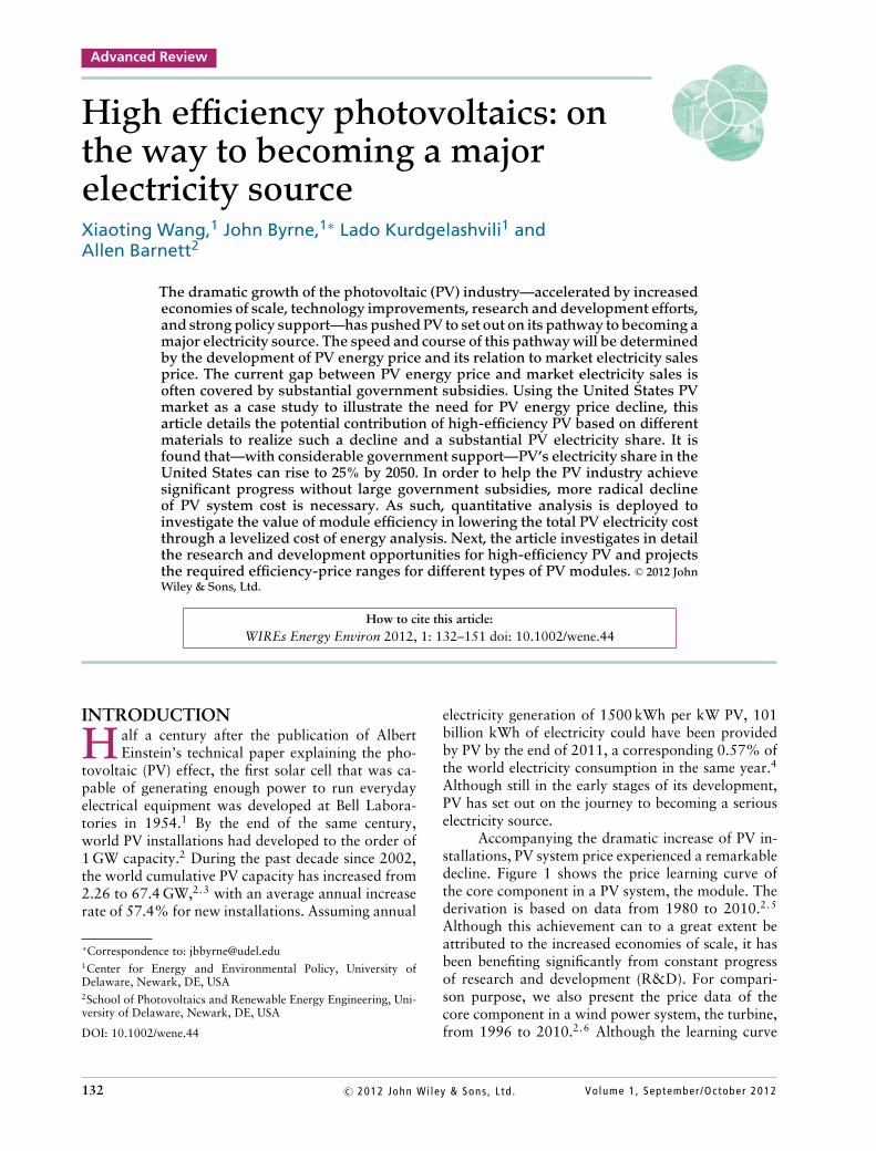
Accompanying the dramatic increase of PV in-stallations, PV system price experienced a remarkabledecline. Figure 1 shows the price learning curve ofthe core component in a PV system, the module. Thederivation is based on data from 1980 to 2010.2,5
Although this achievement can to a great extent beattributed to the increased economies of scale, it hasbeen benefiting significantly from constant progressof research and development (R&D). For compari-son purpose, we also present the price data of thecore component in a wind power system, the turbine,from 1996 to 2010.2,6 Although the learning curve
132 Volume 1, September /October 2012c© 2012 John Wi ley & Sons , L td .
WIREs Energy and Environment High efficiency photovoltaics
y = 1.8731x–0.073
LR=5.0%
y = 6.1282x–0.272
LR=17.2%
0.1
1
10
100
0.01 0.1 1 10 100 1000
Pri
ce (2
000
US
$/W
)
Global cumulative capacity (GW)
Learning curves for PV and wind
PV moduleWind turbine
FIGURE 1 | Price learning curves for PV modules and windturbines. The data on the y-axis for PV modules corresponds to globalaverage price.5 The data on the y-axis for wind turbines corresponds tothe US case that demonstrated a good match with the worldwide caseduring the past 6 years.6
for PV module price is derived based on the normalleast squares (NLSs) method with a good linearityunder logarithmic scales, the learning curve for windturbine price is simply based on the data for 1996 and2010. This is because the learning curve derived withthe NLS method demonstrates an increasing tendencyas cumulative capacity increases due to the divergenceof the price data. PV module price has a learning ratethat is more than three times of that for wind tur-bine price. The great learning ratio for PV moduleprice has greatly benefited from the deeper and widerexploration space, thanks to the rich R&D oppor-tunities at multiple levels, including developments inmaterial, solar cell structure, module structure, fabri-cation equipment, etc.
Currently, there still exists a gap between theprice of PV generated electricity and the market elec-tricity sales price, and this gap is compensated bythe government in the form of subsidy. In this ar-ticle, we use the PV market in the United States asa study case to illustrate the necessity for accelerat-ing PV energy price decline, in order to realize PVas a major electricity source by the middle of thiscentury, without strong dependence on governmentsubsidy.
Because of the need for faster PV energy pricedecline, this article investigates the value of moduleefficiency in lowering the total PV electricity cost.Quantitative analysis is deployed based on the con-cept that a great portion of PV system cost is eitherfixed or related to installation area, and this part ofcost can be reduced when modules of higher efficiencyare adopted, leading to a lower PV energy cost.
Considering the contribution of high module ef-ficiency in lowering PV energy cost, we then focuson R&D opportunities for high efficiency modulesthat are based on solar cells of different materials, in-cluding silicon (Si), Copper Indium Gallium Selenide(CIGS), cadmium telluride (CdTe), Gallium Arsenide(GaAs), and other III–V materials. These opportu-nities cover multiple levels of improvements, rangingfrom material quality, cell and module structures, andconditions that affect module efficiency in long-termoperation.
At the end of this article, we briefly summa-rize the R&D opportunities and project the requiredefficiency–price ranges for different types of PV mod-ules by setting a target PV energy cost of 10 ¢/kWh.Two projections are made based on current nonmod-ule costs and a 30% reduction of these costs. Underthe assumption of a 30% cut on nonmodule costs,flat plate PV modules can be competitive with an ef-ficiency range of 12–26% and the corresponding costrange of 0.9–1.6 $/W. Under the same assumption,concentrating PV modules can be competitive in theefficiency range of 30–40%, with the correspondingcost range of 1.0–1.2 $/W.
PV DIFFUSION IN THE UNITEDSTATES AND GRID PARITYPROJECTION
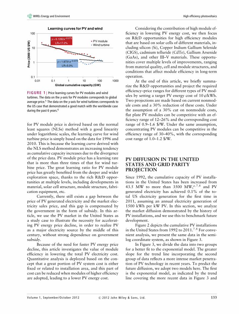
Since 1992, the cumulative capacity of PV installa-tions in the United States has been increased from43.5 MW to more than 3500 MW,a ,7,8 and PVgenerated electricity has achieved 0.1% of the to-tal US electricity generation for the first time in2011, assuming an annual electricity generation of1500 kWh per kW PV. In this section, we analyzethe market diffusion demonstrated by the history ofPV installations, and we use this to benchmark futuredevelopment.
Figure 2 depicts the cumulative PV installationsin the United States from 1992 to 2011.7,8 For conve-nient analysis, we present the same data in the semi-log coordinate system, as shown in Figure 3.
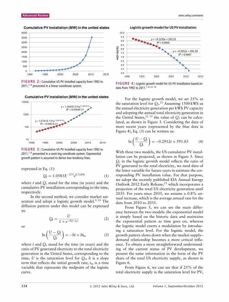
In Figure 3, we divide the data into two groupsfor a better fit to the exponential model. The greaterslope for the trend line incorporating the secondgroup of data reflects a more intense market penetra-tion of PV technology in recent years. To predict thefuture diffusion, we adopt two models here. The firstis the exponential model, as indicated by the trendline covering the more recent data in Figure 3 and
Volume 1, September /October 2012 133c© 2012 John Wi ley & Sons , L td .
Advanced Review wires.wiley.com/wene
0
500
1000
1500
2000
2500
3000
3500
4000
1990 1995 2000 2005 2010 2015
Cumulative PV installation (MW) in the united states
FIGURE 2 | Cumulative US PV installed capacity from 1992 to2011,7,8 presented in a linear coordinate system.
y = 5.9781E-131e 1.5241E-01x
R² = 9.9381E-01
y = 1.0583E-275e 3.1887E-01x
R ² = 9.9396E-01
10
100
1000
10000
Cumulative PV installation (MW) in the united states
FIGURE 3 | Cumulative US PV installed capacity from 1992 to2011,7,8 presented in a semi-log coordinate system. Exponentialgrowth pattern is assumed to derive two tendency lines.
expressed in Eq. (1):
Qt = 1.0583E−275e0.3189t (1)
where t and Qt stand for the time (in years) and thecumulative PV installation corresponding to the time,respectively.
In the second method, we consider market sat-uration and adopt a logistic growth model.9,10 Thediffusion pattern under this model can be expressedas:
Qt = U1 + e−b(t−tm)
(2)
or
ln(
U − Qt
Qt
)= −bt + btm (3)
where t and Qt stand for the time (in years) and theratio of PV generated electricity to the total electricitygeneration in the United States, corresponding to thetime; U is the saturation level for Qt; b is a slopeterm that reflects the initial growth rate; tm is a timevariable that represents the midpoint of the logisticcurve.
y = –0.1225x + 253.22R² = 0.9935
y = –0.2912x + 591.03R² = 0.9947
5.0
5.5
6.0
6.5
7.0
7.5
8.0
8.5
9.0
9.5
10.0
1990 1995 2000 2005 2010 2015
ln[(U
-Qt)/Qt]
Logistic growth model for US PV installation
FIGURE 4 | Logistic growth model for US PV installation based ondata from 1992 to 2011.7,8,12,13
For the logistic growth model, we set 25% asthe saturation level for Qt.11 Assuming 1500 kWh asthe annual electricity generation per kWh PV capacityand adopting the annual total electricity generation inthe United States,12,13 the value of Qt can be calcu-lated, as shown in Figure 3. Considering the data ofmore recent years (represented by the blue dots inFigure 4), Eq. (3) can be written as:
ln(
U − Qt
Qt
)= −0.2912t + 591.03 (4)
With these two models, the US cumulative PV instal-lation can be projected, as shown in Figure 5. SinceQt in the logistic growth model reflects the ratio ofPV generated to the total electricity, we need data ofthe latter variable for future years to estimate the cor-responding PV installation value. For that purpose,we adopt the recently published EIA Annual EnergyOutlook 2012 Early Release,13 which incorporates aprojection of the total US electricity generation until2035. For years since 2035, we assume a 0.8% an-nual increase, which is the average annual rate for thedata from 2010 to 2035.
From Figure 5, we can see the main differ-ence between the two models: the exponential modelis simply based on the historic data and maintainsthe exponential pattern as time goes on, whereasthe logistic model exerts a modulation by introduc-ing a saturation level. For the logistic model, thegrowth pattern slows down when the market supply–demand relationship becomes a more critical influ-ence. To obtain a more straightforward understand-ing of the current status of PV development, wepresent the same information in the form of the PVshare of the total US electricity supply, as shown inFigure 6.
From Figure 6, we can see that if 25% of thetotal electricity supply is the saturation level for PV,
134 Volume 1, September /October 2012c© 2012 John Wi ley & Sons , L td .
WIREs Energy and Environment High efficiency photovoltaics
10
100
1000
10,000
100,000
1,000,000
10,000,000
1980 1990 2000 2010 2020 2030 2040 2050 2060
Cumulative PV installation (MW) in the US: History and Prediction
Exponential prediction
Logistic model prediction
PV history
FIGURE 5 | US PV installation capacity: history and predictionsbased on two models.
0%
5%
10%
15%
20%
25%
30%
1980 1990 2000 2010 2020 2030 2040 2050 2060
Share of PV in electricity supply in the US
Exponential prediction
Logistic model prediction
PV history
FIGURE 6 | US PV electricity share in the total national electricitysupply: history and predictions based on two models.
the current achievement still resides in the ‘innova-tors’ phase.14 Therefore, it is too early to predict anaccurate date of realizing PV as a major electricitysource. However, this projection provides a picturethat shows how close the goal can be if we keepapproaching it with the same amount of effort. Onthe basis of the logistic model, 24.9% of the total USelectricity generation can be supplied by PV in 2049.If the exponential tendency can be maintained in thefollowing decade, during which the two predictionmodels show a good match, approximately 2% shareof electricity can be provided by PV, and this technol-ogy can come to next stage of ‘early adopter’.14
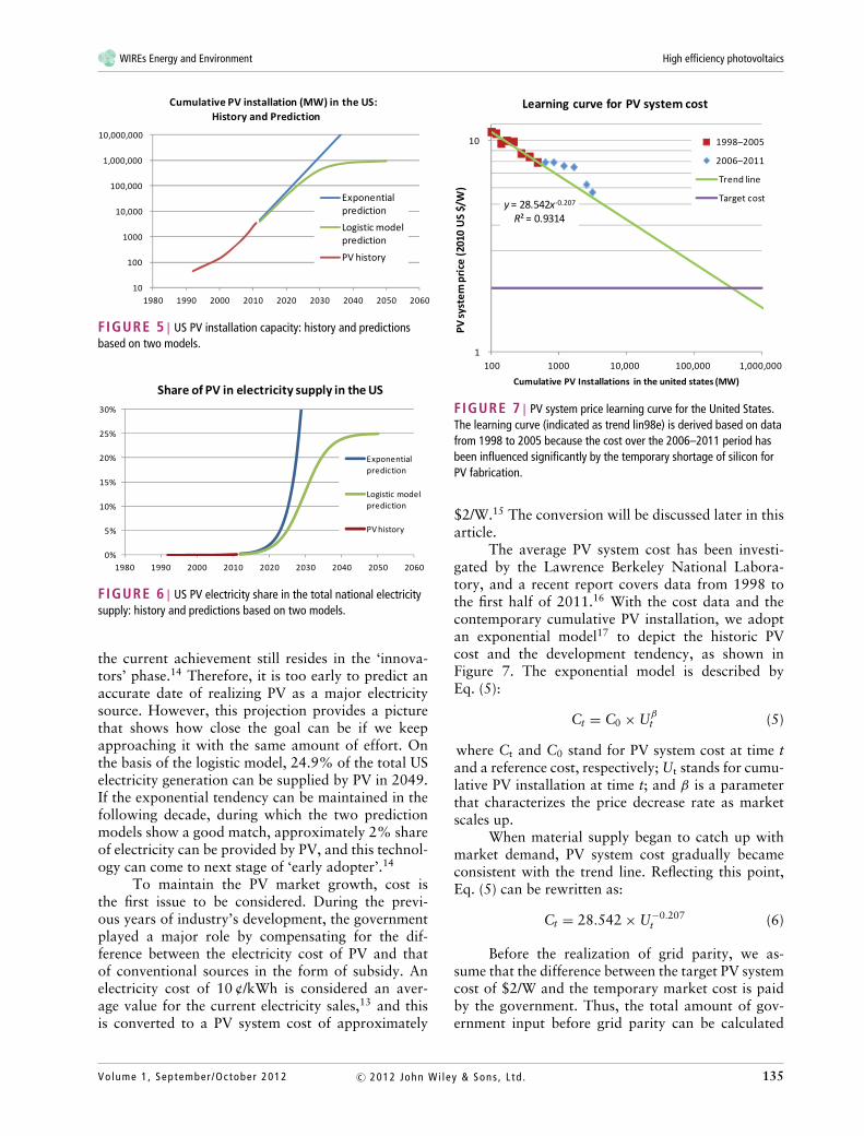
To maintain the PV market growth, cost isthe first issue to be considered. During the previ-ous years of industry’s development, the governmentplayed a major role by compensating for the dif-ference between the electricity cost of PV and thatof conventional sources in the form of subsidy. Anelectricity cost of 10 ¢/kWh is considered an aver-age value for the current electricity sales,13 and thisis converted to a PV system cost of approximately
y = 28.542x-0.207
R² = 0.9314
1
10
100 1000 10,000 100,000 1,000,000
PV sy
stem
pri
ce (2
010
US
$/W
)
Cumulative PV Installations in the united states (MW)
Learning curve for PV system cost
1998–2005
2006–2011
Trend line
Target cost
FIGURE 7 | PV system price learning curve for the United States.The learning curve (indicated as trend lin98e) is derived based on datafrom 1998 to 2005 because the cost over the 2006–2011 period hasbeen influenced significantly by the temporary shortage of silicon forPV fabrication.
$2/W.15 The conversion will be discussed later in thisarticle.
The average PV system cost has been investi-gated by the Lawrence Berkeley National Labora-tory, and a recent report covers data from 1998 tothe first half of 2011.16 With the cost data and thecontemporary cumulative PV installation, we adoptan exponential model17 to depict the historic PVcost and the development tendency, as shown inFigure 7. The exponential model is described byEq. (5):
Ct = C0 × Uβt (5)
where Ct and C0 stand for PV system cost at time tand a reference cost, respectively; Ut stands for cumu-lative PV installation at time t; and β is a parameterthat characterizes the price decrease rate as marketscales up.
When material supply began to catch up withmarket demand, PV system cost gradually becameconsistent with the trend line. Reflecting this point,Eq. (5) can be rewritten as:
Ct = 28.542 × U−0.207t (6)
Before the realization of grid parity, we as-sume that the difference between the target PV systemcost of $2/W and the temporary market cost is paidby the government. Thus, the total amount of gov-ernment input before grid parity can be calculated
Volume 1, September /October 2012 135c© 2012 John Wi ley & Sons , L td .
Advanced Review wires.wiley.com/wene
with Eq. (7):
Ctot =∫ Ug
U0
(28.542 × U−0.207t − Cg)dUt (7)
where Ctot stands for the total investment from thegovernment; U0, Ug, and Ut stand for cumulative PVinstallation at a reference time, the installation goalthat corresponds to grid parity, and installation asa variable, respectively; Cg stands for the PV systemcost goal corresponding to grid parity.
Applying the target PV system cost (Ct) of$2.0/W into Eq. (6), the corresponding target cumula-tive PV installation is calculated to be 369.1 GW, andthis is the value of the variable Ug in Eq. (7). Sincethe most recent cost data corresponds to the first halfof 2011, we consider the cumulative installation atthat time as the starting value (U0) of the integrationin Eq. (7), which is 3.1 GW. Applying these valuesinto Eq. (7), Ctot is calculated to be 178.3 billiondollars.
If the future PV system cost is consistent withthe learning curve as shown in Figure 7 and the elec-tricity cost of conventional sources is maintained, therequired total subsidy from the government is notdependent on the PV installation diffusion pattern.b
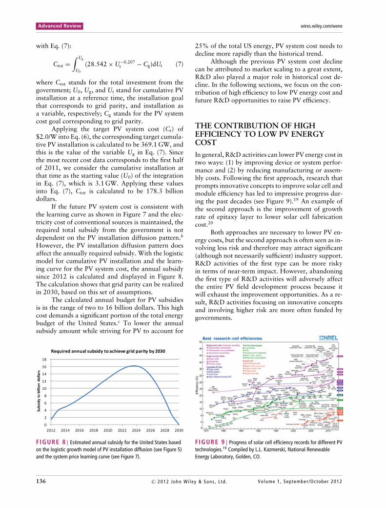
However, the PV installation diffusion pattern doesaffect the annually required subsidy. With the logisticmodel for cumulative PV installation and the learn-ing curve for the PV system cost, the annual subsidysince 2012 is calculated and displayed in Figure 8.The calculation shows that grid parity can be realizedin 2030, based on this set of assumptions.
The calculated annual budget for PV subsidiesis in the range of two to 16 billion dollars. This highcost demands a significant portion of the total energybudget of the United States.c To lower the annualsubsidy amount while striving for PV to account for
0
2
4
6
8
10
12
14
16
18
2012 2014 2016 2018 2020 2022 2024 2026 2028 2030
Subs
idy
in b
illio
n do
llars
Required annual subsidy to achieve grid parity by 2030
FIGURE 8 | Estimated annual subsidy for the United States basedon the logistic growth model of PV installation diffusion (see Figure 5)and the system price learning curve (see Figure 7).
25% of the total US energy, PV system cost needs todecline more rapidly than the historical trend.
Although the previous PV system cost declinecan be attributed to market scaling to a great extent,R&D also played a major role in historical cost de-cline. In the following sections, we focus on the con-tribution of high efficiency to low PV energy cost andfuture R&D opportunities to raise PV efficiency.
THE CONTRIBUTION OF HIGHEFFICIENCY TO LOW PV ENERGYCOST
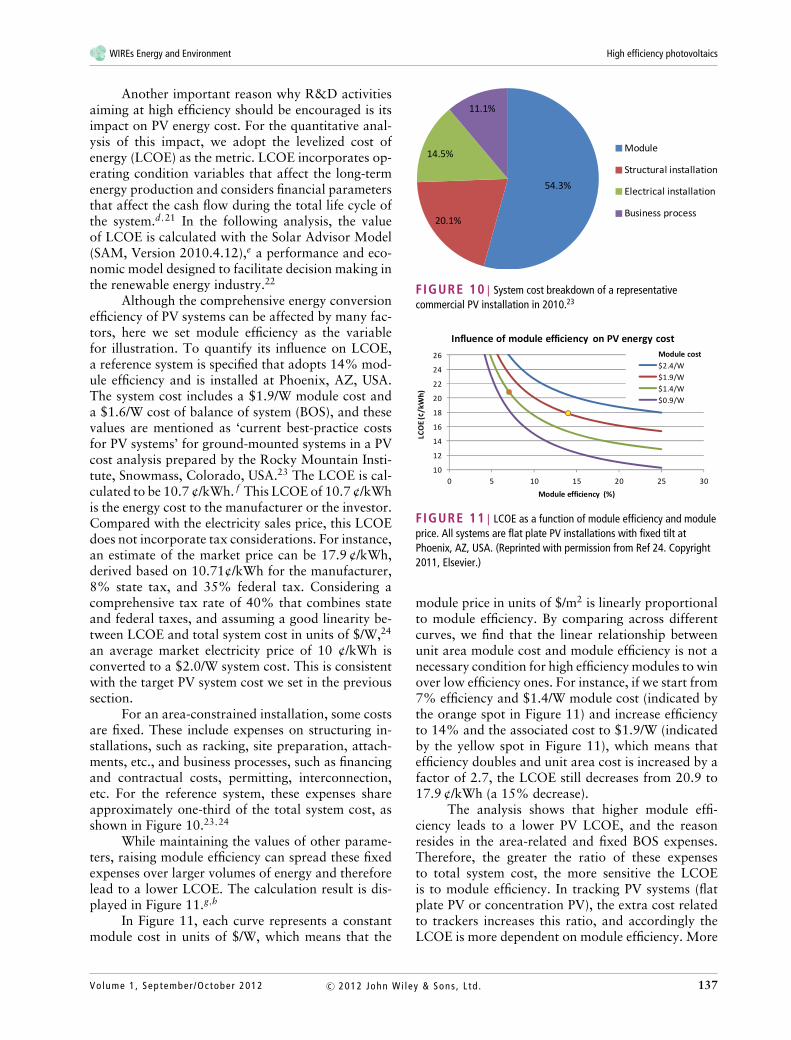
In general, R&D activities can lower PV energy cost intwo ways: (1) by improving device or system perfor-mance and (2) by reducing manufacturing or assem-bly costs. Following the first approach, research thatprompts innovative concepts to improve solar cell andmodule efficiency has led to impressive progress dur-ing the past decades (see Figure 9).19 An example ofthe second approach is the improvement of growthrate of epitaxy layer to lower solar cell fabricationcost.20
Both approaches are necessary to lower PV en-ergy costs, but the second approach is often seen as in-volving less risk and therefore may attract significant(although not necessarily sufficient) industry support.R&D activities of the first type can be more riskyin terms of near-term impact. However, abandoningthe first type of R&D activities will adversely affectthe entire PV field development process because itwill exhaust the improvement opportunities. As a re-sult, R&D activities focusing on innovative conceptsand involving higher risk are more often funded bygovernments.
FIGURE 9 | Progress of solar cell efficiency records for different PVtechnologies.19 Compiled by L.L. Kazmerski, National RenewableEnergy Laboratory, Golden, CO.
136 Volume 1, September /October 2012c© 2012 John Wi ley & Sons , L td .
WIREs Energy and Environment High efficiency photovoltaics
Another important reason why R&D activitiesaiming at high efficiency should be encouraged is itsimpact on PV energy cost. For the quantitative anal-ysis of this impact, we adopt the levelized cost ofenergy (LCOE) as the metric. LCOE incorporates op-erating condition variables that affect the long-termenergy production and considers financial parametersthat affect the cash flow during the total life cycle ofthe system.d,21 In the following analysis, the valueof LCOE is calculated with the Solar Advisor Model(SAM, Version 2010.4.12),e a performance and eco-nomic model designed to facilitate decision making inthe renewable energy industry.22
Although the comprehensive energy conversionefficiency of PV systems can be affected by many fac-tors, here we set module efficiency as the variablefor illustration. To quantify its influence on LCOE,a reference system is specified that adopts 14% mod-ule efficiency and is installed at Phoenix, AZ, USA.The system cost includes a $1.9/W module cost anda $1.6/W cost of balance of system (BOS), and thesevalues are mentioned as ‘current best-practice costsfor PV systems’ for ground-mounted systems in a PVcost analysis prepared by the Rocky Mountain Insti-tute, Snowmass, Colorado, USA.23 The LCOE is cal-culated to be 10.7 ¢/kWh. f This LCOE of 10.7 ¢/kWhis the energy cost to the manufacturer or the investor.Compared with the electricity sales price, this LCOEdoes not incorporate tax considerations. For instance,an estimate of the market price can be 17.9 ¢/kWh,derived based on 10.71¢/kWh for the manufacturer,8% state tax, and 35% federal tax. Considering acomprehensive tax rate of 40% that combines stateand federal taxes, and assuming a good linearity be-tween LCOE and total system cost in units of $/W,24
an average market electricity price of 10 ¢/kWh isconverted to a $2.0/W system cost. This is consistentwith the target PV system cost we set in the previoussection.
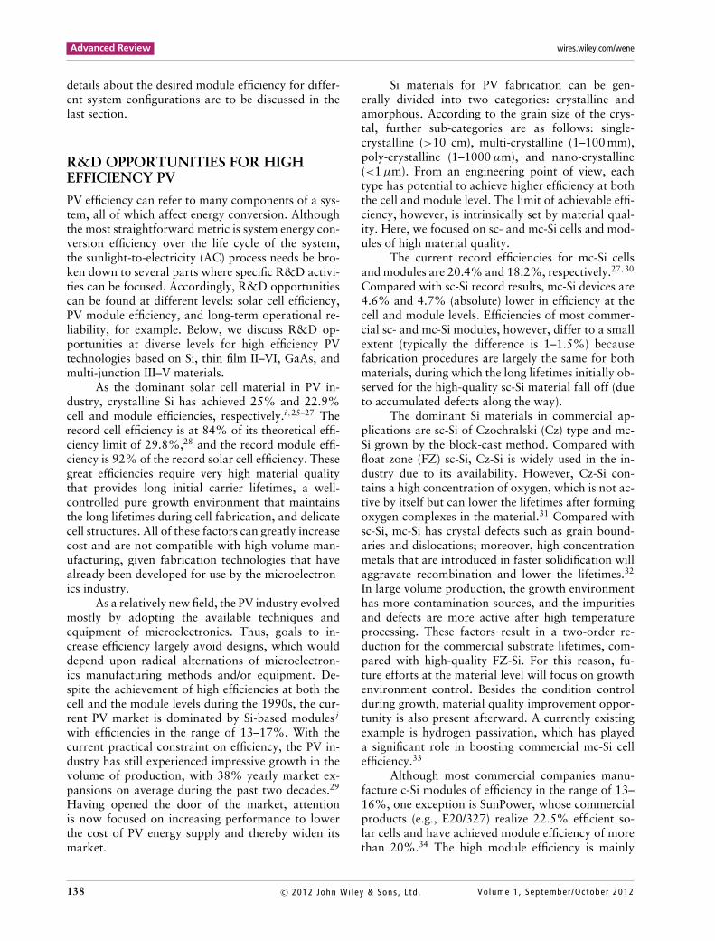
For an area-constrained installation, some costsare fixed. These include expenses on structuring in-stallations, such as racking, site preparation, attach-ments, etc., and business processes, such as financingand contractual costs, permitting, interconnection,etc. For the reference system, these expenses shareapproximately one-third of the total system cost, asshown in Figure 10.23,24
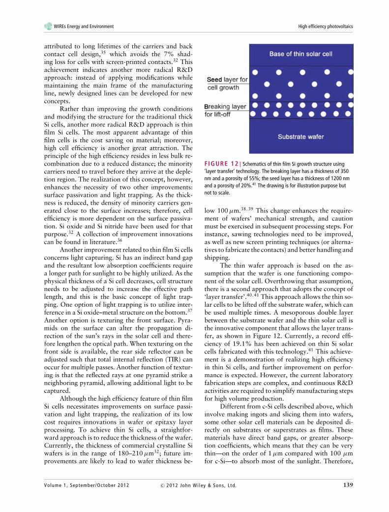
While maintaining the values of other parame-ters, raising module efficiency can spread these fixedexpenses over larger volumes of energy and thereforelead to a lower LCOE. The calculation result is dis-played in Figure 11.g,h
In Figure 11, each curve represents a constantmodule cost in units of $/W, which means that the
54.3%
20.1%
14.5%
11.1%
Module
Structural installation
Electrical installation
Business process
FIGURE 10 | System cost breakdown of a representativecommercial PV installation in 2010.23
10
12
14
16
18
20
22
24
26
0 5 10 15 20 25 30
LCO
E (¢
/kW
h)
Module efficiency (%)
Influence of module efficiency on PV energy costModule cost$2.4/W$1.9/W$1.4/W$0.9/W
FIGURE 11 | LCOE as a function of module efficiency and moduleprice. All systems are flat plate PV installations with fixed tilt atPhoenix, AZ, USA. (Reprinted with permission from Ref 24. Copyright2011, Elsevier.)
module price in units of $/m2 is linearly proportionalto module efficiency. By comparing across differentcurves, we find that the linear relationship betweenunit area module cost and module efficiency is not anecessary condition for high efficiency modules to winover low efficiency ones. For instance, if we start from7% efficiency and $1.4/W module cost (indicated bythe orange spot in Figure 11) and increase efficiencyto 14% and the associated cost to $1.9/W (indicatedby the yellow spot in Figure 11), which means thatefficiency doubles and unit area cost is increased by afactor of 2.7, the LCOE still decreases from 20.9 to17.9 ¢/kWh (a 15% decrease).
The analysis shows that higher module effi-ciency leads to a lower PV LCOE, and the reasonresides in the area-related and fixed BOS expenses.Therefore, the greater the ratio of these expensesto total system cost, the more sensitive the LCOEis to module efficiency. In tracking PV systems (flatplate PV or concentration PV), the extra cost relatedto trackers increases this ratio, and accordingly theLCOE is more dependent on module efficiency. More
Volume 1, September /October 2012 137c© 2012 John Wi ley & Sons , L td .
Advanced Review wires.wiley.com/wene
details about the desired module efficiency for differ-ent system configurations are to be discussed in thelast section.
R&D OPPORTUNITIES FOR HIGHEFFICIENCY PV
PV efficiency can refer to many components of a sys-tem, all of which affect energy conversion. Althoughthe most straightforward metric is system energy con-version efficiency over the life cycle of the system,the sunlight-to-electricity (AC) process needs be bro-ken down to several parts where specific R&D activi-ties can be focused. Accordingly, R&D opportunitiescan be found at different levels: solar cell efficiency,PV module efficiency, and long-term operational re-liability, for example. Below, we discuss R&D op-portunities at diverse levels for high efficiency PVtechnologies based on Si, thin film II–VI, GaAs, andmulti-junction III–V materials.
As the dominant solar cell material in PV in-dustry, crystalline Si has achieved 25% and 22.9%cell and module efficiencies, respectively.i ,25–27 Therecord cell efficiency is at 84% of its theoretical effi-ciency limit of 29.8%,28 and the record module effi-ciency is 92% of the record solar cell efficiency. Thesegreat efficiencies require very high material qualitythat provides long initial carrier lifetimes, a well-controlled pure growth environment that maintainsthe long lifetimes during cell fabrication, and delicatecell structures. All of these factors can greatly increasecost and are not compatible with high volume man-ufacturing, given fabrication technologies that havealready been developed for use by the microelectron-ics industry.
As a relatively new field, the PV industry evolvedmostly by adopting the available techniques andequipment of microelectronics. Thus, goals to in-crease efficiency largely avoid designs, which woulddepend upon radical alternations of microelectron-ics manufacturing methods and/or equipment. De-spite the achievement of high efficiencies at both thecell and the module levels during the 1990s, the cur-rent PV market is dominated by Si-based modules j
with efficiencies in the range of 13–17%. With thecurrent practical constraint on efficiency, the PV in-dustry has still experienced impressive growth in thevolume of production, with 38% yearly market ex-pansions on average during the past two decades.29
Having opened the door of the market, attentionis now focused on increasing performance to lowerthe cost of PV energy supply and thereby widen itsmarket.
Si materials for PV fabrication can be gen-erally divided into two categories: crystalline andamorphous. According to the grain size of the crys-tal, further sub-categories are as follows: single-crystalline (>10 cm), multi-crystalline (1–100 mm),poly-crystalline (1–1000 μm), and nano-crystalline(<1 μm). From an engineering point of view, eachtype has potential to achieve higher efficiency at boththe cell and module level. The limit of achievable effi-ciency, however, is intrinsically set by material qual-ity. Here, we focused on sc- and mc-Si cells and mod-ules of high material quality.
The current record efficiencies for mc-Si cellsand modules are 20.4% and 18.2%, respectively.27,30
Compared with sc-Si record results, mc-Si devices are4.6% and 4.7% (absolute) lower in efficiency at thecell and module levels. Efficiencies of most commer-cial sc- and mc-Si modules, however, differ to a smallextent (typically the difference is 1–1.5%) becausefabrication procedures are largely the same for bothmaterials, during which the long lifetimes initially ob-served for the high-quality sc-Si material fall off (dueto accumulated defects along the way).
The dominant Si materials in commercial ap-plications are sc-Si of Czochralski (Cz) type and mc-Si grown by the block-cast method. Compared withfloat zone (FZ) sc-Si, Cz-Si is widely used in the in-dustry due to its availability. However, Cz-Si con-tains a high concentration of oxygen, which is not ac-tive by itself but can lower the lifetimes after formingoxygen complexes in the material.31 Compared withsc-Si, mc-Si has crystal defects such as grain bound-aries and dislocations; moreover, high concentrationmetals that are introduced in faster solidification willaggravate recombination and lower the lifetimes.32
In large volume production, the growth environmenthas more contamination sources, and the impuritiesand defects are more active after high temperatureprocessing. These factors result in a two-order re-duction for the commercial substrate lifetimes, com-pared with high-quality FZ-Si. For this reason, fu-ture efforts at the material level will focus on growthenvironment control. Besides the condition controlduring growth, material quality improvement oppor-tunity is also present afterward. A currently existingexample is hydrogen passivation, which has playeda significant role in boosting commercial mc-Si cellefficiency.33
Although most commercial companies manu-facture c-Si modules of efficiency in the range of 13–16%, one exception is SunPower, whose commercialproducts (e.g., E20/327) realize 22.5% efficient so-lar cells and have achieved module efficiency of morethan 20%.34 The high module efficiency is mainly
138 Volume 1, September /October 2012c© 2012 John Wi ley & Sons , L td .
WIREs Energy and Environment High efficiency photovoltaics
attributed to long lifetimes of the carriers and backcontact cell design,35 which avoids the 7% shad-ing loss for cells with screen-printed contacts.32 Thisachievement indicates another more radical R&Dapproach: instead of applying modifications whilemaintaining the main frame of the manufacturingline, newly designed lines can be developed for newconcepts.
Rather than improving the growth conditionsand modifying the structure for the traditional thickSi cells, another more radical R&D approach is thinfilm Si cells. The most apparent advantage of thinfilm cells is the cost saving on material; moreover,high cell efficiency is another great attraction. Theprinciple of the high efficiency resides in less bulk re-combination due to a reduced distance; the minoritycarriers need to travel before they arrive at the deple-tion region. The realization of this concept, however,enhances the necessity of two other improvements:surface passivation and light trapping. As the thick-ness is reduced, the density of minority carriers gen-erated close to the surface increases; therefore, cellefficiency is more dependent on the surface passiva-tion. Si oxide and Si nitride have been used for thatpurpose.32 A collection of improvement innovationscan be found in literature.36
Another improvement related to thin film Si cellsconcerns light capturing. Si has an indirect band gapand the resultant low absorption coefficients requirea longer path for sunlight to be highly utilized. As thephysical thickness of a Si cell decreases, cell structureneeds to be adjusted to increase the effective pathlength, and this is the basic concept of light trap-ping. One option of light trapping is to utilize inter-ference in a Si oxide–metal structure on the bottom.37
Another option is texturing the front surface. Pyra-mids on the surface can alter the propagation di-rection of the sun’s rays in the solar cell and there-fore lengthen the optical path. When texturing on thefront side is available, the rear side reflector can beadjusted such that total internal reflection (TIR) canoccur for multiple passes. Another function of textur-ing is that the reflected rays at one pyramid strike aneighboring pyramid, allowing additional light to becaptured.
Although the high efficiency feature of thin filmSi cells necessitates improvements on surface passi-vation and light trapping, the realization of its lowcost requires innovations in wafer or epitaxy layerprocessing. To achieve thin Si cells, a straightfor-ward approach is to reduce the thickness of the wafer.Currently, the thickness of commercial crystalline Siwafers is in the range of 180–210 μm32; future im-provements are likely to lead to wafer thickness be-
FIGURE 12 | Schematics of thin film Si growth structure using’layer transfer’ technology. The breaking layer has a thickness of 350nm and a porosity of 55%; the seed layer has a thickness of 1200 nmand a porosity of 20%.41 The drawing is for illustration purpose butnot to scale.
low 100 μm.38,39 This change enhances the require-ment of wafers’ mechanical strength, and cautionmust be exercised in subsequent processing steps. Forinstance, sawing technologies need to be improved,as well as new screen printing techniques (or alterna-tives to fabricate the contacts) and better handling andshipping.
The thin wafer approach is based on the as-sumption that the wafer is one functioning compo-nent of the solar cell. Overthrowing that assumption,there is a second approach that adopts the concept of‘layer transfer’.40,41 This approach allows the thin so-lar cells to be lifted off the substrate wafer, which canbe used multiple times. A mesoporous double layerbetween the substrate wafer and the thin solar cell isthe innovative component that allows the layer trans-fer, as shown in Figure 12. Currently, a record effi-ciency of 19.1% has been achieved on thin Si solarcells fabricated with this technology.41 This achieve-ment is a demonstration of realizing high efficiencyin thin Si cells, and further improvement on perfor-mance is expected. However, the current laboratoryfabrication steps are complex, and continuous R&Dactivities are required to simplify manufacturing stepsfor high volume production.
Different from c-Si cells described above, whichinvolve making ingots and slicing them into wafers,some other solar cell materials can be deposited di-rectly on substrates or superstrates as films. Thesematerials have direct band gaps, or greater absorp-tion coefficients, which means that they can be verythin—on the order of 1 μm compared with 100 μmfor c-Si—to absorb most of the sunlight. Therefore,
Volume 1, September /October 2012 139c© 2012 John Wi ley & Sons , L td .
Advanced Review wires.wiley.com/wene
solar cells made from these materials are named thinfilm devices. Two thin film devices that have beenextensively explored and have achieved significantprogress are copper–indium–gallium–(di)selenide (ormore simply, CIGS) and CdTe.
With properties that are advantageous for PVapplications, CIGS cells have been researched sincethe early 1970s. This research has led to improvedmaterial deposition methods, better device struc-ture designs, and more cost-effective manufacturingprocedures.42 Here, we only mention the problems tobe solved for the next-generation high efficiency CIGSthin film cells.
The current record efficiencies for CIGS are19.6% and 15.7% at the solar cell and module levels,respectively.27,43 These achievements, however, havebeen partially based on empirical improvements, andthe underlying principles are not yet fully understood.Reproducibility of large volume manufacturing withcurrent achieved performance and further efficiencyimprovement will depend upon a more solid under-standing of the working mechanisms. For instance,it is empirically known that the presence of Na inCIGS is beneficial for PV performance.44 However,the principle underlying the effect of Na has not beenfully understood, although a tentative explanationthat Na helps passivation on grain surface is beinginvestigated.45–48 Another puzzle concerns the influ-ence of grain size on CIGS cell performance. Differentfrom c-Si solar cells, whose performance is directlyrelated to grain size (due to the correlated recombina-tion), CIGS solar cells display insensitivity to grainsize.42 Although tentative explanations are given,the underlying principles are not yet known.50–55 Aswith other solar cells, reducing recombination by im-proving material quality should be a fundamentalR&D direction for CIGS solar cells. For that pur-pose, modeling of the grain boundary behaviors basedon a detailed understanding of the phenomenon isnecessary.
Another R&D focus is to develop a better sub-strate. Because CIGS film growth occurs on top of asubstrate made of a different material, the thermal ex-pansion coefficients of the substrate and the CIGS filmshould be the same in order to avoid stress. A goodmatch of this parameter has been found with soda-lime glass.42 However, this glass begins to soften at500◦C, whereas ideal solar cell fabrication needs anoperating temperature above that point.42 This con-flict does not greatly affect the record cell performancebecause the cell has a small area and its performanceis not very sensitive to glass deformation. However, aglass with higher temperature resistance will be nec-essary for high efficiency large volume production.
Compared with c-Si solar cells, CIGS involvemultiple types of materials in the fabrication. Thisdiversity necessitates more sophisticated control ofmaterial deposition parameters and diagnostic toolsto identify problems. Developing a comprehensivedesign of deposition equipment, manufacturing anddiagnostic tools could greatly improve large volumeproduction, in which reproducibility and uniformityare desired.
A second type of extensively investigated thinfilm solar cells is based on CdTe. The record ef-ficiencies of CdTe are 16.7% and 12.8% at solarcell and module levels, respectively, both of whichare 2.9% (absolute), lower than that for CIGS.27
Notwithstanding its lower efficiency, CdTe experi-enced greater market penetration and developed moremature manufacturing techniques. The biggest CdTecommercial company, First Solar, has achieved a totalmanufacturing capacity of 2.4 GW.55 This companyclaimed that its FS-390 series has a module efficiencyof 12.5%, very close to laboratory record.56
The current CdTe solar cell structure and fabri-cation conditions are based on empirical learning toa great extent, together with a basic understandingof this material. Although the band gap property ofCdTe allows its theoretical solar cell efficiency to beabove 30%, cell efficiency in the laboratory has hov-ered at 16.7% for a decade. The barrier has been com-monly attributed to low open-circuit voltage (Voc) andfill factor (FF). To raise this cell efficiency, a promisingapproach is to improve the quality of the CdS/CdTejunction to achieve lower forward-current recombi-nation. An equally promising direction is to focus onreducing recombination states at the grain boundariesas well as in bulk.57 Besides recombination problems,another challenge is to overcome self-compensationin p-type CdTe doping to achieve the desired dopingconcentration.58,59 Each of these problems requiresbasic research in order to realize a deeper understand-ing of the material’s properties.
Another significant focus for CdTe solar cellsis to stabilize long-term performance. A widely ob-served reliability issue for CdTe solar cells concernsthe barrier at the back contact. Although tentativeexplanations attribute the problem to copper used inthe back contact, a better understanding is needed.60
Besides Si and II–V materials, single-junction so-lar cells have also been researched for and demon-strated by III–V materials, and GaAs stands out withhigh cell efficiency that can be attributed to its directband gap with a value suitable for PV application.However, GaAs solar cells have not been consideredfor wide terrestrial application because the materialis very expensive. This restriction has been recently
140 Volume 1, September /October 2012c© 2012 John Wi ley & Sons , L td .
WIREs Energy and Environment High efficiency photovoltaics
alleviated by the noticeable progress of adopting ‘lift-off’ technology in GaAs cells.61 This lift-off technol-ogy allows the expensive substrate to be re-used afterthe epitaxial film is removed, and therefore the mate-rial cost is greatly reduced. Although not many fabri-cation details have been released by Alta Device, thecommercial company that has deployed R&D on thistopic, the basic concept is considered similar to the‘layer transfer’ for Si thin cells. With this technology,a cell efficiency of 28.3% has been achieved; this isnot only a new record for GaAs cells but also a recordfor all types of single-junction cells.27 Furthermore,the efficiency of the modules made of thin film GaAscells by the same company has created a record of23.5%, which for the first time surpassed the 22.9%single-junction solar module efficiency that had beenmaintained by Si modules.27 The new high cell andmodule efficiencies open another promising avenuefor low cost high efficiency PV in terrestrial appli-cations. Research priorities include: (1) maintainingthe high efficiency of solar cells grown from the samesubstrate; (2) exploring the limit of substrate re-use;(3) raising the growth rate of metal organic chemi-cal vapor deposition (MOCVD) currently being usedfor epitaxial layer growth, or exploring other high-speed growth techniques; (4) producing larger mod-ules of good uniformity; and (5) developing manu-facturing equipment and procedures for high volumeproduction.
Although single-junction solar cells of dif-ferent materials are being improved for higherefficiency, multi-junction solar cells have alsodemonstrated a great progress. III–V materials areextensively explored for this purpose because theyprovide wide options of band gap and lattice constantfor system optimization. Because of the high cost re-lated to expensive materials and complex fabricationsteps, multi-junction solar cells are usually adopted inconcentrating PV (CPV) configurations for terrestrialapplication.
Efforts to incorporate concentrators into PVmodules date back to the 1970s.62 The basic ideais to use low-cost optical concentrators to reduce therequired area of solar cells, which are more expensivethan optics. Using the ratio of a concentrator’s activearea to a solar cell’s area as the standard, CPV canbe categorized as low-X (1–10X), mid-X (10–100X),and high-X (100–1000X).k In this section, we reviewthe current status and potential R&D opportunitiesfor the currently dominant type, high-X CPV.
The most commonly adopted III–V multi-junction solar cells have three sub-cells, and their costis two orders higher than that of Si cells. High-Xconcentrators may therefore be necessary for these
multi-junction solar cells to compete with Si cells.Moreover, high-X CPV depends upon high-accuracytracking, which introduces a significant additionalcost. To compensate for the high costs of both so-lar cells and trackers, the commercial CPV systems inthe market are usually around 500X.
Triple-junction concentration solar cells haveachieved a record efficiency of 43.5% at 418X.27
Applying the principle of detailed balance, an idealtriple solar cell with band gaps of 0.94, 1.34, and1.86eV63 that are optimized for current-match con-ditions can operate with an efficiency of 55.9% atthe same concentration. The realized solar cell effi-ciency corresponds to 78% of the theoretical limit.Researchers continue to investigate even higher cellefficiency by applying alternative growth techniquesto relax the restriction posed by lattice match sothat the band gaps can further approach the theo-retical optimal values. One example is the invertedlattice-mismatched GaInP/GaInAs/GaInAs solar cellthat can tolerate more lattice mismatch by growingthe epitaxial layers inversely and gradually increas-ing the order of lattice mismatch.64,65 This growthtechnique can realize band gaps closer to the the-oretically optimal values and therefore higher solarcell efficiency. Efficiency (40.8%) at 326X has beenachieved,64 and 45% efficiency is expected with con-tinued development.66 Although noticeable progresshas been observed on triple-junction concentrationsolar cells under standard measurement conditions,their performance in long-term operation needs morecareful assessment.
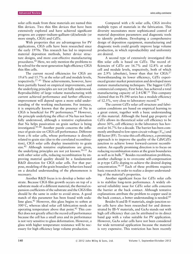
Triple-junction solar cells adopted in commer-cial CPV systems utilize a monolithic structure withthe three sub-cells connected in series. Both the de-sign and measurement of these solar cells are basedon a reference spectrum, usually ASTM G-173-03Direct.67 However, the real spectrum can experiencedynamic variation. The current match among thethree sub-cells, or at least between the top and middlesub-cells, can be achieved under the reference spec-trum, but it cannot be maintained constantly in realoperation. Figure 13 shows the calculated efficien-cies under different spectrum conditions for a triple-junction monolithic solar cell with band gaps opti-mized for current match.
The solar cell efficiencies in Figure 13 are cal-culated for 100X concentration and are based on thedetailed balance model.63,68–70 The purpose of Figure13 is not to show the absolute value of the efficiencybut to demonstrate the large efficiency deviation fora triple-junction monolithic solar cell; this great devi-ation is due to current mismatch caused by spectrumvariation. In Figure 13, the red curve is derived based
Volume 1, September /October 2012 141c© 2012 John Wi ley & Sons , L td .
Advanced Review wires.wiley.com/wene
FIGURE 13 | Calculated efficiencies for ideal two-terminaltriple-junction cells at 100X. The black dots are calculated using realspectrum at Golden, CO, USA in 2002. The red line is calculated undera simple assumption that air mass is the only factor that affectsspectrum.
on the assumption that the spectrum is only affectedby the air mass, and all other parameters that influ-ence the spectrum are constants. The black dots arederived with the available real spectra measured in2002 for Golden CO, every 60 seconds. The vari-ation range can be greater than 20% even at highirradiation ranges. In Figure 13, efficiencies are notplotted in the low irradiation range because spectrumdata are not available under those conditions.71,72
As CPV plays a more serious role in the PV mar-ket, the spectrum sensitivity issue has garnered moreand more attention. Exploring research pertinent tothis topic can be found in recent publications byacademic institutes and commercial companies.73–78
Considering the significant influence of spectrum vari-ation on solar cell efficiency and the limited spectrumdata resources, it would be valuable to deploy moreR&D activities to quantify spectrum sensitivity. Theresearch can indicate the proper locations for CPV in-stallations, where dynamic spectrum variation is ob-served to be comparatively low. For those locationswith relatively stable spectrum conditions, the bandgaps of the three sub-cells may be tuned for optimalenergy generation in long-term operation.
Another focus of CPV research is to further splitthe spectrum, using four, five, or even six junctionsto absorb the broadband spectrum.79 Combining thisstrategy with efforts to adjust band gaps to approachthe optimal values can lead to future solar cell ef-ficiency increases. However, actual operating condi-tions suggest that expanded spectrum splitting may
create more problems than it solves. Highly dynamicspectrum variation raises doubt about the value ofdeveloping four-, five-, or six-junction solar cells, atleast in a monolithic structure for terrestrial applica-tion. Figure 13 shows analyses only for triple-junctionsolar systems because they are the actual structuresbeing adopted in the existing CPV market. It is pre-dictable that, as the divisions of the spectrum increase,the solar cell efficiency will have a higher sensitivityto spectrum variation and therefore will experiencemore energy loss when the spectrum deviates from thestandard. It remains to be seen if the efficiency gainby increasing the number of sub-cells predicted un-der the standard spectrum can be realized in field ap-plications when dynamic spectrum variation occurs.For example, a switch from three to four sub-cellsresults in a theoretical efficiency gain of 8% (rela-tive) under the standard spectrum.63,68,80 However,in the field, a higher sensitivity to spectrum variationmay make the energy production of the four-cell sys-tem close to or even lower than that of the three-cellsystem.
Different from monolithic solar cells which splitthe spectrum in a vertical or a series way, anotherconcept called ‘lateral spectrum splitting’ has recentlybeen applied in some R&D projects.81,82 The basicprinciple is to split the spectrum using additional op-tics before the sunlight arrives at solar cells designedfor different wavelength ranges. With the lateral spec-trum splitting approach, the cells can be fabricatedand optimized separately, and this can completely orpartially release the restrictions of current match orlattice match. 36.7% and 38.5% record submoduleefficiencies have been demonstrated on prototypes ofdifferent structures.83,84 However, to prove the feasi-bility of this concept, more R&D efforts are requiredon the variation design of the electronic circuit be-cause multiple outputs are present in the lateral struc-ture compared with one output in the monolithicstructure; also R&D efforts are required on modulestructure optimization because more components arepresent in the lateral structure than in the monolithicstructure.
Besides spectrum variation, another importantissue that affects the performance of concentrationtriple-junction cells is the nonuniformity of illumina-tion. In both the design and measurement phases ofsuch a solar cell, it is assumed that the illuminationis uniform across its surface. Although this condi-tion is satisfied for flat plate PV, it cannot be guaran-teed when a cell is assembled together with a concen-trator and installed in the field. Although secondaryoptical components in high-X CPV are designed tohomogenize the rays that pass through the primary
142 Volume 1, September /October 2012c© 2012 John Wi ley & Sons , L td .
WIREs Energy and Environment High efficiency photovoltaics
concentrators, the designs are based on perfect track-ing. When a tracking error occurs in field operations,the uniformity found in ideal tracking is not neces-sarily maintained. The nonuniformity of illuminationdirectly causes voltage difference across a solar cell,which leads to lateral current flow and can be re-flected as low FF on the I–V curve. This effect was an-alyzed as early as 1960 on a single p–n junction85 anddiscussed in the 1990s on a monolithic two-junctionsolar cell.86 The influence of nonuniform illuminationon monolithic multi-junction solar cells necessitatesthree-dimensional analysis because the junctions areaffecting each other when connected in series. Recentresearch suggests that in a CPV module utilizing sec-ondary optics, the FF decreases by more than 4%,whereas the short circuit current or Isc decreases byless than 2% at a tracking error of 0.5◦.87 Consid-ering the potential gain by improving the FF in realoperating conditions, more R&D activities can be de-ployed to design secondary optics incorporating dif-ferent tracking errors.
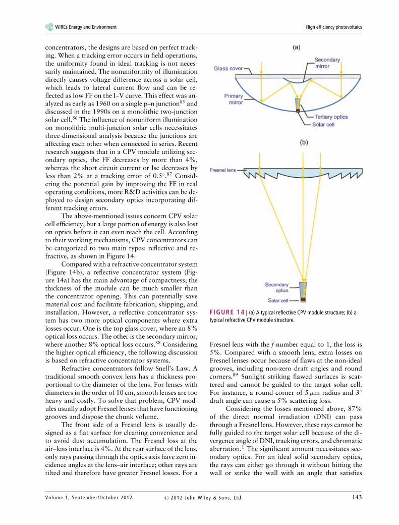
The above-mentioned issues concern CPV solarcell efficiency, but a large portion of energy is also loston optics before it can even reach the cell. Accordingto their working mechanisms, CPV concentrators canbe categorized to two main types: reflective and re-fractive, as shown in Figure 14.
Compared with a refractive concentrator system(Figure 14b), a reflective concentrator system (Fig-ure 14a) has the main advantage of compactness; thethickness of the module can be much smaller thanthe concentrator opening. This can potentially savematerial cost and facilitate fabrication, shipping, andinstallation. However, a reflective concentrator sys-tem has two more optical components where extralosses occur. One is the top glass cover, where an 8%optical loss occurs. The other is the secondary mirror,where another 8% optical loss occurs.88 Consideringthe higher optical efficiency, the following discussionis based on refractive concentrator systems.
Refractive concentrators follow Snell’s Law. Atraditional smooth convex lens has a thickness pro-portional to the diameter of the lens. For lenses withdiameters in the order of 10 cm, smooth lenses are tooheavy and costly. To solve that problem, CPV mod-ules usually adopt Fresnel lenses that have functioninggrooves and dispose the chunk volume.
The front side of a Fresnel lens is usually de-signed as a flat surface for cleaning convenience andto avoid dust accumulation. The Fresnel loss at theair–lens interface is 4%. At the rear surface of the lens,only rays passing through the optics axis have zero in-cidence angles at the lens–air interface; other rays aretilted and therefore have greater Fresnel losses. For a
FIGURE 14 | (a) A typical reflective CPV module structure; (b) atypical refractive CPV module structure.
Fresnel lens with the f-number equal to 1, the loss is5%. Compared with a smooth lens, extra losses onFresnel lenses occur because of flaws at the non-idealgrooves, including non-zero draft angles and roundcorners.89 Sunlight striking flawed surfaces is scat-tered and cannot be guided to the target solar cell.For instance, a round corner of 5 μm radius and 3◦
draft angle can cause a 5% scattering loss.Considering the losses mentioned above, 87%
of the direct normal irradiation (DNI) can passthrough a Fresnel lens. However, these rays cannot befully guided to the target solar cell because of the di-vergence angle of DNI, tracking errors, and chromaticaberration.1 The significant amount necessitates sec-ondary optics. For an ideal solid secondary optics,the rays can either go through it without hitting thewall or strike the wall with an angle that satisfies
Volume 1, September /October 2012 143c© 2012 John Wi ley & Sons , L td .
Advanced Review wires.wiley.com/wene
TIR. Only considering the 4% Fresnel loss at the topsurface and assuming zero absorption in the solid,the comprehensive optical efficiency is 83% at per-fect system pointing.
Although CPV trackers are still under devel-opment for more stable performance under diverseconditions, it is difficult to accurately quantify thefrequency of tracking errors in field operation at thismoment. For an optimistic estimation, we assume 5%efficiency loss due to pointing error, which can causedecline of both FF and Isc of the solar cells.
The sophisticated module structure and the ac-companying high risk make high-X CPV more com-plex than choosing its higher cell efficiency. Startingfrom 40% solar cell efficiency, we can estimate thecomprehensive efficiency based on the above discus-sion. The estimated values for the influencing fac-tors include: (1) a 10% loss due to current mismatchamong sub-cells under dynamic spectrum variation;(2) a 17% optical losses at ideal system pointing;and (3) an extra 5% loss when considering the point-ing errors in long-term operation. These values leadto a 28.4% efficient CPV module. However, this ef-ficiency is based on several assumptions, includingideal secondary optics, well-controlled system point-ing, and spectrum sensitivity derived based on limitedspectrum data. Even this seemingly high module effi-ciency does not guarantee CPV’s superiority over flatplate systems because CPV can only utilize the directbeam and the diffuse light is wasted. Only consider-ing the usable irradiation and the module efficiency,a CPV system using 28.4% efficiency modules gener-ates the same energy as a tracking flat plate systemusing 21.9% efficiency modules of the same activearea, for a location where DNI is 77% of the globalnormal irradiation (GNI). Seventy-seven percent is arepresentative value for the annual DNI–GNI ratio atlots of locations in United States, including Phoenix,Arizona, and Las Vegas.m
For future CPV modules of higher efficiency,there can be two major R&D directions: small unitsand low-mid X concentrations. The small unit con-cept means that each submodule has a small activearea, creating several advantages. The first is at theoptics level. The thickness of a smooth convex lensis proportional to its diameter, so a small dimensionof the submodules of a CPV system allows smoothlenses to be adopted; therefore, the scattering loss atthe non-ideal grooves of Fresnel lenses can be elimi-nated. The second advantage is at the electrical level.As the submodule area decreases, the resistive lossdecreases. This is because the output power from asubmodule is proportional to its operating current,or its active area, whereas its resistive loss is pro-
portional to the square of its operating current. Thethird advantage is at the thermal level. For the sameconcentration, small submodules correspond to smallsolar cells and a smaller dimension of the cells isbeneficial to heat dissipation. This is good becausea cell’s efficiency is inversely proportional to its op-erating temperature. The fourth advantage is at thematerial level. For the same concentration, small sub-modules correspond to thinner modules. Therefore,materials can be saved and lower cost is requiredfor shipping and installation. A commercial companynamed Semprius has adopted this small-unit conceptand applied smooth lenses in the CPV modules. Arecent measurement demonstrated 33.9% efficiencyof the Semprius modules under the standard testingconditions.90
Accompanying the advantages, there are twonew problems. First, for the same active module area,small units mean a greater amount of the units, whichmay increase costs related to assembly. Currently,this problem has been solved by a technology called‘micro-printing’, which is adopted by Semprius.91,92
This technology can process many tiny solar cells atthe same time. The other problem is the increasedsensitivity to alignment error. Misalignment in actualmanufacturing or assembling can cause higher lossesfor small submodules because a certain absolute valueof the misalignment corresponds to a greater fractionof the operation dimension. It is yet to be proventhat the high alignment accuracy can be maintainedin both laboratory conditions and real operation.
Another R&D direction to achieve higher CPVmodule efficiency can be switching from high to low-mid concentration. Lower concentration can elimi-nate the use of secondary optics and/or reduce thesensitivity to system pointing. The success of this vari-ation is intrinsically dependent on the cost decline ofthe multi-junction solar cells.
Current technology used to fabricate III–V so-lar cells is MOCVD and most of the equipmentis made by a commercial company named Veeco.Veeco is developing new growth tools to realize fastgrowth of crystalline layers and reduce the fabrica-tion cost of the solar cells.93 Another explorationdirection is to adopt an innovation concept of ‘lift-off’ that allows multiple uses of expensive substratesfor growth of thin epitaxial layers. Research on thistopic has been mentioned in previous paragraphs forthin Si cells40,41 and thin GaAs cells.61 For multi-junction cells, the micro-printing technology of thesame concept has been adopted by Semprius and itallows the transfer of the tiny cells away from thegrowth substrate, indicating the potential of substratere-use.94
144 Volume 1, September /October 2012c© 2012 John Wi ley & Sons , L td .
WIREs Energy and Environment High efficiency photovoltaics
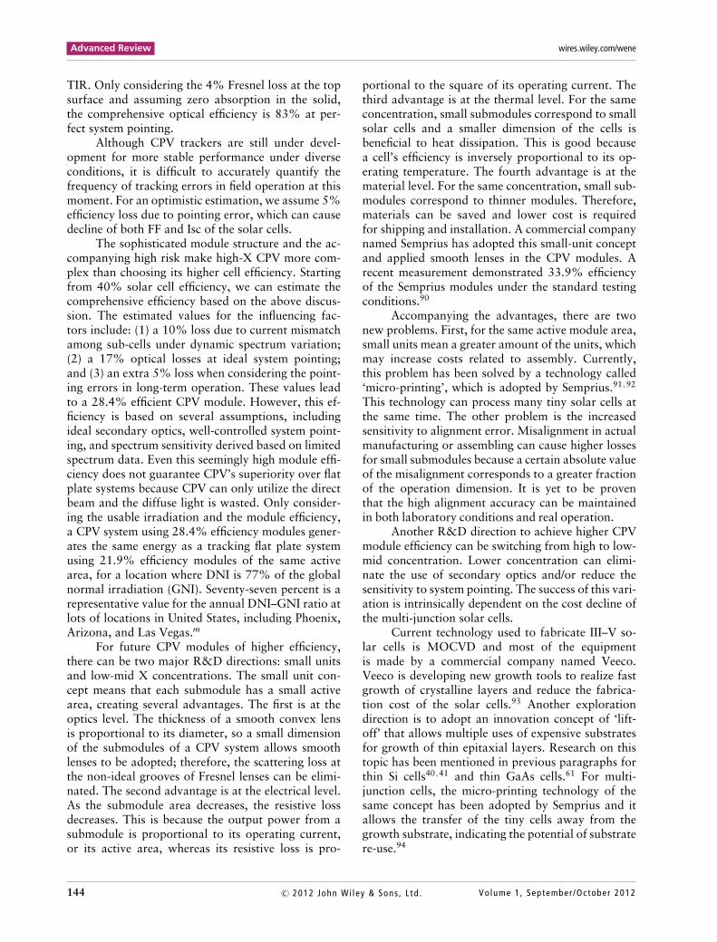
TABLE 1 Absolute Values of Efficiency Achievements for Different PV Technologies
Theoretical cell (η) Laboratory record cell (η) Laboratory record module (η) Market module (η)
sc-Si 29.8%1 25.0% 22.9% 14–17%; 20%2
mc-Si 20.4% 18.2% 12–15%CIGS 31.6% 19.6% 15.7% 11–13%CdTe 30.3% 16.7% 12.8% 11–12%GaAs 31.2% 28.3% 23.5% NA3
Multi-J 55.9%4 43.5% 33.9%5 25–30%
1The limit for Si is based on the detailed balance model but also incorporates the absorption coefficients and carrier lifetimes.28 Thetheoretical limits for other materials are calculated based on detailed balance model and the only considered material parameter is theenergy band gap.2The 20% module efficiency is based on back-contact solar cell structure, so this value is listed separately.3Commercial products were not available at the time of this article.4For comparison purpose, this value is calculated for the same concentration level as the measurement condition for the recordtriple-junction solar cell: 418X AM 1.5 Direct.5This new record was based on tests at the Instituto de Energıa Solar at the University of Madrid, Spain.90 All the other recordefficiencies are cited from the Solar Cell Efficiency Tables being updated in Progress in Photovoltaics: Research and Applications.27
SUMMARY AND DISCUSSION
During the past two decades, the PV industry has ex-perienced dramatic growth, which was triggered bystrong policy support and accelerated by increasedeconomies of scale and technology improvements. Al-though the exponential diffusion pattern brought bythe diverse efforts has pushed PV to set out on thejourney to becoming a major electricity source, it isstill in the innovator phase. With the historic PV in-stallation data and a logistic model, it is predictedthat PV can achieve a 25% electricity share in theUnited States by 2050. To realize this target, numer-ous subsidies are required from the government, if thefuture cost of PV systems starts from the currentlyobserved average value of $5.7/W and follows the13.4% learning rate that is demonstrated by history.In order to help the PV industry achieve sustainableprogress without relying on the large subsidy from thegovernment, more radical decline of PV system costis needed. Although the influence of market scaling isrelatively stable and predictable, we can find more ex-ploration space from the R&D side. In this article, wefocus on R&D opportunities for high efficiency PV,following a quantitative proof of the value of highmodule efficiency in lowering PV energy cost.
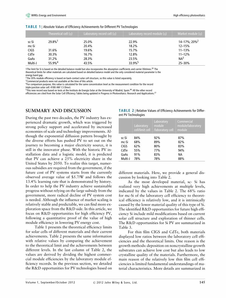
Table 1 presents the theoretical efficiency limitsfor solar cells of different materials and their currentachievements. Table 2 presents the same informationwith relative values by comparing the achievementto the theoretical limit and the achievements betweendifferent levels. In the last column of Table 2, thevalues are derived by dividing the highest commer-cial module efficiencies by the laboratory module ef-ficiency records. In the previous section, we detailedthe R&D opportunities for PV technologies based on
TABLE 2 Relative Values of Efficiency Achievements for Differ-ent PV Technologies
Laboratorycell/limit cell
Laboratorymodule/laboratory cell
Commercialmodule/laboratorymodule
sc-Si 84% 92% 87%mc-Si 68% 89% 82%CIGS 62% 80% 83%CdTe 55% 77% 94%GaAs 91% 83% NAMulti-J 78% 78% 88%
different materials. Here, we provide a general dis-cussion by looking into Table 2.
As the most developed material, sc- Si hasrealized very high achievements at multiple levels,indicated by the values in Table 2. The 68% ratiofor mc-Si of the laboratory cell efficiency to theoret-ical efficiency is relatively low, and it is intrinsicallycaused by the lower material quality of this type of Si.The identified R&D opportunities for future high effi-ciency Si include mild modifications based on currentsolar cell structure and exploration of thinner cells.The R&D opportunities for Si PV are summarized inTable 3.
For thin film CIGS and CdTe, both materialsdisplayed low ratios between the laboratory cell effi-ciencies and the theoretical limits. One reason is thegrowth methods: deposition on noncrystalline growthsubstrates can achieve low cost but also leads to lowcrystalline quality of the materials. Furthermore, themain reason of the relatively low thin film cell effi-ciencies is limited fundamental understandings of ma-terial characteristics. More details are summarized in
Volume 1, September /October 2012 145c© 2012 John Wi ley & Sons , L td .
Advanced Review wires.wiley.com/wene
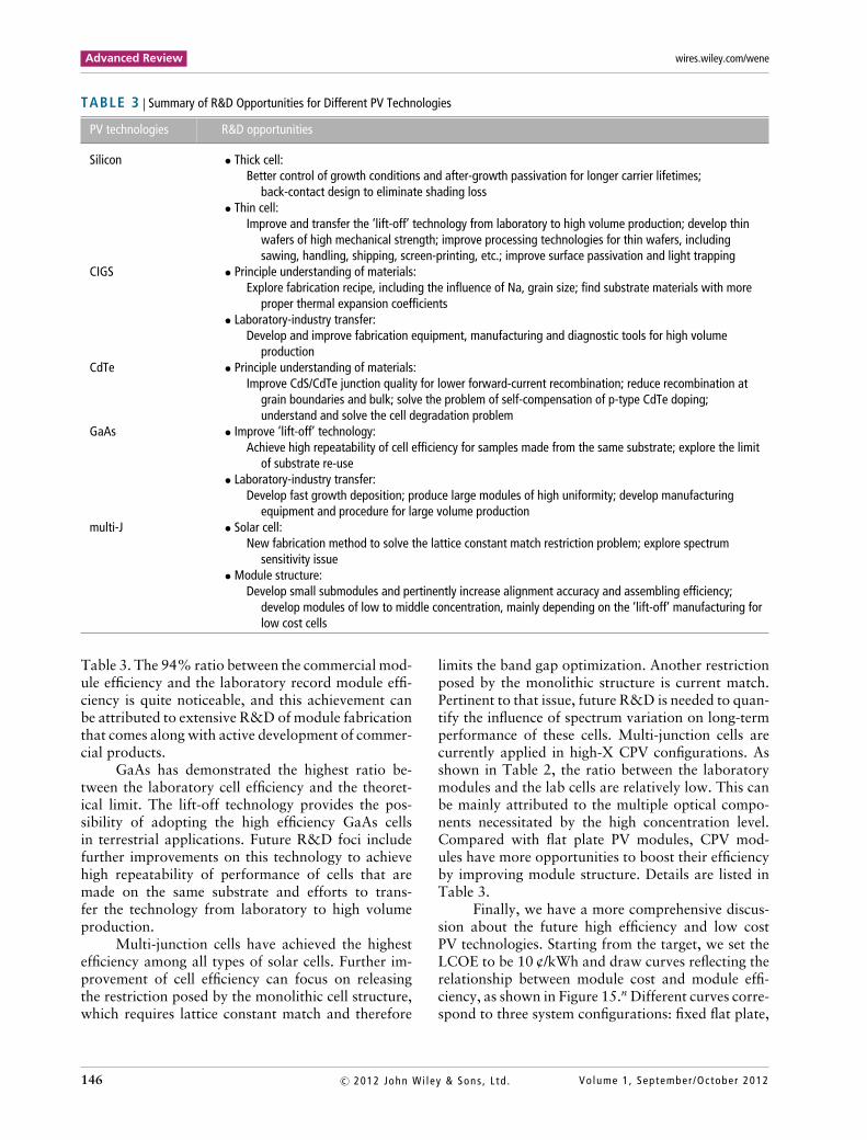
TABLE 3 Summary of R&D Opportunities for Different PV Technologies
PV technologies R&D opportunities
Silicon • Thick cell:Better control of growth conditions and after-growth passivation for longer carrier lifetimes;
back-contact design to eliminate shading loss• Thin cell:
Improve and transfer the ‘lift-off’ technology from laboratory to high volume production; develop thinwafers of high mechanical strength; improve processing technologies for thin wafers, includingsawing, handling, shipping, screen-printing, etc.; improve surface passivation and light trapping
CIGS • Principle understanding of materials:Explore fabrication recipe, including the influence of Na, grain size; find substrate materials with more
proper thermal expansion coefficients• Laboratory-industry transfer:
Develop and improve fabrication equipment, manufacturing and diagnostic tools for high volumeproduction
CdTe • Principle understanding of materials:Improve CdS/CdTe junction quality for lower forward-current recombination; reduce recombination at
grain boundaries and bulk; solve the problem of self-compensation of p-type CdTe doping;understand and solve the cell degradation problem
GaAs • Improve ‘lift-off’ technology:Achieve high repeatability of cell efficiency for samples made from the same substrate; explore the limit
of substrate re-use• Laboratory-industry transfer:
Develop fast growth deposition; produce large modules of high uniformity; develop manufacturingequipment and procedure for large volume production
multi-J • Solar cell:New fabrication method to solve the lattice constant match restriction problem; explore spectrum
sensitivity issue• Module structure:
Develop small submodules and pertinently increase alignment accuracy and assembling efficiency;develop modules of low to middle concentration, mainly depending on the ‘lift-off’ manufacturing forlow cost cells
Table 3. The 94% ratio between the commercial mod-ule efficiency and the laboratory record module effi-ciency is quite noticeable, and this achievement canbe attributed to extensive R&D of module fabricationthat comes along with active development of commer-cial products.
GaAs has demonstrated the highest ratio be-tween the laboratory cell efficiency and the theoret-ical limit. The lift-off technology provides the pos-sibility of adopting the high efficiency GaAs cellsin terrestrial applications. Future R&D foci includefurther improvements on this technology to achievehigh repeatability of performance of cells that aremade on the same substrate and efforts to trans-fer the technology from laboratory to high volumeproduction.
Multi-junction cells have achieved the highestefficiency among all types of solar cells. Further im-provement of cell efficiency can focus on releasingthe restriction posed by the monolithic cell structure,which requires lattice constant match and therefore
limits the band gap optimization. Another restrictionposed by the monolithic structure is current match.Pertinent to that issue, future R&D is needed to quan-tify the influence of spectrum variation on long-termperformance of these cells. Multi-junction cells arecurrently applied in high-X CPV configurations. Asshown in Table 2, the ratio between the laboratorymodules and the lab cells are relatively low. This canbe mainly attributed to the multiple optical compo-nents necessitated by the high concentration level.Compared with flat plate PV modules, CPV mod-ules have more opportunities to boost their efficiencyby improving module structure. Details are listed inTable 3.
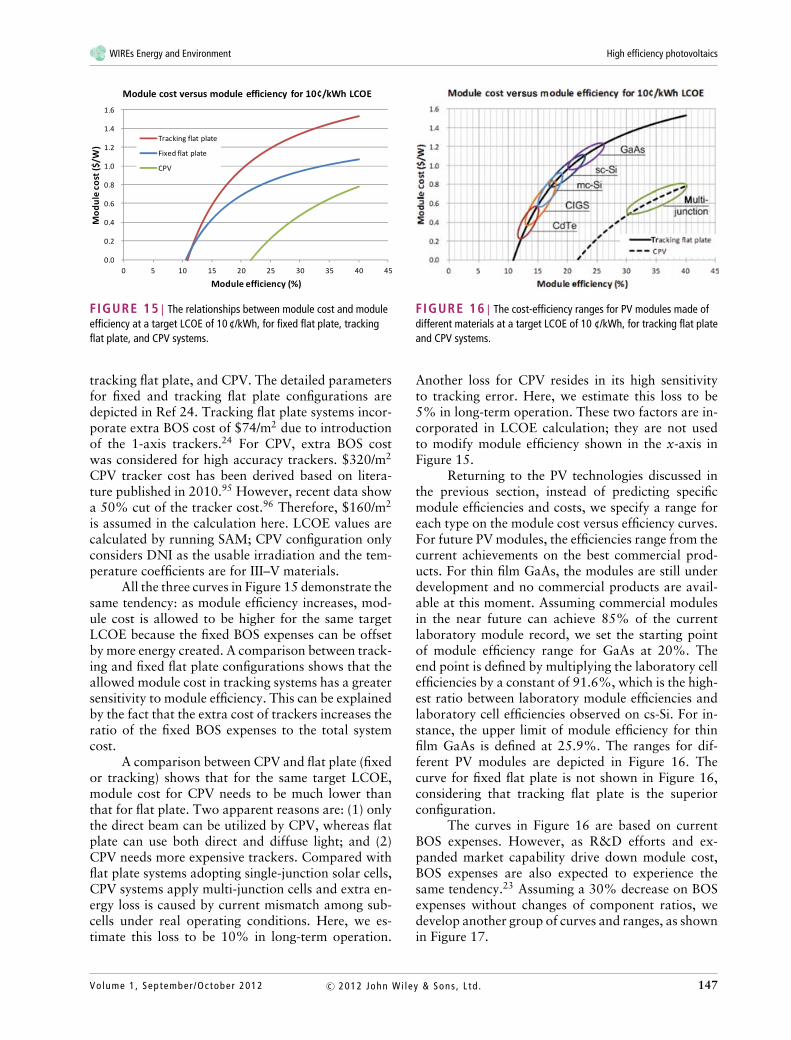
Finally, we have a more comprehensive discus-sion about the future high efficiency and low costPV technologies. Starting from the target, we set theLCOE to be 10 ¢/kWh and draw curves reflecting therelationship between module cost and module effi-ciency, as shown in Figure 15.n Different curves corre-spond to three system configurations: fixed flat plate,
146 Volume 1, September /October 2012c© 2012 John Wi ley & Sons , L td .
WIREs Energy and Environment High efficiency photovoltaics
0.0
0.2
0.4
0.6
0.8
1.0
1.2
1.4
1.6
0 5 10 15 20 25 30 35 40 45
Mod
ule
cost
($/W
)
Module efficiency (%)
Module cost versus module efficiency for 10¢/kWh LCOE
Tracking flat plate
Fixed flat plate
CPV
FIGURE 15 | The relationships between module cost and moduleefficiency at a target LCOE of 10 ¢/kWh, for fixed flat plate, trackingflat plate, and CPV systems.
tracking flat plate, and CPV. The detailed parametersfor fixed and tracking flat plate configurations aredepicted in Ref 24. Tracking flat plate systems incor-porate extra BOS cost of $74/m2 due to introductionof the 1-axis trackers.24 For CPV, extra BOS costwas considered for high accuracy trackers. $320/m2
CPV tracker cost has been derived based on litera-ture published in 2010.95 However, recent data showa 50% cut of the tracker cost.96 Therefore, $160/m2
is assumed in the calculation here. LCOE values arecalculated by running SAM; CPV configuration onlyconsiders DNI as the usable irradiation and the tem-perature coefficients are for III–V materials.
All the three curves in Figure 15 demonstrate thesame tendency: as module efficiency increases, mod-ule cost is allowed to be higher for the same targetLCOE because the fixed BOS expenses can be offsetby more energy created. A comparison between track-ing and fixed flat plate configurations shows that theallowed module cost in tracking systems has a greatersensitivity to module efficiency. This can be explainedby the fact that the extra cost of trackers increases theratio of the fixed BOS expenses to the total systemcost.
A comparison between CPV and flat plate (fixedor tracking) shows that for the same target LCOE,module cost for CPV needs to be much lower thanthat for flat plate. Two apparent reasons are: (1) onlythe direct beam can be utilized by CPV, whereas flatplate can use both direct and diffuse light; and (2)CPV needs more expensive trackers. Compared withflat plate systems adopting single-junction solar cells,CPV systems apply multi-junction cells and extra en-ergy loss is caused by current mismatch among sub-cells under real operating conditions. Here, we es-timate this loss to be 10% in long-term operation.
FIGURE 16 | The cost-efficiency ranges for PV modules made ofdifferent materials at a target LCOE of 10 ¢/kWh, for tracking flat plateand CPV systems.
Another loss for CPV resides in its high sensitivityto tracking error. Here, we estimate this loss to be5% in long-term operation. These two factors are in-corporated in LCOE calculation; they are not usedto modify module efficiency shown in the x-axis inFigure 15.
Returning to the PV technologies discussed inthe previous section, instead of predicting specificmodule efficiencies and costs, we specify a range foreach type on the module cost versus efficiency curves.For future PV modules, the efficiencies range from thecurrent achievements on the best commercial prod-ucts. For thin film GaAs, the modules are still underdevelopment and no commercial products are avail-able at this moment. Assuming commercial modulesin the near future can achieve 85% of the currentlaboratory module record, we set the starting pointof module efficiency range for GaAs at 20%. Theend point is defined by multiplying the laboratory cellefficiencies by a constant of 91.6%, which is the high-est ratio between laboratory module efficiencies andlaboratory cell efficiencies observed on cs-Si. For in-stance, the upper limit of module efficiency for thinfilm GaAs is defined at 25.9%. The ranges for dif-ferent PV modules are depicted in Figure 16. Thecurve for fixed flat plate is not shown in Figure 16,considering that tracking flat plate is the superiorconfiguration.
The curves in Figure 16 are based on currentBOS expenses. However, as R&D efforts and ex-panded market capability drive down module cost,BOS expenses are also expected to experience thesame tendency.23 Assuming a 30% decrease on BOSexpenses without changes of component ratios, wedevelop another group of curves and ranges, as shownin Figure 17.
Volume 1, September /October 2012 147c© 2012 John Wi ley & Sons , L td .
Advanced Review wires.wiley.com/wene
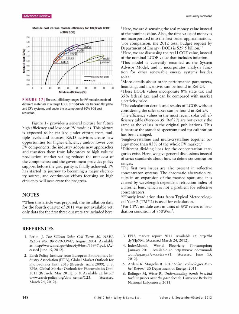
FIGURE 17 | The cost-efficiency ranges for PV modules made ofdifferent materials at a target LCOE of 10¢/kWh, for tracking flat plateand CPV systems, and under the assumption of 30% BOS costreduction.
Figure 17 provides a general picture for futurehigh efficiency and low cost PV modules. This pictureis expected to be realized under efforts from mul-tiple levels and sources: R&D activities create newopportunities for higher efficiency and/or lower costPV components; the industry adopts new approachesand transfers them from laboratory to high volumeproduction; market scaling reduces the unit cost ofthe components; and the government provides policysupport before the grid parity is finally achieved. PVhas started its journey to becoming a major electric-ity source, and continuous efforts focusing on highefficiency will accelerate the progress.
NOTESaWhen this article was prepared, the installation datafor the fourth quarter of 2011 was not available yet;only data for the first three quarters are included here.
bHere, we are discussing the real money value insteadof the nominal value. Also, the time value of money isnot incorporated into the first-order approximation.cFor comparison, the 2012 total budget request byDepartment of Energy (DOE) is $29.5 billion.18
dHere, we are discussing the real LCOE value, insteadof the nominal LCOE value that includes inflation.eThis model is currently renamed as the SystemAdvisor Model, and it incorporates analysis func-tion for other renewable energy systems besidessolar.f More details about other performance parameters,financing, and incentives can be found in Ref 24.gThese LCOE values incorporate 8% state tax and35% federal tax, and can be compared with marketelectricity price.hThe calculation details and results of LCOE withoutconsidering the sales taxes can be found in Ref 24.iThe efficiency values in the most recent solar cell ef-ficiency table (Version 39; Ref 27) are not exactly thesame as the values in the original publications. Thisis because the standard spectrum used for calibrationhas been changed.jSingle-crystalline and multi-crystalline together oc-cupy more than 85% of the whole PV market.2kDifferent dividing lines for the concentration cate-gories exist. Here, we give general discussions insteadof strict standards about how to define concentrationranges.lThe first two issues are also present in reflectiveconcentrator systems. The chromatic aberration re-sults in an expansion of the focused spot, and it iscaused by wavelength-dependent refraction index ofa Fresnel lens, which is not a problem for reflectiveconcentrators.mHourly irradiation data from Typical Meteorologi-cal Year 2 (TMY2) is used for calculation.nFor CPV, module cost in units of $/W refers to irra-diation condition of 850W/m2.
REFERENCES
1. Perlin, J. The Sillicon Solar Cell Turns 50. NRELReport No. BR-520-33947; August 2004. Availableat: http://www.nrel.gov/docs/fy04osti/33947.pdf. (Ac-cessed June 15, 2012).
2. Earth Policy Institute from European Photovoltaic In-dustry Association (EPIA), Global Market Outlook forPhotovoltaics Until 2013 (Brussels: April 2009), p. 3;EPIA, Global Market Outlook for Photovoltaics Until2015 (Brussels: May 2011), p. 8. Available at: http://www.earth-policy.org/data_center/C23. (AccessedMarch 24, 2012).
3. EPIA market report 2011. Available at: http://ht.ly/8Jp9M. (Accessed March 24, 2012).
4. IndexMundi. World Electricity Consumption;January 2011. Available at: http://www.indexmundi.com/g/g.aspx?c=xx&v=81. (Accessed June 15,2012).
5. Ardani K, Margolis R. 2010 Solar Technologies Mar-ket Report. US Department of Energy; 2011.
6. Bolinger M, Wiser R. Understanding trends in windturbine prices over the past decade. Lawrence BerkeleyNational Laboratory; 2011.
148 Volume 1, September /October 2012c© 2012 John Wi ley & Sons , L td .
WIREs Energy and Environment High efficiency photovoltaics
7. International Energy Agency. Trends in photovoltaicapplications survey report of selected IEA countriesbetween 1992 and 2010. Report IEA-PVPS T1-20;2011.
8. SEIA, GTM. US solar market insight Report, Q3 2011.Executive Summary; 2011.
9. Laherrere JH. The Hubbert Curve: Its Strengthand Weaknesses. 2000. Available at: http://dieoff.org/page191.htm. (Accessed March 24, 2012).
10. Meyer PS, Yung JW, Ausubel JH. A Primer on logisticgrowth and substitution: the mathematics of loglet labsoftware. Technology Forecasting and Social Change1999, 61:247–271.
11. Denholm P, Margolis R. Very large-scale deploymentof grid-connected solar photovoltaics in the UnitedStates: challenges and opportunities. National Renew-able Energy Laboratory; 2006.
12. Available at: http://www.eia.gov/electricity/data/state/.(Accessed March 24, 2012).
13. Available at: http://www.eia.gov/forecasts/aeo/er/index.cfm. (Accessed March 24, 2012).
14. Rogers EM. Diffusion of Innovations. Glencoe: FreePress; 1962.
15. Byrne J, Kurdgelashvili L. Chapter 2 of Handbook ofPhotovoltaic Science and Engineering. 2nd ed. Chich-ester, West Sussex, UK: John Wiley & Sons; 2011.
16. Barbose G, Darghouth N, Wiser R, Seel J. Tracking thesun IV: an historical summary of the installed cost ofphotovoltaics in the United States from 1998 to 2010.Lawrence Berkeley National Laboratory; 2011.
17. Zwaan B, Rabl A. Prospects for PV: a learning curveanalysis. Solar Energy 2003, 74:19–31.
18. Office of Chief Financial Officer. Department of En-ergy FY 2012 Congressional Budget Request. DOE/CF-0059; 2012.
19. Available at: http://www.nrel.gov/ncpv/images/efficiency_chart.jpg. (Accessed March 24, 2012).
20. Schmieder K, Haughn C, Pulwin Z, Dyer D, Bar-clay L, Doty M, Ebert C, Barnett A. Analysis of highgrowth rate MOCVD structures by solar cell devicemeasurements and time-resolved photoluminescence.37th IEEE Photovoltaic Specialists Conference; 2011.
21. Short W, Packey D, Holt T. A manual for the economicevaluation of energy efficiency and renewable energytechnologies. NREL/TP-462-5173; 1995.
22. Available at: https://sam.nrel.gov/. (Accessed March24, 2012).
23. Bony L, Doig S, Hart C, Maurer E, Newman S. Achiev-ing low-cost solar PV: industry workshop recommen-dations for near-term balance of system cost reduc-tions. 2010.
24. Wang X, Kurdgelashvili L, Byrne J, Barnett A. Thevalue of module efficiency in lowering the levelized costof energy of photovoltaic systems. Renewable and Sus-tainable Energy Reviews 2011, 15:4248–4254.
25. Zhao J, Wang A, Green MA, Ferrazza F. Novel 19.8%efficient “honeycomb” textured multicrystalline and24.4% monocrystalline silicon solar cells. Appl PhysLett 1998, 73:1991–1993.
26. Zhao J, Wang A, Yun F, Zhang G, Roche DM, Wen-ham SR, Green MA. 20,000 PERL silicon cells for the“1996 world solar challenge” solar car race. ProgrPhotovoltaics: Res Appl 1997, 5:269–276.
27. Green MA, Emery K, Hishikawa Y, Warta W, DunlopED. Solar cell efficiency tables (version 39) progress inphotovoltaics. Res Appl 2012, 20:12–20.
28. Tiedje T, Yablonovitch E, Cody GD, Brooks BG. Limit-ing efficiency of silicon solar cells. IEEE Trans ElectronDevices 1984, 31:711–716.
29. Available at: http://en.wikipedia.org/wiki/File:PV_Technology.png. (Accessed March 24, 2012).
30. Schultz O, Glunz SW, Willeke GP. Multicrystalline sil-icon solar cells exceeding 20% efficiency. Progr Pho-tovoltaics: Res Appl 2004, 12:553–558.
31. Saitoh T, Hashigami H, Rein S, Glunz S. Overview oflight degradation research on crystalline silicon solarcells. Progr Photovoltaics: Res Appl 2000, 8:535–547.
32. Tobıas I, Canizo CD, Alonso J. Chapter 7 of Hand-book of Photovoltaic Science and Engineering. 2nded. Chichester, West Sussex, UK: John Wiley & Sons;2011.
33. Sopori BL, Deng X, Benner JP, Rohatgi A, Sana P,Estreicher SK, Park YK, Roberson MA. Hydrogenin silicon: a discussion of diffusion and passivationmechanisms. Solar Energy Mater Solar Cells 1996,41/42:159–169.
34. Available at: http://global.sunpowercorp.com/products/solar-panels/. (Accessed March 24, 2012).
35. Verlinden P, Sinton RA, Wickham K, Crane RA, Swan-son RM. Backside-contact silicon solar cells with im-proved efficiency for the ‘96 world solar challenge. Pro-ceedings of the 14th EPVSC; 1997, 96–99.
36. Aberle AG. Surface passivation of crystalline silicon so-lar cells: a review. progress in photovoltaics. Res Appl2000, 8:473–487.
37. Green M. Chapter 6 of Silicon Solar Cells: AdvancedPrinciples and Practice. Centre for Photovoltaic De-vices and Systems, University of New South Wales,Sydney; 1995.
38. Henley F, Lamm A, Kang S, Liu Z, Tian L. Direct filmtransfer (DFT) technology for kerf-free silicon wafer-ing. Proceedings of the 22nd EU PVSEC; 2008, 1090–1093.
39. Hopman S, Fell A, Mayer K, Mesec M, Willeke GP,Kray D. First results of wafering with laser chemicalprocessing. Proceedings of the 22nd EU PVSEC; 2008,1131–1135.
40. Brendel R. A novel process for ultrathin monocrys-talline silicon solar cells on glass. Proceedings of 14thEU PVSEC; 1997, 1354–1357.
Volume 1, September /October 2012 149c© 2012 John Wi ley & Sons , L td .
Advanced Review wires.wiley.com/wene
41. Petermann JH, Zielke D, Schmidt J, Haase F, Rojas EG,Brendel R. 19%-efficient and 43 μm-thick crystallineSi solar cell from layer transfer using porous silicon.Progr Photovoltaics: Res Appl 2012, 20:1–5.
42. Shafarman W, Siebentritt S, Stolt L. Chapter 13 ofHandbook of Photovoltaic Science and Engineering.2nd ed. Chichester, West Sussex, UK: John Wiley &Sons; 2011.
43. Repins I, Contreras MA, Egaas B, DeHart C, ScharfJ, Perkins CL, To B, Noufi R. 19.9% EfficientZnO/CdS/CuInGaSe2 solar cell with 81.2% fill factor.Progr Photovoltaics: Res Appl 2008, 16:235–239.
44. Hedstrom J, Ohlsen H, Bodegard M, Kylner A,Stolt L, Hariskos D, Ruckh M, Schock HW.ZnO/CdS/Cu(In,Ga)Se2 thin film solar cells with im-proved performance. Proceedings of the 23rd IEEEPVSC 1993, 364–371.
45. Kronik L, Cahen D, Schock H. Effects of sodium onpolycrystalline Cu(In,Ga)Se2 and its solar cell perfor-mance. Adv Mater 1998, 10: 31–36.
46. Niles D, Al-Jassim M, Ramanathan K. Direct obser-vation of Na and O impurities at grain surfaces ofCuInSe2 thin films. J Vacuum Sci Technol A 1999,17:291–296.
47. Boyd D, Thompson D. Kirk-Othmer Encyclopaedia ofChemical Technology, 3rd ed. New York, USA: JohnWiley & Sons, Inc. 1980, 11:807–880.
48. Kessler F, Herrmann D, Powalla M. Approaches toflexible CIGS thin-film solar cells. Thin Solid Films2005, 480/481:491–498.
49. Yan Yanfa, Jiang C-S, Noufi R, Wei Su-Huai,Moutinho HR, Al-Jassim MM. Electrically benign be-havior of grain boundaries in polycrystalline CuInSe2films. Phys Rev Lett 2007, 99:235504.
50. Hetzer MJ, Strzhemechny YM, Gao M, Contreras MA,Zunger A, Brillson LJ. Direct observation of copperdepletion and potential changes at copper indium gal-lium diselenide grain boundaries. Appl Phys Lett 2005,86:162105.
51. Lei C, Li CM, Rockett A, Robertson IM. Grain bound-ary compositions in Cu(InGa)Se2. J Appl Phys 2007,101:024909.
52. Yan Y, Noufi R, Al-Jassim M. Grain-boundary physicsin polycrystalline CuInSe2 revisited: experiment andtheory. Phys Rev Lett 2006, 96:205501.
53. Seto J. The electrical properties of polycrystalline sili-con films. J Appl Phys 1975, 46:5247.
54. Siebentritt S, Schuler S. Defects and transport in thewide gap chalcopyrite CuGaSe2. J Phys Chem Solids2003, 64:1621–1626.
55. Available at: http://en.wikipedia.org/wiki/First_Solar.(Accessed March 24, 2012).
56. Available at: http://www.firstsolar.com/∼/media/WWW/Files/Downloads/PDF/Datasheet_s3_NA.ashx. (Ac-cessed March 24, 2012).
57. McCandless BE, Sites JR. Chapter 14 of Handbook ofPhotovoltaic Science and Engineering. 2nd ed. Chich-ester, West Sussex, UK: John Wiley & Sons; 2011.
58. Wei S, Zhang X. Chemical trends of defect formationand doping limit in II-VI semiconductors: the case ofCdTe. Phys Rev B 2002, 66:155211.
59. Castaldini A, Cavallini A, Fraboni B. Deep energy lev-els in CdTe and CdZnTe. J Appl Phys 1998, 83:2121–2126.
60. Stollwerck G, Sites J. Analysis of CdTe back contactbarriers. Proceedings of the 13th EU PVSEC; 1995,2020–2022.
61. Kayes BM, Nie H, Twist R, Spruytte SG, Reinhardt F,Kizilyalli IC, Higashi GS. 27.6% Conversion efficiency,a new record for single-junction solar cells under 1 sunillumination. Proceedings of 37th IEEE PVSC; 2011.
62. Available at: http://en.wikipedia.org/wiki/Concentrated_photovoltaics. (Accessed March 24, 2012).
63. Torrey E, Ruden P, Cohen P. Performance of asplit-spectrum photovoltaic device operating undertime-varying spectral conditions. J Appl Phys 2011,109:074909.
64. Geisz JF, Friedman DJ, Ward JS, Duda A, OlavarriaWJ, Moriarty TE, Kiehl JT, Romero MJ, Norman AG,Jones KM. 40.8% Efficient inverted triple-junction so-lar cell with two independently metamorphic junctions.Appl Phys Lett 2008, 93:123505.
65. Geisz JF, Kurtz S, Wanlass MW, Ward JS, Duda A,Friedman DJ, Olson JM, McMahon WE, Moriarty TE,Kiehl JT. High-efficiency GaInP/GaAs/InGaAs triplejunction solar cells grown inverted with a metamorphicbottom junction. Appl Phys Lett 2007, 91:023502.
66. Friedman DJ, Olson JM, Kurtz S. Chapter 8 of Hand-book of Photovoltaic Science and Engineering. 2nded. Chichester, West Sussex, UK: John Wiley & Sons;2011.
67. Available at: http://rredc.nrel.gov/solar/spectra/am1.5/ASTMG173/ASTMG173.html. (Accessed March 24,2012).
68. Brown A, Green M. Detailed balance limit for the seriesconstrained two terminal tandem solar cell. Physica E2002, 14:96–100.
69. Shockley W, Queisser H. Detailed Balance limit of ef-ficiency of P-N junction solar cells. J Appl Phys 1961,32:510.
70. Henry C. Limiting efficiencies of ideal single and multi-ple energy gap terrestrial solar cells. J Appl Phys 1980,51:4494.
71. Wang X, Barnett A. Value of module efficiency inreal operating conditions for low energy cost PV sys-tems. 37th IEEE Photovoltaic Specialists Conference;2011.
72. Wang X, Barnett A. The effect of spectrum variationon the energy production of triple-junction solar cells.J Photovoltaics (in review).
150 Volume 1, September /October 2012c© 2012 John Wi ley & Sons , L td .
WIREs Energy and Environment High efficiency photovoltaics
73. Muller M, Marion B, Kurtz S, Rodriguez J. An inves-tigation into spectral parameters as they impact CPVmodule performance. Proceedings of the 6th Interna-tional Conference on Concentrating Photovoltaic Sys-tems 2010, 307–311.
74. Peharz G, Siefer G, Araki K, Bett AW. Spectrometricoutdoor characterization of CPV modules using iso-type monitor cells. Proceedings of the 33rd IEEE PVSC2008, 1–5.
75. Philipps S, Peharz G, Hoheisel R, Hornung T, Al-abbadi NM, Dimroth F, Bett AW. Energy harvesting ef-ficiency of III-V triple-junction concentrator solar cellsunder realistic spectral conditions. Solar Energy Mate-rials Solar Cells 2010, 94:869–877.
76. Chan N, Young T, Brindley H, Chaudhuri B, Ekins-Daukes NJ. Variation in spectral irradiance and theconsequences for multi-junction concentrator photo-voltaic systems. Proceedings of the 35th IEEE PVSC2010, 003008–003012.
77. Kinsey G, Nayak A, Liu M, Garboushian V. Increasingpower and energy in Amonix CPV solar power plants.Journal of Photovoltaics 2011, 1:213–218.
78. Dobbin A, Georghiou G, Lumb M, Norton M, TibbitsT. Energy Harvest Predictions for a Spectrally TunedMultiple Quantum Well. 7th International CPV Con-ference; 2011.
79. Dimroth F, Baur C, Bett AW, Meusel M, Strobl G.3–6 Junction photovoltaic cells for space and terres-trial concentrator applications. Proceedings of the 31stIEEE PVSC 2005, 525–529.
80. Torrey E, Krohn J, Ruden P, Cohen P. Efficiencyof a lateral engineered architecture for photovoltaics.Proceedings of the 35th IEEE PVSC 2010, 002978–002983.
81. Vincenzi D, Busato A, Stefancich M, Martinelli G.Concentrating PV system based on spectral separa-tion of solar radiation. Physica Status Solidi (A) 2009,206:375–378.
82. Barnett A, Wang X, Waite N, Murcia P, Honsberg C,Kirkpatrick D, Laubacher D, Kiamilev F, Goossen K,Wanlass M, et al. Initial test bed for very high efficiencysolar cells. Proceedings of the 33rd IEEE PVSC 2008,1–7.
83. Wang X, , Waite N, Murcia P, Emery K, Steiner M,Kiamilev F, Goossen K, Honsberg C, Barnett A. Lateralspectrum splitting concentrator photovoltaics: directmeasurement of component and submodule efficiency.Progr Photovoltaics: Res Appl 2012, 20:149–165.
84. McCambridge J, Steiner M, Unger B, Emery K, Chris-tensen E, Wanlass M, Gray A, Takacs L, Buelow R,McCollumT, et al. Compact spectrum splitting pho-tovoltaic module with high efficiency. Progr Photo-voltaics: Res Appl 2011, 19:352–360.
85. Lucovsky G. Photoeffects in nonuniformly irradiatedP-N junctions. J Appl Phys 1960, 31:1088.
86. Kurtz S. Estimating and controlling chromatic aberra-tion losses for two-junction, two-terminal devices in re-fractive concentrator systems. Proceedings of the 25thIEEE PVSC 1996, 361–364.
87. Ota Y, Nishioka K. Three-dimensional simulationof concentrator photovoltaic modules using raytraceand equivalent circuit simulators. Solar Energy 2012,86:476–481.
88. Sala G, Anton I. Chapter 10 of Handbook of Photo-voltaic Science and Engineering. 2nd ed. Chichester,West Sussex, UK: John Wiley & Sons; 2011.
89. Available at: http://www.lapptannehill.com/suppliers/literature/3m/Factors.pdf. (Accessed March 24, 2012).
90. Available at: http://www.semprius.com/news_pr.php.(Accessed March 24, 2012).
91. Bower CA, Menard E, Garrou PE. Transfer printing: anapproach for massively parallel assembly of microscaledevices. Proceedings of the 58th ECTC 2008, 1105–1109.
92. Burroughs S, Conner R, Furman B, Menard E, Gray A,Meitl M, Bonafede S, Kneeburg D, Ghosal K, BukovnikR, Wagner W, Seel S. A new approach for a low costCPV module design utilizing micro-transfer printingtechnology. Proceedings of the 6th International Con-ference on Concentrating Photovoltaic Systems 2010,163–166.
93. Ebert C, Parekh A, Pulwin Z, Zhang W, Lee D, ByrnesD. Fast growth rate GaAs and InGaP for MOCVDgrown triple junction solar cells. Proceedings of the35th IEEE PVSC 2010, 002007–002011.
94. Furman B, Menard E, Gray A, Meitl M, BonafedeS, Kneeburg D, Ghosal K, Bukovnik R, Wagner W,Gabriel J, et al. A high concentration photovoltaicmodule utilizing micro-transfer printing and surfacemount technology. Proceedings of the 35th IEEEPVSC 2010, 000475–000480.
95. Seshan C. CPV: not just for hot deserts. Proceedings ofthe 35th IEEE PVSC 2010, 003075–003080.
96. Available at: http://www.alibaba.com/product-gs/450240568/CPV_sun_tracker_solar_system.html. (Acce-ssed March 24, 2012).
Volume 1, September /October 2012 151c© 2012 John Wi ley & Sons , L td .