high-performance current-controlled quadrature oscillator ... papers/midem_46(2016)2p91.pdf ·...
TRANSCRIPT
91
Original scientific paper
MIDEM Society
High-performance Current-Controlled Quadrature Oscillator Using an optimized CCIISamir Ben Salem1,4, Achwek Ben Saied3,4 and Dorra Sellami Masmoudi2,4
1Development Group in Electronics and Communications (EleCom) Laboratory of Electronics and Information Technology (LETI), Sfax, Tunisia 2Computor Imaging and Electronic Systems Group (CIEL), Research Unit on Intelligent Design and Control of complex Systems (ICOS), Sfax, Tunisia 3Research Center for Computer Science & Multimedia of Sfax (CETIC), Sfax, Tunisia4University of Sfax, National Engineering School of Sfax (ENIS), Sfax, Tunisia
Abstract: This paper proposes two structures of current-controlled quadrature Sinusoidal oscillator in CMOS technology (Voltage mode “VM” and Voltage/Current mode “VCM”). Thanks to its high degree of controllability, the translinear second-generation current conveyor is used as a basic block for our oscillator. The proposed circuit employs three optimized translinear second-generation current conveyors (CCII). The oscillation condition and the oscillation frequency are independently controllable by bias current. The proposed Quadrature Oscillator frequency can be tuned in the range of [285 MHz – 844 MHz] by a simple variation of a DC bias current. ADS (Advanced Design System) simulation results are performed using CMOS 0.18 μm process of TSMC.
Keywords: Voltage Mode Current-controlled Oscillators; Standard CMOS current conveyor; Voltage/Current Mode Current Controlled Oscillators; CMOS 0.18 μm process of TSMC; optimized CCII.
Visoko učinkovit tokovno krmiljen kvadrantni oscilator z optimiziranim CCIIIzvleček: Članek predlaga dve strukturi tokovno krmiljenega kvadrantnega sinusnega oscilatorja v CMOS tehnologiji (napetostni – VM in napetostno tokovni – VCM). Zaradi velike zmožnosti nadzorovanja je za osnovni blok oscilatorja uporabljen translinearen tokovni krmilnik druge generacije (CCII). Frekvenca oscilacije je neodvisno določljiva z enosmerno komponento toka v območju od 285 – 844 MHz. Simulacijski rezultati so narejeni v CMOS 0.18 μm tehnologiji TSMC
Ključne besede: napetostni tokovno krmiljen oscilator; standardni CMOS tokovni krmilnik; napetostno tokovni oscilator; CMOS; CCII.
* Corresponding Author’s e-mail: [email protected]
Journal of Microelectronics, Electronic Components and MaterialsVol. 46, No. 2(2016), 91 – 99
1 Introduction
Variable-frequency quadrature Oscillators are basic sig-nal-generating blocks frequently needed in communi-cation systems. The LC or RC quadrature oscillator pres-ents many problems in the literature such as problems of integration, limitations of Surface Acoustic Wave, impedance matching, tuning, linearity, phase noise, … etc. For this reason, the voltage and current-controlled resistors (VCR and ICR) are widely used to replace float-ing or grounding resistors. The literature abounds with approaches implementing VCR and ICR [2-3]. Some structures use the OTA (Operational Transconductance Amplifier) [1], circuit-based on MOS transistors operat-
ing in saturation region [4]. Nevertheless, these circuits suffer from their dependence to absolute temperature and their small input voltage range and complexity of control. Second-generation current-conveyor (CCII) based resistor blocs provide a working solution to solve these problems [5-6].
In order to enhance the performance, minimize the noise effect provoked by the floating and grounding resistor, get controllable characteristics for the pro-posed Quadrature oscillator, translinear second-gen-eration, current-controlled conveyor based structures seem to be the most efficient [7-8]. These structures
92
present a higher degree of CCII characteristics control [9-10]. This family of CCII is first proposed in bipolar technology [9-11]. Recently, the translinear CCII family was extended to MOS submicron technologies going towards VLSI design. Reaching submicron technolo-gies, the MOS transistor becomes able to achieve high transit frequencies [12-15]. These CCII’s structures are used in different radio frequency (RF) controllable ap-plications such as oscillators, quadrature oscillators and filters [10-15].
This paper is organized as follows: In section II, we pres-ent the characteristics of optimized translinear Second Generation Current Conveyors. Simulation results of an optimized translinear second generation current conveyor are highlighted in section III (implemented in 0.18μm CMOS technology). In section IV, we pres-ent the CCII based quadrature oscillator architecture. We introduce the proposed Controlled Quadrature Oscillator in section V. Finally, the proposed structure is designed and simulated using ADS (Advanced Design System) software.
2 The optimized transinear loop-based ccii configurations
Figure1: General representation of a current conveyor
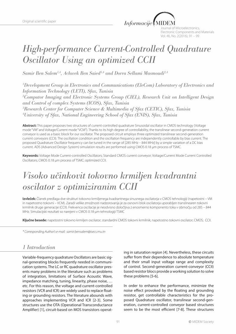
The CCII is a three-terminal active block. Its general rep-resentation is shown in Figure 1. The CCII ensures two functionalities between its terminals:A Current follower between terminals X and Z.A Voltage follower between terminals X and Y.
In order to get ideal transfers, a CCII should be charac-terized by low impedance on terminal X and high im-pedance on terminals Y and Z.
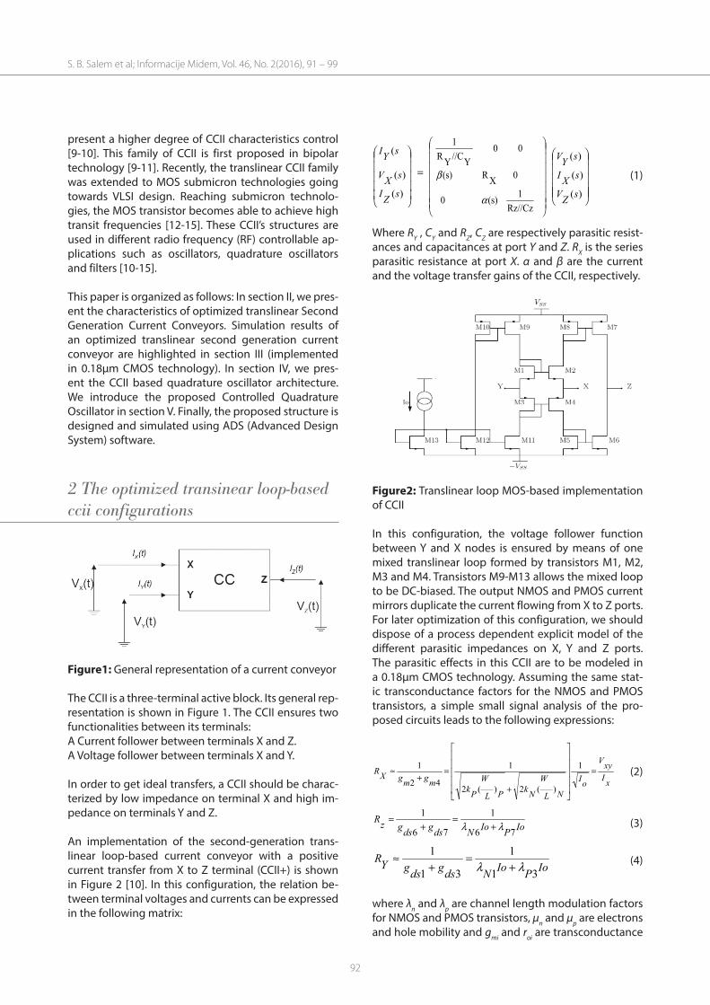
An implementation of the second-generation trans-linear loop-based current conveyor with a positive current transfer from X to Z terminal (CCII+) is shown in Figure 2 [10]. In this configuration, the relation be-tween terminal voltages and currents can be expressed in the following matrix:
)(
)(
(
sZI
sXV
sYI
Rz//Cz
1 (s) 0
0 XR (s)
0 0 Y//CYR
1
α
β
)(
)(
)(
sZV
sXI
sYV= (1)
Where RY , CY and RZ, CZ are respectively parasitic resist-ances and capacitances at port Y and Z. RX is the series parasitic resistance at port X. α and β are the current and the voltage transfer gains of the CCII, respectively.
Figure2: Translinear loop MOS-based implementation of CCII
In this configuration, the voltage follower function between Y and X nodes is ensured by means of one mixed translinear loop formed by transistors M1, M2, M3 and M4. Transistors M9-M13 allows the mixed loop to be DC-biased. The output NMOS and PMOS current mirrors duplicate the current flowing from X to Z ports. For later optimization of this configuration, we should dispose of a process dependent explicit model of the different parasitic impedances on X, Y and Z ports. The parasitic effects in this CCII are to be modeled in a 0.18µm CMOS technology. Assuming the same stat-ic transconductance factors for the NMOS and PMOS transistors, a simple small signal analysis of the pro-posed circuits leads to the following expressions:
xIxyV
oI
NL
W
NkPL
W
Pkmgmg
XR =
+
=+
≈ 1
)(2)(2
1
42
1 (2)
IoPIoNdsgdsg
zR76
1
76
1λλ +
=+
= (3)
IoPIoNdsgdsg
YR31
1
31
1λλ +
=+
≈ (4)
where λn and λp are channel length modulation factors for NMOS and PMOS transistors, µn and µp are electrons and hole mobility and gmi and roi are transconductance
S. B. Salem et al; Informacije Midem, Vol. 46, No. 2(2016), 91 – 99
93
and output resistance of Mi transistor, respectively, with:
oIiL
W
NorPkoIDSViiL
W
NorPkmig )(2)1()(2 ≈+= λ (5)
oIi
DSVi
oIidsig
oirλ
λ
λ≈
+==
)1(1 (6)
We can see from the above equations that entire trans-linear loop-based CCII parasitic impedances can be con-trolled by means of Io. Moreover, parasitic resistance on the X (RX) port was used in many high-frequency tuning applications. Getting lower values of this resistance can lead to higher frequency operations. In this light, we try below to ameliorate the performance of the CCII by op-timization approach. This strategy consists in minimiz-ing the X port input resistance value, maximizing the resistance values of Y and Z ports, maximizing high cut-off current (Fci) and voltage (Fcv) frequencies, minimiz-
ing noise effect (2
,outTi ) and silicon area (S), minimizing the deviation between Fci and Fcv and minimizing the deviation between α (current static gain) and β (volt-age static gain). To obtain good performance we will maximize the objective function. The objective func-tion can be expressed as follows:
βα −+
−+++++++= 8765)(*42
,
3*2*1a
ciFcvF
a
S
a
Rx
aRzRya
outTi
acvFaciFaoF (7)
Where α1,...,α8 are positive coefficients used for normali-zation.
The static current and voltage gains are given by the following equations:
EF
E
YVXV
+==β (8)
KG
XIZI ==α (9)
Where:
)54(28)42(58 dsgdsgmgmgmgmgmgmgE +++=
)42(58 dsgdsgmgmgF +≈
)425252(7)288(64 dsgmgmgdsgmgmgmgdsgdsgmgmgmgG +++++=
852548)5245
425252(8)288(54
dsgmgmgdsgmgmgdsgmgdsgmgdsgmgmgdsgmgmgmgdsgdsgmgmgmgK
++++
+++++=
The current bandwidth is given by:
DsCs*BAsiH 2 ++
==*
)( (10)
Where:
06)/r06.rm6g)(104.rm4g-(1A ++=
)gs5Cgs6Cgd4(C04.rgs4CB ++=
m5gm5.g04.rm4gD +=
)C gs6C gs5C gs4
C gd4r04).gm5.C gs4gm4
).C gs5C gs6C gd4(((C
+++
++++= +
and
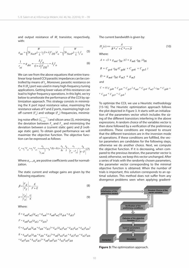
To optimize the CCII, we use a Heuristic methodology [15-16]. The Heuristic optimization approach follows the plot depicted in Figure 3. It starts with an initializa-tion of the parameters vector which includes the siz-ing of the different transistors interfering in the above expressions. A random choice of the variables vector is then done followed by a verification of the preliminary conditions. These conditions are imposed to ensure that the different transistors are in the inversion mode of operations. If these conditions are fulfilled, the vec-tor parameters are candidates for the following steps, otherwise we do another choice. Next, we compute the objective function. If it is decreasing, when com-pared to the previous iteration, the parameter vector is saved; otherwise, we keep this vector unchanged. After a series of trials with the randomly chosen parameters, the parameter vector corresponding to the minimal objective function is obtained. When the number of trials is important, this solution corresponds to an op-timal solution. This method does not suffer from any divergence problems seen when applying gradient-
Figure 3: The optimization approach.
S. B. Salem et al; Informacije Midem, Vol. 46, No. 2(2016), 91 – 99

94
based methods, but its efficiency is closely related to the number of iterations. Indeed, with a high number of trials, we manage to explore in a simple random way all the proposed tuning range of the different param-eters and good performances are ensured. Finally, we simulate the performances of the optimized CCII. If it is correct we take the optimal parameters else we go to the correction phase.
We notice that the optimization process can be done with a ±1.5V supply voltage and 100µA bias current (table 1). The obtained optimal transistor sizes are re-ported in table 2.
Table 1: Simulation conditions
Technology 0.18 μm CMOS TSMCSupply voltage 1.5 VBias current 100 μA
TabIe 2: Optimal device sizing
Device Name Aspect ratio W/L (µm)
M1, M2 6.1/0.18M3, M4 27.45/0.18Mxx (in PMOS current mirrors) 13.725/0.18Mxx (in NMOS current mirrors) 3.05/0.18
3 Simulation results
The optimized current conveyor was simulated with ADS software. The main results obtained are represent-ed in Figure 4
A. Parasitic resistance at x terminal (Rx(Ω)) relative to Io(A)
B. Parasitic resistance at Y and Z terminals (Ry(Ω) and Rz(Ω)) relative to Io (A)
C. Voltage DC transfer characteristic of the CCII
D. Frequency response of the voltage follower Vx/Vy
E. Current DC transfer characteristic of the CCII
S. B. Salem et al; Informacije Midem, Vol. 46, No. 2(2016), 91 – 99
95
G. current and voltage gains versus Io (Bi and Bv pre-sent respectively αand β)
Figure 4: Performance of the optimized CCII
ADS software simulations of the translinear loop based CCII in Figure 2 were conducted under the optimal parameters. The parasitic resistance at port X is repre-sented in Figure 4.A versus Io. It is obvious that RX can be controlled in the range [200Ω, 1.6kΩ] by varying Io in the range [1µA, 400µA]. The fact that should be under-scored is that, even though this structure has a lower RX when compared to the value given in [11, 15]. Fig-ure 4.A depicts results obtained from both simulations (RX) and MAPLE theoretical calculus of (RXthe). We notice a good agreement between both characteristics. Fig-ure 4.B depicts the parasitic resistance values RZ and RY versus the bias current Io. Accordingly, tunable charac-teristics can be obtained while higher values of these parasitic resistances are preserved.
Figure 4.C and Figure 4.E display the DC transfer char-acteristics of the optimized CCII. The voltage transfer can be linear between -0.7V and 0.7V. Moreover, the bandwidths of output terminals are shown in Figure 4.D and Figure 4.F. The −3dB bandwidths of Iz/Ix and Vx /Vy are located at 4.33GHz and 2.77GHz, respectively. Figure 4.G indicates that α and β (current and voltage gains) are close to unity. The remaining other static and
dynamic characteristics of the optimized translinear configuration are summarized in table 3.
Table 3: Performance characteristics of the optimized CCII with Io = 100µA and 1.5 supply voltage
Voltage gain β 0.943Current gain α 1.1
Fci 2.7GHzFcv 4.33GHz
Relative current Error 0.15%Relative Voltage Error 0.093%
Input Impedance(RY//CY ) 18KΩ//87fFInput Impedance(Rz // Cz ) 24KΩ//25fF
Input Resistance Rx 380ΩThe offset current -2.2µAThe offset voltage 13mV
It is noticeable that the optimized configuration yields a high current and voltage cut-off frequencies. This structure is a promising building block for the design of RF blocs such as the controlled quadrature oscillator.
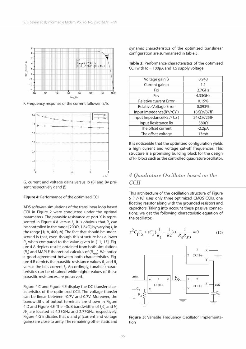
4 Quadrature Oscillator based on the CCII
This architecture of the oscillation structure of Figure 5 [17-18] uses only three optimized CMOS CCIIs, one floating resistor along with the grounded resistors and capacitors. Taking into account these passive connec-tions, we get the following characteristic equation of the oscillator:
034
1)2
1
4
1(5512 =+−+
XRRRRsCCCs (12)
Figure 5: Variable Frequency Oscillator Implementa-tion
F. Frequency response of the current follower Iz/Ix
S. B. Salem et al; Informacije Midem, Vol. 46, No. 2(2016), 91 – 99
96
This leads to the following oscillation condition and os-cillation frequency, respectively:
24 RR ≥ (13)
43512
10
RXRCCf
π= (14)
In the reality R2 and R4 are respectively given by these relations: (R2+ Rx1) and (R4 + Rx2). If one of the values var-ies after implementation, we can recover the correct value by Io1 or Io2.
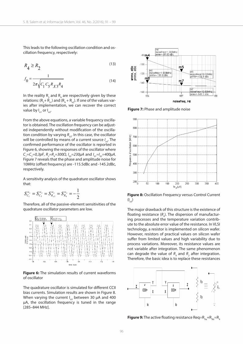
From the above equations, a variable frequency oscilla-tor is obtained. The oscillation frequency can be adjust-ed independently without modification of the oscilla-tion condition by varying RX3. In this case, the oscillator will be controlled by means of a current source Io3. The confirmed performance of the oscillator is reported in Figure 6, showing the responses of the oscillator where C1=C5=0,3pF, R2=R4=300Ω, I03=230µA and I01=I02=400µA. Figure 7 reveals that the phase and amplitude noise for 10MHz (offset frequency) are -115.5dBc and -145.2dBc, respectively.
A sensitivity analysis of the quadrature oscillator shows that:
21
4351−==== oo
x
oo wR
wR
wC
wC SSSS
Therefore, all of the passive-element sensitivities of the quadrature oscillator parameters are low.
Figure 6: The simulation results of current waveforms of oscillator
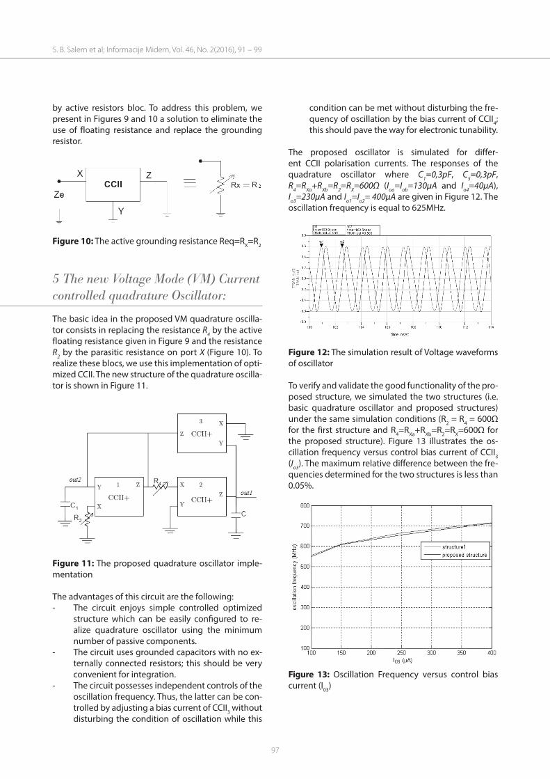
The quadrature oscillator is simulated for different CCII bias currents. Simulation results are shown in Figure 8. When varying the current Io3 between 30 μA and 400 μA, the oscillation frequency is tuned in the range [285–844 MHz].
Figure 8: Oscillation Frequency versus Control Current (Io3)
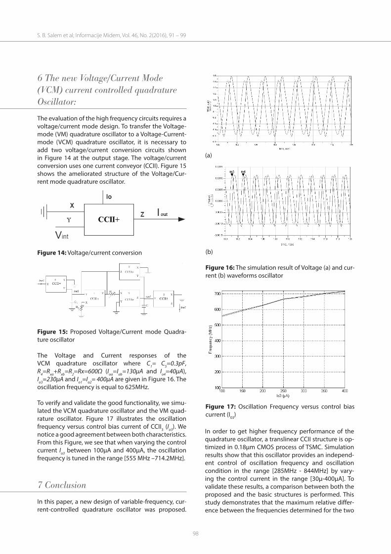
The major drawback of this structure is the existence of floating resistance (R4). The dispersion of manufactur-ing processes and the temperature variation contrib-ute to the absolute error value of the resistance. In VLSI technology, a resistor is implemented on silicon wafer. However, resistors of practical values on silicon wafer suffer from limited values and high variability due to process variations. Moreover, its resistance values are not variable after integration. The same phenomenon can degrade the value of R4 and R2 after integration. Therefore, the basic idea is to replace these resistances
Figure 7: Phase and amplitude noise
Figure 9: The active floating resistance Req=RXa+RXb=R4
S. B. Salem et al; Informacije Midem, Vol. 46, No. 2(2016), 91 – 99
97
by active resistors bloc. To address this problem, we present in Figures 9 and 10 a solution to eliminate the use of floating resistance and replace the grounding resistor.
Figure 10: The active grounding resistance Req=RX=R2
5 The new Voltage Mode (VM) Current controlled quadrature Oscillator:
The basic idea in the proposed VM quadrature oscilla-tor consists in replacing the resistance R4 by the active floating resistance given in Figure 9 and the resistance R2 by the parasitic resistance on port X (Figure 10). To realize these blocs, we use this implementation of opti-mized CCII. The new structure of the quadrature oscilla-tor is shown in Figure 11.
Figure 11: The proposed quadrature oscillator imple-mentation
The advantages of this circuit are the following:- The circuit enjoys simple controlled optimized
structure which can be easily configured to re-alize quadrature oscillator using the minimum number of passive components.
- The circuit uses grounded capacitors with no ex-ternally connected resistors; this should be very convenient for integration.
- The circuit possesses independent controls of the oscillation frequency. Thus, the latter can be con-trolled by adjusting a bias current of CCII3 without disturbing the condition of oscillation while this
condition can be met without disturbing the fre-quency of oscillation by the bias current of CCII4; this should pave the way for electronic tunability.
The proposed oscillator is simulated for differ-ent CCII polarisation currents. The responses of the quadrature oscillator where C1=0,3pF, C5=0,3pF, R4=RXa+RXb=R2=RX=600Ω (Ioa=Iob=130µA and Io4=40µA), Io3=230µA and Io1=Io2= 400µA are given in Figure 12. The oscillation frequency is equal to 625MHz.
Figure 12: The simulation result of Voltage waveforms of oscillator
To verify and validate the good functionality of the pro-posed structure, we simulated the two structures (i.e. basic quadrature oscillator and proposed structures) under the same simulation conditions (R2 = R4 = 600Ω for the first structure and R4=RXa+RXb=R2=RX=600Ω for the proposed structure). Figure 13 illustrates the os-cillation frequency versus control bias current of CCII3 (Io3). The maximum relative difference between the fre-quencies determined for the two structures is less than 0.05%.
Figure 13: Oscillation Frequency versus control bias current (I03)
S. B. Salem et al; Informacije Midem, Vol. 46, No. 2(2016), 91 – 99
98
6 The new Voltage/Current Mode (VCM) current controlled quadrature Oscillator:
The evaluation of the high frequency circuits requires a voltage/current mode design. To transfer the Voltage-mode (VM) quadrature oscillator to a Voltage-Current-mode (VCM) quadrature oscillator, it is necessary to add two voltage/current conversion circuits shown in Figure 14 at the output stage. The voltage/current conversion uses one current conveyor (CCII). Figure 15 shows the ameliorated structure of the Voltage/Cur-rent mode quadrature oscillator.
Figure 14: Voltage/current conversion
Figure 15: Proposed Voltage/Current mode Quadra-ture oscillator
The Voltage and Current responses of the VCM quadrature oscillator where C1= C5=0.3pF, R4=Rxa+Rxb=R2=Rx=600Ω (Ioa=Iob=130µA and Io4=40µA), Io3=230µA and Io1=Io2= 400µA are given in Figure 16. The oscillation frequency is equal to 625MHz.
To verify and validate the good functionality, we simu-lated the VCM quadrature oscillator and the VM quad-rature oscillator. Figure 17 illustrates the oscillation frequency versus control bias current of CCII3 (Io3). We notice a good agreement between both characteristics. From this Figure, we see that when varying the control current Io3 between 100μA and 400μA, the oscillation frequency is tuned in the range [555 MHz –714.2MHz].
7 Conclusion
In this paper, a new design of variable-frequency, cur-rent-controlled quadrature oscillator was proposed.
In order to get higher frequency performance of the quadrature oscillator, a translinear CCII structure is op-timized in 0.18µm CMOS process of TSMC. Simulation results show that this oscillator provides an independ-ent control of oscillation frequency and oscillation condition in the range [285MHz - 844MHz] by vary-ing the control current in the range [30µ-400µA]. To validate these results, a comparison between both the proposed and the basic structures is performed. This study demonstrates that the maximum relative differ-ence between the frequencies determined for the two
(a)
(b)
Figure 16: The simulation result of Voltage (a) and cur-rent (b) waveforms oscillator
Figure 17: Oscillation Frequency versus control bias current (I03)
S. B. Salem et al; Informacije Midem, Vol. 46, No. 2(2016), 91 – 99

99
structures is less than 0.05%. Finally we have proposed a Voltage-Current mode quadrature oscillator. Simu-lation results show that the proposed VCM oscillator presents a control oscillation frequency between [555 MHz –714.2MHz] by varying the control current in the range of [100µ-400µA]
8 References
1. KHAN, A., AHMED, A. M. T. Realization of tunable floating resistors. Electronics Letters, 1986, vol. 22, p. 799–800.
2. SAAID, O., FABRE, A. Class AB current-controlled resistor for high performance current-mode ap-plications. Electronics Letters, 1996, vol. 32, p. 4–5.
3. SENANI, R., SINGH, A. K., SINGH, V. K. A new float-ing current-controlled positive resistance using mixed translinear cells. IEEE Transactions on Cir-cuits and Systems-II, 2004, vol. 51, p.374–377.
4. G. Wilson, P. Chan, Floating CMOS resistor, IEE Electronics Letters 28 (1993) 306–307.
5. RIEWRUJA, V., PETCHMANEELUMKA, W. Floating currentcontrolled resistance converters using OTAs. International Journal of Electronics and Com-munications, 2008, vol. 62, p. 725–731.
6. M. KUMNGERN, U. TORTEANCHAI, K. DE-JHAN” Voltage-Controlled Floating Resistor Using DDCC “ Radioengineering, vol. 20, no. 1, april 2011
7. P. Beg, I. A. Khan and M. T. Ahmed, “Tunable Four Phase Voltage Mode Quadrature Oscillator using Two CMOS MOCCIIs,” Multimedia, Signal Process-ing and Communication Technologies, Aligarh, 14-16 March 2009, pp. 155-157. doi:10.1109/MSPCT.2009.5164198
8. S. Maheshwari, “Analogue Signal Processing Applica-tions Using a New Circuit Topology,” IET Circuits, De-vices & Systems, Vol. 3, No. 3, 2008, pp. 106-115.
9. A. Fabre, F. Seguin. “New second generation cur-rent conveyor with reduced parasitic resistance and Band pass filter application” IEEE transaction on circuits and systems1: fundamental theory and applications, VOL.48, NO.6, June 2001.
10. S. B. Salem, D. S. Masmoudi and M. Loulou “A Novel CCII-Based Tunable Inductance and High Frequency Current Mode Band Pass Filter Appli-cation,” Journal of Circuits, Systems, and Computers (JCSC), Vol. 15, No. 6, 2006, pp. 849-860.
11. Hassan O.Elwan and A. M. Soliman, “Low-Voltage Low-Power CMOS Current Conveyors” IEEE trans-action on circuits and systems1: fundamental theory and applications, VOL.44, NO.9, SEPTEM-BER 1997.
12. C. Thoumazou, F. J. Lidgey and D. Haigh, “Integrat-ed Circuits: The Current Mode Approach,” IEEE Cir-cuit and Systems Series 2, Peter Ltd., London, 1993.
13. P. Beg, I. A. Khan and M. T. Ahmed, “Tunable Four Phase Voltage Mode Quadrature Oscillator using Two CMOS MOCCIIs,” Multimedia, Signal Process-ing and Communication Technologies, Aligarh, 14-16 March 2009, pp. 155-157.
14. Achwek BENSAIED, Samir BEN SALEM and Dorra SELLAMI MASMOUDI “A new CMOS Current Con-trolled Quadrature Oscillator Based on a MCCII” in the Journal: Circuits and Systems ISSN2153-1285 Volume: 02; Issue: 04; Start page: 269; Date: 2011
15. S. B. Salem, M. Fakhfakh, D. S. Masmoudi, M. Lou-lou, P. Loumeau and N. Masmoudi, “A High Perfor-mances CMOS CCII and High Frequency Applica-tions,” Journal of Analog Integrated Circuits and Signal Processing, Vol. 49, No.1, 2006, pp. 71-78.
16. M. Fakhfakh, M. Loulou and N. Masmoudi, “ An Improved Algorithm-Driven Methodology To Op-timize Switched Current Memory Cells By Tran-sistor Sizing “ The IEEE Inter. Conf. on Electrical, Electronic and Computer Engineering (ICEEC’04). September, 2004. Cairo, Egypt.
17. D. Sellami Masmoudi, S. Ben Salem, M. Loulou and L. Kamoun “ A Radio Frequency CMOS Cur-rent Controlled Oscillator Based on a New Low Parasitic Resistance CCII”2004 International Con-ference on Electrical, Electronic and Computer Engineering ICCEC’04 (0-7803-8575-6/04/$20.00 ©2004 IEEE)
[18 Ben Salem, S.; Sellami Masmoudi, D.; Fakhfakh, M.; Loulou, M.; Masmoudi, N “ High frequency CCII based oscillators and multifunction filters” Design and Test of Integrated Systems in Nanoscale Tech-nology, 2006. DTIS 2006. International Confer-ence
19,. U. Torteanchai and M. Kumngern “Current-Tuna-ble Current-Mode All-pass Section Using DDCC” International Conference on Electronic Devices, Systems and Applications (ICEDSA) 2011
Arrived: 12. 07. 2015Accepted: 13. 03. 2016
S. B. Salem et al; Informacije Midem, Vol. 46, No. 2(2016), 91 – 99