high spatial resolution energy dispersive x-ray ... · dispersive x-ray spectrometry in the sem and...
TRANSCRIPT

high-resolution eds in sem
S8 Compositional Analysis Supplement May 2013 | MicroscopyandAnalysis
High spatial resolution energy dispersive X-ray spectrometry in the SEM and the detection of light elements including lithiumSimon Burgess, Xiaobing Li, and James HollandOxford Instruments NanoAnalysis, High Wycombe, UK
IntroductionEnergy-dispersive spectrometry (EDS) is the established technique for the determination of constituent elements and elemental composition on the microscale in the scanning electron microscope (SEM). The past 20 years has seen significant advances in detector technology which has improved the capability for the detection of low-energy X-rays. This has opened up new applications in the analysis of nanomaterials, and also materials containing the light elements from boron to fluorine.
Here we consider how progress in three areas, low-energy resolution, sensor size and X-ray detection efficiency, are together producing leaps forward in the sensitivity of EDS detectors to low-energy X-rays, and what current developments may offer in terms of nano- and light element analysis.
Energy ResolutionDetection of light elements by EDS became common in the 1990s with the introduction of vacuum-tight polymer windows. These were robust to normal SEM operation, but also relatively transparent to low-energy X-rays, and they extended the elemental range of EDS to include the elements boron, carbon, oxygen, nitrogen and fluorine. In combination with field-emission SEM, light-element detectors also promised analysis of smaller structures through the use of lower accelerating voltages which reduce the volume of X-ray generation within the sample [1] (Figure 1).
Resolution of EDS detectors has been improving since their commercialization in the 1970s. Resolution is measured using a radioactive 55Fe source, or Mn metal in a SEM, to produce a MnKa peak whose resolution is determined as the full width at half the height (FWHM). Detector resolution is of vital importance for low-energy analysis as spacing of the X-ray lines decreases with decreasing energy. Mn resolution was found to be a poor indicator of resolution performance at low energy due to its insensitivity to detector noise and incomplete charge collection. In 2002 a new ISO specification 15632:2002 [2] was published, stressing the need to measure EDS resolution in the SEM using carbon X-rays to guarantee low-energy performance. This requirement for low-energy X-ray performance measures encouraged the development of detectors with excellent low-energy resolution
that could easily separate common low-energy lines such as BKa and CKa.
Improved resolution was promised with the sub-130 eV headline Mn resolution promised by the new technology of silicon drift detectors (SDD) in the mid-2000s. However, early SDD technology suffered from incomplete charge collection, and was incompatible with low-energy analysis. The charge collection properties of SDD sensors have improved to match their excellent low noise to provide the promised improvements in low-energy resolution in the best sensors.
One way to test low-energy resolution is to look
at the separation of Til lines around 0.4 keV [3]. To separate these lines requires both excellent noise and charge collection for silicon-based sensors. The improvement in performance can be seen in Figure 2. The best Si(Li) detectors with Mn resolution around 125 eV could almost begin to separate these lines (green) but not if they showed any incomplete charge collection (yellow). The best SDD sensors with excellent charge collection show significant separation of these lines (red). This can aid identification of the very closely spaced lines typical of low energies.
The lightest element detectable with
Figure 1 X-ray generation volumes calculated using Monte Carlo simulation for pure iron at different accelerating voltages [1]. By reducing kV the area analysed is reduced and the spatial resolution of analysis increased.
Figure 2 Spectra collected from Ti metal at 5 kV using a 10 mm2 Si(Li) detector which shows incomplete charge collection (yellow), a 30 mm2 Si(Li) detector with excellent charge collection and the latest 50 mm2 silicon drift detector (SDD). Note the carbon peak from the 10 mm2 Si(Li) detector is shifted to lower energy due to the incomplete charge collection, and this loss of resolution means no separation of TiLn/TiLa is possible. The 30 mm2 has the same noise and Mn resolution but with much better charge collection shows better carbon peak resolution and position and separates OKa from TiLa better, the TiLn/TiLa shape is beginning to be visible. The 50 mm2 SDD, has excellent noise and charge collection. Although it is only about 3 eV better at MnKa, its resolution at CKa is over 10 eV better, and the TiLn/TiLa separation is now clear.

high-resolution eds in sem
S9MicroscopyandAnalysis | May 2013 Compositional Analysis Supplement
commercial EDS is beryllium which was first separated from detector noise in the 1980s [4]. When first reported the resolution of the BeKa peak was over 100 eV [4, 5]. However, in the time it has taken to improve Mn resolution by less than 15 eV, the resolution of the BeKa has improved by over 65 eV, with the best SDD detectors now showing peaks with resolutions around 35 eV (Figure 3).
Sensor SizeLight element containing samples are often highly beam sensitive, limiting the beam current that can be used. Reducing the accelerating voltage for improved spatial resolution means lower X-ray yields even assuming beam current can be maintained (Figure 4). For practical analysis of low-energy lines therefore traditional 10mm2 Si(Li) detectors were too small. Making larger sensors was possible, but only at the cost of resolution performance, the largest Si(Li) detectors made for low-energy analysis in SEM being 30 mm2 [6].
Developments in silicon drift sensors (SDD), have changed this in the past 5 years. Early SDD detectors were small, with very poor low-energy resolution. However, they have the capability of resolution performance which is independent of size, using designs with fixed anode dimensions where capacitance is fixed. This performance is now being realized with the release of large area SDD detectors. Currently sensors up to 150 mm2 in size are now available with low-energy resolution similar or even better than that produced by Si(Li). In combination with parallel improvements in FEG-SEM performance, this has revolutionized nanoanalysis, making X-ray mapping at 3 kV on structures less than 50 nm in size now practical (Figure 5). The gap between SEM and TEM for chemical analysis is closing.
X-ray detection efficiencyImproving sensitivity for low-energy X-rays by increasing sensor size while maintaining or even improving peak resolution, has revolutionised EDS creating a true nanoanalysis capability, however, it is unlikely to be the route for future progress. There are two barriers to progress in this
Figure 3 (left) Spectrum collected from Be metal at 5 kV using a X-MaxN 50 mm2 SDD detector. The BeKa peak is completely separated from the noise and has a FWHM of 35 eV.
Figure 4 (right)EDS spectrum simulations from pure iron at different accelerating voltages but using the same beam current and acquisition time. Reducing accelerating voltage reduces line choice for analysis to the low energy L line series and also causes a dramatic reduction in the X-ray counts emitted by the sample.
Figure 5 X-ray maps for FeLa (A), NiLa (B) and CuLa (C) collected at 3 kV from a memory alloy using a X-MaxN 150 mm2 SDD detector. (D) is a zoomed-in image where the three maps have been overlaid on the secondary electron image, showing structures as small as 21 nm are clearly distinguished.
Table 1 Improvements in detector efficiency for a windowless configuration compared to a polymer vacuum window (Moxtek AP3.3).
A B
C D
SiLl BeKa NKa OKa SiKa MnKa
Improvement x8 x3.3 x2.8 x2.1 x1.5 x1.4
high-resolution eds in sem
S10 Compositional Analysis Supplement May 2013 | MicroscopyandAnalysis
area: firstly, ballistic deficit caused by the distance charge carriers travel within the sensor, starts to reduce resolution performance at high count rate as sensor size increases [7]. Secondly, and more importantly, count rate is not only proportional to area; it is also inversely proportional to the square of the distance between sample and sensor. Enlarging sensor size is only useful for large area sensors while the tube of the detector can be made small enough to be positioned close the sample. Lens geometry and tube diameter therefore limit maximum sensor size.
Another area to improve sensitivity is to look again at the polymer thin window. Removing the window reduces X-ray attenuation, increasing intensity for low-energy X-rays, with increasing gains at very low energy (Table 1). Windowless detectors are gaining acceptance on the TEM where vacuum environments are tightly controlled. These gains have caused investigations of potential benefits for SEM also.
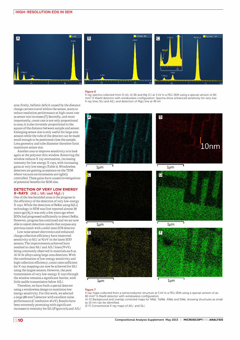
Detection of Very Low Energy X-rays (SiLl, AlLl and MgLl )One of the less heralded areas is the progress in the efficiency of the detection of very low-energy X-rays. While the detection of BeKa using Si(Li) technology in SEM was first reported almost 30 years ago [4], it was only a few years ago when SDDs had progressed sufficiently to detect BeKa. However, progress has continued and we are now able to report detection results that surpass any previous result with a solid-state EDS detector.
Low noise sensor electronics and enhanced charge collection efficiency have improved sensitivity to SiLl at 92 eV in the latest SDD sensors. The improvements achieved have resulted in clear SiLl and AlLl lines (79 eV) being commonly observed in materials such as Al-Si-Sr alloys using large-area detectors. With the combination of low-energy sensitivity and high collection efficiency, count rates sufficient for X-ray mapping can now be achieved for SiLl using the largest sensors. However, the poor transmission of very low-energy X-rays through the window remains a significant barrier, with little usable transmission below AlLl .
Therefore, we have built a special detector using a windowless design to maximize low-energy sensitivity. For this work, we selected a large (80 mm2) detector with excellent noise performance (C resolution 45 eV). Results have been extremely promising with significant increases in intensity for SiLl (Figure 6A) and AlLl
Figure 6 X-ray spectra collected from Si (A), Al (B) and Mg (C) at 5 kV in a FEG-SEM using a special version of 80 mm2 X-MaxN detector with windowless configuration. Spectra show enhanced sensitivity for very low X-ray lines SiLl and AlLl, and detection of MgLl line at 49 eV.
Figure 7 X-ray maps collected from a semiconductor structure at 3 kV in a FEG-SEM using a special version of an 80 mm2 X-MaxN detector with windowless configuration. (A-D) Background and overlap corrected maps for NKa, TaMa, AlKa and SiKa, showing structures as small as 10 nm can be identified. (E-F) Conventional X-ray maps of AlLl and SiLl .
A B
C D
E F
A B C
high-resolution eds in sem
S11MicroscopyandAnalysis | May 2013 Compositional Analysis Supplement
lines (Figure 6B), compared to detectors fitted with polymer windows.
The excellent low-energy sensitivity suggested this configuration had the potential to detect and measure even lower energy X-ray lines. In a further series of tests we have seen clear evidence of this potential. The lowest energy X-ray that has been detected with this set-up is MgLl at 49 eV. The peak is separated from noise sufficiently for element identification (Figure 6C).
X-ray Mapping of very low energy X-ray linesDetection of these very low-energy X-ray lines offers the potential to use lower accelerating voltage, further improving spatial resolution of analysis. In applications where Si and Al are important constituents, accelerating voltage can be reduced below the 3 kV needed to excite the K lines of these elements.
Figure 7 shows an example of the X-ray mapping of structures in a semiconductor with widths 10-200 nm. 10-20 nm structures containing nitrogen (silicon and titanium nitride -A) and tantalum (B) are clearly visible, with excellent NKa intensity shown (Table 1). Data collection at 3 kV allows the comparison of Ka and Ll lines for Al and Si to be made (C-F).
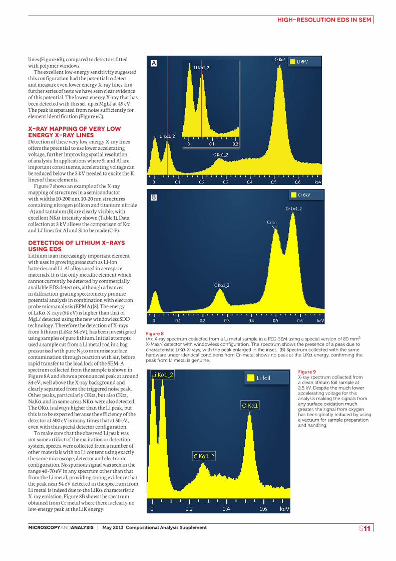
Detection of Lithium X-rays using EDS Lithium is an increasingly important element with uses in growing areas such as Li-ion batteries and Li-Al alloys used in aerospace materials. It is the only metallic element which cannot currently be detected by commercially available EDS detectors, although advances in diffraction-grating spectrometry promise potential analysis in combination with electron probe microanalysis (EPMA) [8]. The energy of LiKa X-rays (54 eV) is higher than that of MgLl detected using the new windowless SDD technology. Therefore the detection of X-rays from lithium (LiKa 54 eV), has been investigated using samples of pure lithium. Initial attempts used a sample cut from a Li metal rod in a bag pressurised with pure N2 to minimise surface contamination through reaction with air, before rapid transfer to the load lock of the SEM. A spectrum collected from the sample is shown in Figure 8A and shows a pronounced peak at around 54 eV, well above the X-ray background and clearly separated from the triggered noise peak. Other peaks, particularly OKa, but also CKa, NaKa and in some areas NKa were also detected. The OKa is always higher than the Li peak, but this is to be expected because the efficiency of the detector at 500 eV is many times that at 50 eV, even with this special detector configuration.
To make sure that the observed Li peak was not some artifact of the excitation or detection system, spectra were collected from a number of other materials with no Li content using exactly the same microscope, detector and electronic configuration. No spurious signal was seen in the range 40–70 eV in any spectrum other than that from the Li metal, providing strong evidence that the peak near 54 eV detected in the spectrum from Li metal is indeed due to the LiKa characteristic X-ray emission. Figure 8B shows the spectrum obtained from Cr metal where there is clearly no low-energy peak at the LiK energy.
Figure 9X-ray spectrum collected from a clean lithium foil sample at 2.5 kV. Despite the much lower accelerating voltage for this analysis making the signals from any surface oxidation much greater, the signal from oxygen has been greatly reduced by using a vacuum for sample preparation and handling.
Figure 8 (A): X-ray spectrum collected from a Li metal sample in a FEG-SEM using a special version of 80 mm2 X-MaxN detector with windowless configuration. The spectrum shows the presence of a peak due to characteristic LiKa X-rays, with the peak enlarged in the inset. (B) Spectrum collected with the same hardware under identical conditions from Cr-metal shows no peak at the LiKa energy, confirming the peak from Li metal is genuine.
A
B

high-resolution eds in sem
S13MicroscopyandAnalysis | May 2013 Compositional Analysis Supplement
biography Simon Burgess obtained his BSc in geochemisty from the University of St. Andrews and his PhD in geology from the University of Edinburgh. Simon worked in the EPMA unit at the University of Edinburgh before moving to Oxford Instruments as an expert in WDS. For the past 15 years Simon has worked on the development of EDS and WDS hardware, software and applications.
abstractCurrent technology for energy-dispersive X-ray spectrometry using silicon-drift detectors in combination with the latest field-emission scanning electron microscopes delivers routine nanoscale characterisation of structures as small as 50 nm. This performance relies on a combination of high spectral resolution and large sensor area. Results from the latest developments in low-noise electronics and windowless detectors show the possibility of analysing structures down to 10 nm and the sensitive detection of light elements, including, for the first time, lithium.
acknowledgementsThe authors would like to thank Fibics Inc for supplying the semiconductor device, Hitachi High Technology Corp. for the use of their vacuum sample preparation and SEM loading facility, and Peter Statham of Oxford Instruments NanoAnalysis for help and advice preparing this paper.
Corresponding author details Dr Simon Burgess,Oxford Instruments NanoAnalysis,Halifax Road,High Wycombe, Bucks, HP12 3SE, UKTel: +44 (0) 1494 442255Email: [email protected]
Microscopy and Analysis 27(4):S8-S13 (EU), 2013
©2013 John Wiley & Sons, Ltd
study has shown that by combining large sensor area, low noise electronics, and windowless SDD technology, detection and X-ray mapping of very low-energy X-rays is feasible. In addition X-rays from lithium have been detected and analysed by EDS in SEM for first time.
Clearly, further work is required to determine the applicability of this new technology to real application problems, particularly in the case of lithium. More information is also required to understand the design requirements necessary for successful commercialization of this technology.
References1. Barkshire, I. et al. High-spatial-resolution low-energy electron beam X-ray microanalysis. Mikrochim. Acta 132:113-128, 2000.2. ISO15632:2002, ISO, Switzerland, 2002.3. Statham, P. Measuring Performance of Energy-Dispersive X-ray Systems. Microsc. Microanal. 4:605-615, 1999.4. Statham, P. Accuracy, reproducibility and scope for X-ray microanalysis with Si(Li) detectors. Journal de Physique 45:C2-175 - C2-180, 1984.5. Statham, P. Instrumental considerations for EDX Microanalysis at Intermediate Voltages. In: Intermediate voltage electron microscopy and its application to materials science, Ed: K Rajan, Philips Electronic Instruments Inc, New Jersey, pp 3-10, 1987.6. Burgess, S. et al. X-ray Analysis of Nano-structures Using the INCAPentaFET-x3 Si(Li) detector. Microsc. Microanal. 13(S02):1438-1439, 2007.7. Bell, D. et al. Low Voltage Electron Microscopy,
lithium compounds formed on lithium metal Li metal is reactive to a number of gases that the sample was exposed to during preparation including N2 to form Li3N and atmospheric water vapour to form LiOH [9]. Therefore further tests have been conducted on a Li-foil sample that was prepared and loaded through a special microscope loading process under vacuum and argon. Spectra collected from this sample (Figure 9 at 2.5 kV) show significantly lower levels of OKa, allowing lower kV to be used. The benefit of this method was shown by exposing this sample to air for 10 minutes. This exposure results in a rapid alteration to oxygen and carbon containing species, forming characteristic hexagonal structures (Figure 10A). X-ray maps collected for LiKa, CKaand OKa after exposure (Figure 10 B-D), show the formation of lithium carbonates and oxides/hydroxides in these regions during exposure to air.
ConclusionsBy combining large sensor size and excellent low-energy resolution, modern silicon drift detector-based energy-dispersive X-ray spectrometry systems in combination with the latest field-emission scanning electron microscopes provide ever more detailed views of nanoscale structures. With current technologies structures in the range less than 50 nm can be investigated at 3 kV.
To achieve even greater detector sensitivity in the future, to further improve spatial resolution, may require the use of windowless detectors to reduce the loss of X-rays due to attenuation. This
Figure 10(A) Secondary electron image collected on a lithium foil sample after deliberate exposure to air for 10 minutes showing characteristic hexagonal areas of reaction. Area of X-ray map collection is shown by the red box. The X-ray maps were collected at 2.5 kV and are shown for LiKa (B), CKa (C) and OKa (D). The X-ray maps show in the areas of reaction the formation of Li carbonates and oxides/hydroxides.
Principles and Applications, Wiley, pp 185-200, 20138. Terauchi, M. et al. Ultrasoft-X-ray emission spectroscopy using a newly designed wavelength-dispersive spectrometer attached to a transmission electron microscope. Journal of Electron Microscopy 61(1):1-8, 2012.9. Wietelmann, U., Bauer, R. J. Lithium and Lithium Compounds. Ullmann’s Encyclopedia of Industrial Chemistry, Wiley, 2000.
A B
C D