high speed and energy efficient hardware architectures for lte
TRANSCRIPT

High speed and energy efficient
hardware architectures for LTE-advanced
systems
by
Chinmaya Mahapatra
A THESIS SUBMITTED IN PARTIAL FULFILLMENT OF
THE REQUIREMENTS FOR THE DEGREE OF
MASTER OF APPLIED SCIENCE
in
The Faculty of Graduate and Postdoctoral Studies (Electrical & Computer Engineering)
THE UNIVERSITY OF BRITISH COLUMBIA
(Vancouver)
October 2013
© Chinmaya Mahapatra, 2013
ii
Abstract
The explosive growth of internet traffic, fueled by an ever increasing availability of
mobile wireless devices and demands of end users to be always connected, provides a
challenge for cellular and broadband wireless access technologies. In this thesis, we present
novel approaches of physical layer architectures Orthogonal Wavelet Division Multiple
Access (OWDMA) & Fast Inverse Square Root based Matrix Inverse (FISRMI) that is
shown to substantially improve bit error rate (BER), increase data rate, accommodating more
number of users, low power consumption and cover dead zones effectively. The work
presented in this thesis consists of basically two parts which provides solutions to different
problems in the Long Term Evolution (LTE) networks.
In LTE-Advanced (LTE-A), heterogeneous networks (HetNet) concept using
centralized coordinated multipoint (CoMP) transmitting Radio resources over optical fibers
LTE-A Radio-Over-Fiber (ROF) has provided a feasible way of satisfying user demands. A
OWDMA processor architecture is proposed and evaluated. To validate the architecture,
circuit is designed and synthesized on a Xilinx vertex-6 Field Programmable Gate Array
(FPGA). We compare our architecture with similar available architectures for resource
utilization & timing and provide performance comparison with OFDMA for different quality
metrics of communication systems. The OWDMA architecture is found to perform better
than OFDMA for BER performance versus signal to noise ratio (SNR) in ROF media. It also

iii
gives higher throughput and mitigates the bad effect of Peak to Average Power ratio (PAPR)
and Inter carrier interference (ICI).
Secondly, a low complexity and high speed matrix inversion algorithm FISRMI using
fast inverse square root based on QR-decomposition and systolic array was designed. Matrix
operations are costliest computational module within multiple input multiple output
(MIMO)-LTE receivers. The capital expenditure (CAPEX) is reduced by implementing a
4x4 matrix inverse in Xilinx Virtex-6 FPGA by optimizing the module for speed and power
by pipelining. The results are compared with state of art techniques of Coordinate Rotation
Digital Computer (CORDIC) based algorithms and the various Minimum Mean Squared
Error channel matrices of size 4x4 and 8x8 are inverted at different bit precision on a BER
plot.

iv
Preface
Co-authorship statement
I hereby declare that I am the main contributor and first author of this manuscript, as
well as the related papers published [1, 2] written in collaboration with Dr. Thanos Stouraitis,
Prof. Victor C.M. Leung, Ashwin Ramakrisnan and Saad Mehboob at the University of
British Columbia. These papers stemmed from portions of and findings in parts of Chapters 1
– 4 of this thesis. I also contributed as second author in [3] with Saad Mahboob where i
helped in formulating the capacity equation for Massively Distributed Antenna Systems.
I also led the efforts in producing a journal manuscript from the research
contributions documented in Chapters 3, co-authored with Dr. Thanos Stouraitis and Prof.
Victor C.M. Leung, entitled, „„An Orthogonal Wavelet Division Multiple Access Processor
Architecture for LTE-Advanced Radio-over-Fiber Systems over Heterogeneous Networks”.
My primary responsibilities in our collaboration included identifying and formulating
the research questions and proposed schemes, performing literature reviews to map out
previous works, designing the test bed to support our research, preparing and submitting
conference papers and journal manuscripts to peer-review our findings and results, and
preparing this thesis manuscript. The contributions of Dr. Thanos Stouraitis and Prof. Victor
C.M. Leung included refining the research problem formulation, assisting with resolving
technicalities of the algorithms published in conferences and submitted to Journal and
providing invaluable paper and manuscript edits, revisions and suggestions.
v
Table Of Contents
Abstract .......................................................................................................................... ii
Preface ........................................................................................................................... iv
Table Of Contents ......................................................................................................... v
List Of Tables................................................................................................................ ix
List Of Figures ............................................................................................................... x
List Of Abbreviations ................................................................................................ xiii
Acknowledgements ................................................................................................. xviii
Dedication ................................................................................................................... xix
1. Introduction ........................................................................................................ 1
1.1 Objectives & Motivations .......................................................................... 1
1.2 Technical Issues ....................................................................................... 2
1.3 Research Contributions ............................................................................ 4
1.4 Outline Of The Thesis .............................................................................. 6
2. Background ........................................................................................................ 7
2.1 Evolution Of Wireless Standard ............................................................... 7
2.2 Long Term Evolution ................................................................................ 9
2.3 Protocol Architecture .............................................................................. 10
2.3.1 SAE Technology.......................................................................... 11
2.3.2 E-UTRAN Architecture ................................................................ 12
2.4 LTE PHY Layer ....................................................................................... 13
2.4.1 Channel Coding........................................................................... 14
2.4.2 Physical Channel (PDSCH) Processing .................................... 16
2.4.3 Scrambling ................................................................................... 16

vi
2.4.4 Modulation ................................................................................... 16
2.4.5 Codebook Precoding................................................................... 16
2.4.6 LTE Frame Structure................................................................... 17
2.4.7 Resource Element Mapping ....................................................... 17
2.4.8 Cell-Specific Reference Signals ................................................. 19
2.4.9 OFDMA ........................................................................................ 19
2.4.10 SC-FDMA..................................................................................... 20
2.4.11 Downlink Physical Layer Procedures ......................................... 21
2.4.12 Uplink Physical Layer Procedures.............................................. 21
2.4.13 Receiver UE Processing ............................................................. 22
2.5 LTE Advanced: Proposed Key Areas For Improvement ...................... 23
2.6 LTE Advance Techniques ...................................................................... 24
2.6.1 Heterogeneous Networks ........................................................... 24
2.6.2 Carrier Aggregation (CA) ............................................................ 25
2.6.3 Coordinated Multipoint (CoMP) .................................................. 27
2.6.4 Enhanced MIMO ......................................................................... 28
2.7 Cellular Architectures ............................................................................. 29
2.7.1 Micro Base Station Architecture ................................................. 29
2.7.2 Femtocell Architecture ................................................................ 31
2.7.3 Broadband Radio Over Fiber Distributed Antenna System
Architecture.................................................................................. 33
2.8 Wavelets in Wireless Communications ................................................. 36
2.8.1 Flexibility Of Orthogonal Wavelet System ................................. 37
2.8.2 Wavelet Based Downlink Scheduling In LTE Systems ............. 38
2.8.3 Wavelet Based PAPR Reduction In OFDMA Systems ............. 38
2.8.4 Low Complexity In Wavelet Based System As Compared To
OFDMA ........................................................................................ 39
2.8.5 Wavelet Based Multi Carrier Multiple Access Scheme For
Cognitive Radio ........................................................................... 39
2.9 Literature Review Of MIMO-LTE Matrix Inversion Algorithms ............. 40
2.10 Summary ................................................................................................. 41

vii
3. A Orthogonal Wavelet Division Multiple Access Processor
Architecture For LTE-A Radio-Over-Fiber HetNet Systems...................... 43
3.1 Overview Of OWDMA ............................................................................ 43
3.2 Orthogonal Wavelet Division Multiplexing............................................. 44
3.2.1 Formulation Of OWDM From The 9/7- Filter Using Lifting........ 45
3.2.2 Sequential Output-Based Parallel Processing Architecture
For OWDM................................................................................... 47
3.3 Proposed OWDMA Processor Architecture For LTE A-ROF Layer
1 ............................................................................................................... 49
3.3.1 Scheduler..................................................................................... 54
3.3.2 Core Unit ...................................................................................... 54
3.3.3 Control Unit .................................................................................. 56
3.3.4 Coefficient Generator Unit .......................................................... 57
3.4 Pipelining The Parallel Architecture For Low Power ............................ 59
3.5 Performance Results And Comparisons ............................................... 62
3.5.1 Synthesis Of Proposed Architecture & Resource Utilization .... 62
3.5.2 Comparison With Various Architectures .................................... 63
3.6 Quality Metric Comparison In 4G LTE-Radio-Over-Fiber System ....... 67
3.6.1 Bit-Error-Rate Comparison ......................................................... 71
3.6.2 Throughput Of OWDMA System ................................................ 76
3.6.3 Peak Average To Power Ratio ................................................... 79
3.6.4 Inter Carrier Interference............................................................. 80
3.7 Summary ................................................................................................. 82
4. Fast Inverse Square Root Based Matrix Inverse For MIMO-LTE
Systems............................................................................................................. 84
4.1 Matrix Inversion Using QR Decomposition And Systolic Array........... 85
4.1.1 QR Decomposition Using Givens Rotation ................................ 85
4.1.2 Fast Inverse Square Root ........................................................... 87
4.1.3 Systolic Architecture.................................................................... 89
4.2 FPGA Implementation And Analysis ..................................................... 92
4.3 LTE MIMO MMSE Matrix Inversion BER .............................................. 96

viii
4.4 Summary ................................................................................................. 98
5. Conclusion........................................................................................................ 99
5.1 Summary Of Contributions..................................................................... 99
5.2 Future Directions .................................................................................. 100
5.3 Final Remarks....................................................................................... 101
Bibliography .............................................................................................................. 102
Appendix A................................................................................................................. 108
Appendix B................................................................................................................. 112

ix
List Of Tables
Table 2.1: LTE specifications (© 2008 3GPP) ............................................................ 10
Table 3.1: Forward odd coefficients ............................................................................. 58
Table 3.2: Forward even coefficients ........................................................................... 59
Table 3.3: FPGA resource consumption summary for OWDMA ................................ 63
Table 3.4: Comparison between various 1-D architectures ....................................... 65
Table 3.5: Resource utilization for OFDMA & OWDMA processors .......................... 66
Table 3.6: Simulation parameters ................................................................................ 71
Table 3.7: Fiber parameters in optical link................................................................... 76
Table 4.1: Comparisons of computational operations ................................................ 94
Table 4.2: Resource estimation of 4x4 matrix inversion core..................................... 95
Table A.1: Test hardware requirements .................................................................... 110
Table A.2: Lab test equipment ................................................................................... 110
Table A.3: Software tools ........................................................................................... 111

x
List Of Figures
Figure 2.1: Overview of present and future wireless communication systems
[9], [10], [11] .............................................................................................. 8
Figure 2.2: SAE (system architecture evolution) and LTE network, from
http://www.artizanetworks.com/lte_tut_sae_tec.html (© 2012Artiza
Networks, Inc.) ........................................................................................ 12
Figure 2.3: Radio interface protocol architecture around the physical layer [13]
(© 2008 3GPP). ...................................................................................... 13
Figure 2.4: Overview of uplink physical channel processing [14] (©2008 3GPP)
................................................................................................................. 15
Figure 2.5: Overview of downlink physical channel processing [14] (©2008
3GPP)...................................................................................................... 15
Figure 2.6: Radio frame structure for LTE [14] (©2008 3GPP) .............................. 17
Figure 2.7: Channel bandwidth parameter of LTE................................................... 17
Figure 2.8: Resource allocated per user in time and frequency [14] (©2008
3GPP)...................................................................................................... 18
Figure 2.9: OFDMA vs SC-FDMA [14] (©2008 3GPP). .......................................... 20
Figure 2.10: Carrier aggregation [16] (©2011 3GPP)................................................ 26
Figure 2.11: Base station cooperation: intersite and intrasite CoMP. [17] (©2011
IEEE) ...................................................................................................... 27
Figure 2.12: Femto cell architecture [5] (©2011 IEEE).............................................. 32
Figure 2.13: Broadband radio over fiber distributed antenna system architecture
[5] (©2011 IEEE) .................................................................................... 34

xi
Figure 3.1: Signal to noise ratio versus bit error rate comparison for various
orthogonal wavelet families. [51] (©2008 IEEE) ................................... 46
Figure 3.2: The core filter unit showing 9-tap and 7-tap FIR filter structure with
input X[N]. ............................................................................................... 51
Figure 3.3: The top level Generic OWDMA processor implementation block
diagram. .................................................................................................. 53
Figure 3.4: Timing diagram showing logical signals with clock............................... 55
Figure 3.5: Symmetric boundary extension of input data........................................ 56
Figure 3.6: Control logic finite state machine implementation ................................ 57
Figure 3.7: Deployment diagram of 4G LTE-A ROF systems having
centralized architecture. (a) Overview of centralized eNB
architechture . (b) Transmitter unit. (c) Receiver unit. .......................... 69
Figure 3.8: Signal to noise ratio versus bit error rate comparison for OWDMA
and OFDMA architectures in LTE A ROF systems. (a) Signal to
noise ratio versus bit error rate comparison for rate-1/2 turbo-
coded & uncoded QPSK-OWDMA and QPSK-OFDMA. (b) Signal
to noise ratio versus bit error rate comparison for rate-1/2 turbo-
coded & uncoded 16QAM-OWDMA and 16QAM-OFDMA. (c)
Signal to noise ratio versus bit error rate comparison for rate-1/2
turbo-coded & uncoded 64QAM-OWDMA and 64QAM-OFDMA. (d)
Signal to noise ratio (radio-over-fiber) versus bit error rate
comparison for QPSK-OWDMA and QPSK-OFDMA at different
fiber lengths. ........................................................................................... 75
Figure 3.9: Signal to noise ratio versus throughput (spectral efficiency) for
OWDMA and OFDMA systems at different values of M ...................... 78
Figure 3.10: CCDF plot of PAPR in dB ...................................................................... 80
Figure 3.11: Frequency offset model.......................................................................... 80
Figure 3.12: ICI power of OWDM & OFDM systems ................................................. 82

xii
Figure 4.1: 2’s Complement signed form of floating point numbers with
exponent and mantissa .......................................................................... 87
Figure 4.2: Block diagram of hardware model ......................................................... 91
Figure 4.3: Systolic array architecture...................................................................... 92
Figure 4.4: (a) 16-QAM MMSE decoder using CORDIC 16 & 20-bit and
floating point based FISRMI algorithm. (b) 64-QAM MMSE decoder
using CORDIC 16 & 20-bit and floating point based FISRMI
algorithm. ................................................................................................ 97
Figure A.1: Test bed experimental setup................................................................ 109

xiii
List Of Abbreviations
3GPP 3rd Generation Partnership Project
ACK/NACK Acknowledge/Not Acknowledge
ADC Analog to Digital Converter
AMC Advanced Mezzanine Card
AMPS Advanced Mobile Phone System
ARQ Automatic Repeat request
AWGN Additive White Gaussian Noise
BER Bit Error Rate
BRAM Block Random Access Memory
CA Carrier Aggregation
CAPEX Capital Expenditure
CCDF Complementary Cumulative Distribution
CDMA Code Division Multiple Access
CLB Configuration Logic Block
CMOS Complementary Metal Oxide Semiconductor
CoMP Coordinated Multipoint
CORDIC Coordinate Rotation Digital Computer
CP Cyclic Prefix
CPRI Common Public Radio Interface
CPU Central Processing Unit

xiv
CQI Channel Quality Indications
CRC Cyclic redundancy Check
CWT Continuous Wavelet Transform
DAC Digital to Analog Converter
DAS Distributed Antenna Systems
DFT Discrete Fourier Transform
DLSCH Downlink Shared Channel
DSP Digital Signal Processing
DWT Discrete Wavelet Transform
E-UTRAN Evolved Universal Terrestrial Radio Access
eICIC Enhanced Inter Cell Interference Coordination
eNB evolved Node Base Station
EPA Extended Pedestrian A Model
ETACS European Total Access Communication
FDD Frequency Division Duplex
FFT Fast Fourier Transform
FISRMI Fast Inverse Square Root based Matrix Inverse
FM Frequency modulation
FPGA Field Programmable Gate Array
GPRS General Packet Radio Service
GSM Global System for Mobile Communications
HARQ Hybrid Automatic Repeat request
HeNB Heterogeneous Node Base station
HetNet Heterogeneous Networks

xv
HSDPA High-speed Downlink Packet Access
HSPA High-speed Packet Access
HSUPA High-speed Uplink Packet Access
ICI Inter Carrier Interference
IEEE Institute of Electrical and Electronics Engineers
IFFT Inverse Fast Fourier Transform
IOB Input/Output Block
IP Internet Protocol
ISI Inter Symbol Interference
ISM Industrial, Scientific and Medical
ITU International Telecommunication Union
LTE Long Term Evolution
LTE-A Long Term Evolution- Advanced
MAC Medium Access Control
MAN Metro Area Networks
MIMO Multiple Input and Multiple Output
MMSE Minimum Mean Squared Error
NZDSF Non-Zero Dispersion Shifted Fiber
OBSAI Open Base Station Architecture Initiative
OFDMA Orthogonal Frequency Division Multiple Access
OPEX Operational Expenditure
OWDMA Orthogonal Wavelet Division Multiple Access
PAPR Peak to Average Power ratio
PCI Pre-coding Control Information

xvi
PDCCH Physical Downlink Control Channel
PHICH Physical Hybrid ARQ Indicator Channel
PHY Physical
PMI Pre-coding Matrix Indicator
PON Passive Optical Network
PRB Physical Resource Block
PUCCH Physical Uplink Control Channel
QAM Quadrature Amplitude Modulation
QMF Quadrature Mirror Filter
QoS Quality of Service
QPP Quadrature Permutation Polynomial
QPSK Quadrature Phase Shift Keying
RAU Remote Antenna Unit
RE Resource Element
RF Radio Frequency
RLC Radio Link Control
ROF Radio over Fiber
RRC Radio Resource Control
RRM Radio Resource Management
RS Reference Signal
SAE System architecture Evolution
SAP Service Access Point
SBPP Sequential output based parallel processing
SC-FDMA Single Carrier- Frequency Division Multiple Access

xvii
SDR Software Defined Radio
SGR Squared Givens Rotation
SISO Single Input Single Output
SNR Signal to Noise Ratio
TDD Time-division Duplex
TDM Time Division Multiplexing
TTI Transmission Time Interval
UE User Equipment
UMTS Universal Mobile Telecommunications System
VLSI Very Large Scale Integration
WCDMA Wideband Code Division Multiple Access
WDM Wavelength Division Multiplexing
WiFi Wireless Fidelity
WiMAX Worldwide Interoperability for Microwave Access
WLAN Wireless Local Area network

xviii
Acknowledgements
I wish to extend my deepest thanks to my supervisor Professor Victor C.M. Leung,
and my mentor Dr. Thanos Stouraitis for their continued help, support and inspiration. It
would not have been possible to perform and complete this research and thesis without their
mentorship and guidance. I also wish to thank Dr. Roberto Rosales, Dr. Hu Jin, Saad
Mahboob & my fellow classmate Ashwin Ramakrishnan for providing me help, support and
invaluable feedback during my research at UBC.
Research performed and documented in this thesis was supported by the Canadian
Natural Sciences and Engineering Research Council (NSERC) through grant STPGP 396756.
I am thankful to IEEE, 3GPP, ITU, Artiza Networks for their permission to include
figures and tables from their website in this thesis.

xix
Dedication
I lovingly dedicate this thesis to my family and friends, to whom I am greatly indebted for
moral support.
1
Chapter 1
Introduction
1.1 Objectives & Motivations
The diversity of applications used over the internet has resulted in a demand for
increased speed (data rate) over the network and a need for accommodating more users per
unit area. This demand has urged research communities to provide greener and more cost-
efficient networks. Several research studies have been conducted over the last decade
proposing cost-efficient broadband architectures.
This manuscript proposes two new techniques namely Orthogonal Wavelet division
Multiple Access (OWDMA) and Fast Inverse Square root based Matrix inverse (FISRMI).
OWDMA architecture provides physical (PHY) layer solution for Heterogeneous Networks
(HetNet) implementation in Long Term Evolution – Advanced (LTE-A) networks and
FISRMI provides an efficient way of calculating Matrix inverse for channel estimation in
4x4 & 8x8 Multiple Input and Multiple Output (MIMO) implementation proposed in LTE-A
future releases.

2
1.2 Technical Issues
MIMO -Long Term Evolution (LTE) is the one of new technologies in wireless
communications to improve bandwidth utilization efficiency. The access mode of
multi-user MIMO LTE using a popular digital schemes Orthogonal Frequency Division
Multiple Access (OFDMA) for downlink and Single-Carrier Frequency Division
Multiple Access (SC-FDMA) for uplink which provides high data rate in wireless
environments. Multiple access channels are achieved in OFDMA by assigning narrow
sub-bands, each narrow sub-band has flat frequency response and frequency selective
channel is converted into a lot of flat-fading sub-channels. This can achieve a higher
MIMO spectral efficiency averaging interferences from neighboring cells and less
affected to various kinds of impulse noise.
There are major hindrances in the present LTE schemes and technologies. Some of
the key drawbacks are not able to cope up with growing user demands, not able to suffice
very high data rate requirements, drainage of batteries at user side, call dropping in dead
zones like tunnels & subways, use of OFDMA in downlink and SCFDMA in uplink, Peak to
Average Power ratio (PAPR) and Inter Carrier Interference (ICI) problems in OFDMA,
growing complexity of Fast Fourier Transform (FFT) size and error induced by Digital to
Analog Converter (DAC) and Analog to Digital Converter (ADC) bit resolutions.
This gave way to LTE-A that proposes to mitigate the problems as mentioned above.
HetNet implementation, Coordinated Multipoint (CoMP) architectures utilizing femto and
pico cells are promising next generation cellular architectures. Moreover, next generation
LTE systems using Radio signals over optical fibers are evolving towards centralized
architectures as a promising solution to meet the ever increasing demand for high-speed

3
wireless connectivity. Centralized architectures, epitomized by micro base stations , femto &
picocell base-station/access-point architectures and mesh networking solutions have
promised to provide several benefits , including reduced power consumption, enhanced radio
spectrum utilization capacity and diversity of next-generation wireless communication
networks [4].
As radio spectrum is expensive and band-limited, in recent years, centralized LTE A
– Radio Over Fiber (ROF) have attracted significant research interest. It focuses on the
optimum construction and utilization of the hardware resources to cater an area of high traffic.
A typical design uses optical fiber to move analog or digitized Radio Frequency (RF)
between the central facility and the remote sites [5]. Choosing optical fiber over conventional
coaxial cables enables the usage of the enormous bandwidth provided by the fiber as well as
almost error-free transmission for short ranges in a metro area network (MAN). Software-
defined radio (SDR) provides an efficient, cost-effective and easy-to-handle deployment
architecture for the LTE A-ROF system. It follows a normal server/multi-client IT network
and provides flexibility in architecture deployment. It also provides big savings for service
providers towards the operational and infrastructure cost.
This manuscript specifically proposes a novel and efficient OWDMA architecture
that has the potential of replacing OFDMA in downlink and SC-FDMA in uplink into a
single, power efficient (green), high throughput achievable and channel variations adaptable
structure. The manuscript also proposes a novel and new matrix inversion algorithm FISRMI
that can provide better channel estimation aiding to better Bit Error Rate (BER) and better bit
resolution owing to its floating point implementation.

4
1.3 Research Contributions
The novel schemes and architectures developed and documented here provide new
promising contributions to LTE-A PHY (Layer 1). The core research contributions of my
thesis are:
1. Developing a new OWDMA Processor Architecture for LTE-A Radio-over-
Fiber in Heterogeneous Network implementation (chapter 3).
In the current LTE and Wi-Fi systems, OFDMA multiple access is the
technology of choice [6]. OFDMA uses inverse fast Fourier transform (IFFT)
at the transmitter and FFT at the receiver and allocates fixed resources to users
for a given set of operating parameters. Despite its several advantages, the use
of OFDMA increases the cost and utilization overhead of system resources.
Moreover, it suffers from large implementation complexity, requiring a fixed
allocation of resources to all the users regardless of the present traffic as well
as a high PAPR [7].
The deployment in LTE-A future 3rd Generation Partnership Project (3GPP)
rel 10 and above requires that its structure should be flexible enough to adapt
to different values of transform size according to channel conditions in order
to service uniformly the same number of users. The structure needs to
accommodate both forward and inverse operations through a common control
input. The architecture should be power efficient, be easily controllable
through a single control, and should have input-output ports matching to other
system sub-blocks that will satisfy the timing requirements of the whole
system. Moreover, it is important for it to offer improved performance in

5
terms of spectral efficiency (throughput), quality of service (better BER at the
same Signal to Noise Ratio (SNR)) and should fit well in Radio-over-Fiber
systems. An OWDMA architecture is developed in this paper that has
significantly better performance, is easy to deploy, and consumes fewer
resources than any similar architecture available in the literature.
2. Developing a novel FISRMI floating point architecture for MIMO Minimum
Mean Squared Error (MMSE) channel inversion & estimation (chapter 4).
It has been proposed that future LTE-A systems will implement 4x4 and 8x8
multi-user MIMO in future releases to achieve the peak data rate of 1Gbps.
Current fixed point implementations of matrix inverse consisting of 16-bit and
20-bit bit resolution are not enough to accurately estimate the channel in
highly dispersive channels. The integrity of the data is important. MIMO
decoders are also quite complex and put a heavy burden on the resources of
the overall system and inverse operations in the receiver side uses a lot of
resources.
We in our thesis provide a QR decomposition and systolic array based matrix
inverse algorithm. The novelty in our method is the use of fast inverse square
root calculations that gets rid of the actual complex division and square root
operations. Moreover, it is based on floating point which can aid in improving
the BER error caused due to low resolutions in DAC‟s and ADC‟s.

6
1.4 Outline Of The Thesis
The major research issues and brief highlights of the novel solutions to those
problems are explained in the Chapter 1. Chapter 2 briefly describes the LTE and LTE-A
techniques and their implementation complexities in a nutshell. The OWDMA architecture,
implementation and comparison with OFDMA is described in chapter 3. Matrix inversion
architecture FISRMI for future MIMO – LTE is proposed in chapter 4. Finally, this
manuscript shall conclude with a summary of findings and possible future directions in
Chapter 5.

7
Chapter 2
Background
This chapter gives an overview of the LTE standard in a nutshell. It also describes the
techniques & methodologies available in literature for LTE-A standard to be released in
future and possible implementation structures that has motivated our research.
2.1 Evolution Of Wireless Standard
Wireless communication has grown tremendously over the past two decades. It was
first conceptualized in bell labs that multiple transmitters can be used to cover more area and
the frequency reuse technology was developed to increase system capacity & reach. The First
generations (1G) of mobile systems were analog in nature that used Frequency modulation
(FM). Advanced Mobile Phone System (AMPS) in United States and European Total Access
Communication (ETACS) in Europe around early 1980's were the most popular 1G wireless
communication systems. Second generation (2G) introduced around 1995 by communication
standard development groups 3GPP were Global System for Mobile Communications (GSM)
and Code Division Multiple Access (CDMA) 2000 that used digital mode of transmission.
These were used mainly for voice communication. Wireless Local Area network (WLAN)
(802.11) was introduced for high data rate requirements. 2G systems were not enough for the
increasing demands of end users. After 10-15 years of specification development

8
International Telecommunication Union (ITU) released Universal Mobile
Telecommunications System (UMTS) and Wideband Code Division Multiple Access
(WCDMA) as the 3G (3rd generation) standard. It had improved data rate and internet
applications like online gaming, real time data streaming were possible as well as gave
emphasis on improving quality of service. Further improvements on 3G systems gave rise to
High speed packet access (HSPA) that has data over packets for everything type of user
application except voice which was still circuit switched. In the year 2008 3GPP released its
version R8 that introduced a high data rate of 300 Mbps, all packet switching LTE standard
of wireless communication. As wireless standards continue to improve and grow, future
releases of LTE that is LTE-A will support even more users and data rate with much better
quality of service. [8], [9], [10], [11].
Figure 2.1: Overview of present and future wireless communication systems [9], [10],
[11]

9
2.2 Long Term Evolution
LTE is the project name of a new high performance radio interface for cellular mobile
communication systems. It is the beginning of the 4th generation (4G) of radio technologies
designed to increase the capacity and speed of mobile networks. In Release 8, LTE [6] was
standardized by 3GPP as the successor of the UMTS. The downlink and uplink peak data rate
was decided to be 100 Mbit/s and 50 Mbit/s, respectively, when operating in a 20MHz
spectrum allocation. According to 3GPP, a set of following requirements was identified
Reduced cost per bit
Increased service provisioning – more services at lower cost with better user
experience
Flexibility of the use of existing and new frequency bands
Open interfaces & Simplified architecture
Decreasing power consumption in User Equipment
Although there are major step changes between LTE and its 3G predecessors, it is
nevertheless looked upon as an evolution of the UMTS / 3GPP 3G standards. LTE replaces
CDMA and spread spectrum techniques with OFDMA & SC-FDMA multiple access
techniques in downlink and uplink respectively. In 3G networks like UMTS & High-speed
Downlink Packet Access (HSDPA) there was radio network controller that has to control the
base stations (NodeB‟s) , whereas in LTE the base station evolved to become evolved Node
Base Station (eNB) where the resource control is determined by the efficiency of eNB‟s. The
complete data is packetized in LTE.

10
Table 2.1: LTE specifications (© 2008 3GPP)
PARAMETER DETAILS
Peak downlink speed 64QAM (Mbps) 100 (SISO), 172 (2x2 MIMO), 326 (4x4 MIMO)
Peak uplink speeds (Mbps) 50 (QPSK), 57 (16QAM), 86 (64QAM)
Data type All packet switched data (voice and data). No
circuit switched.
Channel bandwidths (MHz) 1.4, 3, 5, 10, 15, 20
Duplex schemes Frequency Division Duplex (FDD) and Time-
division Duplex (TDD)
Mobility 0 - 15 km/h (optimised), 15 - 120 km/h (high
performance)
Latency Idle to active less than 100ms Small packets ~10
ms
Spectral efficiency Downlink: 3 - 4 times Rel 6 HSDPA
Uplink: 2 -3 x Rel 6 HSUPA
Access schemes OFDMA (Downlink) SC-FDMA (Uplink)
Modulation types supported QPSK, 16QAM, 64QAM (Uplink and
downlink)
2.3 Protocol Architecture
Along with the radio access technology, there is a change in the core network
architecture of the network in LTE. The architecture described in this specification covers the
interface between the User Equipment (UE) and the network. The interface is composed of
the Layer 1, 2 and 3. The 3GPP TS 36.200 series describes the Layer 1 (Physical Layer)
specifications & Layers 2 and 3 are described in the 36.300 series [6].

11
2.3.1 SAE Technology
System Architecture Evolution (SAE) is the network architecture developed
specifically for LTE networks [12]. It has been formed thinking of the future when LTE-A
releases, so that minimal changes are required for the basic backbone. The main advantages
and variations of SAE technology are described below.
1. Increased Data Rates
With increase in peak data rates in LTE, a new architecture was required to support higher
data rates. So, SAE technology was developed to cater for the increase in data rates.
2. All Internet Protocol Architecture
Earlier technologies in 3G were using circuit switched data for voice transmission. SAE
architecture adopted an all IP based structure which makes the handling of call management
easier.
3. Reduced Latency
Since more number of interactions are required in LTE networks, so SAE has evolved to
reduce the latency to as low as 10 ms.
4. Less CAPEX And OPEX
A key element for any operator is to reduce costs. It is therefore essential that any new design
reduces both the capital expenditure (CAPEX) and the operational expenditure (OPEX). The
new flat architecture used for SAE System Architecture Evolution means that only two node
types are used. In addition to this a high level of automatic configuration is introduced and
this reduces the set-up and commissioning time.

12
Figure 2.2: SAE (system architecture evolution) and LTE network, from
http://www.artizanetworks.com/lte_tut_sae_tec.html (© 2012Artiza
Networks, Inc.)
2.3.2 E-UTRAN Architecture
According to 3GPP TR 25.912 [13], the Evolved Universal Terrestrial Radio Access
(E-UTRAN) consists of eNB, providing the evolved UTRAN U-plane and C-plane protocol
terminations towards the UE. The eNBs are interconnected with each other by means of the
X2 interfaces. It is assumed that there always exist an X2 interface between the eNBs that
need to communicate with each other, e.g., for support of handover of UEs in LTE. The
eNBs are also connected by means of the S1 interface to the EPC (Evolved Packet Core).
The S1 interface supports a many-to-many relation between aGWs and eNBs.”

13
Figure 2.3: Radio interface protocol architecture around the physical layer [13] (©
2008 3GPP).
Fig. 2.3 shows the E-UTRA radio interface protocol architecture around the physical
layer (Layer 1). The physical layer interfaces the Medium Access Control (MAC) sub-layer
of Layer 2 and the Radio Resource Control (RRC) Layer of Layer 3. The circles between
different layer/sub-layers indicate Service Access Points (SAPs). The physical layer offers a
transport channel to MAC. The transport channel is characterized by how the information is
transferred over the radio interface. MAC offers different logical channels to the Radio Link
Control (RLC) sub-layer of Layer 2. A logical channel is characterized by the type of
information transferred.
2.4 LTE PHY Layer
According to Overview of 3GPP [14], the multiple access scheme for the LTE
physical layer is based on OFDMA with a Cyclic Prefix (CP) in the downlink and SC-FDMA
with CP in the uplink.

14
OFDMA technique is particularly suited for frequency selective channel and high
data rate. It transforms a wideband frequency selective channel into a set of parallel flat
fading narrowband channels, thanks to CP. This ideally, allows the receiver to perform a low
complex equalization process in frequency domain, i.e., 1 tap scalar equalization. The layer1
techniques and channels are described as follows:
2.4.1 Channel Coding
The channel coding scheme for transport blocks in LTE is Turbo Coding with a
coding rate of R=1/3, two 8-state constituent encoders and a contention-free quadratic
permutation polynomial (QPP) turbo code internal interleaver. Trellis termination is used for
the turbo coding. Before the turbo coding, transport blocks are segmented into byte aligned
segments with a maximum information block size of 6144 bits. Error detection is supported
by the use of 24 bit cyclic redundancy check (CRC).

15
Figure 2.4: Overview of uplink physical channel processing [14] (©2008 3GPP)
Figure 2.5: Overview of downlink physical channel processing [14] (©2008 3GPP)

16
2.4.2 Physical Channel (PDSCH) Processing
A physical channel corresponds to a set of time-frequency resources used for
transmission of a particular transport channel. Each transport channel maps to a
corresponding physical channel. The Physical Downlink Shared Channel (PDSCH) is the
main physical channel used for unicast data transmission.
2.4.3 Scrambling
The transport channel encoded bits are scrambled by a bit-level scrambling sequence.
The scrambling sequence depends on the physical layer cell identity to ensure interference
randomization between cells.
2.4.4 Modulation
The modulation schemes supported in the downlink are Quadrature Phase Shift
Keying (QPSK), 16 Quadrature Amplitude Modulation (QAM) and 64QAM, and in the
uplink QPSK, 16QAM.The Broadcast channel uses only QPSK.
2.4.5 Codebook Precoding
The modulated symbols per layer are precoded using the codebooks specified in LTE
standard [14]. For two antennas (layers), the Discrete Fourier Transform (DFT)-based
codebook is used which allows for only two entries, while for four antennas (layers) 16
entries from the Householder matrix are used. The parameters Enable Pre-coding Matrix
Indicator (PMI) feedback and Codebook index on the Model Parameters block allow
selection of the codebook based on feedback from UE or initial user-specification.
17
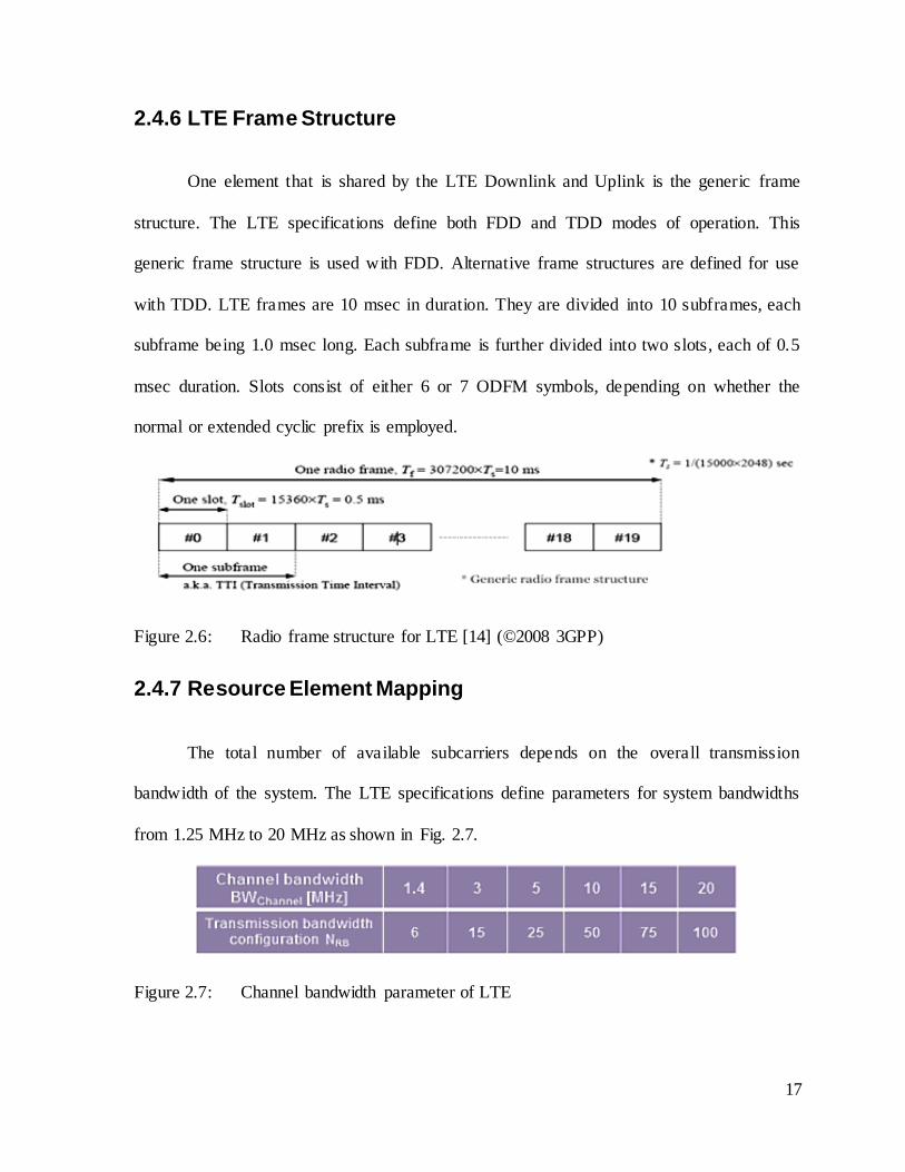
2.4.6 LTE Frame Structure
One element that is shared by the LTE Downlink and Uplink is the generic frame
structure. The LTE specifications define both FDD and TDD modes of operation. This
generic frame structure is used with FDD. Alternative frame structures are defined for use
with TDD. LTE frames are 10 msec in duration. They are divided into 10 subframes, each
subframe being 1.0 msec long. Each subframe is further divided into two slots, each of 0.5
msec duration. Slots consist of either 6 or 7 ODFM symbols, depending on whether the
normal or extended cyclic prefix is employed.
Figure 2.6: Radio frame structure for LTE [14] (©2008 3GPP)
2.4.7 Resource Element Mapping
The total number of available subcarriers depends on the overall transmission
bandwidth of the system. The LTE specifications define parameters for system bandwidths
from 1.25 MHz to 20 MHz as shown in Fig. 2.7.
Figure 2.7: Channel bandwidth parameter of LTE
18
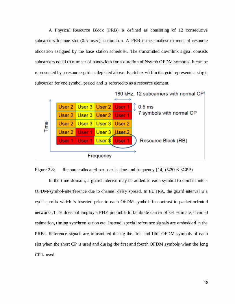
A Physical Resource Block (PRB) is defined as consisting of 12 consecutive
subcarriers for one slot (0.5 msec) in duration. A PRB is the smallest element of resource
allocation assigned by the base station scheduler. The transmitted downlink signal consists
subcarriers equal to number of bandwidth for a duration of Nsymb OFDM symbols. It can be
represented by a resource grid as depicted above. Each box within the grid represents a single
subcarrier for one symbol period and is referred to as a resource element.
Figure 2.8: Resource allocated per user in time and frequency [14] (©2008 3GPP)
In the time domain, a guard interval may be added to each symbol to combat inter-
OFDM-symbol-interference due to channel delay spread. In EUTRA, the guard interval is a
cyclic prefix which is inserted prior to each OFDM symbol. In contrast to packet-oriented
networks, LTE does not employ a PHY preamble to facilitate carrier offset estimate, channel
estimation, timing synchronization etc. Instead, special reference signals are embedded in the
PRBs. Reference signals are transmitted during the first and fifth OFDM symbols of each
slot when the short CP is used and during the first and fourth OFDM symbols when the long
CP is used.

19
2.4.8 Cell-Specific Reference Signals
In Rel-8, cell-specific Reference Signal (RS) are provided for 1, 2 or 4 antenna ports
• Pattern designed for effective channel estimation
• Sparse diamond pattern supports frequency-selective channels and high mobility with low
overhead
• Up to 6 cell-specific frequency shifts are configurable
• Power-boosting may be applied on the Resource Element (RE) used for RS
• QPSK sequence with low PAPR
2.4.9 OFDMA
LTE uses OFDMA for the downlink – that is, from the base station to the terminal
[14]. OFDMA meets the LTE requirement for spectrum flexibility and enables cost-efficient
solutions for very wide carriers with high peak rates. OFDM uses a large number of narrow
sub-carriers for multi-carrier transmission. The basic LTE downlink physical resource can be
seen as a time-frequency grid. In the frequency domain, the spacing between the subcarriers,
Δf, is 15kHz. In addition, the OFDM symbol duration time is 1/Δf + cyclic prefix. The cyc lic
prefix is used to maintain orthogonality between the sub-carriers even for a time-dispersive
radio channel. One resource element carries QPSK, 16QAM or 64QAM. With 64QAM, each
resource element carries six bits. The OFDMA symbols are grouped into resource blocks.
The resource blocks have a total size of 180kHz in the frequency domain and 0.5ms in the
time domain. Each 1ms Transmission Time Interval (TTI) consists of two slots (Tslot).
20
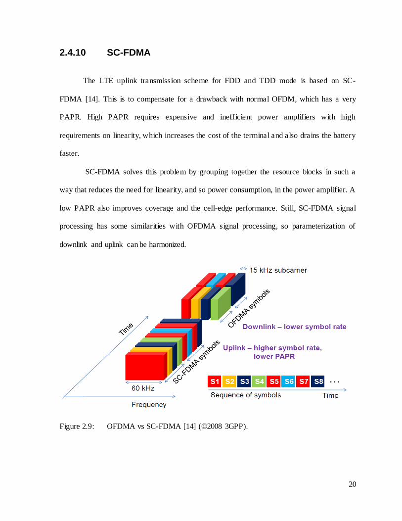
2.4.10 SC-FDMA
The LTE uplink transmission scheme for FDD and TDD mode is based on SC-
FDMA [14]. This is to compensate for a drawback with normal OFDM, which has a very
PAPR. High PAPR requires expensive and inefficient power amplifiers with high
requirements on linearity, which increases the cost of the terminal and also drains the battery
faster.
SC-FDMA solves this problem by grouping together the resource blocks in such a
way that reduces the need for linearity, and so power consumption, in the power amplifier. A
low PAPR also improves coverage and the cell-edge performance. Still, SC-FDMA signal
processing has some similarities with OFDMA signal processing, so parameterization of
downlink and uplink can be harmonized.
Figure 2.9: OFDMA vs SC-FDMA [14] (©2008 3GPP).

21
2.4.11 Downlink Physical Layer Procedures
During the cell search, the UE searches for a cell and determines the frame
synchronization of that cell. Scheduling is done in the base station (eNodeB). The downlink
physical control channel informs the users about their allocated time/frequency resources and
the transmission formats to use. The scheduler evaluates different types of information, e .g.
Quality of Service parameters, measurements from the UE, UE capabilities, buffer status.
Link adaptation is already known from HSDPA as Adaptive Modulation and Coding.
Also in E-UTRA, modulation and coding for the shared data channel is not fixed, but it is
adapted according to radio link quality. For this purpose, the UE regularly reports Channel
Quality Indications (CQI) to the eNodeB.
Downlink Hybrid Automatic Repeat request (ARQ) is also known from HSDPA. It is
a retransmission protocol. The UE can request retransmissions of incorrectly received data
packets. Acknowledge/Not Acknowledge (ACK/NACK) information is transmitted in uplink,
either on Physical Uplink Control Channel (PUCCH) or multiplexed within uplink data
transmission.
2.4.12 Uplink Physical Layer Procedures
The random access may be used to request initial access, as part of handover, or to re-
establish uplink synchronization. 3GPP defines a contention based and a non-contention
based random access procedure.
Scheduling of uplink resources is done by eNodeB. The eNodeB assigns certain
time/frequency resources to the UEs and informs UEs about transmission formats to use.
Scheduling grants for the uplink are communicated to the UEs via the Physical Downlink

22
Control Channel (PDCCH) in the downlink. The scheduling decisions may be based on
Quality of Service (QoS) parameters, UE buffer status, uplink channel quality measurements,
UE capabilities, UE measurement gaps, etc. As uplink link adaptation methods, transmission
power control, adaptive modulation and channel coding rate, as well as adaptive transmission
bandwidth can be used.
Uplink timing control is needed to time align the transmissions from different UEs
with the receiver window of the eNodeB. The eNodeB sends the appropriate timing-control
commands to the UEs in the downlink, commanding them to adapt their respective transmit
timing.
Uplink Hybrid ARQ protocol is already known from High-speed Uplink Packet
Access (HSUPA). The eNodeB has the capability to request retransmissions of incorrectly
received data packets. ACK/NACK information in downlink is sent on Physical Hybrid ARQ
Indicator Channel (PHICH).
2.4.13 Receiver UE Processing
OFDM receiver - undoes the unequal cyclic prefix lengths per OFDM symbol in a
slot and converts back to the time- and frequency-domain grid structure. MIMO receiver
subsystem which includes Channel Estimation employs least-squares estimation using
averaging over a subframe for noise reduct ion for the reference signals, and linear
interpolation over the subcarriers for the data elements. This uses the cell-specific RS signals
for the channel estimates. Codebook selection employs the MMSE criterion to calculate the
codebook index per subframe [15]. When the Enable PMI Feedback parameter is on, this
index is fed back to the transmitter for use at the next time step. Otherwise, the user-specified

23
codebook index is used for the duration of the simulation. The feedback granularity modeled
is once for the whole subframe (wideband) and applied to the next transmission subframe.
MIMO receiver employs a linear MMSE receiver to combat the interference from the
multiple antenna transmissions. Soft-decision demodulation is employed per codeword to
facilitate downstream turbo decoding.
2.5 LTE Advanced: Proposed Key Areas For Improvement
LTE-A is a standard in Mobile communication submitted to ITU-T in 2009. It was
approved by ITU and was finalized by 3GPP in March 2011 [16]. It is an extension of LTE
standard. There were some specific enhancements targeted for LTE-A over LTE. These are
as follows:
1. Data Rate And Spectral Efficiency
Increasing the peak data rate in Downlink to 3Gbps and Uplink 1.5Gbps.Higher spectral
efficiency, from a maximum of 16bps/Hz in R8 to 30 bps/Hz in R10.
2. Coverage Of Dead Zones And Interference Cancellation
With increase in cell phone users in last decade, congestion in cellular cell sites have
increased. Due to the inefficient radio resource reuse technology being used causing
interference between cells. It is getting difficult for the network operators to provide a good
QoS to customers. Moreover places like subways, sub-urban routes, tunnels have less
coverage and calls kept on getting dropped. These are called dead zones and vary from
carrier to carrier. LTE-A enhancements over LTE are targeted to mitigate dead zones.

24
3. Incorporating Legacy Systems
Different types of users use the network in a different way and for different applications.
Legacy systems like HSPA, HSDPA, GSM, CDMA, General Packet Radio Service (GPRS)
and Wireless Fidelity (WiFi) needs to be accomodated. So LTE-A should have backward
compatibility to all the systems.
4. Radio Spectrum Sensing Capabilities (Intelligent Networks)
In a few years from now, there will be an overlap of coverage between different radio
technologies, by the same operator within the same area and the handset or device has to be
intelligent enough to make the decision to use the Radio infrastructure. The device or handset
will have many radios built in and the software stack will have to make the decision based
not only on the received signal strength but the capacity limitations while moving seamlessly
between one another to be able to use the best QoS for the type of service used. For example
a browsing service will not be as data hungry as a video call or a YouTube video.
2.6 LTE Advance Techniques
2.6.1 Heterogeneous Networks
Since the radio link performance is fast approaching theoretical limits, the next
performance and capacity jump will come from an evolution of network topology in LTE-A
by using a mix of macro cells and small cells in a co-channel deployment. LTE-A HetNets
will use a mix of macro, pico, femto and radio-over-Fiber Connected base stations,
effectively bringing the network closer to the user. LTE-A HetNets will support Range
Expansion and Resource Partitioning with an Enhanced Inter Cell Interference Coordination
(eICIC) software upgrade to a LTE-R8 network. Range Expansion allows more user

25
terminals to benefit directly from low-power base stations. Adaptive inter-cell interference
coordination uses Almost-Blank Subframes to provide smart resource allocation amongst
interfering cells and improves inter-cell load balancing in heterogeneous networks. Advanced
terminal receivers cancel interference of legacy overhead channels in Almost-Blank
Subframes from interfering cells to enable full Range Expansion of low-power small cells.
2.6.2 Carrier Aggregation (CA)
CA is one of the key techniques in LTE-A to increase the system bandwidth thereby
increasing peak data rates. Since backward compatibility with rel 8 & 9 is required, the CA is
done with rel 8 & 9 carriers. In LTE-A aggregation is only allowed for five component
carriers (i.e., 1.4 MHz/3 MHz/5 MHz/10 MHz/15 MHz/20 MHz) till 20 MHz adding upto a
total of 100 MHz. There are three types of aggregations,
1. Intra-Band Contiguous CA
In this case, Contiguous bandwidth wider than 20 MHz is used. For example, wideband such
as 3.5 GHz band would fit this model.
2. Inter-Band Non-Contiguous CA
Non-contiguous band over multiple bands is used here. Network with two spectrum bands
(i.e., 2 GHz and 800 MHz) would fit this model. This scenario would have advantage on
having higher throughput simply by two carriers as well as the improvement on stable
transmission by two different spatial paths on different spectrum bands.

26
3. Intra-Band Non-Contiguous CA
Non-contiguous band in same band is used in this scenario. This model would fit
operators in North America or Europe, who have fragmental spectrum in one band or share
same cellular network.
Figure 2.10: Carrier aggregation [16] (©2011 3GPP)
Major Bottlenecks in implementation of CA:
The major design challenge is on terminal side. Support of higher bandwidths and
aggregation of carriers in different frequency bands increase complexity of transceiver
circuits, including component design like wideband power amplifiers, highly efficient
switches and tunable antenna elements.
The additional functionality provided to PHY/MAC layer and the adaptations to the
RRC layer need to be thoroughly tested.

27
2.6.3 Coordinated Multipoint (CoMP)
The signal strength is lost with increasing distance from base stations due to path loss
fading, shadowing and multipaths interference. Implementation of frequency reuse in 3G and
LTE was used to reduce the interference somewhat. But as the network grows in size and
more number of subscribers are present, there is increasing interference in the cells.
In [17] network coordination has been presented as an approach to mitigate intercell
interference and hence improve spectral efficiency. Fig. 2.11 shows the cooperation
architecture for CoMP. The same spectrum resources are used in all sectors, leading to
interference for terminals at the edge between the cells, where signals from multiple base
stations are received with similar signal power in the downlink.
Figure 2.11: Base station cooperation: intersite and intrasite CoMP. [17] (©2011 IEEE)

28
There are two types of CoMP structure possible. One is a decentralized control based
structure that involves multiple eNBs. The eNBs may be interconnected by the logical X2
interface. The other is a more centralized architecture with different remote antenna units
(RAU). The eNBs are connected to the central processor via optical fiber links.
The cooperation techniques aim to avoid or exploit interference in order to improve
the celledge and average data rates. CoMP can be applied both in the uplink and downlink.
All schemes come with the cost of increased demand on backhaul (high capacity and low
latency), higher complexity, increased synchronization require ments, more channel
estimation effort, more overhead, and so on.
2.6.4 Enhanced MIMO
LTE Rel.8 supported up to 4x4 MIMO multiplexing for downlink and nothing for
uplink. LTE-A supports single user MIMO scheme up to 8x8 MIMO for downlink and 4x4
MIMO for uplink. With this technology, it achieves peak spectral efficiency of 30 bit/s/Hz
for downlink and 15 bit/sec/Hz for uplink. In other words, single 20MHz bandwidth to
achieve up to 600Mbps downlink speed. Multi-user MIMO is also used to increase peak data
rate as well as the system capacity and cell edge user throughput. Various methods used in
Multi-user MIMO like dedicated downlink beamforming, adaptive transmission power
control, and multi cell simultaneous transmission help in increasing throughput of the system.

29
2.7 Cellular Architectures
2.7.1 Micro Base Station Architecture
Micro base stations are good at providing blanket coverage, especially with
techniques such as beam-forming, which adaptively directs radio signals toward receivers.
However, some areas will always present challenges: behind buildings and hills or inside
buildings. Studies have shown that poor performance in homes or offices is one of the top
reasons why people change cellular carriers. When cellular networks were first rolled out,
people accepted the fact that performance was poor in indoor environments. However, as end
users shift to using their mobile phone as their only voice device, demands for better
coverage have increased.
The exterior wall of any building can significantly degrade a wireless signal coming
from a macro base station. A common estimate of the amount of power lost through an
exterior wall is on the order of 9–15 dB (decibels). Since every 3 dB reduction represents
half of the power (based on the logarithmic decibel scale), 9–15 dB signal loss means that
only one eighth to one thirty-second of the power from the outside makes it inside.
Additional obstructions such as interior walls can easily degrade signal levels enough to
result in dropped calls and significantly reduced data rates.
Another factor that comes into play is the higher frequency bands used for broadband
wireless compared to traditional second-generation (2G) voice solutions. Typically the higher
frequencies have even more difficulty penetrating exterior walls when operating at
comparable power levels. In the face of these difficulties, the demand for bandwidth
continues to increase. Users want to send and receive virtually any type of media from

30
virtually any location, so Worldwide Interoperability for Microwave Access (WiMAX)
networks need to ensure high data rates over their entire coverage areas. The cost of
delivering this coverage can be high if a network uses only macro base stations. The
equipment and the backhaul to support it is particularly expensive due to high-performance,
carrier-class features such as redundancy, hot-swap capability, high-power radios, and
support for thousands of users.
Deploying many micro base stations is thus a costly way to solve coverage issues,
and in some situations, even a single micro base station is too expensive. In developing
countries where average revenue per user is around $10 or less, the cost of the micro base
station becomes a barrier to a profitable business model. To solve the challenges of macro
base stations, often micro base stations provide a suitable solution. Micro base stations [18]
typically consist of a small rack-mounted device with a tower mounted radio. The radios
typically connect to the rack via an optical cable using Open Base Station Architecture
Initiative (OBSAI) or Common Public Radio Interface (CPRI) standards. These base stations
do not have the carrier-class features of a macro base station and hence are significantly less
expensive. Most of the deployments for these base stations are in developing countries or
deployments using unlicensed spectrum, where access is otherwise nonexistent and
customers are unwilling to pay high average revenue per users. Typically, each micro base
station supports three sectors, with hundreds of users per sector. To reduce costs, the radio
power is not as high as that of a macro base station.

31
2.7.2 Femtocell Architecture
With different cellular telecommunications systems there will need to be different
ways of implementing the actual femtocell network architecture. However there are a number
of common requirements for the femtocell network architecture regardless of the cellular
system used. 3GPP worked with vendors, and operators to provide the optimum standard.
The new standard developed a new interface and also standardized the elements within the
femtocell network architecture.
3GPP HeNB Femtocell System Architecture
There are three main elements to the femtocell network architecture [19] as defined by 3GPP
are Home NodeB (HeNB), HeNB Gateway (HeNB-GW) & Iu Interface. The Fig. 2.12 shows
the femtocell architecture.
1. Home NodeB
The Home Node B is 3G UMTS terminology for the femtocell access point within the home,
or other location. The HeNB will incorporate the capabilities of a standard Node B as well as
the radio resource management functions found within a Radio Network Controller, RNC.

32
Figure 2.12: Femto cell architecture [5] (©2011 IEEE)
2. HeNB Gateway (HeNB-GW)
This is the entry point to the core network. The link into the core network is provided over
Iu-cs and Iu-ps interface which are already used for links from Radio Network Controllers to
the remaining core network.
The HNB-GW has the following functions:
It provides authentication and certification to allow only data to and from authorized
HeNBs
The HeNB-GW aggregates traffic from a large number of HeNBs and provides an
entry point into the operator core network.
The HeNB-GW provides a mechanism to support enhanced features such as clock
sync distribution, other IP based synchronization (e.g. IEEE1588)

33
3. Iu Interface
The Iu-h interface is used to provide the link or interface that connects the HeNB with the
HeNB-GW. The Iu interface used here is a commercially available co-axial link. The Iu
interface includes a new HeNB Application Protocol, HeNBAP that provides the high level
of scalability required for the HeNB deployment that will occur in a rather ad-hoc fashion.
2.7.3 Broadband Radio Over Fiber Distributed Antenna System
Architecture
Fig. 2.13 shows the Broadband ROF Distributed Antenna System architecture
comprise of three main components: distributed antenna system (access nodes), central
processing facility and fiber connection medium linking the antenna sub-system and the
central processing facility. The preceding sections elaborate in detail the each of the
component.
1. Distributed Antenna System
In a typical Distributed Antenna Systems (DAS) system the access nodes provide a
convenient means of delivering blanket coverage for a targeted area, while avoiding the time
consuming and costly cell planning phases. All the processing for the access nodes is done at
the central processing entity. The access nodes are merely a distributed set of antenna
elements. Our architecture uses the fast and reliable fiber connection medium to/from the
central processing entity. Therefore the DAS has the potential to scale from a few antenna
elements, covering tens of square meters of space, to tens of antenna elements covering a few
square kilometers of the targeted area.

34
Figure 2.13: Broadband radio over fiber distributed antenna system architecture [5]
(©2011 IEEE)
Similar to traditional two-tier networks, the location arrangement of individual
antenna elements in this massive DAS is quite arbitrary, providing ease of deployment. Due
to the coordination capability of Broadband ROF Distributed Antenna System, however, a
much more efficient interference management strategy than traditional femtocell networks
can be achieved in the proposed system. For instance, UMTS LTE standard supports a
cooperative mode of operation between macrocells, named CoMP transmission. However,
due to the independent operation of femto- and picocells, and lack of interaction
infrastructure in the second tier of the network, coordination of transmissions to/from HeNBs
is not possible. On the other hand, Broadband ROF Distributed Antenna System facilitates

35
coordinated transmission/reception schemes not only at the macro level but also in the femto-
and pico cell tier.
2. Central Processing Facility
The central processing facility is the core of any DAS architecture. All the processing of the
signals/data are done at the central processing entity, which provides several operational
flexibility to enhance the system performance. The resource allocation decision making in
each femto- and picocell associated with any given antenna element will be made in harmony
with neighboring cells. Several studies [5] have indicated that availability of the high-end
central processing entity in the DAS architecture immensely improves the resource
utilization across the networks and a lower interference level, which yields better system
performance.
Furthermore, by centralizing the resource allocation significantly reduces the
signaling overhead associated with coordination transmission and reception of data, such as
through employing CoMP in the LTE context. In effect, Broadband ROF Distributed
Antenna System realizes a distributed architecture with centralized decision making
capabilities.
3. Fiber Connected Medium
We predominantly use fiber optic cables connecting the central processing entity to each
antenna element. The inexpensive optical fiber backbone network operational advantages
such as large bandwidth, immunity to electromagnetic interference, low power usage.
First, a mechanism for electrical-to-optical conversion and vice versa is in charge of
transforming the communicated signal over various sections of the Broadband ROF
Distributed Antenna System according to their medium requirements. This scheme is known

36
as RoF in the literature [20]. Unlike wireline network counterparts, such as the Ethernet, the
conveyed signal will remain analog, as opposed to digital, over the fiber connection medium.
Several proof-of-concept demonstrations, mainly focusing on WLAN over fiber
communications, have been reported in the literature [21].
Second, the optical links will form a network that can utilize passive or active optical
networking protocols. A passive optical network (PON) is a more cost-efficient
implementation, which employs one pair of optical fibers for duplex transmissions between
an antenna element and the central processing entity. In the simplest case, each access node
employs different set of transmit and receive antennas connected via power and low-noise
amplifiers to the respective fibers. The transmission/reception of signals from/to each
antenna element is then controlled based on a time-division multiplexing (TDM) scheme. If
there are multiple set of transmit/receive antennas at each access node & multiple antenna
elements are fed via a shared pair of optical fibers, wavelength-division multiplexing (WDM)
techniques can further be exploited [22].
2.8 Wavelets in Wireless Communications
The idea of using wavelet transform instead of Fourier was introduced a decade ago
[23] [24]. However, such alternative methods have not been foreseen as of major interest
and therefore have received little attention. With the current demand for high performance in
wireless communication systems and limitations of Fourier based OFDM systems as
highlighted in section 2.5, it is imperative to look for better alternatives.
Wavelet theory has been foreseen by several authors as a good platform on which to
build multicarrier waveform bases [25], [26], and [27]. Wavelet packet bases therefore

37
appear to be a more logical choice for building orthogonal waveform sets usable in
communication. In their review on the use of orthogonal transmultiplexers in
communications [23], Akansu et al. emphasize the relation between filter banks and
transmultiplexer theory and predict that wavelet packet modulation has a role to play in
future communication systems. In this section, we will briefly describe the different studies
based on wavelets which provide viable solutions to drawbacks of current wireless systems.
2.8.1 Flexibility Of Orthogonal Wavelet System
In OFDM, the discrete waveforms are the well-known M complex basis functions
w[t]*exp(j*2Π*(m/M)*kT) limited in the time domain by the window function w[t]. The
corresponding sine-shaped waveforms are equally spaced in the frequency domain, each
having a bandwidth of 2Π/M and are usually grouped in pairs of similar central frequency
and modulated by a complex encoded symbol. Whereas wavelets produce orthogonal
waveforms that are distributed both in time and frequency domain. Due to the wavelet
transform containing not only frequency information but time information as well, it is now
possible to effectively convey higher data rates within each subband where the only limit is
the trade-off between the subband resolution in the time and frequency domain – ie the
higher the frequency resolution, the lower the time resolution and vice versa. In wavelet
multiplexing, the bandwidth, BWk, of each subband, k, can be calculated from to total
bandwidth, BW [28]
/ 2 ,1
/ 2 ,k n 1
k
k n
BW k nBW
BW
Where n is the number of levels. The number of samples per subband, Nk, can be
calculated from the efficiency of the channel, N
(2.1)

38
/ 2 ,1
/ 2 ,k n 1
k
k n
N k nN
N
From above, it is observed that the bit rate per subchannel depends on the number of
levels of decomposition and that the larger the number of subchannels, the smaller the
bandwidth of each channel and thus the lower the maximum possible bitrate through each
channel. Because of this there is an inherent flexibility in the system which means that the
signal can be optimized for a specific application and channel conditions.
2.8.2 Wavelet Based Downlink Scheduling In LTE Systems
A study and performance evaluation has been done to provide downlink scheduling in
LTE cellular systems [29]. It proposes the use of wavelet transform in LTE cellular systems.
Mathematical expressions have been derived to represent data rate in LTE downlink
transmission based on Wavelet and Fourier Transforms. Furthermore, a comparison between
these two systems is provided for QPSK, 16-QAM and 64-QAM modulation. Simulation
results show that the proposed OWDM approach outperforms the traditional OFDM systems
in BER versus SNR comparison. It also shows that the data rate can also be increased by the
amount of Cyclic Prefix/Symbol Time%, as there is no need for a channel prefix in an
OWDM-based system.
2.8.3 Wavelet Based PAPR Reduction In OFDMA Systems
Wavelet based pre-processing technique has been shown to reduce the PAPR problem
of OFDMA systems [30]. A new technique has been introduced in [30] to increase
orthogonality among data which is based on imposing the eigenvalue extraction features. The
(2.2)

39
simulation showed upto 60% lower PAPR values as compared to conventional OFDMA
systems even in condensed multipath channel. This was achieved by increased complexity at
the transceiver structure.
2.8.4 Low Complexity In Wavelet Based System As Compared To
OFDMA
There is no limitation in number of subcarriers in orthogonal Wavelet modulation
unlike OFDM, where they are usually fixed at the time of design and is difficult to
implement a FFT transform of a programmable size. In wavelets the transform size is
exponentially dependent on the number of iteration of the algorithm [31]. So it is easy to
configure them without increasing overall complexity in implementation. So this allows the
change of transform on the fly.
2.8.5 Wavelet Based Multi Carrier Multiple Access Scheme For
Cognitive Radio
The system exploits the multicarrier feature of wavelet transform and multiple access
features of OFDMA. A modified algorithm is described for free channel assignment in
Cognitive Radios. The simulation results show that BER performance is better compared to
that of OFDMA system. The degradation in frequency and timing offset is similar to that of
OFDMA [32].
Analyzing the approaches described above gives insight about the extensive research
performed on the various solution approaches to problems of LTE OFDMA systems and
provides proof that orthogonal wavelets are a better and viable alternative to the existing
40
wireless systems. Although the analysis and evaluations were done for BER, PAPR,
Throughput, the above literature lacks in a unified system implementation, resource analysis
and thorough performance evaluation for current LTE systems. Our major contribution in
this thesis is to deal with these shortcomings in the present knowledge and present an overall
system level solution.
2.9 Literature Review Of MIMO-LTE Matrix Inversion
Algorithms
For MIMO-LTE matrix inversion, the size of matrix is larger than 2x2 in fixed- point
implementation. Fixed-point algorithm has poor stability but floating-point work well and
computation time requires fewer cycles. Floating point approach gives better stability,
accuracy and resolution to the decoded data resulting in better BER.
Methods for computing matrix inversion can be divided into two categories: iterative
and direct. Iterative methods require an initial estimate of the solution and subsequent
updates based on calculation of the previous estimate error. Normally, these iterative
methods involve high-complexity sequential matrix computations and are not particularly
suitable for real-time implementation. QRD is an attractive approach for matrix inversion due
to its well-known numerical stability [33]. Several algorithms and architectures have been
proposed for the computation of QRD-based matrix inversion; those which employ the
Gram-Schmidt [34] and conventional Givens rotations algorithms are disadvantaged from an
implementation perspective as they require high-complexity square-root operations. Whilst
the shift-and-add processing nature of Coordinate Rotation Digital Computer (CORDIC)-
based matrix inversion [35] offers low complexity hardware implementation, its inherent

41
latency can preclude it from high-performance applications. Squared Givens rotations (SGR)
offer square-root free processing and a number of SGR-based matrix inversion architectures
have been proposed [36], [37], [38]. These algorithms suffer from high level of
computational complexity and are difficult to implement in real time systems.
2.10 Summary
Apart from the pros of LTE compared to previous 2G & 3G legacy networks, it has
cons that lead to the development of LTE-A with the aim of resolving these issues. The
major disadvantages are:
Size of FFT in OFDM increase with order of modulation scheme like 1024-
QAM.
High PAPR and high Inter carrier interference in OFDM.
Large MIMO required for high data rate but complexity of channel estimation
and decoder increases exponentially.
Downlink and uplink use separate architectures. SC-FDMA is used in uplink
to reduce power consumption and high PAPR problem in OFDMA.
Blackout of signal in tunnels and subways. Coverage not sufficient to provide
optimum Quality of Service.
Flexibility of resource allocation is not there according to user demands and
channel conditions.
LTE-A systems use the existing OFDMA architecture in downlink. Moreover,
implementation of heterogeneous networks requires adaptable architecture which OFDMA
does not suffice. Coordinated multipoint architecture can help reduce the CAPEX and

42
latency in the system but it requires a centralized architecture for that purpose. Enhanced
MIMO with multiple antennas needs better channel estimation strategies and good bit
resolution of ADC‟s and DAC‟s. Thus in the following chapters we propose and prove by
graphs and plots new algorithms to contribute towards the development of new LTE
architecture.

43
Chapter 3
A Orthogonal Wavelet Division
Multiple Access Processor
Architecture For LTE-A Radio-Over-
Fiber HetNet Systems
This chapter gives a detailed formulation of the OWDMA architecture. We develop the
architecture, synthesize it and compare it with state of the art techniques.
3.1 Overview Of OWDMA
OWDMA has been proposed as a viable alternative to OFDMA in communication
systems. Linfoot et al. [28], [39] demonstrated that OWDMA could be an effective
alternative to OFDMA. But their work concentrated on digital video broadcast and results
were only plotted for the BPSK modulation scheme. Raajan et al. [40] provided BER
performance graphs for all the wavelets and modulation schemes, but no hardware
architecture was provided for the proposed system. Similarly, Tao et al. [41] and Liew et al.

44
[42] analyzed orthogonal wavelet division multiplexing for signaling over wideband linear
time-varying channels but again did not provide any architecture for deployment. 1-D
orthogonal wavelets have been used and elaborated [43] - [47] for image processing
applications.
In the conference article [1], a sequential output-based parallel processing (SBPP)
architecture for OWDM was proposed and evaluated for BER and PAPR. The deployment in
LTE-A ROF future 3GPP rel 10 and above requires that its structure should be flexible
enough to adapt to different values of transform size according to channel conditions in order
to service uniformly the same number of users. The structure needs to accommodate both
forward and inverse operations through a common control input. The architecture should be
power efficient, be easily controllable through a single control, and should have input-output
ports matching to other system sub-blocks that will satisfy the timing requirements of the
whole system. Moreover, it is important for it to offer improved performance in terms of
spectral efficiency (throughput), quality of service (better BER at the same SNR) and should
fit well in Radio-over-Fiber systems. An OWDMA architecture is developed in this chapter
that can achieve significantly better performance, is easy to deploy, and consumes fewer
resources than any similar architecture available in the literature.
3.2 Orthogonal Wavelet Division Multiplexing
Fast fluctuations in the time domain or frequency-specific information in the time
domain can only be revealed through a time/frequency analysis. The wavelet transform maps
a time function into a two-dimensional function of „a‟ (the scale) and „τ‟ (the translation) of

45
the Wavelet function along the time axis [48], [49]. The continuous waveform transform
(CWT) of a signal s(t) has been defined as
t1
CWT a, s t dtaa
(3.1)
where t is the time, ψ(t) is the basic (or mother wavelet) and ψ((t − τ)/ a) is the
translated baby wavelet [28] created by either stretching or compressing the mother wavelet.
3.2.1 Formulation Of OWDM From The 9/7- Filter Using Lifting
From the CWT, it is possible to construct the discrete wavelet transform (DWT) and
the inverse DWT) from banks of matched high pass and low pass filters [50]. Single carrier
systems tend to have high bit rates but low frequency resolution, whereas OFDM has many
sublevels, each transferring at a low bit rate. Since the wavelet transform contains both time
and frequency information, it is possible to effectively send different data rates in different
sublevels, according to channel conditions. When considering the DWT, there are a number
of mother wavelet families that need to be evaluated. It was realized that only three families
of wavelet should be considered: Daubechies, Symlet, and Coiflet [51]. To replace OFDM
systems in a multipath environment having carrier and symbol interference, the wavelets
needs to be orthogonal and periodical. Realization using discrete structures is also important
for purpose of implementation.

46
Figure 3.1: Signal to noise ratio versus bit error rate comparison for various
orthogonal wavelet families. [51] (©2008 IEEE)
Fig. 3.1 presents a comparison of signal to noise ratio vs. bit error rates for the Symlet
1, Coiflet 2, and Daubechies 2 similar-order filters [51]. It can be seen that the least resilient
wavelet family is the Symlet, followed by the Coiflet, then the Daubechies, which appear to
be better suited for implementation.
The lifting scheme is used for the development of the architecture for a 9/7
Daubechies 1-D wavelet filter with two stages of lifting (N=2), i.e., predict1 and update1,
folllowed by predict2 and update2 in a second stage, followed by scaling [31], [52]. The
basic idea of the lifting scheme is first to compute a trivial wavelet (or lazy wavelet transform)
by splitting the original 1-D signal into odd- and even-indexed subsequences and then
modify their values using alternating prediction and updating steps. The lifting algorithm
consists of the following three steps.

47
1. Split Step
The original signal, X(n), is split into odd and even samples (lazy wavelet transform).
2. Lifting Step
This step is executed as N sub-steps (depending on the type of the filter), where the
odd and even samples are filtered by the prediction and update filters.
3. Scaling Step
After N lifting steps, scaling coefficients K and 1/K are applied respectively on the odd
and even samples in order to obtain the low-pass band and the high-pass sub-band.
OWDMA is a system, in which the wavelet domain is used to separate the sub-band
components in the same way as OFDMA. The big difference between OFDMA and
OWDMA is that in OFDMA the FFT performs sub-band decomposition with a specific
number of sub-bands at well-defined intervals, while OWDMA may dynamically allocate the
number of sub-bands and the bandwidth of each [53].
3.2.2 Sequential Output-Based Parallel Processing Architecture For
OWDM
The SBPP architecture [1] that forms the basis for our proposed OWDMA
architecture is described next. The SBPP architecture is formed using a 9/7 bi-orthogonal
filter using a 2-stage lifting scheme. The system is designed to perform a series of sequential
operations – predict and update level 1, predict and update level 2, followed by scaling. The
OWDM block consists of two predict & update blocks and two scaling blocks. In the
transmitter, N complex symbols from the output of symbol mapper are fed to the input of the

48
OWDM modulator. The predict-and-update level 1 & 2 and the scaling operations are as
follows.
1. Predict & Update Level 1 & 2
All odd and even symbols can be computed in parallel blocks, except for the 1st, (2L-1)
th and
2Lth
symbols, based on Eqn. (3.2)-(3.6). Here M is the level of predict & update and varies
from 0 to 1. Li=1,2,..,N/2 (N-size of OWDM) and a & b are the coefficients as derived in [54]
when 9/7 biorthogonal lifting scheme is formulated from FIR (finite impulse response) filter
banks and c = a*b. Input from the first predict and update block is fed to the next one, thus
making the second block dependent on the first.
M 1 M M M M M MX 1 X 1 2 b X 2 2 c X 1 X 3
(3.2)
M 1 M M M M
i i i iX 2L X 2L a X 2L 1 X 2L 1
(3.3)
M 1 M M M M
i i i i
M M M M
i i i
X 2L 1 X 2L 1 b X 2L X 2L 2
c X 2L 1 2 X 2L 1 X 2L 3
(3.4)
M 1 M M M M
M M M
X 2L 1 X 2L 1 b X 2L X 2L 2
c X 2L 1 X 2L 3
(3.5)
M 1 M M MX 2L X 2L 2 a X 2L 1
(3.6)
0 1
0 1
0 1
a = -1.5861, a = 0.8829,
b = -0.05298, b = -0.44351,
c = 0.08403, c = -0.3916

49
2. Scaling
Finally, the output of the predict-and-update level 2 block is fed to the scaling block. Scaling
coefficients K (=1.149604398) [52], [53] and 1/K are applied respectively to the odd and
even samples in order to obtain the wavelet coefficients WC.
M 1
C i iW 2L X 2L K
(3.7)
M 1
C i i
1W 2L 1 X 2L 1
K
(3.8)
3.3 Proposed OWDMA Processor Architecture For LTE A-
ROF Layer 1
From the SBPP-OWDM scheme presented in the previous section, it is found that the
final scaling and dilation coefficients are interdependent on predict and update outputs at
each stage, thus there is a delay and it also affects throughput. The structure requires two
update and predict blocks to be implemented. OWDMA scheme requires that the structure
should be flexible enough to adapt to different values of N according to the channel
conditions. The structure needs to accommodate both forward and inverse operations through
a common control. The multiplicative coefficients for the filter need to be stored in a
hardware friendly format that will reduce the number of multiplication operations. Thus a
new OWDMA processor architecture have been developed that caters to all the requirements
of a multiple access system mentioned above. Moreover parallelism is exploited in the

50
architecture along with pipelining to formulate an efficient, low power and resource friendly
processor system.
Using Eqn. (3.2)-(3.8) predict and update block1 and predict and update block 2 are
combined together along with the scaling. In the forward operation, the wavelet coefficients
for odd and even samples are calculated using Eqn. (3.9)-(3.10). The odd values are
calculated using a structure implementing a 9-tap FIR (finite impulse response) filter and the
even values are found out with a 7-tap FIR filter structure as shown in Fig. 3.2. Odd value
wavelet coefficients 1st, 3
rd, (n-3)
rd & (n-1)
st and even value wavelet coefficients 2
nd , (n-2)
nd
& nth
have adjusted input values fed using the symmetry property of the filter. The values of
k before the first value „X[1]‟ and after the last value „X[N]‟ are replaced by their symmetric
values by using x[k] = x[k+2i], where i takes the value –k+1 w.r.t to the inputs index k in the
left side of the axis and it takes the value n-k at the right side of the axis. The FOC(j) & FEC(l)
are forward odd and even filter coefficients respectively where j=1,2…9 and l=1,2….7.
C C C C
V
C C C
E EN
FE 1 X N 3 FE 2 X N 2 FE 3 X N 1 FE 4 X N
FE 5 X N 1 FE 6 X N 2 FE 7 X N 3 ; N EVEN
Y N
(3.9)
C C C
C C C
C C C
ODD
FO 1 X N 4 FO 2 X N 3 FO 3 X N 2
FO 4 X N 1 FO 5 X N FO 6 X N 1
FO 7 X N 2 FO 8 X N 3 FO 9 X N 4 ; N
Y
D
N
O D
(3.10)

51
Figure 3.2: The core filter unit showing 9-tap and 7-tap FIR filter structure with input
X[N].
In the inverse operation, the wavelet coefficients for odd and even samples are
calculated using Eqn. (3.11)-(3.12). The odd values are calculated using a structure
implementing a 7-tap FIR filter and the even values are found out with a 9-tap FIR filter
structure. Odd value wavelet coefficients 1st
,3rd
& n-1th
and even value wavelet coefficients
2nd
,4th
, n-2th
& nth
have adjusted input values from symmetry in a similar way as described
in previous paragraph for the forward operation. The boundary conditions are formulated
using a state machine control logic implementation elaborated in control unit section. The
IOC(l) & IEC(j) are inverse odd and even filter coefficients respective ly where j=1,2…9 and
l=1,2….7.
FOC(1)
D D D D D D D D
Parallel To
Serial Wavelet Coefficients Input X[N]
FOC(9) FOC(8) FOC(7) FOC(6) FOC(5) FOC(4) FOC(3) FOC(2)
FEC(7) FEC(6) FEC(5) FEC(4) FEC(3) FEC(2) FEC(1)
YODD[N]
YEVEN[N]

52
C C C
C C C
C C C
EVEN
IE 1 Y N 4 IE 2 Y N 3 IE 3 Y N 2
IE 4 Y N 1 IE 5 Y N IE 6 Y N 1
IE 7 Y N 2 IE 8 Y N 3 IE 9 Y N 4 ; N EVEN
X N
(3.11)
C C C C
C C C
ODD
IO 1 Y N 3 IO 2 Y N 2 IO 3 Y N 1 IO 4 Y N
IO 5 Y N 1 IO 6 Y N 2 IO 7 Y N 3 ; N ODD
X N
(3.12)
The proposed OWDMA processor consists of a core unit to multiply filter
coefficients with delayed input and accumulate with previous value and compute the wavelet
coefficients. It has a control unit that controls which coefficients are to be applied at the
complex multiplier input and has a coefficient generator unit that reads the appropriate
coefficients from memory. The OWDMA unit acts as the slave to a master Scheduler unit
that feeds it with clock, address and input data and variables. Fig. 3.3 shows the high level
Very Large Scale Integration (VLSI) architecture of the OWDMA processor unit with the
scheduler. The architecture is 2-parallel structure due to simultaneous calculation of odd and
even data. The Scheduler and the three major units of the proposed system core unit, control
unit and the coefficient generator unit are discussed below.

53
Figure 3.3: The top level Generic OWDMA processor implementation block diagram.
WC
CLK
START
BUSY
D_REQ
ACK/ NACK
RST
N_OWDM
FW/ INV
CLK
CLK_EN
IN_EN
G1_EN
G2_EN
FW/INV
D_IN
C CFO IE C CFE IO
YODD
YEVEN
OUT_EN
SCHEDULER
CONTROL UNIT
CORE UNIT (FILTERS)
PARALLEL TO
SERIAL
COEFFICIENT GENERATOR COEFF_EN
OUT_EN
ADDRESS

54
3.3.1 Scheduler
The proposed OWDMA processor can be interfaced with the scheduler according to
the scheme presented Fig. 3.3. In this scheme the scheduler communicate with the OWDMA
processor using a set of dedicated hand-shake signals. The scheduler acts as the master, sets
the address of the processor and provide clock to it (CLK). First the scheduler requests the
control unit block to initiate a new transform using the START signal. The controller unit
sets the BUSY signal low if it is ready to start the process for the new transform or high if it
is in the middle of an already continuing process. When the controller is ready it sends a data
request (D_REQ) signal to the scheduler which then responds with the input data. If the
controller correctly gets the input, it sends an acknowledgement (ACK) signal otherwise it
sends NACKand the scheduler retransmits. Along with the data input it sends the information
for the size of OWDM (N_OWDM) as well as the forward/inverse operation ( FW INV ) signal.
The OWDMA processor uses the RST signal to indicate the end of data when it completes
the transform. At the same time it sets the BUSY signal low to indicate to the scheduler that
it is ready to start a new transform.
3.3.2 Core Unit
The core unit consists of two FIR filter units. One is 9-tap and the other is a 7-tap as
shown in Fig. 3.2. They both have CLK, CLK_EN, IN_EN, G1_EN, G2_EN, D_IN, and
FW INV as common inputs and YODD & YEVEN as the odd and even filter output. The only
difference is the inputted coefficients for the Multiply & Accumulate units inside the FIR
filters. The FOC (1…9), IEC (1…9) are coefficients inputs for the 9-tap filter block and FEC
(1…7), IOC (1…7) are coefficients inputs for the 7-tap filter block. These coefficients are

55
explained in more detail in the Section D. The CLK input counts from 0 to N+4 and then gets
reset. The extra 5 clock cycles after the normal N-cycles are for flushing the output to 0.
D_IN is the data input. IN_EN is enable signal for data input. G1_EN and G2_EN are enable
signal for switches that switch input gates and are enabled by the control logic. FW INV signal
is for forward (a „0‟) and inverse operation (a „1‟). The outputs of both the filters are fed to a
Parallel to serial converter block that down samples the data and rearranges the coefficients
to give the final coefficients WC. It has an OUT_EN (output enable) signal to start calculating
the output WC (the wavelet coefficients). Fig. 3.4 shows all the logic signals in a timing
diagram.
Figure 3.4: Timing diagram showing logical signals with clock.

56
3.3.3 Control Unit
The control unit consists of two separate logic units for forward and inverse
computation and is implemented using a finite state machine having 5 states S0, S1, S2, S3
and S4 respectively. It toggles on the positive CLK edge input and at each state the output
controls IN_EN, G1_EN, G2_EN, OUT_EN, FW/ INV _COEF_EN (0/1) and FW INV . The
FW INVsignal controls which control logic unit to be used (forward or inverse). G1_EN and
G2_EN are gate control switches that switch input for the delay registers at the boundary
conditions.
Figure 3.5: Symmetric boundary extension of input data
The input value has to be symmetrically extended at the boundaries to avoid
distortion. „X[1]‟ is the first input value and no previous value is available. Using the
symmetric property of the lifting scheme [54] as shown in Fig. 5, the next input value „X[2]‟
is extended to left of „X[1]‟ and is used to perform the filter operation. Similarly, at the end
of the row, the input value „X[N]‟ is the last one. By copying the input value „X[N-1]‟ to the
right of „X[N]‟ the boundary condition at the right end can be satisfied. The control logic is
shown in Fig. 3.6. At the positive edge count value of 4, G1_EN is enabled for one clock

57
cycle. G2_EN is enabled at nth
clock value. Output is calculated starting from 5th
clock count
to (n+4)th
count and then everything resets back to state S0.
Figure 3.6: Control logic finite state machine implementation
3.3.4 Coefficient Generator Unit
The coefficient generator block is a memory block that contains the odd and even
filter coefficients to be multiplied during forward/inverse operation with the filters.
Providing the appropriate constant to the multiplier, implements the desired multiplication.
The width of the multipliers is determined by the accuracy of the constants and the data path
bit-width. The drawback of the above implementation is that the multipliers occupy a great
amount of area and restrict the throughput of the processing unit. Using shift-add operations
S0 IN_EN=1
G1_EN=0
G2_EN=0
OUT_EN=0
FW / INV X S1
IN_EN=1
G1_EN=1
G2_EN=0
OUT_EN=0
FW / INV X
S2
IN_EN=1
G1_EN=0
G2_EN=0
OUT_EN=1
FW / INV X
S3 IN_EN=0
G1_EN=0
G2_EN=1
OUT_EN=1
FW / INV X
S4 IN_EN=0
G1_EN=0
G2_EN=0
OUT_EN=1
FW / INV X
4th
Clock Cycle (N+4)th
Clock Cycle
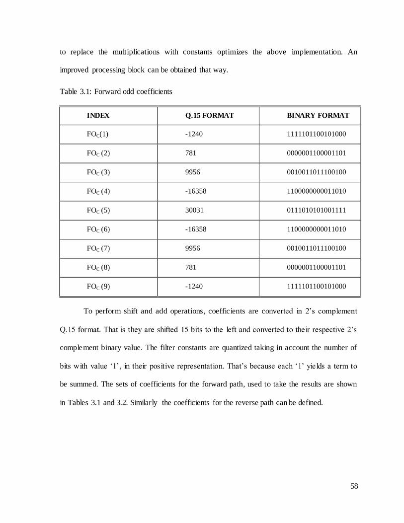
58
to replace the multiplications with constants optimizes the above implementation. An
improved processing block can be obtained that way.
Table 3.1: Forward odd coefficients
INDEX Q.15 FORMAT BINARY FORMAT
FOC(1) -1240 1111101100101000
FOC (2) 781 0000001100001101
FOC (3) 9956 0010011011100100
FOC (4) -16358 1100000000011010
FOC (5) 30031 0111010101001111
FOC (6) -16358 1100000000011010
FOC (7) 9956 0010011011100100
FOC (8) 781 0000001100001101
FOC (9) -1240 1111101100101000
To perform shift and add operations, coefficients are converted in 2‟s complement
Q.15 format. That is they are shifted 15 bits to the left and converted to their respective 2‟s
complement binary value. The filter constants are quantized taking in account the number of
bits with value „1‟, in their positive representation. That‟s because each „1‟ yields a term to
be summed. The sets of coefficients for the forward path, used to take the results are shown
in Tables 3.1 and 3.2. Similarly the coefficients for the reverse path can be defined.

59
Table 3.2: Forward even coefficients
INDEX Q.15 FORMAT BINARY FORMAT
FEC (1) 2115 0000100001000011
FEC (2) -1333 1111101011001011
FEC (3) -13700 1100101001111100
FEC (4) 25837 0110010011101101
FEC (5) -13700 1100101001111100
FEC (6) -1333 1111101011001011
FEC (7) 2115 0000100001000011
3.4 Pipelining The Parallel Architecture For Low Power
In the downlink and especially uplink of a LTE A-ROF network, power dissipation is
a major drawback of the system. So, architecture with low-power utilization is very much
beneficial. The extra power saved can be used to accommodate more number of users or
increase the range of the system. In the proposed OWDMA Processor Architecture,
pipelining the stages of the 9-tap and 7-tap filters along with the 2-stage parallel structure can
help save in power budget. P ipelining reduces the effective critical path by introducing
pipelining latches along the critical data path. The critical path (or the minimum time
required for processing a new sample) is limited by 1 multiply and 8 add times in 9-tap filter
structure and 1 multiply and 6 add times in 7-tap filter structure of OWDMA processor
respectively as shown in Fig. 3.2. Thus, the “sample period” is given by Eqn. (3.13)-(3.14)
where Tsample (9-tap) and Tsample (7-tap) are the sampling frequency of respective filters:

60
Sample M AT 9 tap T 8 T
(3.13)
Sample M AT 7 tap T 6 T
(3.14)
The pipelined implementation is done by introducing 14 & 10 additional latches in
the feed-forward path of the 9-tap and 7-tap filter structure respectively, thereby reducing the
critical path to TM+TA for both the filters. In an M-level pipelined system, the number of
delay elements in any path from input to output is (M-1) greater than that in the same path in
the original sequential circuit. Thus we apply 8-level pipelining to the 9-tap filter circuit and
a 6-level pipelining to the 7-tap filter circuit respectively. When sample speed does not need
to be increased, this can be used for lowering the power consumption in the RTL. The power
dissipation (PCMOS) in any circuit depends on the total capacitance Ctotal of the
Complementary Metal Oxide Semiconductor (CMOS) logic, the supply voltage VCC and the
clock frequency f.
2
CMOS total CC seqP C V f ,f 1 T
(3.15)
We define another parameter here called the propagation delay (Tpd) of the circuit.
From [55], we found that with increase in propagation/gate delay, leakage current decreases
thereby reducing the static power consumption of the system. Propagation delay depends on
the charging capacitance Ccharge in a clock cycle and the difference (VCC - Vt)2 where Vt is the
threshold voltage.

61
ch arge CC
pd 2
CC t
C VT
k V V
(3.16)
Here, applying pipelining reduces the capacitance to be charged/discharged in 1 clock
period, while the inherent parallel processing increases the clock period for
charging/discharging the original capacitance. For an M-level pipelined system (8 & 6 in our
case), the capacitance to be charged/discharged in a single clock cycle is also reduced to 1/M
of its original capacitance. In an L-parallel system (2 in our case), the clock period of the
circuit is increased to LTpd. This implies that the supply voltage can be reduced to βVo
(0<β<1). Hence, the power consumption, compared with the original system, is reduced by a
factor β2. The propagation delay of the L-parallel M-pipelined filter is obtained as
charge CC charge CC
pd 2 2
CC t CC t
C M V L C VLT
k V V k V V
(3.17)
Finally, we can obtain the following equations to compute β and power dissipated in
OWDM circuit respectively
22 2
CC CC t CC t tV L M V V 2 V V L M V L M 0
(3.18)
2
OWDM CMOSP P
(3.19)

62
3.5 Performance Results And Comparisons
3.5.1 Synthesis Of Proposed Architecture & Resource Utilization
In order to evaluate the performance of a the architecture, it is required to make use of
certain metrics that characterize the architecture in terms of the hardware resources used and
the computation time. In this paper, the hardware resources used for the filtering operation
are measured by the number of multipliers, number of adders, and that used for the storage of
data and filter coefficients are measured by the number of registers. The computation time, in
general, is technology dependent. However, a metric that is technology independent and can
be used to determine the computation time (T) is the number of clock cycles (NCLK) elapsed
between the first and the last samples inputted to the architecture. Assuming that clock period
is Tc, the total computation time can then be obtained as T=NCLK * Tc.
To validate the circuit design based on the proposed architecture, the implementation
is done on a test bed that includes one central processor with multiple distributed antenna
nodes and multiple mobile stations. The test bed operates in the 2.4 GHz Industrial, Scientific
and Medical (ISM) band for its license-exempt convenience. The central processor consists
of RF front-ends with 20 MHz to 80 MHz bandwidth, a number of 125 MHz~250 MHz 14bit
ADCs/DACs mounted on latest Xilinx Virtex-6 digital signal processing/ field programmable
gate array (DSP/FPGA) processing unit to pre-process data samples. All the carry
propagation adders of the architecture have a 16-bit word length and use a structure that
combines the carry-skip and carry-select adders [56]. The FPGA inside the platforms are
XC6VLX75T-2 which is capable of operating at a clock frequency of 650 MHz at supply

63
voltage of VCC=2.5V and quiescent voltage Vt=1.5V. The resources utilized by the FPGA
implementation in terms of the numbers of configuration logic block (CLB) slices, flip-flop
slices, DSP 48‟s , input/output blocks (IOBs) and block RAMs (BRAMs) are given in Table
3.3.
Table 3.3: FPGA resource consumption summary for OWDMA
RESOURCE USED PERCENTAGE
CLB SLICES 959 6%
FLIP-FLOP SLICES 653 1%
DSP 48'S 32 11%
IOBS 180 75%
BRAMS 3 2%
The circuit implemented is found to perform well with a clock period as short as
7.036 ns (i.e., a maximum clock frequency of 142.13 MHz) for a transform size of N=512.
By replacing the values of VCC, Vt, L & M in (3.18) and (3.19), it can be found out that the
power consumption on the chip on which the circuit is implemented is reduced by a factor of
(1/9). The new power usage is only 143 mW per antenna.
3.5.2 Comparison With Various Architectures
For the proposed OWDMA architecture to be well suited for systems deploying LTE-
A ROFs demanding high speed and high throughput, it is compared with various 1-D
Wavelet architectures as well as commercial OFDMA chips available. Computation time (T),
CLB slices or area occupied on FPGA, maximum clock frequency and area/speed ratio are

64
some of the key performance metrics that are compared. Table 3.4 gives the comparison
between different 1-D wavelet architectures present in literature. For even comparison
N=512 is taken as the size of the input data in all architectures. It can be inferred from the
table that although our proposed architecture consumes little bit more hardware resources as
compared to Recursive architecture [43], Parallel FDWT [45], Pipelined [46] & Arch1D-II
[47], it significantly performs better in terms of maximum clock frequency and computation
time. It is also seen that the area to speed ratio is the second lowest for our architecture.
Although the parallel FDWT implementations in [45] present a better area/speed ratio, high
computation time features make them unsuitable for high-speed applications.
Current advanced 4G systems deploy OFDMA architecture. So it becomes imperative
to compare our proposed OWDMA processor architecture with the state of the art
implementation. The OFDMA core uses the Radix-4 and Radix-2 decompositions for
computing the DFT [57], [58]. When using Radix-4 decomposition, the N-point FFT consists
of log4 (N) stages, with each stage containing N/4 Radix-4 butterflies. Point sizes that are not
a power of 4 needs an extra Radix-2 stage for combining data. An N-point FFT using Radix-
2 decomposition has log2 (N) stages, with each stage containing N/2 Radix-2 butterflies. The
comparison between the two architectures is depicted in Table 3.5. It can be seen that there is
at least 90% improvement in the computation time when OWDMA core is used as opposed
to OFDMA core for a 10% increase in DSP resources on FPGA. Whereas the total area
occupied on FPGA remains comparable with the respective N-point‟s computation.
Furthermore, it has been shown in [28] that the OWDMA implementing wave let transform
has a complexity of O(N) as opposed to the OFDMA containing FFT operations has well
known complexity of O(Nlog2N).

65
Table 3.4: Comparison between various 1-D architectures
ARCHITECTURE N (SIZE OF
COMPUTATION)
NO. OF CLB
SLICES
FMAX
(MHZ)
TIME
(µS)
AREA/
SPEED
RATIO
FILTER
TYPE
RECURSIVE
ARCHITECTURE [40] 512 439 50 10.25 8.78 1-D (9/7)
SYMMETRICALLY
EXTENDED [41] 512 1279 44.1 8.36 29 1-D
PARALLEL FDWT [42] 512 850 171.8 2.98 4.95 1-D (9/7)
PIPELINED [43] 512 785 85.49 6 9.18 1-D
ARCH1D-II [44] 512 921 136 1.88 6.77 1-D (9/7)
PROPOSED OWDMA
PROCESSOR 512 959 142.13 1.82 6.75 1-D (9/7)

66
Table 3.5: Resource utilization for OFDMA & OWDMA processors
TECHNIQUE ARCHI-
TECTURE
N (SIZE OF
COMPUTATION)
NO. OF CLB
SLICES
NO. OF LUT
SLICES
B
R
A
M
DSP
SLICES
TIME
(µS)
OFDMA PROCESSING
R2 256 842 650 3 3 4.18
R2L 1K
1025 839 3 3 31.58
R2 1106 882 3 6 18.63
R2L 2K
1137 882 5 3 66.74
R2 1082 952 5 6 39.41
PROPOSED OWDMA
PROCESSING
PARALLEL &
PIPELINED 256 614 355 3 32 0.91
PARALLEL &
PIPELINED 1K 1338 1042 3 32 3.61
PARALLEL &
PIPELINED 2K 1160 848 5 32 7.26

67
3.6 Quality Metric Comparison In 4G LTE-Radio-Over-Fiber
System
In any communication system BER versus SNR and spectral efficiency (throughput)
are standard QoS parameter which gives a measure of the performance of the system. That‟s
why proposed OWDMA architecture has been compared to the existing OFDMA
architecture in a 4G LTE A-ROF system with respect to the above two QoS parameters . The
Fig. 3.7(a) gives an overview of the proposed centralized CoMP system based on existing
LTE backbone with fiber connectivity. It consists of a central processing unit (CPU) that
contains the Xilinx FPGA and DSP‟s for all the data processing for uplink and downlink.
There are four separate processing modules inside the CPU model in the Fig. 3.7(a) for
implementation purpose each having transmit (Tx) and receive (Rx) data processing
capability. The four modules are connected to a 4x4 hub that in turn is connected to a RF
switch capable of switching in Tx and Rx direction. The transmit & receive directions have
an electrical to optical convertor (Laser Diode) to convert from electrical to optical signal to
be transmitted via the fiber to a RAU located at different places in a cell site. The laser diode
is modulated by the RF signal in the downlink path. The resulting intensity modulated an
optical signal is then transmitted through the single mode fiber towards a photodiode. The
received optical signal is converted to RF signal (Optical-to-Electrical convertor) by direct
detection through a PIN photodetector. The signal is then amplified and radiated by the
antenna. The optical fibers cover in practice many hundred meters-few kms, enough to cover
a building or a small area. The RAU is a passive unit containing only optical to electrical
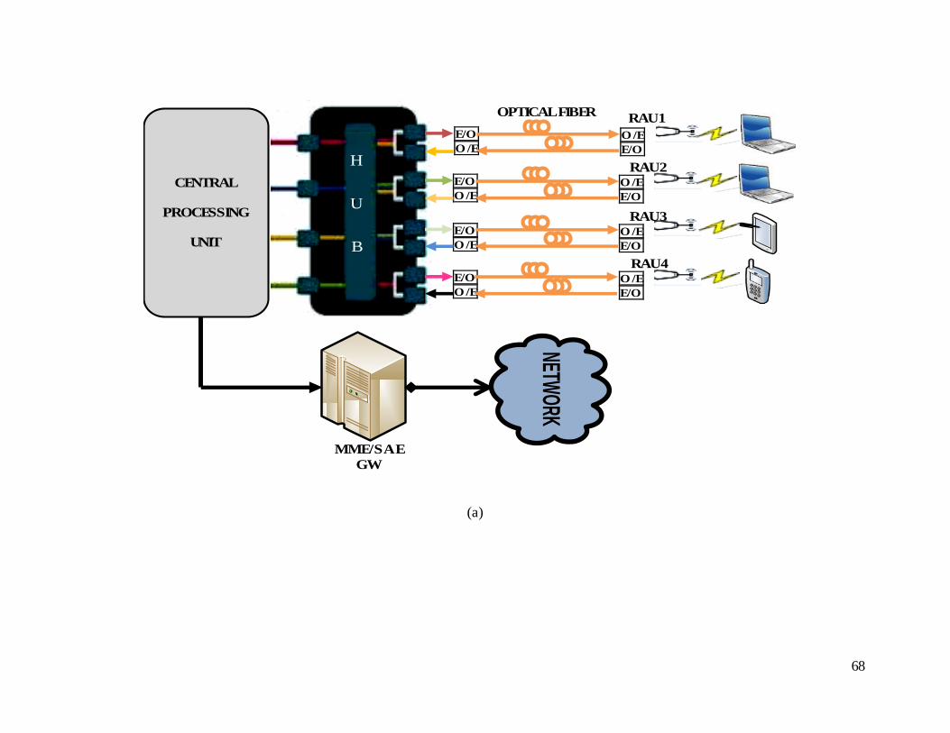
68
(a)
CENTRAL
PROCESSING
UNIT
E/O
O /E
E/O
O /E
E/O
O /E
E/O
O /E
O /E
E/O
O /E
E/O
O /E
E/O
O /E
E/O
H
U
B
RAU 1
RAU 2
RAU 3
RAU 4
OPTICAL FIBER
NETWORK
MME/SAE
GW

69
(b)
(c)
Figure 3.7: Deployment diagram of 4G LTE-A ROF systems having centralized
architecture. (a) Overview of centralized eNB architechture . (b)
Transmitter unit. (c) Receiver unit.

70
convertor & amplifier and a RF antenna at 2.4/5 GHz band to transmit or receive radio
signals. The RAU‟s are relatively close to the user equipment generally within few hundred
meters. So, an ITU pedestrian multipath channel with Doppler frequency fd = 5Hz is chosen
for simulations.
Fig. 3.7(b) and (c) shows the transmitter and receiver unit of the proposed
architecture. In the first step of the transmitter processing, the user data is generated
depending on the previous Acknowledgement (ACK) signal. If the previous user data
Transport Block (TB) was not acknowledged, the stored TB is retransmitted using a Hybrid
Automatic Repeat reQuest (HARQ) scheme. The data of each user is independently encoded
using a turbo encoder [12]. The encoding process is followed by the data modulation, which
maps the channel-encoded TB to complex modulation symbols. Depending on the CQI, a
modulation scheme is selected for the corresponding Resource block. Modulation schemes
used for downlink-shared channel (DL-SCH) here are QPSK, 16-QAM, and 64-QAM. The
modulated transmit symbols are then mapped to a MIMO precoding matrix. The optimum
precoding matrix is selected from a code book depending on the Pre-coding Control
Information (PCI) that is fed back from the UE to the transmitter. Finally, the individual
symbols to be transmitted are mapped to the resource elements. Downlink reference symbols
and synchronization symbols are also inserted into the OFDM/OWDM time-frequency grid.
The assignment of a set of resource blocks (RBs) to UEs is carried out by the scheduler based
on the CQI reports from the UEs.
The receiver structure is shown in Fig. 3.7(c). Each UE receives the signal transmitted
by the eNB and per-forms the reverse physical-layer processing of the transmitter. First, the
receiver has to identify the RBs that carry its designated information. The estimation of the

71
channel is performed using the reference signals available in the resource grid. The channel
knowledge is also used for the demodulation and soft-decoding of the OFDM/OWDM signal.
In case of MIMO, a MMSE decoder is used. Finally, the UE performs HARQ combining and
channel decoding. In order to cut down processing time after end of every turbo iteration a
CRC check of the decoded block is performed and if correct, decoding is stopped.
Standard QoS parameters BER and throughput have been compared for OFDM and
OWDM architectures using the above system model. In addition, a performance evaluation
of radio over single mode fiber system using coded OFDM and OWDM and the relation of
fiber length with BER is discussed. Moreover, PAPR is a well-known demerit in OFDM
based systems. So, a comparison is also drawn between PAPR in the two systems.
3.6.1 Bit-Error-Rate Comparison
Figs. 3.8(a), 3.8(b) and 3.8(c) shows the simulation results for bit-error-rate versus
signal to noise ratio for OWDMA/OFDMA systems at different modulation formats. Table
3.6 shows the parameters used for the simulations. The plots are drawn for modulation
Table 3.6: Simulation parameters
PARAMETER VALUE
CHANNEL BANDWIDTH 20 MHZ
MODULATION SCHEMES QPSK, 16-QAM, 64-QAM
MULTIPLE ACCESS
ARCHITECTURES OWDMA/OFDMA

72
PARAMETER VALUE
N (SIZE OF COMPUTATION) 1024
ERROR CONTROL CODE RATE-1/2 TURBO CODES
CHANNEL MODEL ITU EXTENDED PEDESTRIAN A MODEL (EPA) WITH
Fd= 5HZ
schemes of QPSK, 16-QAM and 64-QAM for an ITU defined EPA with Doppler frequency
fd= 5Hz. The size of transform for both the architectures is taken as 1024 for a total of 50
resource blocks at 20MHz bandwidth. Comparisons are drawn taking both uncoded and rate-
1/2 turbo coded OWDMA/OFDMA systems. We can infer from the graphs that OWDMA
perfoms better than OFDMA for both coded and uncoded schemes. At QPSK modulation as
in Fig. 3.8(a), OWDMA shows a performance improvement close to 1.5dB which increases
to nearly 2.5dB for 64-QAM modulation as shown in Fig. 3.8(c). The gain in SNR can be
used to either increase reach or accommodate more number of users.
The relation of optical fiber length in terms of performance (SNR of radio-over-fiber)
with BER is shown in Fig. 3.8(d). Table VII defines the simulation parameters for the
optical link. The SNR of radio-over-fiber is defined as the ratio of probe power (PFIBER) of
the fiber and the total noise in the ROF system. Total noise of the ROF system is the sum of
Additive White Gaussian Noise (AWGN) plus the fiber nonlinearities and it passes through
an ITU multipath fading channel (EPA channel) as defined in the previous case. The SNR of
ROF is given by Eqn. (3.20), where, h is the radio channel coefficient and NAWGN & NFIBER-
NL are the AWGN noise & degradation from fiber nonlinearities respectively.
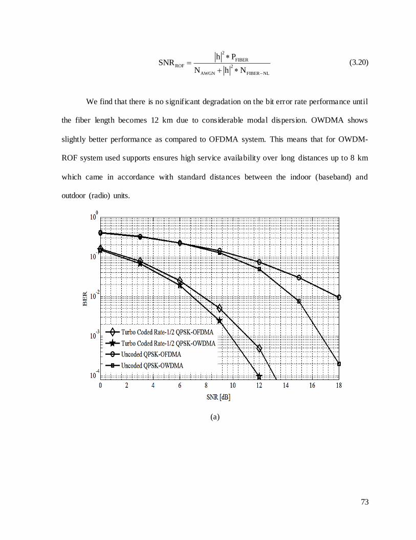
73
2
FIBER
ROF 2
AWGN FIBER NL
h PSNR
N h N
(3.20)
We find that there is no significant degradation on the bit error rate performance until
the fiber length becomes 12 km due to considerable modal dispersion. OWDMA shows
slightly better performance as compared to OFDMA system. This means that for OWDM-
ROF system used supports ensures high service availability over long distances up to 8 km
which came in accordance with standard distances between the indoor (baseband) and
outdoor (radio) units.
(a)

74
(b)
(c)

75
(d)
Figure 3.8: Signal to noise ratio versus bit error rate comparison for OWDMA and
OFDMA architectures in LTE A ROF systems. (a) Signal to noise ratio
versus bit error rate comparison for rate-1/2 turbo-coded & uncoded
QPSK-OWDMA and QPSK-OFDMA. (b) Signal to noise ratio versus bit
error rate comparison for rate-1/2 turbo-coded & uncoded 16QAM-
OWDMA and 16QAM-OFDMA. (c) Signal to noise ratio versus bit error
rate comparison for rate-1/2 turbo-coded & uncoded 64QAM-OWDMA
and 64QAM-OFDMA. (d) Signal to noise ratio (radio-over-fiber) versus
bit error rate comparison for QPSK-OWDMA and QPSK-OFDMA at
different fiber lengths.

76
Table 3.7: Fiber parameters in optical link
Parameter Value
Type of Fiber Single Mode Non-Zero Dispersion Shifted Fiber
(NZDSF)
Fiber Wavelength 1.55 μm
Fiber Dispersion 4 ps/nm-km
Fiber attenuation 0.21 dB/km
Frequency Spacing 50 GHz
Optical Probe Power 15 dBm
Span Length 1 km, 8 km & 12 km
3.6.2 Throughput Of OWDMA System
In this section we compare the throughput results of OWDMA systems as compared
to OFDMA systems. In a fading system, the capacity of a MIMO system is given by [3]
2C B F log 1 M SNR
(3.21)
Here, SNR is the Signal to Noise Ratio, B the bandwidth occupied by the data
subcarriers, β defines combined path-loss and lognormal shadowing at any RAU, M is the
number of RAU‟s and F is a correction factor. The transmission of an OFDM signal requires
also the transmission of a CP to avoid inter-symbol interference and the reference symbols

77
for channel estimation. The correction factor F represents the loss due to cyclic prefix. In
order to avoid any Inter Symbol Interference (ISI), the symbol time should be greater than
the channel delay spread. The substreams should also be orthogonal to each other and thus
OFDM is used. Assume the transmission of a sequence, x[n] = {x[0],x[1], . . . ,x[N - 1]},
with the size of N, through a channel with L multipaths, h[l] = {h[0], h[1], . . . , h[L -1]}. We
assume that the channel consists of L distinct and resolvable paths and v[n] is assumed to be
AWGN. So, the discrete sampled received signal, r[n], at the output of the channel can be
written as
L 1
l 0
r n h l x n v n
(3.22)
It is well known that multiplication in the DFT domain corresponds to the circular
convolution in the time domain. In order to achieve circular convolution using linear
convolution, we must add a prefix that is the „cyclic prefix‟ onto the transmitted signal. This
cyclic prefix makes the linear convolution appear as a circular convolution, and represents a
loss in the achievable data rate that becomes significant in the highly fading channels. But in
the case of OWDM that uses wavelet transform, the operations involves shift and multiply
operations with filter coefficients. The shift by two for subsequent pairs of rows produces a
downsampling operation within the matrix transformation and also makes the matrix
orthogonal and circulant [59]. Therefore, a cyclic prefix is not required in the case of OWDM.
This gives a significant throughput advantage particularly in highly dispersive channels. The
proof of this is given in Appendix B.

78
Figure 3.9: Signal to noise ratio versus throughput (spectral efficiency) for OWDMA
and OFDMA systems at different values of M
Fig. 3.9 shows the throughput [Mb/s] versus SNR in dB with values of M (RAU‟s)
ranging from 1-4 for OWDM and OFDM systems. Shannon‟s limit for the capacity at
different M is also drawn to show the upper bound. The red circles depict the throughput for
OWDM/OFDM at a particular modulation scheme and SNR. It is found that for the OWDM
system achieves better throughput at same channel conditions putting less burden on the
overall resources in terms of modulation used at a given SNR. For instance, OWDM with
QPSK provides 25% better throughput performance as compared to OFDM with 16-QAM
between 12-14 dB SNR. Data Rate upto 760 Mb/s can be achieved using OWDM systems
and the results are very close to Shannon‟s limit. Thus, OWDM is not only a more efficient
system than OFDM but an optimum system that performs close to Shannon‟s limit.

79
3.6.3 Peak Average To Power Ratio
PAPR appears to be a main disadvantage of OFDM. In this chapter we show that
PAPR performance in OWDMA is better than that of the OFDMA systems. PAPR depends
on the bandwidth efficiency of the system. The problem of high PAPR is usually associated
with OFDM because it is much easier to reach high bandwidth efficiency for OFDM. There
exist a large number of publications in literature devoted to the PAPR problem in OFDM.
But these publications almost claim only a slight improvement on the exiting architecture.
But, the results of tests indicate OWDM is the ideal candidate to solve the existing PAPR
issues and still deliver high bandwidth efficiency. Our PAPR simulation and analysis is
carried out based on its complementary cumulative distribution (CCD). So, for a given
PAPR0 (dB), the percentage of combinations that guarantee (PAPR > PAPR0) is a
meaningful criterion for analysis purposes. In general, the PAPR of wavelet coefficients
coming out is defined in Eqn. (3.23) as the ratio between the maximum instantaneous power
and its average power, where E[Wc(t)]2 is the average power of Wc(t) (Wavelet Coefficients).
2
C
10 2
C
max W tPAPR dB 10 log
E W t
(3.23)
The PAPR performance metric we consider is the complementary cumulative
distribution function (CCDF) which is plotted as in Fig. 3.10. The OWDMA system provides
reduced PAPR of around 2 dB which is favorable for RF amplifier operation as compared to
OFDMA systems.

80
Figure 3.10: CCDF plot of PAPR in dB
3.6.4 Inter Carrier Interference
The main disadvantage of OFDM, however, is its susceptibility to small differences
in frequency at the transmitter and receiver, normally referred to as frequency offset as
shown in Fig. 3.11. This frequency offset can be caused by Doppler shift due to relative
motion between the transmitter and receiver, or by differences between the frequencies of the
local oscillators at the transmitter and receiver. In this section, the frequency offset is
modeled as a multiplicative factor introduced in the channel, as shown in Figure
Figure 3.11: Frequency offset model
81
The received signal is given by,
j2 n
Ny n x n e w n
(3.24)
Where ε the normalized frequency offset, and is given by ∆fNTs, ∆f is the frequency
difference between the transmitted and received carrier frequencies and Ts is the subcarrier
symbol period. w(n) is the AWGN introduced in the channel.
The effect of this frequency offset on the received symbol stream can be understood by
considering the received symbol Y(k) on the kth sub-carrier is
N 1
k
l 0,l k
Y k X k S 0 X l S l k n
k 0,1,2,.........N 1
(3.25)
Where N is the total number of subcarriers, is the transmitted symbol (M-ary phase-shift
keying, for example) for the kth subcarrier, nk is the FFT of and are the complex coefficients for
the ICI components in the received signal. The ICI components are the interfering signals
transmitted on sub-carriers other than the kth sub-carrier. ICI power is calculated by Eqn. (3.26)
where h is the impulse response, n is the up-sampling factor of data X and with M-ary
modulation [60]
M 1
22
ICI jkp k
k 0,k j m
h n m
(3.26)

82
Figure 3.12: ICI power of OWDM & OFDM systems
Fig. 3.12 shows the Inter Carrier Interference power generated with the increasing
number of subcarriers in OWDM and OFDM systems. The interference power for OWDM
system shows an exponential decrease whereas in the OFDM system it decreases linearly.
3.7 Summary
In this chapter, we have developed a flexible, hardware friendly and low-power
OWDMA architecture design for deployment in ROF systems having LTE-A configuration.
The key contribution of the paper is the architecture derived for a LTE A-ROF system with
an interface of input and output ports that can replace the OFDMA block with ease giving
added benefits.
We first derived the architecture based on previous 9/7 lifting scheme wavelet filters.
The computation of the method is described using filters, controller and parallel-to-serial
units. The scheduler is also implemented for easy interfacing of the sub-block with other
blocks of the system. The architecture is validated on a centralized processor having Xilinx

83
virtex-6 FPGA‟s at N=512. We compare our architecture with various other 1-D 9/7 wavelets
available in literature as well with existing OFDMA implementations. We also compute the
communication Quality parameters BER, throughput and PAPR for OWDMA and compare
with existing OFDMA systems.
We found that our architecture runs at a speed of 142.13 MHz consuming only 143
mW of power. It is better in terms of resource consumption as compared to other similar 1-D
9/7 implementations. We also found to be significantly better than OFDMA systems in terms
of resource utilization and BER, throughput and PAPR performance for ROF systems. Hence,
it was shown that OWDMA systems are well suited for high data rate applications and also
can accommodate more number of users.

84
Chapter 4
Fast Inverse Square Root Based
Matrix Inverse For MIMO-LTE
Systems
Most of the channel estimation process needs to invert a matrix which is either the
channel state information or a nonlinear function of it. If increasing the number of
transmitter and receiver antennas is to provide a higher data rate as described in section 2.7.4
Enhanced MIMO proposal in LTE-A. Consequently the dimension of matrix function
increases and it requires more computations to invert the matrix in fewer times. Thus we
require fast approaches to obtain matrix inverse. In this chapter, we will be presenting a
floating point based matrix inversion technique using FISRMI based givens rotation and will
optimize it for speed and power. We propose an approach explained in sections below that
replaces the square root and division operation in matrix inverse by shift and multiply
operations. Thus it reduces latency and increases speed as compared to other architectures.

85
4.1 Matrix Inversion Using QR Decomposition And
Systolic Array
The complexity of matrix inversion in hardware becomes prohibitive for real time
applications and large values of n. In this report we present the results for inverting a matrix
of size 4× 4. The same idea and a slight modification in hardware can be used for larger
matrix sizes. In the hardware design, we are using QR decomposition and systolic arrays [61].
A QR
(4.1)
Let A be n× p matrix of full rank p. The QR decomposition is decomposing matrix A
to a triangular matrix Rp× p and an orthogonal matrix Q using plane rotations.
1 1
1 H H H H 1 HA A A A R R R Q R Q
(4.2)
Here, H is the hermition transpose of a matrix. Using systolic arrays by solving for
the equation below which has an upper triangular matrix R, we can find inverse of matrix A.
1
H 1 H
1 H
AA I
Q QRA Q I
RA Q
(4.3)
4.1.1 QR Decomposition Using Givens Rotation
Let A be n× p matrix of full rank p. An orthogonal matrix triangularization (QR
Decomposition) consists of determining an n n orthogonal matrix Q with the p p upper

86
triangular matrix R. One only has then to solve the triangular system Rx=Py ,
where P consists of the first p rows of Q .
1 0 0 0
0 c s 0
0 s c 0
0 0 0 1
(4.4)
With properly chosen c=cos ( ) and s=sin ( ) for some rotation angle can be
used to zero the element Aki (where k is the row and i is the column of A) to find a upper
triangular matrix R. The elements can be zeroed column by column from the bottom up. Q is
then the product of g=2 2n−p−1 Givens matrices Q=G1G2 Gg . The orthogona l
matrix QH is formed from the concatenation of all the Givens matrices Q
H =GgGg-1 G1.
Thus, we have R=QH A=GgGg-1 G1 A=R, and the QR decomposition is A=QR. To
annihilate the bottom element of a 2 1 vector:
T
2 2 2 2
c s a r
s c b 0
a bc ,s
a b a b
(4.5)

87
4.1.2 Fast Inverse Square Root
The operations in the givens rotation involve division and square roots which can be
quite costly to be implemented in the hardware in terms of latency and hardware. Thus,
instead of that we will use a fast inverse square root method that has only shift and addition
operations. Since for our application of MIMO-OFDM systems, 32-bit is enough for
representation. We will limit our approach for fast inverse square root to a floating point of
32-bits. Floating point numbers are stored in 2‟s complement signed format in hardware as;
Figure 4.1: 2‟s Complement signed form of floating point numbers with exponent
and mantissa
Where s is a 1 bit sign (1 denotes negative), E is an 8 bit exponent, and M is a 23 bit
mantissa. The exponent is biased by 127 to accommodate positive and negative exponents,
and the mantissa does not store the leading 1, so think of M as a binary number with the
decimal point to the left, thus M is a value in I = [0, 1). The represented value is
s Ex 1 1 M 2
(4.6)
These bits can be viewed as the f loating point representation of a real number, or
thinking only of bits, as an integer. Thus M will be considered a real number in I or as an
integer, depending on context. M as a real number is M as an integer divided by 223.
Let the
exponent E1 = E − 127. Then x = (1 + M )2E1
, and the desired value ,

88
E11 1y 2
x 1 M
(4.7)
For the general case we take a magic constant R, and analyze y0 = R−(i>>1), where
the subtraction is as integers, i is the bit representation of x, but we view y0 as a real number.
R is the integer representing a floating point value with bits
0 R1 R2
(4.8)
i.e., R1 in the exponent field and R2 in the mantissa field. When we shift i right one bit,
we may shift an exponent bit into the mantissa field, so we will analyze two cases.
1. Exponent E Even
In this case, when we use i>>1, no bits from the exponent E are shifted into the mantissa M,
and [E/2] = E/2. The true exponent e = E −127 is odd, say e = 2d + 1, d an integer. The bits
representing the initial guess give the new exponent. We require this to be positive. If it were
negative the resulting sign bit would be 1, and the method fails to return a positive number. If
this result is 0, then the mantissa part could not borrow from the exponent. The initial guess
for inverse square root is then,
1R 64 d 127
0 2y 1 R M / 2 2
(4.9)
2. Exponent E Odd
With the previous case under our belt, we analyze the harder case. The difference is that the
odd bit from the exponent E shifts into the high bit of the mantissa from the code i>>1. This
adds 12 to the real value of the shifted mantissa, which becomes [M/2] + 12 , where the
truncation is as integers and the addition is as real numbers. e = E − 127 = 2d is even. Similar
89
to above the new exponent is this must be positive as in the previous case. Now the initial
guess is,
1R 63 d 127
0 2y 1 R M / 2 1/ 2 2
(4.10)
To get a near accurate result Newton‟s method of approximation is used [62], and the
magic constant is used to compute a good initial guess. Given a fixed point value x > 0, we
want to reduce the following cost function for optimized results,
2
1f y x
y
(4.11)
Then the value we seek is the positive root of f(x). Newton‟s root finding method,
given a suitable approximation yn to the root, gives a better one yn+1 using,
n
n 1 n
n
f yy y
f y
(4.12)
For the f(y) given, this simplifies to yn+1 = 1/2 * yn(3 − xyn2), Where x is the initial
guess.
4.1.3 Systolic Architecture
Use of systolic arrays for matrix triangularization is a well known concept [36].
Systolic array is a computing communication processing which has some advantage like as
synchrony, modularity and regularity, spatial and temporal locality, pipelining etc. For

90
computation, it is simple and regular design, network and balancing computation with
input and output.
Using Eqn. 4.3, we find that RA-1
=QH. We use two computing cells, The Boundary
cells and the vectoring cells. Boundary cells move left to right in this architecture, it passes
different values to the vectoring cell from R matrix. Vectoring cells has two computation
nodes, one does division for diagonal elements of R with corresponding Q hermition matrix
and the other is a multiply and accumulate node which multiplies the values in R and
accumulates the added value. It finally subtracts and feeds the output to division node, which
finally outputs the value. This cell moves from top to bottom in the architecture. This outputs
the values in a back substitution manner.
The Fig. 4.2 below shows the block diagram for implementation in hardware. The
process is a sequential process that reuses the available resources in the system. The fast
inverse square root block is used once in every iteration, to give the output G that utilizes c
and s computed simultaneously. G is used to calculate Q hermition and R matrix finally after
6 iterations. Each of c and s uses one multiplication block. G and Q computation requires a
multiply and accumulate DSP 48 macro which can be used sequentially to optimize the
resources.

91
Figure 4.2: Block diagram of hardware model
After values of R and Q are calculated, elements of A-1
matrix are found using back
substitution of the systolic array architecture in Fig. 4.3 as per Eqn. (4.13). The div block
uses the fast inverse square root and a multiplier to do fast division. Boundary cell feeds the
R values to vectoring cell which multiplies and accumulates the data followed by division to
give the output back. All 4 values of inverse matrix of A are calculated in one block cycle.
The final output is obtained in 4 block cycles. Here, i goes from 3…1 and L, j from 1…4.

92
Figure 4.3: Systolic array architecture
ij
R11 R12 R13 R14 a11 a12 a13 a14 Q11 Q21 Q31 Q41
0 R22 R23 R24 a21 a22 a23 a24 Q12 Q22 Q32 Q42
0 0 R33 R34 a31 a32 a33 a34 Q13 Q23 Q33 Q43
0 0 0 R44 a41 a42 a43 a44 Q14 Q24 Q34 Q44
a
N 4
ij iL Lj
L i 1
ii
Q R a
R
(4.13)
4.2 FPGA Implementation And Analysis
The System Generator, a high level design tool from Xilinx is used to implement and
test the matrix inversion design on the Virtex6-xc6vsx475t FPGA. Input is a 4 × 4 matrix of
32-bit floating point value and output is the inverse matrix. Table 4.1 shows the design
statistics for a 4 × 4 matrix inversion core using our method with that of other methods like
CORDIC based SGR and SDGR. Compared to other methods, we save a lot in computation

93
time due to elimination of division & square roots with a slight increase in no. of additions
and multiplications. We assumed 8 bits for mantissa, 23 bits for exponent of floating point
numbers and one sign bit. For floating point operators (adder and multiplier) we have used
the available operators of DSP 48 from Xilinx. All these operators are compatible with
IEEE754 standard. On a state of the art Virtex6-xc6vsx475t FPGA running at 200 MHz, this
matrix inversion architecture achieves a throughput of 0.29μs or 3.5M updates per second.
These latencies can be decreased by adding more boundary or internal nodes to the design or
decreasing the word length requirements. The design is easily extendable to other matrix
sizes of n × p by changing the control unit. There is a tradeoff between number of cells (and
hence area of the design) and throughput. For larger matrices, if throughput is less than
required, we can increase number of cells and use a semi-parallel approach instead of the
current folded model.
We optimize our design by pipelining the triangular section and the back substitution
part of the design for Speed and Area respectively. We do timing and power analysis using
the modelsim software and calculate delay and power required for entire operation with and
without pipelining. Table 4.2 depicts the resources, delay and power for each of the
processess compared to the SGR [36] and CORDIC [63] methods. We can find out that
pipelining approach for speed increases the throughput to 4.4M per second and also reduces
the power utilized. The trade-off is the increase in resources. Our method outperforms
CORDIC and SGR in terms of throughput, resource utilization and latency.
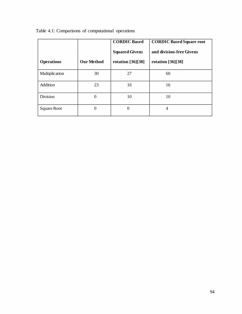
94
Table 4.1: Comparisons of computational operations
Operations Our Method
CORDIC Based
Squared Givens
rotation [36][38]
CORDIC Based Square root
and division-free Givens
rotation [36][38]
Multiplication 30 27 60
Addition 23 16 16
Division 0 10 10
Square Root 0 0 4

95
Table 4.2: Resource estimation of 4x4 matrix inversion core
OUR TECNIQUE
W/O PIPELINING
SPEED OPTIMIZED
USING PIPELINING
AREA OPTIMIZED
USING PIPELINING CORDIC [63]
SGR
[36][38]
Slices 6219 8721 8922 16865 9117
DSP 48 39 38 37 - -
RAM 9 9 4 - -
IOB 62 127 127 - -
Latency 0.29μs 0.23μs 0.25μs 45.5 μs 8.1 μs
Throughput 3.5M 4.4M 4M - 0.13M
Power 4.8W 4.4W 4.4W - -

96
4.3 LTE MIMO MMSE Matrix Inversion BER
In this manuscript, to show the effect of wordlength on the accuracy of matrix
inversion and channel estimation, the 16 bit and 20 bit representations are evaluated for the
inverse of large 4x4 and 8x8 matrices using 16-QAM and 64-QAM modulation. If we
assume X(k) & R(k) as the transmitted and received sequences respectively, H(k) as the
channel coefficients and N(k) as the additive white Gaussian noise of variance σ, then R(k) is
given by,
R(k) H(k)X(k) N(k)
(4.14)
Here X(k) and R(k) € (M-QAM symbols) and are NR x 1 row vector. NR is the number
of receive antenna € (4 or 8 in our case = NT transmit antennas). H(k) is NR x NT vector and
N(k) € σ2
INx1 vector. The Xest (k) is the estimated value of X(k) given by MMSE decoder as,
1
H 2 H
est NX k H k H k I H k R k
(4.15)
Fig. 4.4 (a) & (b) shows the comparison of BER versus SNR curves of MMSE
decoders using the FISRMI and CORDIC 16-bit and 20-bit. Although the 16-bit and 20-bit
provides enough precision for inversion of small matrices, the error increases substantially at
higher SNRs. CORDIC saturates with increase in SNR. Hence the floating point FISRMI
approach would be much better suited for use in future LTE systems using larger matrices.
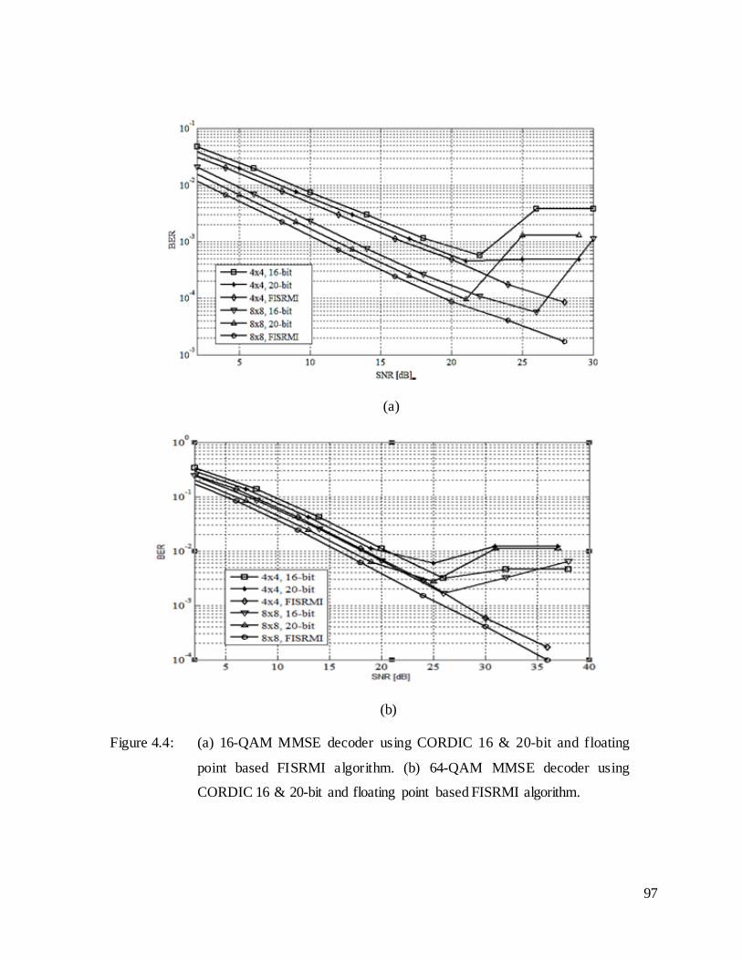
97
(a)
(b)
Figure 4.4: (a) 16-QAM MMSE decoder using CORDIC 16 & 20-bit and floating
point based FISRMI algorithm. (b) 64-QAM MMSE decoder using
CORDIC 16 & 20-bit and floating point based FISRMI algorithm.

98
4.4 Summary
A matrix inversion core is designed and implemented on Xilinx Virtex6 FPGAs using
fast inverse square root based QRD and Givens Rotation algorithms. The design runs with a
clock rate of 200 MHz and achieves a throughput of 4.4M updates per second with
optimization using pipelining. This design is easily extendable to other matrix sizes. We also
compare BER versus SNR of FISRMI algorithm with CORDIC 16-bit and 20-bit method and
demonstrated our method to be better for inversion of higher matrices.

99
Chapter 5
Conclusion
5.1 Summary Of Contributions
In this thesis, we have formulated, derived and evaluated OWDMA Architecture
(Chapter 3). We started with basic wavelet transform and developed the methodology and
optimized hardware structure. The architecture was evaluated for resources, efficiency,
Throughput and bit error rate performance against the state of the art OFDMA multiple
access scheme (Chapter 2). It gives superior performance in all the metrics. Apart from that it
consumes less power, mitigates PAPR and ICI problem significantly compared to OFDMA.
We think it is a novel concept since no such multiple access for wireless communication
system exists in the literature and neither its hardware architecture been developed and
synthesized & evaluated thoroughly.
In Chapter 4, we have developed a new FISRMI. The method is new in the way
because all the matrix inverse present in the literature focuses on either CORDIC rotation,
Householder matrix inverse, Gram-Schmidt based QR inverse & divide and conquer matrix
inverse. Eliminating complex calculations of square root and division has never been done
before. In addition, the floating point implementation approach gives better resolution and

100
accuracy to the receiver decoding. This saving in SNR can be used in many ways to improve
the quality of service to end users.
5.2 Future Directions
Our OWDMA architecture was shown to be better in architecture and simulation
(Chapter 3). However, the actual implementation on test bed is needed to verify our synthesis
and simulation results. We simulated BER vs SNR for different fiber length at a single
launch power and for single mode NZDSF fibers. We will need to evaluate more fibers
lengths as well as different fiber levels. Multi-mode fibers also have to be tested against the
single mode fibers at short lengths in presence of link noise.
The adaptability of our method has to be experimentally evaluated at different
channel conditions and in different changing environments like office, urban, sub-urban and
desert. Support to number of users in a busy area and in tunnels & subways have to be
substantiated at those conditions. Downlink and uplink speeds and latency have to be
measured as well. And the overall adaptability of the architecture to the rest of system has
also to be seen and tested, so as to minimize the change in the existing architecture as much
as possible. This will save on CAPEX of the overall LTE systems and on the consumer side.
Although, the floating point matrix inverse is a very promising method, but more tests
are needed to evaluate the actual resources taken by the structure and how it can be beneficial.
Trade-off is required between SNR savings and bit resolution to implement the system in
actuality on a test-bed. If the matrix inverse block would be developed on DSP processor,
then the sending and receiving data to and from the block has to be synchronized. One of the
major problems while working with floating-point arithmetic is preventing overflows. While

101
performing arithmetic calculations, a result may not fit into the reserved bits and if this case
is not handled carefully, it causes overflow and incorrect results. So, overflow prevention
have to be taken care of while dealing in floating points.
5.3 Final Remarks
Overall the two algorithms described in the thesis has demonstrated a strong promise
to solve some of the existing problems in LTE networks as well aid in the deployment of
future LTE systems. By considering the further refinements suggested in Section 5.2, we
believe the methods provided in this thesis will contribute and motivate efforts to reach the
levels of seamless and effortless integration expected and required for an even wider-scale
deployment of LTE-A networks.
102
Bibliography
[1] C. Mahapatra, A. Ramakrishnan, T. Stouraitis, and V. C. M. Leung, “A novel
implementation of sequential output based parallel processing - orthogonal wavelet division multiplexing for DAS on SDR platform,” in 2012 19th IEEE International Conference on Electronics, Circuits, and Systems (ICECS 2012), 2012, pp. 320–323.
[2] C. Mahapatra, S. Mahboob, V. C. M. Leung, and T. Stouraitis, “Fast Inverse Square Root Based Matrix Inverse for MIMO-LTE Systems,” in 2012 International
Conference on Control Engineering and Communication Technology , 2012, pp. 321–324.
[3] S. Mahboob, C. Mahapatra, and V. C. M. Leung, “Energy-Efficient Multiuser MIMO Downlink Transmissions in Massively Distributed Antenna Systems with Predefined Capacity Constraints,” in 2012 Seventh International Conference on Broadband, Wireless Computing, Communication and Applications, 2012, pp. 208–211.
[4] H. Li, J. Hajipour, A. Attar, and V. Leung, “Efficient HetNet implementation using broadband wireless access with fiber-connected massively distributed antennas architecture,” IEEE Wirel. Commun., vol. 18, no. 3, pp. 72–78, Jun. 2011.
[5] A. Attar, H. Li, and V. Leung, “Green last mile: how fiber-connected massively
distributed antenna systems can save energy,” IEEE Wirel. Commun., vol. 18, no. 5, pp. 66–74, Oct. 2011.
[6] 3GPP, “Evolved Universal Terrestrial Radio Access (E-UTRA); Requirements for support of radio resource management,” Sep. 2008.
[7] Tao Jiang and Yiyan Wu, “An Overview: Peak-to-Average Power Ratio Reduction Techniques for OFDM Signals,” IEEE Trans. Broadcast., vol. 54, no. 2, pp. 257–268, Jun. 2008.
[8] J.P. Rissen, “Mapping the Wireless Technology Migration Path : The Evolution to 4G Systems,” Alcatel-lucent, enriching communications, vol.2, no. 1, 2008.
[9] I. T. U, “World Telecommunication Development Report 2002,” Reinventing Telecoms, Executive summary, March 2002.

103
[10] Y. Kim, B.-J. Jeong, J. Chung, C.-S. Hwang, J. S. Ryu, K.-H. Kim, and Y.-K. Kim, “Beyond 3G: vision, requirements, and enabling technologies,” Communications Magazine, IEEE, vol. 41, no. 3. pp. 120–124, 2003.
[11] S. Ohmori, Y. Yamao, and N. Nakajima, “The future generations of mobile communications based on broadband access technologies,” IEEE Commun. Mag., vol. 38, no. 12, pp. 134–142, 2000.
[12] 3GPP, “3GPP System Architecture Evolution (SAE); Security architecture.” Aug. 2008.
[13] 3GPP, “Feasibility study for evolved Universal Terrestrial Radio Access (UTRA) and Universal Terrestrial Radio Access Network (UTRAN),” Aug. 2007.
[14] 3GPP, “Evolved Universal Terrestrial Radio Access (E-UTRA); Long Term Evolution (LTE) physical layer; General description,” Dec. 2007.
[15] D. J. Love and R. W. Heath, “Limited Feedback Unitary Precoding for Spatial
Multiplexing Systems,” IEEE Trans. Inf. Theory, vol. 51, no. 8, pp. 2967–2976, Aug. 2005.
[16] J. Wannstrom, “LTE-Advanced,” 2012. [Online]. Available: http://www.3gpp.org/IMG/pdf/lte_advanced_v2.pdf.
[17] R. Irmer, H. Droste, P. Marsch, M. Grieger, G. Fettweis, S. Brueck, H.-P. Mayer, L. Thiele, and V. Jungnickel, “Coordinated multipoint: Concepts, performance, and field trial results,” IEEE Commun. Mag., vol. 49, no. 2, pp. 102–111, Feb. 2011.
[18] “Achieving Cost-Effective Broadband Coverage with WiMAX Micro , Pico and Femto Base Stations.” Fujitsu white paper, Oct. 2008.
[19] G. Horn, “3GPP Femtocells : Architecture and Protocols.” Qualcomm media documents, Sep. 2010.
[20] T. Niiho, M. Nakaso, K. Masuda, H. Sasai, K. Utsumi, and M. Fuse, “Transmission performance of multichannel wireless LAN system based on radio-over-fiber techniques,” IEEE Trans. Microw. Theory Tech., vol. 54, no. 2, pp. 980–989, Feb. 2006.
[21] G. Brown, “What Price a 3G Base Station?,” 2010. [Online]. Available: http://www.lightreading.com/document.asp?doc_id=602020.
[22] M. Sauer, A. Kobyakov, and J. George, “Radio Over Fiber for P icocellular Network Architectures,” J. Light. Technol., vol. 25, no. 11, pp. 3301–3320, Nov. 2007.

104
[23] A. Akansu, P. Duhamel, X. Lin, and M. de Courville , “Orthogonal transmultiplexers in communication: a review,” IEEE Trans. Signal Process., vol. 46, no. 4, pp. 979–995, Apr. 1998.
[24] M. K. Lakshmanan and H. Nikookar, “A Review of Wavelets for Digital Wireless Communication,” Wirel. Pers. Commun., vol. 37, no. 3–4, pp. 387–420, May 2006.
[25] C. J. Mtika and R. Nunna, “A wavelet-based multicarrier modulation scheme,” in Proceedings of 40th Midwest Symposium on Circuits and Systems. Dedicated to the Memory of Professor Mac Van Valkenburg, 1997, vol. 2, pp. 869–872.
[26] G. W. Wornell, “Emerging applications of multirate signal processing and wavelets in digital communications,” Proc. IEEE, vol. 84, no. 4, pp. 586–603, Apr. 1996.
[27] N. Erdol, F. Bao, and Z. Chen, “Wavelet modulation: a prototype for digital communication systems,” in Proceedings of Southcon ’95, 1995, pp. 168–171.
[28] S. Linfoot, M. Ibrahim, and M. Al-akaidi, “Orthogonal Wavelet Division Multiplex:
An Alternative to OFDM,” IEEE Trans. Consum. Electron., vol. 53, no. 2, pp. 278–284, 2007.
[29] A. Shadmand, R. Dilmaghani, M. Ghavami, and M. Shikh-Bahaei, “Wavelet-based downlink scheduling and resource allocation for long-term evolution cellular systems,” IET Commun., vol. 5, no. 14, pp. 2091–2095, Sep. 2011.
[30] O. Daoud, “Performance improvement of wavelet packet transform over fast Fourier transform in multiple-input multiple-output orthogonal frequency division multiplexing systems,” IET Commun., vol. 6, no. 7, p. 765, 2012.
[31] A. Jamin and P. Mähönen, “Wavelet packet modulation for wireless communications : Research Articles,” Wirel. Commun. Mob. Comput., vol. 5, no. 2, pp. 123–137, Mar. 2005.
[32] M. Mathew, A. B. Premkumar, and C. T. Lau, “Multiple Access Scheme for Mult i
User Cognitive Radio Based on Wavelet Transforms,” in 2010 IEEE 71st Vehicular Technology Conference, 2010, pp. 1–5.
[33] G. Lightbody, R. Walke, R. Woods, and J. McCanny, “Linear QR Architecture for a Single Chip Adaptive Beamformer,” J. VLSI signal Process. Syst. signal, image video Technol., vol. 24, no. 1, pp. 67–81, Feb. 2000.
[34] C. Singh, S. Prasad, and P. Balsara, “VLSI Architecture for Matrix Inversion using Modified Gram-Schmidt based QR Decomposition,” in 20th International Conference on VLSI Design held jointly with 6th International Conference on Embedded Systems (VLSID’07), 2007, pp. 836–841.

105
[35] A. Maltsev, V. Pestretsov, R. Maslennikov, and A. Khoryaev, “Triangular systolic array with reduced latency for QR-decomposition of complex matrices,” in 2006 IEEE International Symposium on Circuits and Systems, 2006, p. 4.
[36] M. Karkooti, J. R. Cavallaro, and C. Dick, “FPGA Implementation of Matrix Inversion Using QRD-RLS Algorithm,” in Conference Record of the Thirty-Ninth Asilomar Conference onSignals, Systems and Computers, 2005. , 2005, pp. 1625–1629.
[37] B. Cerato, G. Masera, and P. Nilsson, “Hardware architecture for matrix factorization
in mimo receivers,” in Proceedings of the 17th great lakes symposium on Great lakes symposium on VLSI - GLSVLSI ’07, 2007, p. 196.
[38] J. Götze and U. Schwiegelshohn, “A Square Root and Division Free Givens Rotation for Solving Least Squares Problems on Systolic Arrays,” SIAM J. Sci. Stat. Comput., vol. 12, no. 4, pp. 800–807, Jul. 1991.
[39] S. L. Linfoot, “Wavelet families for orthogonal wavelet division multiplex,” Electron. Lett., vol. 44, no. 18, p. 1101, 2008.
[40] N. R. Raajan, B. Monisha, M. Ram Kumar, A. Jenifer Philomina, M. V. Priya, D. Parthiban, and S. Suganya, “Design and implementation of orthogonal wavelet division multiplexing (OHWDM) with minimum bit error rate,” in 3rd International
Conference on Trendz in Information Sciences & Computing (TISC2011), 2011, pp. 122–127.
[41] T. Xu, G. Leus, and U. Mitra, “Orthogonal wavelet division multiplexing for wideband time-varying channels,” in 2011 IEEE International Conference on Acoustics, Speech and Signal Processing (ICASSP), 2011, pp. 3556–3559.
[42] B. A. Liew, S. M. Berber, and G. S. Sandhu, “Performance of a Multiple Access Orthogonal Wavelet Division Multiplexing System,” in Third International Conference on Information Technology and Applications (ICITA’05), 2005, vol. 2, pp. 350–353.
[43] H. Liao, M. K. Mandal, and B. F. Cockburn, “Efficient Architectures for 1-D and 2-D
Lifting-Based Wavelet Transforms,” IEEE Trans. Signal Process., vol. 52, no. 5, pp. 1315–1326, May 2004.
[44] P. McCanny, S. Masud, and J. McCanny, “Design a nd implementation of the symmetrically extended 2-D Wavelet Transform,” in IEEE International Conference on Acoustics Speech and Signal Processing, 2002, vol. 3, pp. III–3108–III–3111.
[45] S. Raghunath and S. Aziz, “High Speed Area Efficient Multi-resolution 2-D 9/7 filter DWT Processor,” in 2006 IFIP International Conference on Very Large Scale Integration, 2006, pp. 210–215.

106
[46] S. Masud and J. V. McCanny, “Reusable Silicon IP Cores for Discrete Wavelet Transform Applications,” IEEE Trans. Circuits Syst. I Regul. Pap., vol. 51, no. 6, pp. 1114–1124, Jun. 2004.
[47] I. S. Uzun and A. Amira, “Framework for FPGA-based discrete biorthogonal wavelet transforms implementation,” IEE Proc. - Vision, Image, Signal Process., vol. 153, no. 6, p. 721, 2006.
[48] Y. T. Chan, Wavelet Basics. Springer, 1994, p. 134.
[49] I. Daubechies, Ten Lectures on Wavelets (CBMS-NSF Regional Conference Series in Applied Mathematics). SIAM: Society for Industrial and Applied Mathematics, 1992, p. 377.
[50] S. G. Mallat, “A theory for multiresolution signal decomposition: the wavelet
representation,” IEEE Trans. Pattern Anal. Mach. Intell., vol. 11, no. 7, pp. 674–693, Jul. 1989.
[51] S. Linfoot, “A study of different wavelets in orthogonal wavelet division multiplex for DVB-T,” IEEE Trans. Consum. Electron., vol. 54, no. 3, pp. 1042–1047, Aug. 2008.
[52] C. Cheng and K. K. Parhi, “High-Speed VLSI Implementation of 2-D Discrete Wavelet Transform,” IEEE Trans. Signal Process., vol. 56, no. 1, pp. 393–403, Jan. 2008.
[53] A. N. Akansu, M. V. Tazebay, M. J. Medley, and P. K. Das, “Wavelet and subband transforms: fundamentals and communication applications,” IEEE Commun. Mag., vol. 35, no. 12, pp. 104–115, 1997.
[54] W. Sweldens and I. Daubechies, “Factoring Wavelet Transforms into Lifting Steps.,” J. Fourier Anal. Appl. [[Elektronische Ressource]], vol. 4, no. 3, pp. 247–270, 1998.
[55] Q. Wang and S. B. K. Vrudhula, “An investigation of power delay trade-offs for dual Vt CMOS circuits,” Computer Design, 1999. (ICCD ’99) International Conference on. pp. 556–562, 1999.
[56] C. Zhang, C. Wang, and M. O. Ahmad, “A Pipeline VLSI Architecture for High-
Speed Computation of the 1-D Discrete Wavelet Transform,” IEEE Trans. Circuits Syst. I Regul. Pap., vol. 57, no. 10, pp. 2729–2740, Oct. 2010.
[57] Y.-W. Lin and C.-Y. Lee, “Design of an FFT/IFFT Processor for MIMO OFDM Systems,” IEEE Trans. Circuits Syst. I Regul. Pap., vol. 54, no. 4, pp. 807–815, Apr. 2007.

107
[58] Hang Liu and Hanho Lee, “A high performance four-parallel 128/64-point radix-24
FFT/IFFT processor for MIMO-OFDM systems,” in APCCAS 2008 - 2008 IEEE Asia Pacific Conference on Circuits and Systems, 2008, pp. 834–837.
[59] R. Dilmaghani and M. Ghavami, “Comparison between wavelet-based and Fourier-based multicarrier UWB systems,” IET Commun., vol. 2, no. 2, p. 353, 2008.
[60] B. G. Negash and H. Nikookar, “Wavelet-based multicarrier transmission over multipath wireless channels,” Electron. Lett., vol. 36, no. 21, p. 1787, 2000.
[61] M. A. L. Sarker and Moon-Ho Lee, “High speed MIMO LTE application based on matrix inversion algorithms using floating point DSP.” pp. 1–5, 2011.
[62] T. Dence, “Cubics, Chaos and Newton‟s Method,” Math. Gaz., vol. 81, no. 492, pp. 403 – 408, 1997.
[63] R. Hamill, J. V. McCanny, and R. L. Walke, “Online CORDIC algorithm and VLSI architecture for implementing QR-array processors,” IEEE Trans. Signal Process., vol. 48, no. 2, pp. 592–598, 2000.
[64] C. Shuang-yan, W. Dong-hui, Z. Tie-jun, and H. Chao-huan, “Design and
Implementation of a 64/32-bit Floating-point Division, Reciprocal, Square root, and Inverse Square root Unit,” in 2006 8th International Conference on Solid-State and Integrated Circuit Technology Proceedings, 2006, pp. 1976–1979.
[65] E. Hossain, V.K. Bhargava, and G. P. Fettweis (Eds.), "Green Radio Communication Networks," Cambridge University Press, August 27, 2012.

108
Appendix A
Experimental Test Bed Setup
The experimental test bed setup described here includes one central processor with
multiple distributed antenna nodes and multiple mobile stations. This setup simulates in real
time. The test bed will operate in the 2.4 GHz ISM band for its license-exempt convenience.
To achieve full flexibility to the design of the physical layer functions, MAC protocols and
Radio Resource Management (RRM) algorithms, we will employ high-speed SDR platforms
based on digital signal processors and FPGAs to realize the central access point and mobile
stations. Each platform consists of RF front-ends with 20 MHz to 80 MHz bandwidth, a
number of 125 MHz~250 MHz 14bit ADCs/DACs mounted on latest Xilinx Virtex-6 FPGA
board to pre-process data samples, and a powerful DSP/FPGA processing unit that uses
Xilinx Virtex-6 FPGAs . Zinwave 3000 DAS is used as the hub to create a 2x2/4x4 system.
Single mode NZDSF optical fibers are used to connect the DAS to the Remote radio heads.
Test Bed Architecture
In order to reduce CAPEX the test bed is developed using generic “off-the-shelf”
platforms like Micro-TCA and Advanced Mezzanine Card (AMC). On the other hand, legacy
proprietary platforms have been used until 3G/3.5G network era. Micro-TCA platform is one
of the powerful options dedicated to applying telecom equipment especially for the use in
LTE eNB. Many component venders are developing modules based on general purpose

109
Micro-TCA modules with powerful CPU, DSP, and FPGA, with high speed memory with
GbE I/F on front side. The baseband function and network interface function are
implemented on different modules. FPGAs are used for implementation of PHY/Baseband,
Digital Signal Processors or Network processors for Lower layer protocols
(HARQ/MAC/RLC), and CPUs or Network processors with operating system for upper
layers which drive the whole system. The test bed lab setup is shown in Fig. A.1 below.
Figure A.1: Test bed experimental setup
Setup Components
The three tables below specify the Test hardware requirements, Lab equipments
required and software tools needed for the test setup.

110
Table A.1: Test hardware requirements
Product Manufacturer
8xPerseus 6013 with ADAC 250 Lyrtech
4x Twin WiMAX RF Transceiver Lyrtech
5x µTCA chasis Vadatech
8x Mestor Breakout Box Lyrtech
4x JTAG FPGA Pod Xilinx
40xSMA-to-MMCX Cables Lyrtech
8xUSB to UART Cable SiLabs
8xGPIO-32 Flat Ribbon Cable Lyrtech
11xPower Adaptors Cincon Technologies
8xAntennas 2.5GHz-2.7GHz Lyrtech
8xAntennas 2.4GHz-2.48GHz Lyrtech
Distributed Antenna System Hub Zinwave
10x100 m Single Mode Fiber Corning
4xRemote Antenna Units Zinwave
Table A.2: Lab test equipment
Instrument Manufacturer Version
Vector Signal Analyzer (4GHz)(VNA master)
Anritsu MS2034A
Agilent N9030A
RF Signal Generator (4GHz) Agilent 8648D
BER Tester Agilent 8613A
Real time Oscilloscope Tektronix DRO4054

111
Instrument Manufacturer Version
Pulse Generator (1Hz-150MHz) Agilent 8110A
PSG Analog Signal Generator(250kHz-20GHz) Agilent E8257D
Table A.3: Software tools
Software Development Tools Vendor Version
MATLAB Mathworks R2009b
ISE Design Suite Xilinx 12.1
Chip Scope Pro Xilinx 12.1
iMPACT Xilinx 12.1
Sysgen Xilinx 12.1
Visual Studio Microsoft 2010
Petalinux PetaLogix SDK v2.1
µtCA Edition ADP software tools Lyrtech V5
Windows XP Microsoft SP3
112
Appendix B
Proof Of Not Requiring Cyclic Prefix
In OWDMA
From signal processing theory, it is well known that multiplication in the DFT
domain corresponds to the circular convolution in the time domain, that is
FrequencyDomain : R k H k X k
TimeDomain : r n h n x n
(B.1)
Where indicates the circular convolution, H(k) and X(k) are channel coefficients
and input respectively and R(k) is the convolved output signal. So, from Eqn. (B.1) it is
implied that in order to achieve circular convolution using linear convolution, we must add a
prefix called the „cyclic prefix‟ onto the transmitted signal. This cyclic prefix makes the
linear convolution appear as a circular convolution, and represents a loss in the achievable
data rate that becomes significant in the highly dispersive channels.
OWDM uses wavelet transform that divides the input signal into high pass (G[N])
and low pass (F(N)) components respectively. If we assume A[N] and Wc[N] as the scaling
and wavelet coefficients respectively, then we can write the scaling and wavelet coefficients
in terms of high pass and low pass components.

113
j j 1
n
A k A n F n 2k
(B.2)
j j 1
n
W k W n G n 2k
(B.3)
These two high pass and low pass coefficients are related to each other and together
form a Quadrature Mirror Filter (QMF). If U is the filter length then F[k] and G[K] are
mirror images of each other as shown in Eqn. (B.4).
k
G k 1 F U k
(B.4)
Following Eqn. (B.1) - (B.3) and computing discrete wavelet transform on received signal
r[n], we get
TM 1 M 1
n 0 n 0
TM 1 M 1 M 1 M 1
n 0 l 0 n 0 l 0
DWT(r n ) r n F n 2k r n G n 2k
h l s n l F n 2k h l s n l G n 2k
(B.5)
Taking, n-l = i, and 2k-l = m, we get
T
M 1 M 1 M 1 M 1
l 0 i 0 l 0 i 0
1 2
DWT(r n ) h l s i F i 2m h l s i G i 2m
(B.6)

114
Where Δ1 and Δ2 are (left) circular convolution between the input sequence and the
low-pass and high-pass filter coefficients, respectively. Therefore Eqn. (B.6) can be written
as in Eqn. (B.7)
T
T T
DWT k kR k DWT s n h n H F S H G S
(B.7)
Here Fk and Gk are left circulant matrices. This proves that DWT achieves circular
convolution in time domain by its inherent property and a cyclic prefix need not be added to
make it appear circular.