advanced architectures for efficient mm-wave cmos wireless
TRANSCRIPT

Advanced Architectures for Efficient mm-Wave CMOS
Wireless Transmitters
JiaShu Chen
Electrical Engineering and Computer SciencesUniversity of California at Berkeley
Technical Report No. UCB/EECS-2014-42
http://www.eecs.berkeley.edu/Pubs/TechRpts/2014/EECS-2014-42.html
May 1, 2014

Copyright © 2014, by the author(s).All rights reserved.
Permission to make digital or hard copies of all or part of this work forpersonal or classroom use is granted without fee provided that copies arenot made or distributed for profit or commercial advantage and that copiesbear this notice and the full citation on the first page. To copy otherwise, torepublish, to post on servers or to redistribute to lists, requires prior specificpermission.

Advanced Architectures for Efficient mm-Wave CMOS Wireless Transmitters
by
Jiashu Chen
B.E. (City University of Hong Kong) 2007
A dissertation submitted in partial satisfactionof the requirements for the degree of
Doctor of Philosophy
in
Engineeing - Electrical Engineeing and Computer Sciences
in the
GRADUATE DIVISION
of the
UNIVERSITY OF CALIFORNIA, BERKELEY
Committee in charge:
Professor Ali M. Niknejad, ChairProfessor Robert G. MeyerProfessor Paul K. Wright
Fall 2013

The dissertation of Jiashu Chen is approved.
Chair Date
Date
Date
University of California, BerkeleyFall 2013

Advanced Architectures for Efficient mm-Wave CMOS Wireless Transmitters
Copyright c© 2013
by
Jiashu Chen

Abstract
Advanced Architectures for Efficient mm-Wave CMOS Wireless Transmitters
by
Jiashu Chen
Doctor of Philosophy in Engineeing - Electrical Engineeing and Computer Sciences
University of California, Berkeley
Professor Ali M. Niknejad, Chair
With fast growing consumer demand for high speed mobile data capacity, wireless spec-trum has become increasingly precious. This drives the evolution of the personal wirelesscommunication, with new standards developed to improve the spectral efficiency. However,the available spectrum below 10GHz is very limited and packing more bits per second intothe same bandwidth requires larger energy consumption as well as more stringent radio andMODEM performance. As a result, such an approach is not sustainable for meeting thefuture demand. A natural path is to move into higher frequency bands which have largerspectrum bandwidth but less commercial usage. Recent years have witnessed vast tech-nology development on V-band (60GHz) Wireless Personal Area Networks (WPAN) andE-band (80GHz) point-to-point cellular backhauls. Meanwhile, the advancement of low-costCMOS technologies enables researchers to significantly improve the integration level of highspeed mm-wave radios with traditional analog and digital circuitry. However, current mm-wave radio transmitters suffer from short communication distance and low energy efficiency.This is mainly caused by the reduced performance of the CMOS transmitters employingtraditional Power Amplifiers (PAs) that suffer from low transistor breakdown voltage, lowpower gain and poor back-off characteristics. This dissertation investigates the challenges ofdesigning efficient mm-wave transmitters for both long range and short range applications,and proposes concepts and techniques that can potentially break the barriers imposed bythe low cost digital CMOS process. The scope of investigation and proposal extends fromthe architecture level down to the transistor level. Specifically, on-chip and spatial powercombining techniques are analyzed and implemented to achieve larger transmitter Equiva-lent Isotropically Radiated Power (EIRP). To enhance the average efficiency for modulatedsignals with high Peak-to-Average-Power-Ratio (PAPR), a direct digital-to-RF conversionarchitecture is proposed and implemented, enabling dynamic DC power scaling. Finally, aQuadrature Spatial Combining concept is introduced to eliminate the tradeoff between lowinsertion loss and high isolation present in a traditional Cartesian architecture with on-chipsignal combiners. Prototype chips are fabricated and tested in 65nm CMOS technology toverify the proposed architectures and techniques.
1

Dedicated to my parents and grandparents, without whom I would never have reachedthis far...
i

Contents
Contents ii
List of Figures v
List of Tables x
Acknowledgements xi
1 Introduction 1
2 Wireless Transmitter Basics 6
2.1 Link Budget Analysis . . . . . . . . . . . . . . . . . . . . . . . . . . . . . . . 6
2.2 Wireless Transmitter Architectures . . . . . . . . . . . . . . . . . . . . . . . 10
2.3 Power Amplifiers (The ABCDEFs) . . . . . . . . . . . . . . . . . . . . . . . 12
2.3.1 Linear Classes (Class-A/B/AB) . . . . . . . . . . . . . . . . . . . . . 13
2.3.2 Non-Linear Classes (Class-C/D/E/F) . . . . . . . . . . . . . . . . . . 16
2.4 The Extended Class-E/F Family . . . . . . . . . . . . . . . . . . . . . . . . . 21
2.5 High Frequency Challenges . . . . . . . . . . . . . . . . . . . . . . . . . . . . 27
3 Linear Transmitter 29
3.1 Power Combining Techniques . . . . . . . . . . . . . . . . . . . . . . . . . . 29
3.2 DAT Combiners . . . . . . . . . . . . . . . . . . . . . . . . . . . . . . . . . . 32
3.3 A 60GHz DAT Power Amplifier . . . . . . . . . . . . . . . . . . . . . . . . . 35
3.3.1 Design Procedure . . . . . . . . . . . . . . . . . . . . . . . . . . . . . 37
3.3.2 CW Measurement Results . . . . . . . . . . . . . . . . . . . . . . . . 41
3.3.3 Modulation Measurement Results . . . . . . . . . . . . . . . . . . . . 41
ii

4 Beamforming Transmitter 49
4.1 Antenna Basics . . . . . . . . . . . . . . . . . . . . . . . . . . . . . . . . . . 49
4.2 Beamforming through Antenna Array . . . . . . . . . . . . . . . . . . . . . . 52
4.3 Phased Array Architectures . . . . . . . . . . . . . . . . . . . . . . . . . . . 55
4.3.1 RF Phase Shifting . . . . . . . . . . . . . . . . . . . . . . . . . . . . 55
4.3.2 LO Phase Shifting . . . . . . . . . . . . . . . . . . . . . . . . . . . . 58
4.3.3 Analog Baseband Phase Shifting . . . . . . . . . . . . . . . . . . . . 58
4.3.4 Digital Baseband Phase Shifting . . . . . . . . . . . . . . . . . . . . . 60
4.4 Architecture Power Comparison . . . . . . . . . . . . . . . . . . . . . . . . . 60
4.4.1 RF Phase Shifting . . . . . . . . . . . . . . . . . . . . . . . . . . . . 62
4.4.2 LO Phase Shifting . . . . . . . . . . . . . . . . . . . . . . . . . . . . 64
4.4.3 Analog Baseband Phase Shifting . . . . . . . . . . . . . . . . . . . . 64
4.4.4 Generalized Comparison . . . . . . . . . . . . . . . . . . . . . . . . . 66
4.5 Phase Shifters . . . . . . . . . . . . . . . . . . . . . . . . . . . . . . . . . . . 66
4.5.1 Resolution . . . . . . . . . . . . . . . . . . . . . . . . . . . . . . . . . 66
4.5.2 Implementation . . . . . . . . . . . . . . . . . . . . . . . . . . . . . . 72
4.6 Low Power 4-Element Phased Array . . . . . . . . . . . . . . . . . . . . . . . 74
4.6.1 Phase Rotating Quadrature Mixer . . . . . . . . . . . . . . . . . . . . 75
4.6.2 ZVS PA . . . . . . . . . . . . . . . . . . . . . . . . . . . . . . . . . . 79
4.6.3 Experimental Results . . . . . . . . . . . . . . . . . . . . . . . . . . . 81
5 Direct Digital-to-RF Transmitter 85
5.1 Traditional Efficiency Enhancing Architectures . . . . . . . . . . . . . . . . . 86
5.2 Direct Digital-to-RF Conversion . . . . . . . . . . . . . . . . . . . . . . . . . 88
5.3 Quadrature Spatial Combining . . . . . . . . . . . . . . . . . . . . . . . . . . 89
5.3.1 Transmitter EVM . . . . . . . . . . . . . . . . . . . . . . . . . . . . . 91
5.3.2 Radiation Pattern . . . . . . . . . . . . . . . . . . . . . . . . . . . . . 93
5.4 Circuit Implementation . . . . . . . . . . . . . . . . . . . . . . . . . . . . . . 98
5.4.1 mm-Wave Switching PA-DAC . . . . . . . . . . . . . . . . . . . . . . 99
5.4.2 Phase Shifters . . . . . . . . . . . . . . . . . . . . . . . . . . . . . . . 103
5.4.3 LO Generation and Distribution . . . . . . . . . . . . . . . . . . . . . 105
5.4.4 Mixed-Signal Baseband Signal Processing . . . . . . . . . . . . . . . . 106
iii

5.4.5 Supply Bypass Network . . . . . . . . . . . . . . . . . . . . . . . . . 108
5.5 Experimental Results . . . . . . . . . . . . . . . . . . . . . . . . . . . . . . . 110
5.5.1 CW Mode Measurement Results . . . . . . . . . . . . . . . . . . . . . 112
5.5.2 Package Measurement Results . . . . . . . . . . . . . . . . . . . . . . 112
5.6 Digital Calibration and Pre-distortion . . . . . . . . . . . . . . . . . . . . . . 123
6 Conclusions 125
Bibliography 127
iv

List of Figures
1.1 Predicted mobile traffic growth . . . . . . . . . . . . . . . . . . . . . . . . . 2
1.2 ITRS roadmap for RF CMOS . . . . . . . . . . . . . . . . . . . . . . . . . . 3
1.3 Operating frequency of CMOS circuits and systems . . . . . . . . . . . . . . 3
2.1 Wireless link budget analysis . . . . . . . . . . . . . . . . . . . . . . . . . . . 6
2.2 BER as a function of SNR . . . . . . . . . . . . . . . . . . . . . . . . . . . . 8
2.3 Required EIRP as a function of communication distance . . . . . . . . . . . 9
2.4 A sliding-IF superheterodyne transmitter . . . . . . . . . . . . . . . . . . . . 11
2.5 A direct conversion transmitter . . . . . . . . . . . . . . . . . . . . . . . . . 11
2.6 Schematics and V-I Waveforms of Class-A amplifiers . . . . . . . . . . . . . 15
2.7 Schematics and V-I Waveforms of Class-B amplifiers . . . . . . . . . . . . . 15
2.8 Schematics and V-I Waveforms of Class-C amplifiers . . . . . . . . . . . . . 18
2.9 Schematics and V-I Waveforms of Class-D amplifiers . . . . . . . . . . . . . 18
2.10 Schematics and V-I Waveforms of Class-E amplifiers . . . . . . . . . . . . . . 20
2.11 Schematics and V-I Waveforms of Class-F amplifiers . . . . . . . . . . . . . . 20
2.12 Harmonic impedance region of the extended Class-E/F family on the SmithChart . . . . . . . . . . . . . . . . . . . . . . . . . . . . . . . . . . . . . . . 23
2.13 V-I Waveforms of the Class-E/FX2 tunings with various X2 values . . . . . . 24
2.14 Waveform FoM of Class-E/FX2 tunings as a function of X2 . . . . . . . . . . 25
2.15 ηD, Gp and PAE of Class-E/FX2 amplifiers as a function of X2 . . . . . . . . 26
2.16 A survey of CMOS PA performance . . . . . . . . . . . . . . . . . . . . . . . 28
3.1 On-chip power combining techniques . . . . . . . . . . . . . . . . . . . . . . 30
3.2 Equivalent circuit model of a transformer . . . . . . . . . . . . . . . . . . . . 30
3.3 Theoretical output power of a DAT based PA as a function of number ofcombined inputs. . . . . . . . . . . . . . . . . . . . . . . . . . . . . . . . . . 32
v

3.4 Increase the number of inputs to the limit. . . . . . . . . . . . . . . . . . . . 33
3.5 Maximum total combined output power . . . . . . . . . . . . . . . . . . . . . 35
3.6 Maximum number of DAT inputs . . . . . . . . . . . . . . . . . . . . . . . . 36
3.7 Total tuning inductance of the transformer . . . . . . . . . . . . . . . . . . . 36
3.8 Quad-input 60GHz DAT Combiner . . . . . . . . . . . . . . . . . . . . . . . 38
3.9 Insertion loss of the quad-input DAT combiner . . . . . . . . . . . . . . . . . 38
3.10 Load-pull of a 140µm transistor . . . . . . . . . . . . . . . . . . . . . . . . . 39
3.11 Input susceptance and conductance of the quad-input DAT combiner . . . . 39
3.12 Schematic of the three stage 60GHz PA. . . . . . . . . . . . . . . . . . . . . 40
3.13 S-Parameters of the 60GHz PA. . . . . . . . . . . . . . . . . . . . . . . . . . 42
3.14 Output power, efficiency and gain of the 60GHz PA. . . . . . . . . . . . . . . 42
3.15 60GHz PA large signal performance across the IEEE 802.15.3c band. . . . . 43
3.16 Chip micrograph of the 60GHz PA. . . . . . . . . . . . . . . . . . . . . . . . 43
3.17 PA output spectrum and 802.15.3c spectral mask for Channel 2 . . . . . . . 44
3.18 PA output spectrum and 802.15.3c spectral mask for Channel 3 . . . . . . . 44
3.19 Received constellation of the 3.8Gb/s 512 sub-carrier 16-QAM OFDM signalfor Channel 2. . . . . . . . . . . . . . . . . . . . . . . . . . . . . . . . . . . . 45
3.20 Received constellation of the 3.8Gb/s 512 sub-carrier 16-QAM OFDM signalfor Channel 3. . . . . . . . . . . . . . . . . . . . . . . . . . . . . . . . . . . . 45
3.21 Measured PA EVM for channel 2 as a function of average output power . . . 47
3.22 Measured PA EVM for channel 3 as a function of average output power . . . 47
3.23 Measured PA EVM characteristic for channel 2 at different ambient temper-atures. . . . . . . . . . . . . . . . . . . . . . . . . . . . . . . . . . . . . . . . 48
3.24 Measured PA EVM characteristic for channel 3 at different ambient temper-atures. . . . . . . . . . . . . . . . . . . . . . . . . . . . . . . . . . . . . . . . 48
4.1 Antenna radiation pattern in a polar plot . . . . . . . . . . . . . . . . . . . . 50
4.2 N-element timed array. . . . . . . . . . . . . . . . . . . . . . . . . . . . . . . 53
4.3 N-element phased array. . . . . . . . . . . . . . . . . . . . . . . . . . . . . . 54
4.4 Phased array E-field magnitude patterns . . . . . . . . . . . . . . . . . . . . 56
4.5 Phased array E-field magnitude patterns with various element spacings . . . 57
4.6 Phased array architecutres (Transmitter) . . . . . . . . . . . . . . . . . . . . 59
4.7 Single element transmitter. . . . . . . . . . . . . . . . . . . . . . . . . . . . . 61
vi

4.8 RF phase shifting. . . . . . . . . . . . . . . . . . . . . . . . . . . . . . . . . 61
4.9 LO phase shifting. . . . . . . . . . . . . . . . . . . . . . . . . . . . . . . . . 61
4.10 Analog baseband phase shifting. . . . . . . . . . . . . . . . . . . . . . . . . . 61
4.11 Overhead power (Gmix = 2,PAEamp,lin
PAEmix= 3,
PAEamp,lin
PAEamp,non= 2,GPS = 1/8) . . . . . 67
4.12 Overhead power (Gmix = 2,PAEamp,lin
PAEmix= 2,
PAEamp,lin
PAEamp,non= 2,GPS = 1/8) . . . . . 67
4.13 Overhead power (Gmix = 2,PAEamp,lin
PAEmix= 1.75,
PAEamp,lin
PAEamp,non= 2,GPS = 1/8) . . . 68
4.14 Overhead power (Gmix = 4,PAEamp,lin
PAEmix= 1.75,
PAEamp,lin
PAEamp,non= 2,GPS = 1/8) . . . 68
4.15 Array gain as a function of beamforming angle (2 elements) . . . . . . . . . 69
4.16 Array gain as a function of beamforming angle (4 elements) . . . . . . . . . 69
4.17 Array gain as a function of beamforming angle (8 elements) . . . . . . . . . 70
4.18 Array gain as a function of beamforming angle (16 elements) . . . . . . . . . 70
4.19 Maximum sidelode as a function of beamforming angle (4 elements) . . . . . 71
4.20 Minimum peak-to-null ratio as a function of beamforming angle (4 elements) 71
4.21 Through type phase shifters . . . . . . . . . . . . . . . . . . . . . . . . . . . 73
4.22 Reflection type phase shifter . . . . . . . . . . . . . . . . . . . . . . . . . . . 73
4.23 I/Q interpolating phase shifters . . . . . . . . . . . . . . . . . . . . . . . . . 74
4.24 Block diagram of the 60GHz four-element phased array transceiver . . . . . . 76
4.25 Schematic of the transmitter element . . . . . . . . . . . . . . . . . . . . . . 76
4.26 Conventional BB phase shifter architecture . . . . . . . . . . . . . . . . . . . 78
4.27 Proposed BB phase shifter architecture . . . . . . . . . . . . . . . . . . . . 78
4.28 Efficiency comparison of the conventional and proposed phase shifters . . . . 78
4.29 Predicted PA drain efficiency, power gain and PAE . . . . . . . . . . . . . . 80
4.30 Schematic of the transmitter element . . . . . . . . . . . . . . . . . . . . . . 80
4.31 Chip micrograph of the 60GHz 4-element phased array transceiver. . . . . . 82
4.32 Measured transmitter output power. . . . . . . . . . . . . . . . . . . . . . . 82
4.33 Measured eye-diagram of the I-channel while transmitting 5Gb/s QPSK data. 83
4.34 Measured phase constellations for four TX elements. . . . . . . . . . . . . . . 84
4.35 Transmitter beamforming pattern. . . . . . . . . . . . . . . . . . . . . . . . . 84
5.1 Envelope tracking through supply path. . . . . . . . . . . . . . . . . . . . . . 87
5.2 Envelope elimination and resotoration (Polar) . . . . . . . . . . . . . . . . . 87
vii

5.3 Outphasing . . . . . . . . . . . . . . . . . . . . . . . . . . . . . . . . . . . . 87
5.4 Direct digital-to-RF conversion transmitters. . . . . . . . . . . . . . . . . . . 90
5.5 Cartesian transmitter with quadrature spatial combining. . . . . . . . . . . . 91
5.6 Antenna mutual coupling (a) Coupling factor S21. (b) EVM. . . . . . . . . . 92
5.7 Quadrature spatial combining output (a) I/Q phase imbalance. (b) EVM. . . 94
5.8 Antenna half power beamwidth as a function of antenna gain. . . . . . . . . 95
5.9 Instantaneous and time averaged radiation power pattern of a quadraturespatial combined transmitter with two antennas for 16QAM signal. . . . . . 96
5.10 Multi-element beamforming transmitter with quadrature spatial combining. . 97
5.11 System block diagram of the 60GHz beamforming transmitter with quadraturespatial combining. . . . . . . . . . . . . . . . . . . . . . . . . . . . . . . . . . 98
5.12 Inductance and Q-factor of a two turn inductor (25µm inner diameter and2.5µm spacing). . . . . . . . . . . . . . . . . . . . . . . . . . . . . . . . . . . 100
5.13 Magnetic field of a two-turn inductor when exited by differential signals andcommon-mode signals . . . . . . . . . . . . . . . . . . . . . . . . . . . . . . . 101
5.14 V-I waveforms of the Class-E/F2 PA using 2:1 transformer. . . . . . . . . . . 102
5.15 Schematic of the PA-DAC in the first transmitter element. . . . . . . . . . . 103
5.16 EVM contour as a function of I/Q amplitude and phase imbalance. . . . . . 104
5.17 Schematic of the LO phase shifter. . . . . . . . . . . . . . . . . . . . . . . . 104
5.18 Schematic of the LO frequency doublers and the driver chain. . . . . . . . . 105
5.19 Lumped Wilkinson power dividers. . . . . . . . . . . . . . . . . . . . . . . . 106
5.20 First spectral image level as a function of the oversampling rate. . . . . . . . 107
5.21 Output spectrum of different types of digital to analog conversion. . . . . . . 107
5.22 Mixed-signal baseband signal processing for spectrum filtering. . . . . . . . . 109
5.23 Schematic of the 4-to-1 serializer. . . . . . . . . . . . . . . . . . . . . . . . . 109
5.24 Supply bypass network floorplan. . . . . . . . . . . . . . . . . . . . . . . . . 110
5.25 Chip Micrograph. . . . . . . . . . . . . . . . . . . . . . . . . . . . . . . . . . 111
5.26 Measured transmitter output power and drain efficiency. . . . . . . . . . . . 113
5.27 Measured first transmitter digital AM-AM and digital AM-PM behaviors. . . 114
5.28 Measured output power of 8 transmitter elements. . . . . . . . . . . . . . . . 115
5.29 Measured LO phase shifter codeword to phase transfer curve and the corre-sponding phase step. . . . . . . . . . . . . . . . . . . . . . . . . . . . . . . . 115
5.30 Flip-chip packaged module with antenna arrays. . . . . . . . . . . . . . . . . 116
viii

5.31 Measured antenna radiation pattern and freqeuncy response. . . . . . . . . . 116
5.32 Measurement setup for wireless transmission using the mm-wave module. . . 117
5.33 Measured radiated transmitter amplitude as a function of amplitude codeword.117
5.34 Received signal constellation for QPSK modulation at 3.5Gb/s. . . . . . . . 118
5.35 Received signal constellation for 16QAM modulation at 6Gb/s. . . . . . . . . 118
5.36 Transmitter output EVM as a function of spatial angle. . . . . . . . . . . . . 119
5.37 Measured QPSK transmitter output spectrum. . . . . . . . . . . . . . . . . . 120
5.38 Measured 16QAM transmitter output spectrum. . . . . . . . . . . . . . . . . 121
ix

List of Tables
2.1 FSPL for different distances and frequencies . . . . . . . . . . . . . . . . . . 7
2.2 The harmonic impedance specifications of several original Class-E/F tunings 22
2.3 Technology dependent parameters . . . . . . . . . . . . . . . . . . . . . . . . 23
2.4 The harmonic impedance specifications of several extended Class-E/F tunings 24
4.1 Link budget analysis for a 10Gb/s 60GHz QPSK link over 2 meters . . . . . 75
4.2 Truth table of the quadrant signals . . . . . . . . . . . . . . . . . . . . . . . 79
4.3 Phase shift region and its corresponding control sign bits . . . . . . . . . . . 79
5.1 Chip power breakdown. . . . . . . . . . . . . . . . . . . . . . . . . . . . . . . 122
5.2 Chip performance summary. . . . . . . . . . . . . . . . . . . . . . . . . . . . 122
5.3 Comparison to efficiency enhancing 60GHz transmitters. . . . . . . . . . . . 123
x

Acknowledgements
Time flies. Six years passed since I came to the United States to embark on this journeythat I will always remember throughout my life. Like most journeys, this is a colorfulone full of stories, during which I’ve encountered excitement and anxieties, obstacles andaccomplishments, praises and criticisms. Yet, I could never confidently reach the finish linewithout generous help and insightful guidance from many important people during theseyears.
The best part of this journey was meeting my advisor Prof. Ali M. Niknejad and workingin his group. From a microwave background, I was initially lost in the sea of transistors.However, Ali was patient to share his exceptional knowledge in both fields and helped meto bridge the gap. Through his encouragements, I gradually gained confidence. Being aknowledgeable and humble person, Ali taught me not only technical skills but also readinessto learn new things and adapt to changes, a mentality shared by many successful peoplein this rapidly involving world. I also greatly appreciate him for giving me the freedom topractice in the industry throughout the graduate study, which turns out to be tremendouslyrewarding.
I am also very grateful to Prof. Elad Alon who has taught me three IC design courses andadvised me on a number of research projects. Elad is an excellent instructor and his coursesintroduced me to a variety of topics and helped me develop insights for analyzing circuits.Although I am not his student, he is always ready to mentor, and I enjoyed discussing withhim. I would also like to thank Prof. Robert Meyer and Prof. Paul Wright for serving as myqualification exam committee. I had an opportunity to work with Prof. Meyer during oneof my internship, and I was very grateful to him not only for his advice but also for what hehad shown to me as a true scientist.
I was never alone during this journey. I was so happy to meet my fellow classmateswho came in the same year as me: Lingkai Kong, Wenting Zhou, Paul Liu, Yida Duan,Lu Ye, Hanh-Phuc Le, Chintan Takkar, Maryam Tabesh, Jung-Dong Park, Rikky Muller,Mervin John, Ping-Chen Huang, Namseog Kim, Kyoohyun Noh. We’ve been through all thechallenges together and I wish you all the best. My life at Berkeley Wireless Research Centerwas enriched by the company of many other graduate students: Yue Lu, Wen Li, Jun-ChauChien, Siva Thyagarajan, Charles Wu, Shingwon Kang, Kuangmo Jung, John Crossley,Steven Callendar, Jaehwa Kwak, Zhiming Deng, Amin Arbabian, Debo Chowdhury, BagherAfshar and Ehsan Adabi.
Studying at BWRC has brought me the precious access to the semiconductor industry.Throughout the last two years, I’ve been largely involved in the R&D at Tensorcom, aWiGig start-up company. I was exposed to various aspect of a fabless start-up company,from chip design to customer presentation. The technical experience brought many practicalelements into my research projects and helped me to reflect deeper on issues that are typicallyoverlooked in an academic work. The wide exposure at the startup was also extremelyvaluable to my career. I would like thank co-founders Hock Law and Ismail Lakkis forinviting me to participate. Besides, I was lucky to get to know Sohrab Emami and I wouldlike to thank him for allowing me to test my 60GHz PA at SiBEAM, where I was truly
xi

impressed by the remarkable technological achievement of the start-up founded by formerBWRC graduates.
Now that I am close to finishing my PhD study, I cannot resist of thinking about myundergraduate advisor Prof. C.H. Chan, who brought me onto this road. I still clearlyremember the first day when I arrived at City University of Hong Kong and was lost inthe gigantic academic building when I bumped into him. He showed me around the EEdepartment and encouraged me to take full advantage of the school resources. Three yearslater, I became his FYP student and he recommended me to take the RF integrated circuittopic. He also showed tremendous support for my graduate school application, and withouthim I could’ve not come to my dream school.
My graduate study was also made possible by the Fulbright foundation, and I am soproud to be one of the 27 worldwide recipients of the International Fulbright Science andTechnology Fellowship in its inaugural year. My thanks go to Kate Leiva and Tom Koerberat the Institute of International Education and Lance Sung at the Hong Kong US Consulatefor their support.
Finally and as always, I want to give a special acknowledgement to my parents andgrandparents. Nothing can be even compared to the love and support from you, and nowords can ever express my gratitude and love to you.
xii

xiii

Chapter 1
Introduction
Since the global smartphone revolution, the consumer demand for wireless data capacityhas been rocketing. The percentage of Internet traffic coming from mobile devices hasincreased dramatically from less than 1% in 2009 to more than 20% in 2012, and it’s predictedthat the mobile data traffic volume will grow 15 times within the next five years (Fig. 1.1) [1].This increasing data demand constantly drives the evolution of the wireless communications,with new standards being developed to provide higher speed and larger capacity. In less thana decade, the data rate of both WiFi and cellular networks have increased from less than1Mbps to more than 100Mb/s today. This is mainly achieved by using larger radio bandwidthand obtaining higher spectral efficiency. For example, the 802.11g standard utilizes 20MHzbandwidth with 64QAM modulation scheme whereas the draft 802.11ac standard utilizes160MHz bandwidth with highest modulation scheme of 256QAM, which results in 16 timesdata rate improvement. However, the available spectrum below 10GHz is very limited andpacking more bits per second into the same bandwidth requires larger energy consumption aswell as much more stringent radio and modem performance. As a result, current approachesmay not be sustainable for meeting the future demands.
In contrast, the mm-wave frequency band has much larger spectrum bandwidth butvery minimum commercial usage. In recent years, much effort has been made to utilize theadvantages of the mm-wave frequency band. One example is the development of the 60GHzWireless Personal Area Networks (WPAN). The 7GHz unlicensed bandwidth provides 10times speed improvement compared to the current 802.11n standard, and therefore enablesvarious new applications such as wireless HD video streaming, instant data synchronization.Another example is the E-band (71-76GHz, 81-86GHz) cellular backhaul. Compared tocurrent wireless backhaul systems which use congested frequency bands below 38GHz, theE-band backhaul not only improves the data rate by at least 4 times, but also enablesspectrum reuse due to the narrow beam feature of the long distance mm-wave transmission.
The ubiquitous deployment of mm-wave wireless communications is made possible bythe low cost integrated Complementary Metal Oxide Semiconductor (CMOS) solution. Tra-
1

0
1
2
3
4
5
6
7
8
9
2010 2011 2012 2013 2014 2015 2016 2017
Mo
nth
ly D
ata
Tra
ffic
(E
xa
by
te)
Year
Mobile PCs/tablets
mobile phone
Figure 1.1: Predicted mobile traffic growth
ditionally all the mm-wave radios are implemented by discrete components or compoundsemiconductor based Monolithic Microwave Integrated Circuits (MMICs), which are notonly expensive but also limited in capabilities. Due to process scaling, CMOS technologywhich was mainly used for digital computations and certain low frequency analog circuits,is now capable of operating at speeds in excess of 100GHz. According to ITRS roadmapfor RF CMOS technology as shown in Fig. 1.2, the maximum transit frequency (fT ) willreach 1THz by the end of this decade [2]. Taking full advantages of the increasing tran-sistor speed, researchers are now able to design circuit blocks and complete transceiversin the mm-wave frequency domain using bulk CMOS. In the past decade, a clear trend isseen that engineers have been aggressively pushing the envelope of mm-wave CMOS design,demonstrating sources and detectors beyond 500GHz and fully integrated transceivers closeto 300GHz (Fig. 1.3).
In spite of the glory that the circuit frequency world record is being set every year,the mm-wave CMOS radios today have fairly short communication range. The reasons aretwo fold. First, the path loss increases with the frequency and therefore larger EquivalentIsotropically Radiated Power (EIRP) is needed at higher frequency to cover the same amountof transmission distance. Second, due to low transistor breakdown voltage and parasiticloss, CMOS transmitters have much inferior power delivery capability at higher frequencies,limiting the achievable output power and EIRP. In addition to short link distance, currentCMOS mm-wave radios also have very poor energy efficiency, particularly on the transmitterside. The efficiency of current mm-wave transmitters is only about 20% to 30% of WiFi andcelluar transmitters in the sub-10GHz frequency range. Among many factors that cause thisphenomenon, low transistor breakdown voltage, low power gain and large passive loss arethe major contributors.
What’s worse? To obtain better spectrum efficiency and immunity to multipath effect,
2

200
400
600
800
1000
1200
1400
2012 2014 2016 2018 2020 2022
fT (
GH
z)
Year
Bulk
FD-SOI
Multi-Gate
Figure 1.2: ITRS roadmap for RF CMOS
10
100
1000
2002 2004 2006 2008 2010 2012 2014
Fre
qu
en
cy (
GH
z)
Year
Transceiver
Source/Multiplier
Detector
Figure 1.3: Operating frequency of CMOS circuits and systems
modern communication modulation schemes use high order QAM and Orthogonal FrequencyDivision Multiplexing (OFDM). As a result, the modulated radio signal usually has fairlyhigh Peak-to-Average-Power-Ratio (PAPR), which means the transmitter has to back-offfrom its peak output power level. For a linear transmitter, which has been the default choicefor almost all mm-wave radios, the power efficiency decreases linearly with output powerlevel, therefore the average efficiency diminishes very quickly when the transmitter backsoff from its peak momentum. As an example, a typical linear mm-wave transmitter with10% peak efficiency will only have 2.5% average efficiency at 6 dB back-off when deliveringmodulated signals. This means for every 100W of power consumed, 97.5W are being wasted.
3

The same back-off characteristic exist for WiFi and cellular counterparts, however sincethe peak efficiency is much higher, the average efficiency is also proportionally better. Inaddition, various average efficiency enhancing techniques have been introduced at both thearchitecture level and the circuit level for WiFi and cellular transmitters, demonstratingremarkable improvement. In contrast, there is much less similar endeavor at the mm-wavedomain, mainly due to the difficulty of adopting existing architectures and techniques.
This dissertation investigates the challenges of designing efficient mm-wave transmittersfor both long range and short range applications, and proposes concepts and techniques thatcan potentially break the barriers imposed by the low cost digital CMOS process. The scopeof investigation and proposal extends from the architecture level down to the transistor level.Indeed it’s shown that the holistic optimization for a particular application at different designhierarchies is the key to achieving overall energy efficiency. The important contribution ofthis dissertation is summarized below.
1. The fundamentals of the CMOS process are analyzed from mm-wave radio designers’perspective. Bottlenecks have been identified that prevent the implementation of highperformance mm-wave transmitters.
2. The traditional Class-E/F switching amplifier family has been extended with the po-tential benefits explained.
3. mm-Wave on-chip power combining techniques are analyzed. A compact and low-losssolution is proposed to enhance the output power of single-element transmitters. Anoptimization procedure is outlined and the theoretical limits are predicted.
4. The general design procedure for mm-wave linear Power Amplifiers (PAs) is docu-mented.
5. The pros and cons of various beamforming transmitter architectures are analyzed. Theoptimal architecture choice is predicted based on array size, operating frequency andprocess.
6. An analog baseband phase shifting beamforming transceiver is implemented for shortrange high data rate links.
7. The direct digital-to-RF conversion architecture is analyzed and compared to tradi-tional efficiency-enhancing architectures. Optimal mm-Wave CMOS implementationis proposed.
8. The concept of Quadrature Spatial Combing is proposed to solve the dilemma betweenminimizing insertion loss and minimizing undesired load-pull.
The remainder of the dissertation is organized as follows. Chapter 2 discusses the basicfeatures of wireless transmitters, including various architectures and link budget analysis. Italso introduces the most important block inside the transmitter: the power amplifier. Differ-ent classes of power amplifier topologies are presented, with insights on the design difficultyat mm-wave frequencies. Chapter 3 presents the design procedure for linear transmitters,
4

with focus on techniques that improve the PA output power. Various on-chip power com-biners are discussed, and a compact solution is used to realize a 19dBm 60GHz PA. Chapter4 focuses on using beamforming techniques to improve the transmitter EIRP. The tradeoffamong several different beamforming architectures is presented. An optimal analog base-band phase shifting topology is chosen for an ultra-low power 4-element 60GHz phased-arraytransmitter covering 2 meters of communication range. In Chapter 5, the main focus shiftsto the average efficiency enhancement. It first discusses the existing techniques includingenvelope tracking, Envelope Elimination and Restoration (EER), and outphasing, as well asthe reasons why current architectures are not suitable for mm-wave applications. It thenintroduces the concept of direct digital to RF conversion as an effective approach for en-hancing back-off efficiency of mm-wave transmitters. Optimal circuit level implementationis also presented. In particular, the concept of quadrature spatial combining is introducedas an effective signal combiner for Cartesian transmitters. A WiGig prototype is built basedon the proposed transmitter architecture and measurement results are presented. Finally,Chapter 6 summarizes the important findings of the research.
5

Chapter 2
Wireless Transmitter Basics
2.1 Link Budget Analysis
TX RX
GTX
PTX
PRX
GRX
R
Figure 2.1: Wireless link budget analysis
The wireless radio design usually starts from the link budget analysis, which determinesthe specifications for individual blocks based on the application requirements such as distanceand data rate. Fig. 2.1 shows a wireless link with a transmit to receive antenna distance of R.The transmitter delivers an output power of PTX , and the antenna gains are GTX and GRX
for the transmit and receive side respectively. According to the Friis transmission equation,the received signal power at the receiver input is,
PRX = PTX ×GTX ×GRX × (λ
4πR)2 (2.1)
6
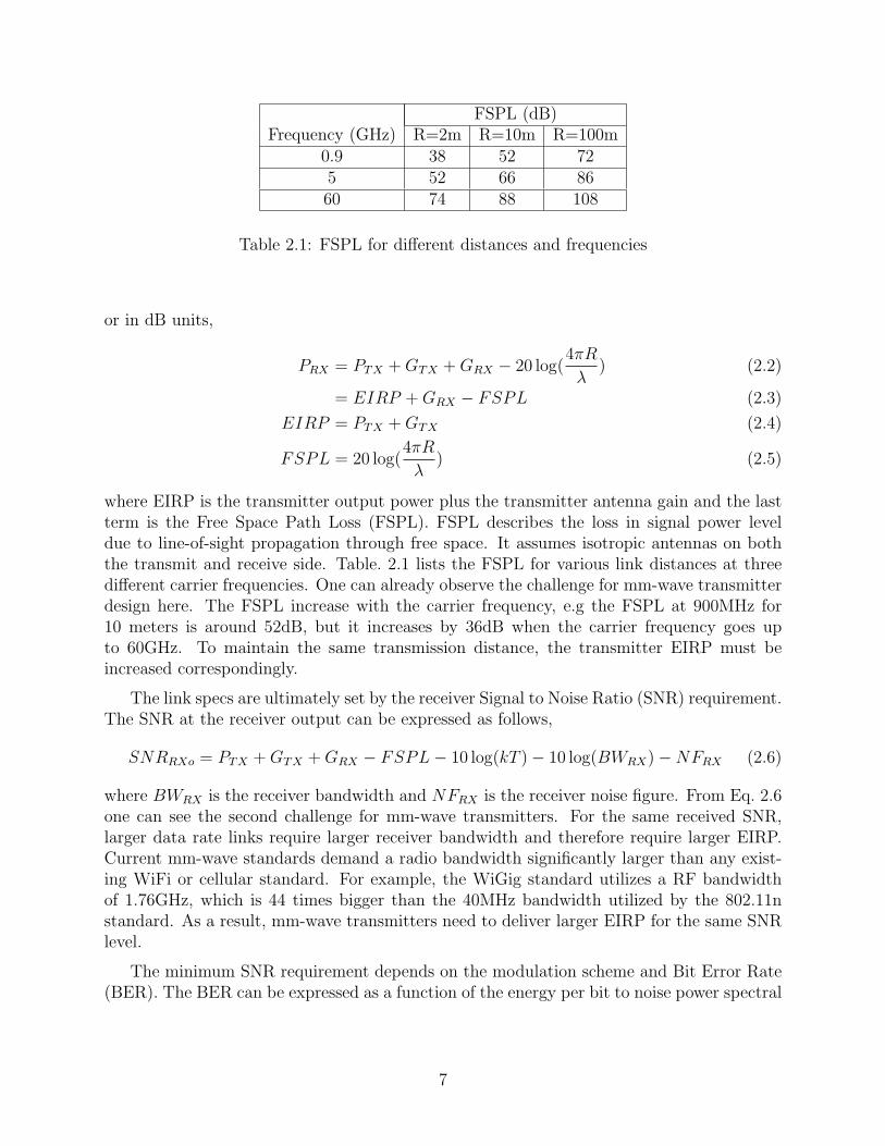
FSPL (dB)Frequency (GHz) R=2m R=10m R=100m
0.9 38 52 725 52 66 8660 74 88 108
Table 2.1: FSPL for different distances and frequencies
or in dB units,
PRX = PTX +GTX +GRX − 20 log(4πR
λ) (2.2)
= EIRP +GRX − FSPL (2.3)
EIRP = PTX +GTX (2.4)
FSPL = 20 log(4πR
λ) (2.5)
where EIRP is the transmitter output power plus the transmitter antenna gain and the lastterm is the Free Space Path Loss (FSPL). FSPL describes the loss in signal power leveldue to line-of-sight propagation through free space. It assumes isotropic antennas on boththe transmit and receive side. Table. 2.1 lists the FSPL for various link distances at threedifferent carrier frequencies. One can already observe the challenge for mm-wave transmitterdesign here. The FSPL increase with the carrier frequency, e.g the FSPL at 900MHz for10 meters is around 52dB, but it increases by 36dB when the carrier frequency goes upto 60GHz. To maintain the same transmission distance, the transmitter EIRP must beincreased correspondingly.
The link specs are ultimately set by the receiver Signal to Noise Ratio (SNR) requirement.The SNR at the receiver output can be expressed as follows,
SNRRXo = PTX +GTX +GRX − FSPL− 10 log(kT )− 10 log(BWRX)−NFRX (2.6)
where BWRX is the receiver bandwidth and NFRX is the receiver noise figure. From Eq. 2.6one can see the second challenge for mm-wave transmitters. For the same received SNR,larger data rate links require larger receiver bandwidth and therefore require larger EIRP.Current mm-wave standards demand a radio bandwidth significantly larger than any exist-ing WiFi or cellular standard. For example, the WiGig standard utilizes a RF bandwidthof 1.76GHz, which is 44 times bigger than the 40MHz bandwidth utilized by the 802.11nstandard. As a result, mm-wave transmitters need to deliver larger EIRP for the same SNRlevel.
The minimum SNR requirement depends on the modulation scheme and Bit Error Rate(BER). The BER can be expressed as a function of the energy per bit to noise power spectral
7

0 5 10 15 20 25 3010−6
10−5
10−4
10−3
10−2
10−1
100
SNR (dB)
BE
R
BPSK
QPSK
16QAM
64QAM
Figure 2.2: BER as a function of SNR
density ratio (Eb/N0),
BERBPSK = Q(
√
2Eb
N0
) (2.7)
BERQPSK = Q(
√
2Eb
N0
) (2.8)
BERM−aray−QAM =4
k(1− 1√
M)Q(
√
3k
M − 1
Eb
N0
) (2.9)
where M is the number of constellation points and k is the number of bits per symbol. Eb/N0
can be further expressed in terms of SNR,
Eb
N0
=1
k
Es
N0
=1
k
BWRX
fsSNR (2.10)
The receiver RF bandwidth is usually designed to be roughly equal to the Nyquist symbolfrequency and therefore Eq. 2.10 can be simplified to,
Eb
N0
=1
kSNR (2.11)
Using this relation, the BERs in Eqn. 2.7-2.9 can be expressed in terms of SNR directly,
BERBPSK = Q(√2SNR) (2.12)
BERQPSK = Q(√SNR) (2.13)
BERM−aray−QAM =4
k(1− 1√
M)Q(
√
3
M − 1SNR) (2.14)
8

100 101 102−50
−40
−30
−20
−10
0
10
20
Communication Distance (m)
EIR
P (
dBm
)
BPSK
QPSK
16QAM
64QAM
(a) 2.4GHz link with 40MHz RF bandwidth
100 101 1020
10
20
30
40
50
60
Communication Distance (m)
EIR
P (
dBm
)
BPSK
QPSK
16QAM
64QAM
(b) 60GHz link with 5GHz RF bandwidth
Figure 2.3: Required EIRP as a function of communication distance
9

Fig. 2.2 plots the BER as a function of SNR for BPSK, QPSK, 16QAM and 64QAMmodulation schemes. In modern wireless systems, expected BER at the radio front-endoutput is around 10−3 to 10−4 1, and therefore the minimum received SNR needs to begreater than 7dB for BPSK, 10dB for QPSK, 17dB for 16QAM and 23dB for 64QAM. As aresult, with the same receiver, higher order modulation schemes require higher transmitterEIRP. Fig. 2.3 plots the required EIRP as a function of communication distance to achievea BER of 10−3, and compares a 2.4GHz link with 40MHz RF bandwidth and a 60GHz linkwith 5GHz bandwidth. In both cases, the receiver has an isotropic antenna (GRX = 0dBi)and 5dB noise figure. Clearly, the 60GHz link requires much larger EIRP for covering thesame distance, illustrating the aforementioned challenges. Note that the EIRPs shown inFig. 2.3 represent the average values, which means transmitters need to handle peak EIRPsseveral dBs higher, depending on the PAPR of the modulation scheme.
2.2 Wireless Transmitter Architectures
Most modern wireless transmitters can be classified into two different categories 2: thesuperheterodyne3 architecture and the direction conversion architecture. Common in botharchitectures, there are four major sub-systems in the RF front-end: analog baseband, fre-quency generation, modulation and frequency conversion, and power amplification. Theanalog baseband first converts the coded baseband I/Q digital bits into continuous timeanalog signals through Digital-to-Analog-Converters (DACs), and subsequently filters theanalog signals to reject unwanted high frequency spectral contents. The filtered I/Q signalsare used to modulate a high frequency carrier signal known as the Local Oscillator (LO) sig-nal. The modulated signal is amplified to achieve required power level by the PA. The highfrequency LO signal is usually generated by a Phase-Lock-Loop (PLL) taking highly accu-rate frequency reference from a quartz crystal. In a superheterodyne transmitter (Fig. 2.4),the modulation takes place at an Intermediate Frequency (IF) which is lower than the finalRF carrier frequency. Then the modulated signal is up-converted by a mixer. There aretwo major advantages: first, since the frequency generation block only needs to synthesizea lower frequency, it can achieve lower power consumption and better phase noise perfor-mance; second, modulation at IF is more power efficient and linear, and it also reducesthe operating frequency of the calibration circuits4. However, superheterodyne transmittersneed a band-pass filter after the up-conversion mixer since the mixer produces undesiredspectral contents 2×IF frequency away from the RF carrier, which is known as the image.Image leaking through the transmitter not only reduces the desired signal power, but alsopotentially interferes with other communication links operating at the image frequency band.
1The errors are being corrected by equalizers and error decoders in the digital MODEM2Except for non-coherence detection based modulation schemes such On-Off Keying (OOK) or Frequency
Modulation (FM). These modulation schemes are less spectral efficient and the corresponding transmitterarchitecture is much simpler. In fact, they existed long before the CMOS radios.
3Sometimes simply referred to as hererodyne4This is especially true for mm-wave transmitters where high frequency blocks need proper impedance
matching and careful layout.
10

Digital
Baseband
Modem
PA
PLL /2
DAC
DAC
I-Channel
Q-Channel
cal.
To RX
0˚ 90˚
2/3 fLO
1/3 fLO
Figure 2.4: A sliding-IF superheterodyne transmitter
Digital
Baseband
Modem
PA
PLL /2
DAC
DAC
I-Channel
Q-Channel
cal.
To RX
0˚ 90˚
fLO
2fLO
Figure 2.5: A direct conversion transmitter
11

To eliminate the image problem, direction conversion architecture can be used, in whichthe modulation happens at the final RF carrier frequency. This means the image is actualthe signal itself, and therefore no filtering is required. However, one practical problem ofthe direction conversion transmitter is the VCO pulling. Since the PA output contains awideband signal around the carrier and the amplitude level is usually very large (e.g. 20dBmoutput power with 50Ω load corresponds to 3.3V of swing), the VCO oscillation frequencymay be dragged around by the parasitic feedback from the PA. A good layout that isolates thePA from the VCO reduces the pulling effect, however, it’s almost impossible to completelyblock the feedback paths from the PA since they exist everywhere: supply coupling, substratecoupling and even reflection from the package! Pulling at close-in frequencies can be correctedby the PLL, but unfortunately the PLL usually has a much lower bandwidth compared tothe data bandwidth, and therefore is not effective in reducing pulling at higher frequencies.A common solution is to synthesize a clock that is multiples of the desired LO frequency, asshown in Fig. 2.5. It’s generally much more difficult to pull a VCO running at the multiplesof the pulling signal frequency.
2.3 Power Amplifiers (The ABCDEFs)
The most power consuming block in a wireless transmitter is the power amplifier. In aWLAN transmitter, the PA usually contributes over 60% of the total power consumption[3]. As a result, the power efficiency of the PA is directly related to the battery life of mobiledevices. To quantify the PA efficiency, several efficiency measures are used. The most widelyused measures are the drain efficiency (ηD)
5 and the Power Added Efficiency (PAE). Thedrain efficiency is defined as the ratio between the useful output power Pout and the DCpower supplied to the drain of the PA device PDC ,
ηD =Pout
PDC
(2.15)
The drain efficiency tells how much power is being dissipated during the DC to AC powerconversion. The losses include power dissipation in the transistor as well as in the passivematching network. On the other hand, PAE takes into account of the additional power usedto drive the PA device and is defined as the ratio between the added power Pout − Pin andthe DC power PDC ,
PAE =Pout − Pin
PDC
(2.16)
The PAE is related to ηD by the power gain of the PA GP ,
PAE = ηD(1−1
GP
) (2.17)
The significance of the PAE measure can be understood when analyzing a cascaded chain ofsimilar amplifiers. Assume each amplifier has a drain efficiency of ηD and a power gain of
5It’s also referred to as collector efficiency in bipolar PAs
12
GP , the output power and the DC power of the nth stage are,
Pout(n) =Pout
GN−np
(2.18)
PDC(n) =1
ηD
Pout
GN−np
(2.19)
Summing the DC power of each stage, the total DC power is,
PDC =N∑
n=1
PDC(n) =Pout
ηD
1− 1GN
P
1− 1GP
(2.20)
The cascaded PAE is,
PAEcascaded =Pout(1− 1
GNP
)
Pout
ηD
1− 1
GNP
1− 1GP
= ηD(1−1
GP
) = PAE (2.21)
Therefore, the cascaded PAE is identical to the single-stage PAE. When N approaches asufficiently large number, the input power becomes negligible and the PAE represents thetotal power efficiency of the amplifier chain.
Depending on the input-output relation, power amplifiers are usually categorized as linearamplifiers and non-linear amplifiers. Within each category, multiple classes are definedaccording to the voltage and current waveforms. The following subsections will describethese different classes.
2.3.1 Linear Classes (Class-A/B/AB)
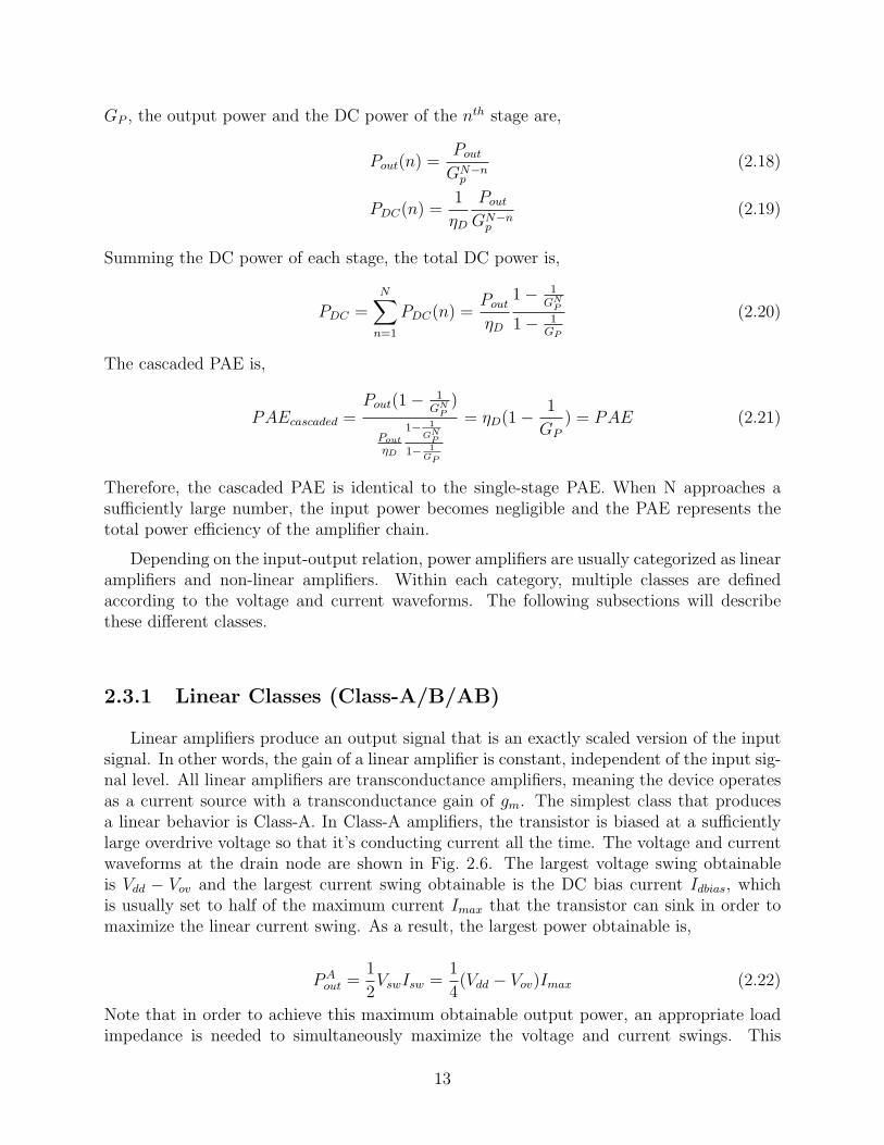
Linear amplifiers produce an output signal that is an exactly scaled version of the inputsignal. In other words, the gain of a linear amplifier is constant, independent of the input sig-nal level. All linear amplifiers are transconductance amplifiers, meaning the device operatesas a current source with a transconductance gain of gm. The simplest class that producesa linear behavior is Class-A. In Class-A amplifiers, the transistor is biased at a sufficientlylarge overdrive voltage so that it’s conducting current all the time. The voltage and currentwaveforms at the drain node are shown in Fig. 2.6. The largest voltage swing obtainableis Vdd − Vov and the largest current swing obtainable is the DC bias current Idbias, whichis usually set to half of the maximum current Imax that the transistor can sink in order tomaximize the linear current swing. As a result, the largest power obtainable is,
PAout =
1
2VswIsw =
1
4(Vdd − Vov)Imax (2.22)
Note that in order to achieve this maximum obtainable output power, an appropriate loadimpedance is needed to simultaneously maximize the voltage and current swings. This
13

optimal load impedance can be expressed as a ratio of the voltage swing and the currentswing,
RAopt = 2
Vdd − Vov
Imax
(2.23)
When the load impedance is smaller than RAopt, the amplifier becomes current limited, mean-
ing that there isn’t enough current swing to generate the maximum voltage swing. Likewise,if the load impedance is larger than RA
opt, the amplifier becomes voltage limited, meaningthat only a fraction of the current swing is sufficient to saturate the voltage swing. In bothcases, the output power decreases from PA
out. The peak drain efficiency of Class-A amplifiersis obtained when RA
opt is presented,
ηAD =PAout
PDC
=(Vdd−Vov)Imax
4VddImax
2
=Vdd − Vov
2Vdd
≈ 50% (2.24)
Class-A amplifiers have all the attractiveness except for the efficiency. 50% of the DC poweris dissipated on the transistor when the product of drain voltage and current is non-zero.In other words, the transistor dissipates power whenever there’s overlap between non-zerovoltage and current waveforms. Therefore, it’s obvious that in order to improve the efficiency,the overlapping period needs to be reduced.
A simple way to achieve this goal is to bias the transistor at the threshould voltagesuch that the transistor is conducting current during half of the cycle. Such amplifiers areknown as Class-B amplifiers, and the drain node voltage and current waveforms are shown inFig. 2.7. Since the transistor is only conducting current 50% of the time, the amount of V-Ioverlap is greatly reduced. The current going into the transistor drain becomes a half-waverectified sine, with a fundamental component of Imax
2and a DC value of Imax
π. The output
power, optimal load impedance and the drain efficiency of Class-B amplifiers can be foundin a similar way,
PBout =
1
2VswIsw =
1
4(Vdd − Vov)Imax (2.25)
RBopt = 2
Vdd − Vov
Imax
(2.26)
ηBD =PBout
PDC
=(Vdd−Vov)Imax
4π
VddImax
=π(Vdd − Vov)
4Vdd
≈ 79% (2.27)
Compared to Class-A amplifiers, Class-B amplifier has much better peak drain efficiency,but maintains the same peak output power. The disadvantage is that the amplifier becomesslightly nonlinear, due to the varying effective bias condition at the input. However, theamplifier is fundamentally considered as a linear class due to the transconductance behaviorof the device.
To improve the linearity of Class-B amplifiers, the gate bias of the transistor can beset slightly higher than the threshold voltage so that the transistor is conducting currentmore than half of the cycle, but still much less than the entire cycle. This sub-category iscalled Class-AB amplifiers. As a result, the efficiency will lie between Class-A and Class-B
14

VB
0 0.5 10
1
2
Time
Voltage /
Curr
ent
VTH
voltagecurrent
Figure 2.6: Schematics and V-I Waveforms of Class-A amplifiers
VB
VTH
0 0.5 10
1
2
3
4
Time
Voltage /
Curr
ent
voltage
current
Figure 2.7: Schematics and V-I Waveforms of Class-B amplifiers
15

amplifiers. To find the power and efficiency of Class-AB amplifiers, the current swing andDC current are first expressed as a function of the conduction angle α, defined as the totalnumber of radians in one cycle during which the transistor is conducting current,
Isw =1
2π[
α− sinα
1− cos(α/2)]Imax (2.28)
IDC =1
2π[2 sin(α/2)− α cos(α/2)
1− cos(α/2)] (2.29)
Next, the output power, optimal load impedance and the drain efficiency of Class-AB am-plifiers can be found,
PABout =
1
4π[
α− sinα
1− cos(α/2)](Vdd − Vov)Imax (2.30)
RABopt = 2π[
1− cos(α/2)
α− sinα]Vdd − Vov
Imax
(2.31)
ηABD =
PABout
PDC
=1
2
Vdd − Vov
Vdd
α− sinα
2 sin(α/2)− α cos(α/2)(2.32)
α ⊂ [π, 2π] (2.33)
2.3.2 Non-Linear Classes (Class-C/D/E/F)
Unlike linear amplifiers, non-linear amplifiers lack of amplitude linearity. They usuallyproduce significant amplitude-to-amplitude (AM-AM) and amplitude-to-phase (AM-PM)distortions. As a result, they cannot be directly used for convey amplitude modulatedsignals. However, most non-linear amplifiers are still linear in phase, and have no phase-to-phase (PM-PM) distortions. Therefore, they are often used for amplifying phase modulatedsignals such as GMSK signals. The biggest advantage of most non-linear amplifiers is thehigh drain efficiency. A linear transconductance amplifier can be turned into a non-linearamplifier by biasing the transistor below threshold voltage. Such amplifiers are known asClass-C amplifiers (Fig. 2.8). Class-C amplifiers conduct current less than half of the cycle,and have smaller window of V-I overlap. Therefore, the efficiency of Class-C amplifiers iseven higher than that of Class-B amplifiers. The expression for output power, optimal loadimpedance and efficiency of Class-C amplifiers is the same as Class-AB amplifiers, but theconduction angle is smaller than π.
PCout =
1
4π[
α− sinα
1− cos(α/2)](Vdd − Vov)Imax (2.34)
RCopt = 2π[
1− cos(α/2)
α− sinα]Vdd − Vov
Imax
(2.35)
ηCD =PABout
PDC
=1
2
Vdd − Vov
Vdd
α− sinα
2 sin(α/2)− α cos(α/2)(2.36)
α ⊂ [0, π] (2.37)
16

In theory, Class-C amplifiers can have drain efficiency as high as 100%. However, thisis achieved at zero conduction angel, which means the output power also drops to zeroaccording to Eq. 2.34. Unlike Class-AB amplifiers, Class-C amplifier has a clear tradeoffbetween output power and drain efficiency.
Due to the low output power level, Class-C amplifiers are seldom used as a stand-aloneamplifier unit6. More widely used non-linear amplifiers are switching amplifiers. In switchingamplifiers, transistors behave like switches, and it’s either in triode region or in cut-off region.This is in contrast with transconductance amplifiers in which transistors remain in saturationregion.
A switching amplifier can be constructed with an inverter which produces a square volt-age waveform. In order to extract the fundamental component, a series LC band-pass filtercan be added at the output. Such amplifiers are known as Class-D amplifiers (Fig. 2.9).Since only fundamental frequency current can flow through the filter, each of the two tran-sistors contribute half cycle of the sine current waveform. Since there’s no V-I overlap, thetheoretical peak drain efficiency is 100%. The maximum voltage and current swings are,
Vsw =2
πVdd (2.38)
Isw = Imax (2.39)
Therefore the output power, optimal load impedance and the drain efficiency can be found,
PDout =
1
πVddImax (2.40)
RDopt =
Vsw
Isw=
2
π
Vdd
Imax
(2.41)
ηDD =VswIsw
2VDCIDC
≈1πVddImax
Vdd1πImax
= 100% (2.42)
Note that the peak drain efficiency can only be achieved at very low frequency, where thetransistor capacitance is negligible. Unfortunately, the power spent charging the transistordrain node parasitic capacitance increases linearly with frequency. Besides this chargingpower loss, the parasitic capacitor also smooths the edges of the square waveform, andthereby introduces finite V-I overlap. As a consequence, Class-D amplifiers are seldom usedfor high frequency designs due to dramatically reduced efficiency.
Class-E amplifiers can absorb the transistor parasitic capacitance into an impedancetuning network while ensure non-overlapping V-I waveforms (Fig. 2.10)[4, 5]. When theswitch is off, the current flowing into the drain is zero while the drain voltage is non-zero.The voltage waveform reaches zero right before the switch is turned on, after which thedrain voltage remains zero when the transistor sinks current. Such transition behavior iscalled Zero Voltage Switching (ZVS). ZVS not only ensures non-overlapping V-I waveforms,but also avoids charge loss when the switch turns on. In fact, Class-E amplifiers satisfy notonly ZVS but also Zero derivative Voltage Switching (ZdVS), meaning the derivative of the
6It’s often used in conjunction with other amplifiers for efficiency enhancement, such as Doherty amplifiers
17

0 0.5 10
1
2
3
4
5
6
7
Time
Voltage /
Curr
ent
VB
VTH voltage
current
Figure 2.8: Schematics and V-I Waveforms of Class-C amplifiers
0 0.5 10
1
2
3
4
Time
Voltage /
Curr
ent
voltage
current
Figure 2.9: Schematics and V-I Waveforms of Class-D amplifiers
18

voltage waveform at the time instant when the switch turns on is also zero. This propertysignificantly reduces the efficiency sensitivity due to the passive component variations. Thetypical Class-E implementation is shown in Fig. 2.10. A series LC filter is used so that theload impedance is only seen at the fundamental frequency. As a result, the transistor seesinductive load impedance at the fundamental frequency while it only sees the parasitic draincapacitor at all harmonics. An inductor choke is used to provide the DC current path. Thederivation for the required tuning impedances is skipped here, since it’s given in multipleliteratures [6, 7, 8].
PEout ≈ VDCIDC =
1
FPI
VddImax =1
2.86VddImax (2.43)
ZEC,opt = FPIFC
Vdd
Imax
= 8.985Vdd
Imax
(2.44)
REopt = 0.1836ZE
C,opt = 1.65Vdd
Imax
(2.45)
XEopt = 1.152RE
opt = 1.9Vdd
Imax
(2.46)
FPI = 2.86 (2.47)
FC = π (2.48)
ηED ≈ 100% (2.49)
The final amplifier class in alphabetical order is Class-F. Class-F amplifiers are con-structed based on Class-B amplifiers. In order to further improve the efficiency of Class-Bamplifiers beyond 79% while not sacrificing the output power, odd harmonics can be addedto the voltage waveform. The addition of the odd harmonics shapes the voltage waveformfrom a sine to a square, and thus reducing the V-I overlap. By increasing the number ofharmonics, the efficiency can approach 100% eventually. To implement this idea, a bank offilters need to be inserted in series at the amplifier output to present Open Circuit (O.C.)impedance to the transistor at odd harmonics to enrich the odd harmonic content in thedrain voltage waveform while a low-pass filter is needed at the output to eliminate all theeven order harmonics (Fig. 2.11). When sufficient harmonics are added, the waveform re-sembles that of Class-D amplifiers. The output power, optimal impedance and efficiency ofClass-F amplifiers are,
P Fout =
1
2
4
πVdd
1
2Imax =
1
πVddImax (2.50)
RFopt =
Vsw
Isw=
8
π
Vdd
Imax
(2.51)
ηFD =VswIsw
2VDCIDC
≈1πVddImax
Vdd1πImax
= 100% (2.52)
Similar to Class-D amplifiers, the efficiency of Class-F amplifiers is also degraded by theparasitic capacitance at the transistor drain node. In addition, it requires large number offilters for harmonic generation which introduces insertion loss. As a result, the beauty ofClass-F amplifiers is usually lost in implementation.
19

voltagecurrent
C
X
0 0.5 10
1
2
3
4
Time
Voltage /
Curr
ent
Figure 2.10: Schematics and V-I Waveforms of Class-E amplifiers
0 0.5 10
1
2
3
4
Time
Voltage /
Curr
ent
VB
VTH
voltagecurrent
Increasing N
O.C. 3rd
Harmonic
O.C. 5th
Harmonic
O.C. Nth
Harmonic
S.C. All
Harmonics
Figure 2.11: Schematics and V-I Waveforms of Class-F amplifiers
20

2.4 The Extended Class-E/F Family
As discussed in the previous section, Class-E amplifiers have ZVS waveform character-istic. In fact, there are numerous impedance tuning networks which can produce the ZVSwaveform. It was not until recently that the relation between different impedance tuningnetworks was well discovered. In [8], it’s summarized that many of the ZVS tuning networksbelong to the Class-E/F family. Different members of the family correspond to differentharmonic impedances, with Class-E and Class-F−1 being the two extremes: Class-E hasno harmonic impedance tuning while Class-F−1 has impedance tuning at all harmonics.The essential rule of the Class-E/F harmonic tunings in [8] is as follows: the effective loadimpedance needs to be open circuit at even harmonics but short circuit at odd harmonics.Table. 2.2 shows examples of some Class-E/F tunings in terms of harmonic impedance.
It’s also shown in [8] that the power, efficiency and gain of a Class-E/F amplifier can beexpressed in terms of a set of technology dependent parameters such as transistor resistanceand capacitance, defined in Table. 2.3, and also a set of technology independent parameterscalled the waveform figures of merit. The waveform figures of merit are determined by thecombination of the harmonic load impedances and are unique to each tuning class. Theyare defined as follows,
FV =Vpk
VDC
(2.53)
FI =IRMS
IDC
(2.54)
FPI =IpkIDC
(2.55)
FC =VDCIDC
V 2DC/ZC
(2.56)
FV is the ratio between the peak and DC voltages. FI is the ratio between the RMS andDC current. FPI is the ratio between the peak and DC current. FC is the ration betweenthe DC power and the reactive power stored on the drain capacitor. Under the conditionthat the transistor is sized to be largest possible given the capacitance constraint, the drainefficiency, power gain and PAE can be expressed as follows,
ηEFD = 1− (F 2
I FC)2πf0(roncout) (2.57)
GEF = ηEFD (
coutV2bk
pin)(FC
F 2V
)2πf0 (2.58)
PAEEF = (1− 1
GEF)ηEF
D (2.59)
Note that here the loss due to the transistor finite on-resistance is taken into account.
The original Class-E/F family in [8] only considers open or short load for harmonicterminations, however, it turns out ZVS waveform can be achieved using arbitrary harmonic
21

Tuning f0 2f0 3f0 4f0 5f0 6f0 7f0
E
CXopt R
opt C C C C C C
E/F2
CXopt R
opt
Open
C C C C C
E/F3
CXopt R
opt C
Short
C C C C
E/F2,3
CXopt R
opt
Open Short
C C C C
E/F2,3,4,5
CXopt R
opt
Open Short Open Short
C C
F−1
Ropt
Open Short Open Short Open Short
Table 2.2: The harmonic impedance specifications of several original Class-E/F tunings
22
Vbk Breakdown voltage (V )ron normalized transistor on-resistance (Ωm)cout normalized transistor output capacitance (F/m)cin normalized transistor input capacitance (F/m)pin normalized input driving power (W/m)
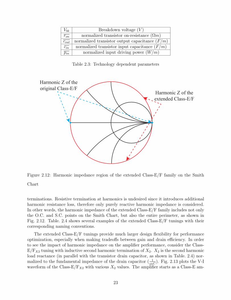
Table 2.3: Technology dependent parameters
Harmonic Z of the
original Class-E/F Harmonic Z of the
extended Class-E/F
Figure 2.12: Harmonic impedance region of the extended Class-E/F family on the Smith
Chart
terminations. Resistive termination at harmonics is undesired since it introduces additionalharmonic resistance loss, therefore only purely reactive harmonic impedance is considered.In other words, the harmonic impedance of the extended Class-E/F family includes not onlythe O.C. and S.C. points on the Smith Chart, but also the entire perimeter, as shown inFig. 2.12. Table. 2.4 shows several examples of the extended Class-E/F tunings with theircorresponding naming conventions.
The extended Class-E/F tunings provide much larger design flexibility for performanceoptimization, especially when making tradeoffs between gain and drain efficiency. In orderto see the impact of harmonic impedance on the amplifier performance, consider the Class-E/FX2 tuning with inductive second harmonic termination of X2. X2 is the second harmonicload reactance (in parallel with the transistor drain capacitor, as shown in Table. 2.4) nor-malized to the fundamental impedance of the drain capacitor ( 1
ω0C). Fig. 2.13 plots the V-I
waveform of the Class-E/FX2 with various X2 values. The amplifier starts as a Class-E am-
23

Tuning f0 2f0 3f0 4f0 5f0 6f0 7f0
E
CXopt R
opt C C C C C C
E/FX2
CXopt R
opt X2
C C C C C C
E/FX2,X3
CXopt R
opt X2
C X3
C C C C C
Table 2.4: The harmonic impedance specifications of several extended Class-E/F tunings
0 0.5 1
1
2
3
4
Time
Voltage /
Curr
ent
0 0.5 10
1
2
3
4
Time
Voltage /
Curr
ent
0 0.5 10
1
2
3
4
Time
Voltage /
Curr
ent
0 0.5 10
1
2
3
4
Time
Voltage /
Curr
ent
0 0.5 10
1
2
3
4
5
Time
Voltage /
Curr
ent
0 0.5 1
−8
−6
−4
−2
0
2
4
6
8
10
Time
Voltage /
Curr
ent
X2=106 X
2=1 X
2=0.75
X2=0.5 X
2=0.391 X
2=0.32
Figure 2.13: V-I Waveforms of the Class-E/FX2 tunings with various X2 values
24

10−1
100
101
102
3.5
3.55
3.6
3.65
3.7
3.75
3.8
FV
X2
10−1
100
101
102
1.4
1.5
1.6
1.7
1.8
FI
X2
10−1
100
101
102
0
1
2
3
4
FC
X2
10−1
100
101
102
2
2.5
3
3.5
4
4.5
5
FPI
X2
Figure 2.14: Waveform FoM of Class-E/FX2 tunings as a function of X2
plifier when X2 is infinity. When X2 decreases, stronger second harmonic content is presentin the current waveform. When X2 reaches 0.5, the amplifier becomes Class-E/F2, sincethe load reactance cancels out the reactance of the drain capacitor, presenting an overallO.C. at the second harmonic. Further decreasing X2 keeps enriching the second harmoniccontent until the minimum instantaneous current reaches zero. Since it’s undesired to havereverse direction current through the transistor, there’s a lower limit on the X2 value. ForClass-E/FX2, the minimum X2 is 0.391. Based on V-I waveforms, the four waveform figuresof merit can be calculated. Fig. 2.14 plots FV , FI , FC and FPI as a function of X2. WhenX2 decreases from infinity (no second harmonic tuning), FV increases while FC decreases,meaning larger peak to average voltage ratio and larger drain capacitance tolerance. LowFC is desired from drain efficiency point of view since larger transistor size can be used toreduce the on resistance loss. On the other hand, the behavior of both FI and FPI is non-monotonic. Both FI and FPI decreases initially until it reaches the minimum value and theystart to climb back up. The minimum is obtained when X2 is 0.5. Since low FI is desired for
25

10−1
100
101
102
0.94
0.95
0.96
0.97
0.98
0.99
DE
X2
10−1
100
101
102
6
7
8
9
10
11
12
13
14
G (dB)
X2
10−1
100
101
102
0.76
0.78
0.8
0.82
0.84
0.86
0.88
0.9
0.92
PAE
X2
(a) f0 = 2.4GHz
10−1
100
101
102
0.8
0.82
0.84
0.86
0.88
0.9
0.92
0.94
0.96
DE
X2
10−1
100
101
102
6
7
8
9
10
11
12
13
14
G (dB)
X2
10−1
100
101
102
0.72
0.74
0.76
0.78
0.8
0.82
0.84
PAE
X2
(b) f0 = 10GHz
10−1
100
101
102
0.35
0.4
0.45
0.5
0.55
0.6
0.65
0.7
0.75
DE
X2
10−1
100
101
102
6
7
8
9
10
11
12
13
14
G (dB)
X2
10−1
100
101
102
0.35
0.4
0.45
0.5
0.55
0.6
0.65
0.7
PAE
X2
(c) f0 = 60GHz
Figure 2.15: ηD, Gp and PAE of Class-E/FX2 amplifiers as a function of X2
26

efficiency, X2 = 0.5 gives the best FI value. Note that with X2 = 0.5, the tuning becomesClass-E/F2.
Based on a typical 65nm CMOS technology, the drain efficiency, power gain and PAE ofClass-E/FX2 amplifiers can be plotted as a function of X2 for different operating frequencies,as shown in Fig. 2.15. There’s a clear tradeoff between drain efficiency and power gain:decreasing X2 decreases the product F 2
I FC and therefore improves the drain efficiency; butdue to decreased FC , or equivalently increased transistor size, larger input power is neededwhich leads to reduced power gain. The optimal PAE point depends on not only technologyparameters, but also the operating frequency. At 2.4GHz, the optimal PAE is obtainedwhen X2 is roughly 2. At 10GHz, the optimal PAE is obtained when X2 is around 0.6.Finally at 60GHz, the optimal PAE is obtained when X2 is around 0.45. Intuitively, thedecreasing optimal X2 value is caused by the fact that ηD drops with increasing frequency,and therefore larger transistor sizes are needed to reduce the on resistance loss, which meanslower FC value is desired.
2.5 High Frequency Challenges
CMOS technology scaling has dramatically improved the transistor speed, as a result,significant progress has been achieved in integrating many of the mm-wave circuit blocks.However, mm-wave power amplifiers still face many design challenges. Fig. 2.16 shows aperformance survey of the state-of-the-art CMOS PA over a wide frequency range. A cleartrend can be observed here: both output power and efficiency drop with increasing operatingfrequency. This trend can be explained by multiple reasons. Since the product of transistorft and breakdown voltage is kept roughly constant during technology scaling, the breakdownvoltage reduces as ft improves. The thin oxide breakdown voltage is around 15MV/cm, andwith oxide thickness in the order of 1nm, the breakdown voltage is usually around 1V. Thismeans all the mm-wave devices need to operate from a very low supply voltage, which directlyaffect the PA output power since power is proportional to the voltage square. To delivermore power with the same supply voltage, the transistor need to deliver more current andtherefore it needs to see a smaller load impedance. This means an impedance transformationnetwork is needed at the PA output. However, the insertion loss of the matching networkis inversely proportional to the impedance transformation ratio, and larger desired outputpower translates into larger insertion loss in the matching network. The result is that witha simple LC impedance transformation network, there is a limit on the obtainable outputpower [9]. To make things worse, technology scaling not only shrinks the copper metalthickness but also reduce the distance between top metal layer and the silicon substrate,thus reducing the Quality factor (Q factor) of on-chip passives. It’s also shown in [9] thatthe maximum obtainable output power is proportional to the square of the Q factor.
The main factor that contributes to the reduced efficiency at high frequency is the reducedtransistor power gain. For Class-A/AB amplifiers, the drain efficiency of mm-wave PA isin fact very comparable to their low frequency counterpart, however, since the Maximum
27

0
5
10
15
20
25
30
35
40
0.1 1 10 100 1000
Ou
tpu
t P
ow
er
[dB
m]
Frequency [GHz]
CMOS
(a) Output Power
0
10
20
30
40
50
60
70
80
0.1 1 10 100 1000
Eff
icie
ncy
[%
]
Frequency [GHz]
CMOS
(b) Efficiency
Figure 2.16: A survey of CMOS PA performance
Stable Gain (MSG) drops with increasing frequency, more power is needed to drive the PA.At 60GHz for example, a single stage PA can only provide 5-6dB power gain after includingthe passive loss. According to Eq. 2.16, the PAE can be much lower than the drain efficiencydue to the low power gain. Driver stages are usually used to boost the overall gain of thePA chain, but it’s also shown in Eq. 2.21 that cascading gain stages do not affect the PAE7.
7In practice, adding driver stages slightly improves the overall PAE since the drive stages are impedancematched for maximum power gain, and therefore exhibit a different ηD and Gp profile than the last PAstage.
28

Chapter 3
Linear Transmitter
Most higher order single carrier modulation schemes such as QAM require a linear analogfront-end to preserve the relative amplitude information. Even seemingly constant envelopesignals such as Nyquist rate BPSK has a non-zero PAPR after low-pass filtering. As a result,linear transmitters are widely used today. To cover longer communication distance, larger PAoutput power is desired to increase the transmitter EIRP. In addition, Orthogonal FrequencyDivision Multiplexing (OFDM) technique is widely used in wireless communication today tomitigate the multi-path effect. One downside of such technique is the large signal PAPR.With increased signal PAPR, the peak output power level must be boosted accordingly,presenting a further challenge. This chapter discusses techniques for increasing the outputpower level of the linear class PAs while maximizing the efficiency.
3.1 Power Combining Techniques
As shown in [9], with a LC type of impedance transformation network, the output powerof a single transistor PA cannot be increased indefinitely due to increased insertion loss.Therefore the only way to further increase the output power is to combine power from mul-tiple transistors through a power combiner. A very intuitive idea is to use direct currentsumming (Fig. 3.1a). The advantage of such an approach is simple in implementation andlow insertion loss. However, since each transistor sees N times higher impedance than theload where N is the number of combined branches, additional impedance matching networkis needed in order to increase the total output power. As a result, the maximum obtain-able output power stays roughly the same as a single transistor PA. The only benefit isthat since each transistor is much smaller, transistor internal wiring loss can be reduced.Current summing based mm-wave PAs have shown limited output power, typically below14dBm at 60GHz [10, 11]. Another well-known approach is Wilkinson combiners. Unlike
29
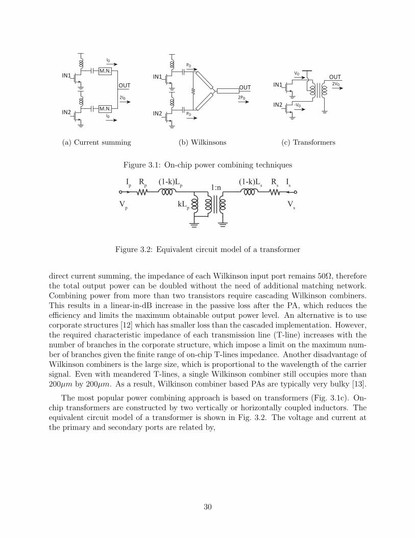
M.N.
M.N.
IN1
IN2
OUT
I0
I0
2I0
(a) Current summing
IN1
IN2
P0
OUT
P0
2P0
(b) Wilkinsons
IN1
IN2
V0OUT
2V0
-V0
(c) Transformers
Figure 3.1: On-chip power combining techniques
1:n(1-k)L
p
kLp
Rp
(1-k)LsRs
Vp
Ip
Is
Vs
Figure 3.2: Equivalent circuit model of a transformer
direct current summing, the impedance of each Wilkinson input port remains 50Ω, thereforethe total output power can be doubled without the need of additional matching network.Combining power from more than two transistors require cascading Wilkinson combiners.This results in a linear-in-dB increase in the passive loss after the PA, which reduces theefficiency and limits the maximum obtainable output power level. An alternative is to usecorporate structures [12] which has smaller loss than the cascaded implementation. However,the required characteristic impedance of each transmission line (T-line) increases with thenumber of branches in the corporate structure, which impose a limit on the maximum num-ber of branches given the finite range of on-chip T-lines impedance. Another disadvantage ofWilkinson combiners is the large size, which is proportional to the wavelength of the carriersignal. Even with meandered T-lines, a single Wilkinson combiner still occupies more than200µm by 200µm. As a result, Wilkinson combiner based PAs are typically very bulky [13].
The most popular power combining approach is based on transformers (Fig. 3.1c). On-chip transformers are constructed by two vertically or horizontally coupled inductors. Theequivalent circuit model of a transformer is shown in Fig. 3.2. The voltage and current atthe primary and secondary ports are related by,
30

[
Vp
Vs
]
=
[
jωLp +Rp −jωMjωM −jωLs −Rs
] [
IpIs
]
(3.1)
M = k√
LpLs (3.2)
n =
√
Ls
Lp
(3.3)
The Q-factors of the primary and secondary inductors are defined as,
Qp =ωLp
Rp
(3.4)
Qs =ωLs
Rs
(3.5)
It’s proven in [9, 14] that the maximum efficiency of a transformer only depends on Qp, Qs
and k,
ηmax =1
1 + 2QpQsk2
+ 2√
1QpQsk2
(1 + 1QpQsk2
)(3.6)
This maximum efficiency is obtained when the following condition is met,
ωLs =1
ωCL,series
(3.7)
ωLp =α
1 + α2
RL
n2(3.8)
α =1
√
1Q2
s+ Qp
Qsk2
(3.9)
Clearly, larger Q-factor and k-factor lead to higher efficiency or equivalently lower insertionloss. One important observation here is that the efficiency is independent of the impedancetransformation ratio (≈ n2 = Ls
Lp). This effectively means the tradeoff between output power
and matching network loss is eliminated, and higher output power level can be achievedwithout incurring larger passive loss.
In Fig. 3.1c, the transformer combines the signals from a push-pull pair (pseudo-differential pair) through voltage stacking. This effectively means each transistor sees halfof the load impedance, and maximum output power can be delivered by each transistor istwice that of a single transistor PA. Combining the power of two such transistors, the totaloutput power is four times larger. Transformers offer additional advantages such as built-indifferential to single-ended signal conversion and convenient DC bias through center tap ina multi-stage design. Mm-Wave PAs based on such transformers have shown output powerbeyond 12dBm with decent efficiency [15, 16, 17].
31
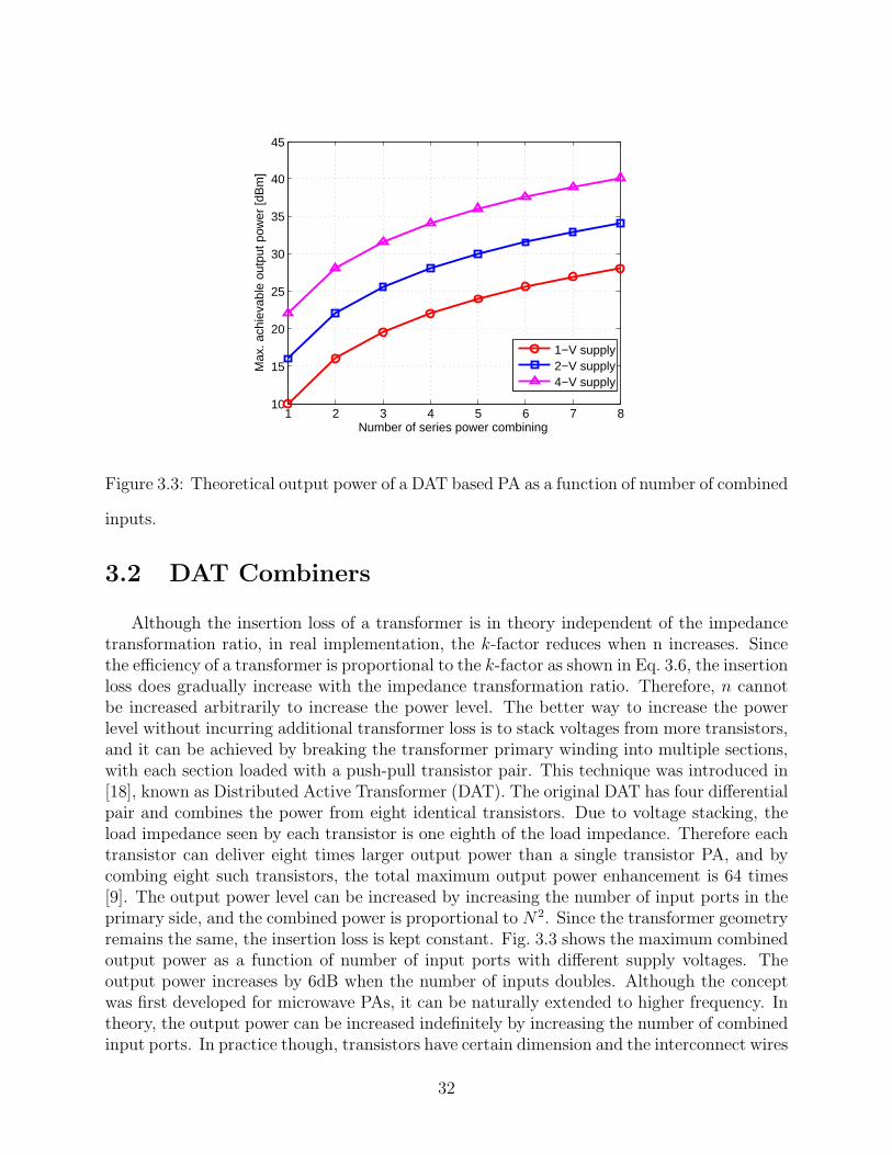
1 2 3 4 5 6 7 810
15
20
25
30
35
40
45
Number of series power combining
Max
. ach
ieva
ble
outp
ut p
ower
[dB
m]
1−V supply2−V supply4−V supply
Figure 3.3: Theoretical output power of a DAT based PA as a function of number of combined
inputs.
3.2 DAT Combiners
Although the insertion loss of a transformer is in theory independent of the impedancetransformation ratio, in real implementation, the k-factor reduces when n increases. Sincethe efficiency of a transformer is proportional to the k-factor as shown in Eq. 3.6, the insertionloss does gradually increase with the impedance transformation ratio. Therefore, n cannotbe increased arbitrarily to increase the power level. The better way to increase the powerlevel without incurring additional transformer loss is to stack voltages from more transistors,and it can be achieved by breaking the transformer primary winding into multiple sections,with each section loaded with a push-pull transistor pair. This technique was introduced in[18], known as Distributed Active Transformer (DAT). The original DAT has four differentialpair and combines the power from eight identical transistors. Due to voltage stacking, theload impedance seen by each transistor is one eighth of the load impedance. Therefore eachtransistor can deliver eight times larger output power than a single transistor PA, and bycombing eight such transistors, the total maximum output power enhancement is 64 times[9]. The output power level can be increased by increasing the number of input ports in theprimary side, and the combined power is proportional to N2. Since the transformer geometryremains the same, the insertion loss is kept constant. Fig. 3.3 shows the maximum combinedoutput power as a function of number of input ports with different supply voltages. Theoutput power increases by 6dB when the number of inputs doubles. Although the conceptwas first developed for microwave PAs, it can be naturally extended to higher frequency. Intheory, the output power can be increased indefinitely by increasing the number of combinedinput ports. In practice though, transistors have certain dimension and the interconnect wires
32

+ - + - + - + -
+-
+-
+-
+-
+-
+-
+-
+-
+-+-+-+-
+
-Vout
1 2
N
N-1
Figure 3.4: Increase the number of inputs to the limit.
also contribute to the total inductance of the primary winding. One can keep increasing thenumber of input ports until the point that the transistor lateral dimension is comparable tothe length of the inductor slab (Fig. 3.4). At this point, there’s no room on the primarywinding perimeter to accommodate additional transistors. Further increasing the number ofinput ports does not improve the output power. In fact this limit can be derived based ona particular process (65nm CMOS is used for all the following derivation).
For a single-turn 1:1 transformer driven by a single transistor, the load impedance forthe transistor is untransformed (50Ω). Based on Eq. 2.23, the optimal bias current for thetransistor is equal to the supply voltage and load impedance ratio,
Ib,opt =Imax
2=
Vdd
RL
(3.10)
Vov is neglected for simplicity. For 1-V supply, Ib,opt is 20mA. In a typical 65nm CMOSprocess, the current-density iden for maximum ft is around 0.5mA/µm. Therefore, 40µmdevice size is needed and this corresponds to roughly 40fF of output capacitance (cout =1fF/µm). The inductance needed to resonate out this capacitance is around 176pH at60GHz. This sets the basic requirement of the PA and the transformer when the numberof input is unity. Every time the number of input ports doubles, the load impedance seenby each transistor drops by half and therefore each transistor size needs to be doubledfor maximizing the voltage swing. This means the inductance needed for each transistor ishalved while the total loop inductance remain constant. Assuming a square shape single-turn
33

inductor, the inductance can be expressed in terms of the diameter as follows:
L = 0.2πD × 1.27(ln(2.07
β) + 0.18× β + 0.03× β2) (3.11)
where D is the diameter and β is the filling factor and is equal to 0.0833 for the squareshape. Rearranging the terms,
D =L
0.2π × 1.27(ln(2.07β) + 0.18× β + 0.03× β2)
(3.12)
For N numbers of inputs, the size of each single transistor needs to be,
W0 = NIb,optiden
(3.13)
On the other hand, the maximum lateral dimension allowed on one side of each transistoris,
l0,max =πD
N(3.14)
In a typical 65nm CMOS process, each finger extends about 0.25µm including gate, sourceand drain area. As a result, the maximum number of finger allowed to fit in l0,max is,
Nfinger,max =l0,max
lfinger=
l0,max
0.25µm(3.15)
Since the transistor size is set by the number of fingers and the finger width together, onecan always increase the finger width to meet the device requirement in (3.13). However,increasing the finger width increases the gate resistance and therefore reduces the transistorgain. This imposes another constraint. The maximum power gain of a transistor is,
Gmax =1
4(ωt
ω0
)2rorg
(3.16)
=1
4(ωt
ω0
)2(rorg)(
1
Wfinger
)2 (3.17)
where ro and rg are the normalized output resistance and input gate resistance. Since ro isinversely proportional to finger width Wfinger while rg is proportional to Wfinger, the ratio ofro to rg is inversely proportional to the square of Wfinger. In order to maintain a minimumgain of G, the Wfinger must not exceed a certain value,
Wfinger,max =1
4(ωt
ω0
)2rorg
1
G(3.18)
This sets an upper limit on the size of each transistor. When this upper limit reaches theoptimal transistor size obtained in Eq. 3.13, the maximum number of combining has beenreached.
Nfinger,max ×Wfinger,max ≥ W0 (3.19)
πD
N
1
0.25µm
1
4(ωt
ω0
)2rorg
≥ NIb,optiden
(3.20)
34

20 30 40 50 60 70 80 90 10022
24
26
28
30
32
34
36
38
40
42
Frequency [GHz]
Max.
limit o
f com
bin
ed o
utp
ut
pow
er
[dB
m]
Figure 3.5: Maximum total combined output power
The only unknown here is the number of combined inputs N , therefore it can be solved,
Nmax =
√
πD1
lfinger
1
4(ωt
ω0
)2rorg
idenIb,opt
(3.21)
Fig. 3.5 and Fig. 3.6 plot the maximum limit on the combined output power and thenumber of inputs as a function of frequency for a minimum power gain of 3dB. Note that thisis the absolute maximum achievable power without considering additional loss from passives.The frequency dependence originates from the fact that larger inductance is needed fortuning out the same capacitance at lower frequency and therefore larger inductor perimeteris allowed to fit more transistors. In practice, different inductor/transformer geometry willlead to slightly different results due to different filling factor β. Fig. 3.7 shows the total tuninginductance as a function of the operating frequency. One thing to point out here is that atlower frequency an explicit capacitor needs to be placed to reduce the tuning inductance.For example, an inductance of 1.6nH is needed for a 20GHz DAT and it’s very difficult todesign such a large inductor with Self Resonance Frequency (SRF) beyond 20GHz.
3.3 A 60GHz DAT Power Amplifier
Based on the previous analysis, a DAT based 60GHz PA is implemented in 65nm CMOS.The detailed design methodology for both the actives and the passives, as well as the mea-surement results are discussed in this section.
35

20 30 40 50 60 70 80 90 1000
5
10
15
20
25
30
35
Frequency [GHz]
Max.
No.
of
DA
T inputs
Figure 3.6: Maximum number of DAT inputs
20 30 40 50 60 70 80 90 1000
200
400
600
800
1000
1200
1400
1600
Frequency [GHz]
Tota
l tu
nin
g inducta
nce [
pH
]
Figure 3.7: Total tuning inductance of the transformer
36

3.3.1 Design Procedure
In Fig. 3.6, the maximum number of DAT inputs at 60GHz is eight, based on a targetpower gain of 3dB. Unfortunately such low gain is not very practical since it requires sig-nificant driver power and reduces the PAE. Instead the design of the last stage targets apower gain of at least 6dB. This reduces the number of DAT inputs to four. The proposedcombiner is shown in Fig. 3.8. The primary side of the transformer combiner has two pairsof differential excitation ports located on the opposite sides of the metal winding while thesecondary side is the same as the standard transformer. The two pairs of differential portsare excited in such a way that the AC current circulates in the primary winding and inducesthe magnetic flux for the secondary winding while the center points of the two half-octagontraces provide convenient DC access. Since the voltage swings are effectively stacked, theimpedance seen at each input port is one quarter of the load. Consequently, this structurehas a voltage enhancement ratio of 4 and a power enhancement ratio of 16.
Two of the most critical design aspects of the transformer combiner are the insertion lossand the input impedance. As shown in Eq. 3.6, the insertion loss is mainly determined bythe k factor and the inductor Q factor. A vertical broadside coupled structure with primarywinding on the top and secondary winding on the bottom is used and a coupling factor of0.87 is achieved at 60GHz. The thin metals in digital CMOS processes usually limit theachievable Q factor of on-chip inductors. In this design, the aluminum capping layer, whichis usually used to cover the copper bondpads, is strapped together with the top copper layerto form the primary winding. The aluminum capping layer has a thickness of 1.2µm whilethe top two copper layers have the same thickness of 0.9µm. By forming a much thickerprimary metal winding, the Q factor is improved by 50%, reaching 15.5 at 60GHz. Theinsertion loss of the combiner is further evaluated as a function of transformer radius andtrace width using EM simulators. Fig. 3.9 shows the combiner loss as a function of thetransformer dimensions. The optimal insertion loss is achieved when metal trace width isgreater than 15µm and the radius is between 25µm to 30µm. However, the design rule limitsthe maximum trace width to 12µm. Therefore the metal trace width should always to be setto this maximum limit. The lowest insertion loss under this constraint is around 0.65dB.
On the other hand, the input impedance of the transformer must be taken into accountwhen deciding the physical dimensions. Since the input susceptance is a strong function ofthe transformer radius, the transformer size is determined mainly by the transistor outputcapacitance. However, the transistor size also depends on the load resistance presented by thetransformer. As a result, several iterations are needed to find the optimal size combinationof the transistor and the transformer. This iterative process starts with an estimate of theload resistance at each input port, which is roughly one quarter of the load (Rl = 12.5Ω).Optimal bias current Ib,opt can be calculated based on Rl. With 1V supply and 200mVVov, Ib,opt is around 64mA. 200mV is chosen to maximize the fmax of the transistor. Withcurrent density of 0.5mA/µm, the required transistor size is roughly 130µm. A load-pullsimulation is performed on the device to determine the optimal load impedance for outputpower, and a transformer size can be chosen based on the required load impedance. Sucha process can be repeated in order to find the optimal active-passive combination. Notethat the optimal combination may be different for different goals such as maximizing the
37

Figure 3.8: Quad-input 60GHz DAT Combiner
0.6
0.6
0.6
0.650.65
0.65
0.65
0.65
0.70.7
0.7
0.7
0.70.7
0.75
0.75
0.750.75
0.8
0.8
0.8
0.80.8
0.85
0.85
0.85
0.850.85
0.9
0.9
0.90.9
0.95
0.950.95
0.95
1
11 1
Metal Trace Width (um)
Tra
nsfo
rmer
Radiu
s (
um
)
Insertion Loss Contour
5 7.5 10 12.5 15 17.5 2010
15
20
25
30
35
40
Figure 3.9: Insertion loss of the quad-input DAT combiner
38

Figure 3.10: Load-pull of a 140µm transistor
10 15 20 25 30 35 402
3
4
5
6
7
Transformer Radius (um)
Input
Conducta
nce
10 15 20 25 30 35 40−16
−12
−8
−4
0
4
Input
Suscepta
nce
Transformer Radius (um)
W=5um
W=10um
W=15um
W=20um
W=5um
W=10um
W=15um
W=20um
Figure 3.11: Input susceptance and conductance of the quad-input DAT combiner
39

140/0.06
140/0.0670/0.06
S
G
G
S
G
G
74Ω
335fF
Input Matching
Power SplitterDC
DC
+
+
-
-
Figure 3.12: Schematic of the three stage 60GHz PA.
output power or maximizing the efficiency. In this design, maximizing output power is usedas the main criteria. The final device size is set to 140µm, with the load-pull result shownin Fig. 3.10. The optimal normalized admittance is roughly 3.3− 3.3jΩ. Fig. 3.11 plots theinput susceptance and input conductance of the DAT combiner, with the optimal insertionloss region highlighted in yellow. 28µm radius and 12µm trace width are chosen with aninsertion loss of 0.63dB. Note that the actual load conductance is set slightly higher thanthe optimal value from loadpull as a compromise for lower transformer insertion loss.
Characterization of power transistor behaviors at mm-wave frequencies is important toensure the PA performance. A test chip with a stand-alone 140µm power transistor wasfabricated and two port S-parameters were measured up to 110GHz for different bias points.A simple wrap-around model with lumped inductors and resistors are used to achieve betterdevice π-model fitting at mm-wave frequencies.
Fig. 3.12 shows the complete schematic of the three-stage PA. A power splitter is neededpreceding the output stage in order to feed two differential pairs and the same transformercombiner structure is once more utilized with the inputs and outputs swapped to performthe task. Due to the large mismatch between the input conductance of the output stageand the output conductance of the driver stage, an extra matching network is required tocompensate the limited conductance transformation range of 1:1 transformers. To accomplish
40

this goal, two pairs of differential strip-lines are inserted between the transformer splitterand the output differential pairs. These strip-line pairs also conveniently cover the geometricdistance of the transistors separated by the transformers. A similar conductance mismatchat the input of the PA is solved by adding a series differential inductor to the transformer.To ensure the PA stability, a parallel RC combination is added to introduce resistive loss atlower frequencies [15].
3.3.2 CW Measurement Results
The PA was fabricated in a 1V 65nm GP 1P7M digital CMOS process. The measuredS-parameters are shown in Fig. 3.13. With 1V supply, the PA achieves a power gain of20.2dB and a 3-dB bandwidth of 9GHz (56GHz to 65GHz). The amplifier is unconditionallystable over the entire measured frequency range with stability factor greater than unity.The measured S-parameters are compared to the simulation results based on pre-measuredtransistor S-parameters. It can be observed that the measurement results are very close tothe simulation.
The 60GHz power measurement results are shown in Fig. 3.14. With 1V supply voltage,the measured 1dB gain compressed output power P1dB is 15dBm and the saturated outputpower PSAT is 18.6dBm. The measured peak PAE is 15.1% and the peak drain efficiencyis 16.4%. At the saturated output power level, the amplifier still has 11dB of power gain,which significantly relieves the design of the preceding block. The large signal performance isalso measured over the IEEE 802.15.3c band. As shown in Fig. 3.15, the PA maintains over17.8dBm PSAT , 13.8dBm P1dB and 12.6% PAE from 58GHz to 64GHz. A chip micrographof the PA is shown in Fig. 3.16. Due to the use of the compact transformer as both a powercombiner and a splitter, the entire PA only occupies an area of 0.28mm2 including the GSGRF pads.
3.3.3 Modulation Measurement Results
The PA is also tested with the IEEE 802.15.3c modulated signal. The Modulation andCoding Scheme (MCS) data is generated by a SiBEAM transmitter, passed through the60GHz PA, and demodulated by a SiBEAM receiver. Fig. 3.17 and Fig. 3.18 show the PAoutput spectrum at channel 2 and channel 3 when transmitting a 512 sub-carrier 16-QAMOFDM signal with a channel bandwidth of 1.76GHz at a data rate of 3.8Gb/s. The spectralmask for channel 2 and channel 3 are also shown in red colors. The received constellationmaps for channel 2 and channel 3 are plotted in Fig. 3.19 and Fig. 3.20 respectively, withcorresponding EVMs of -17.7dB and -17dB. This EVM is achieved at an average transmittedpower of 9dBm.
In order to evaluate the necessary power back-off for this type of MCS data, EVM mea-surements are performed at different average output power levels. Multiple measurementsare done at each power level to reduce the impact of measurement error. The EVMs are
41
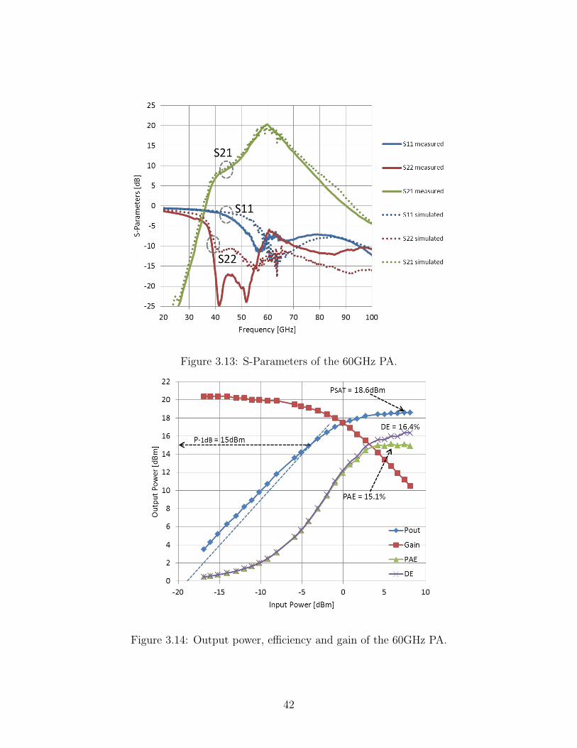
Figure 3.13: S-Parameters of the 60GHz PA.
Figure 3.14: Output power, efficiency and gain of the 60GHz PA.
42

Figure 3.15: 60GHz PA large signal performance across the IEEE 802.15.3c band.
Figure 3.16: Chip micrograph of the 60GHz PA.
43

58 59 60 61 62 63−40
−35
−30
−25
−20
−15
−10
−5
0
Frequency (GHz)
Spe
ctru
m (
dB)
Figure 3.17: PA output spectrum and 802.15.3c spectral mask for Channel 2
60 61 62 63 64 65−40
−35
−30
−25
−20
−15
−10
−5
0
Frequency (GHz)
Spe
ctru
m (
dB)
Figure 3.18: PA output spectrum and 802.15.3c spectral mask for Channel 3
44

−1.5 −1 −0.5 0 0.5 1 1.5−1.5
−1
−0.5
0
0.5
1
1.5Channel 2 (EVM: −17.7dB)
Figure 3.19: Received constellation of the 3.8Gb/s 512 sub-carrier 16-QAM OFDM signal
for Channel 2.
−1.5 −1 −0.5 0 0.5 1 1.5−1.5
−1
−0.5
0
0.5
1
1.5Channel 3 (EVM: −17dB)
Figure 3.20: Received constellation of the 3.8Gb/s 512 sub-carrier 16-QAM OFDM signal
for Channel 3.
45

plotted as a function of average transmitted power in Fig. 3.21 and Fig. 3.22. To achieve-20 dB EVM, the required back-off from 1dB compression point (15 dBm for channel 2 and14.5 dBm for channel 3) is around 7.5 dB. The required back-off reduces to 6dB for -17dBEVM. The PA efficiencies at 6dB backoff and 7.5dB backoff are 2% and 1.5% respectively.
Finally, the above EVM measurement has been performed at different ambient tempera-tures. Heat was applied to the probe station chuck where the silicon die resides. Fig. 3.23 andFig. 3.24 show the measured EVM curves at several different temperature settings. Clearly,both EVM and average output power degrade when temperature increases. The degradationis relatively small from 25C to 50C, and become more significant for temperatures greaterthan 75C. Note that under all the measurement, the transistor gate bias voltage is keptconstant, which means the actual bias current reduces with increasing temperature. Theimpact of temperature on output power can be slightly reduced by using constant currentbiasing or Proportional To Absolute Temperature (PTAT) current biasing.
46
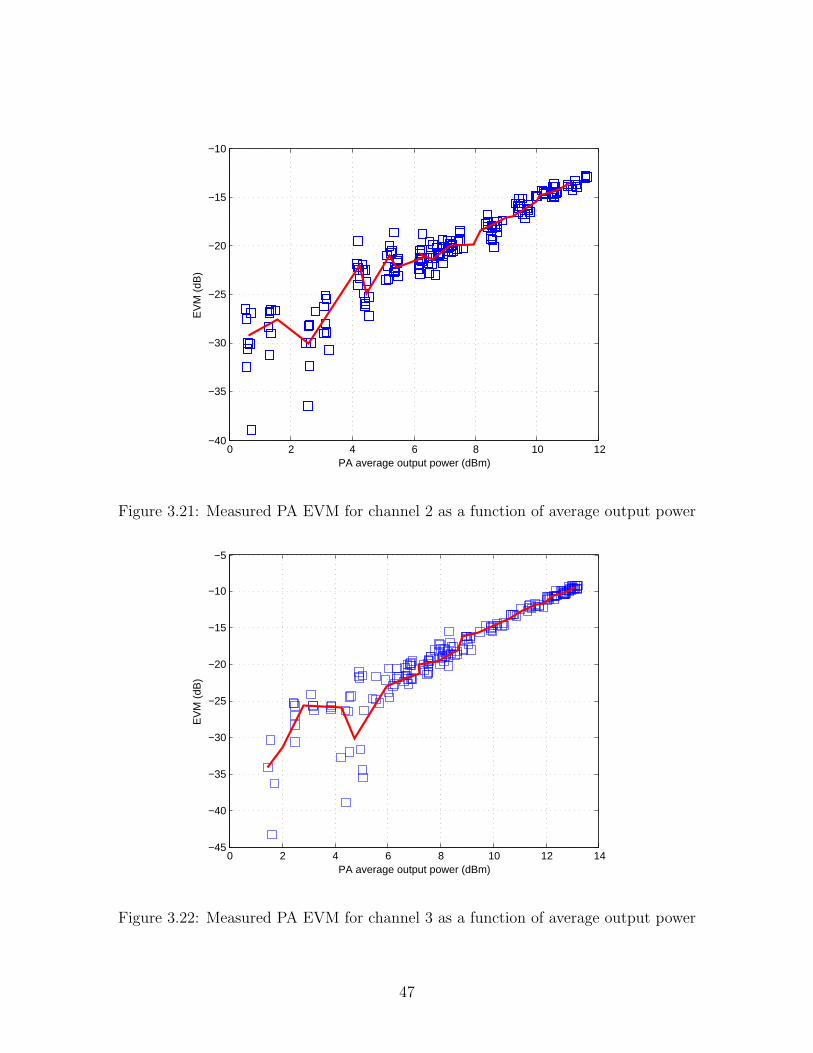
0 2 4 6 8 10 12−40
−35
−30
−25
−20
−15
−10
PA average output power (dBm)
EV
M (
dB)
Figure 3.21: Measured PA EVM for channel 2 as a function of average output power
0 2 4 6 8 10 12 14−45
−40
−35
−30
−25
−20
−15
−10
−5
PA average output power (dBm)
EV
M (
dB)
Figure 3.22: Measured PA EVM for channel 3 as a function of average output power
47

0 2 4 6 8 10 12−40
−35
−30
−25
−20
−15
−10
PA Modulated Output Power (dBm)
EV
M (
dB)
Channel 2
25C
50C
75C
100C
125C
Figure 3.23: Measured PA EVM characteristic for channel 2 at different ambient tempera-
tures.
0 2 4 6 8 10−35
−30
−25
−20
−15
PA Modulated Output Power (dBm)
EV
M (
dB)
Channel 3
25C
50C
75C
100C
Figure 3.24: Measured PA EVM characteristic for channel 3 at different ambient tempera-
tures.
48
Chapter 4
Beamforming Transmitter
As discussed in the previous chapter, the obtainable PA output power drops with fre-quency due to low supply voltage and passive loss. Even with power combining, the maximumoutput power is still limited. With DAT combiners, the achievable output power at 60GHzis around 28dBm for a power gain of 3dB. An alternative to increase the transmitter EIRP isto increase the antenna gain. Increased antenna gain means that the radiated energy is moreconcentrated towards one particular direction, and longer communication distance can beobtained. However, larger antenna gain reduces the signal strength in other directions, andto redirect the energy, the antenna must be physically rotated. Such mechanical movementis very inconvenient and costly. Beamforming transmitters realize an electrically steerableantenna beam by adjusting the electrical signal properties of each antenna element. Beam-forming becomes especially attractive in CMOS since the digital computation and controlcome at an extremely low cost. This chapter discusses the concepts and challenges of CMOSbeamforming, as well as a design example of a low power four element transceiver array.
4.1 Antenna Basics
To fully understand beamforming, the definition of various antenna parameters must beexplained. The most important parameters that characterize an antenna include radiationpattern, gain, efficiency and polarization.
The antenna radiation pattern is defined as a graphical representation of the radiationproperties as a function of space coordinates [19]. Radiation properties include electro-magnetic field strength, power density and directivity etc. The radiation pattern can beconstructed by plotting the received electric field magnitude at a constant radius as a func-tion of angle. Such a pattern is called an amplitude field pattern. Similarly, a plot of receivedpower density is called a power pattern. Fig. 4.1 shows an example antenna radiation pat-
49
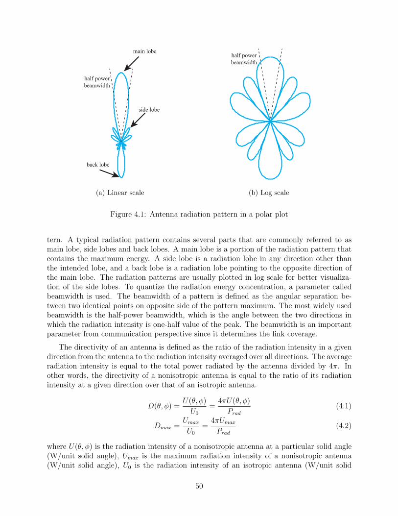
main lobe
side lobe
back lobe
half power
beamwidth
(a) Linear scale
half power
beamwidth
(b) Log scale
Figure 4.1: Antenna radiation pattern in a polar plot
tern. A typical radiation pattern contains several parts that are commonly referred to asmain lobe, side lobes and back lobes. A main lobe is a portion of the radiation pattern thatcontains the maximum energy. A side lobe is a radiation lobe in any direction other thanthe intended lobe, and a back lobe is a radiation lobe pointing to the opposite direction ofthe main lobe. The radiation patterns are usually plotted in log scale for better visualiza-tion of the side lobes. To quantize the radiation energy concentration, a parameter calledbeamwidth is used. The beamwidth of a pattern is defined as the angular separation be-tween two identical points on opposite side of the pattern maximum. The most widely usedbeamwidth is the half-power beamwidth, which is the angle between the two directions inwhich the radiation intensity is one-half value of the peak. The beamwidth is an importantparameter from communication perspective since it determines the link coverage.
The directivity of an antenna is defined as the ratio of the radiation intensity in a givendirection from the antenna to the radiation intensity averaged over all directions. The averageradiation intensity is equal to the total power radiated by the antenna divided by 4π. Inother words, the directivity of a nonisotropic antenna is equal to the ratio of its radiationintensity at a given direction over that of an isotropic antenna.
D(θ, φ) =U(θ, φ)
U0
=4πU(θ, φ)
Prad
(4.1)
Dmax =Umax
U0
=4πUmax
Prad
(4.2)
where U(θ, φ) is the radiation intensity of a nonisotropic antenna at a particular solid angle(W/unit solid angle), Umax is the maximum radiation intensity of a nonisotropic antenna(W/unit solid angle), U0 is the radiation intensity of an isotropic antenna (W/unit solid
50

angle), and Prad is total radiated power (W). Directivity informs how well an antenna canconcentrate energy around a particular spatial direction. Maximum directivity is alwaysgreater than or equal to unity, and the directivity of an isotropic antenna is always unity.Designing antennas usually involves a tradeoff between beamwidth and directivity since thebeamwidth decreases as directivity increases. In reality, an antenna only radiates a portionof the power that it absorbs while the rest of the power is dissipated internally. The internallosses of an antenna include the conduction loss and the dielectric loss. The radiationefficiency is defined as the ratio of the total radiated power to the total absorbed power,
ηrad =Prad
Pin
(4.3)
Taking into account of the radiation efficiency, the antenna gain can be defined,
G(θ, φ) = ηradD(θ, φ) (4.4)
Substitute Eq. 4.1 into Eq. 4.4,
G(θ, φ) =Prad
Pin
4πU(θ, φ)
Prad
(4.5)
=4πU(θ, φ)
Pin
(4.6)
In other words, the gain of an antenna is the ratio of the radiation intensity in a givendirection to the radiation intensity that would be obtained if the power accepted by theantenna were radiated isotropically.
Finally, the polarization of an antenna describes the time-varying orientation of the elec-tric field vector radiated by the antenna. The trace formed by the electric field vector can bea line, a circle or an ellipse, and they correspond to linear polarization, circular polarizationand elliptical polarization respectively. The radiated signal from the transmitter antennacan be completely received only if the receiver antenna has the exactly same polarization.Otherwise, energy is lost due to polarization mismatch. In practice, it’s almost impossible toavoid polarization mismatch since any reflection results in a change in the wave polarization.
Besides the above essential parameters, there are also several other parameters that needto be considered, such as input impedance and bandwidth. The required input impedanceof the antenna is usually 50Ω in order to match the feed line characteristic impedance1. Incases where the antenna is attached very closely to the transmitter or receiver, the inputimpedance can be co-designed with the PA or LNA, and doesn’t necessarily have to be 50Ω.The choice of the impedance should be such that maximizing the PA efficiency or minimizingthe LNA noise figure. The antenna bandwidth is usually set by the system data rate. Higherdate rates usually require larger antenna bandwidth. For example, the WiGig standard hasfour channels from 58.32GHz to 64.8GHz with 2.16GHz channel bandwidth. As a result, theantenna needs to preserve a bandwidth greater than 8GHz.
150Ω impedance also easies the antenna stand-alone characterization since most RF instruments use 50Ωports.
51

4.2 Beamforming through Antenna Array
In high directivity antenna systems, beam steering is essential to cover larger communi-cation angles. Electrical beam steering can be realized by an antenna array with individualcontrol on the signal transmitted or received in each antenna element. Consider a N-elementantenna array shown in Fig. 4.2. To steer the beam θ angle away from the center, the signalsthat excite the antenna element must be progressively delayed such that they add construc-tively in the desired transmission direction. Suppose the signal inside the nth element isdelayed by (n − 1)τ . Due to the antenna spacing d, signals emitted by different antennaelements have different delays to the wavefront. The free space delay difference between thenth antenna and the last (N th) antenna is,
tn =(N − n)d sin θ
c= (N − n)t0 (4.7)
t0 =d sin θ
c(4.8)
The E-field vector contributed by the nth antenna at the wavefront is,
En = ejω0[t−tn−(n−1)τ ] (4.9)
= ejω0[t−(N−n)t0−(n−1)τ ] (4.10)
= ejω0[t−(N−1)t0]ejω0[(n−1)(t0−τ)] (4.11)
Summing the E-field vectors of all N antenna,
Earray =N∑
n=1
En (4.12)
= ejω0[t−(N−1)t0]
N∑
n=1
ejω0[(n−1)(t0−τ)] (4.13)
= ejω0[t−(N−1)t0]
N−1∑
n=0
ejω0[n(t0−τ)] (4.14)
= ejω0[t−(N−1)t0]ejω0(N−1)(t0−τ)
2sin[1
2Nω0(t0 − τ)]
sin[12ω0(t0 − τ)]
(4.15)
The magnitude of the summed E-field vector is,
|Earray| =∣
∣
∣
∣
sin[12Nω0(t0 − τ)]
sin[12ω0(t0 − τ)]
∣
∣
∣
∣
(4.16)
The summed E-field magnitude can be maximized at spatial angle θ by setting τ = t0,
τopt = t0 =d sin θ
c(4.17)
52

0 τ 2τ 3τ (N-1)τ
θ
d
(N-1
)d si
nθ
Ant1 Ant2 Ant3 Ant4 AntN
Figure 4.2: N-element timed array.
Under this condition, the maximum summed E-field magnitude is N times larger than the E-field magnitude of a single antenna. Since the power is proportional to the E-field magnitudesquare, the maximum radiation intensity is N2 times larger than that of a single antenna.In other words, EIRP of an N-element beamforming array is N2 times larger than the EIRPof a single antenna. The E-field magnitude can be expressed as a function of spatial angle θfor a fixed delay τ ,
|Earray(θ)| =∣
∣
∣
∣
∣
sin[12Nω0(
d sin θc
− τ)]
sin[12ω0(
d sin θc
− τ)]
∣
∣
∣
∣
∣
(4.18)
The peak directivity of an N-element array can be calculated,
Darray,max =Umax
U0
=E2
max
E20
=1NN2
1= N (4.19)
The factor 1N
in the numerator comes from the fact that each element gets one-Nth of theinput power. As a result, the peak directivity of an N-element antenna array is N timeslarger than that of a single antenna.
Programmable time delays are usually difficult to implement in a compact fashion. In-stead, most beamforming arrays are actually phased arrays. For narrow band signals, a timedelay can be approximated by a phase shift. Fig. 4.3 shows a N-element phased array. In aphased array, the signals that excite the antennas are progressively phase shifted: the signal
53

0 ø 2ø 3ø (N-1)ø
θ
d
(N-1
)d si
nθ
Ant1 Ant2 Ant3 Ant4 AntN
Figure 4.3: N-element phased array.
inside the nth element is phase shifted by (n − 1)φ. The E-field vector contributed by thenth antenna is,
En = ejω0[t−tn−(n−1) φ
ω0]
(4.20)
= ejω0[t−(N−1)t0]ejω0[(n−1)(t0−
φ
ω0)]
(4.21)
The sum of all the E-field vectors is,
Earray = ejω0[t−(N−1)t0]ejω0
(N−1)(t0−φω0
)
2sin[1
2N(ω0t0 − φ)]
sin[12(ω0t0 − φ)]
(4.22)
The magnitude of the summed E-field vector is,
|Earray| =∣
∣
∣
∣
sin[12N(ω0t0 − φ)]
sin[12(ω0t0 − φ)]
∣
∣
∣
∣
(4.23)
Similar to Eq. 4.17, the summed E-field magnitude can be maximized at spatial angle θ bysetting ω0t0 = φ,
φopt = ωt0 =ω0d sin θ
c(4.24)
Finally the E-field radiation pattern can be found for a fixed phase shift φ,
|Earray(θ)| =∣
∣
∣
∣
∣
sin[12N(ω0
d sin θc
− φ)]
sin[12(ω0
d sin θc
− φ)]
∣
∣
∣
∣
∣
(4.25)
54

Fig. 4.4 plots the E-field magnitude pattern for an 8 element array and a 32 element array,with φ set to direct the beam at different angles: −30, 0 and 30. Apparently larger arrayshave larger directivity and therefore generate shaper beams.
For the same number of elements, the antenna beam pattern is also affected by theelement spacing. Fig. 4.4 assumes half wavelength spacing, which is the maximum limit toavoid large undesired lobes. To illustrate this point, Fig. 4.5 shows the E-field pattern for an8-element array with different antenna spacing. When the spacing exceeds half wavelength,there are multiple side lobes with the same magnitude as the main lobe. These side lobesare called grating lobes. Grating lobes are generally undesired since they steer energy intounwanted direction in a transmitter while pick up interference from other angles in a receiver.As evident in Fig. 4.5, larger antenna spacings result in larger numbers of grating lobes. Thenumber of grating lobes is roughly equal to the ratio of the spacing to the half wavelength.
4.3 Phased Array Architectures
There are multiple radio architectures for implementing a phased array, depending onwhere the phase shift occurs on the signal chain. In a direct conversion transmitter, the phaseof the signal can be adjusted at either the RF domain, LO domain, analog baseband domainor digital baseband domain. They correspond to four different phased array architectures,as illustrated in Fig. 4.6. Each architecture has its own advantages and disadvantages,and the optimal architecture is usually application specific, taking into account of variousconsiderations such as frequency, area, power, interference and robustness.
4.3.1 RF Phase Shifting
Shown in Fig. 4.6a, RF phase shifting architecture adjusts the relative phases of differ-ent antenna elements in the RF signal domain. Traditionally, the biggest advantage of thisarchitecture is that it requires the least number of circuit components, and therefore poten-tially the lowest cost and power. In cases of discrete implementation, due to limited routingflexibility and cost of discrete components, RF phase shifting architecture is the most widelyused architecture. Since only one mixer is used, there’s no need to distribute the LO signaland therefore the noise coupling can be minimized on the LO. In the case of a receiver,another advantage is the relaxed mixer linearity requirement. This is because the signalsare combined in the RF domain before entering the mixer, as a result, interference comingfrom the null direction of the beam will be canceled out during the signal summation, aphenomenon called spatial filtering.
However, phase shifters are usually difficult to implement at high frequencies, especiallyat mm-wave range. Most mm-wave phase shifters are built from variable passive componentsand are therefore lossy [20]. In addition, the phase shifter loss is not constant over differentphase settings, thus requiring an amplifier to compensate the gain variation [21, 22]. In
55

−80 −60 −40 −20 0 20 40 60 800
1
2
3
4
5
6
7
8
Spatial Angle (degrees)
E−
field
mag
nitu
de
(a) 8-element array
−80 −60 −40 −20 0 20 40 60 800
5
10
15
20
25
30
35
Spatial Angle (degrees)
E−
field
mag
nitu
de
(b) 32-element array
Figure 4.4: Phased array E-field magnitude patterns
56

−80 −60 −40 −20 0 20 40 60 800
1
2
3
4
5
6
7
8
Spatial Angle (degrees)
E−
field
mag
nitu
de
lambda/2
2*lambda
(a) Half wavelength spacing and two wavelengths spacing
−80 −60 −40 −20 0 20 40 60 800
1
2
3
4
5
6
7
8
Spatial Angle (degrees)
E−
field
mag
nitu
de
lambda/2
4*lambda
(b) Half wavelength spacing and four wavelengths spacing
Figure 4.5: Phased array E-field magnitude patterns with various element spacings
57

addition, the phase shift must maintain the required signal bandwidth as well as linearitysince it resides in the signal path.
4.3.2 LO Phase Shifting
Shown in Fig. 4.6b, LO phase shifting architecture adjusts the relative phases of differentantenna element in the LO signal domain. Unlike RF phase shifting architecture, the phaseshift function is not implemented in the main signal path, but instead on a constant envelopeCW signal. As a result, there’s no bandwidth or linearity requirement on the phase shifter.The LO phase shifting architecture requires more circuit blocks, mainly additional mixers,one for each element. As a result, it seems like such architecture will inevitably incurlarger power consumption. However, this is not case when the mixer sizing is down scaledaccordingly, since each mixer needs to drive only one PA in this architecture whereas themixer in the RF phase-shifting architecture needs to drive all the PAs unless RF drivers areadded.
Similar to RF phase shifting, the main disadvantage of the LO phase shifting architectureis that it requires high frequency phase shifters. In addition, in the case of a receiver, sincethe signals are combined after down conversion, spatial filtering doesn’t occur before themixer. Therefore, it imposes more stringent requirements on the mixer linearity to handlelarge signal interferences.
4.3.3 Analog Baseband Phase Shifting
Shown in Fig. 4.6c, analog baseband (BB) phase shifting architecture adjusts the relativephases of different antenna elements in the analog baseband domain. The main advantage ofthis architecture is that it doesn’t need a high frequency phase shifter. Phase shifting at lowfrequency can be realized with higher resolution, lower power and smaller footprint. Base-band phase shifters are usually implemented using active devices based on I/Q interpolationprinciples. Unlike passive phase shifters, active phase shifters have very small gain variationacross different phase states. Typical analog baseband phase shifters have resolutions higherthan 5 bits with gain variation less than 1dB [23, 24]. In the case of a receiver, since thephase shifter loss is eliminated in the RF domain, the noise figure of this architecture istypically smaller than that of a RF phase shifting architecture with the same signal chainpower.
Similar to the LO phase shifting architecture, since the LO signal needs to be distributedto the local elements, it’s more sensitive to noise. Special care has to be taken to isolatethe LO distribution path from noisy circuitry such as the digital signals. Besides, spatialfiltering occurs in the analog baseband domain, therefore requiring better mixer linearity.
58

DSP
PAø
DAC
LO
PAø
PAø
PAø
(a) RF Phase Shifting
DSP
PA
ø
DAC
LO
PA
ø
PA
ø
PA
ø
(b) LO Phase Shifting
DSP
PAø
DAC
PAø
PAø
PAø
LO
(c) Analog Baseband Phase Shifting
DSP
PAøDAC
PAø
PAø
PAø
LO
DAC
DAC
DAC
(d) Digital Baseband Phase Shifting
Figure 4.6: Phased array architecutres (Transmitter)
59
4.3.4 Digital Baseband Phase Shifting
The final architecture is the digital baseband phase shifting architecture in which phaseshifting function occurs in the digital domain, as shown in Fig. 4.6d. This architecture pro-vides the greatest flexibility since baseband DSP allows complex beamforming algorithms tobe implemented with high accuracy. It also enables spatial multiplexing using Multiple-InputMultiple-Output (MIMO) for higher data rates, which is widely used in 802.11 standards.
However, this architecture suffers from several major disadvantages. First, since thebeamforming is implemented in the digital domain, a high resolution DAC/ADC is needed.This is especially unattractive, since most mm-wave radios have data rates in the rangeof Gb/s and therefore requires GS/s DAC/ADCs. Such high speed data converters areextremely power hungry at high resolution [25]. Even state-of-the-art time interleaved Suc-cessive Approximation Register (SAR) ADC has an energy efficiency of 50fJ/conv-step [26],much higher than MS/s range ADCs used for Wi-Fi where energy efficiency is in the order of10fJ/conv-step. Second, digital baseband phase shifting architecture requires N copies of theentire radio front-end, which increases power and silicon area. Finally the spatial interfer-ence signal exists throughout the entire receiver chain, as a result, the linearity requirementextends to the entire analog baseband chain.
4.4 Architecture Power Comparison
Besides the aforementioned performance tradeoffs among different architectures, the mostcritical factor to consider when choosing the most appropriate architecture is the overallpower consumption, which depends on a number of factors such as number of elements, fre-quency and process. A simplified model is used here to predict the overall power consumptionof different architectures.
The analysis starts with a single-element transmitter which consists of a PA, a mixer anda VCO, as shown in Fig. 4.7. The PA delivers an output power of Po,PA and needs a inputdrive power of Pi,PA from the mixer. The VCO drives the mixer with an LO power of PLO.The power consumption of this transmitter is,
PsingleTX = PPA + Pmix + PV CO (4.26)
=Po,PA
ηPA
+Pi,PA
ηmix
+ PV CO (4.27)
where ηPA and ηmix are the drain efficiencies of the PA and the mixer respectively. The choiceof Pi,PA is important for minimizing the overall power consumption. Since mixers generallyhave lower drain efficiency than amplifiers due to reduced voltage headroom and increasedparasitic capacitances, Pi,PA should be minimized as much as possible, which means the PAneeds to have multiple stages. On the other hand, due to the finite Q of on-chip inductors,the realizable parallel impedance of an inductor is bounded. This means the mixer powerconsumption cannot be indefinitely down-scaled with Pi,PA. As a result, an optimal Pi,PA
60

PA
Pi,PA Po,PAPLO
Figure 4.7: Single element transmitter.
PAø
PAøLOdr
(a) Implementation A
PAø RFdr
PAø RFdr
(b) Implementation B
Figure 4.8: RF phase shifting.
PA
ø LOdr
PA
ø LOdr
Figure 4.9: LO phase shifting.
PAø
LOdr
PAø
LOdr
Figure 4.10: Analog baseband phase shifting.
61

and mixer size exist for a given technology and operating frequency. It’s assumed that thePi,PA used in the equation represents such an optimal value.
The following subsections derive the power consumption of the RF blocks for RF, LOand ABB phase shifting architectures. The DBB phase shifting architecture has the sameRF power consumption as the ABB phase shifting architecture and therefore is not repeatedin the derivation.
4.4.1 RF Phase Shifting
There are two ways of extending a single-element transmitter into a multi-element RFphase shifting transmitter, as shown in Fig. 4.8. In implementation A, the mixer is up-sizedto provide larger output power in order to drive multiple elements. In implementation B,the mixer is kept unchanged, instead drivers are added in each element to compensate thepower splitting loss and to drive the PA. The RF phase shifters are assumed passive devicesand have a power gain of GPS (GPS < 1).
In implementation A, the upsized mixer needs to deliver a total output power ofNPi,PA/GPS. As a result, the mixer power consumption is,
Pmix =Po,mix
ηmix
(4.28)
= NPi,PA
GPSηmix
(4.29)
where N is the number of array elements. Since the mixer is upsized, LO drivers are neededafter the VCO to provide additional LO power to drive the mixer, the power of the LOdrivers can be found according the output power and gain requirement,
PLOdr =PLO
NGPS
ηamp,non
(4.30)
where ηamp,non represents the drain efficiency of RF (or LO) amplifiers. Note the subnotenon indicates that linearity is not required in this amplifier since it’s in the LO path, asa result, ηamp,non can be higher than ηamp,lin. Given the relation between PAE and drainefficiency defined in Eq. 2.17, Eq. 4.30 can be re-arranged to,
PLOdr =PLON
GPSPAEamp,non
GLOdr − 1
GLOdr
(4.31)
=PLO
PAEamp,non
N −GPS
GPS
(4.32)
=Pi,PA
PAEamp,non
N −GPS
GPSGmix
(4.33)
where,
GLOdr =N
GPS
(4.34)
62
and Gmix is the power gain of the mixer. Note that PAE is used instead of drain efficiencybecause it’s independent of the number of amplifier stages as shown in Eq. 2.21. Thus, thetotal power consumption of implementation A is,
PTX,RFPS−A = Pmix + PLOdr +NPPA (4.35)
=Pi,PA
ηmix
N
GPS
+ (N −GPS)Pi,PA
PAEamp,non
1
GmixGPS
+NPo,PA
ηPA
(4.36)
=Pi,PA
ηmix
+ (N −GPS)Pi,PA
ηmixGPS
+ (N −GPS)Pi,PA
PAEamp,non
1
GmixGPS
+NPo,PA
ηPA
(4.37)
In implementation B, the mixer power consumption is kept unchanged, and the additionalpower comes from the RF drivers in each element. The power consumption of each drivercan be found based on the output power and the gain requirement,
PRFdr =Pi,PA
ηamp,lin
(4.38)
=Pi,PA
PAEamp,lin
GRFdr − 1
GRFdr
(4.39)
=Pi,PA
PAEamp,lin
N −GPS
N(4.40)
where
GRFdr =N
GPS
(4.41)
Therefore the total power consumption of implementation B is,
PTX,RFPS−B = Pmix +NPRFdr +NPPA (4.42)
=Pi,PA
ηmix
+ (N −GPS)Pi,PA
PAEamp,lin
+NPo,PA
ηPA
(4.43)
Comparing Eq. 4.37 and Eq. 4.43, it’s not difficult to conclude that implementation B ismore power efficiency, since GPSηmix is most likely to be smaller than PAEamp,lin. This isbecause the efficiency of a mixer is usually smaller than that of an amplifier and the gainof the phase shifter is usually much smaller than one. Besides, Eq. 4.37 has an extra thirdterm which does not exist in Eq. 4.43. The intuition behind the finding is that more efficientblocks such as amplifiers should be used to provide driving capability in order to lower theoverall power consumption.
Note that although passive RF phase shifters are assumed for calculation, the resultsalso apply when active phase shifters are used. Active phase shifters are typically made ofweighted I/Q summation and can always be separated into the gain stage and the summationstage. The gain stage can be lumped into RF drivers while the summation stage is passiveand lossy. The I/Q summation typically introduces 3dB insertion loss.
63

4.4.2 LO Phase Shifting
In the LO phase shifting architecture, as shown in Fig. 4.9, the mixer and PA in eachelement remains unchanged while LO drivers are required to compensate for the LO signaldistribution and phase shifter loss. The power consumption of each LO driver is,
PLOdr =PLO
ηamp,non
(4.44)
=PLO
PAEamp,non
GLOdr − 1
GLOdr
(4.45)
=PLO
PAEamp,non
N −GPS
N(4.46)
where
GLOdr =N
GPS
(4.47)
The total power consumption of this architecture is,
PTX,LOPS = NPmix +NPLOdr +NPPA (4.48)
= NPi,PA
ηmix
+ (N −GPS)PLO
PAEamp,non
+NPo,PA
ηPA
(4.49)
=Pi,PA
ηmix
+ (N − 1)Pi,PA
ηmix
+ (N −GPS)Pi,PA
GmixPAEamp,non
+NPo,PA
ηPA
(4.50)
=Pi,PA
ηmix
+ (N − 1)Pi,PA
PAEmix
Gmix − 1
Gmix
+ (N −GPS)Pi,PA
GmixPAEamp,non
+NPo,PA
ηPA
(4.51)
=Pi,PA
ηmix
+ (N − 1)Pi,PA
PAEamp,non
1
Gmix
[N −GPS
N − 1+
PAEamp,non
PAEmix
(Gmix − 1)]
+NPo,PA
ηPA
(4.52)
where PAEmix is the LO to RF power added efficiency of the mixer.
It’s relative hard to conclude whether LO phase shifting is better than RF phase shiftingby directly comparing Eq. 4.52 to Eq. 4.43, however, it will be shown that LO phase shiftingarchitecture is almost always inferior to Anlog BB phase shifting architecture.
4.4.3 Analog Baseband Phase Shifting
The transmitter block diagram for analog baseband phase shifting is very similar to thatof LO phase shifting, as shown in Fig. 4.10, with the only difference being that the LO phaseshifter is now moved to the baseband path. As a result, it’s not necessary to repeat the
64

derivation again. Instead, the total power consumption can be readily obtained by settingthe phase shifter gain to unity GPS = 1,
PTX,ABBPS = NPmix +NPLOdr +NPPA (4.53)
= NPi,PA
ηmix
+ (N − 1)PLO
PAEamp,non
+NPo,PA
ηPA
(4.54)
=Pi,PA
ηmix
+ (N − 1)Pi,PA
ηmix
+ (N − 1)Pi,PA
GmixPAEamp,non
+NPo,PA
ηPA
(4.55)
=Pi,PA
ηmix
+ (N − 1)Pi,PA
PAEmix
Gmix − 1
Gmix
+ (N − 1)Pi,PA
GmixPAEamp,non
+NPo,PA
ηPA
(4.56)
=Pi,PA
ηmix
+ (N − 1)Pi,PA
PAEamp,non
1
Gmix
[1 +PAEamp,non
PAEmix
(Gmix − 1)] +NPo,PA
ηPA
(4.57)
Comparing Eq. 4.57 to Eq. 4.52, it can be seen that the RF power consumption of analogbaseband phase shifting architecture is always smaller than that of the LO phase shiftingarchitecture due to absence of phase shifter loss. Note that the baseband phase shifter poweris not included in the comparison and such omission is generally acceptable since basebandcircuit blocks typically consume much lower power than RF blocks.
Comparing analog baseband phase shifting architecture and RF phase shifting architec-ture is less straightforward. Note that the first and third terms in Eq. 4.43 to Eq. 4.57 areidentical, therefore only the second term needs to be compared. In fact the second termrepresents the overhead RF power when scaling the transmitter from single element to Nelements,
∆PTX,RFPS−B = (N −GPS)Pi,PA
PAEamp,lin
(4.58)
∆PTX,ABBPS = (N − 1)Pi,PA
PAEamp,non
1
Gmix
[1 +PAEamp,non
PAEmix
(Gmix − 1)] (4.59)
When the mixer gain Gmix is much greater than unity, Eq. 4.59 can be simplified to,
∆PTX,ABBPS = (N − 1)Pi,PA
PAEmix
(4.60)
Since the amplifier PAE is typically larger than the mixer PAE, it’s almost certain that forreasonably large arrays, the RF phase shifting is more power efficient. This means for lowfrequency applications, the RF phase shifting architecture is the best candidate. However,if the ratio of PAEamp,lin to PAEmix is less than two, it’s possible that the analog basebandphase shifting architecture is more efficient for small arrays.
65

4.4.4 Generalized Comparison
To provide more insights on the power comparison, the overhead power of the threearchitectures is plotted for different array sizes based on different Gmix and
PAEamp,lin
PAEmixvalues.
With a mixer gain of 2 (Gmix = 2), if an amplifier is three times more efficient than a mixer
(PAEamp,lin
PAEmix= 3), the RF phase shifting is always better than baseband phase shifting, no
matter how many elements the array has, as shown in Fig. 4.11. If an amplifier is two timesmore efficient than a mixer, the baseband phase shifting architecture is better for arraysizes smaller than 5, as shown in Fig. 4.12. If an amplifier is only 1.75 times more efficientthan a mixer, the baseband phase shifting architecture remains better for array sizes up to8. As a result, the smaller
PAEamp,lin
PAEmixis, the more efficient analog baseband phase shifting
architecture is. On the other hand, the larger the mixer gain is, the less attractive theanalog baseband phase shifting architecture becomes, as evident when comparing Fig. 4.13and Fig. 4.14. When the mixer gain is doubled, the crossover point for the RF phase shiftingand baseband phase shifting drops from 8 to 3. In short, the slope of the overhead power foranalog baseband phase shifting architecture increases with mixer gain Gmix as well as theefficiency ratio of amplifiers and mixer
PAEamp,lin
PAEmix. For large array sizes, RF phase shifting is
always more power efficient than baseband phase shifting since slope of overhead power foranalog baseband phase shifting is always larger than that of RF phase shifting.
4.5 Phase Shifters
4.5.1 Resolution
The minimum phase shifter resolution is determined by the directivity of the array.Fig. 4.15 to Fig. 4.18 show the obtainable array gain as a function of the beamformingangles with different phase shifter resolutions for different array sizes. At each beamformingangle, the phase setting of each element is chosen such that the total array gain is maximizedat that angle. It can be seen that 2-bit phase shifter resolution is already sufficient to obtainan array gain within 1dB range of the theoretical maximum. 3-bit resolution closes thegap to less than 0.3dB. Further increasing the resolution has diminishing returns in termsof array gain improvement. As a result, 4-bit might be enough for any array size fromthe perspective of array gain. On the other hand, phase shifter resolution also affects thesidelobe level and the peak-to-null ratio. Fig. 4.19 and Fig. 4.20 show the maximum sidelobelevel and minimum peak-to-null ratio as a function of beamforming angles for a 4-elementarray. Again, the phase setting for each element is chosen to optimize the array gain ateach beamforming angle. Clearly, higher phase shifter resolution reduces the maximumsidelobe and increases the minimum peak-to-null ratio, which is highly desired to minimizeinterference and multi-path fading. These improvements are more significant than array gainimprovement at higher phase shifter resolutions.
66

2 3 4 5 6 7 80
20
40
60
80
100
120
140
Number of Elements
Overh
ead P
ow
er
(mW
)
RFPS
LOPS
BBPS
Figure 4.11: Overhead power (Gmix = 2,PAEamp,lin
PAEmix= 3,
PAEamp,lin
PAEamp,non= 2,GPS = 1/8)
2 3 4 5 6 7 810
20
30
40
50
60
70
80
90
Number of Elements
Overh
ead P
ow
er
(mW
)
RFPS
LOPS
BBPS
Figure 4.12: Overhead power (Gmix = 2,PAEamp,lin
PAEmix= 2,
PAEamp,lin
PAEamp,non= 2,GPS = 1/8)
67

2 3 4 5 6 7 810
20
30
40
50
60
70
80
90
Number of Elements
Overh
ead P
ow
er
(mW
)
RFPS
LOPS
BBPS
Figure 4.13: Overhead power (Gmix = 2,PAEamp,lin
PAEmix= 1.75,
PAEamp,lin
PAEamp,non= 2,GPS = 1/8)
2 3 4 5 6 7 80
20
40
60
80
100
120
Number of Elements
Overh
ead P
ow
er
(mW
)
RFPS
LOPS
BBPS
Figure 4.14: Overhead power (Gmix = 4,PAEamp,lin
PAEmix= 1.75,
PAEamp,lin
PAEamp,non= 2,GPS = 1/8)
68

−100 −80 −60 −40 −20 0 20 40 60 80 100
5.4
5.5
5.6
5.7
5.8
5.9
6
6.1
incident angle (degrees)
arr
ay g
ain
(dB
)
2−bit 3−bit 4−bit 5−bit
Figure 4.15: Array gain as a function of beamforming angle (2 elements)
−100 −80 −60 −40 −20 0 20 40 60 80 10011.1
11.2
11.3
11.4
11.5
11.6
11.7
11.8
11.9
12
12.1
incident angle (degrees)
arr
ay g
ain
(dB
)
2−bit 3−bit 4−bit 5−bit
Figure 4.16: Array gain as a function of beamforming angle (4 elements)
69

−100 −80 −60 −40 −20 0 20 40 60 80 10017
17.2
17.4
17.6
17.8
18
18.2
incident angle (degrees)
arr
ay g
ain
(dB
)
2−bit 3−bit 4−bit 5−bit
Figure 4.17: Array gain as a function of beamforming angle (8 elements)
−100 −80 −60 −40 −20 0 20 40 60 80 10023
23.2
23.4
23.6
23.8
24
24.2
incident angle (degrees)
arr
ay g
ain
(dB
)
2−bit 3−bit 4−bit 5−bit
Figure 4.18: Array gain as a function of beamforming angle (16 elements)
70

−100 −80 −60 −40 −20 0 20 40 60 80 100−12
−11
−10
−9
−8
−7
−6
−5
−4
incident angle (degrees)
maxim
um
sid
elo
be (
dB
)
2−bit 3−bit 4−bit 5−bit
Figure 4.19: Maximum sidelode as a function of beamforming angle (4 elements)
−100 −80 −60 −40 −20 0 20 40 60 80 100−55
−50
−45
−40
−35
−30
−25
−20
−15
−10
−5
incident angle (degrees)
min
imum
nul
l−to
−pea
k (d
B)
2−bit 3−bit 4−bit 5−bit
Figure 4.20: Minimum peak-to-null ratio as a function of beamforming angle (4 elements)
71
4.5.2 Implementation
Depending on the frequency, phase shifters can be either passive or active. Passivephase shifters are mainly used in the RF signal domain. In general, passive phase shifterscan be classified into two categories: through type phase shifters and reflective type phaseshifters. Through type phase shifters are essentially tunable LC delay structures, as shownin Fig. 4.21. The insertion time delay and phase shift are,
tD =√
LtotCtot (4.61)
φ = ω√
LtotCtot (4.62)
The simplest way to implement such a phase shifter is to have multiple T-lines with differentlengths (Fig. 4.21a). The input and output are switched between different T-lines for differentphase shift. Obviously such an approach can only have very low resolution or range unlesslarge silicon area is used. A better approach is to synthesize a T-line using variable capacitorsand inductors (Fig. 4.21b). Traditionally, only variable capacitors are used since it can beeasily implemented by varactors or switched capacitors while variable inductors are muchmore difficult to implement. However, this changes the characteristic impedance of theT-line and thus reduces the bandwidth. Besides it also limits the obtainable phase shiftrange. Recently variable inductors were also demonstrated using inductance multiplicationtechniques [27]. Although only 1-bit variable inductor was implemented, it significantlyextended the phase shift range and preserved the wide band characteristic of a T-line.
Reflective type phase shifters exploit the reflection coefficient property of a LC resonancetank. The reflection coefficient of a parallel LC tank has a constant magnitude of unity, but avarying phase depending on the offset from the resonance frequency. By loading a quadraturehybrid with two LC tanks with variable resonance frequency (Fig. 4.22), the signal goingthrough the hybrid will experience variable phase shifts. The phase response of this structureis,
φ ≈ −2 arctan(2Z0
Z0,tank
δω
ω0
) (4.63)
ω0 =1√LC0
(4.64)
Z0,tank =√
L/C0 (4.65)
where C0 and Z0,tank are the nominal capacitance and impedance of the tank, and δω is shiftin tank resonance frequency when the capacitance is varied. Although such a structure canprovide up to 360 total phase shift in theory, the amount of variable capacitance that canbe implemented usually limits the total range. As a result, two or more stages are usuallycascaded to cover 360 [28, 27]. Alternatively, an active stage can be used to provide 180
phase invertion [21]. This active stage can also compensate the gain variation of the passivephase shifter at different phase states.
Active phase shifters are based on I/Q interpolation. By summing differently weightedcosine and sine signals, a new phase can be obtained. The relative phase shift is determined
72

in out
(a) variable T-line lengths
in out
(b) Synthesized T-line with variable LC
Figure 4.21: Through type phase shifters
in
out
λ/4
λ/4
Figure 4.22: Reflection type phase shifter
by the relative weighting assigned to the cos and sin signals,√
A2I + A2
Q cos(ωt+ φ) = AI cos(ωt) + AQ sin(ωt) (4.66)
φ = − arctan(AQ
AI
) (4.67)
The programmable weightings are usually implemented by two Variable Gain Amplifiers(VGAs). Fig. 4.23 shows several different implementations. In the first implementation(Fig. 4.23a), the variable gain function is achieved by programming the current source value,and the quadrant selection is performed by directing current to one of the two Gilbertdifferential pairs. The advantage of this implementation is high current efficiency sinceall the current is utilized. The downside is the varying output common level and thusvarying output voltage swing headroom. In the second implementation (Fig. 4.23b), thevariable gain function is achieved by unequally distribute a total constant current to twoGilbert differential pairs to achieve a variable differential output current. Compared to thefirst implementation, this architecture has constant output common mode but less currentefficiency since the differential output current is only a fraction of the total bias current.In both implementations, the original signal (cosine signal or sine signal) has to drive fourtransistors that form the Gilbert quad to enable quadrant swapping. In contrast, the thirdand fourth implementation places the quadrant selection at the input of the amplifier using
73

Iin
Qin
out
i0+ i1+ ik-1+
ik+ ik-
1x 2x 2k-1x
(a)
Iin
Qin
out
1x 2x 2kx
i0-
i0+
i1-
i1+
ik-
ik+
(b)
Iin+
Qin
out
i0+ i1+ ik-1+
ik+
ik-
1x 2x 2k-1x
Iin-
ik-
ik+
(c)
Iin+
Qin
outi0+
i0-
1x 2kx
Iin-
i0-
i0+
Iin+ik+
ik-
Iin-
ik-
ik+
(d)
Figure 4.23: I/Q interpolating phase shifters
pass gates (Fig. 4.23c and Fig. 4.23d). As a result, the loading to the signal path can bereduced by half. The disadvantage is the added loss of the pass gate switches and additionalnoise.
4.6 Low Power 4-Element Phased Array
While the previous sections describe the fundamentals of phased arrays, this sectionfocuses on the design of a mm-wave phased array. Specifically, the phased array operatesat 60GHz and the goal is to achieve 10Gb/s data rate over 2 meters Line-of-Sight (LOS)distance while maintaining low power consumption. The number of phased array elementsis determined based on the tradeoff of power, efficiency and area. For the same EIRP,less PA power is needed with more transmitter elements. However, this doesn’t mean thetransmitter power can be reduced indefinitely. In fact, overhead power from mixer andLO distribution increases with the number of elements, as a result, there exists an optimalnumber of elements for minimal power consumption. This optimal number depends on a
74

No. of Antennas 4 unitsAntenna Gain -3 dBiArray Gain 12 dBPA Power 0 dBmEIRP 9 dBmDistance 2 metersPath Loss 74 dBRX Input Level -65 dBmRX Noise/Hz -174 dBm/HzRX Bandwidth 5 GHzNoise Level -69 dBmRX Noise Figure 8 dBSNR (one element) 4 dBArray SNR Gain 6 dBRX Array Output SNR 10 dB
Table 4.1: Link budget analysis for a 10Gb/s 60GHz QPSK link over 2 meters
number of factors such as circuit architecture, supply voltage and passive Q-factor. In thisprototype, four elements are chosen [29]. Table. 4.1 shows the link budget analysis for thedesired data rate and distance. A receiver output SNR of 10dB is targeted for obtaining aBER of 10−3 with QPSK modulation.
Based on the preceeding comparison of four different phased array architectures, theanalog baseband phase shifting architecture is chosen for better phase shifter performanceand lower power consumption due to small array size and limited mixer gain (Gmix < 2).The block diagram of the entire transceiver is shown in Fig. 4.24. The transceiver consistsof four TX, four RX, an integrated integer-N frequency synthesizer and a LO distributionnetwork.
Each transmitter element consists of an analog baseband phase shifter, a double-balancedquadrature Gilbert mixer and a ZVS power amplifier (Fig. 4.25). In a relatively low out-put power transmitter, the overall efficiency is no longer determined by the PA since otherblocks in the transmitter chain also contribute a significant portion of the total power con-sumption. Therefore, efficiency optimization is a key design component for every block inthe transmitter chain and this is achieved by various techniques addressed in the followingsubsections.
4.6.1 Phase Rotating Quadrature Mixer
Maximizing the current efficiency of the mixer is critical not only in reducing the mixerpower, but also in maximizing the impedance at the LO ports which reduces the required
75

0˚
90˚
PHASE
ROTATOR
0˚
90˚
PHASE
ROTATOR
PHASE
ROTATOR
0˚
90˚
PHASE
ROTATOR
0˚
90˚
PHASE
ROTATOR
0˚
90˚
PHASE
ROTATOR
0˚
90˚
PHASE
ROTATOR
0˚
90˚
PHASE
ROTATOR
0˚
90˚
I Q
I Q
PRBS
GENERATOR
WILKINSON
HYBRID
CHIP BOUNDARY
PLL
REF CLK
117 MHz
Figure 4.24: Block diagram of the 60GHz four-element phased array transceiver
PR. PA
I′
Q′
G
G
S
2:1
Bias
I
Q
1:1
18/0.06
+ -
LO.I LO.Q
S1 S2 S3 S4 S5 S6 S7 S8
cos sin
10/0.06
S1 = Quad1(1-SI) + Quad3SI
S2 = Quad3(1-SI) + Quad1SI
S3 = Quad4(1-SQ) + Quad2SQ
S4 = Quad2(1-SQ) + Quad4SQ
S5 = Quad1(1-SQ) + Quad3SQ
S6 = Quad3(1-SQ) + Quad1SQ
S7 = Quad2(1-SI) + Quad4SI
S8 = Quad4(1-SI) + Quad2SI
θHS
BB
S1 S2 S1
S7 S8
Figure 4.25: Schematic of the transmitter element
76

LO buffer current swing. Combining the baseband phase shifter and the quadrature mixerinto a single structure is attractive since the bias current can be reused. In such a combinedstructure, the conventional means to achieve phase shift functionality is to current sum theweighted original I and Q signals, as illustrated in Fig. 4.26a. However, this architecturesuffers from relatively low efficiency. To gain insight into the root cause of this poor efficiency,consider the current efficiency of the phase rotator, which is defined as the ratio of theeffective differential output current magnitude to the total DC current,
ηtraditional =
√
I ′2 +Q′2
2(cos θ + sin θ)=
√
I2 +Q2
2(cos θ + sin θ)(4.68)
=1√
2(cos θ + sin θ)(4.69)
where I ′ and Q′ are the phase shifted baseband signals and the final equality is basedon the fact that the original baseband I/Q values are either 1 or -1 for QPSK modulation.Note that the efficiency falls between 50% to 71% depending on phase shift angle θ. Thelow efficiency is further explained by an example shown in Fig. 4.26b. At 45 phase shiftangle with both initial I/Q inputs of 1, one pair of the cos and sin current appears atthe output as common-mode signals to achieve an effective I magnitude of zero. In otherwords, half of the total current is wasted due to the current-mode subtraction inherent in thisstructure. To improve the current efficiency, an improved baseband phase shifter architectureis proposed in Fig. 4.27. In the proposed architecture, only two current sources are usedand instead of carrying cos θ and sin θ weightings, they carry cos(θ + 45) and sin(θ + 45)weightings, representing the magnitude of the phase-rotated I/Q signals. Depending onin which quadrant the final phase-shifted data lands, the cos(θ + 45) weighting shouldrepresent the I ′ signal or the Q′ signal. Since the final data quadrant depends on boththe initial data quadrant and the phase shift angle, eight current distribution switches areused to dynamically distribute the two current sources to the appropriate I/Q output ports.Since the DC current is reduced, the current efficiency can be improved. The new currentefficiency is,
ηproposed =
√
I ′2 +Q′2
2(cos(θ + 45) + sin(θ + 45))(4.70)
=
√
cos2(θ + 45) + sin2(θ + 45)
2(cos(θ + 45) + sin(θ + 45))(4.71)
=1
(cos(θ + 45) + sin(θ + 45))(4.72)
Note that the new efficiency falls between 71% and 100%, a significant improvement com-pared to the conventional approach. Fig. 4.28 plots the efficiency comparison for differentphase shift angles and the new architecture is superior to the conventional one at any anglewith an average improvement of around 40%. The current distribution switches S1-S8 arecontrolled by the baseband input quadrant information (Quad1 to Quad4), which are com-puted from the original I/Q signals, as well as the sign bits of the 7-bit phase shift control,as illustrated in Fig. 4.25. The truth table of the quadrant signals and the correspondence
77

Ip
cos(θ)
InQn
sin(θ)
Qp
I’p I’n
I’=Icos(θ)-Qsin(θ)
Qp
cos(θ)
QnIp
sin(θ)
In
Q’p Q’n
Q’=Qcos(θ)+Isin(θ)
(a)
Ip InQn Qp
I’p I’n
Qp QnIp In
Q’p Q’n
θ=45
I’=0 Q’=√2
√21
√21
√21
√21
Ip=Qp=1
(b)
Figure 4.26: Conventional BB phase shifter architecture
S1 S2 S3 S4 S5 S6 S7 S8
cos(θ+45) sin(θ+45)
I’p I’n Q’p Q’n
θ
θ+45
(I’ Q’)
(I Q)
Figure 4.27: Proposed BB phase shifter architecture
Figure 4.28: Efficiency comparison of the conventional and proposed phase shifters
of the two sign bits and the phase shift region are shown in Table. 4.2 and Table. 4.3. Ateach clock sampling point, only one of the four switches (S1 to S4) connecting the I mixer isturned on while others remain off. The same principle applies to the four switches (S5 to S8)connecting the Q mixer. The current sources are implemented by 5-bit DACs with upper4-bits thermometer encoded. The phase shifted baseband signals are fed into two double-balanced mixers for quadrature modulation. Since the sizes of the Gilbert quad switches setthe driving requirement for the LO buffers, smaller size transistors are preferred to increasethe input impedance and reduce the buffer power. Due to reduced phase shifter current,10µm transistors are used, which present a differential impedance of 1.2kΩ. With a differen-
78

Input (I,Q) Quad1 Quad2 Quad3 Quad4(1,1) 1 0 0 0(-1,1) 0 1 0 0(-1,-1) 0 0 1 0(1,-1) 0 0 0 1
Table 4.2: Truth table of the quadrant signals
SI,SQ (Sign bits of the phase shift setting) Phase shift region in radians(0,0) 0 to π/2(1,0) π/2 to π(1,1) π to 3π/2(0,1) 3π/2 to 2π
Table 4.3: Phase shift region and its corresponding control sign bits
tial input swing of 600mV, the required LO input power is kept below -8dBm. The outputsof the two double-balanced mixers are current combined before feeding to the transformerused for coupling the PA and the mixer. The power consumption of the phase rotating mixervaries between 6-8.75mA depending on the phase shift setting.
4.6.2 ZVS PA
Since QPSK modulation has relatively small PAPR ratio before filtering, this enables theuse of a zero-voltage-switching (ZVS) amplifier for improved efficiency2. Recall in Chapter. 2,it’s shown in Fig. 2.15c that traditional Class-E amplifiers have non-optimal PAE at mm-wave frequency. With harmonic impedance tuning, the extended Class-E/FX amplifiers canpotentially improve the PAE by more than 20%. On the other hand, adding higher orderharmonics beyond the second has diminishing returns in efficiency improvement but resultsin more complexity (and hence additional passive loss) in implementing the on-chip tuningnetwork, and therefore this design limits the harmonic tuning to the second order. In fact, itwill be shown that involving second harmonic tuning is already challenging at this frequencyrange.
Similar to Fig. 2.15c, the drain efficiency, power gain, and PAE of the core PA can beevaluated as a function of the normalized second harmonic reactance (X2) presented to thetransistor (Fig. 4.29). Unlike Fig. 2.15c which is based a generic 65nm process, Fig. 4.29 isbased on ST 65nm GP process with transistor parameters extracted from layout. In addition,a Q-factor of 10 is assumed for an inductor at the fundamental frequency while a Q-factor of
2In cases where the signal is filtered, a linear PA is required to preserve the output spectrum shape. Inother words, filtered QPSK signals have non-negligible PAPR ratio.
79

2
4
6
8
0.4 0.5 0.6 0.7 0.8 0.9 135
45
55
65
X2
Core
Dra
in E
ffic
iency (
%)
Pow
er
Gain
(dB
)
0.4 0.5 0.6 0.7 0.8 0.9 130
35
40
45
Core
PA
E (
%)
X2
Figure 4.29: Predicted PA drain efficiency, power gain and PAE
0 5 10 15 20 25 30 350
1
2
time (ps)
dra
in v
oltage (
V)
0 5 10 15 20 25 30 35
0
20
dra
in c
urr
ent
(mA
)
Figure 4.30: Schematic of the transmitter element
4 is assumed for the second harmonic impedance. Due to decreased FC , decreasing secondharmonic reactance improves the capacitance tolerance of the ZVS topology and allowsa larger switch to be used. As a result, the drain efficiency can be significantly improved.Meanwhile, larger switches lead to larger input power and therefore lower power gain. Finally,the optimal X2 for PAE is around 0.52 at 60GHz, quite close to what’s predicted based ona generic 65nm process.
The tuning network for this design is implemented by a 1-to-1 wide trace broadside
80
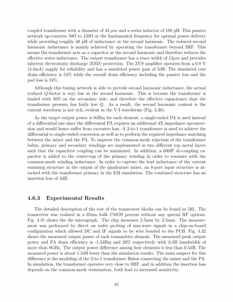
coupled transformer with a diameter of 42 µm and a series inductor of 100 pH. This passivenetwork up-converts 50Ω to 150Ω at the fundamental frequency for optimal power deliverywhile providing roughly 40 pH of inductance at the second harmonic. The reduced secondharmonic inductance is mainly achieved by operating the transformer beyond SRF. Thismeans the transformer acts as a capacitor at the second harmonic and therefore reduces theeffective series inductance. The output transformer has a trace width of 12µm and providesinherent electrostatic discharge (ESD) protection. The ZVS amplifier operates from a 0.8 V(4.4mA) supply for reliability and has a simulated power gain of 5dB. The simulated coredrain efficiency is 54% while the overall drain efficiency including the passive loss and thepad loss is 34%.
Although this tuning network is able to provide second harmonic inductance, the actualrealized Q-factor is very low at the second harmonic. This is because the transformer isloaded with 50Ω on the secondary side, and therefore the effective capacitance that thetransformer presents has fairly low Q. As a result, the second harmonic content is thecurrent waveform is not rich, evident in the V-I waveforms (Fig. 4.30).
As the target output power is 0dBm for each element, a single-ended PA is used insteadof a differential one since the differential PA requires an additional 4X impedance upconver-sion and would hence suffer from excessive loss. A 2-to-1 transformer is used to achieve thedifferential to single-ended conversion as well as to perform the required impedance matchingbetween the mixer and the PA. To improve the common-mode rejection of the transformerbalun, primary and secondary windings are implemented in two different top metal layerssuch that the capacitive coupling can be minimized. In addition, a 600fF de-coupling ca-pacitor is added to the center-tap of the primary winding in order to resonate with thecommon-mode winding inductance. In order to capture the lead inductance of the currentsumming structure at the output of the quadrature mixer, an 8-port input structure is at-tached with the transformer primary in the EM simulation. The combined structure has aninsertion loss of 3dB.
4.6.3 Experimental Results
The detailed description of the rest of the transceiver blocks can be found in [30]. Thetransceiver was realized in a 65nm bulk CMOS process without any special RF options.Fig. 4.31 shows the die micrograph. The chip measures 2.5mm by 3.5mm. The measure-ment was performed by direct on wafer probing of mm-wave signals in a chip-on-boardconfiguration which allowed DC and IF signals to be wire bonded to the PCB. Fig. 4.32shows the measured output power of each transmitter element. The measured peak outputpower and PA drain efficiency is -1.5dBm and 20% respectively with 3-dB bandwidth ofmore than 8GHz. The output power difference among four elements is less than 0.5dB. Themeasured power is about 1.5dB lower than the simulation results. The main suspect for thisdifference is the modeling of the 2-to-1 transformer Balun connecting the mixer and the PA.In simulation, the transformer operates very close to SRF, and in addition the insertion lossdepends on the common-mode termination, both lead to increased sensitivity.
81
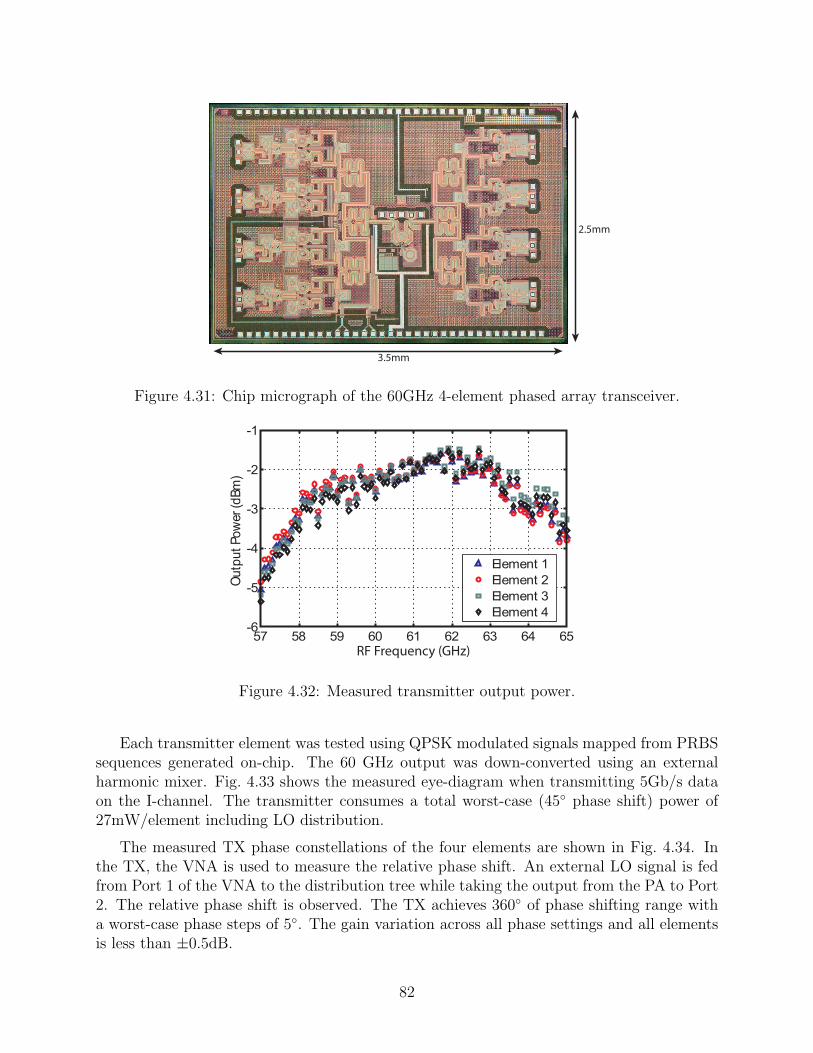
2.5mm
3.5mm
Figure 4.31: Chip micrograph of the 60GHz 4-element phased array transceiver.
57 58 59 60 61 62 63 64 65-6
-5
-4
-3
-2
-1
Outp
ut Pow
er (d
Bm
)
Element 1
Element 2
Element 3
Element 4
RF Frequency (GHz)
Figure 4.32: Measured transmitter output power.
Each transmitter element was tested using QPSK modulated signals mapped from PRBSsequences generated on-chip. The 60 GHz output was down-converted using an externalharmonic mixer. Fig. 4.33 shows the measured eye-diagram when transmitting 5Gb/s dataon the I-channel. The transmitter consumes a total worst-case (45 phase shift) power of27mW/element including LO distribution.
The measured TX phase constellations of the four elements are shown in Fig. 4.34. Inthe TX, the VNA is used to measure the relative phase shift. An external LO signal is fedfrom Port 1 of the VNA to the distribution tree while taking the output from the PA to Port2. The relative phase shift is observed. The TX achieves 360 of phase shifting range witha worst-case phase steps of 5. The gain variation across all phase settings and all elementsis less than ±0.5dB.
82

−1 −0.5 0 0.5 1−0.4
−0.3
−0.2
−0.1
0
0.1
0.2
0.3
0.4
Unit Interval
Norm
aliz
ed A
mplit
ude
Eye Diagram
5Gb/s
Figure 4.33: Measured eye-diagram of the I-channel while transmitting 5Gb/s QPSK data.
The two-element phased array normalized gain is shown in Fig. 4.34a as a function ofrelative phase shift angle. This two-element measurement was performed by using dual GSGprobes and off-chip power combiners which allowed simultaneous probing of both elements.The phase setting of one element was held constant while the phase shift on the other elementwas swept over its entire range. Due to the high phase resolution and low gain mismatch, themeasured peak-to-null ratio on the TX is 40dB. This also confirms that the on-chip isolationbetween elements is sufficient to obtain a good peak-to-null ratio.
Although 4-element beamforming pattern is unavailable due to lack of antenna arrayintegration, a synthesized pattern was constructed using the measured 4 TX element powerand phase characteristics (Fig. 4.34b). The pattern is based on a λ/2 uniformly spaced array.In such an array pattern, the peak gain is not as sensitive as the nulls to the mismatch ingain and phase between elements. Thus, the close matching between ideal and synthesizedarray patterns shown in Fig. 4.34b further confirms the high resolution and accuracy of theproposed transceiver design.
83

0.5
1
1.5
30
210
60
240
90
270
120
300
150
330
180 0
Element 1 Element 2 Element 3 Element 4
Figure 4.34: Measured phase constellations for four TX elements.
0 30 60 90 120 150 180 210 240 270 300 330 360−50
−45
−40
−35
−30
−25
−20
−15
−10
−5
0
Phase (degrees)
Norm
alz
ied G
ain
(dB
)
(a) Two element measured
-90 -75 -60 -45 -30 -15 0 15 30 45 60 75 90-50
-40
-30
-20
-10
0
Phase (degree)
No
rma
lize
d G
ain
(d
B)
synthesized
ideal
(b) Four element synthesized
Figure 4.35: Transmitter beamforming pattern.
84

Chapter 5
Direct Digital-to-RF Transmitter
The previous chapters present the architectures and circuit techniques mainly for im-proving the mm-wave transmitter peak output power/EIRP. However, mm-wave transmit-ters suffer from not only low power handling capability, but also low efficiency, as evidentin Fig. 2.16. This is mainly caused by reduced available power gain and increased deviceparasitic loss. Unlike lower frequency counterparts, mm-wave PAs typically include multipledriver stages to obtain the desired power gain, which leads to a larger difference betweenthe 1dB gain compressed output power (P1dB) and the saturated output power (Psat) dueto simultaneous gain compression from multiple stages. Such discrepancy can be as large as3-4dB [31, 32]. Since the extra power beyond P1dB cannot be utilized in a linear transmitterdue to amplitude distortion, the actual peak efficiency is already significantly reduced1. Tomake matters worse, most digital modulation schemes widely used today have a fairly highPAPR, which demands the transmitter to back-off from its peak linear output power levelP1dB. Since the efficiency of Class-A PAs drops linearly with output power, a 6dB powerback-off reduces the PA efficiency by 75%. As a result, the average efficiency during datatransmission is only a small fraction of the peak efficiency. Various techniques have beenintroduced to enhance the average efficiency, however, challenges remain to adopt them formm-wave transmitters. This chapter presents a direct digital-to-RF conversion architecturethat enables dynamic DC power scaling at very high data rates and thus significantly im-proves the mm-wave transmitter average efficiency. By utilizing a concept called QuadratureSpatial Combining, both I/Q load-pull and insertion loss present in a traditional Cartesiantransmitter can be minimized simultaneously. The rest of this chapter is organized as follows.It first reviews traditional efficiency enhancing architectures that are widely used at lower fre-quencies and discusses challenges for high frequency adoption. Section 2 introduces the directdigital-to-RF architecture and discusses the practical implementation at mm-wave frequencydomain. Section 3 presents the Quadrature Spatial Combining concept and its implicationson the PA performance and beamforming. The circuit implementation of an eight-element
1The efficiency numbers in Fig. 2.16 are mostly those at Psat for mm-wave PAs. Efficiencies at P1dB areusually half.
85

(4I+4Q) 60GHz digital-to-RF conversion beamforming transmitter is presented in section 4,followed by experimental results in section 5. Finally, digital calibration and pre-distortiontechniques are discussed in section 6.
5.1 Traditional Efficiency Enhancing Architectures
The main reason behind the low average efficiency of Class-A PAs is that the DC powerconsumption remains constant and independent of the instantaneous signal amplitude. Inother words, the larger the PAPR is, the lower the average efficiency becomes. A number oftransmitter architectures have been proposed to improve the average efficiency by enablingdynamic DC power scaling through various ways. Three most popular architectures areenvelope tracking, envelope elimination and restoration and outphasing2.
In an envelope tracking transmitter (Fig. 5.1), dynamic DC power scaling is implementedby modulating the supply voltage according to the signal envelope through an amplitudeamplifier. The envelope signal can be generated either directly from the baseband DSPthrough a DAC, or by passing the analog signal through an envelope detector. Since thesupply voltage scales with the signal envelope while the DC current remains constant tothe first order, the efficiency backs off linearly with the output amplitude, resembling aClass-B amplifier behavior. In deep sub-micron process nodes with small channel resistancero, the DC current of a transistor also drops with reduced drain voltage. As a result, theactual efficiency back-off is slightly better than Class-B. The downside of this architecture isthat a linear PA is still needed to amplify the non-constant envelope input signal, as shownin Fig. 5.1. Therefore, the peak efficiency of this system is still similar to a traditionaltransmitter.
To further enhance the efficiency, a concept called Envelope Elimination and Restoration(EER) was invented. The most practical EER implementation is the Polar architecture, asshown in Fig. 5.2. In such a transmitter, the baseband signal is first converted to amplitude(AM) and phase (PM) signals. Then a highly efficient but nonlinear PA can be used toamplify the constant envelope PM signal while the amplitude information is restored at thePA output through a supply modulator similar to that used in an envelope tracker. Thebenefits of this architecture are two folds. First, much higher peak efficiency can be obtainedwith non-linear switching PAs. Second, since the efficiency of switching PAs is independentof the supply voltage to the first order3, the peak efficiency can be maintained at differentback-off power levels. Although EER has higher average efficiency than envelope tracking,it requires much more stringent alignment between AM and PM signals [33]. Typically afeedback loop is used to dynamically correct the timing error for optimal EVM.
Both envelope tracking and EER rely on a supply modulator, which usually has limitedbandwidth. Increasing the bandwidth of a supply modulator leads to significant overhead
2Sometimes referred to as LInear amplification using Non-linear Components (LINC)3With strong short channel effect, the efficiency does degrade with decreasing supply voltage
86

PAClass-AB
TX Out
Amplitude Amplier
DSP
LO
DACSupply
Non-constant
envelope
DAC
DAC
I
Q
Figure 5.1: Envelope tracking through supply path.
PAClass-D/E/F
TX Out
Amplitude Amplier
DSP
DAC
LO
DACSupply
Limiter
PM
AM
Constant
envelope
Figure 5.2: Envelope elimination and resotoration (Polar)
PAClass-D/E/F
TX Out
DSP
DAC
LO
Limiter
PM+φ
Constant
envelope
PA
Class-D/E/F
DAC
Limiter
LO
PM-φ
Figure 5.3: Outphasing
87

power. Therefore these two architectures can hardly satisfy the data rate requirement formm-wave transmitters.
Another architecture using non-linear amplifiers is the outphasing architecture4 [34]. Insuch a transmitter (Fig. 5.3), the amplitude information is created by summing signals fromtwo non-linear PAs with the same amplitude but different phases. The phase differencebetween the two signals is called the outphasing angle. The summed signal amplitude de-pends on the outphasing angle: the larger the outphasing angle is, the smaller the summedamplitude becomes. Since each PA is transmitting a constant envelope signal, non-linearswitching amplifier can be used to maximize the peak efficiency. In addition, since no sup-ply modulator is needed in the outphasing architecture, high data rates can be achieved.The back-off characteristic of an outphasing amplifier depends on the type of signal com-biner used. If isolating combiners such as the Wilkinson combiner are used, the transmitterexhibits a Class-A type of back-off since the DC power consumption is fixed and indepen-dent of the outphasing angle. On the other hand, if non-isolating combiners are used, DCpower consumption may decrease with increasing outhphasing angles due to increased loadimpedance seen by the amplifier as a result of a load-pull. However, there are two problemswith non-isolating combiners. First, the change of outphasing angle also introduces reactiveimpedance seen by the amplifier and hence reduces the efficiency at back-off power levels.Second, it causes amplitude distortion, especially if the amplifier cannot be modeled as avoltage source, which might be the case for most high frequency applications. The problemcan be mitigated by using a Chireix combiner which compensates the change of load reac-tance by a fixed susceptance [35]. However, since it can only cancel the load reactance at oneoutphasing angle, it doesn’t eliminate the distortion. A combination of dynamically variablePA size and switched tuning capacitor bank were introduced in [36] to compensate the loadmodulation at multiple outphasing angles and eliminate the distortion. Recently, mm-Waveoutphasing transmitters have been demonstrated with both transformer combining and spa-tial combining [37, 38]. However due to lack of load compensation, the power stays relativelyconstant and the back-off curve is close to Class-A. The major efficiency enhancement comesfrom the utilization of the power beyond P1dB.
5.2 Direct Digital-to-RF Conversion
Unlike a traditional linear transmitter with a single analog PA, the direct digital-to-RFconversion transmitter consists of an array of sub-PAs [39, 40]. Each PA amplifies a constantenvelope signal while the amplitude information is created by digitally switching on and offa certain number of sub-PAs. Since each PA does not need to convey envelope information,a nonlinear amplifier class can be used to maximize the peak efficiency. On the other hand,the total DC current dynamically scales with the number of sub-PAs that are switched on,and therefore it’s proportional to the output amplitude. This means the PA efficiency backsoff linearly with the output amplitude, or square root of output power, similar to a Class-B
4Sometimes referred to as LIear amplification using Non-linear Components (LINC).
88

amplifier. The efficiency back-off can be described as follows,
η =Vout
Vout,peak
ηpeak =
√
Pout
Pout,peak
ηpeak (5.1)
Therefore the direct digital-to-RF conversion not only enhances the peak efficiency butalso improves the back-off characteristic. There are two popular architectures for imple-menting the direct digital-to-RF conversion for QAM signals: the Polar architecture and theCartesian architecture (Fig. 5.4). In the Polar architecture, the baseband digital I/Q signalsare first converted to AM bits and PM bits. A phase modulator is used to upconvert the PMbits into a phase modulated carrier signal to drive the PA while the AM bits are used forsub-PA on/off switching. In the Cartesian architecture, quadrature carrier signals are usedto directly drive two identical PAs which are switched on/off by the digital baseband I/Qsignals respectively. Then a RF signal combiner is used to sum the I/Q PA outputs. ThePolar architecture has been demonstrated at 2.4GHz for WLAN and has shown remarkableefficiency enhancement [40]. However, the Polar architecture suffers from several drawbacks.First, the bandwidth of the PM signal is significantly larger than that of the original I/Qbaseband signal due to nonlinear Cartesian to Polar conversion [41]. Maintaining extra RFsignal bandwidth for high data rate mm-wave systems is power costly. Second, due to dif-ferent types of circuit blocks employed in the AM and PM paths, it’s difficult to maintainthe delay matching between the two unless a feedback loop is used. In contrast, the Carte-sian architecture is free of these issues and appears to be a better candidate for mm-wavetransmitters.
Although the Cartesian architecture has many advantages over the Polar counterpart, thebiggest challenge is how to implement the final stage signal combiner. Traditionally, thereare two types of combiners: non-isolating combiners and isolating combiners. Non-isolatingcombiners such as current summing or transformers typically have very small insertion loss,but suffer from I/Q mutual load-pull due to lack of isolation [42]. Since I/Q signals areuncorrelated, a two dimensional digital pre-distortion lookup table is required to linearizethe transmitter, which adds significant complexity and overhead power. In contrast, isolatingcombiners such as Wilkinson combiners eliminate the I/Q mutual load-pull and preserve eachPA amplitude response. However, such combiners usually have much larger insertion lossand thus degrade the PA efficiency. In other words, there’s no on-chip passive combiner thatcan accomplish low insertion loss and high isolation simultaneously.
5.3 Quadrature Spatial Combining
To eliminate the aforementioned tradeoff between insertion loss and isolation, we proposeto combine the quadrature signals in space, a concept called Quadrature Spatial Combining[43, 44] (Fig. 5.5). In a quadrature spatial combined transmitter, at least two antennas areused, one for transmitting the I path signal while the other for transmitting the Q pathsignal. Since the E-field vectors can be losslessly summed in the far field, no insertion loss
89

Amplitude
PA
PA
PA
+
Decoder
TX Out
LO
Rect
To
PolarPhase
I
Q
(a) Polar architecture
I Amplitude
0
90
PA
PA
PA
+
Decoder
PA
PA
PA
+
DecoderQ Amplitude
TX OutLO
(b) Cartesian architecture
Figure 5.4: Direct digital-to-RF conversion transmitters.
is incurred. Besides, since there’s no physical connection between the I/Q PAs, the mutualload-pull is eliminated. In this way, two goals can be accomplished simultaneously.
90
I Amplitude
0
90
PA
PA
PA
+
Decoder
PA
PA
PA
+
DecoderQ Amplitude
LO
θ
dsinθd
E(θ)
Figure 5.5: Cartesian transmitter with quadrature spatial combining.
Although the on-chip coupling between I/Q PAs is eliminated, coupling between I/Qantennas may also results in mutual load-pull and therefore should be minimized as well.Fig. 5.6a shows the simulated coupling factor S21 between two patch antennas for E-planeand H-plane alignment. The S21 drops to below -20dB once the antenna spacing is greaterthan half wavelength. Fig. 5.6b shows that the theoretical Error-Vector-Magnitude (EVM)of a (I=1,Q=1) symbol as a function of I/Q antenna spacing. Depending on the desiredmodulation scheme and actual antenna implementation, minimal spacing can be determined.For 16QAM modulation which requires roughly -19dB EVM, half wavelength spacing issufficient.
Unlike traditional beamforming, quadrature spatial combining has several unique prop-erties, which will be explained in the following subsections.
5.3.1 Transmitter EVM
In a phased array, signals transmitted from different antenna elements experience differenttime delays which vary with the spatial angle θ (Fig. 5.5). As a result, quadrature phasesummation can be obtained only at one particular spatial angle. Assuming the Q-PA LO is
91

0 0.5 1 1.5 2 2.5 3−60
−50
−40
−30
−20
−10
0
I/Q Antenna Pitch (lamda)
Couplin
g S
21 (
dB
)
E−plane alignmentH−plane alignment
(a)
0.2 0.4 0.6 0.8 1 1.2 1.4 1.6−30
−28
−26
−24
−22
−20
−18
−16
−14
−12
−10
I/Q Antenna Pitch (lamda)
Err
or
Vecto
r M
agnitude (
dB
)
(b)
Figure 5.6: Antenna mutual coupling (a) Coupling factor S21. (b) EVM.
92

phase shifted 90 relative to the I-PA LO, the E-fields radiated at θ degree angle are,
Ei = i(t− t0) cos[ω(t− t0)] (5.2)
Eq = q(t) cos[ωt− π/2] (5.3)
E = Ei + Eq = i(t− t0) cos(ωt− ωt0) + q(t) sin(ωt) (5.4)
where t0 is the free space delay difference between the two radiated signals,
t0 =d sin θ
c(5.5)
For narrow band systems in which Tbb ≫ Trf/2 ≥ d sin θc
, i(t − t0) can be approximated byi(t), therefore the summed E-field can be simplified to,
E(θ) ≈ i(t) cos(ωt− ωd sin θ
c) + q(t) sin(ωt) (5.6)
This means the desired modulation can be only obtained at 0 spatial angle, while signalsat other transmission angles are distorted due to I/Q phase imbalance. The I/Q phaseimbalance at θ angle is,
∆φIQ =ωd sin θ
c(5.7)
As a result, the transmitter output EVM gradually degrades when the receiver is movedaway from the center transmission direction. This provides a secure information link througha narrow spatial window and prevents eavesdropping from other directions. Fig. 5.7 plotsthe I/Q phase imbalance and the theoretical transmitter EVM of a QPSK signal as a func-tion of the spatial angle. Here we define the information beamwidth as the range of spatialangles within which the transmitted data can be received correctly [45]. In other words, thetransmitter EVM is below the decoding limit within the information beamwidth. Appar-ently, the information beamwidth depends on the modulation scheme used. Higher ordermodulation schemes require lower EVM for the same symbol error rate and thus result innarrower information beamwidth. Note that the patterns in Fig. 5.7 also depend on the I/Qantenna spacing. The larger the spacing, the narrower the information beamwidth becomes.Similar to a phased array, the desired information direction can be steered by setting therelative phase offset between the I/Q elements.
In the case of a point-to-point wireless link such as cellular backhauls, highly directionalantennas are used, which means the antenna half power beamwidth is very small. Thereforequadrature spatial combing will not pose additional beam constraints as long as the infor-mation beamwidth is larger than the power beamwidth. Fig. 5.8 plots the directional gainof an antenna as a function of the half power beamwidth. Typical backhaul antennas havegain larger than 30dBi, as a result, the power beamwidth is less than 10(±5), whereas theinformation beamwidth (-19dB EVM) for 16QAM signal is around 16.
5.3.2 Radiation Pattern
Another unique property of quadrature spatial combining is regarding the radiation beampatterns. Since the antenna array radiation pattern depends on the relative signal amplitude
93

−20 −15 −10 −5 0 5 10 15 200
10
20
30
40
50
60
70
80
90
Spatial direction (degrees)
I/Q
phase im
bala
nce (
degre
es)
0.5 lambda1 lambda2 lambda
(a)
−20 −15 −10 −5 0 5 10 15 20−60
−50
−40
−30
−20
−10
0
Spatial direction (degrees)
rms E
VM
(dB
)
0.5 lambda1 lambda2 lambda
(b)
Figure 5.7: Quadrature spatial combining output (a) I/Q phase imbalance. (b) EVM.
94

5 10 15 20 25 30 35 4015
20
25
30
35
Antenna half power beamwidth (degrees)
Ante
nna g
ain
(dB
)
Figure 5.8: Antenna half power beamwidth as a function of antenna gain.
and phase of individual elements, the quadrature spatial combining pattern varies as thebaseband I/Q signals change. The instantaneous power pattern is given by,
P (θ) = i2(t) + q2(t) + 2i(t)q(t) sin(ωd sin θ
c) (5.8)
Fig. 5.9 shows the power pattern of a quadrature spatial combined transmitter with twoantennas for 16QAM signals. Clearly the instantaneous power pattern depends on the trans-mitted symbol. Due to quadrature signal summation, the power radiated at the informationdirection is always lower than the peak power, and the difference lies between 0 to 3dBdepending on the I/Q amplitude ratio. The peak instantaneous power happens at,
θpk = arcsin(π
2
c
ωd) (5.9)
Despite the data dependent instantaneous power pattern, the time averaged power patternis uniform, as shown in the dashed horizontal line in Fig. 5.9. This is because the patternfor symbol (1,1) is complementary to the pattern for symbol (1,-1), which means the peak ofthe former lands on the null of the latter, and vice versa. As a result, the average of the twopatterns is flat across the entire space. This is also independent of the information direction,as shown in Fig. 5.9. This leads to another important property: although employing twoantenna elements, quadrature spatial combining does not create averaged directivity forbalanced I/Q modulation signals.
95
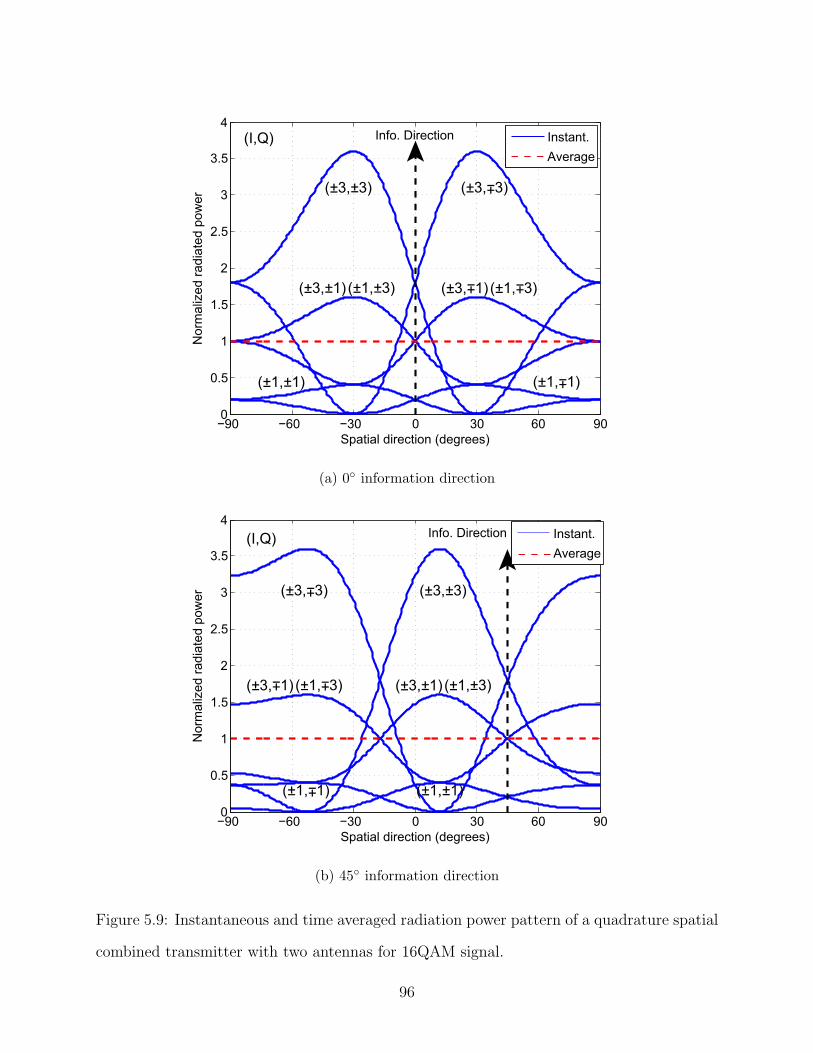
−90 −60 −30 0 30 60 900
0.5
1
1.5
2
2.5
3
3.5
4
Spatial direction (degrees)
Norm
aliz
ed r
adia
ted p
ow
er
Instant.Average
Info. Direction
( 3, 3)±±( 3, 3)±±
( 3, 1)±± ( 1, 3)±± ( 3, 1)±± ( 1, 3)±
±
( 1, 1)±± ( 1, 1)±±
(I,Q)
(a) 0 information direction
−90 −60 −30 0 30 60 900
0.5
1
1.5
2
2.5
3
3.5
4
Spatial direction (degrees)
Norm
aliz
ed r
adia
ted p
ow
er
Instant.Average
Info. Direction(I,Q)
( 3, 3)±± ( 3, 3)±±
( 3, 1)±± ( 1, 3)±
± ( 3, 1)±± ( 1, 3)±±
( 1, 1)±
± ( 1, 1)±±
(b) 45 information direction
Figure 5.9: Instantaneous and time averaged radiation power pattern of a quadrature spatial
combined transmitter with two antennas for 16QAM signal.
96

Figure 5.10: Multi-element beamforming transmitter with quadrature spatial combining.
The whole concept can be further extended to a beamforming transmitter where eachI/Q transmitter consists of multiple elements, as shown in Fig. 5.10. The information beamcan be steered along with the power beam of each I/Q antenna array. In a beamformingtransmitter with multiple PAs, there are several ways of implementing direct digital-to-RFconversion:
i). Digital PA only. In this scheme, each PA consists of a sub-PA array driven by thebaseband digital bits. The PAs in different elements are driven in the same manner by thesame digital bits. Hence the resolution of each PA is equal to the resolution of the entiretransmitter.
ii). Digital Antenna only. In this scheme, each PA is a 1-bit DAC, either on or off. Thedigital-to-RF conversion is achieved by turning on and off individual elements. Hence thenumber of antenna elements determines the amplitude resolution.
iii). Digital PA/Antenna. In this segmented approach, the LSB digital bits drive thefirst element sub-PA arrays while the MSB digital bits drive the PAs in other elements. Theresolution of the entire transmitter is the sum of the PA resolution and the number of theantenna elements.
The advantage of digitally switching antenna elements is higher amplitude resolution andtherefore lower output spectral noise floor.
97

Baseband DSP
15GHz LO
ØLOi4
PA
PA
ibbe<6>ibbl<6>
ØLOi3
PA
PA
ibbe<5>ibbl<5>
ØLOi2
PA
PA
ibbe<4>ibbl<4>
ØLOi1
PA
array
PA
array
ibbe<3:0>ibbl<3:0>ibbsign
I Array
TX-I-1
TX-I-2
TX-I-3
TX-I-4
FIR 2-fold
interp.Ser.PRBS ibbe<6:0>
ibbl<6:0>
ibbsign
FIR 2-fold
interp.Ser. PRBSqbbe<6:0>
qbbl<6:0>
qbbsign
X2
X2
ØLOq4
qbbe<6>qbbl<6>
PA
PA
ØLOq3
qbbe<5>qbbl<5>
PA
PA
ØLOq2
PA
PA
qbbe<4>qbbl<4>
ØLOq1
PA
array
PA
array
qbbe<3:0>qbbl<3:0>
qbbsign
Q Array
TX-Q-1
TX-Q-2
TX-Q-3
TX-Q-4
60GHz LO
LO Gen. Dist.
Figure 5.11: System block diagram of the 60GHz beamforming transmitter with quadrature
spatial combining.
5.4 Circuit Implementation
To demonstrate the concept, a 60GHz beamforming transmitter was implemented tar-geting WiGig applications. A segmented digital PA/antenna approach is chosen to achievehigher amplitude resolution. In this transmitter (Fig. 5.11), each I/Q array consists of 4elements, hence providing 2 bits of coarse amplitude resolution (bit 4-6). The PA in the firstelement in further segmented into 4 thermometer cells to provide 2 bits of fine amplituderesolution (bit 0-3). As a result, the total amplitude resolution is 4 bits for each I/Q ar-ray. Both coarse and fine digital bits are thermometer coded. The LO signal is distributedthrough a chain of lumped Wilkinson power dividers and LO phase shifters are used to lo-cally adjust the phase for beam steering as well as quadrature signal summation. Finally amixed-signal approach combining baseband DSP and two-fold linear interpolation is imple-mented for output spectral filtering. The details of each block are described in the followingsubsections.
98

5.4.1 mm-Wave Switching PA-DAC
The key advantage of the direct digital-to-RF conversion architecture is the ability to useswitching amplifier for higher PA efficiency. The most attractive switching amplifier class forhigh frequency applications is the Class-E/F family due to transistor capacitance tolerance[8]. It’s shown in Chapter. 2 that second harmonic tuning can significantly improve the PAefficiency, and such tuning class is known as Class-E/FX2 with optimal X2 being around0.5. Such tuning requires a passive matching network that can resonate with the transistordrain parasitic capacitance at both the fundamental and the second harmonic frequency.Implementing such a matching network usually involves several series or parallel branches,which not only increases the insertion loss at the fundamental frequency, but also reducesthe second harmonic content, as discussed in Chapter. 4 and [30]. Here we propose a simpletuning network that can achieve the desired impedance with minimum complexity. The keycomponent is a two turn inductor. When a two turn inductor is excited by differential signals,the magnetic flux generated by the two windings add constructively, as shown in Fig. 5.13a,therefore the total inductance is 4 times larger than that of a single turn inductor. On theother hand, if the two turn inductor is excited by common-mode signals, the magnetic fluxgenerated by the two windings cancel out each other, as shown in Fig. 5.13b, and the effectiveinductive area is the enclosed gap between the two windings. This means the common-modeinductance is much smaller than the differential-mode inductance. Since the second harmonicsignals in a differential PA are common-mode signals and the required second harmonic loadinductance is one quarter of the fundamental load inductance, a two turn inductor can satisfythe tuning requirement by properly adjusting the winding diameter/spacing and bypassingthe center tap. Fig. 5.12 shows the differential mode and common-mode inductance for atwo turn inductor with 25µm inner diameter and 2.5µm spacing. This inductor is usedas the primary side of a 2:1 transformer which performs differential to single-ended signalconversion. The V-I waveforms of the Class-E/F2 PA using the 2:1 transformer is shown inFig. 5.14 for both square wave input and sine wave input.
Fig. 5.15 shows the schematic of the 2-bit PA-DAC in the first transmitter element. ThePA is segmented into four thermometer sub-PA units for direct digital modulation, eachunit being a differential pair. The digital switching function is implemented by a bottomswitch connected to the source of a differential pair. Each switch is sized roughly twiceas large as the combined differential pair size so that the power degradation is reduced toless than 0.2dB. To compensate for the compressive AM-AM distortion present in a typicalPA, non-uniform device sizing is applied to the thermometer units. The sizes are chosen tominimize the DNL. Similar to an analog PA, this PA-DAC also exhibits AM-PM distortiondue to capacitance variation when the sub-PA units are being switched on and off. Tocompensate for this effect, a switched capacitor array is added at the differential input ofthe PA-DAC. One pair of switched capacitor is turned on when one sub-PA unit is turnedoff. The switched capacitor array has a unit size of 3.4fF and is binary coded. A bottomswitch is also inserted in the drive stage differential pair to completely turn off the driver inorder to minimize the signal leakage at code zero. This also reduces the power consumptionat back-off power levels and improves the efficiency. Finally, an identical copy of the 2-bitPA-DAC is connected in parallel, forming an early and late PA array pair. The late PA
99

20 40 60 80 100 120 140 160 1800
30
60
90
120
150
180
210
240
Frequency (GHz)
Inducta
nce (
pH
)
DIFF
CMMD
(a) Inductance
0 20 40 60 80 100 120 140 160 1800
3
6
9
12
15
Frequency (GHz)
Q−factor
DIFF
CMMD
(b) Q-factor
Figure 5.12: Inductance and Q-factor of a two turn inductor (25µm inner diameter and
2.5µm spacing).
100

(a) Differential mode
(b) Common mode
Figure 5.13: Magnetic field of a two-turn inductor when exited by differential signals and
common-mode signals
101

0 2 4 6 8 10 12 14 16 180
2
4
Time (ps)
Voltage (
V)
0 2 4 6 8 10 12 14 16 18−50
0
50
Curr
ent
(mA
)
drain voltage
gate voltage
drain current
(a) Square wave drive
0 2 4 6 8 10 12 14 16 180
2
4
Time (ps)
Voltage (
V)
0 2 4 6 8 10 12 14 16 18−50
0
50
drain voltage
gate voltage
drain current
Curr
ent
(mA
)
(b) Sine wave drive
Figure 5.14: V-I waveforms of the Class-E/F2 PA using 2:1 transformer.
102
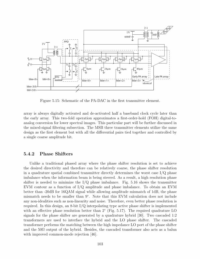
bbe<0>
1V
2:1
2:11V
bbe<3:0>
1x 2x
PPD
control
Late PA arrayEarly PA arraybbl<0>
identical
PPD
bbl<3:0>
bbe<0> bbe<1> bbe<2> bbe<3>
2.2µm 6.6µm 6.6µm 11µm
8µm 24µm 24µm 40µm
13µm
20µm
600fF30fF
S
G
G
Figure 5.15: Schematic of the PA-DAC in the first transmitter element.
array is always digitally activated and de-activated half a baseband clock cycle later thanthe early array. This two-fold operation approximates a first-order-hold (FOH) digital-to-analog conversion for lower spectral images. This particular part will be further discussed inthe mixed-signal filtering subsection. The MSB three transmitter elements utilize the samedesign as the first element but with all the differential pairs tied together and controlled bya single coarse amplitude bit.
5.4.2 Phase Shifters
Unlike a traditional phased array where the phase shifter resolution is set to achievethe desired directivity and therefore can be relatively coarse, the phase shifter resolutionin a quadrature spatial combined transmitter directly determines the worst case I/Q phaseimbalance when the information beam is being steered. As a result, a high resolution phaseshifter is needed to minimize the I/Q phase imbalance. Fig. 5.16 shows the transmitterEVM contour as a function of I/Q amplitude and phase imbalance. To obtain an EVMbetter than -20dB for 16QAM signal while allowing amplitude mismatch of 1dB, the phasemismatch needs to be smaller than 9. Note that this EVM calculation does not includeany non-idealities such as non-linearity and noise. Therefore, even better phase resolution isrequired. In this design, an 8-bit I/Q interpolating type active phase shifter is implementedwith an effective phase resolution better than 2 (Fig. 5.17). The required quadrature LOsignals for the phase shifter are generated by a quadrature hybrid [30]. Two cascaded 1:2transformers are used to interface the hybrid and the LO phase shifter. The cascadedtransformer performs the matching between the high impedance LO port of the phase shifterand the 50Ω output of the hybrid. Besides, the cascaded transformer also acts as a balunwith improved common-mode rejection [46].
103
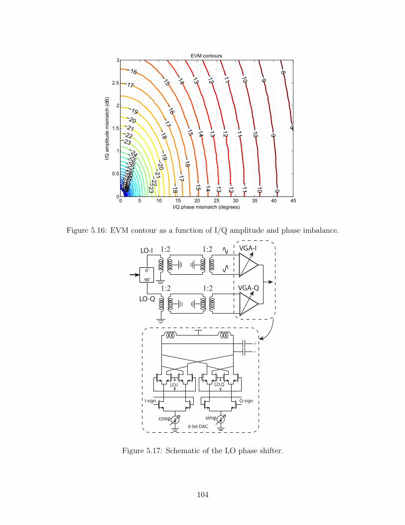
−37−36−35−34−33−32−31−30−29−28
−27−26
−25−24
−23
−23
−22
−22
−21
−21
−20
−20
−19
−19
−18
−18
−17
−17
−17
−16
−16
−16
−15
−15−15
−14
−14−14
−13
−13−13
−12
−12−12
−11
−11−11
−10−10
−10−9
−9−9
−8−8
I/Q phase mismatch (degrees)
I/Q
am
plit
ude m
ism
atc
h (
dB
)
EVM contours
0 5 10 15 20 25 30 35 40 450
0.5
1
1.5
2
2.5
3
Figure 5.16: EVM contour as a function of I/Q amplitude and phase imbalance.
+
-
LO-I 1:2 1:2 VGA-I
LO-Q
1:2 1:2 VGA-Q
0˚
90˚
LO.I LO.Q
cosφ sinφ
I-sign Q-sign
6-bit DAC
Figure 5.17: Schematic of the LO phase shifter.
104
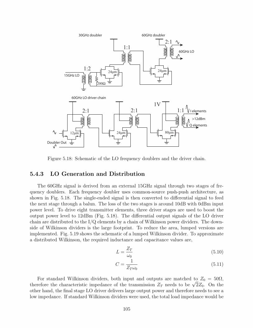
1:1
80μm
1V
2:1
24μm
2:1
24μm24μm
1:1
30GHz doubler 60GHz doubler
15GHz LO
I elements
>12dBm
60GHz LO driver chain
1:2
200Ω
12μm
2:1
60GHz LO
Q elements
Doubler Out
Figure 5.18: Schematic of the LO frequency doublers and the driver chain.
5.4.3 LO Generation and Distribution
The 60GHz signal is derived from an external 15GHz signal through two stages of fre-quency doublers. Each frequency doubler uses common-source push-push architecture, asshown in Fig. 5.18. The single-ended signal is then converted to differential signal to feedthe next stage through a balun. The loss of the two stages is around 10dB with 0dBm inputpower level. To drive eight transmitter elements, three driver stages are used to boost theoutput power level to 12dBm (Fig. 5.18). The differential output signals of the LO driverchain are distributed to the I/Q elements by a chain of Wilkinson power dividers. The down-side of Wilkinson dividers is the large footprint. To reduce the area, lumped versions areimplemented. Fig. 5.19 shows the schematic of a lumped Wilkinson divider. To approximatea distributed Wilkinson, the required inductance and capacitance values are,
L =ZT
ω0
(5.10)
C =1
ZTω0
(5.11)
For standard Wilkinson dividers, both input and outputs are matched to Z0 = 50Ω,therefore the characteristic impedance of the transmission ZT needs to be
√2Z0. On the
other hand, the final stage LO driver delivers large output power and therefore needs to see alow impedance. If standard Wilkinson dividers were used, the total load impedance would be
105
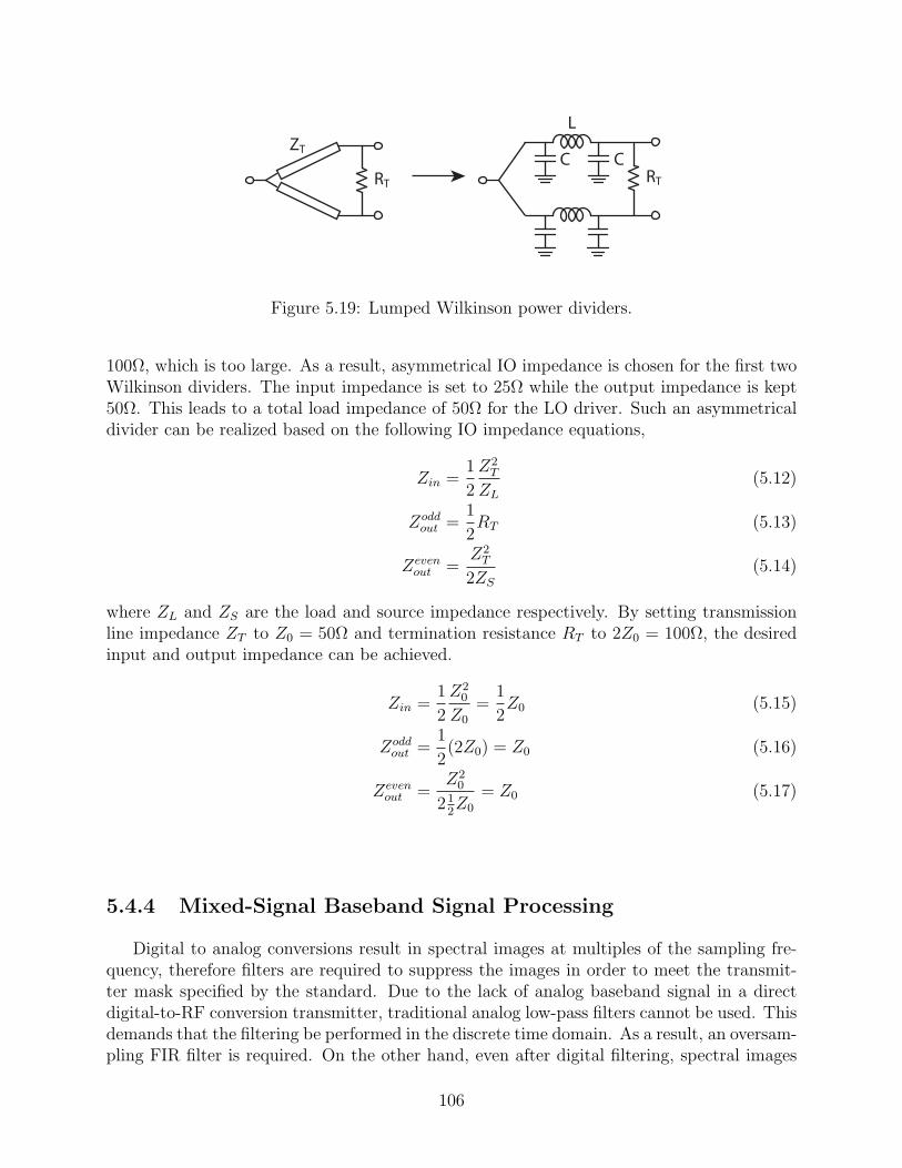
RT
ZT
L
C C
RT
Figure 5.19: Lumped Wilkinson power dividers.
100Ω, which is too large. As a result, asymmetrical IO impedance is chosen for the first twoWilkinson dividers. The input impedance is set to 25Ω while the output impedance is kept50Ω. This leads to a total load impedance of 50Ω for the LO driver. Such an asymmetricaldivider can be realized based on the following IO impedance equations,
Zin =1
2
Z2T
ZL
(5.12)
Zoddout =
1
2RT (5.13)
Zevenout =
Z2T
2ZS
(5.14)
where ZL and ZS are the load and source impedance respectively. By setting transmissionline impedance ZT to Z0 = 50Ω and termination resistance RT to 2Z0 = 100Ω, the desiredinput and output impedance can be achieved.
Zin =1
2
Z20
Z0
=1
2Z0 (5.15)
Zoddout =
1
2(2Z0) = Z0 (5.16)
Zevenout =
Z20
212Z0
= Z0 (5.17)
5.4.4 Mixed-Signal Baseband Signal Processing
Digital to analog conversions result in spectral images at multiples of the sampling fre-quency, therefore filters are required to suppress the images in order to meet the transmit-ter mask specified by the standard. Due to the lack of analog baseband signal in a directdigital-to-RF conversion transmitter, traditional analog low-pass filters cannot be used. Thisdemands that the filtering be performed in the discrete time domain. As a result, an oversam-pling FIR filter is required. On the other hand, even after digital filtering, spectral images
106

2 4 6 8 10 12 14 16 18 20−70
−60
−50
−40
−30
−20
−10
Oversampling rate
First
spectr
al im
age level (d
Bc)
ZOH
FOH
Figure 5.20: First spectral image level as a function of the oversampling rate.
0 0.2 0.4 0.6 0.8 1 1.2 1.4 1.6 1.8 2−60
−50
−40
−30
−20
−10
0
Normalized Frequency
Outp
ut
Spectr
um
(dB
c)
Zero−Order−Hold
First−Order−HoldTwo−Fold Interp.
Image window
Figure 5.21: Output spectrum of different types of digital to analog conversion.
107

still exist at multiples of the oversampled clock frequency. The largest spectral image levelof a Zero-Order-Hold (ZOH) digital to analog converter is a function of the oversamplingrate (OSR),
Pimage = 20 log(sinc(1− 1
2OSR))− 6 (5.18)
As the WiGig standard requires out-of-band emission lower than -30dBc, an oversamplingrate of 8 is required if traditional ZOH is used. However, running the digital filter at 14GHz(1.76G × 8) is impractical. In addition, distributing such high speed digital signals costssignificant power consumption. To remedy this problem, a mixed signal approach is used.Compared to traditional ZOH digital to analog conversion whose output spectrum exhibitsa sinc rolloff, FOH conversion exhibits a sinc2 rolloff and therefore provides additional sup-pression on the spectral image, as shown in Fig. 5.20. This means lower oversampling rateis required for the same image level. In this design, an oversampling rate of 4 is chosen.To simplify the implementation of a FOH conversion, multi-fold linear interpolation can beused as a close approximation [39]. Since the first spectral image is usually much larger thanother images, two-fold interpolation is sufficient to suppress this dominant image. Fig. 5.21compares the output spectrum of ZOH, FOH and two-fold interpolation. Clearly, both FOHand two-fold interpolation exhibit lower spectral amplitude than ZOH near the samplingfrequency, and the two-fold interpolation well matches the FOH within the spectral imagewindow. The implementation of the entire mixed-signal baseband signal processing unit isshown in Fig. 5.22. The FIR consists of four sub-FIRs, each running at the Nyquist samplingfrequency to reduce power consumption. A 4:1 serializer is used at the output to produce theoversampled data stream. The output of the serializer is divided into two parallel bit streams,an early signal and a late signal. Two-fold linear interpolation requires half baseband clockcycle delay between the two bit streams, which is achieved by adding one additional latch inthe late signal path. The early and late digital signals are distributed to eight transmitterelements to activate/de-activate the early and late PAs. A MUX is inserted to enable FIRand two-fold interpolation bypassing for comparison.
The detailed serializer schematic is shown in Fig. 5.23. It consists of two stages of 2:1serializers. Latches are inserted in front of the MUX in order to ensure the serializationsequence. Due to additional one latch delay, bits going through ”1” input of the MUXalways get serialized before bits going through ”0” input of the MUX. The 1x and 2x clocksare derived from two frequency dividers. Note that the frequency dividers need to be sharedbetween the I and Q baseband units in order to align the serialized I and Q data.
5.4.5 Supply Bypass Network
Due to dynamic current scaling, the supply voltage experiences significant ripples. Thesupply ripples are mainly caused by the inductance introduced by bondwires or micro-bumps.Since the supply ripple increases with the loop inductance, low inductance packaging suchas flip-chip is preferred. On the other hand, to minimize the impact of supply noise on thetransmitter EVM, the supply path needs to have a fast settling time. The supply bypass
108

sub-FIR-1
sub-FIR-2
sub-FIR-3
sub-FIR-4
4:1
Serializer
Nyquist clk 2x clk
bbl
L
bbe
0
1
0
1
FIRbypass
Two-fold linear
interpolation
/2/24x clk
L L
L L
BB
PRBS Late PA
Early PA
Figure 5.22: Mixed-signal baseband signal processing for spectrum filtering.
L
1
0
L
L
L
1
0
L
L
L
1
0
L
L
2x cp 2x cn
1x cp
1x cn
1x cn
1x cp
2x cp
d<0>
d<1>
d<2>
d<3>
d<0:4>
Figure 5.23: Schematic of the 4-to-1 serializer.
network can be modeled by a second order RLC circuit with a Q-factor of√
LC
1R. For a
given LC, the settling time can be minimized by setting the second order system slightlyoverdamped (Q≈1). Under that condition, the settling time can be approximated by,
ts ≈ln(ǫ)Q
ωn
=ln(ǫ)L
R(5.19)
where ǫ is the relative error tolerance. Apparently the settling time can be minimized byincreasing R. However, digital amplitude code switching results in delta pulses on the supplyvoltage and the pulse amplitude is proportional to R. As a result, R cannot be arbitrarily
109

PA
G
S
G
vdd
vss
PA S
vdd
G
vss
Figure 5.24: Supply bypass network floorplan.
increased. In this design, a series combination of 200pF bypass capacitor and 1.5Ω resistoris used for each transmitter element so that the worst-case voltage pulse is less than 250mVand the pulse can be settled within 350ps. Fig. 5.24 shows the bypass network floorplan.Each transmitter has a vdd/vss bump pad pair and the de-Qued bypass capacitor is placedbetween them.
5.5 Experimental Results
The beamforming transmitter is fabricated in a bulk 65nm CMOS technology with nospecial RF options and the die measures 3×3 mm2. Fig. 5.25 shows the chip micrograph.This section is divided into two parts. The first part describes the Continuous-Wave (CW)mode measurement results from on-die probing and the second part describes the modulationtest results from the mm-wave package.
110

Figure 5.25: Chip Micrograph.
111
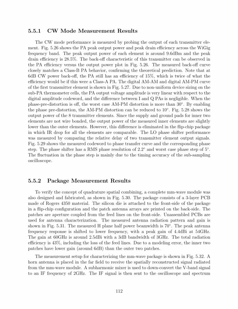
5.5.1 CW Mode Measurement Results
The CW mode performance is measured by probing the output of each transmitter ele-ment. Fig. 5.26 shows the PA peak output power and peak drain efficiency across the WiGigfrequency band. The peak output power of each element is around 9.6dBm and the peakdrain efficiency is 28.5%. The back-off characteristic of this transmitter can be observed inthe PA efficiency versus the output power plot in Fig. 5.26. The measured back-off curveclosely matches a Class-B PA behavior, confirming the theoretical prediction. Note that at6dB CW power back-off, the PA still has an efficiency of 15%, which is twice of what theefficiency would be if this were a Class-A PA. The digital AM-AM and digital AM-PM curveof the first transmitter element is shown in Fig. 5.27. Due to non-uniform device sizing on thesub-PA thermometer cells, the PA output voltage amplitude is very linear with respect to thedigital amplitude codeword, and the difference between I and Q PAs is negligible. When thephase-pre-distortion is off, the worst case AM-PM distortion is more than 30. By enablingthe phase pre-distortion, the AM-PM distortion can be reduced to 10. Fig. 5.28 shows theoutput power of the 8 transmitter elements. Since the supply and ground pads for inner twoelements are not wire bonded, the output power of the measured inner elements are slightlylower than the outer elements. However, this difference is eliminated in the flip-chip packagein which IR drop for all the elements are comparable. The LO phase shifter performancewas measured by comparing the relative delay of two transmitter element output signals.Fig. 5.29 shows the measured codeword to phase transfer curve and the corresponding phasestep. The phase shifter has a RMS phase resolution of 2.2 and worst case phase step of 5.The fluctuation in the phase step is mainly due to the timing accuracy of the sub-samplingoscilloscope.
5.5.2 Package Measurement Results
To verify the concept of quadrature spatial combining, a complete mm-wave module wasalso designed and fabricated, as shown in Fig. 5.30. The package consists of a 3-layer PCBmade of Rogers 4350 material. The silicon die is attached to the front-side of the packagein a flip-chip configuration and the patch antenna arrays are printed on the back-side. Thepatches are aperture coupled from the feed lines on the front-side. Unassembled PCBs areused for antenna characterization. The measured antenna radiation pattern and gain isshown in Fig. 5.31. The measured H plane half power beamwidth is 70. The peak antennafrequency response is shifted to lower frequency, with a peak gain of 4.4dBi at 54GHz.The gain at 60GHz is around 2.5dBi with a 3dB bandwidth of 3GHz. The total radiationefficiency is 43%, including the loss of the feed lines. Due to a modeling error, the inner twopatches have lower gain (around 6dB) than the outer two patches.
The measurement setup for characterizing the mm-wave package is shown in Fig. 5.32. Ahorn antenna is placed in the far field to receive the spatially reconstructed signal radiatedfrom the mm-wave module. A subharmonic mixer is used to down-convert the V-band signalto an IF frequency of 2GHz. The IF signal is then sent to the oscilloscope and spectrum
112

57 58 59 60 61 62 63 645
10
15
20
25
30
Frequency (GHz)
PA
outp
ut
pow
er
(dB
m)
/ E
ffic
iency (
%)
Pout
Efficiency
(a)
0 2 4 6 8 100
5
10
15
20
25
30
PA output power (mW)
PA
Eff
icie
ncy (
%)
meas. PA
Class−AClass−B
(b)
Figure 5.26: Measured transmitter output power and drain efficiency.
113

0 1 2 3 40
200
400
600
800
1000
Digital codeword
PA
outp
ut
voltage a
mplit
ude (
mV
)
PA−IPA−Q
(a)
1 2 3 4−10
0
10
20
30
40
Input codeword
PM
(degre
es)
PPD off
PPD on
(b)
Figure 5.27: Measured first transmitter digital AM-AM and digital AM-PM behaviors.
114

57 58 59 60 61 62 63 64 654
5
6
7
8
9
10
Frequency (GHz)
TX
ele
ment
outp
ut
pow
er
(dB
m)
I1 I2 I3 I4 Q1 Q2 Q3 Q4
Figure 5.28: Measured output power of 8 transmitter elements.
0 8 16 24 32 40 48 56 64−10
0
10
20
30
40
50
60
70
80
90
Codeword
Phase (
degre
es)
phase
step
Figure 5.29: Measured LO phase shifter codeword to phase transfer curve and the corre-
sponding phase step.
115

Package frontside Package backside
I/Q antenna arrays
ip-chip
Figure 5.30: Flip-chip packaged module with antenna arrays.
-30
-20
-10
0
10
30
210
60
240
90
270
120
300
150
330
180 0
50 52 54 56 58 60 62 64 66−20
−15
−10
−5
0
5
10
Frequency (GHz)
Gain
(dB
i)
Element−1Element−2Element−3Element−4
Figure 5.31: Measured antenna radiation pattern and freqeuncy response.
analyzer for EVM and spectrum analysis. A V-band power meter is also used to measurethe EIRP and the digital AM- RF AM curve.
The measured peak EIRP is 22dBm at 60GHz in the broadside direction. Fig. 5.33shows the digital AM - RF AM curve of the entire transmitter array, which is normalizedto the peak value (22dBm). It can be observed that the curve is piece-wise linear within4 codes, re-confirming the probing measurement results. However, due to reduced antennagain of the inner two patches, the AM-AM curve exhibits two non-monotonicity at code5 and code 9. Although these codewords are avoided at Nyquist samples by digital pre-distortion to prevent EVM degradation, there are residual effects such as spectral re-growthand increased out-of-band emission. This error can be eliminated once the inner patches areproperly redesigned.
116

txLO=15GHz rxLO=14.5GHz
v-band 4th order
sub-harmonic
down-converter
signal generator signal generator
oscilloscope
mm-wave
ip-chip package
horn antenna IF=2GHz
v-band
power meter
EIRP/power
measurement
EVM
measurement
refclk
IQ
PC
d > 350mm
SPI
signal generator
txBBclk
refclk
Figure 5.32: Measurement setup for wireless transmission using the mm-wave module.
0 2 4 6 8 10 12 14 160
0.1
0.2
0.3
0.4
0.5
0.6
0.7
0.8
0.9
1
Codeword
Norm
aliz
ed o
utp
ut
am
plit
ude
Figure 5.33: Measured radiated transmitter amplitude as a function of amplitude codeword.
117

−2 −1.5 −1 −0.5 0 0.5 1 1.5 2−2
−1.5
−1
−0.5
0
0.5
1
1.5
2Data−rate: 3.5Gb/s
Figure 5.34: Received signal constellation for QPSK modulation at 3.5Gb/s.
−1.5 −1 −0.5 0 0.5 1 1.5−1.5
−1
−0.5
0
0.5
1
1.5Data−rate: 6Gb/s
Figure 5.35: Received signal constellation for 16QAM modulation at 6Gb/s.
118

−10 −5 0 5 10−30
−25
−20
−15
−10
−5
0
Receiving angle (degrees)
rms E
VM
(dB
)
Theoretical
Measured
Figure 5.36: Transmitter output EVM as a function of spatial angle.
Modulated signal transmission was conducted by sending an I/Q pseudo random bit se-quence (PRBS) from the transmitter and recovering the data by the aforementioned externalreceiver. Fig. 5.34 plots the received signal constellation for QPSK modulation at 3.5Gb/sdata rate with a carrier frequency of 60GHz. The corresponding EVM is -15dB. Similarly,the constellation for 16QAM modulation is shown in Fig. 5.35. The data rate for 16QAMmodulation is 6Gb/s and the EVM is -16.2dB. The average EIRP is around 16.4dBm. Thetransmitter EVM was also tested as a function of the receiving angle. Fig. 5.36 showsthe measured EVM pattern when the information direction is centered around 0. QPSKmodulation is used in this experiment with a carrier frequency of 60GHz and a data rate of2Gb/s. The measured EVM spatial behavior matches closely with the theoretical prediction.Finally, the mixed-signal baseband signal processing function is verified by monitoring thetransmitter output spectrum. Fig. 5.37 and Fig. 5.38 show the downconverted output spec-trum for QPSK and 16QAM modulation schemes respectively. Comparing the spectrumsbefore and after the FIR and interpolation are turned on, it’s clear that the mixed-signalbaseband signal processing can effectively suppress the image and lower the noise floor. Withmixed-signal filtering on, the output spectrum is compliant with the WiGig mask.
The entire circuit is powered from 1V supplies. The I/Q PA arrays consume a peakDC power of 229mW and the entire transmitter consumes a peak power of 382mW. Thepower consumption of other blocks are summarized in Table. 5.1. The measured peak PAefficiency is 28.5% and the peak transmitter efficiency is 17.4%. The average efficiency of
119
0 0.5 1 1.5 2 2.5 3 3.5 4−50
−40
−30
−20
−10
0
10
Offset Frequency (GHz)
Norm
aliz
ed o
utp
ut
spectr
um
(dB
m)
WiGig Mask
(a) FIR and Interp OFF
0 0.5 1 1.5 2 2.5 3 3.5 4−50
−40
−30
−20
−10
0
10
Offset Frequency (GHz)
Norm
aliz
ed o
utp
ut
spectr
um
(dB
m)
WiGig Mask
(b) FIR and Interp ON
Figure 5.37: Measured QPSK transmitter output spectrum.
120

0 0.5 1 1.5 2 2.5 3 3.5 4−50
−40
−30
−20
−10
0
10
Offset Frequency (GHz)
Norm
aliz
ed o
utp
ut
spectr
um
(dB
m)
WiGig Mask
(a) FIR and Interp OFF
0 0.5 1 1.5 2 2.5 3 3.5 4−50
−40
−30
−20
−10
0
10
Offset Frequency (GHz)
Norm
aliz
ed o
utp
ut
spectr
um
(dB
m)
WiGig Mask
(b) FIR and Interp ON
Figure 5.38: Measured 16QAM transmitter output spectrum.
121

Block Power (mW)PA 229Phase Shifter 48BB Signal Processing 40BB Signal Distribution 30LO Drivers 35Total 382
Table 5.1: Chip power breakdown.
CW ModePeak EIRP (dBm) 22TX Element Pout (dBm) 9.6PA peak efficiency (%) 28.5TX peak efficiency (%) 17.4Total peak DC power (mW) 382Data transmission at 6dB backoffPA average efficiency (%) 16.5TX average efficiency (%) 7Peak data rate (Gb/s) 6QPSK EVM -1516QAM EVM -16.2TX average DC power (mW) 260
Table 5.2: Chip performance summary.
the transmitter is defined by the following equation,
ηaverage = ηpeakEIRPaverage
EIRPpeak
PDC,peak
PDC,average
(5.20)
where ηpeak is the peak efficiency of the transmitter, which can be measured by probing theCW output power of each transmitter. Note that EIRP is used instead of total output powerto account for the antenna array gain change in such a digital antenna system during thetransmission of a modulated signal. In a single antenna transmitter, the equation falls backto the original form,
ηaverage = ηpeakPo,average
Po,peak
PDC,peak
PDC,average
=Po,average
PDC,average
(5.21)
At 6dB back-off when transmitting QPSK or 16QAM data, the measured average PAefficiency is 16.5% and the average transmitter efficiency is 7%, based on Eq. 5.20. Table. 5.2
122

[37] [38] [47] This WorkTX architecture Outphasing Outphasing Class-AB Cartesian
digital-to-RFSignal reconstruction Spatial Transformer No need Spatial
combining combining combiningSingle PA Psat 9.7 15.6 10 9.6(dBm)ηPA at Psat (%) 11 25 10.8 28.5ηPA at 6dB BOa (%) N.A. 9 5.7b 15TX beamforming? Yes No No Yes
(2 PAs) (8 PAs)Antenna package? No No No Yes
(EIRP=22dBm)Modulation 16QAM 16QAM 16QAM 16QAMPeak data rate 0.2 0.5 7 6(Gb/s)Technology 65nm 40nm 40nm 65nm
Table 5.3: Comparison to efficiency enhancing 60GHz transmitters.
aCW modebAt 5dB back-off
summarizes the chip performance and Table. 5.3 compares this work to other state-of-the-art 60GHz transmitters with various efficiency enhancing techniques. Clearly, substantialimprovement has been achieved in terms of average efficiency.
5.6 Digital Calibration and Pre-distortion
Digital pre-distortion and calibration are required to linearize and compensate the directdigital-to-RF transmitter, as a result it’s critical to analyze all the potential non-idealitiesand figure out the corresponding algorithms. Some non-idealities in this architecture arecommon to those in traditional phased array transmitters or single-element transmitters andtherefore can be corrected by existing algorithms while others require additional training orcalibration.
As evident in the measurement results, the largest mismatch in the systems comes fromantenna mismatch, due to PCB manufacturing tolerances. This affects the transmitterperformance in a number of ways.
Gain mismatch between I and Q antennas results in I/Q amplitude imbalance, whichis a common issue in any transmitter. This can be calibrated either in the digital domain
123
by re-adjusting the full-scale of each I/Q DAC or in the analog domain by re-adjustingthe LO amplitude. Gain mismatch within each antenna array (between four patches in theprototype) results in AM-AM non-linearity. This can be corrected by digital pre-distortionthrough a LUT. Note that since I/Q arrays are de-coupled, the pre-distortion is only onedimensional. Since the antenna elements are unlikely to see identical environment, gainmismatch can be angle dependent. As a result, both I/Q amplitude imbalance and DACAM-AM non-linearity can be angle dependent. To address this issue, both calibration and1-D digital pre-distortion can be performed in different angles. Beam steering is usuallysectorized in a typical phased array, and a LUT may be loaded with different values fordifferent sectors.
The antenna mismatch can be also frequency dependent. The frequency dependent gainmismatch between I and Q antennas results in non-flat channel frequency response, and isno different from frequency dependent gain mismatch between I and Q circuitry on the chip.Such mismatch can be either compensated by a pre-emphasis filter [48] or lumped into thewireless channel response and corrected by the receiver equalizer.
The correction for frequency dependent gain mismatch within each antenna array is moresubtle. Note that three different schemes of digital-to-RF conversion implementation in abeamforming array are proposed. For Digital PA only scheme, different antenna elementsinside the same array is transmitting the same signal (either I or Q modulated signal),with only a relative delay, therefore frequency dependent gain mismatch only results innon-flat channel frequency response. This is the same problem that every phased arraysystem faces, and it can be corrected by pre-emphasis or receiver equalizer. For the DigitalAntenna only scheme and the mixed Digital PA/Antenna scheme, frequency dependent gainmismatch results in both non-flat channel frequency response and non-linearity. In this case,a MMSE algorithm may be used to minimize the EVM for all the possible symbols, whichis a potentially more involving task.
Another important design choice is regarding where the digital pre-distortion should beimplemented. In this implementation, digital pre-distortion was only applied to Nyquist ratesamples preceding the mixed-signal filtering unit. As a result, linearization is only effectiveat Nyquist rate samples 5. This is effective in improving EVM, but much less effective inreducing spectral regrowth and out-of-band emissions, especially when the non-linearity ofthe digital AM - RF AM transfer function is severe. A better approach is to place thedigital pre-distortion after filtering. This ensures that the oversampled digital codewords arecompletely linear, and both the EVM and spectral regrowth can be minimized. The price ofsuch an approach is increased power consumption and slightly reduced DAC resolution.
5Assuming the transmitter has sufficient bandwidth to preserve the Nyquist rate samples
124

Chapter 6
Conclusions
This dissertation focuses on the architecture and the implementation of efficient mm-wave wireless transmitters in standard CMOS technologies for both regional and personalarea networks. Low breakdown voltage and scarce power gain of the CMOS process havebeen identified as the main contributors to inferior transmitter performance at mm-wave.
To overcome the low supply voltage imposed by the breakdown voltage, transformerpower combining techniques are proposed and analyzed. A 65nm 60GHz PA utilizing aquad-input DAT was designed and fabricated. Measurement results prove that by doublingthe number of input ports in the combiner, the PA output power can be quadruped withoutsacrificing the efficiency. Given a particular CMOS process, maximum obtainable outputpower based on such type of combiners can be predicted. To further extend the rangeof a mm-wave wireless link, beamforming using spatial power combining can be utilized.Four types of beamforming radio architectures have been analyzed and compared. Analogbaseband beamforming was chosen as an optimal architecture for an 4-element transceiverarray design. The 65nm prototype achieves low power consumption.
Besides obtaining higher output power and peak efficiency, improving average efficiencyis equally important as most modulation schemes used today present non-constant envelopesignals. A key concept of digital quadrature spatial combing was introduced as an enabler forhighly efficient mm-wave transmitters. The direct digital-to-RF conversion architecture canimprove the transmitter peak efficiency by using non-linear class PAs and enhance the back-off efficiency by dynamically scaling the total DC power consumption according to the signalenvelope. At the same time, proposed quadrature spatial combining effectively eliminatesthe tradeoff between low insertion loss and high isolation associated with on-chip signalcombiners while does not create average spatial directivity. A 60GHz 4I+4Q beamformingtransmitter was designed, packaged and characterized. The transmitter delivers a peakEIRP of 22dBm at a power consumption of 382mW. At 6dB back-off when transmittingmodulated signals (QPSK/16QAM), the PA achieves an average efficiency of 16.5% with atotal transmitter average efficiency of 7%. A mixed-signal filtering approach consisting of
125

a 4x oversampling FIR and two-fold linear interpolation was used to suppress the spectralimages. The measured average PA efficiency at 6-dB back-off is 1.7× better than the state-of-the-art efficiency enhancing mm-wave transmitters.
126

Bibliography
[1] ERICSSON, “Traffic and market report,” 2012. [Online]. Available: http://www.ericsson.com/res/docs/2012/traffic and market report june 2012.pdf
[2] ITRS, “Itrs reports,” 2012. [Online]. Available: http://www.itrs.net/reports.html
[3] Y. Palaskas, A. Ravi, S. Pellerano, B. Carlton, M. Elmala, R. Bishop, G. Banerjee,R. Nicholls, S. Ling, N. Dinur, S. Taylor, and K. Soumyanath, “A 5-ghz 108-mb/s 2 2mimo transceiver rfic with fully integrated 20.5-dbm power amplifiers in 90-nm cmos,”Solid-State Circuits, IEEE Journal of, vol. 41, no. 12, pp. 2746–2756, Dec. 2006.
[4] G. D. Ewing, “High-efficiency radio-frequency power amplifiers,” Ph.D. dissertation,Oregon State University.
[5] N. Sokal and A. Sokal, “Class e-a new class of high-efficiency tuned single-ended switch-ing power amplifiers,” Solid-State Circuits, IEEE Journal of, vol. 10, no. 3, pp. 168–176,Jun 1975.
[6] M. Acar, A. Annema, and B. Nauta, “Analytical design equations for class-e poweramplifiers,” Circuits and Systems I: Regular Papers, IEEE Transactions on, Dec. 2007.
[7] F. Raab, “Idealized operation of the class e tuned power amplifier,” Circuits and Sys-tems, IEEE Transactions on, Dec. 1977.
[8] S. Kee, “The class e/f family of harmonic-tuned switching power amplifiers,” Ph.D.dissertation, California Institute of Technology.
[9] I. Aoki, S. Kee, D. Rutledge, and A. Hajimiri, “Distributed active transformer-a newpower-combining and impedance-transformation technique,” Microwave Theory andTechniques, IEEE Transactions on, Jan. 2002.
[10] M. Tanomura, Y. Hamada, S. Kishimoto, M. Ito, N. Orihashi, K. Maruhashi, andH. Shimawaki, “Tx and rx front-ends for 60ghz band in 90nm standard bulk cmos,” inSolid-State Circuits Conference, 2008. ISSCC 2008. Digest of Technical Papers. IEEEInternational, Feb. 2008.
[11] M. Bohsali and A. Niknejad, “Current combining 60ghz cmos power amplifiers,” inRadio Frequency Integrated Circuits Symposium, 2009. RFIC 2009. IEEE, June 2009.
127

[12] M. Y. Bohsali, “Millimeter - wave cmos power amplifiers design,” Ph.D. dissertation,University of California, Berkeley.
[13] C. Law and A.-V. Pham, “A high-gain 60ghz power amplifier with 20dbm output powerin 90nm cmos,” in Solid-State Circuits Conference Digest of Technical Papers (ISSCC),2010 IEEE International, Feb. 2010, pp. 426–427.
[14] D. Chowdhury, “Efficient transmitters for wireless communications in nanoscale cmostechnology,” Ph.D. dissertation, University of California, Berkeley.
[15] D. Chowdhury, P. Reynaert, and A. Niknejad, “A 60ghz 1v + 12.3dbm transformer-coupled wideband pa in 90nm cmos,” in Solid-State Circuits Conference, 2008. ISSCC2008. Digest of Technical Papers. IEEE International, Feb. 2008, pp. 560–635.
[16] C. Marcu, D. Chowdhury, C. Thakkar, J.-D. Park, L.-K. Kong, M. Tabesh, Y. Wang,B. Afshar, A. Gupta, A. Arbabian, S. Gambini, R. Zamani, E. Alon, and A. Niknejad,“A 90 nm cmos low-power 60 ghz transceiver with integrated baseband circuitry,” Solid-State Circuits, IEEE Journal of, vol. 44, no. 12, pp. 3434–3447, Dec. 2009.
[17] T. LaRocca and M.-C. Chang, “60ghz cmos differential and transformer-coupled poweramplifier for compact design,” in Radio Frequency Integrated Circuits Symposium, 2008.RFIC 2008. IEEE, 17 2008-April 17, pp. 65–68.
[18] I. Aoki, S. Kee, D. Rutledge, and A. Hajimiri, “Fully integrated cmos power amplifierdesign using the distributed active-transformer architecture,” Solid-State Circuits, IEEEJournal of, vol. 37, no. 3, pp. 371–383, Mar. 2002.
[19] C. A. Balanis, ANTENNA THEORY ANALYSIS AND DESIGN. John Wiley & Sons,2005.
[20] A. Natarajan, B. Floyd, and A. Hajimiri, “A bidirectional rf-combining 60ghz phased-array front-end,” in Solid-State Circuits Conference, 2007. ISSCC 2007. Digest of Tech-nical Papers. IEEE International, 2007, pp. 202–597.
[21] A. Natarajan, S. Reynolds, M.-D. Tsai, S. Nicolson, J.-H. Zhan, D. G. Kam, D. Liu,Y.-L. Huang, A. Valdes-Garcia, and B. Floyd, “A fully-integrated 16-element phased-array receiver in sige bicmos for 60-ghz communications,” Solid-State Circuits, IEEEJournal of, vol. 46, no. 5, pp. 1059–1075, 2011.
[22] A. Valdes-Garcia, S. Nicolson, J.-W. Lai, A. Natarajan, P.-Y. Chen, S. Reynolds, J.-H.Zhan, D. Kam, D. Liu, and B. Floyd, “A fully integrated 16-element phased-array trans-mitter in sige bicmos for 60-ghz communications,” Solid-State Circuits, IEEE Journalof, vol. 45, no. 12, pp. 2757–2773, 2010.
[23] K. Raczkowski, W. De Raedt, B. Nauwelaers, and P. Wambacq, “A wideband beam-former for a phased-array 60ghz receiver in 40nm digital cmos,” in Solid-State CircuitsConference Digest of Technical Papers (ISSCC), 2010 IEEE International, 2010, pp.40–41.
128

[24] H. Wang and A. Hajimiri, “A wideband cmos linear digital phase rotator,” in CustomIntegrated Circuits Conference, 2007. CICC ’07. IEEE, 2007, pp. 671–674.
[25] K. Doris, E. Janssen, C. Nani, A. Zanikopoulos, and G. Van Der Weide, “A 480 mw2.6 gs/s 10b time-interleaved adc with 48.5 db sndr up to nyquist in 65 nm cmos,”Solid-State Circuits, IEEE Journal of, vol. 46, no. 12, pp. 2821–2833, 2011.
[26] D. Stepanovic and B. Nikolic, “A 2.8gs/s 44.6mw time-interleaved adc achieving 50.9dbsndr and 3db effective resolution bandwidth of 1.5ghz in 65nm cmos,” in VLSI Circuits(VLSIC), 2012 Symposium on, 2012, pp. 84–85.
[27] E. A. Firouzjaei, “mm-wave phase shifters and switches,” Ph.D. dissertation, Universityof California, Berkeley.
[28] M. Tabesh, A. Arbabian, and A. Niknejad, “60ghz low-loss compact phase shifters usinga transformer-based hybrid in 65nm cmos,” in Custom Integrated Circuits Conference(CICC), 2011 IEEE, 2011, pp. 1–4.
[29] L. Kong, “Energy-efficient 60ghz phased-array design for multi-gb/s communicationsystems,” Ph.D. dissertation, University of California, Berkeley.
[30] M. Tabesh, J. Chen, C. Marcu, L. Kong, S. Kang, A. Niknejad, and E. Alon, “A 65nm cmos 4-element sub-34 mw/element 60 ghz phased-array transceiver,” Solid-StateCircuits, IEEE Journal of, vol. 46, no. 12, pp. 3018–3032, 2011.
[31] J. Chen and A. Niknejad, “A compact 1v 18.6dbm 60ghz power amplifier in 65nmcmos,” in Solid-State Circuits Conference Digest of Technical Papers (ISSCC), 2011IEEE International, 2011, pp. 432–433.
[32] J.-W. Lai and A. Valdes-Garcia, “A 1v 17.9dbm 60ghz power amplifier in standard65nm cmos,” in Solid-State Circuits Conference Digest of Technical Papers (ISSCC),2010 IEEE International, 2010, pp. 424–425.
[33] F. Wang, A. Yang, D. Kimball, L. Larson, and P. Asbeck, “Design of wide-bandwidthenvelope-tracking power amplifiers for ofdm applications,” Microwave Theory and Tech-niques, IEEE Transactions on, vol. 53, no. 4, pp. 1244–1255, 2005.
[34] D. Cox, “Linear amplification with nonlinear components,” Communications, IEEETransactions on, vol. 22, no. 12, pp. 1942–1945, 1974.
[35] H. Chireix, “High power outphasing modulation,” Radio Engineers, Proceedings of theInstitute of, vol. 23, no. 11, pp. 1370–1392, 1935.
[36] S. Moloudi and A. Abidi, “The outphasing rf power amplifier: A comprehensive analysisand a class-b cmos realization,” Solid-State Circuits, IEEE Journal of, vol. 48, no. 6,pp. 1357–1369, 2013.
[37] C. Liang and B. Razavi, “Transmitter linearization by beamforming,” Solid-State Cir-cuits, IEEE Journal of, vol. 46, no. 9, pp. 1956–1969, 2011.
129
[38] D. Zhao, S. Kulkarni, and P. Reynaert, “A 60-ghz outphasing transmitter in 40-nmcmos,” Solid-State Circuits, IEEE Journal of, vol. 47, no. 12, pp. 3172–3183, 2012.
[39] A. Kavousian, D. Su, M. Hekmat, A. Shirvani, and B. Wooley, “A digitally modulatedpolar cmos power amplifier with a 20-mhz channel bandwidth,” Solid-State Circuits,IEEE Journal of, vol. 43, no. 10, pp. 2251–2258, 2008.
[40] D. Chowdhury, L. Ye, E. Alon, and A. Niknejad, “An efficient mixed-signal 2.4-ghzpolar power amplifier in 65-nm cmos technology,” Solid-State Circuits, IEEE Journalof, vol. 46, no. 8, pp. 1796–1809, 2011.
[41] L. Ye, “Design and analysis of digitally modulated transmitters for efficiency enhance-ment,” Ph.D. dissertation, University of California, Berkeley.
[42] C. Lu, H. Wang, C. Peng, A. Goel, S. Son, P. Liang, A. Niknejad, H. Hwang, andG. Chien, “A 24.7dbm all-digital rf transmitter for multimode broadband applicationsin 40nm cmos,” in Solid-State Circuits Conference Digest of Technical Papers (ISSCC),2013 IEEE International, 2013, pp. 332–333.
[43] A. Niknejad, D. Chowdhury, J. Chen, J. Park, and L. Ye, “mm-wavequadrature spatial power combinig: A proposal,” July 2010. [Online]. Available:http://www.eecs.berkeley.edu/Pubs/TechRpts/2010/EECS-2010-110.pdf
[44] J. Chen, L. Ye, D. Titz, F. Gianesello, R. Pilard, A. Cathelin, F. Ferrero, C. Luxey,and A. M. Niknejad, “A digitally modulated mm-wave cartesian beamforming trans-mitter with quadrature spatial combining,” in Solid-State Circuits Conference Digest ofTechnical Papers (ISSCC), 2013 IEEE International, 2013, pp. 232–233.
[45] A. Babakhani, D. Rutledge, and A. Hajimiri, “Transmitter architectures based on near-field direct antenna modulation,” Solid-State Circuits, IEEE Journal of, vol. 43, no. 12,pp. 2674–2692, 2008.
[46] S. Emami, R. Wiser, E. Ali, M. Forbes, M. Gordon, X. Guan, S. Lo, P. McElwee,J. Parker, J. Tani, J. Gilbert, and C. Doan, “A 60ghz cmos phased-array transceiverpair for multi-gb/s wireless communications,” in Solid-State Circuits Conference Digestof Technical Papers (ISSCC), 2011 IEEE International, 2011, pp. 164–166.
[47] V. Vidojkovic, G. Mangraviti, K. Khalaf, V. Szortyka, K. Vaesen, W. Van Thillo, B. Par-vais, M. Libois, S. Thijs, J. Long, C. Soens, and P. Wambacq, “A low-power 57-to-66ghztransceiver in 40nm lp cmos with -17db evm at 7gb/s,” in Solid-State Circuits Confer-ence Digest of Technical Papers (ISSCC), 2012 IEEE International, 2012, pp. 268–270.
[48] T. Tsukizawa, N. Shirakata, T. Morita, K. Tanaka, J. Sato, Y. Morishita, M. Kanemaru,R. Kitamura, T. Shima, T. Nakatani, K. Miyanaga, T. Urushihara, H. Yoshikawa,T. Sakamoto, H. Motozuka, Y. Shirakawa, N. Yosoku, A. Yamamoto, R. Shiozaki, andN. Saito, “A fully integrated 60ghz cmos transceiver chipset based on wigig/ieee802.11adwith built-in self calibration for mobile applications,” in Solid-State Circuits ConferenceDigest of Technical Papers (ISSCC), 2013 IEEE International, 2013, pp. 230–231.
130