test structures for millimeter- wave cmos circuit … okada lab. test structures for millimeter-...
TRANSCRIPT
2010/03/22Matsuzawa& Okada Lab.
Test Structures for Millimeter- Wave CMOS Circuit Design
Kenichi Okada
Tokyo Institute of Technology, Japan
2010/03/22 K. Okada, Tokyo Tech
1
Matsuzawa& Okada Lab.
Outline
• Motivation• Issues for mmW CMOS Circuits• Device Characterization• De-embedding• Conclusion
2010/03/22 K. Okada, Tokyo Tech
2
Matsuzawa& Okada Lab.
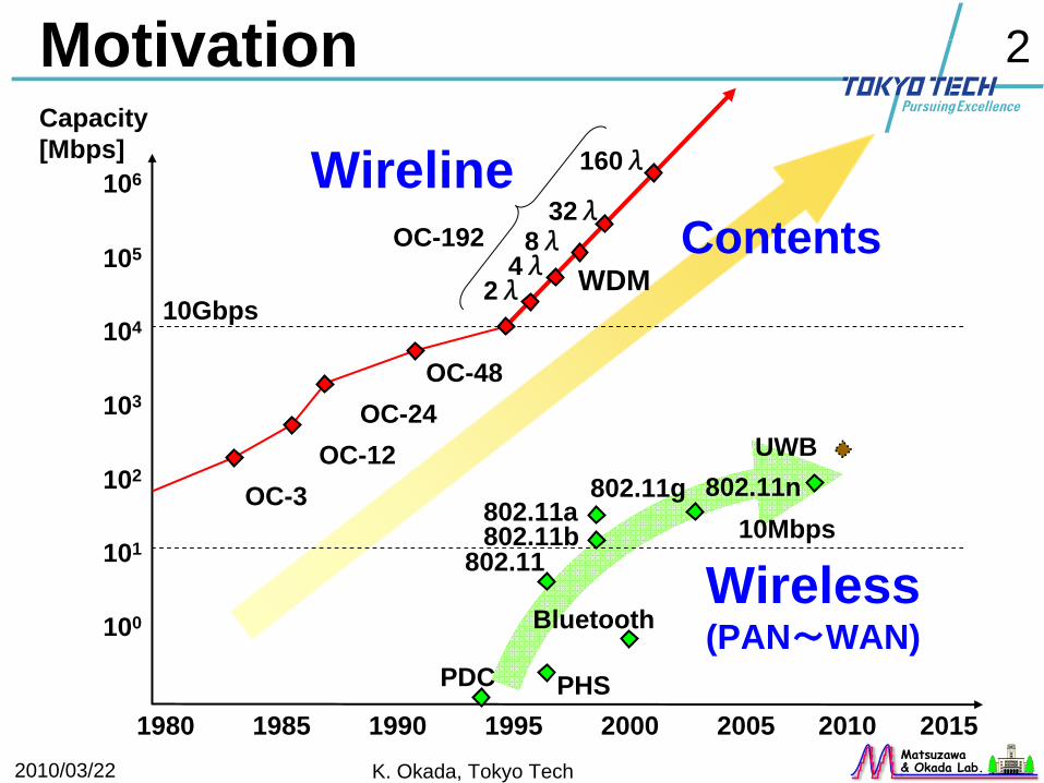
Motivation
1980 1985 1990 1995 2000 2005 2010 2015
101
102
103
104
105
106
WDMOC-192
2λ4λ
8λ32λ
160λCapacity[Mbps]
OC-48OC-24
OC-12OC-3
Wireline
802.11802.11b802.11a
802.11g 802.11nUWB
100 Bluetooth
PHSPDC
10Mbps
Wireless(PAN~WAN)
10Gbps
Contents
2010/03/22 K. Okada, Tokyo Tech
3
Matsuzawa& Okada Lab.
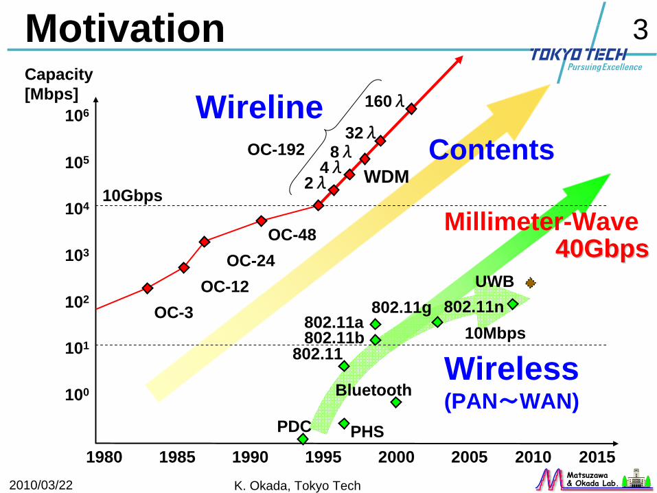
Motivation
1980 1985 1990 1995 2000 2005 2010 2015
101
102
103
104
105
106
WDMOC-192
2λ4λ
8λ32λ
160λ
40Gbps40Gbps
Capacity[Mbps]
OC-48OC-24
OC-12OC-3
Wireline
802.11802.11b802.11a
802.11g 802.11nUWB
100 Bluetooth
PHSPDC
Millimeter-Wave
10Mbps
Wireless(PAN~WAN)
10Gbps
Contents
2010/03/22 K. Okada, Tokyo Tech
4
Matsuzawa& Okada Lab.
Frequency [GHz]10 20 30 60 100 200 300
0.1
1
10
100
0.01
Atte
nuat
ion
[dB
/km
]
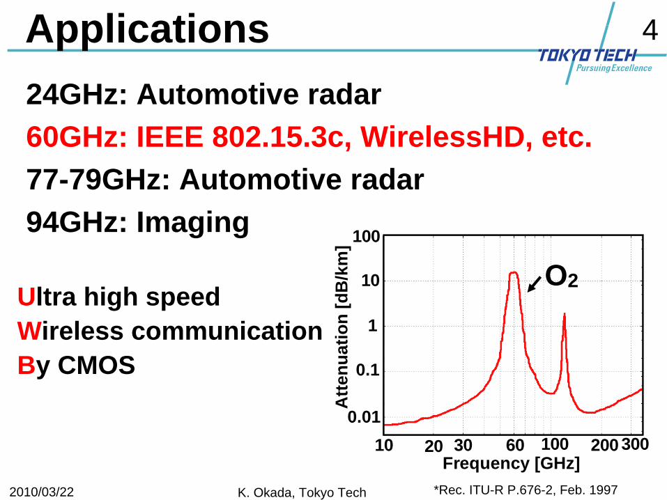
Applications24GHz: Automotive radar60GHz: IEEE 802.15.3c, WirelessHD, etc.77-79GHz: Automotive radar94GHz: Imaging
Ultra high speedWireless communicationBy CMOS
O2
*Rec. ITU-R P.676-2, Feb. 1997
2010/03/22 K. Okada, Tokyo Tech
5
Matsuzawa& Okada Lab.
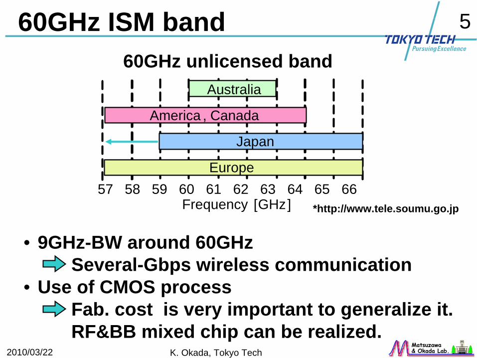
60GHz ISM band60GHz unlicensed band
*http://www.tele.soumu.go.jp
Frequency [GHz]57 58 59 60 61 62 63 64 65 66
America , Canada
Europe
Japan
Australia
Frequency [GHz]57 58 59 60 61 62 63 64 65 66
America , Canada
Europe
Japan
Australia
• 9GHz-BW around 60GHzSeveral-Gbps wireless communication
• Use of CMOS processFab. cost is very important to generalize it.RF&BB mixed chip can be realized.
2010/03/22 K. Okada, Tokyo Tech
6
Matsuzawa& Okada Lab.
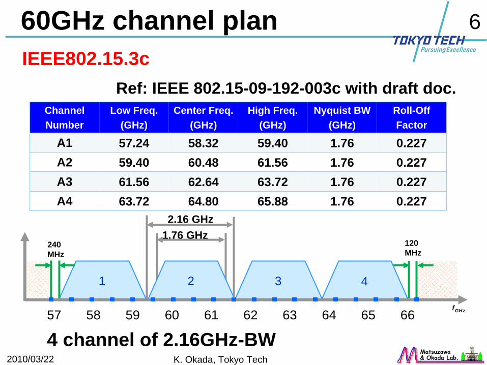
60GHz channel plan
57 58 59 60 61 62 63 64 65 66
IEEE802.15.3c
4 channel of 2.16GHz-BW
Channel Number
Low Freq.(GHz)
Center Freq.(GHz)
High Freq.(GHz)
Nyquist BW(GHz)
Roll-OffFactor
A1 57.24 58.32 59.40 1.76 0.227A2 59.40 60.48 61.56 1.76 0.227A3 61.56 62.64 63.72 1.76 0.227A4 63.72 64.80 65.88 1.76 0.227
1 2 4
240 MHz
120 MHz
1.76 GHz2.16 GHz
3
fGHz
Ref: IEEE 802.15-09-192-003c with draft doc.

2010/03/22 K. Okada, Tokyo Tech
7
Matsuzawa& Okada Lab.
Overview on TG3c System Design • One unified MAC• Three PHYs optimized for respective and specific
market segments– Single carrier (SC) PHY
• low complexity, low power consumption and low cost • handheld mobile applications
– High speed interface (HSI) PHY - OFDM• low latency bi-directional data communications• PC peripherals
– AV PHY - OFDM• optimized for high speed uncompressed video transmission• Audio/visual consumer electronics (CE) applications
Ref: IEEE 802.15-09-192-003c
e.g., 3Gbps(QPSK), 6Gbps(16QAM), 9Gbps(64QAM)x4ch
2010/03/22 K. Okada, Tokyo Tech
8
Matsuzawa& Okada Lab.
Outline
• Motivation• Issues for mmW CMOS Circuits• Device Characterization• De-embedding• Conclusion
2010/03/22 K. Okada, Tokyo Tech
9
Matsuzawa& Okada Lab.
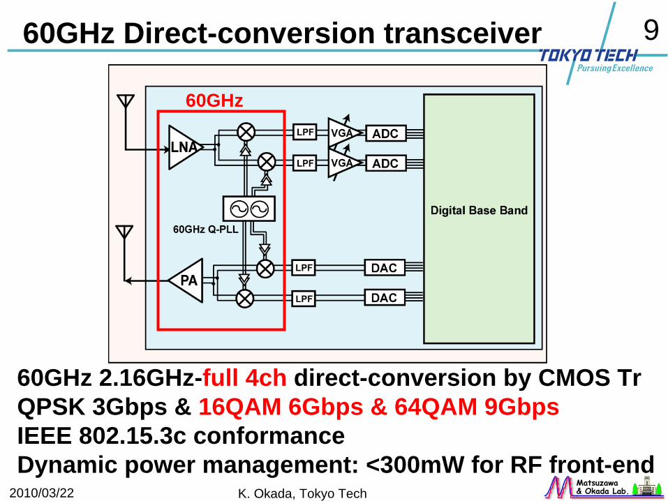
Digital Base Band60GHz Q-PLL
LPF ADC
VGA ADCLNA
VGA
LPF
LPF DAC
DACPA
LPF
60GHz Direct-conversion transceiver
60GHz 2.16GHz-full 4ch direct-conversion by CMOS TrQPSK 3Gbps & 16QAM 6Gbps & 64QAM 9GbpsIEEE 802.15.3c conformanceDynamic power management: <300mW for RF front-end
60GHz

2010/03/22 K. Okada, Tokyo Tech
10
Matsuzawa& Okada Lab.
Circuit blocks of 60GHz transceiver
60GHz LNA
60GHz PA
Down-Mixer
Up-Mixer
20GHz PLL
I/Q TriplerFUJITSU(Eshuttle) CMOS 65nm
2010/03/22 K. Okada, Tokyo Tech
11
Matsuzawa& Okada Lab.
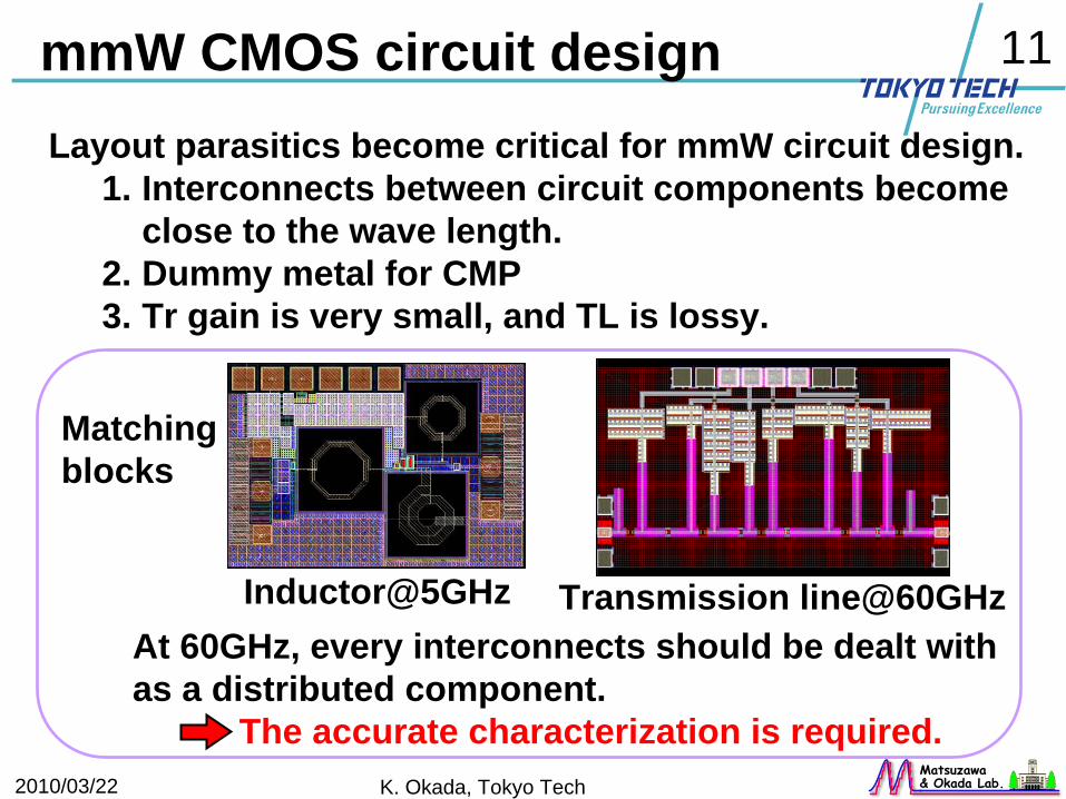
mmW CMOS circuit design
Inductor@5GHz Transmission line@60GHz
Matchingblocks
At 60GHz, every interconnects should be dealt with as a distributed component.
The accurate characterization is required.
Layout parasitics become critical for mmW circuit design.1. Interconnects between circuit components become
close to the wave length.2. Dummy metal for CMP3. Tr gain is very small, and TL is lossy.
2010/03/22 K. Okada, Tokyo Tech
12
Matsuzawa& Okada Lab.
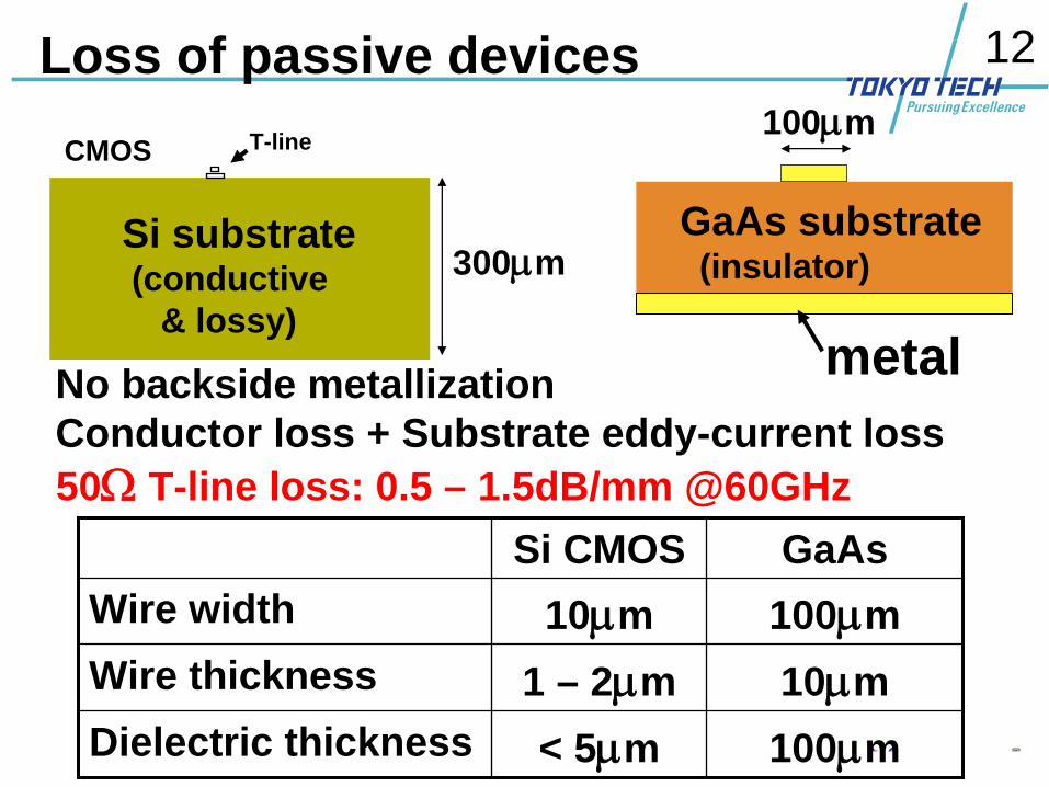
Loss of passive devices
GaAs substrate(insulator)
Si substrate(conductive
& lossy)
100μm
300μm
metal
CMOS T-line
No backside metallizationConductor loss + Substrate eddy-current loss50Ω
T-line loss: 0.5 – 1.5dB/mm @60GHz
Si CMOS GaAsWire width 10μm 100μmWire thickness 1 – 2μm 10μmDielectric thickness < 5μm 100μm
2010/03/22 K. Okada, Tokyo Tech
13
Matsuzawa& Okada Lab.
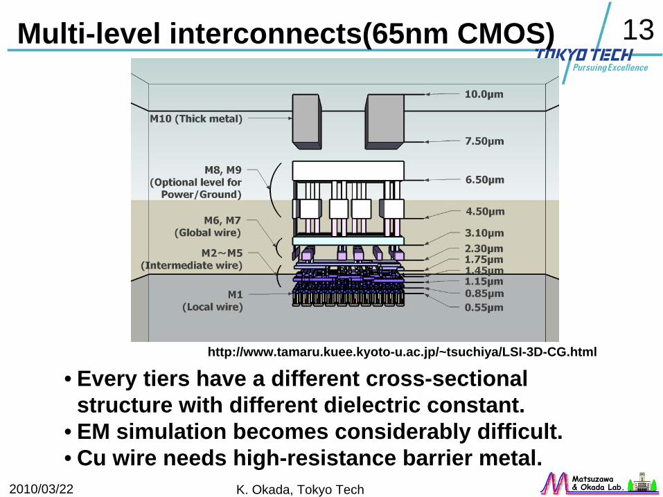
Multi-level interconnects(65nm CMOS)
http://www.tamaru.kuee.kyoto-u.ac.jp/~tsuchiya/LSI-3D-CG.html
• Every tiers have a different cross-sectional structure with different dielectric constant.
• EM simulation becomes considerably difficult.• Cu wire needs high-resistance barrier metal.
2010/03/22 K. Okada, Tokyo Tech
14
Matsuzawa& Okada Lab.
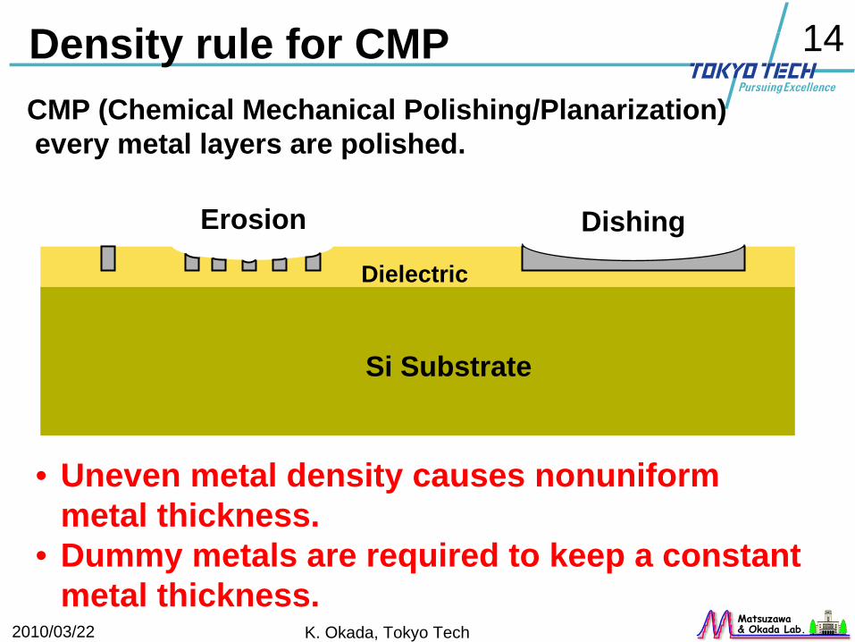
Density rule for CMP
Si Substrate
Dielectric
CMP (Chemical Mechanical Polishing/Planarization)every metal layers are polished.
DishingErosion
• Uneven metal density causes nonuniform metal thickness.
• Dummy metals are required to keep a constant metal thickness.
2010/03/22 K. Okada, Tokyo Tech
15
Matsuzawa& Okada Lab.
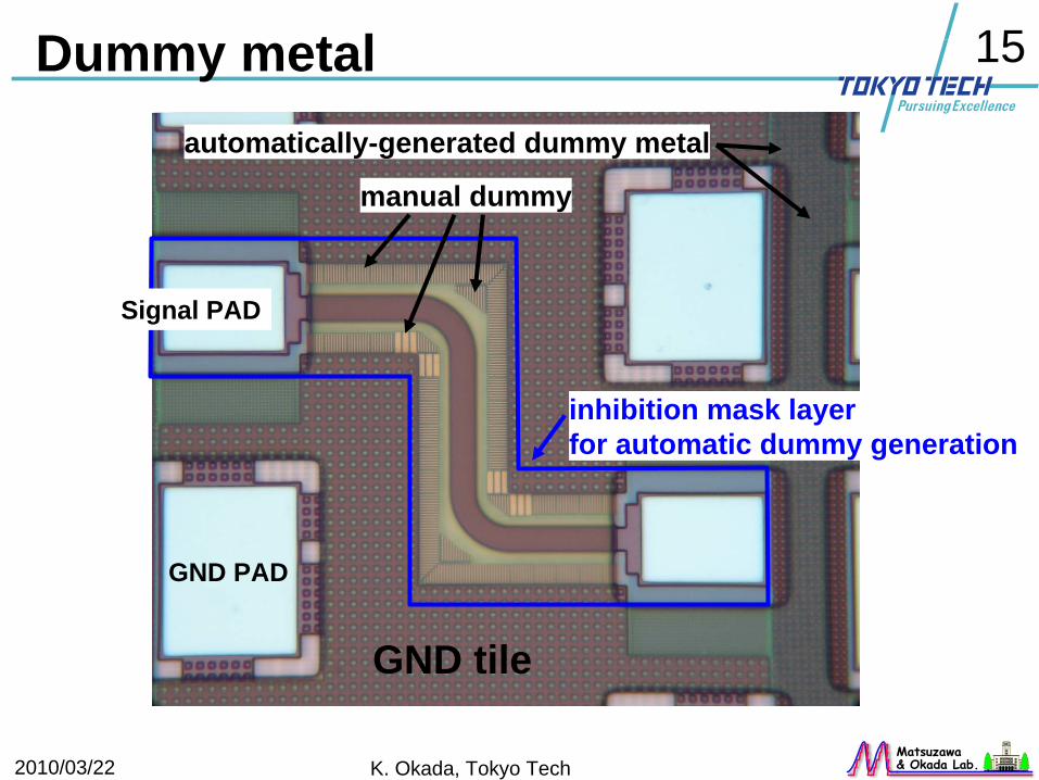
Dummy metal
GND PAD
automatically-generated dummy metal
GND tile
manual dummy
Signal PAD
inhibition mask layerfor automatic dummy generation
2010/03/22 K. Okada, Tokyo Tech
16
Matsuzawa& Okada Lab.
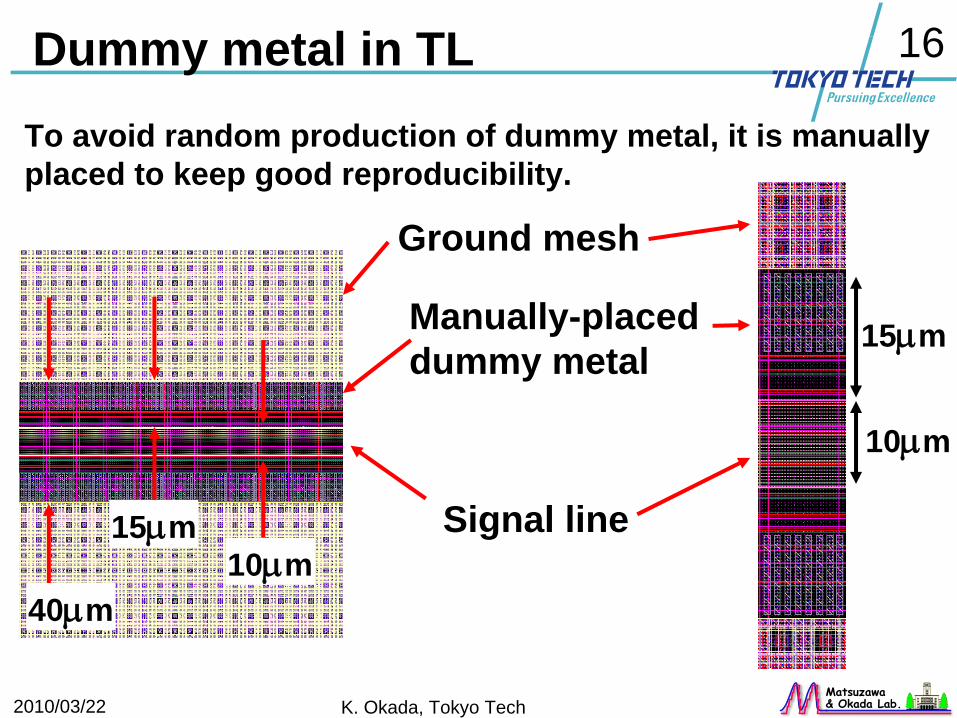
Dummy metal in TL
Metal dummy
To avoid random production of dummy metal, it is manuallyplaced to keep good reproducibility.
Ground mesh
Manually-placeddummy metal
Signal line10μm
15μm
40μm
10μm
15μm
2010/03/22 K. Okada, Tokyo Tech
17
Matsuzawa& Okada Lab.
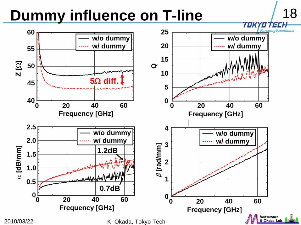
Dummy influence on T-linew/o dummyw/ dummy
0
400
100
300200
500600
0 20 6040Frequency [GHz]
L [p
H/m
m]
0 20 6040
200
50
150
100
250
0
Frequency [GHz]
w/o dummyw/ dummy
C [f
F/m
m]
3
2
1
4
0
G [m
S/m
m]
0 20 6040Frequency [GHz]
w/o dummyw/ dummy
0 20 6040Frequency [GHz]
15
10
5
20
0
w/o dummyw/ dummy
2010/03/22 K. Okada, Tokyo Tech
18
Matsuzawa& Okada Lab.
Dummy influence on T-line
0 20 6040Frequency [GHz]
w/o dummyw/ dummy55
50
45
60
400 20 6040
Frequency [GHz]
20
5
15
10
25
0
Q
w/o dummyw/ dummy
0 20 6040Frequency [GHz]
2.0
0.5
1.5
1.0
2.5
0
w/o dummyw/ dummy
0 20 6040Frequency [GHz]
3
2
1
4
0
w/o dummyw/ dummy
[×103]
5Ω
diff.
0.7dB
1.2dBβ
[rad
/mm
]
2010/03/22 K. Okada, Tokyo Tech
19
Matsuzawa& Okada Lab.
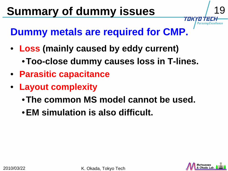
Summary of dummy issues
• Loss (mainly caused by eddy current)• Too-close dummy causes loss in T-lines.
• Parasitic capacitance• Layout complexity
• The common MS model cannot be used.• EM simulation is also difficult.
Dummy metals are required for CMP.
2010/03/22 K. Okada, Tokyo Tech
20
Matsuzawa& Okada Lab.
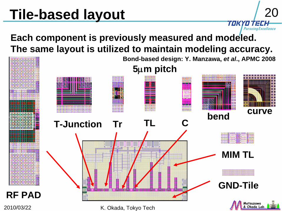
Tile-based layout
T-Junction Tr TL C
GND-TileRF PAD
Each component is previously measured and modeled.The same layout is utilized to maintain modeling accuracy.
MIM TL
5μm pitch
curvebend
Bond-based design: Y. Manzawa, et al., APMC 2008
2010/03/22 K. Okada, Tokyo Tech
21
Matsuzawa& Okada Lab.
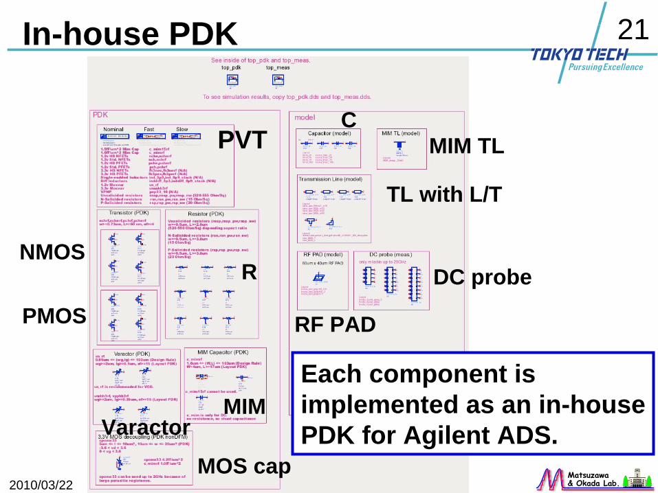
In-house PDK
Each component isimplemented as an in-housePDK for Agilent ADS.
PVT
RNMOS
MOS cap
VaractorMIM
DC probe
RF PAD
MIM TL
TL with L/T
C
PMOS
2010/03/22 K. Okada, Tokyo Tech
22
Matsuzawa& Okada Lab.
Remaining issues
• Tile-based layout• Layout and circuit model are strictly corresponded,
which contributes to avoid uncertainty caused by dummy metals and interconnections between circuit components.
• Measurement• mmW measurement is still challenging• Accuracy of de-embedding becomes a considerably
sensitive at mmW frequencies.• Characterization
• No fab-provided PDK for mmW circuit design• Measurement is not so accurate• TEG is very important.
2010/03/22 K. Okada, Tokyo Tech
23
Matsuzawa& Okada Lab.
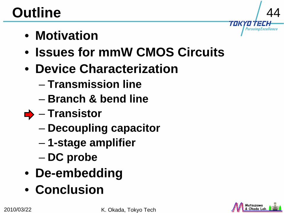
Outline• Motivation• Issues for mmW CMOS Circuits• Device Characterization
– Transmission line – Branch & bend line– Transistor– Decoupling capacitor– 1-stage amplifier– DC probe
• De-embedding• Conclusion
2010/03/22 K. Okada, Tokyo Tech
24
Matsuzawa& Okada Lab.
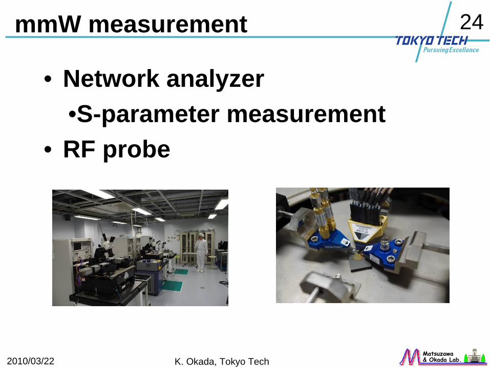
mmW measurement
• Network analyzer•S-parameter measurement
• RF probe
2010/03/22 K. Okada, Tokyo Tech
25
Matsuzawa& Okada Lab.
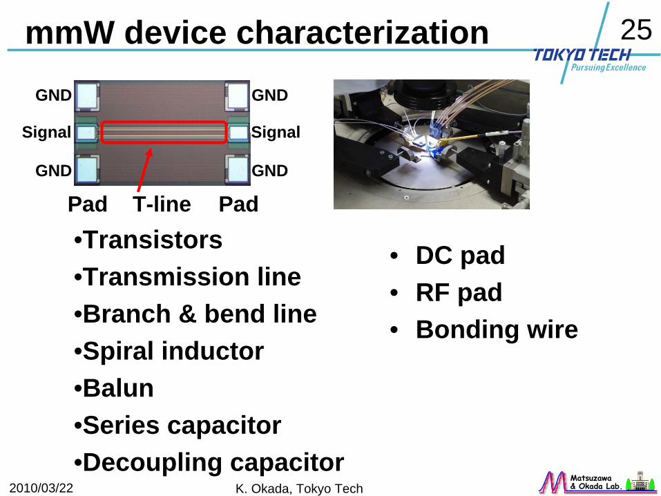
mmW device characterization
•Transistors•Transmission line•Branch & bend line•Spiral inductor•Balun•Series capacitor•Decoupling capacitor
Pad T-line Pad
• DC pad• RF pad• Bonding wire
GND
GND
GND
GND
Signal Signal
2010/03/22 K. Okada, Tokyo Tech
26
Matsuzawa& Okada Lab.
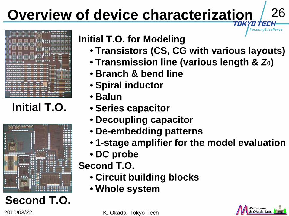
Overview of device characterization
Initial T.O.
Second T.O.
Initial T.O. for Modeling• Transistors (CS, CG with various layouts)• Transmission line (various length & Z0)• Branch & bend line• Spiral inductor• Balun• Series capacitor• Decoupling capacitor• De-embedding patterns• 1-stage amplifier for the model evaluation• DC probe
Second T.O.• Circuit building blocks• Whole system
2010/03/22 K. Okada, Tokyo Tech
27
Matsuzawa& Okada Lab.
Outline• Motivation• Issues for mmW CMOS Circuits• Device Characterization
– Transmission line – Branch & bend line– Transistor– Decoupling capacitor– 1-stage amplifier– DC probe
• De-embedding• Conclusion
2010/03/22 K. Okada, Tokyo Tech
28
Matsuzawa& Okada Lab.
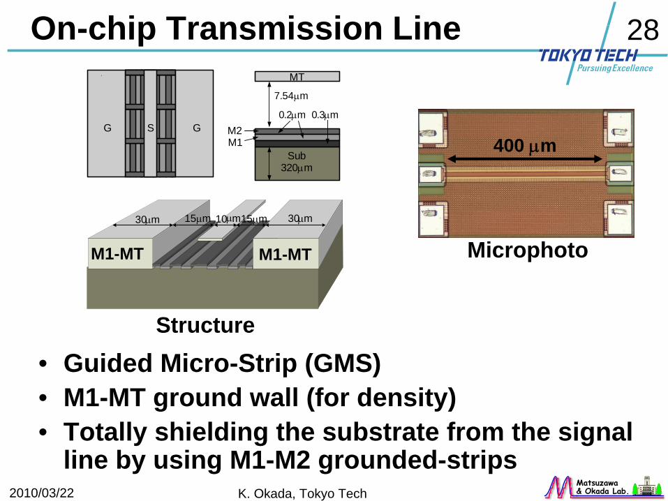
On-chip Transmission Line
• Guided Micro-Strip (GMS)• M1-MT ground wall (for density)• Totally shielding the substrate from the signal
line by using M1-M2 grounded-strips
Structure
400 μm
Microphoto
320μm
7.54μm
0.2μm 0.3μmGSG
MT
SubM1M2
15 mμ 10 m 30μmμ30μm 15 mμ
M1-MTM1-MT
2010/03/22 K. Okada, Tokyo Tech
29
Matsuzawa& Okada Lab.
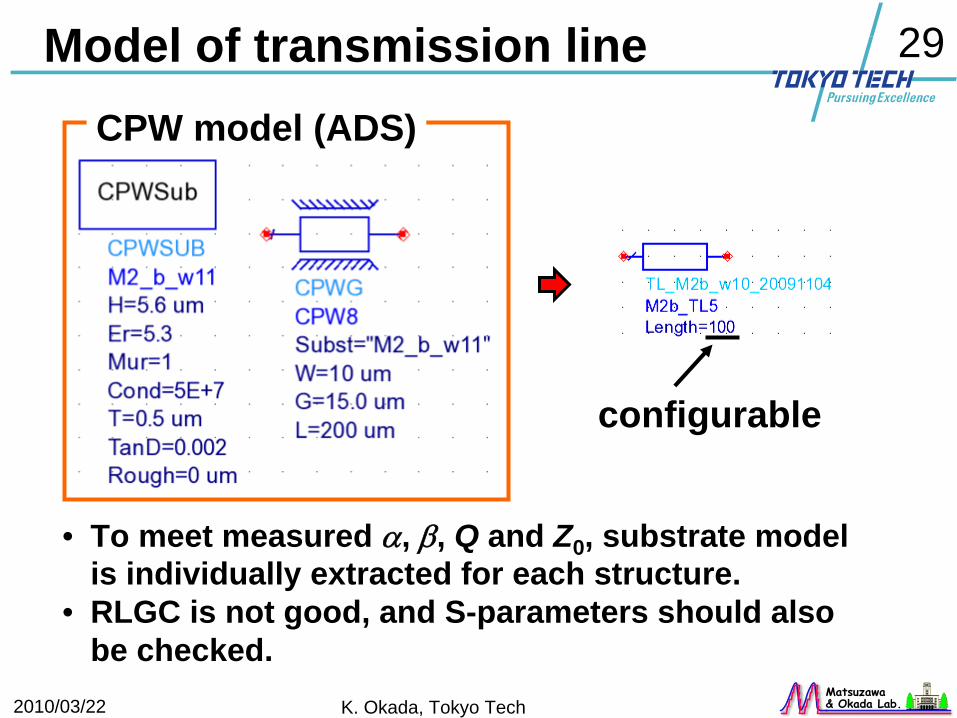
Model of transmission lineCPW model (ADS)
• To meet measured α, β, Q and Z0 , substrate model is individually extracted for each structure.
• RLGC is not good, and S-parameters should also be checked.
configurable
2010/03/22 K. Okada, Tokyo Tech
30
Matsuzawa& Okada Lab.
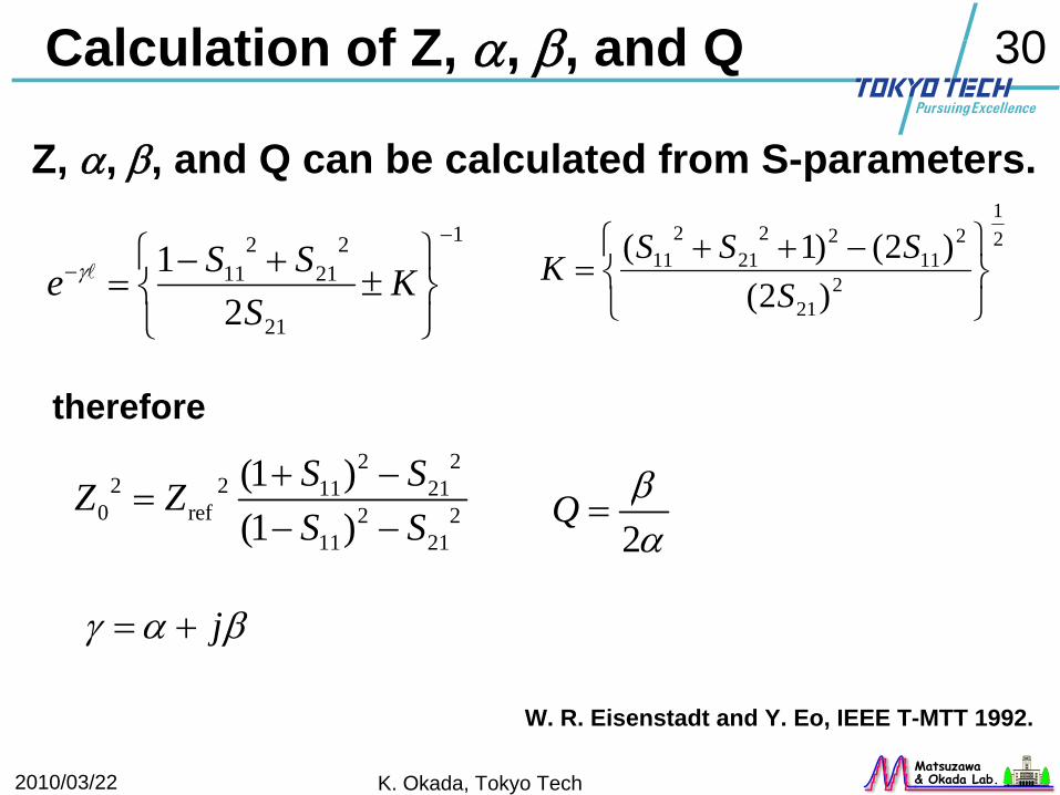
Calculation of Z, α, β, and Q
2 22 2 11 21
0 ref 2 211 21
(1 )(1 )
S SZ ZS S
+ −=
− −
1
21
221
211
21
−
−
⎭⎬⎫
⎩⎨⎧
±+−
= KS
SSe lγ21
221
211
2221
211
)2()2()1(
⎭⎬⎫
⎩⎨⎧ −++
=S
SSSK
2Q β
α=
Z, α, β, and Q can be calculated from S-parameters.
therefore
jγ α β= +
W. R. Eisenstadt and Y. Eo, IEEE T-MTT 1992.
2010/03/22 K. Okada, Tokyo Tech
31
Matsuzawa& Okada Lab.
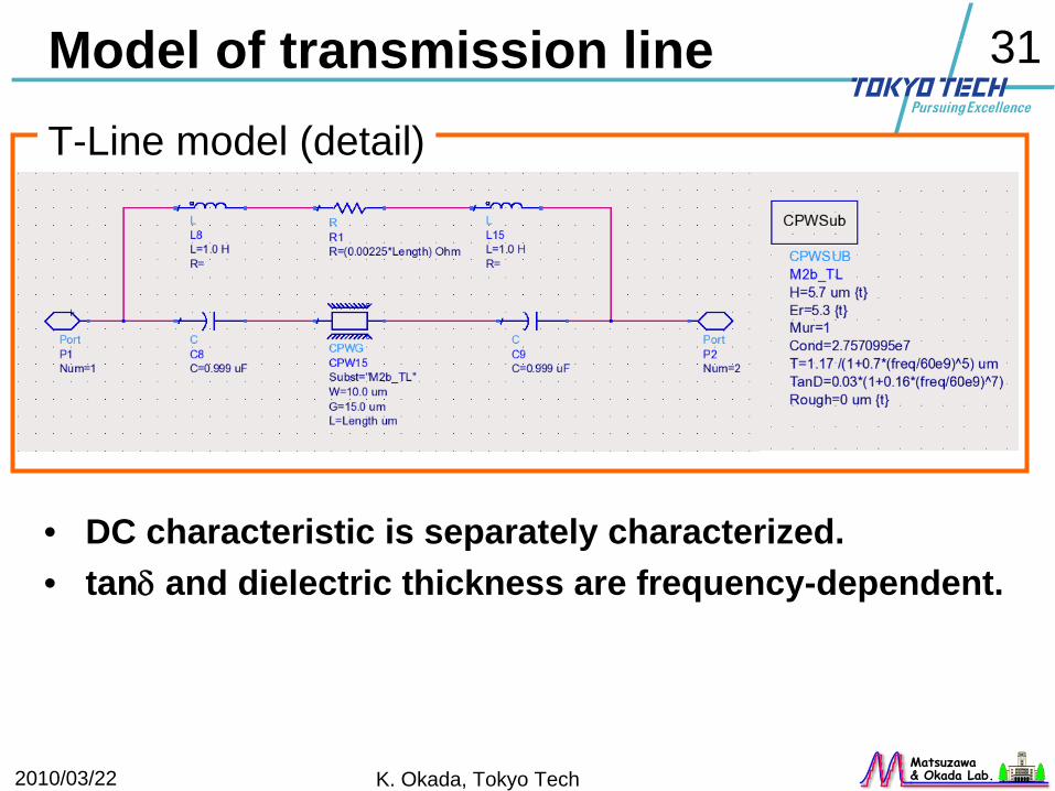
Model of transmission lineT-Line model (detail)
• DC characteristic is separately characterized.• tanδ
and dielectric thickness are frequency-dependent.

2010/03/22 K. Okada, Tokyo Tech
32
Matsuzawa& Okada Lab.
Transmission line (400μm)
Characteristic impedance
Quality factor
Attenuation constant
Phase constant
2010/03/22 K. Okada, Tokyo Tech
33
Matsuzawa& Okada Lab.
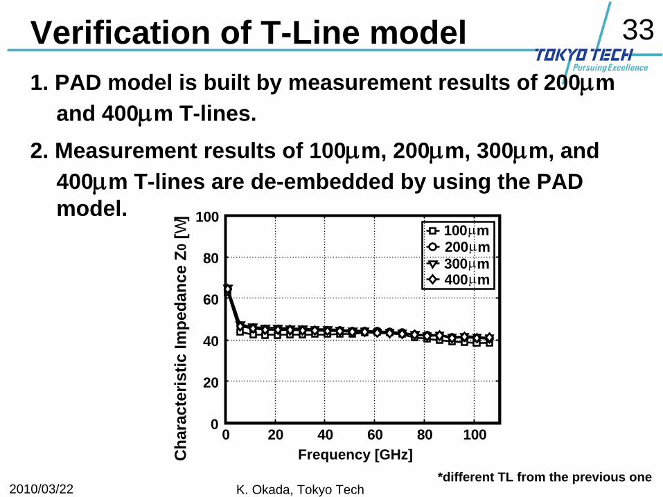
Verification of T-Line model1. PAD model is built by measurement results of 200μm
and 400μm T-lines.2. Measurement results of 100μm, 200μm, 300μm, and
400μm T-lines are de-embedded by using the PAD model.
*different TL from the previous one
0 20 40 60 80 1000
20
40
60
80
100
200μm100μm
300μm400μm
Frequency [GHz]Cha
ract
eris
tic Im
peda
nce
Z0 [W
]

2010/03/22 K. Okada, Tokyo Tech
34
Matsuzawa& Okada Lab.
Outline• Motivation• Issues for mmW CMOS Circuits• Device Characterization
– Transmission line – Branch & bend line– Transistor– Decoupling capacitor– 1-stage amplifier– DC probe
• De-embedding• Conclusion
2010/03/22 K. Okada, Tokyo Tech
35
Matsuzawa& Okada Lab.
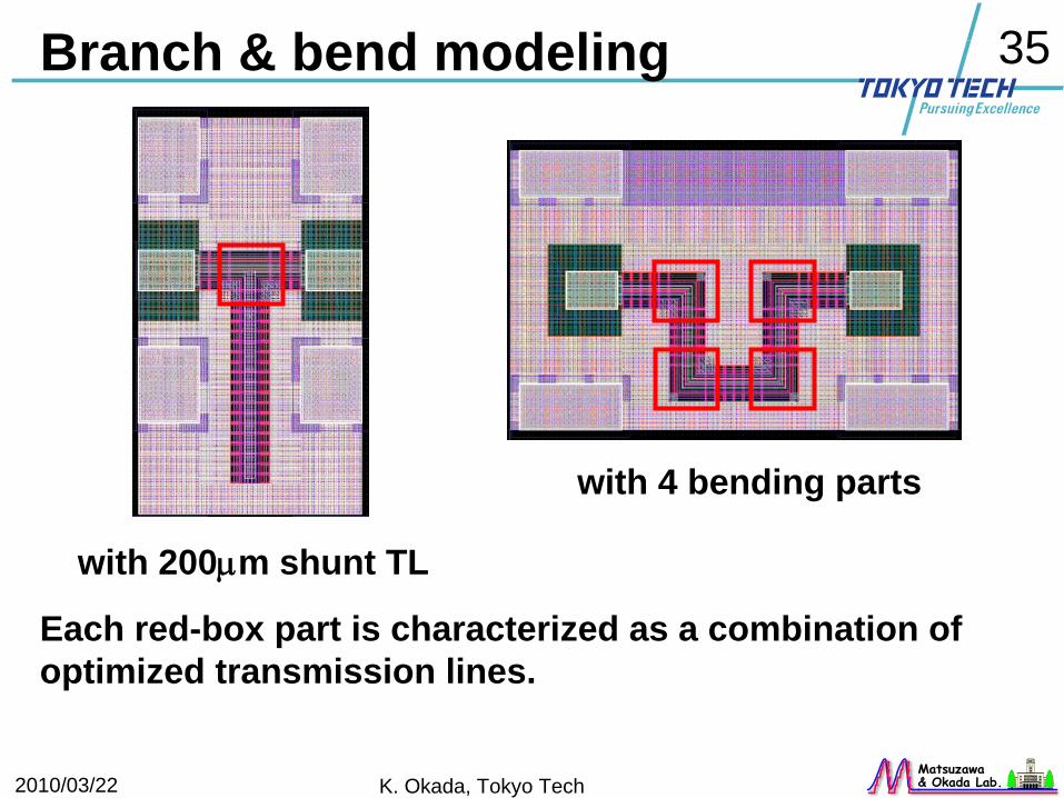
Branch & bend modeling
with 4 bending parts
with 200μm shunt TL
Each red-box part is characterized as a combination of optimized transmission lines.
2010/03/22 K. Okada, Tokyo Tech
36
Matsuzawa& Okada Lab.
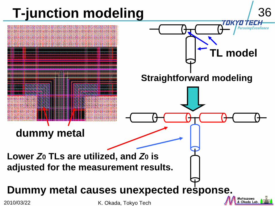
T-junction modeling
Straightforward modeling
Lower Z0 TLs are utilized, and Z0 isadjusted for the measurement results.
Dummy metal causes unexpected response.
TL model
dummy metal
2010/03/22 K. Okada, Tokyo Tech
37
Matsuzawa& Okada Lab.
-1.0
-0.8
-0.6
-0.4
-0.2
0
0 20 40 60
MeasurementWithout T modelWith T modelModeling
Frequency [GHz]
S21
[dB
]
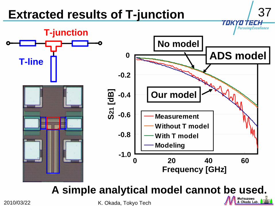
Extracted results of T-junction
ADS model
Our model
No model
A simple analytical model cannot be used.
T-junction
T-line
2010/03/22 K. Okada, Tokyo Tech
38
Matsuzawa& Okada Lab.
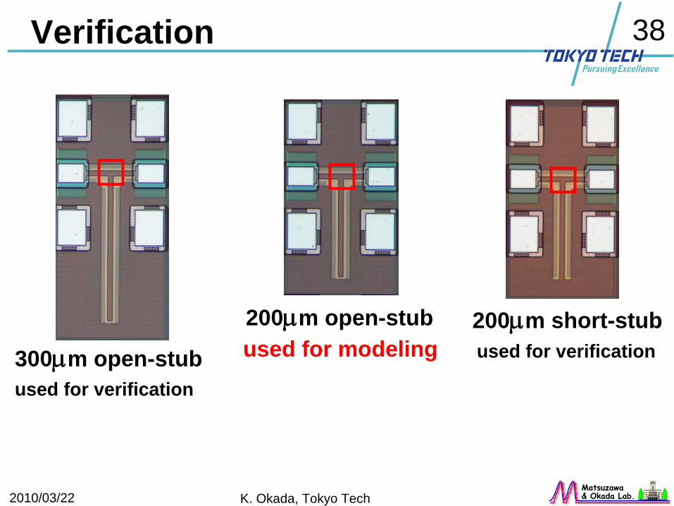
Verification
300μm open-stub
200μm open-stub 200μm short-stubused for modeling
used for verification
used for verification
2010/03/22 K. Okada, Tokyo Tech
39
Matsuzawa& Okada Lab.
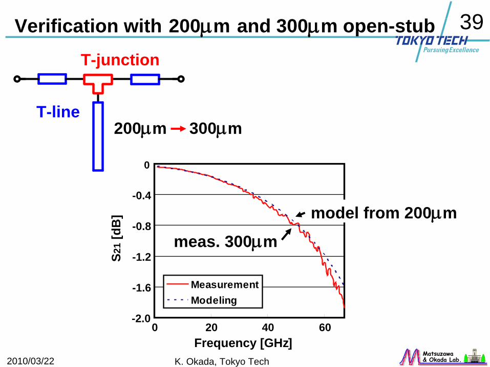
Verification with 200μm and 300μm open-stub
-2.0
-1.6
-1.2
-0.8
-0.4
0
0 20 40 60Frequency [GHz]
S21
[dB
]
ModelingMeasurement
200μm 300μm
model from 200μm
meas. 300μm
T-junction
T-line
2010/03/22 K. Okada, Tokyo Tech
40
Matsuzawa& Okada Lab.
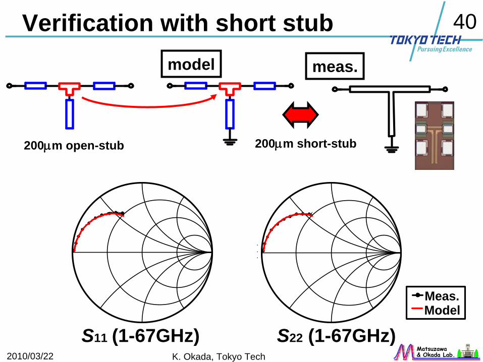
Verification with short stub
S11 (1-67GHz) S22 (1-67GHz)
Meas.Model
model meas.
200μm open-stub 200μm short-stub
2010/03/22 K. Okada, Tokyo Tech
41
Matsuzawa& Okada Lab.
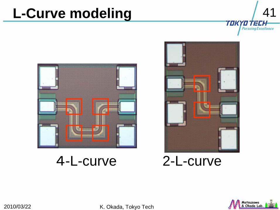
L-Curve modeling
4-L-curve 2-L-curve
2010/03/22 K. Okada, Tokyo Tech
42
Matsuzawa& Okada Lab.
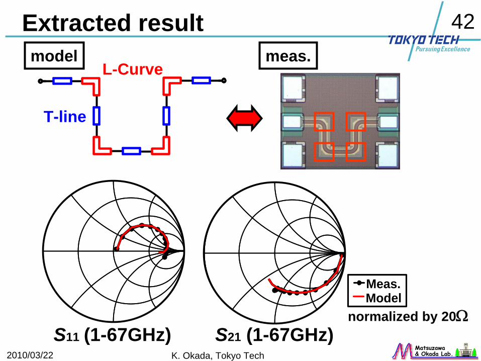
Extracted result
S11 (1-67GHz) S21 (1-67GHz)
Meas.Model
L-Curve
T-line
model meas.
normalized by 20Ω
2010/03/22 K. Okada, Tokyo Tech
43
Matsuzawa& Okada Lab.
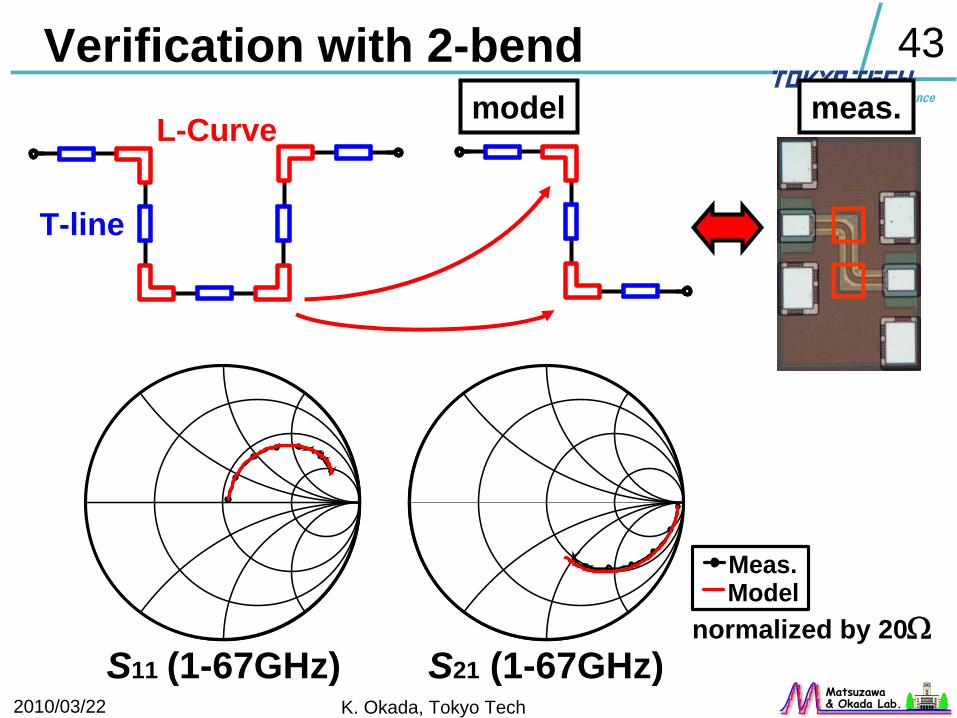
Verification with 2-bendL-Curve
T-line
model meas.
S11 (1-67GHz) S21 (1-67GHz)
Meas.Model
normalized by 20Ω
2010/03/22 K. Okada, Tokyo Tech
44
Matsuzawa& Okada Lab.
Outline• Motivation• Issues for mmW CMOS Circuits• Device Characterization
– Transmission line – Branch & bend line– Transistor– Decoupling capacitor– 1-stage amplifier– DC probe
• De-embedding• Conclusion
2010/03/22 K. Okada, Tokyo Tech
45
Matsuzawa& Okada Lab.
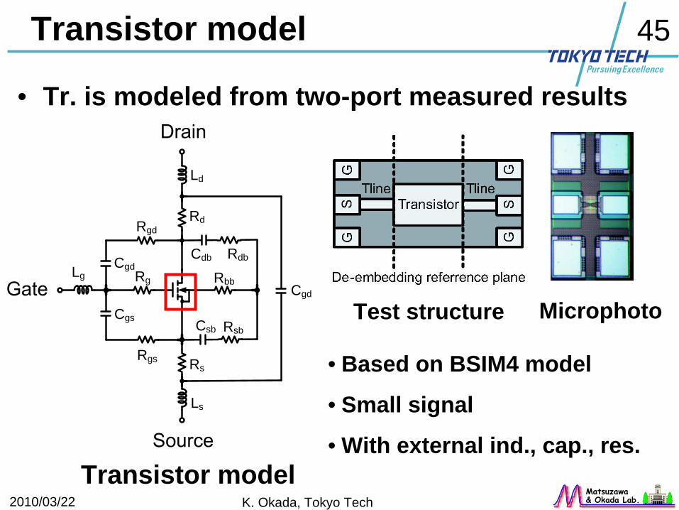
Transistor model
Cgd
Rd
Rs
Cgs
Rgd
Rgs
Lg Rg
Cdb Rdb
RsbCsb
RbbCgd
Ls
Ld
Transistor model
• Based on BSIM4 model
• Small signal
• With external ind., cap., res.
MicrophotoTest structure
• Tr. is modeled from two-port measured results
2010/03/22 K. Okada, Tokyo Tech
46
Matsuzawa& Okada Lab.
Extracted results of Tr model
0 20 40 60 80 100-1
-0.5
0
0.5
1
Frequency [GHz]
Meas.Model
Re[S11]
Im[S11]
S11
S11
0 20 40 60 80 100-0.1
0.0
0.1
0.2
0.3
S12
Frequency [GHz]
Meas.Model
Im[S12]
Re[S12]
S12
0 20 40 60 80 100-4
-2
0
2
4
Frequency [GHz]
Meas.Model
S21
Re[S21]
Im[S21]
S21
0 20 40 60 80 100-1
-0.5
0
0.5
1
Frequency [GHz]
Meas.Model
Im[S22]
Re[S22]S2
2
S22
2010/03/22 K. Okada, Tokyo Tech
47
Matsuzawa& Okada Lab.
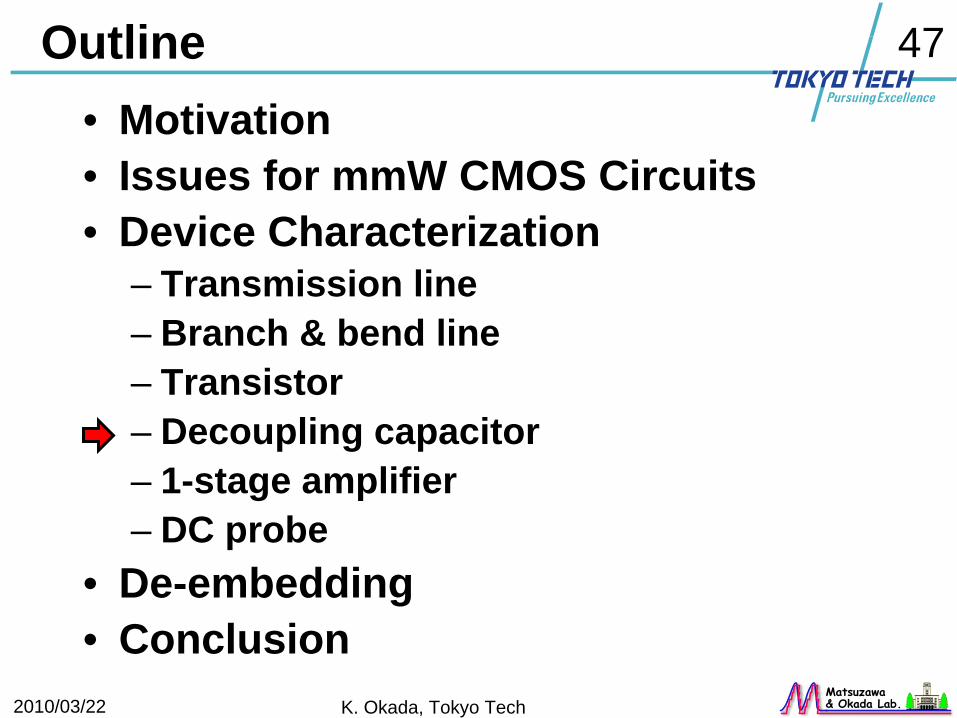
Outline• Motivation• Issues for mmW CMOS Circuits• Device Characterization
– Transmission line – Branch & bend line– Transistor– Decoupling capacitor– 1-stage amplifier– DC probe
• De-embedding• Conclusion
2010/03/22 K. Okada, Tokyo Tech
48
Matsuzawa& Okada Lab.
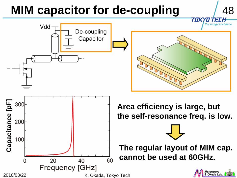
MIM capacitor for de-coupling
Area efficiency is large, butthe self-resonance freq. is low.
The regular layout of MIM cap.cannot be used at 60GHz.
Cap
acita
nce
[pF]
2010/03/22 K. Okada, Tokyo Tech
49
Matsuzawa& Okada Lab.
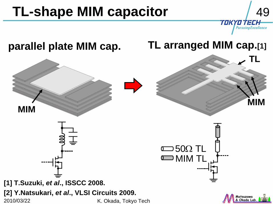
TL-shape MIM capacitor
50Ω TLMIM TL
parallel plate MIM cap. TL arranged MIM cap.[1]
TL
MIMMIM
[1] T.Suzuki, et al., ISSCC 2008.[2] Y.Natsukari, et al., VLSI Circuits 2009.
2010/03/22 K. Okada, Tokyo Tech
50
Matsuzawa& Okada Lab.
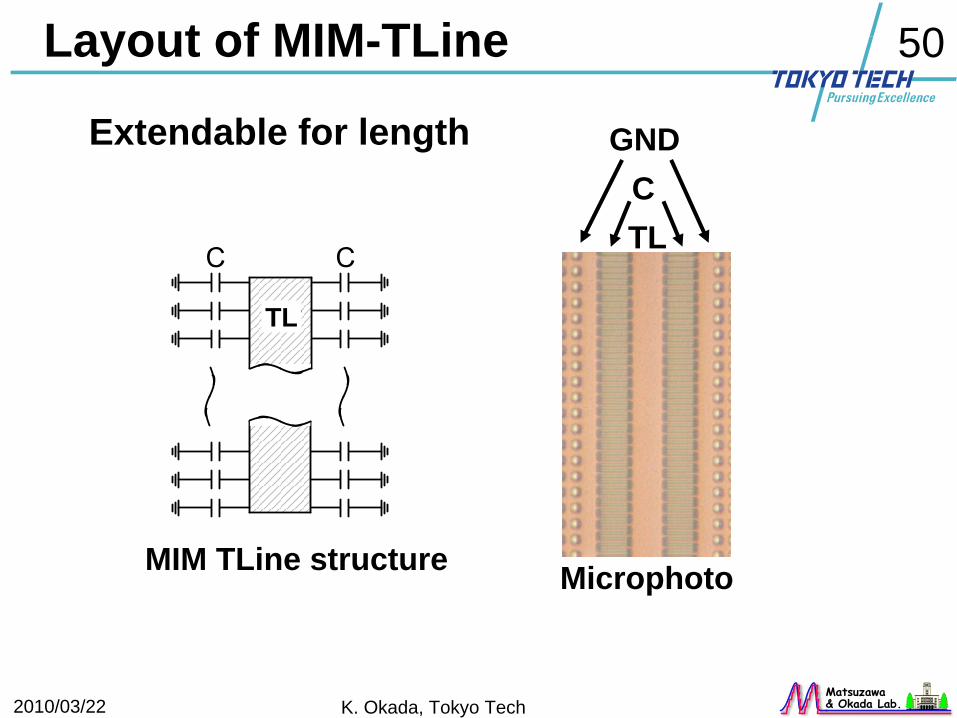
Layout of MIM-TLine
MIM TLine structure
Extendable for length
Microphoto
TL
CTL
GND
2010/03/22 K. Okada, Tokyo Tech
51
Matsuzawa& Okada Lab.
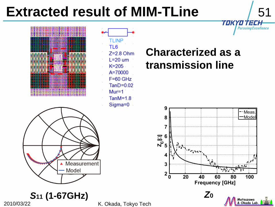
Extracted result of MIM-TLine
S11 (1-67GHz) Z0
Characterized as atransmission line
2010/03/22 K. Okada, Tokyo Tech
52
Matsuzawa& Okada Lab.
Outline• Motivation• Issues for mmW CMOS Circuits• Device Characterization
– Transmission line – Branch & bend line– Transistor– Decoupling capacitor– 1-stage amplifier– DC probe
• De-embedding• Conclusion
2010/03/22 K. Okada, Tokyo Tech
53
Matsuzawa& Okada Lab.
An evaluation using a 1-stage amplifier
Schematic
210μm100fF
340μm
RFin
De-coupling MIM T-Line
W=40μm
20μm 100fF
90μm10μm
210μm
RFout
150μm
A 1-stage amplifier is also used for a verification.
2010/03/22 K. Okada, Tokyo Tech
54
Matsuzawa& Okada Lab.
Simulation vs Measurement
S11(gate-side reflection) S22(drain-side reflection)
Meas.Model
2010/03/22 K. Okada, Tokyo Tech
55
Matsuzawa& Okada Lab.
Simulation vs Measurement
Meas.Model
50 60 70 80 90-4
-2
0
2
4
6Po
wer
Gai
n[d
B]
Frequency [GHz]
Meas.Sim.
2010/03/22 K. Okada, Tokyo Tech
56
Matsuzawa& Okada Lab.
Outline• Motivation• Issues for mmW CMOS Circuits• Device Characterization
– Transmission line – Branch & bend line– Transistor– Decoupling capacitor– 1-stage amplifier– DC probe
• De-embedding• Conclusion
2010/03/22 K. Okada, Tokyo Tech
57
Matsuzawa& Okada Lab.
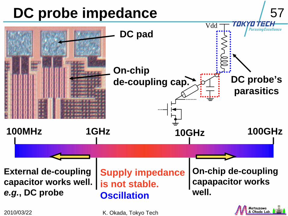
DC probe impedance
100MHz 1GHz 10GHz 100GHz
External de-couplingcapacitor works well.e.g., DC probe
On-chip de-coupling capapacitor works well.
Supply impedanceis not stable.Oscillation
Vdd
On-chipde-coupling cap. DC probe’s
parasitics
DC pad
2010/03/22 K. Okada, Tokyo Tech
58
Matsuzawa& Okada Lab.
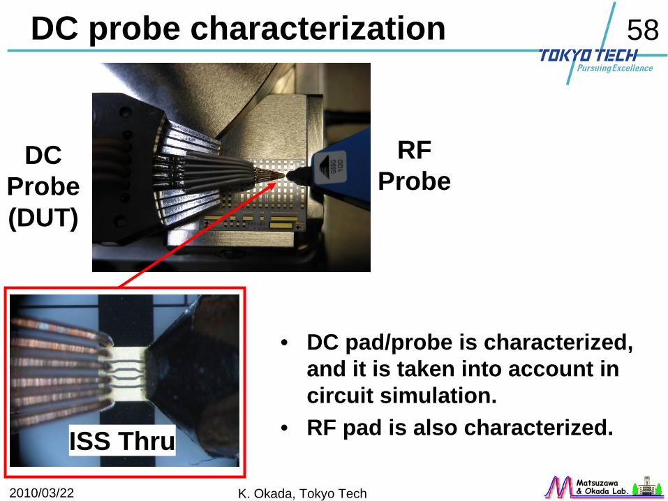
DC probe characterization
RF Probe
DC Probe(DUT)
ISS Thru
• DC pad/probe is characterized, and it is taken into account in circuit simulation.
• RF pad is also characterized.
2010/03/22 K. Okada, Tokyo Tech
59
Matsuzawa& Okada Lab.
Other modeling issues
• De-embedding• Transistor layout optimization• Spiral inductor• Balun• RF Pad• DC probe / bonding wire / bump / filler / PCB
2010/03/22 K. Okada, Tokyo Tech
60
Matsuzawa& Okada Lab.
Summary
1. Design issue of TL on CMOS chips is different from that of compound semiconductors. e.g., dummy metal, lossy substrate, large conductive
loss, etc2. Branch modeling3. Distributed modeling of de-couple MIM cap.4. Evaluation using a 1-stage amplifier
A modeling approach to design a 60GHz CMOS amplifiers
2010/03/22 K. Okada, Tokyo Tech
61
Matsuzawa& Okada Lab.
Outline
• Motivation• Issues for mmW CMOS Circuits• Device Characterization• De-embedding
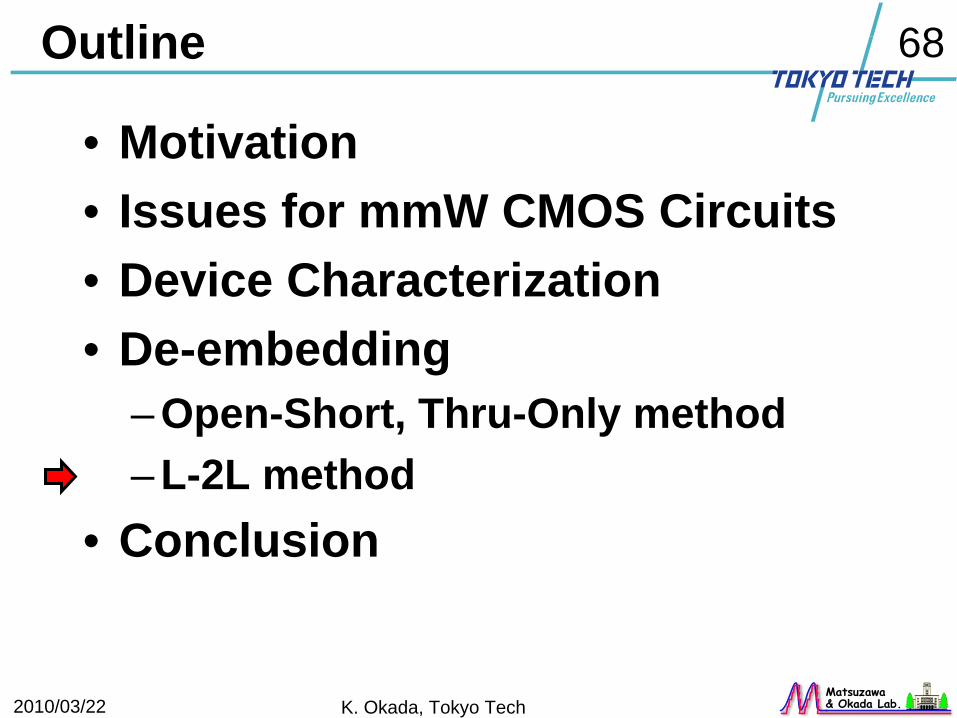
– Open-Short, Thru-Only method– L-2L method
• Conclusion
2010/03/22 K. Okada, Tokyo Tech
62
Matsuzawa& Okada Lab.
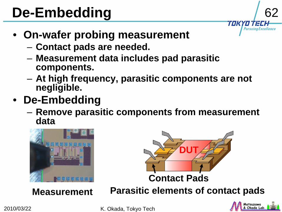
De-Embedding• On-wafer probing measurement
– Contact pads are needed.– Measurement data includes pad parasitic
components.– At high frequency, parasitic components are not
negligible.• De-Embedding
– Remove parasitic components from measurement data
Measurement Parasitic elements of contact pads
DUT
Contact Pads
2010/03/22 K. Okada, Tokyo Tech
63
Matsuzawa& Okada Lab.
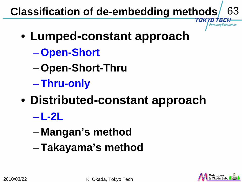
Classification of de-embedding methods
• Lumped-constant approach– Open-Short– Open-Short-Thru– Thru-only
• Distributed-constant approach– L-2L– Mangan’s method– Takayama’s method
2010/03/22 K. Okada, Tokyo Tech
64
Matsuzawa& Okada Lab.
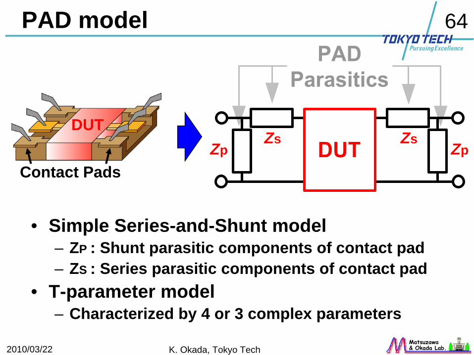
PAD model
ZsZp
ZsZp
DUT
Contact Pads
• Simple Series-and-Shunt model– ZP : Shunt parasitic components of contact pad– ZS : Series parasitic components of contact pad
• T-parameter model– Characterized by 4 or 3 complex parameters
2010/03/22 K. Okada, Tokyo Tech
65
Matsuzawa& Okada Lab.
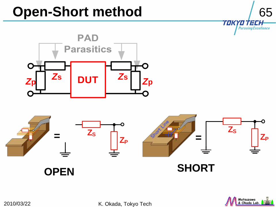
Open-Short method
Zs ZpZsZp
ZPZS
OPEN
ZPZS
SHORT
= =
2010/03/22 K. Okada, Tokyo Tech
66
Matsuzawa& Okada Lab.
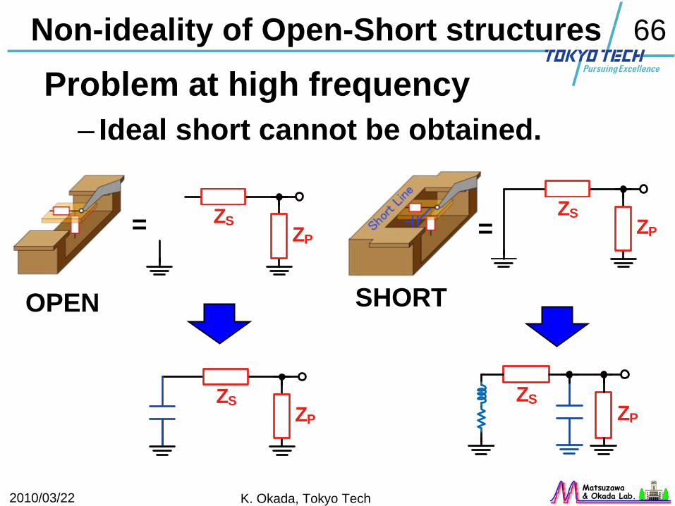
Non-ideality of Open-Short structuresProblem at high frequency
– Ideal short cannot be obtained.
ZPZS
ZPZS
ZPZS
OPEN
ZPZS
SHORT
= =
2010/03/22 K. Okada, Tokyo Tech
67
Matsuzawa& Okada Lab.
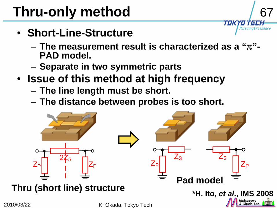
Thru-only method
Thru (short line) structure Pad model
• Short-Line-Structure– The measurement result is characterized as a “π”-
PAD model.– Separate in two symmetric parts
• Issue of this method at high frequency– The line length must be short.– The distance between probes is too short.
*H. Ito, et al., IMS 2008
2010/03/22 K. Okada, Tokyo Tech
68
Matsuzawa& Okada Lab.
Outline
• Motivation• Issues for mmW CMOS Circuits• Device Characterization• De-embedding
– Open-Short, Thru-Only method– L-2L method
• Conclusion
2010/03/22 K. Okada, Tokyo Tech
69
Matsuzawa& Okada Lab.
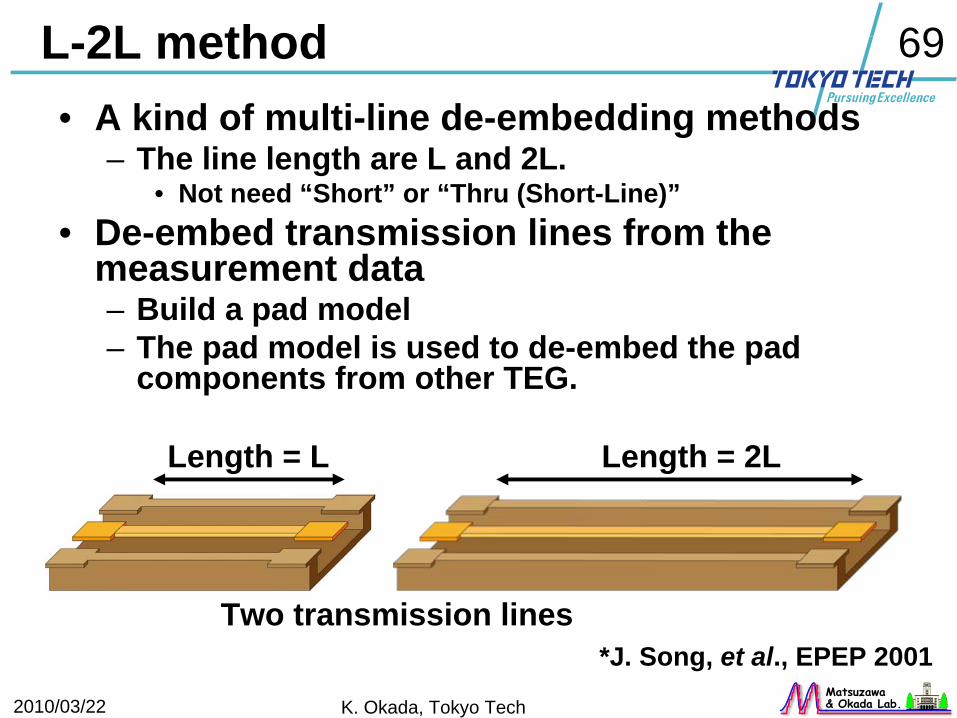
L-2L method• A kind of multi-line de-embedding methods
– The line length are L and 2L.• Not need “Short” or “Thru (Short-Line)”
• De-embed transmission lines from the measurement data– Build a pad model– The pad model is used to de-embed the pad
components from other TEG.
Length = L Length = 2L
Two transmission lines*J. Song, et al., EPEP 2001
2010/03/22 K. Okada, Tokyo Tech
70
Matsuzawa& Okada Lab.
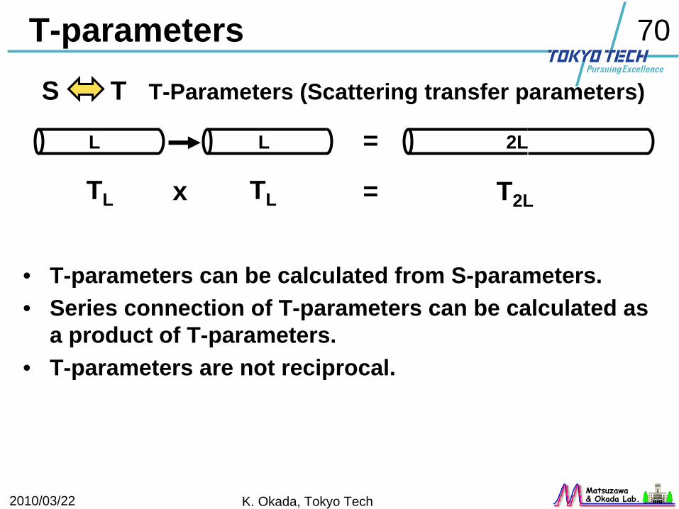
T-parameters
TL T2L
S T
x TL =
=L L 2L
• T-parameters can be calculated from S-parameters.• Series connection of T-parameters can be calculated as
a product of T-parameters.• T-parameters are not reciprocal.
T-Parameters (Scattering transfer parameters)
2010/03/22 K. Okada, Tokyo Tech
71
Matsuzawa& Okada Lab.
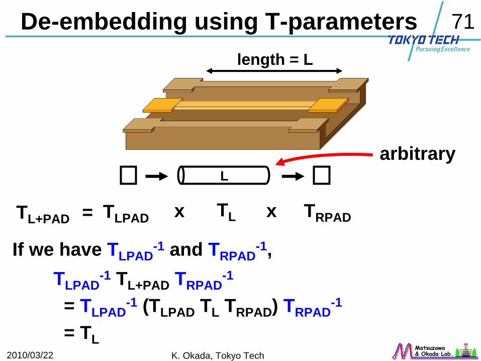
De-embedding using T-parameters
TLPAD TRPAD
length = L
TL x
L
x=TL+PAD
If we have TLPAD-1 and TRPAD
-1,TLPAD
-1 TL+PAD TRPAD-1
= TLPAD-1 (TLPAD TL TRPAD ) TRPAD
-1
= TL
arbitrary
2010/03/22 K. Okada, Tokyo Tech
72
Matsuzawa& Okada Lab.
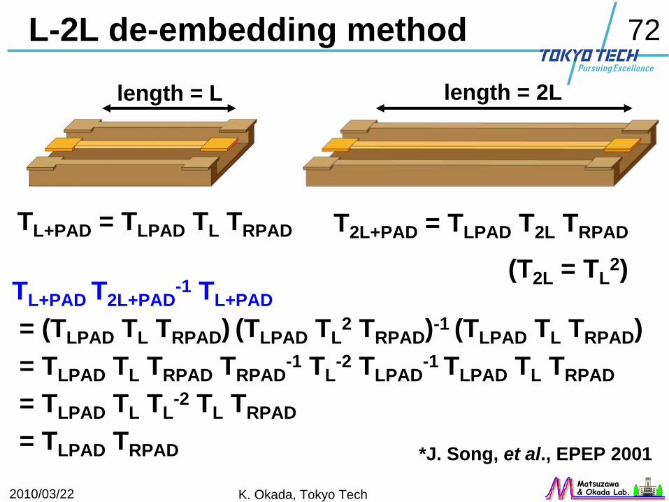
L-2L de-embedding method
TL+PAD = TLPAD TL TRPAD
length = L length = 2L
T2L+PAD = TLPAD T2L TRPAD
(T2L = TL2)
TL+PAD T2L+PAD-1 TL+PAD
= (TLPAD TL TRPAD) (TLPAD TL2 TRPAD )-1 (TLPAD TL TRPAD )
= TLPAD TL TRPAD TRPAD-1 TL
-2 TLPAD-1 TLPAD TL TRPAD
= TLPAD TL TL-2 TL TRPAD
= TLPAD TRPAD *J. Song, et al., EPEP 2001
2010/03/22 K. Okada, Tokyo Tech
73
Matsuzawa& Okada Lab.
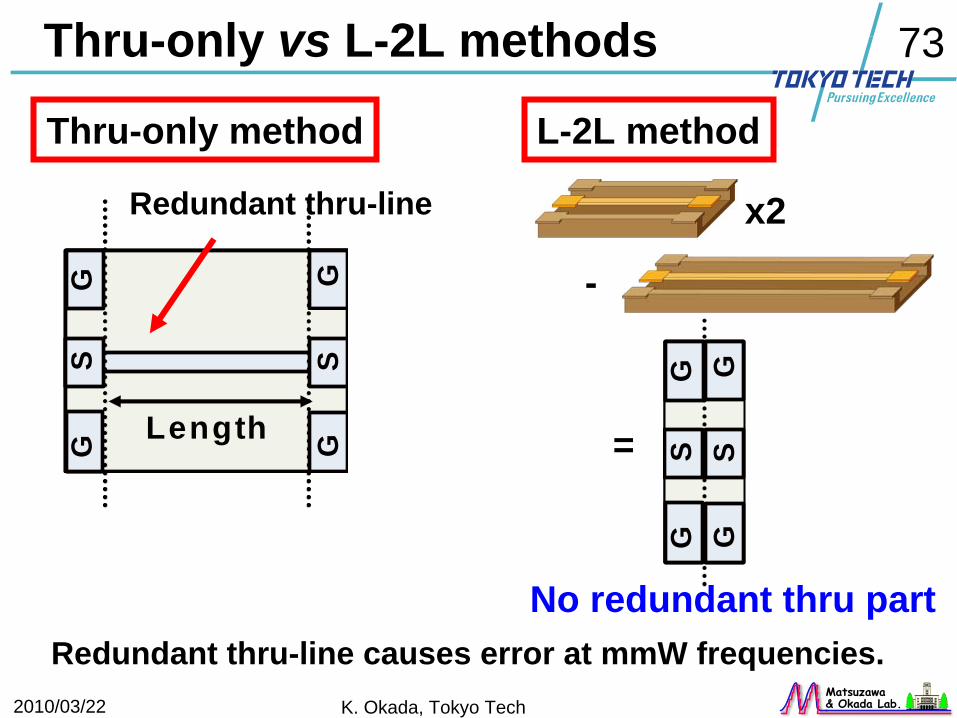
Thru-only vs L-2L methodsS
GG G
SGLength
SG
G GS
GLength
Thru-only method L-2L method
Redundant thru-line causes error at mmW frequencies.
Redundant thru-line x2
-
SG
G GS
GS
GG G
SG
=
No redundant thru part
2010/03/22 K. Okada, Tokyo Tech
74
Matsuzawa& Okada Lab.
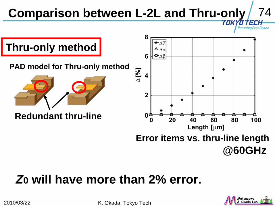
Comparison between L-2L and Thru-only
Error items vs. thru-line length
PAD model for Thru-only method
Z0 will have more than 2% error.
Redundant thru-line
Thru-only method
@60GHz
2010/03/22 K. Okada, Tokyo Tech
75
Matsuzawa& Okada Lab.
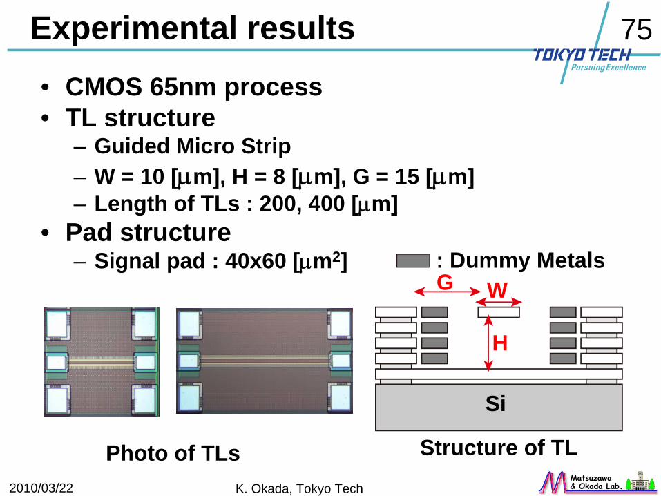
Experimental results• CMOS 65nm process• TL structure
– Guided Micro Strip– W = 10 [μm], H = 8 [μm], G = 15 [μm]– Length of TLs : 200, 400 [μm]
• Pad structure– Signal pad : 40x60 [μm2]
Structure of TLPhoto of TLs
Si
H
G W: Dummy Metals
2010/03/22 K. Okada, Tokyo Tech
76
Matsuzawa& Okada Lab.
Verification
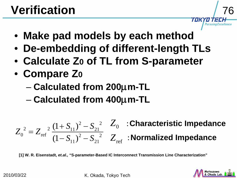
[1] W. R. Eisenstadt, et.al., “S-parameter-Based IC Interconnect Transmission Line Characterization”
0
ref
ZZ :Normalized Impedance
:Characteristic Impedance
• Make pad models by each method• De-embedding of different-length TLs• Calculate Z0 of TL from S-parameter• Compare Z0
– Calculated from 200μm-TL– Calculated from 400μm-TL
2 22 2 11 21
0 ref 2 211 21
(1 )(1 )
S SZ ZS S
+ −=
− −
2010/03/22 K. Okada, Tokyo Tech
77
Matsuzawa& Okada Lab.
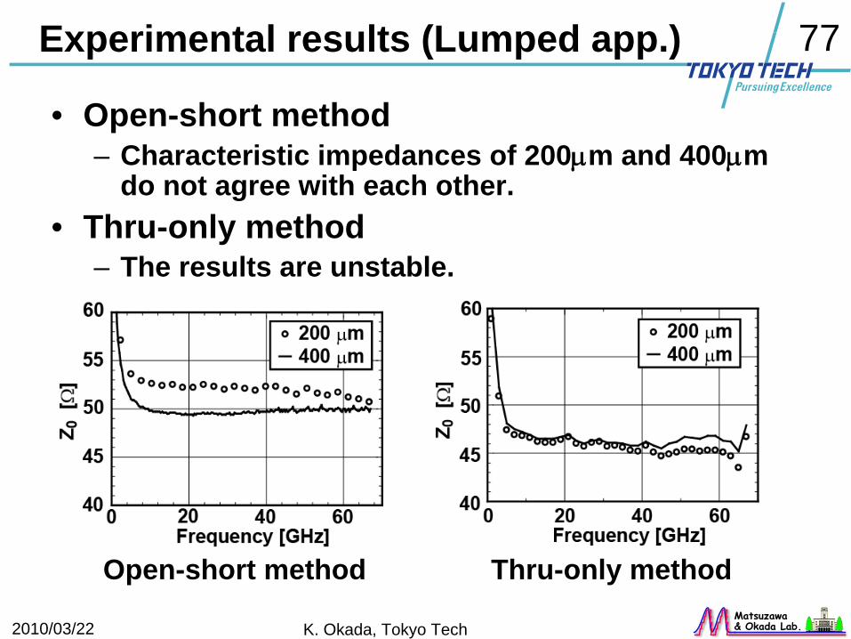
Experimental results (Lumped app.)
• Open-short method– Characteristic impedances of 200μm and 400μm
do not agree with each other.• Thru-only method
– The results are unstable.
Open-short method Thru-only method
2010/03/22 K. Okada, Tokyo Tech
78
Matsuzawa& Okada Lab.
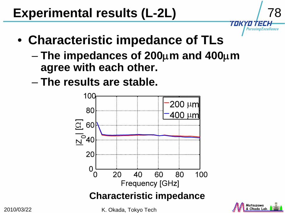
Experimental results (L-2L)
• Characteristic impedance of TLs– The impedances of 200μm and 400μm
agree with each other.– The results are stable.
Characteristic impedance
2010/03/22 K. Okada, Tokyo Tech
79
Matsuzawa& Okada Lab.
Summary
• Lumped/Distributed de-embedding methods are reviewed.
• L-2L method performs very high accuracy at mmW frequency.
• The conventional Open-Short fails.
2010/03/22 K. Okada, Tokyo Tech
80
Matsuzawa& Okada Lab.
Outline
• Motivation• Issues for mmW CMOS Circuits• Device Characterization• De-embedding• Conclusion
2010/03/22 K. Okada, Tokyo Tech
81
Matsuzawa& Okada Lab.
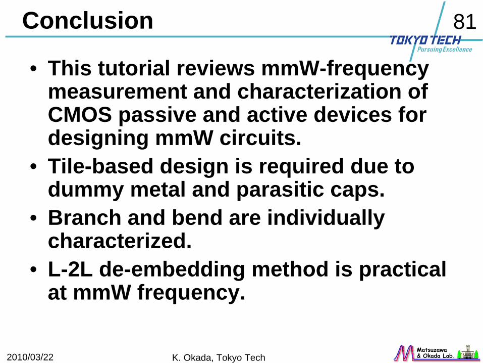
Conclusion
• This tutorial reviews mmW-frequency measurement and characterization of CMOS passive and active devices for designing mmW circuits.
• Tile-based design is required due to dummy metal and parasitic caps.
• Branch and bend are individually characterized.
• L-2L de-embedding method is practical at mmW frequency.
2010/03/22 K. Okada, Tokyo Tech
82
Matsuzawa& Okada Lab.
Acknowledgement
This work is partially supported by MIC, STARC, NEDO, and VDEC in collaboration with Cadence Design Systems, Inc., and Agilent Technologies Japan, Ltd.
Special thanks to Dr.Joshin, Dr.Hirose, Dr.Suzuki, Dr.Sato, and Dr.Kawano of FUJITSU Lab., Ltd. for their fruitful discussion.