nanometer cmos goes millimeter wave - core nanometer cmos goes millimeter wave 2 overview ... ref....
TRANSCRIPT

Nanometer CMOS goes Nanometer CMOS goes millimeter wavemillimeter wave
N.DefermN.Deferm, , P.ReynaertP.Reynaert

09/07/200909/07/2009 Nanometer CMOS goes millimeter waveNanometer CMOS goes millimeter wave 22
OverviewOverview
IntroductionIntroductionActive devicesActive devicesMatchingMatchingExamplesExamplesConclusionConclusion

09/07/200909/07/2009 Nanometer CMOS goes millimeter waveNanometer CMOS goes millimeter wave 33
OverviewOverview
IntroductionIntroductionActive devicesActive devicesMatchingMatchingExamplesExamplesConclusionConclusion

09/07/200909/07/2009 Nanometer CMOS goes millimeter waveNanometer CMOS goes millimeter wave 44
IntroductionIntroductionSurveillanceSurveillance
/security/security
Medical Medical ImagingImaging
Guiding ofGuiding ofvehiclesvehicles

09/07/200909/07/2009 Nanometer CMOS goes millimeter waveNanometer CMOS goes millimeter wave 55
IntroductionIntroductionAll nice and fancy applications, but letAll nice and fancy applications, but let’’s get to the s get to the serious part of the story: serious part of the story:
Design of mm-wave integrated circuits
CMOS integrated circuits for mmCMOS integrated circuits for mm--wave applications:wave applications:Analog, Digital and RF circuits on the same dieAnalog, Digital and RF circuits on the same dieSize and cost reduction for large volumesSize and cost reduction for large volumesNew mmNew mm--wave system topologies are becoming wave system topologies are becoming possible, e.g. complete beam forming architecturepossible, e.g. complete beam forming architecture

09/07/200909/07/2009 Nanometer CMOS goes millimeter waveNanometer CMOS goes millimeter wave 66
Fully integrated systemFully integrated systemUse CMOS to reduce the size & costof mm-wave mass-volume electronics

09/07/200909/07/2009 Nanometer CMOS goes millimeter waveNanometer CMOS goes millimeter wave 77
Fully integrated systemFully integrated system
Fully integrated beam forming transceiver @ mm-wave frequencies is becoming possible

09/07/200909/07/2009 Nanometer CMOS goes millimeter waveNanometer CMOS goes millimeter wave 88
OverviewOverview
IntroductionIntroductionActive devicesActive devicesPassive devicesPassive devicesExamplesExamplesConclusionConclusion

09/07/200909/07/2009 Nanometer CMOS goes millimeter waveNanometer CMOS goes millimeter wave 99
CMOS goes mmCMOS goes mm--wavewaveITRS roadmap for fTMeasured values of fmax
CMOS becomes a mm-wave technology?
Yes, but with a very high integration density
Waf
er s
ize
Inte
grat
ion
dens
ity

09/07/200909/07/2009 Nanometer CMOS goes millimeter waveNanometer CMOS goes millimeter wave 1010
MOS fMOS ftt and fand fmaxmax
90nm CMOS transistor90nm CMOS transistor
Next technology nodes will reach even higher Next technology nodes will reach even higher frequencies and gain.frequencies and gain.
Masongain = 10db @ 100GHz
ft = 130GHz
fmax = 260GHz

09/07/200909/07/2009 Nanometer CMOS goes millimeter waveNanometer CMOS goes millimeter wave 1111
MOS fMOS ftt and fand fmaxmax
fftt = frequency at which current gain equals unity => |h= frequency at which current gain equals unity => |h2121|=1|=1
( )in gs gs gdi v j C Cω= ⋅ +out gs mi v g≈ ⋅
( )2m
tgs gd
gfC Cπ
=⋅ +
ffmaxmax = frequency at which power gain equals unity= frequency at which power gain equals unity
8t
maxg gd
ffr Cπ
≈⋅ ⋅
Definition fmax: Ref. W. Sansen: analog design essentials, p.33
Push fmax towards higher frequencies by reducing rg
09/07/200909/07/2009 Nanometer CMOS goes millimeter waveNanometer CMOS goes millimeter wave 1212
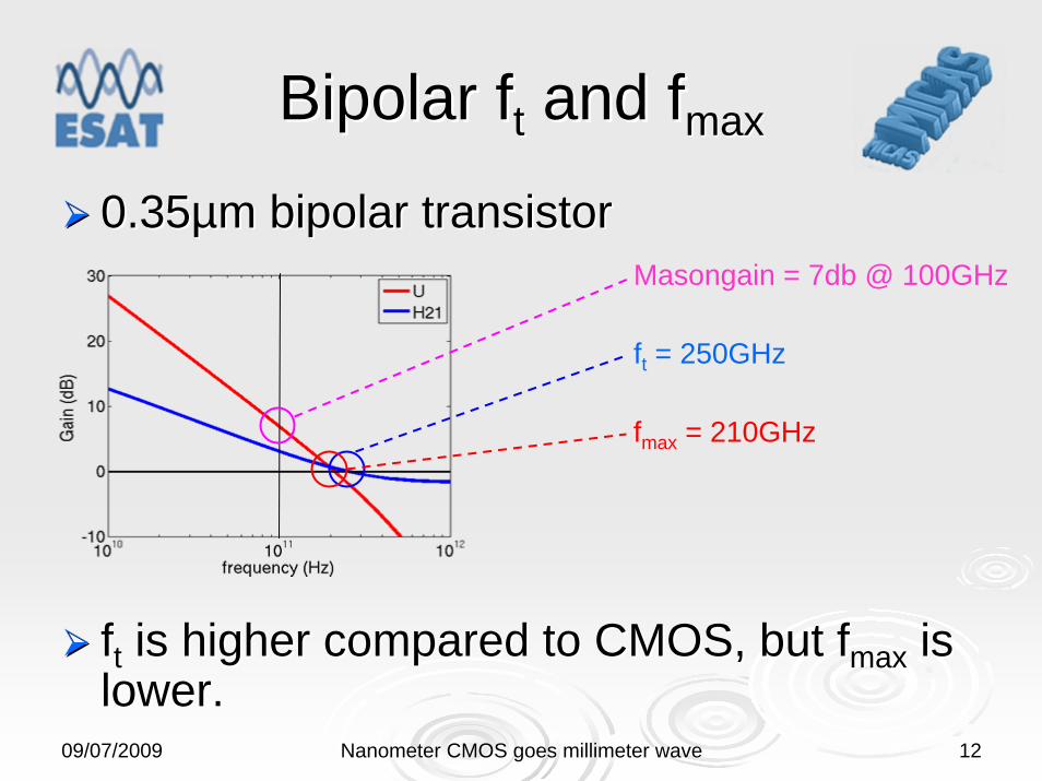
0.350.35µµm bipolarm bipolar transistortransistor
fftt is higher compared to CMOS, but fis higher compared to CMOS, but fmaxmax is is lower.lower.
Bipolar fBipolar ftt and fand fmaxmax
Masongain = 7db @ 100GHz
ft = 250GHz
fmax = 210GHz

09/07/200909/07/2009 Nanometer CMOS goes millimeter waveNanometer CMOS goes millimeter wave 1313
Bipolar fBipolar ftt and fand fmaxmaxfftt = frequency at which current gain equals unity => |h= frequency at which current gain equals unity => |h2121|=1|=1
1in be
be
i v j C
v j Cr
μ
ππ
ω
ω
= ⋅ ⋅
⎛ ⎞ + ⋅ ⋅ +⎜ ⎟
⎝ ⎠
out be mi v g≈ ⋅
( )2m
tgfC Cμ ππ
≈⋅ +
ffmaxmax = frequency at which power gain equals unity= frequency at which power gain equals unity
8t
maxb
ffr Cμπ
≈⋅ ⋅
Definition fmax: Ref. W. Sansen: Analog Design Essentials, p.43
reducing rb by increasing emitter length => Cµ increases => fmax is not improving

09/07/200909/07/2009 Nanometer CMOS goes millimeter waveNanometer CMOS goes millimeter wave 1414
CMOS vs. bipolarCMOS vs. bipolarComparison at equal power Comparison at equal power consumption of 4mWconsumption of 4mWMOS (W=15MOS (W=15µµm)m) => fmax => fmax from 100GHz to 260GHz from 100GHz to 260GHz when decreasing rwhen decreasing rgg. . (260GHz is maximum (260GHz is maximum achievable)achievable)Bipolar => fmax from Bipolar => fmax from 210GHz to 170GHz when 210GHz to 170GHz when decreasing rdecreasing rbb. (210GHz is . (210GHz is maximum achievable)maximum achievable)
fmax MOS can be pushed towards higher frequencies
fmax bipolar
fmax MOS

09/07/200909/07/2009 Nanometer CMOS goes millimeter waveNanometer CMOS goes millimeter wave 1515
Transistor behaviorTransistor behaviorGGmaxmax vs. U: how to get the maximal out of the vs. U: how to get the maximal out of the transistor?transistor?U: measure for U: measure for maximum maximum achievable gainachievable gainGGmaxmax: actual gain of : actual gain of the transistorthe transistor
unconditionally stable region
conditionally stable region
Goal: shift stability break point towards wanted frequency of operation

09/07/200909/07/2009 Nanometer CMOS goes millimeter waveNanometer CMOS goes millimeter wave 1616
Transistor behaviorTransistor behavior
Increase U, fmax and stability break point by reducing gate resistance
Increase Gmax by tuning the gate-drain capacitance
Gain increase from 0dB to 11dB @ 100GHz by the use of circuit techniques.
Note: power consumption is kept constant @ 4mW

09/07/200909/07/2009 Nanometer CMOS goes millimeter waveNanometer CMOS goes millimeter wave 1717
Transistor behaviorTransistor behavior
Lowering base resistance results in a decrease of U and fmax due to increase of Cµ.
Gain loss from 6dB to 4dB@ 100GHz. Highest gain achieved with minimal size transistor.
Note: power consumption is kept constant @ 4mW

09/07/200909/07/2009 Nanometer CMOS goes millimeter waveNanometer CMOS goes millimeter wave 1818
OverviewOverview
IntroductionIntroductionActive devicesActive devicesMatchingMatchingExamplesExamplesConclusionConclusion

09/07/200909/07/2009 Nanometer CMOS goes millimeter waveNanometer CMOS goes millimeter wave 1919
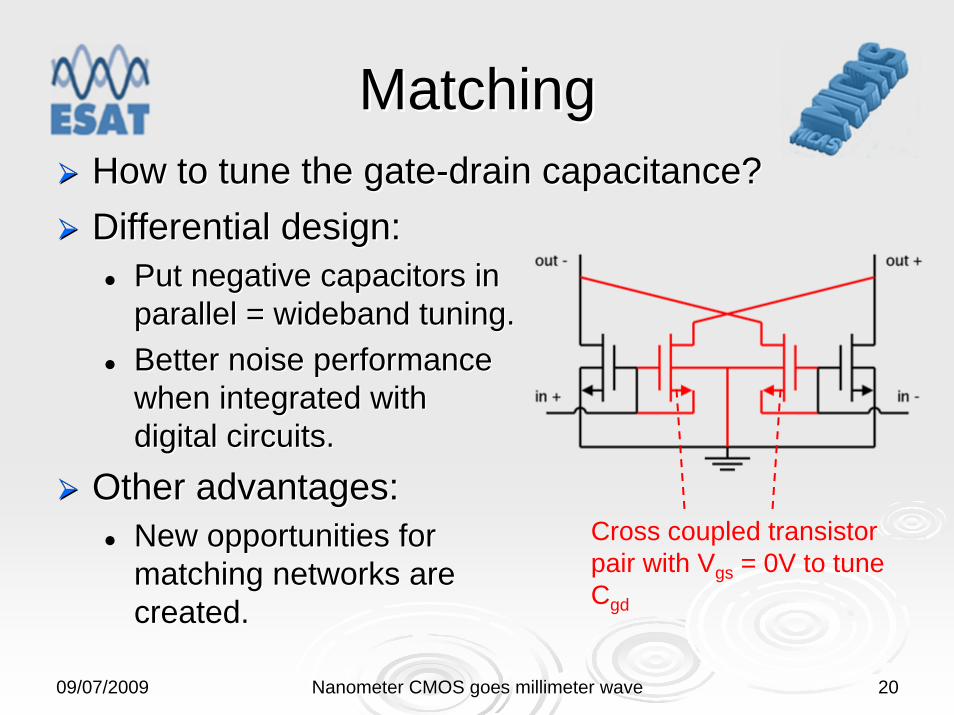
MatchingMatchingTuning of input/output capacitors reveals resistors.Tuning of input/output capacitors reveals resistors.Maximize power transfer from source to device and from Maximize power transfer from source to device and from device to load by power matching.device to load by power matching.
RRss = r= rggRRloadload = r= rdsds
Tuning elements can be included in the matching Tuning elements can be included in the matching network.network.
Ls tunes Cgs
Lload tunes Cds
09/07/200909/07/2009 Nanometer CMOS goes millimeter waveNanometer CMOS goes millimeter wave 2020
MatchingMatchingHow to tune the gateHow to tune the gate--drain capacitance?drain capacitance?Differential design: Differential design:
Put negative capacitors in Put negative capacitors in parallel = wideband tuning.parallel = wideband tuning.Better noise performance Better noise performance when integrated with when integrated with digital circuits.digital circuits.
Other advantages:Other advantages:New opportunities for New opportunities for matching networks are matching networks are created.created.
Cross coupled transistor pair with Vgs = 0V to tune Cgd

09/07/200909/07/2009 Nanometer CMOS goes millimeter waveNanometer CMOS goes millimeter wave 2121
TransformersTransformersIntegrated transformers Integrated transformers in 90nm CMOS:in 90nm CMOS:
Minimum insertion loss Minimum insertion loss lower than 1dB.lower than 1dB.Easy DC biasing and Easy DC biasing and connect supply voltages.connect supply voltages.Inherent DC blocking Inherent DC blocking ability.ability.Can be used to connect Can be used to connect differential networks to differential networks to other differential networks other differential networks and single ended ones.and single ended ones. Ref: D. Chowdhury et. al., IEEE ISSCC 2008
40µm
8µm

09/07/200909/07/2009 Nanometer CMOS goes millimeter waveNanometer CMOS goes millimeter wave 2222
Transformers and Transformers and matchingmatching
Adaptation of size and shape can create the Adaptation of size and shape can create the ability of impedance transformation.ability of impedance transformation.
Stage 1
Stage 2
Gate bias stage 2: connected to inner coil center tap
Supply voltage stage 1: connected to outer coil center tap
Local ground stage 1
Local ground stage 2
55µm
110µm

09/07/200909/07/2009 Nanometer CMOS goes millimeter waveNanometer CMOS goes millimeter wave 2323
OverviewOverview
IntroductionIntroductionActive devicesActive devicesMatchingMatchingExamplesExamplesConclusionConclusion

09/07/200909/07/2009 Nanometer CMOS goes millimeter waveNanometer CMOS goes millimeter wave 2424
Example 1: 60 GHz VCOExample 1: 60 GHz VCO570 um
620 um
90nm CMOS
Area: 0.35 mm2 includingprobe-padsTuning range: 61.1-66.7GHz Phase noise @ 1MHz from64GHz: -95dBc/HzPower consumption: 3.16mW@ 0.6V supply

09/07/200909/07/2009 Nanometer CMOS goes millimeter waveNanometer CMOS goes millimeter wave 2525
Example 2: Differential Example 2: Differential 60 GHz PA60 GHz PA
Area: 0.25 mm2 including probe-padsGain: 7.7dB @ 48GHzPower consumption: 100mW @ 1V supply
Output power: 12.3dBm3dB BW: 22GHz (43-65GHz)

09/07/200909/07/2009 Nanometer CMOS goes millimeter waveNanometer CMOS goes millimeter wave 2626
Example 3: Differential Example 3: Differential 100 GHz amplifier100 GHz amplifier
Input stage DC pads Interstage DC pads Output stage DC pads
RF input
RF output
650µm
1.4mmArea: 0.84 mm2 including probe-padsPower consumption: 50mW @ 1V supply
Gain: 15dB @ 92 GHz3dB BW: 15GHz (87-102GHz)
Simulation results

09/07/200909/07/2009 Nanometer CMOS goes millimeter waveNanometer CMOS goes millimeter wave 2727
Example 4: 410 GHz Example 4: 410 GHz pushpush--push oscillatorpush oscillator
CMOS world record at 410 GHz
200 GHz higher than existingCMOS record.100 GHz higher than highperformance expensive indiumphosphide chips.
45nm CMOS 410 GHz push-pushoscillator operating at 2nd harmonic.

09/07/200909/07/2009 Nanometer CMOS goes millimeter waveNanometer CMOS goes millimeter wave 2828
OverviewOverview
IntroductionIntroductionActive devicesActive devicesMatchingMatchingExamplesExamplesConclusionConclusion

09/07/200909/07/2009 Nanometer CMOS goes millimeter waveNanometer CMOS goes millimeter wave 2929
ConclusionConclusionCMOS will play an important role in mmCMOS will play an important role in mm--wave wave imaging applications (large volumes needed).imaging applications (large volumes needed).CMOS is very flexible from circuit design point of CMOS is very flexible from circuit design point of view: reasonable gain feasible at mmview: reasonable gain feasible at mm--wave wave frequencies by employing circuit techniques.frequencies by employing circuit techniques.Differential design creates numerous Differential design creates numerous advantages including new tuning and matching advantages including new tuning and matching techniques.techniques.Full integration of complete mmFull integration of complete mm--wave systems wave systems becomes possible.becomes possible.