high speed ldo regulators, low esr cap the typical application circuit for the kx8100...
TRANSCRIPT
V01 Page 1 of 9
HighHighHighHigh PerformancePerformancePerformancePerformance Off-LineOff-LineOff-LineOff-Line ControllerControllerControllerController
GeneralGeneralGeneralGeneral DescriptionDescriptionDescriptionDescription FeaturesFeaturesFeaturesFeatures
KX8100 Series is a high performance green-energyoffline power supply controller. It features a scalabledriver for driving external NPN or MOSFETtransistors for line voltage switching. This proprietaryarchitecture enables many advanced features to beintegrated into a small package(TO-92),resulting inlowest total cost solution.The KX8100 design has 6 internal terminals and is apulse frequency and width modulation IC with manyflexible packaging options. One combination ofinternal terminals is packaged in the space-savingTO-92 package (A/B versions) for 65kHz switchingfrequency and with 400mA or 800mA current limit.Consuming only 0.15W in standby, the IC featuresover-current, hiccup mode short circuit, and under-voltage protection mechanisms.The KX8100 is ideal for use in high performanceuniversal adaptors and chargers.
Lowest Total Cost Solution 0.15W Standby Power Emitter Drive Allows Safe NPN Flyback Use Hiccup Mode Short Circuit Current Mode Operation Over-Current Protection Under-voltage Protection with Auto-restart Proprietary Scalable Output Driver Flexible Packaging Options(including TO-92) 65kHz Switching Frequency Selectable 0.4A to 0.8A Current Limit
TypicalTypicalTypicalTypical ApplicationApplicationApplicationApplication Battery Chargers Power Adaptors Standby Power Supplies Appliances Universal Off-line Power Supplies
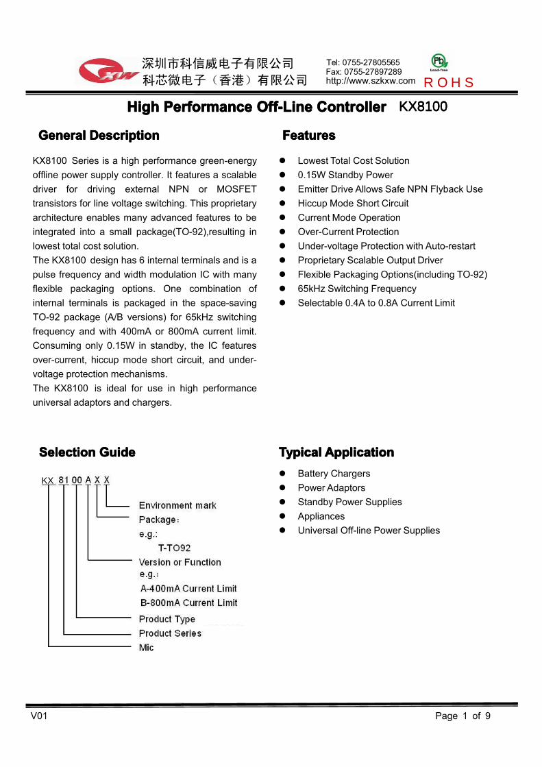
SelectionSelectionSelectionSelection GuideGuideGuideGuide
深圳市科信威电子有限公司
科芯微电子(香港)有限公司
Tel: 0755-27805565 Fax: 0755-27897289 http://www.szkxw.com ROHS
KX8100KX8100KX8100
KX

V01 Page 2 of 9
TypicalTypicalTypicalTypical ApplicationApplicationApplicationApplication CircuitCircuitCircuitCircuit
L F 1C1
R2 R3 C3
D5
T1
D6R5
C1 3
D1 1
R2 1
C9 C 1 0
P C 8 1 7
R1 1
T L 4 3 1
R 1 6
V O U T +
D3
D4
R1
L1
C2
V D 1Q1
D7 R6
C4
C6
D R V
G N D
L2
R 1 2
R1 7R 1 9
Q2
V O U T -
V A C _I N
V D D
KX 8 1 0 0
C5
R8
D1D
2
PinPinPinPin ConfigurationConfigurationConfigurationConfiguration&&&& PinPinPinPinAssignmentAssignmentAssignmentAssignment
PPPPinininin NNNNumberumberumberumberPPPPinininin NNNNameameameame FFFFunctionunctionunctionunction
TO-92
1 VDDPower Supply Pin. Connect to optocoupler's emitter. Internally limited to 5.5Vmax. Bypass to GND with a proper compensation network.
2 GND Ground
3 DRVDriver Output (TO-92 Only). Connect to emitter of the high voltage NPN orMOSFET.
深圳市科信威电子有限公司
科芯微电子(香港)有限公司
Tel: 0755-27805565 Fax: 0755-27897289 http://www.szkxw.com ROHS
KX8100
V01 Page 3 of 9
AbsoluteAbsoluteAbsoluteAbsolute MaximumMaximumMaximumMaximum RatingsRatingsRatingsRatings
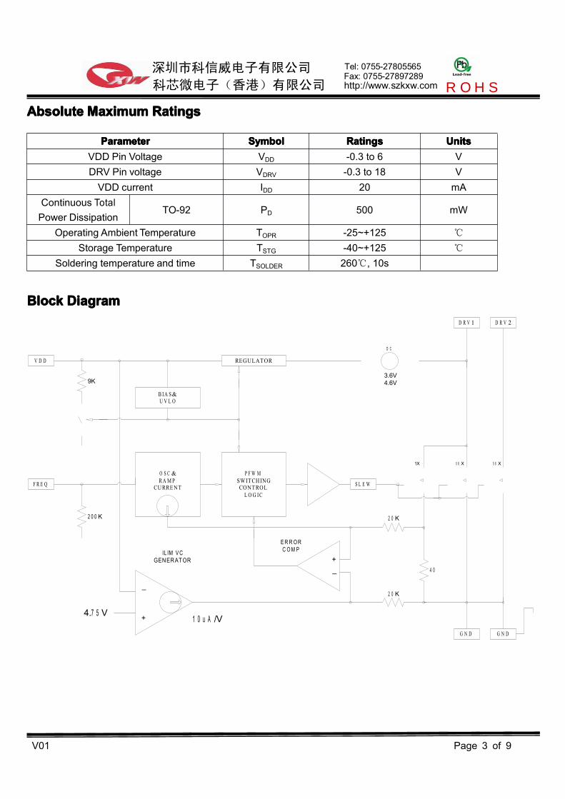
BlockBlockBlockBlock DiagramDiagramDiagramDiagram
V D D REGULATOR
D C
D R V 1 D R V 2
9K
1X 5 6 X 5 6 X
G N D G N D
3.6V4.6V
B IA S&U V L O
O S C &RAMP
CURRENT
P F W MSWITCHINGCONTROLLOG IC
S L E WF R E Q
2 0 0 K
_
+4.7 5 V1 0 u A /V
4 0
2 0 K
2 0 K
_+
E R R O RC O M PIL IM V C
GENERATOR
ParameterParameterParameterParameter SSSSymbolymbolymbolymbol RRRRatingsatingsatingsatings UUUUnitsnitsnitsnitsVDD Pin Voltage VDD -0.3 to 6 VDRV Pin voltage VDRV -0.3 to 18 V
VDD current IDD 20 mAContinuous Total
Power DissipationTO-92 PD 500 mW
Operating Ambient Temperature TOPR -25~+125
Storage Temperature TSTG -40~+125
Soldering temperature and time TSOLDER 260, 10s
深圳市科信威电子有限公司
科芯微电子(香港)有限公司
Tel: 0755-27805565 Fax: 0755-27897289 http://www.szkxw.com ROHS

V01 Page 4 of 9
ElectricalElectricalElectricalElectrical CharacteristicsCharacteristicsCharacteristicsCharacteristicsKX8100AXX/BXX (Measuring conditions:Unless otherwise specified , VIN=4V,TOPT=25)
SSSSymbolymbolymbolymbol ParameterParameterParameterParameter ConditionsConditionsConditionsConditions MMMMinininin TTTTyp.yp.yp.yp. MaxMaxMaxMax UUUUnitsnitsnitsnits
VSTART VDD Star Voltage Rising edge 4.75 5 5.25 V
VDRVST DRV Start VoltageDRV must be higher than
this voltage to star up9 11 V
VSCDRVDRV Short-Circuit DetectThreshold
5.8 V
VUVVDD Under-voltageThreshold
Falling edge 3.17 3.35 3.53 V
VDD Clamp Voltage 10mA 5.15 5.45 5.75 V
IDDST Startup Supply Current VDD=4V before VUV 0.15 0.45 mA
IDD Supply Current 0.4 1.0 mA
FSW Switching Frequency FREQ=0 50 60 80 KHz
DMAX Maximum Duty Cycle VDD=4VME8100A 67 75 83
%ME8100B 60
DMIN Minimum Duty Cycle VDD=4.6V 5.5
ILIM Effective Current LimitVDD=VUV
+0.1vME8100A 400
mAME8100B 800
GGAINVDD to DRV CurrentCoefficient
-0.2 A/V
RVDD VDD Dynamic Impedance 9 kΩ
DRV Rise Time 1nF load,15Ω pull-up 30 ns
DRV Fall Time 1nF load,15Ω pull-up 20 ns
深圳市科信威电子有限公司
科芯微电子(香港)有限公司
Tel: 0755-27805565 Fax: 0755-27897289 http://www.szkxw.com ROHS

V01 Page 5 of 9
FunctionFunctionFunctionFunction DescriptionDescriptionDescriptionDescription StartupStartupStartupStartup SequenceSequenceSequenceSequence
As the Functional Block Diagram of the KX8100The main components include switching control logic,two on-chip Medium-voltage power-MOSFETs withparallel current sensor, driver, oscillator and rampgenerator, current limit VC generator, error comparator,hiccup control, bias and undervoltage-lockout, andregulator circuitry.
The design has 6 internal terminals. VDD is thepower supply terminal.DRV1 and DRV2 are lineardriver outputs that can drive the emitter of an externalhigh voltage NPN transistor or N-channel MOSFET.This emitter-drive method takes advantage of the highVCBO of the transistor, allowing a low cost transistorsuch as 13003 (VCBO = 700V) or 13002 (VCBO =
600V) to be used for a wide AC input range. The slew-rate limited driver coupled with the turn-offcharacteristics of an external NPN result in lower EMI.
The driver peak current is designed to have anegative voltage coefficient with respect to supplyvoltage VDD, so that lower supply voltageautomatically results in higher DRV1 peak current. Thisway, the optocoupler can control VDD directly to affectdriver current.
As the typical application Circuit for the KX8100Initially, the small current through resistor R2 chargesup the capacitor C4, and the BJT acts as a follower tobring up the DRV1 voltage. An internal regulatorgenerates a VDD voltage equal to VDRV1-3.6V forKX8100A (VDRV1-4.6V for KX8100B but limits it to5.5VMAX. As VDD crosses 5V, the regulator sourcingfunction stops and VDD begins to drop due to itscurrent consumption. As VDD voltage decreasesbelow 4.75V, the IC starts to operate with increasingdriver current. When the output voltage reachesregulation point, the optocoupler feedback circuit stopsVDD from decreasing further. The switching actionalso allows the auxiliary windings to take over insupplying the C4 capacitor. The following sketch mapshows a typical startup sequence for the KX8100
To limit the auxiliary voltage, use a 12V zener diodefor KX8100A or a 13V zener for KX8100B (VD1 diodein Typical Application).
Even though up to 2MΩ startup resistor (R2) can beused due to the very low startup current, the actual R2value should be chosen as a compromise betweenstandby power and startup time delay.
深圳市科信威电子有限公司
科芯微电子(香港)有限公司
Tel: 0755-27805565 Fax: 0755-27897289 http://www.szkxw.com ROHS

V01 Page 6 of 9
NormalNormalNormalNormal OperationOperationOperationOperation CurrentCurrentCurrentCurrent limitlimitlimitlimit adjustmentadjustmentadjustmentadjustment
In normal operation, the feedback signal from thesecondary side is transmitted through the optocoupleras a current signal into VDD pin, which has dynamicimpedance of 9kΩ. The resulting VDD voltage affectsthe switching of the IC. As seen from the FunctionalBlock Diagram, the Current Limit VC Generator usesthe VDD voltage difference with 4.75V to generate aproportional offset at the negative input of the ErrorComparator.
The drivers turn on at the beginning of eachswitching cycle. The current sense resistor current,which is a fraction of the transformer primary current,increases with time as the primary current increases.When the voltage accross this current sense resistorplus the oscillator ramp signal equals ErrorComparator's negative input voltage, the drivers turnoff. Thus, the peak DRV1 current has a negativevoltage coefficent of -0.29A/V and can be calculatedfrom the following:
IDRV1PEAK = 0.2A/V×(4.75V – VDD)for VDD<4.75V and duty cycle<50%.When the outputvoltage is lower than regulation, the current into VDDpin is zero and VDD voltage decreases. At VDD = VUV= 3.35V, the peak DRV1 current has maximum value of400mA.
PulsePulsePulsePulse skippingskippingskippingskippingThe PFWM Switching Control Logic block operates indifferent modes depending on the output load currentlevel. At light load, the VDD voltage is around 4.75V.The energy delivered by each switching cycle (withminimum on time of 500ns) to the output causes VDD
to increase slightly above 4.75V. The FPWMSwitching Control Logic block is able to detect thiscondition and prevents the IC from switching until VDD
is below 4.75V again. This results in a pulse-skippingaction with fixed pulse width and varying frequency,and low power consumption because the switchingfrequency is reduced.Typical system standby powerconsumption is 0.15W.
DDDDriverriverriverriver outputoutputoutputoutput configurationsconfigurationsconfigurationsconfigurationsThe IC's proprietary driver arrangement allows the
current limit to be easily adjusted between 400mA and1.2A. To understand this, the drivers have to be utilizedas linear resistive devices with typically 3.6Ω (ratherthan as digital output switches). The current limit canthen be calculated through linear combination asshown in the front. For TO-92 package, the KX8100Aare preprogrammed to 400mA current limit and theKX8100 are preprogrammed to 800mA current limit.
深圳市科信威电子有限公司
科芯微电子(香港)有限公司
Tel: 0755-27805565 Fax: 0755-27897289 http://www.szkxw.com ROHS
V01 Page 7 of 9
PackagingPackagingPackagingPackaging InformationInformationInformationInformation
ShortShortShortShort circuitcircuitcircuitcircuit hiccuphiccuphiccuphiccupWhen the output is short circuited, the KX8100
enters hiccup mode operation. In this condition,theauxiliary supply voltage collapses. An on-chip detectorcompares DRV1 voltage during the off-time of eachcycle to 6.8V. If DRV1 voltage is below 6.8V, the IC willnot start the next cycle, causing both the auxiliarysupply voltage and VDD to reduce further. The circuitenters startup mode when VDD drops below 3.35V.This hiccup behaviour continues until the short circuitis removed. In this behavior, the effective duty cycle isvery low resulting in very low short circuit current.
To make sure that the IC enters hiccup mode easily,the transformer should be constructed so that there isclose coupling between secondary and auxiliary, sothat the auxiliary voltage is low when the output isshort-circuited. This can be achieved with theprimary/auxiliary/secondary sequencing from thebobbin.
AAAApplicationpplicationpplicationpplication informationinformationinformationinformation ExternalExternalExternalExternal powerpowerpowerpower transistortransistortransistortransistor
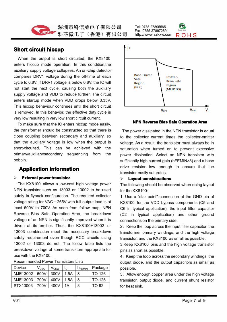
The KX8100 allows a low-cost high voltage powerNPN transistor such as 13003 or 13002 to be usedsafely in flyback configuration. The required collectorvoltage rating for VAC=265V with full output load is atleast 600V to 700V. As seen from follow map, NPNReverse Bias Safe Operation Area, the breakdownvoltage of an NPN is significantly improved when it isdriven at its emitter. Thus, the KX8100+13002 or13003 combination meet the necessary breakdownsafety requirement even though RCC circuits using13002 or 13003 do not. The follow table lists thebreakdown voltage of some transistors appropriate foruse with the KX8100.Recommended Power Transistors List:Device VCBO VCEO IC hFEMIN PackageMJE13002 600V 300V 1.5A 8 TO-126MJE13003 700V 400V 1.5A 8 TO-126STX13003 700V 400V 1A 8 TO-92
NPNNPNNPNNPN ReverseReverseReverseReverse BiasBiasBiasBias SafeSafeSafeSafe OperationOperationOperationOperation AreaAreaAreaArea
The power dissipated in the NPN transistor is equalto the collector current times the collector-emittervoltage. As a result, the transistor must always be insaturation when turned on to prevent excessivepower dissipation. Select an NPN transistor withsufficiently high current gain (hFEMIN>8) and a basedrive resistor low enough to ensure that thetransistor easily saturates. LLLLayoutayoutayoutayout considerationsconsiderationsconsiderationsconsiderationsThe following should be observed when doing layoutfor the KX8100:1. Use a "star point" connection at the GND pin ofKX8100 for the VDD bypass components (C5 andC6 in typical application), the input filter capacitor(C2 in typical application) and other groundconnections on the primary side.2.Keep the loop across the input filter capacitor, thetransformer primary windings, and the high voltagetransistor, and the KX8100 as small as possible.3.Keep KX8100 pins and the high voltage transistorpins as short as possible.4.Keep the loop across the secondary windings, theoutput diode, and the output capacitors as small aspossible.5.Allow enough copper area under the high voltagetransistor, output diode, and current shunt resistorfor heat sink.
深圳市科信威电子有限公司
科芯微电子(香港)有限公司
Tel: 0755-27805565 Fax: 0755-27897289 http://www.szkxw.com ROHS
V01 Page 8 of 9
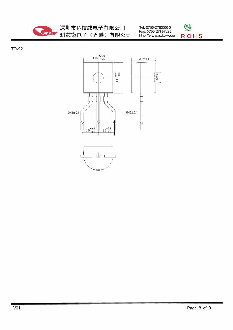
TO-92
深圳市科信威电子有限公司
科芯微电子(香港)有限公司
Tel: 0755-27805565 Fax: 0755-27897289 http://www.szkxw.com ROHS