high-speed serial interface - yonsei...
TRANSCRIPT

High-speed Serial Interface
Lect. 6 – TX Driver and Equalizer
2013-1High-Speed Circuits and Systems Lab., Yonsei University1

Block diagram
2013-1High-Speed Circuits and Systems Lab., Yonsei University2
Serializer Sampler
ClockRecovery
Deserializer
PLL
Channel
Tx Rx
• Where are we today?
RxEqualizer
TxDriver

Classic output driver• An inverter can be used as voltage-mode output
driver
2013-1High-Speed Circuits and Systems Lab., Yonsei University3
TTL output buffer CMOS output buffer
R R

Classic output driver• It is difficult to use inverter-style output driver in
high-speed applications
– Full-swing logic is speed-limited because of slow switching time of inverter-style driver
– Impedance matching is not easy• Transistors have variable output resistances during output voltage
transients
2013-1High-Speed Circuits and Systems Lab., Yonsei University4

Single-ended signaling• Signal is transferred via single channel• Simple but …• Threshold should be generated in RX side.
– Logic levels in TX may not be same as in RX side• Supply and ground levels are different for RX and RX sides
• Poor noise immunity– Noises are added while signals travel through channel
2013-1High-Speed Circuits and Systems Lab., Yonsei University5
50-Ω ChannelThresholdgenerated
in RX
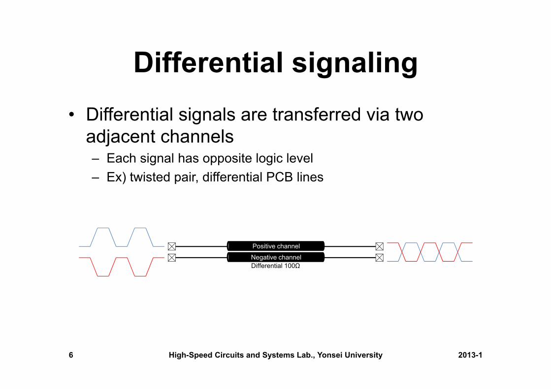
Differential signaling• Differential signals are transferred via two
adjacent channels– Each signal has opposite logic level– Ex) twisted pair, differential PCB lines
2013-1High-Speed Circuits and Systems Lab., Yonsei University6
Positive channel
Negative channelDifferential 100Ω

Differential signaling• Larger signal swing and self-reference
– Signal = (positive signal – negative signal)Decision margin enhanced
– threshold= (positive signal + negative signal)/2
• Common-mode noise rejection– Noise usually affects both positive and negative channels– Subtraction rejects common-mode noise
2013-1High-Speed Circuits and Systems Lab., Yonsei University7
Positive channel
Negative channel
Common-modenoise
Differential 100Ω

Current-mode driver• Reduced switching time
– Current-steering: Switching current path while source current is kept constant.
– Switching time is reduced since current source is not turned-off
• Disadvantage– Differential signaling is required.– Static current causes
static power consumption Usually larger power consumption
than voltage-mode
2013-1High-Speed Circuits and Systems Lab., Yonsei University8
I+ I-
Ibias

50-Ω termination• Why 50Ω?
– Historical issue
• In early microwave systems, it was known that– 33Ω shows best performance in power transfer– 75Ω shows best performance in signaling– For convenience, 50 Ω was selected instead of medium value, 54 Ω
• Nowadays, almost all high-speed instruments are 50Ω-based Significant for high-speed serial interface
– In CATV systems, 75-Ω termination is still used
2013-1High-Speed Circuits and Systems Lab., Yonsei University9

50-Ω termination• Tx-side termination topology
– Voltage-mode driver has small output impedance Series termination
– Current-mode driver has large output impedance Parallel termination
2013-1High-Speed Circuits and Systems Lab., Yonsei University10
50Ω50-Ω Channel
50ΩVoltage-mode
Driver(Ro=0Ω)
50Ω
50-Ω Channel
50Ω
Current-modeDriver
(Ro=∞Ω)

DC- and AC-coupling• AC coupling with a series capacitor
– Both TX and RX are possible– Common-mode voltage can be separately controlled in both side– Coupling capacitor can causes low-frequency loss
Capacitance > 100nF is generally used.
2013-1High-Speed Circuits and Systems Lab., Yonsei University11
50Ω50-Ω Channel
50ΩVoltage-mode
Driver
50Ω
50-Ω Channel
50Ω
Current-modeDriver
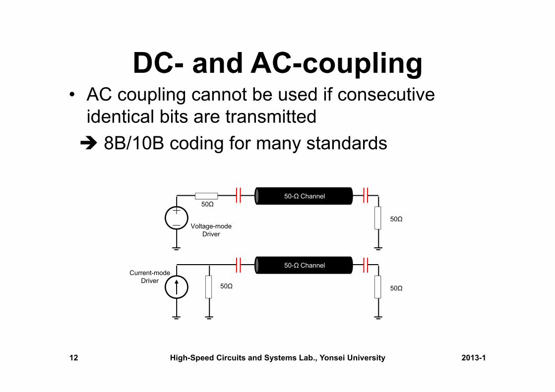
DC- and AC-coupling• AC coupling cannot be used if consecutive
identical bits are transmitted 8B/10B coding for many standards
2013-1High-Speed Circuits and Systems Lab., Yonsei University12
50Ω50-Ω Channel
50ΩVoltage-mode
Driver
50Ω
50-Ω Channel
50Ω
Current-modeDriver

Push-pull driver• 2 current sources
– Current path switching– Upper and lower pairs– Same rising and falling time
for each differential signal– Upper PMOS pair can be
replaced by NMOS pair to enhance switching time
– Head room problem in low-voltage technologies
– Used in Low-Voltage Differential Signals (LVDS) standard
– TX termination?
2013-1High-Speed Circuits and Systems Lab., Yonsei University13
Ibias
Positive channel
Negative channel
100Ω
IN- IN+
IN- IN+

CML (Current-Mode Logic) driver
• Loaded by 50ohm resistor– Current steering– Both side are terminated by 50Ω– Output voltage can be
both DC, AC-coupled– Used in most high-performance
serial link
2013-1High-Speed Circuits and Systems Lab., Yonsei University14
VDD
VSS
IN+ IN-
Ibias
50Ω 50Ω
Positive channel
Negative channel 100Ω

TX equalization• Channel causes ISI on received signal.
– High-frequency loss in channel eye-diagram closed
2013-1High-Speed Circuits and Systems Lab., Yonsei University15
TxDriver Channel Rx
Sampler

TX equalization• TX driver can be also channel equalizer
– TX driver can enhance high-frequency components before traveling through channel.
2013-1High-Speed Circuits and Systems Lab., Yonsei University16
TxDriver Channel Rx
Sampler

How to reject ISI?• FIR filtering
– Forcing cursors to 0 can be implemented by FIR filtering.– ISI can be removed since we know input data in TX-side– Tx-side FIR filtering can include pre-cursor
2013-1High-Speed Circuits and Systems Lab., Yonsei University17
1-bitPeriodDelay
InputData
(Digital)
+-- -
C-1 C1 C2
1-bitPeriodDelay
1-bitPeriodDelay
Subtractpre-cursor Main cursor
Subtract1st post-cursor
Subtract2nd post-cursor
OutputData
D-1 D1 D2
C0
D0
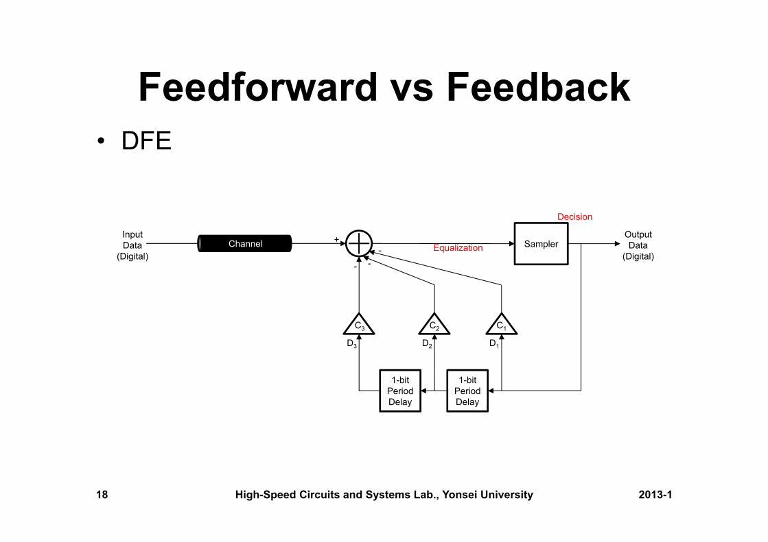
Feedforward vs Feedback• DFE
2013-1High-Speed Circuits and Systems Lab., Yonsei University18
InputData
(Digital)
+
- --
C1C2
1-bitPeriodDelay
1-bitPeriodDelay
C3
Channel Sampler
Decision
EqualizationOutputData
(Digital)
D1D2D3

Pre-/De-Emphasis– Tx FIR is often called Pre-/De-Emphasis
• De-emphasis: to reduce low-frequency components• Pre-emphasis: to enhance high-frequency components
– High-frequency component is transition bits
2013-1High-Speed Circuits and Systems Lab., Yonsei University19
NormalWaveform
De-emphasisWaveform
Pre-emphasisWaveform
Nominalswing
Nominal swing
Nominalswing

Circuit implementation• Current-mode drivers can be easily used for pre-
/de-emphasis– It is very easy to modify drivers into current-mode adder
including controllable gain
2013-1High-Speed Circuits and Systems Lab., Yonsei University20
D1- D1+
C1
Positive channel
Negative channel 100Ω
VSS
D0+ D0-
C0
50Ω 50Ω
VDD
Main cursor 1st post-cursor

Circuit implementation• Simultaneous implementation of pre-/de-emphasis
– D1=D0 Vout,diff = +/-50 x (C0-C1) De-emphasis– D1≠D0 Vout,diff = +/-50 x (C0+C1) Pre-emphasis– Level difference is defined as sum and subtract
2013-1High-Speed Circuits and Systems Lab., Yonsei University21
D1- D1+
C1
Positive channel
Negative channel 100Ω
VSS
D0+ D0-
C0
50Ω 50Ω
VDD
Main cursor 1st post-cursor
50x(C0+C1)50x(C0-C1)
-50x(C0-C1)
-50x(C0+C1)

Tx- vs. Rx- equalization• Tx equalization
– Consumes large power– Enlarged output signal improves SNR at Rx side– Easy implementation
• Rx equalization– Relatively low power consumption– More complex implementation (especially DFE)– For best performance, LE and DFE combination
2013-1High-Speed Circuits and Systems Lab., Yonsei University22

Design example
2013-1High-Speed Circuits and Systems Lab., Yonsei University23
“4-Channel 3.2/6.4-Gbps Dual-rate Transmitter”김두호, 최우영
대한전자공학회논문지 20104ch transmitter with 1-tap pre-emphasis
Dual-rate (3.2/ 6.4 Gbps)130nm CMOS technology / COB package600mW dissipation @1.2V power supply

Design example
2013-1High-Speed Circuits and Systems Lab., Yonsei University24
• 4-channel transmitter sharing a clock generator– 2:1 serializer function is included in pre-emphasis circuit– Displayport application

Design example• Clock generator performance
– PLL jitter is main performance metric of transmitter evaluation.
2013-1High-Speed Circuits and Systems Lab., Yonsei University25
3.2Gb/s 6.4Gb/s

Design example• De-emphasis waveform
2013-1High-Speed Circuits and Systems Lab., Yonsei University26
Vswing=600mVdiff / De-emphasis=1/3 Vswing=600mVdiff / De-emphasis=1/2
Vswing=600mVdiff / De-emphasis=2/3 Vswing=600mVdiff / De-emphasis=1
3.2Gb/s

Design example• De-emphasis waveform
2013-1High-Speed Circuits and Systems Lab., Yonsei University27
Vswing=600mVdiff / De-emphasis=1/3 Vswing=600mVdiff / De-emphasis=1/2
Vswing=600mVdiff / De-emphasis=2/3 Vswing=600mVdiff / De-emphasis=1
6.4Gb/s