high-speed serial interface - yonseitera.yonsei.ac.kr/class/2013_1_2/lecture/lect16_cdr-3.pdf ·...
TRANSCRIPT

High-speed Serial Interface
Lect. 16 – Clock and Data Recovery 3
2013-1High-Speed Circuits and Systems Lab., Yonsei University1

CDR Design Example (권대현)• Clock and Data Recovery Circuits
– Transceiver• PLL vs. CDR
– High-speed CDR• Phase Detector• Charge Pump• Voltage Controlled Oscillator
– Design target & Considerations
– Layout
– Post-layout simulation
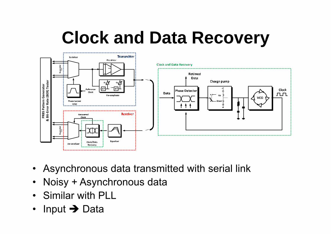
Clock and Data Recovery
• Asynchronous data transmitted with serial link• Noisy + Asynchronous data • Similar with PLL• Input Data
PRBS
Pat
tern
Gen
erat
or&
Bit-
Erro
r Rat
e (B
ER) T
este
r
N-p
aral
lel …
N-p
aral
lel …
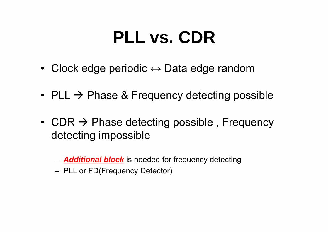
PLL vs. CDR• Clock edge periodic ↔ Data edge random
• PLL Phase & Frequency detecting possible
• CDR Phase detecting possible , Frequency detecting impossible
– Additional block is needed for frequency detecting– PLL or FD(Frequency Detector)
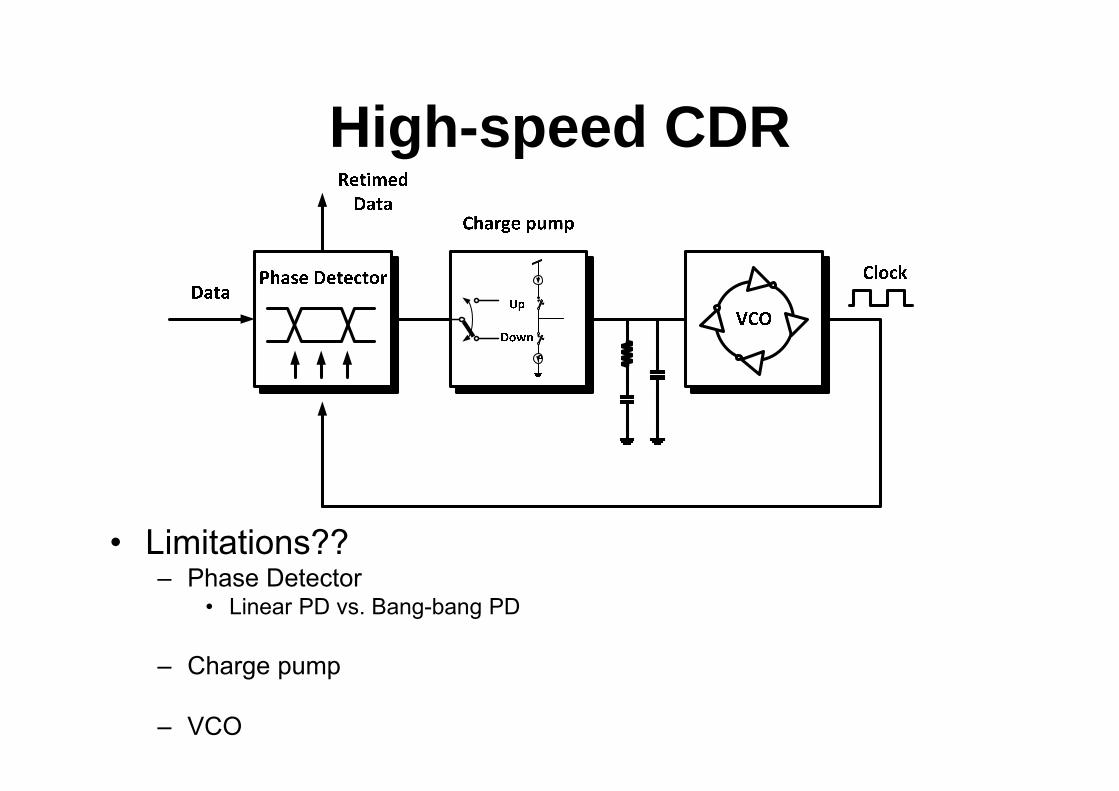
High-speed CDR
• Limitations??– Phase Detector
• Linear PD vs. Bang-bang PD
– Charge pump
– VCO
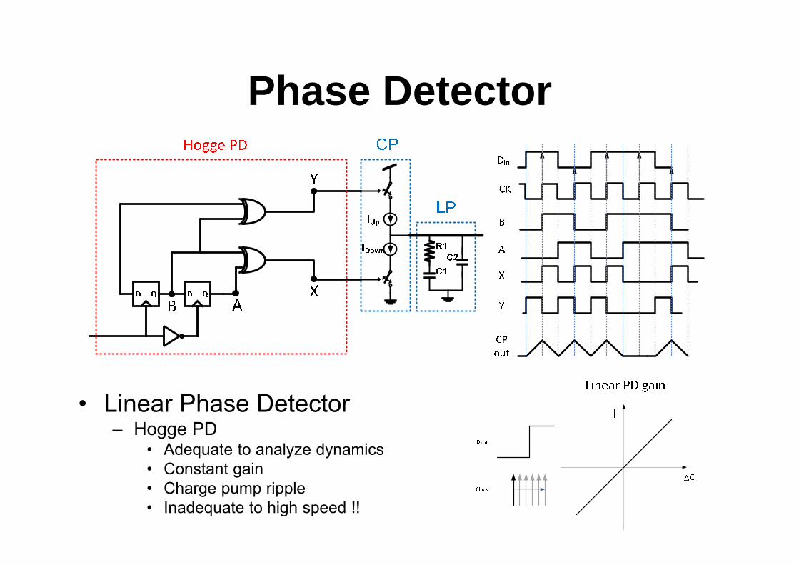
Phase Detector
• Linear Phase Detector– Hogge PD
• Adequate to analyze dynamics• Constant gain• Charge pump ripple• Inadequate to high speed !!
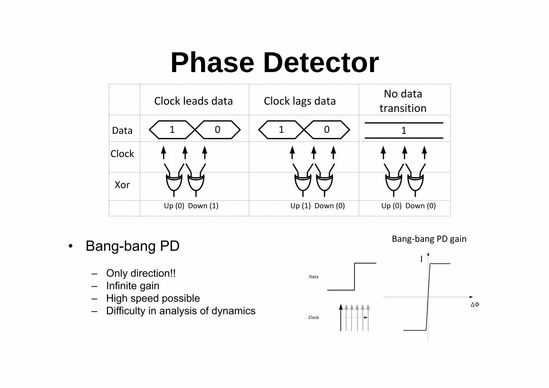
Phase Detector
• Bang-bang PD
– Only direction!!– Infinite gain– High speed possible– Difficulty in analysis of dynamics
1 0
Up (0) Down (1) Up (1) Down (0)
Data
Clock
Xor
1
Up (0) Down (0)
Clock leads data Clock lags data No data transition
1 0
Δɸ
I
Bang-bang PD gain
Data
Clock
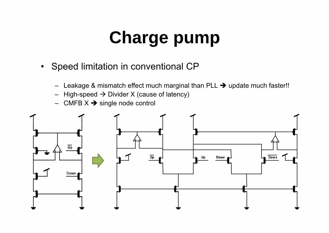
Charge pump• Speed limitation in conventional CP
– Leakage & mismatch effect much marginal than PLL update much faster!!– High-speed Divider X (cause of latency)– CMFB X single node control
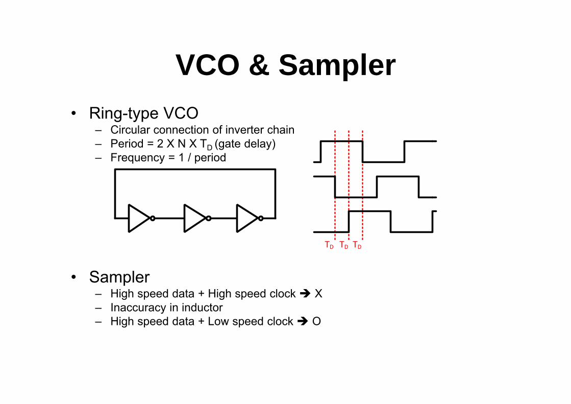
VCO & Sampler• Ring-type VCO
– Circular connection of inverter chain– Period = 2 X N X TD (gate delay)– Frequency = 1 / period
• Sampler– High speed data + High speed clock X– Inaccuracy in inductor– High speed data + Low speed clock O
TD TD TD

Multiphase clock CDR
Full-rate clock
Half-rate clock
Quarter-rate clock
• Quarter-rate sampling
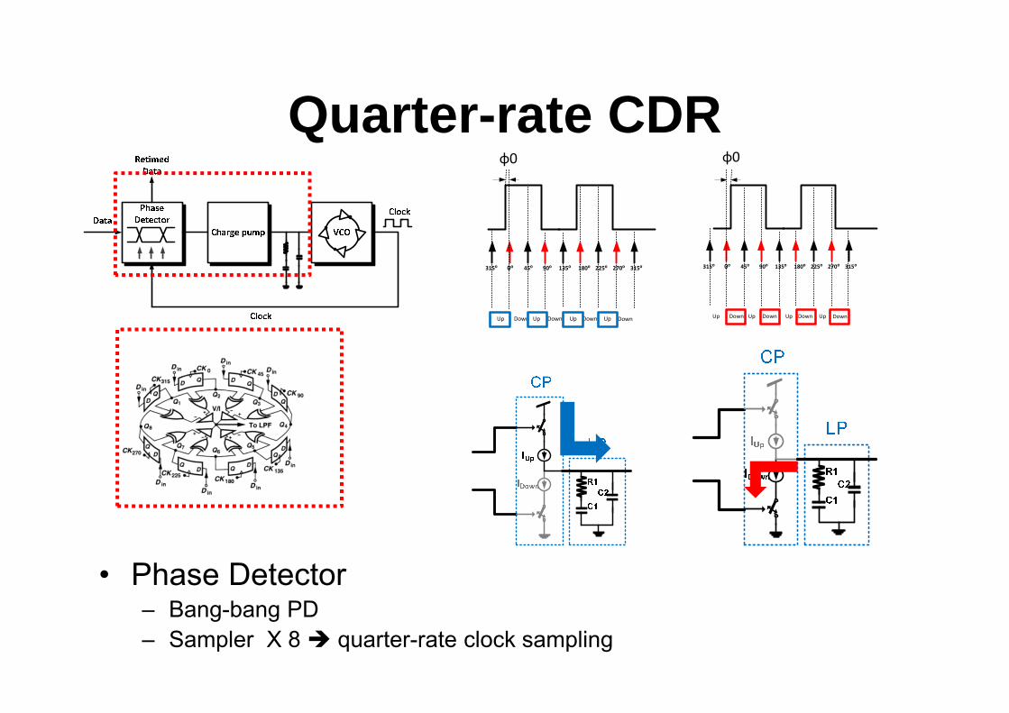
Quarter-rate CDR
• Phase Detector– Bang-bang PD– Sampler X 8 quarter-rate clock sampling
0⁰ 45⁰ 90⁰ 135⁰ 180⁰ 225⁰ 270⁰ 315⁰
Up Down Up Down Up Down Up Down
315⁰
ɸ0
0⁰ 45⁰ 90⁰ 135⁰ 180⁰ 225⁰ 270⁰ 315⁰
Up Down Up Down Up Down Up Down
315⁰
ɸ0
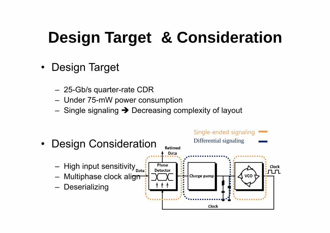
Design Target & Consideration
• Design Target
– 25-Gb/s quarter-rate CDR– Under 75-mW power consumption– Single signaling Decreasing complexity of layout
• Design Consideration
– High input sensitivity– Multiphase clock align– Deserializing
Single-ended signalingDifferential signaling

Layout• Design spec.
– 25-Gb/s quarter-rate CDR– 40 [ mW ] power consumption– Chip size
• Core size : 200 X 160 [um2]• Output Driver: 100 X 160 [um2]
200
um
160 um10
0 um
160 um
100
um
160 um
Mux_ref inp gnd inn Mux
sel01
Bff_ref
CP_ref
fine
contn
VDD
core
VDD
bff
ESD
VDD
VDD
vco
VDD
bff
coarse
VDD
core
gnd
Redp Redn gnd VDDvco clknclkp
MuxSel00
Input Data ( 25 Gb/s)
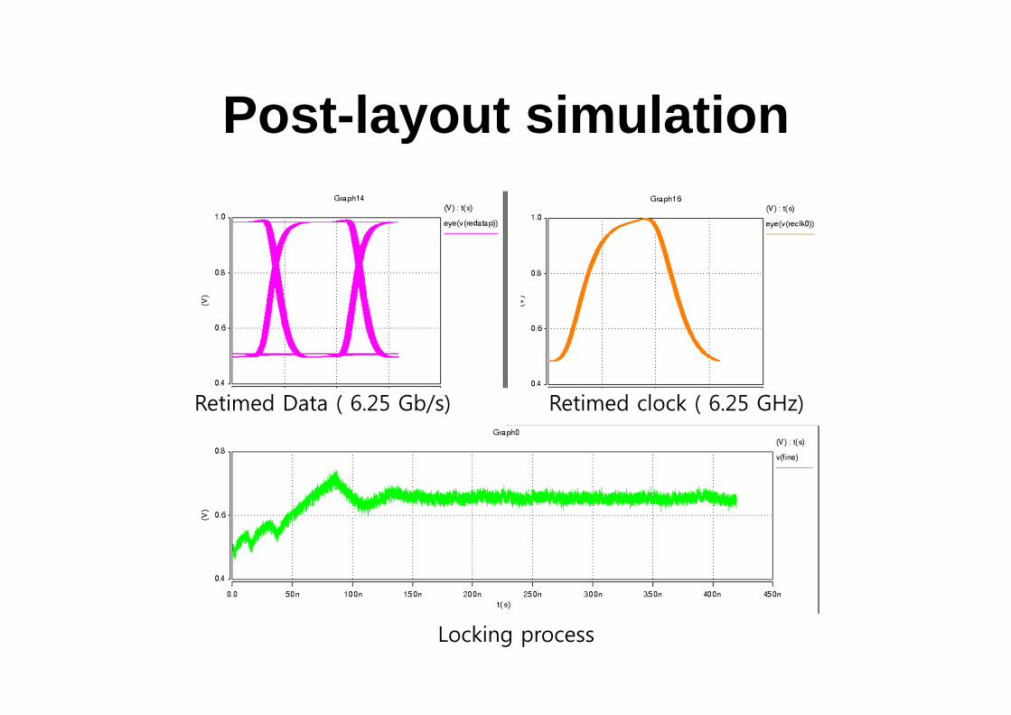
Post-layout simulation
Retimed Data ( 6.25 Gb/s) Retimed clock ( 6.25 GHz)
Locking process
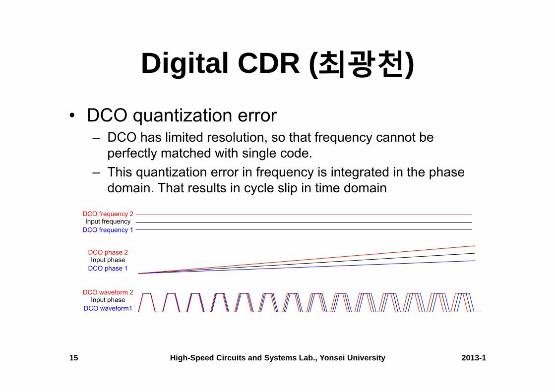
Digital CDR (최광천)• DCO quantization error
– DCO has limited resolution, so that frequency cannot be perfectly matched with single code.
– This quantization error in frequency is integrated in the phase domain. That results in cycle slip in time domain
2013-1High-Speed Circuits and Systems Lab., Yonsei University15
Input frequencyDCO frequency 2
DCO frequency 1
Input phaseDCO phase 2
DCO phase 1
Input phaseDCO waveform 2
DCO waveform1
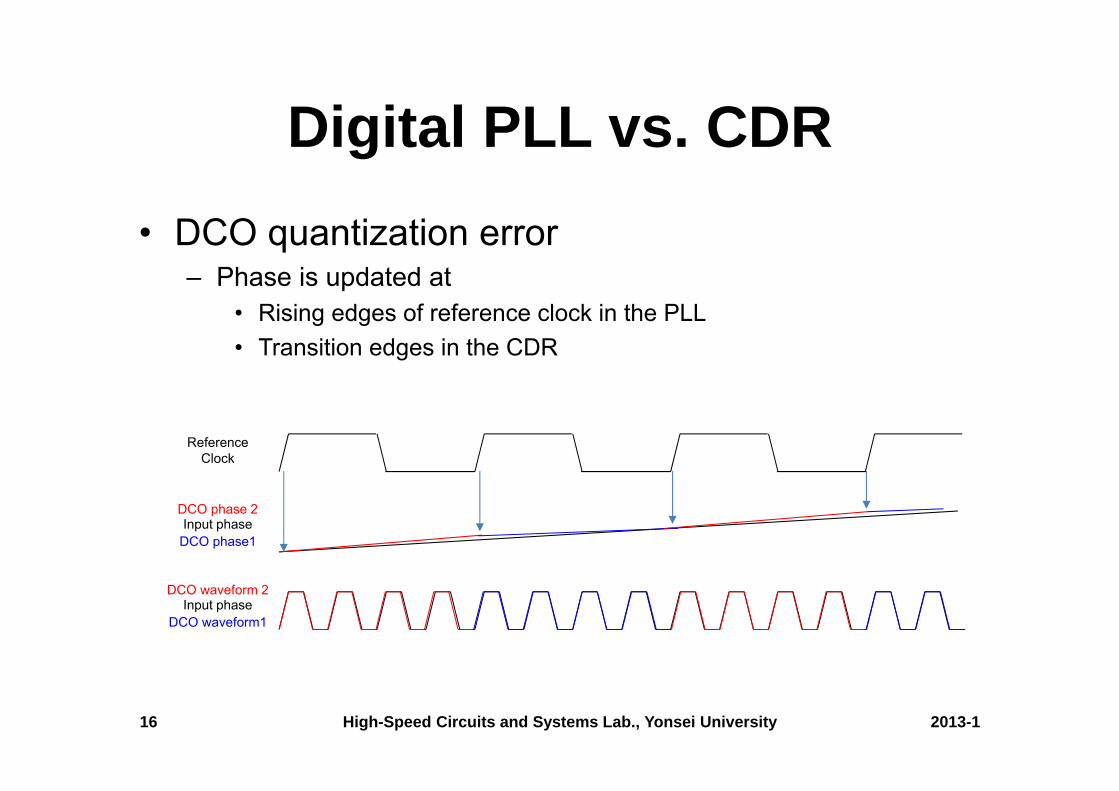
Digital PLL vs. CDR• DCO quantization error
– Phase is updated at• Rising edges of reference clock in the PLL • Transition edges in the CDR
2013-1High-Speed Circuits and Systems Lab., Yonsei University16
Input phaseDCO phase 2
DCO phase1
Input phaseDCO waveform 2
DCO waveform1
ReferenceClock
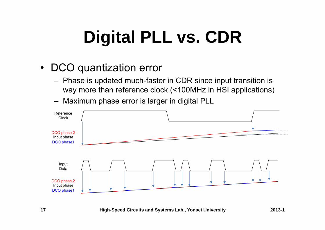
Digital PLL vs. CDR• DCO quantization error
– Phase is updated much-faster in CDR since input transition is way more than reference clock (<100MHz in HSI applications)
– Maximum phase error is larger in digital PLL
2013-1High-Speed Circuits and Systems Lab., Yonsei University17
Input phaseDCO phase 2
DCO phase1
ReferenceClock
Input phaseDCO phase 2
DCO phase1
InputData
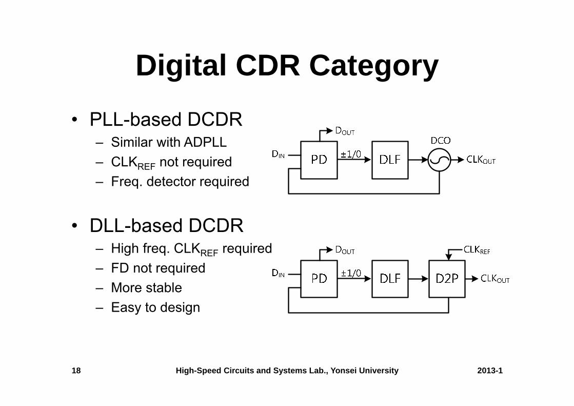
Digital CDR Category• PLL-based DCDR
– Similar with ADPLL– CLKREF not required– Freq. detector required
• DLL-based DCDR– High freq. CLKREF required– FD not required– More stable– Easy to design
2013-1High-Speed Circuits and Systems Lab., Yonsei University18
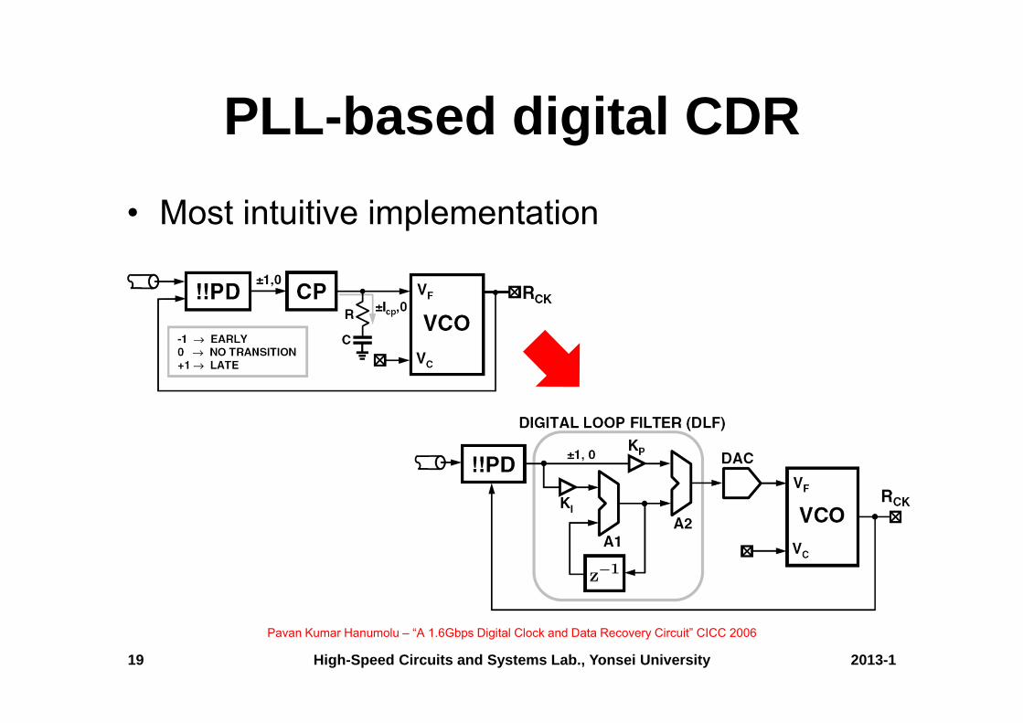
PLL-based digital CDR• Most intuitive implementation
2013-1High-Speed Circuits and Systems Lab., Yonsei University19
Pavan Kumar Hanumolu – “A 1.6Gbps Digital Clock and Data Recovery Circuit” CICC 2006

PLL-based digital CDR• Linearized model
– Z-domain model can be transformed into S-domain model as ADPLL.
– DCO part is analogous so that it cannot be perfectly modeled.
2013-1High-Speed Circuits and Systems Lab., Yonsei University20
Pavan Kumar Hanumolu – “A 1.6Gbps Digital Clock and Data Recovery Circuit” CICC 2006
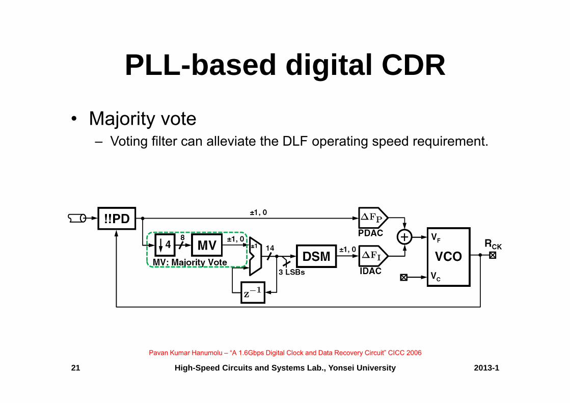
PLL-based digital CDR
2013-1High-Speed Circuits and Systems Lab., Yonsei University21
• Majority vote– Voting filter can alleviate the DLF operating speed requirement.
Pavan Kumar Hanumolu – “A 1.6Gbps Digital Clock and Data Recovery Circuit” CICC 2006
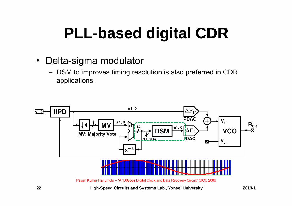
PLL-based digital CDR
2013-1High-Speed Circuits and Systems Lab., Yonsei University22
• Delta-sigma modulator– DSM to improves timing resolution is also preferred in CDR
applications.
Pavan Kumar Hanumolu – “A 1.6Gbps Digital Clock and Data Recovery Circuit” CICC 2006

DLL-based digital CDR
2013-1High-Speed Circuits and Systems Lab., Yonsei University23
• Digital to phase converter– Previously shown DLL-based phase controller is employed
Jeff L. Sonntag – “A Digital Clock and Data Recovery Architecture for Multi-Gigabit/s Binary Links” JSSC 2006
!!PD Voting filter DLF D2P

DLL-based digital CDR
2013-1High-Speed Circuits and Systems Lab., Yonsei University24
• Easily analyzed with z-domain model– Digital-to-phase converter is well-defined phase output, thus,
very good to model real situation.
Jeff L. Sonntag – “A Digital Clock and Data Recovery Architecture for Multi-Gigabit/s Binary Links” JSSC 2006
Linear PD
2013-1High-Speed Circuits and Systems Lab., Yonsei University25
• Bang-bang phase detector is much more appropriate for digital loop filter.– Bang-bang PD provides binary output.– Phase detection is possible even after deserialized.
• It is hard to give up linear dynamics.– Linear dynamics provides predictable bandwidth and stability.– But TDC used in digital PLL is not applicable in digital CDRs
because reference period is much smaller in CDR applications.
• How to digitize linear PD??
Digitizing linear PD
2013-1High-Speed Circuits and Systems Lab., Yonsei University26
Michael H. Perrott – “A 2.5-Gb/s Multi-Rate 0.25-m CMOS Clock and Data Recovery Circuit Utilizing a Hybrid Analog/Digital Loop Filter and All-Digital Referenceless Frequency Acquisition” JSSC 2006
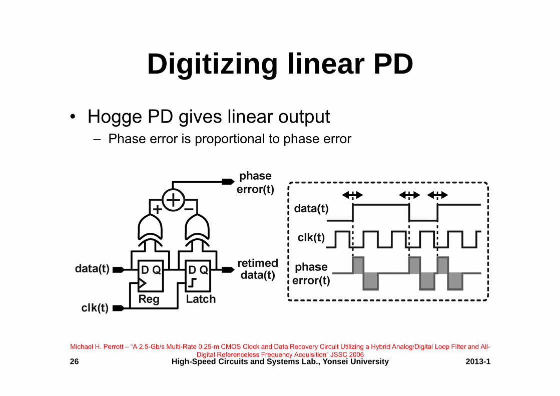
• Hogge PD gives linear output– Phase error is proportional to phase error
Digitizing linear PD
2013-1High-Speed Circuits and Systems Lab., Yonsei University27
Michael H. Perrott – “A 2.5-Gb/s Multi-Rate 0.25-m CMOS Clock and Data Recovery Circuit Utilizing a Hybrid Analog/Digital Loop Filter and All-Digital Referenceless Frequency Acquisition” JSSC 2006
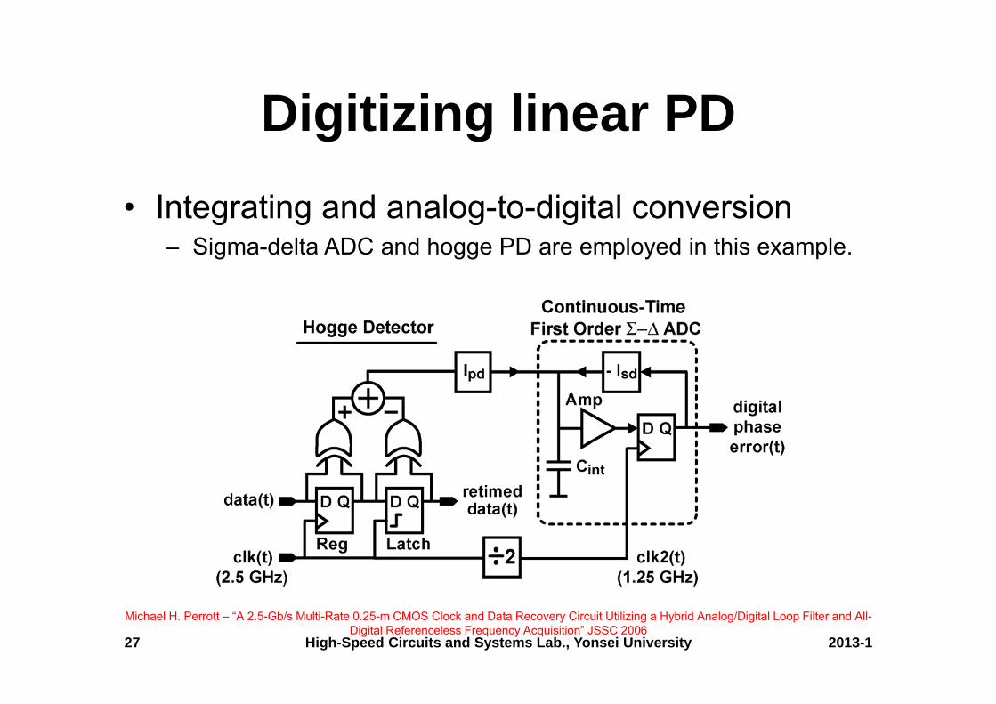
• Integrating and analog-to-digital conversion– Sigma-delta ADC and hogge PD are employed in this example.
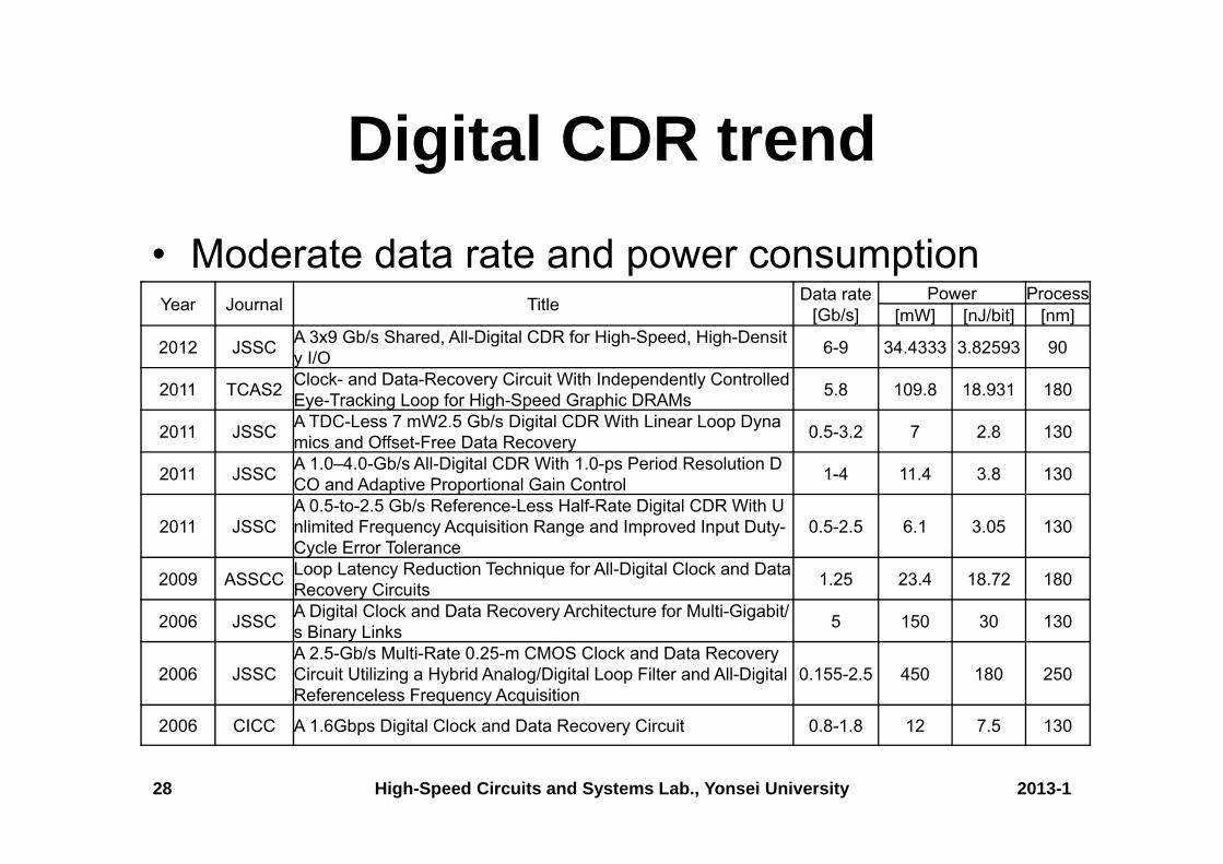
Digital CDR trend
2013-1High-Speed Circuits and Systems Lab., Yonsei University28
• Moderate data rate and power consumptionYear Journal Title Data rate
[Gb/s]Power Process
[mW] [nJ/bit] [nm]
2012 JSSC A 3x9 Gb/s Shared, All-Digital CDR for High-Speed, High-Density I/O 6-9 34.4333 3.82593 90
2011 TCAS2 Clock- and Data-Recovery Circuit With Independently Controlled Eye-Tracking Loop for High-Speed Graphic DRAMs 5.8 109.8 18.931 180
2011 JSSC A TDC-Less 7 mW2.5 Gb/s Digital CDR With Linear Loop Dynamics and Offset-Free Data Recovery 0.5-3.2 7 2.8 130
2011 JSSC A 1.0–4.0-Gb/s All-Digital CDR With 1.0-ps Period Resolution DCO and Adaptive Proportional Gain Control 1-4 11.4 3.8 130
2011 JSSCA 0.5-to-2.5 Gb/s Reference-Less Half-Rate Digital CDR With Unlimited Frequency Acquisition Range and Improved Input Duty-Cycle Error Tolerance
0.5-2.5 6.1 3.05 130
2009 ASSCC Loop Latency Reduction Technique for All-Digital Clock and Data Recovery Circuits 1.25 23.4 18.72 180
2006 JSSC A Digital Clock and Data Recovery Architecture for Multi-Gigabit/s Binary Links 5 150 30 130
2006 JSSCA 2.5-Gb/s Multi-Rate 0.25-m CMOS Clock and Data Recovery Circuit Utilizing a Hybrid Analog/Digital Loop Filter and All-Digital Referenceless Frequency Acquisition
0.155-2.5 450 180 250
2006 CICC A 1.6Gbps Digital Clock and Data Recovery Circuit 0.8-1.8 12 7.5 130