high voltage engineering (lucas)
TRANSCRIPT

8/6/2019 High Voltage Engineering (Lucas)
http://slidepdf.com/reader/full/high-voltage-engineering-lucas 1/212
+ + L L J J K K 9 9 R R O O W W D D J J H H
( ( Q Q J J L L Q Q H H H H U U L L Q Q J J
Senior Professor in Electrical Engineering
BScEng, MSc, PhD, FIEE, CEng, FIE(SL), MCS(SL)
2001
'HSDUWPHQW RI (OHFWULFDO (QJLQ8QLYHUVLW\ RI 0RUDWXZD 6UL

8/6/2019 High Voltage Engineering (Lucas)
http://slidepdf.com/reader/full/high-voltage-engineering-lucas 2/212
First Prod uced in Cyclostyled form 1970[Revised and Reprod uced p eriodically]
New Edition 1995Revised Edition 2001
Copyrigh t 2001 by J R Lucas
All rights reserved. No p art of this publication may be reprod uced or
transmitted in any form or by any means, electronic or mechanical,
including photocopy, recording, or any information storage and
retrieval system, without the w ritten permission from the Au thor.
Printed in Sri Lanka
8/6/2019 High Voltage Engineering (Lucas)
http://slidepdf.com/reader/full/high-voltage-engineering-lucas 3/212
i
Contents
1 BREAKDOWN OF GASEOUS INSULATION ............................................................................................................. 1
1.1 Ionisat ion of Gases ....................................................................................................................................................... 1
1.1.1 Ion isat ion p rocesses in gas d ischa rges............................................................................................................ 1
1.1.2 Relevan t gas ion isat ion p rocesses .................................................................................................................... 2
1.2 Breakdow n Characte rist ic in gases............................................................................................................................ 4
1.2.1 Electron Av alan che Mechan ism (Tow nsen d Breakdow n Process) ........................................................... 4
1.2.2 Paschen' s Law ..................................................................................................................................................... 7
1.2.3 Streamer M echan ism ....................................................................................................................................... 10
1.2.4 Factors a ffecting th e breakdow n v oltag e a Vacuu m gap .......................................................................... 10
1.2.5 Time lags of Spark breakdow n ...................................................................................................................... 13
1.2.6 Coron a Disch arges ........................................................................................................................................... 16
2 BREAKDOWN OF LIQUID AND SOLID INSULATION ....................................................................................... 22
2.1 Breakdow n in Liqu id s ............................................................................................................................................... 22
2.1.1 Breakdow n of Com mercia l liqu ids ............................................................................................................... 22
2.1.2 Breakd ow n due to gaseous inclusion s ......................................................................................................... 23
2.1.3 Brea kd ow n du e to liquid g lobu les ................................................................................................................ 232.1.4 Breakdow n du e to solid p ar ticles .................................................................................................................. 24
2.1.5 Pu rification of a liqu id for t estin g .................................................................................................................. 25
2.2 Breakdow n of Solid Insu lat ing Mater ials ............................................................................................................... 25
2.2.1 Electro-mechan ical breakd ow n...................................................................................................................... 25
2.2.2 Brea kd ow n du e to interna l d ischarge........................................................................................................... 26
2.2.3 Surface Breakdow n .......................................................................................................................................... 28
2.2.4 Therm al Breakd ow n ........................................................................................................................................ 29
2.2.5 Electro-chemical Break dow n.......................................................................................................................... 30
2.2.6 Chem ical Deterio ra tion ................................................................................................................................... 31
2.3 Breakdow n of Com posite Insu lat ion ...................................................................................................................... 32
3 LIGHTNING PHENOMENA ................ ................. ................ ................ ................ ................ ................ ................ ......... 34
3.1 Mech an ism of Ligh tn ing ........................................................................................................................................... 34
3.1.1 Breakdow n Process .......................................................................................................................................... 34
3.1.2 Fr equ ency of occurrence of ligh tn ing flash es .............................................................................................. 36
3.2 Ligh tn ing Problem for Transmission Lines ........................................................................................................... 36
3.2.1 Shield ing by overh ead grou nd w ires ........................................................................................................... 37
3.2.2 Calcu lat ion of Shield ing ang le ....................................................................................................................... 38
3.3 Area of attr action of transm ission sy stem s to ligh tnin g ...................................................................................... 40
3.4 Effects of Ligh tn ing on a Tran sm ission Line ......................................................................................................... 41
3.4.1 Strok es to a Phase-cond uctor .......................................................................................................................... 41

8/6/2019 High Voltage Engineering (Lucas)
http://slidepdf.com/reader/full/high-voltage-engineering-lucas 4/212
ii
3.4.2 Strok es to a tow er with no earth w ire ........................................................................................................... 41
3.4.3 Strok es to Earth wire ........................................................................................................................................ 42
3.4.4 Strok es to nearby objects (Ind irect Strok es) ................................................................................................. 43
4 HIGH VOLTAGE TRANSIENT ANALYSIS ............................................................................................................... 45
4.1 Surges on Tran sm ission Lines .................................................................................................................................... 45
4.1.1 Surge Imp ed an ce an d Velocity of Propagatio n........................................................................................... 47
4.1.2 Energy stored in surge..................................................................................................................................... 49
4.2 Reflection of Travel ling waves at a Junction .......................................................................................................... 49
4.2.1 Op en circu ited lin e fed from a infin ite source ............................................................................................. 50
4.2.2 Shor t Circuit Line fed from a n infin ite sou rce ............................................................................................. 51
4.3 Bewley Lattice Diagram ............................................................................................................................................ 52
4.3.1 Analysis of an open-circu it lin efed from ideal source ............................................................................... 53
4.3.2 Reflections at 3 substa tion system ................................................................................................................. 55
4.4 Reflection an d Transmission at a T-junction .......................................................................................................... 584.5 Berger on 's Metho d of Gra phica l Solut ion .............................................................................................................. 59
4.6 Represen tation of Lump ed Elements in trave lling wave techniques ................................................................ 61
4.7 Bran ch Time Table for d igital com pu ter im plementa tion ................................................................................... 62
4.8 Transform Meth od s of solv ing Transien ts ............................................................................................................. 63
5 HIGH VOLTAGE CABLES ............... ................ ................ ................ ................. ................ ................ ................ .............. 64
5.0 High Voltage Cables .................................................................................................................................................. 64
5.1 Pow er loss in the Ca ble.............................................................................................................................................. 64
5.1.1 Dielectr ic loss..................................................................................................................................................... 65
5.1.2 Con ductor loss .................................................................................................................................................. 655.1.3 Shea th loss ......................................................................................................................................................... 65
5.1.4 Intersheath Loss ................................................................................................................................................ 65
5.1.5 Cross-bond ing of Cab les ................................................................................................................................. 66
5.2 Imp reg na ted Paper Insu lat ion ................................................................................................................................. 67
5.2.1 Properties requ ired of cable insu latio n ......................................................................................................... 68
5.2.2 Prin ciple un derlyin g the d esign of high volta ge cable insu lation ........................................................... 68
5.2.3 Paper insulated p ow er cables......................................................................................................................... 69
5.2.4 Insu lat ion Resistan ce ....................................................................................................................................... 69
5.2.5 Cap acita nce in a single-core cable............................................................................................................... 70
5.2.6 Thr ee-core Cables ............................................................................................................................................. 70
5.2.7 Thr ee-core belted ty pe Cables ........................................................................................................................ 71
5.2.8 Hochstad ter o r "H" typ e Cable....................................................................................................................... 73
5.2.9 S.L. typ e Cable................................................................................................................................................... 73
5.2.10 Copper Space Factor ....................................................................................................................................... 74
5.3 Dielectric Stress in a Sing le Core Cab le................................................................................................................... 75
5.3.1 Ca ble Grad ing for Un iform Stress Distribution .......................................................................................... 76
5.3.2 Cap acita nce Gr ad ing ....................................................................................................................................... 76
5.3.3 Intersheath Grad ing ......................................................................................................................................... 77
5.4 Pressu rised High Voltage Cables ............................................................................................................................. 79
5.4.1 Oil-p ressure cables ......................................................................................................................................... 79
5.4.2 Gas-pressu re cables ....................................................................................................................................... 81
8/6/2019 High Voltage Engineering (Lucas)
http://slidepdf.com/reader/full/high-voltage-engineering-lucas 5/212
iii
5.4.3 Externa l Pressu re Cab les .............................................................................................................................. 81
5.4.4 Intern al Pressu re Cables ............................................................................................................................... 81
5.5 Therm al Design of Cables ......................................................................................................................................... 83
5.5.1 Cu rren t ra ting of Cables .................................................................................................................................. 83
5.5.2 Therm al Resista nce .......................................................................................................................................... 84
5.5.3 Therm al Resistance of single-core cable ....................................................................................................... 85
5.5.4 Therm al resistan ce of three-core cables ........................................................................................................ 86
5.5.5 Therm al resistan ce of p rotectiv e coverin gs.................................................................................................. 86
5.5.6 Thermal resistance of grou nd ar ou nd cab le ................................................................................................ 86
5.5.7 Cab les exposed to a ir ....................................................................................................................................... 88
5.6 High Volta ge Bushings .............................................................................................................................................. 88
5.6.1 Simp le cylindrical bu sh ing ........................................................................................................................... 88
5.6.2 Con denser bush ing .......................................................................................................................................... 89
6 MEASUREMENT OF HIGH VOLTAGES .................................................................................................................... 91
6.0 High Voltag e Mea su rem ent...................................................................................................................................... 91
6.1 Direct Mea surement of High Voltages ................................................................................................................... 91
6.1.1 Electrosta tic Voltm eters ................................................................................................................................... 91
6.1.2 Sph ere gaps ....................................................................................................................................................... 92
6.2 Tran sform er and p oten tial divid er meth od s of measu rem ent ........................................................................... 95
6.2.1 Transform er rat io meth od .............................................................................................................................. 95
6.2.2 Resist ive potent ial d ivid er meth od ............................................................................................................. 96
6.2.3 Capacitiv e potent ial d ivid er meth od ............................................................................................................ 97
6.2.4 Matching of Potent ial div iders........................................................................................................................ 986.3 Mea surement of Surges ............................................................................................................................................ 105
6.3.1 Klyd onograph .................................................................................................................................................. 105
6.4 Gen era l measurem ents ............................................................................................................................................. 107
6.4.1 Pea k read ing voltm eter s................................................................................................................................. 107
6.4.2 Oscilloscope for measurem ent of fast tran sien ts........................................................................................ 110
6.5 Mea surements of cap acita nce an d loss tan gen t ................................................................................................... 110
6.5.1 High Volta ge Scherin g Bridge....................................................................................................................... 110
6.5.2 Dielectric loss measurem ent using Oscilloscop e ....................................................................................... 112
6.5.3 D etection of interna l d ischa rges ................................................................................................................... 116
6.5.4 Measu remen t of dielectric constant an d d issipation factor of a liquid d ielectric at high usin g a
freq uencies reson an ce meth od ................................................................................................................... 119
6.5.5 Ionic Win d Voltmeter ................................................................................................................................... 122
6.5.6 Du mb-bell Voltm eter .................................................................................................................................... 122
7 HIGH VOLTAGE GENERATORS FOR TESTING .................................................................................................. 123
7.0 Gen era tion of High Voltages ................................................................................................................................... 123
7.1 Gen era tion of High Alte rn ating Voltages ............................................................................................................. 123
7.1.1 Cascad e ar rang em ent of tran sformers ......................................................................................................... 123
7.1.2 Reson an t Tran sformers .................................................................................................................................. 124
7.1.3 High freq uency high voltages ....................................................................................................................... 125
7.2 Gen era tion of High Direct Voltages ....................................................................................................................... 128

8/6/2019 High Voltage Engineering (Lucas)
http://slidepdf.com/reader/full/high-voltage-engineering-lucas 6/212
iv
7.2.1 Rectifier circu its ............................................................................................................................................... 128
7.2.2 Voltage Multip lier Cir cuit s ............................................................................................................................ 128
7.2.3 Electrosta tic generator s................................................................................................................................... 130
8 HIGH VOLTAGE SURGE GENERATORS ................................................................................................................ 132
8.0 High Voltage Imp ulse Gen era tors .......................................................................................................................... 132
8.1 Imp ulse Waveform .................................................................................................................................................... 133
8.1.1 Single exp onential w aveform ........................................................................................................................ 133
8.1.2 D ou ble exponent ial waveform ...................................................................................................................... 133
8.1.3 Calculation of . an d from resistance an d capacitan ce valu es.............................................................. 135
8.1.4 Definition of Wavefron t and Wavetail tim es of pr actical w avefor ms.................................................... 136
8.1.5 A va lid a pp roximate ana lysis of dou ble expon ential im pu lse genera tor circuit ................................. 137
8.1.6 Wavefront and Wa vetail Con tro l ................................................................................................................. 138
8.2 Op era tion of Imp ulse Gen era tor ............................................................................................................................. 139
8.2.1 Un contro lled op era tion .................................................................................................................................. 1398.2.2 Con tro lled op era tion ....................................................................................................................................... 140
8.2.3 Trigatr on gap .................................................................................................................................................... 141
8.3 Mu lti-sta ge Imp ulse Gen era tors ............................................................................................................................. 142
8.3.1 Marx Imp ulse Genera tor Circuit ................................................................................................................... 142
8.3.2 Good let Impulse Gen era tor Circu it .............................................................................................................. 143
8.3.3 Simulta neous brea kd ow n of successive sph ere gap s................................................................................ 143
8.3.4 Genera tion of chop ped imp ulse wavefor ms .............................................................................................. 147
9 HIGH VOLTAGE TESTING ................ ................ ................ ................ ................ ................ ................ ................ ........... 148
9.0 High Volta ge Testin g Pro ced ure ............................................................................................................................. 1489.1 General tests carr ied o ut o n H igh v oltage equ ipm ent ........................................................................................ 148
9.1.1 Sustain ed low-frequency tests ....................................................................................................................... 149
9.1.2 High Volta ge dir ect curr en t tests .................................................................................................................. 149
9.1.3 High -frequency test s ....................................................................................................................................... 149
9.1.4 Surge or impulse t ests ..................................................................................................................................... 150
9.2 Testin g of solid dielectric mate ria ls ........................................................................................................................ 151
9.2.1 N atu re of d ielectr ic break dow n .................................................................................................................... 151
9.2.2 Deter min ation of d ielectric st ren gth of solid d ielectrics ........................................................................... 152
9.3 Imp ulse Test ing .......................................................................................................................................................... 153
9.4 Voltage Distribution in a Transform er Win ding .................................................................................................. 155
9.5 Tests on Insu lators ..................................................................................................................................................... 158
9.5.1 Typ e test s .......................................................................................................................................................... 158
9.5.2 Sample Tests ..................................................................................................................................................... 159
9.5.3 Rou tine Tests .................................................................................................................................................... 159
9.6 Tests on Transform ers .............................................................................................................................................. 160
9.7 Tests on Cables ........................................................................................................................................................... 161
9.7.1 Tests on Pr essu rised Cables ........................................................................................................................... 162
9.8 Tests on High Voltage Bushing s ............................................................................................................................. 163
9.8.1 Bush ing ............................................................................................................................................................. 163
9.8.2 Tests on Bush ings ............................................................................................................................................ 163
9.9 Tests on Porcelain and tou ghened glass insu lators for over hea d pow er lines ............................................... 164

8/6/2019 High Voltage Engineering (Lucas)
http://slidepdf.com/reader/full/high-voltage-engineering-lucas 7/212
v
10 INSULATION CO-ORDIN ATION ............... ................ ................ ................ ................ ................ ................ ................ 166
10.0 Insu lat ion Co-ord ina tion .......................................................................................................................................... 166
10.1 Term ino logy ............................................................................................................................................................... 166
10.2 Conv ent iona l metho d of insu lation co-ord inat ion .............................................................................................. 168
10.3 Stat istical Metho d of Insu lat ion Co-or d inatio n .................................................................................................... 169
10.3.1 Evaluatio n o f Risk Factor ............................................................................................................................. 170
10.4 Length of Ov erh ead Shield ing Wire ...................................................................................................................... 170
10.4.1 Mod ification of Wavesha pe by Corona ..................................................................................................... 171
10.5 Surge Protection ......................................................................................................................................................... 173
10.5.1 Spark gaps for surge pro tection .................................................................................................................. 173
10.5.2 Surge Diverters .............................................................................................................................................. 174
10.5.3 Selection of Surge Diver ter s......................................................................................................................... 176
10.5.4 Separation limit for ligh tn ing ar restor s ..................................................................................................... 178
11 HIGH VOLTAGE DIRECT CURRENT TRAN SMISSION ..................................................................................... 184
11.0 Historical Background .............................................................................................................................................. 184
11.1 Com parison of a.c an d d .c tra nsmission ................................................................................................................ 185
11.1.1 Ad vantages of d .c.......................................................................................................................................... 185
11.1.2 Inherent problem s asso ciated with hv dc .................................................................................................. 188
11.1.3 Econo mic Compar ison ................................................................................................................................. 189
11.2 Conver tor ar rangem ents an d op era tion ................................................................................................................ 190
11.2.1 Con trol an gle (Delay an gle)......................................................................................................................... 191
11.2.2 Com mutation ang le (overlap an gle) .......................................................................................................... 191
11.2.3 Curren t Waveform s ...................................................................................................................................... 19511.2.4 Power factor cos 3 ............... ................. ................ ................ ................ ................ ................ ................ ........ 196
11.2.5 Curren t waveforms on a.c. system ............................................................................................................. 197
11.2.6 Inversion ......................................................................................................................................................... 198
11.3 Con tro l Characterist ics ............................................................................................................................................. 199
11.3.1 Na tura l Voltage Char acteristic (NV) and the Con stant Ignition An gle (CIA) control ..................... 199
11.3.2 Con stant Extinction An gle (CEA) contro l ................................................................................................ 199
11.3.3 Con stant Cu rren t Contro l (CC)................................................................................................................... 200
11.3.4 Full Ch aracterist ic of Con ver tor .................................................................................................................. 200
11.3.5 Com pou nd ing o f Convertors....................................................................................................................... 201
11.3.6 Per U nit Con ver tor Chart............................................................................................................................. 202
11.4 Classificatio n of d .c. lin ks ......................................................................................................................................... 203
11.4.1 Harmon ics an d Filters ................................................................................................................................... 204
INDEX .............. ................. ................ ................ ................ ................ ................ ................ ................ ............... ................ ............ 205

8/6/2019 High Voltage Engineering (Lucas)
http://slidepdf.com/reader/full/high-voltage-engineering-lucas 8/212
vi
!701,.0
This book has arisen out of the need to include many of the major aspects of high voltage engineering in a single volum e. The book is intend ed prim arily asa basic text book in high voltage engineering at the Final Year level of a four
year undergraduate course specialising in Electrical Engineering, withemp hasis on heavy curren t engineering. It is also expected to be of imm ensevalue to practising electrical engineers, especially to those in the electricitysupply industry.
The substance of this book is organised in th e following major sections. (i)Review of breakdown of insulating materials, (ii) Surge phenomena and theiranalysis, (iii) Generation of high voltages for testing purposes, (iv)measurem ent of high voltages and testing p rocedur e, and (v) Co-ordination of insulation in a p ower system.
A prior knowledge of basic electrical engineering theory and electric powersystem analysis has been considered as a pre-requisite in writing this book.However, important background material is reviewed as a refresher whereever considered n ecessary.
Information for this book has been collated over a p eriod of over 25 years fromvarious sources, a record of which has not been maintained, during theteaching of high voltage engineering as a subject to electrical engineeringun dergrad uates at the University of Moratuwa and its pred ecessors. Theauthor is grateful to each of these sources, but regrets his inability to thank them ind ividu ally.
This book, althou gh it h as not come ou t as a comp lete text book before the 1995edition, it has nevertheless come out in parts, mainly as lecture handouts overthe p eriod of time. In fact, the original comp lete edition in cyclostyled formcame out during the period July-September 1971 and has undergonecontinuous revisions.
October 2001 J. R. Lucas
8/6/2019 High Voltage Engineering (Lucas)
http://slidepdf.com/reader/full/high-voltage-engineering-lucas 9/212
%UHDNGRZQ RI*DVHRXV ,QVXODWLRQ
1.1 Ionisation of Gases
Electrical Insulating Materials (or Dielectrics) are materials in which electrostatic fields can remain almostindefinitely. These materials thus offer a very high resistance to the passage of direct currents. However,they cannot withstand an infinitely high voltage. When the applied voltage across the dielectric exceeds acritical value the insulation will be damaged. The dielectrics may be gaseous, liquid or solid in form.
Gaseous dielectrics in practice are not free of electrically charged particles, including free electrons. Theelectrons, which may be caused by irradiation or field emission, can lead to a breakdown process to beinitiated. These free electrons, however produced, on the application of an electric field are acceleratedfrom the cathode to the anode by the electric stress applying a force on them. They acquire a kineticenergy (½ mu 2) as they move through the field. The energy is usually expressed as a voltage (in electron-volt, eV, where e is the charge on an electron) as the energies involved are extremely small. [The energyEi = e V i is expressed in electron volt. 1 e V = 1.6 x 10 -19 J]. These free electrons, moving towards theanode collide with the gas molecules present between the electrodes. In these collisions, part of thekinetic energy of the electrons is lost and part is transmitted to the neutral molecule. If this molecule gainssufficient energy (more than the energy E i necessary for ionisation to occur), it may ionise by collision.
The (mean) number of ionising collisions by one electron per unit drift across the gap is not a constant butsubject to statistical fluctuations. The newly liberated electron and the impinging electron are thenaccelerated in the field and an electron avalanche is set up. Further increase in voltage results inadditional ionising processes. Ionisation increases rapidly with voltage once these secondary processestake place, until ultimately breakdown occurs.
It is worth noting that in uniform fields, the ionisation present at voltages below breakdown is normally toosmall to affect engineering applications. In non-uniform fields, however, considerable ionisation may bepresent in the region of high stress, at voltages well below breakdown, constituting the well known coronadischarge.
1.1.1 Ionisation processes in gas discharges
The electrical breakdown of a gas is brought about by various processes of ionisation. These are gasprocesses involving the collision of electrons, ions and photons with gas molecules, and electrodeprocesses which take place at or near the electrode surface [Electrons can be emitted from the cathode if the stress is around 100 - 1000 kV/cm due to field emission].
Ionisation is the process by which an electron is removed from an atom, leaving the atom with a nettpositive charge (positive ion). Since an electron in the outermost orbit is subject to the least attractiveforce from the nucleus, it is the easiest removed by any of the collision processes. The energy required toremove an outer electron completely from its normal state in the atom to a distance well beyond thenucleus is called the first ionisation potential.
The reciprocal process of an electron falling from a great distance to the lowest unoccupied orbit is alsopossible. In this case, a photon will be emitted having the same energy as previously absorbed.

8/6/2019 High Voltage Engineering (Lucas)
http://slidepdf.com/reader/full/high-voltage-engineering-lucas 10/212
High Voltage Engineering - J R L UCAS , 20012
1.1.2 Relevant gas ionisation processes
(i) Ionisation by simple collision
When the kinetic energy of an electron (½ mu²), in collision with a neutral gas molecule exceeds theionisation energy (E i = e V i) of the molecule, then ionisation can occur.(i.e. when ½ mu² > E i)
M + e - (½ mu²) →M+ + 2 e -
In general, a positive ion and 2 slow moving electrons will result. The probability of this process is zerofor electron energies equal to the ionisation energy E i, but increases almost linearly at first, and thengradually with electron energy up to a maximum.
When the gas molecules are bombarded with electrons, other electrons bound to atoms may be freed bythe collision with the high energy electron. The ratio of the electrons given by collision to the primaryelectrons depend, mainly on the energy of the primaries. This is maximum at primary electron energies of about 200 - 500 eV. For lower energy values, the energy transferred may not be sufficient to causeelectrons to escape from the surface of the molecules, and thus the probability of ionisation is small. Formuch higher values of primary energies, the energy of the impinging electron would be sufficient for thiselectron to penetrate the surface deeper into the molecule, so that again the chance of escape of otherelectrons decreases.
Thus the variation of the ionisation probability in air with increase of electron energy is as shown in figure1.1.
Figure 1.1 - Ionisation probability curve in air
(ii) Excitation
In the case of simple collision, the neutral gas molecule does not always gets ionised on electron impact.In such cases, the molecule will be left in an excited state M *, with energy E e.
M + e - (½ mu²) → M* + e -
This excited molecule can subsequently give out a photon of frequency v with energy emitted h v. Theenergy is given out when the electron jumps from one orbit to the next.
M* → M + h v
where h = Planck's constant = 6.624 x 10 -34 J s
00 1 0 0 2 0 0 3 0 0 4 0 0 5 0 0 6 0 0
e lec t ron en e rg y ( eV )
i o n i s a t i o n
p r o b a b i
8/6/2019 High Voltage Engineering (Lucas)
http://slidepdf.com/reader/full/high-voltage-engineering-lucas 11/212
Breakdown of Gaseous Insulation
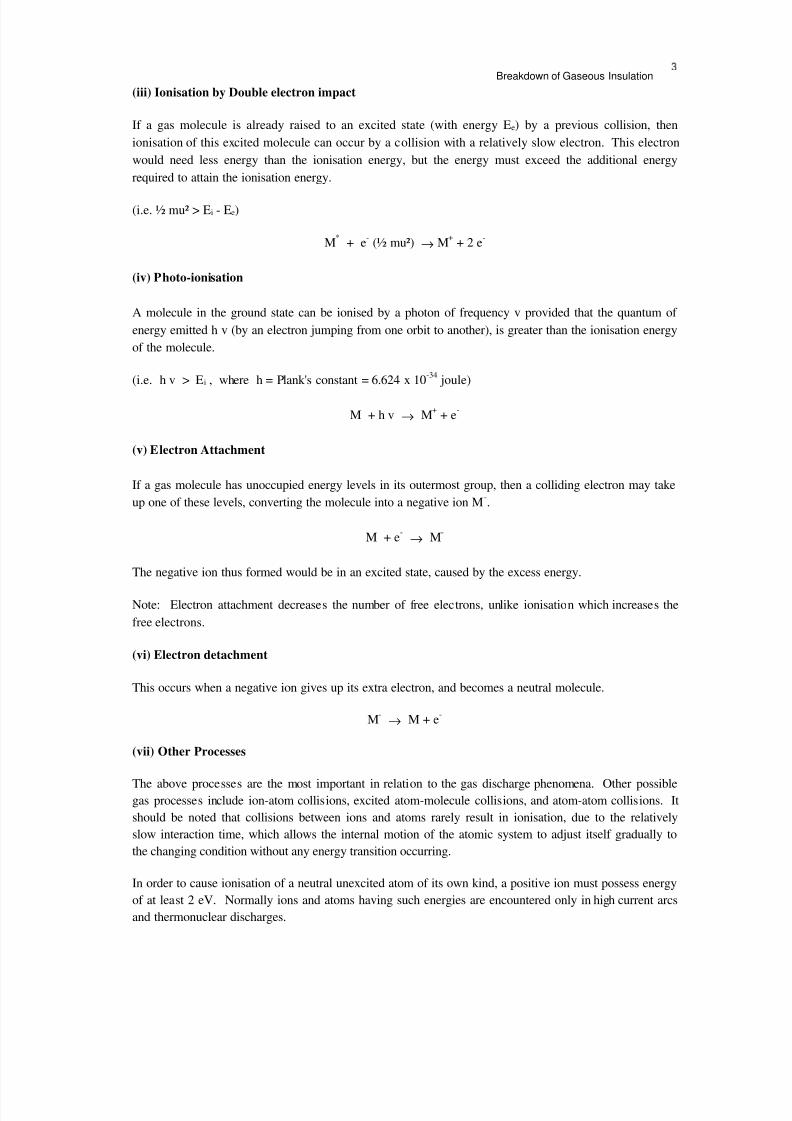
(iii) Ionisation by Double electron impact
If a gas molecule is already raised to an excited state (with energy E e) by a previous collision, thenionisation of this excited molecule can occur by a collision with a relatively slow electron. This electronwould need less energy than the ionisation energy, but the energy must exceed the additional energyrequired to attain the ionisation energy.
(i.e. ½ mu² > E i - E e)
M* + e - (½ mu²) →M+ + 2 e -
(iv) Photo-ionisation
A molecule in the ground state can be ionised by a photon of frequency v provided that the quantum of energy emitted h v (by an electron jumping from one orbit to another), is greater than the ionisation energy
of the molecule.
(i.e. h v > E i , where h = Plank's constant = 6.624 x 10 -34 joule)
M + h v → M+ + e -
(v) Electron Attachment
If a gas molecule has unoccupied energy levels in its outermost group, then a colliding electron may takeup one of these levels, converting the molecule into a negative ion M -.
M + e - → M-
The negative ion thus formed would be in an excited state, caused by the excess energy.
Note: Electron attachment decreases the number of free electrons, unlike ionisation which increases thefree electrons.
(vi) Electron detachment
This occurs when a negative ion gives up its extra electron, and becomes a neutral molecule.
M- → M + e -
(vii) Other Processes
The above processes are the most important in relation to the gas discharge phenomena. Other possiblegas processes include ion-atom collisions, excited atom-molecule collisions, and atom-atom collisions. Itshould be noted that collisions between ions and atoms rarely result in ionisation, due to the relativelyslow interaction time, which allows the internal motion of the atomic system to adjust itself gradually tothe changing condition without any energy transition occurring.
In order to cause ionisation of a neutral unexcited atom of its own kind, a positive ion must possess energyof at least 2 eV. Normally ions and atoms having such energies are encountered only in high current arcsand thermonuclear discharges.
8/6/2019 High Voltage Engineering (Lucas)
http://slidepdf.com/reader/full/high-voltage-engineering-lucas 12/212
High Voltage Engineering - J R L UCAS , 20014
1.2 Breakdown Characteristic in gases
Two mechanisms of breakdown in gasses is known. These are the avalanche and streamer mechanisms.
1.2.1 Electron Avalanche Mechanism (Townsend Breakdown Process)
One of the processes which are considered in breakdown is the Townsend breakdown mechanism. It isbased on the generation of successive secondary avalanches to produce breakdown.
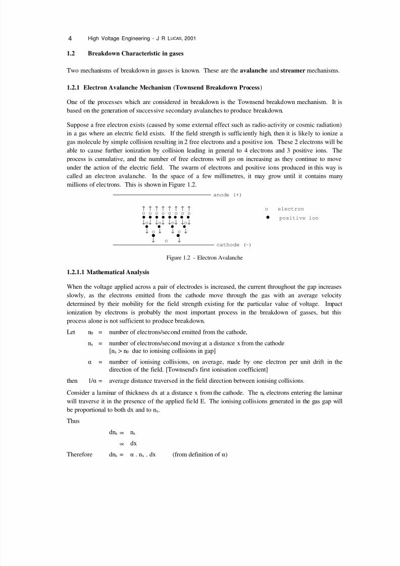
Suppose a free electron exists (caused by some external effect such as radio-activity or cosmic radiation)in a gas where an electric field exists. If the field strength is sufficiently high, then it is likely to ionize agas molecule by simple collision resulting in 2 free electrons and a positive ion. These 2 electrons will beable to cause further ionization by collision leading in general to 4 electrons and 3 positive ions. Theprocess is cumulative, and the number of free electrons will go on increasing as they continue to moveunder the action of the electric field. The swarm of electrons and positive ions produced in this way is
called an electron avalanche. In the space of a few millimetres, it may grow until it contains manymillions of electrons. This is shown in Figure 1.2.
1.2.1.1 Mathematical Analysis
When the voltage applied across a pair of electrodes is increased, the current throughout the gap increasesslowly, as the electrons emitted from the cathode move through the gas with an average velocitydetermined by their mobility for the field strength existing for the particular value of voltage. Impactionization by electrons is probably the most important process in the breakdown of gasses, but thisprocess alone is not sufficient to produce breakdown.
Let n 0 = number of electrons/second emitted from the cathode,
nx = number of electrons/second moving at a distance x from the cathode[nx > n0 due to ionising collisions in gap]
. = number of ionising collisions, on average, made by one electron per unit drift in thedirection of the field. [Townsend's first ionisation coefficient]
then 1/ . = average distance traversed in the field direction between ionising collisions.
Consider a laminar of thickness dx at a distance x from the cathode. The n x electrons entering the laminarwill traverse it in the presence of the applied field E. The ionising collisions generated in the gas gap willbe proportional to both dx and to n x.
Thus
dnx ∝ nx
∝ dx
Therefore dn x = . . nx . dx (from definition of . )
FFFFFFFFFFFFFFFFFFFFFFFFFFFFFFDQRG e (+)
↑ ↑ ↑ ↑ ↑ ↑ ↑ ↑ o electrono o o o o o o oz z z z z z z z z positive ion↓o ↓ ↓o ↓ ↓o ↓ ↓o ↓
z z z z ↓ o ↓ ↓ o ↓
z z ↓ o ↓
FFFFFFFFFFFFFFFFFFFFFFFFFFFFFFFFDWKRGH -)
Figure 1.2 - Electron Avalanche

8/6/2019 High Voltage Engineering (Lucas)
http://slidepdf.com/reader/full/high-voltage-engineering-lucas 13/212
Breakdown of Gaseous Insulation
Rearranging and integrating gives
If the anode is at a distance x = d from the cathode, then the number of electrons n d striking the anodeper second is given by
nd = n0 . e. d
Therefore, on the average, each electron leaving the cathode produces (n d - n0)/n0 new electrons (andcorresponding positive ions) in the gap.
In the steady state , the number of positive ions arriving at the cathode/second must be exactly equal to
the number of newly formed electrons arriving at the anode. Thus the circuit current will be given by
I = I 0 . e. d
where I 0 is the initial photo-electric current at the cathode.
In the actual breakdown process, the electron impact ionization is attended by secondary processes on thecathode, which replenish the gas gap with free electrons, with every newly formed avalanche surpassingthe preceding one in the number of electrons.
Consider now the current growth equations with the secondary mechanism also present.
Let = number of secondary electrons (on average) produced at the cathode per ionising collision inthe gap. [Townsend's second ionisation coefficient]
n0 = number of primary photo-electrons/second emitted from the cathoden0' = number of secondary electrons/second produced at the cathoden0" = total number of electrons/second leaving the cathode
Then n 0' = n 0 + n0"
On the average, each electron leaving the cathode produces [e. d - 1] collisions in the gap, giving the
number of ionising collisions/second in the gap as n 0" (e. d - 1). Thus by definition
e.n=n
x.=)n / n(
dx=nnd
x0 x
0 xe
x
0 x
xn
n
x
0
α
α
α
log
∫ ∫
)1-e(-1n ="n
resultthegivesThis
.)1-e("n+n="n thatson+n="n but
)1-e("n=n giving
d0
0
d000
000
d00
α
α
α
γ
γ
γ
′
′
)1-e("nn =
d 0
0α
γ '′

8/6/2019 High Voltage Engineering (Lucas)
http://slidepdf.com/reader/full/high-voltage-engineering-lucas 14/212
High Voltage Engineering - J R L UCAS , 20016
Similar to the case of the primary process (with . only), we have
Thus, in steady state, the circuit current I will be given by
This equation describes the growth of average current in the gap before spark breakdown occurs.
As the applied voltage increases, e. d and e
. d increase until e. d →1 , when the denominator of the
circuit current expression becomes zero and the current I → ∞ . In this case, the current will, in practice,be limited only by the resistance of the power supply and the conducting gas.
This condition may thus be defined as the breakdown and can be written as
(e. d - 1) = 1
This condition is known as the Townsend criteria for spark breakdown .
The avalanche breakdown develops over relatively long periods of time, typically over 1 s and does notgenerally occur with impulse voltages.
1.2.1.2 Determination of Townsend's Coefficients . and
Townsend's coefficients are determined in an ionisation chamber which is first evacuated to a very highvacuum of the order of 10 -4 and 10 -6 torr before filling with the desired gas at a pressure of a few torr.The applied direct voltage is about 2 to 10 kV, and the electrode system consists of a plane high voltageelectrode and a low voltage electrode surrounded by a guard electrode to maintain a uniform field. Thelow voltage electrode is earthed through an electrometer amplifier capable of measuring currents in therange 0.01 pA to 10 nA. The cathode is irradiated using an ultra-violet lamp from the outside to producethe initiation electron. The voltage current characteristics are then obtained for different gap settings. Atlow voltage the current growth is not steady. Afterwards the steady Townsend process develops as shownin figure 1.3.
From the Townsend mechanism, the discharge current is given by
)1-e(-1en =e"n=n d
d 0d
0d α
α α
γ
)1-e(-1e I = I d
d 0
α
α
γ
discharge ¿ self sustaining dischargescurrent I G- - - - - - - - - - - - - - - - - - - - - - - G← breakdown
G QRQ -self sustained dischargesG G G G G G G G G G- - - - - I G G G G G JFFFFFFFFFFFFFFFFFFFFFFFFFFFFFFFFFFFOFFFFFFFFFOFFFFFFFFF¾
Vo V1 V2 voltage V
)LJXUH 7\SLFDO &XUUHQW JURZWK
1»d when α γ
α α
α
e I )1-e(-1
e I = I d 0d
d 0 ≈

8/6/2019 High Voltage Engineering (Lucas)
http://slidepdf.com/reader/full/high-voltage-engineering-lucas 15/212
Breakdown of Gaseous Insulation
This can be written in logarithmic form as
ln I = . d + ln I 0
y = m x + c
From a graph of ln I vs d, the constants . and I 0 can be determined from the gradient and the interceptrespectively, as in figure 1.4.
Once I 0 and . are known, can be determined from points on the upward region of the curve. Theexperiment can be repeated at different pressures if required.
1.2.1.3 Breakdown in electronegative gases
In the above analysis, electron attachment to neutral molecules was not considered. Electron attachmentremoves free electrons and thus gives gases very high dielectric strengths. The gases in which electron
attachment occurs are electro-negative gases.
An attachment coefficient can be defined, analogous with . , as the number of attachments per electronper unit drift in the direction of the field. Under these conditions, the equation for the average currentgrowth in a uniform field can be shown to be as follows.
The corresponding criteria for spark breakdown is
1.2.2 Paschen's Law
When electrons and ions move through a gas in a uniform field E and gas pressure p, their mean energiesattain equilibrium values dependant on the ratio E/p; or more precisely
. /p = f 1(E/p) and = f 2(E/p)
¿ ln I G
G G G G G G G G
ln I o G G G G JFFFFFFFFFFFFFFFFFFFFFFFFOFFFFFFFFFFFFFF¾
gap spacing d
)LJXUH 9DULDWLRQ RI OQ , YV G
[ ]1-e -
-1
- -e
- I = I
d )-(
d )-(
0ηα
ηα
ηα α γ
ηα η
ηα α
1=-e -
1
d )-( ηα
ηα α γ

8/6/2019 High Voltage Engineering (Lucas)
http://slidepdf.com/reader/full/high-voltage-engineering-lucas 16/212
High Voltage Engineering - J R L UCAS , 20018
For a uniform field gap, the electric field E = V/d. Thus applying Townsend's criterion for spark breakdown of gases gives
which may be written in terms of the functions as
This equation shows that the breakdown voltage V is an implicit function of the product of gas pressure pand the electrode separation d.
That is V = f (p.d)
In the above derivation the effect of temperature on the breakdown voltage is not taken into account.Using the gas equation pressure . volume = mass . R . absolute Temperature , we see that pressure =density . R . absolute Temperature . Thus the correct statement of the above expression is V =f( G ZKHUH! LV WKH JDV GHQVLW\ 7KLV LV WKH VWDWHPHQW RIPaschen's Law .
Under constant atmospheric conditions, it is experimentally found that the breakdown voltage of a uniformfield gap may be expressed in the form
V = A . d + B . √d where d is the gap spacing
For air, under normal conditions, A = 24.4 kV/cm and B = 6.29 kV/cm1/2.
[The breakdown voltage gradient is about 30 kV/cm in uniform fields for small gaps of the order of 1 cm,but reduces to about 6 kV/cm for large gaps of several meters]
Figure 1.5 shows a typical breakdown vs spacing characteristic.
This variation with spacing can be modified using Paschen's Law to include the variation with gas densityas follows.
where / = relative density (or gas density correction factor).
1=)1-e( d α γ
1=-ed p
V f 1
d p
V f d p
21
breakdown ¿ voltage (kV) G
G G G G G
G G G G JFFFFFFFFFFFFFFFFFFFFFFFFFFFFFFFFFFFFFFF¾
gap spacing d (cm)
Figure 1.5 - Breakdown characteristic
)d ( B+)d ( A=
)d (. B
+d . A
=V 0
1/20
21
21
δ δ
ρ ρ
ρ ρ
8/6/2019 High Voltage Engineering (Lucas)
http://slidepdf.com/reader/full/high-voltage-engineering-lucas 17/212
Breakdown of Gaseous Insulation
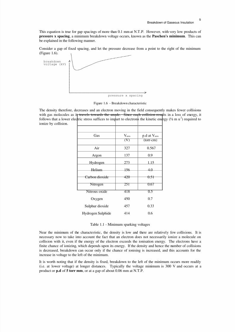
This equation is true for gap spacings of more than 0.1 mm at N.T.P. However, with very low products of pressure x spacing , a minimum breakdown voltage occurs, known as the Paschen's minimum . This canbe explained in the following manner.
Consider a gap of fixed spacing, and let the pressure decrease from a point to the right of the minimum(Figure 1.6).
The density therefore, decreases and an electron moving in the field consequently makes fewer collisionswith gas molecules as it travels towards the anode. Since each collision results in a loss of energy, itfollows that a lower electric stress suffices to impart to electrons the kinetic energy (½ m u 2) required toionize by collision.
Gas V min (V)
p.d at V min (torr-cm)
Air 327 0.567
Argon 137 0.9
Hydrogen 273 1.15
Helium 156 4.0
Carbon dioxide 420 0.51
Nitrogen 251 0.67
Nitrous oxide 418 0.5
Oxygen 450 0.7
Sulphur dioxide 457 0.33
Hydrogen Sulphide 414 0.6
Table 1.1 - Minimum sparking voltages
Near the minimum of the characteristic, the density is low and there are relatively few collisions. It isnecessary now to take into account the fact that an electron does not necessarily ionize a molecule oncollision with it, even if the energy of the electron exceeds the ionisation energy. The electrons have afinite chance of ionizing, which depends upon its energy. If the density and hence the number of collisionsis decreased, breakdown can occur only if the chance of ionising is increased, and this accounts for the
increase in voltage to the left of the minimum.It is worth noting that if the density is fixed, breakdown to the left of the minimum occurs more readily(i.e. at lower voltage) at longer distances. Typically the voltage minimum is 300 V and occurs at aproduct or p.d of 5 torr mm , or at a gap of about 0.06 mm at N.T.P.
breakdown ¿ voltage (kV) G
G G G G G G G G G JFFFFFFFFFFFFFFFFFFFFFFFFFFFFFFFFFFFFFFF¾
pressure x spacing
Figure 1.6 - Breakdown characteristic
8/6/2019 High Voltage Engineering (Lucas)
http://slidepdf.com/reader/full/high-voltage-engineering-lucas 18/212
High Voltage Engineering - J R L UCAS , 200110
At very low pressures, and at very high pressures (compared with atmospheric), Paschen's Law fails.Also, Paschen's Law is valid for temperatures below about 1100 0C. A further increase in temperatureultimately results in the failure of Paschen's Law because of thermal ionisation.
It can be seen from the breakdown characteristic, that for a constant gap spacing, the breakdown voltage,and hence the breakdown stress required, is very much higher than at atmospheric conditions, under veryhigh pressure and under very low pressures (high vacuum) conditions. Thus both high vacuum as well ashigh gas pressure can be used as insulating media. [The vacuum breakdown region is that in which thebreakdown voltage becomes independent of the gas pressure] Under normal conditions, operation is wellto the right of Paschen's minimum.
The table 1.1 gives the minimum sparking potential for various gases.
1.2.3 Streamer Mechanism
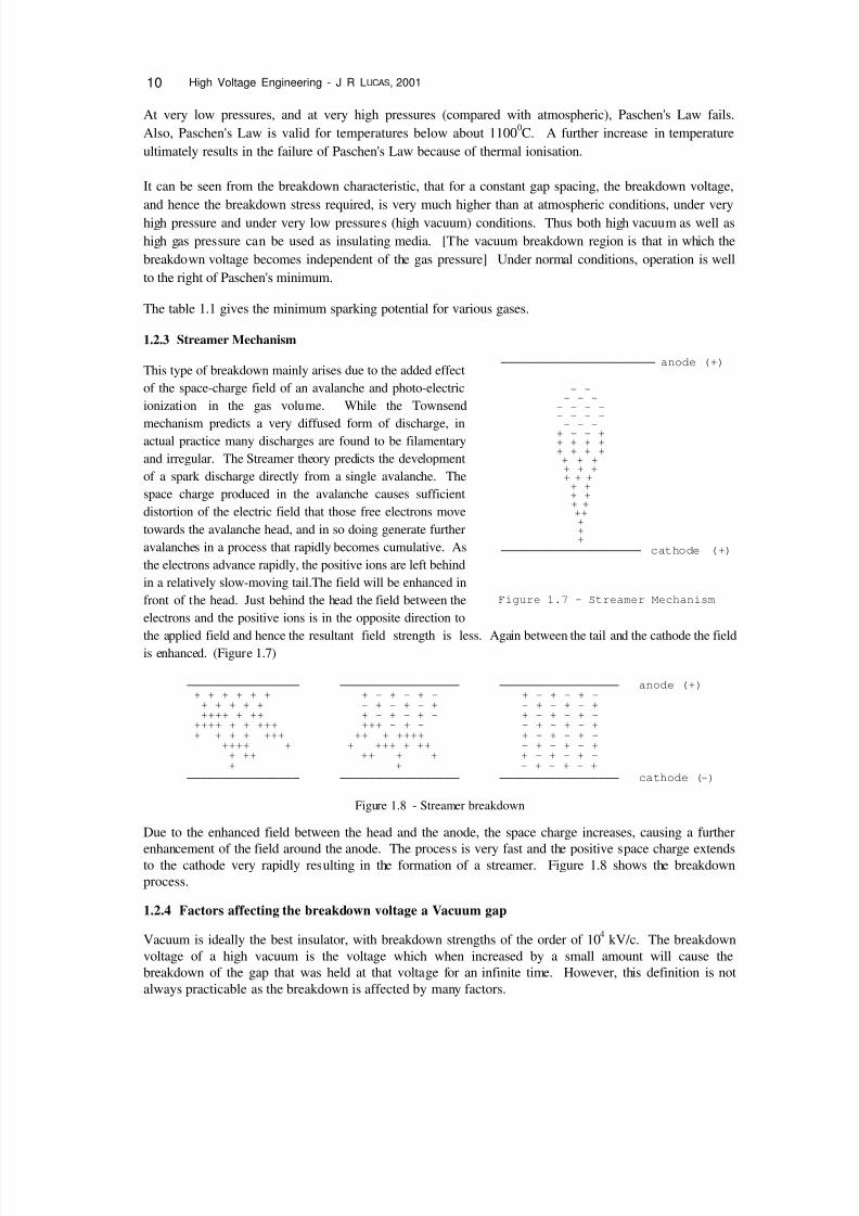
This type of breakdown mainly arises due to the added effectof the space-charge field of an avalanche and photo-electricionization in the gas volume. While the Townsendmechanism predicts a very diffused form of discharge, inactual practice many discharges are found to be filamentaryand irregular. The Streamer theory predicts the developmentof a spark discharge directly from a single avalanche. Thespace charge produced in the avalanche causes sufficientdistortion of the electric field that those free electrons movetowards the avalanche head, and in so doing generate furtheravalanches in a process that rapidly becomes cumulative. As
the electrons advance rapidly, the positive ions are left behindin a relatively slow-moving tail.The field will be enhanced infront of the head. Just behind the head the field between theelectrons and the positive ions is in the opposite direction tothe applied field and hence the resultant field strength is less. Again between the tail and the cathode the fieldis enhanced. (Figure 1.7)
Due to the enhanced field between the head and the anode, the space charge increases, causing a furtherenhancement of the field around the anode. The process is very fast and the positive space charge extendsto the cathode very rapidly resulting in the formation of a streamer. Figure 1.8 shows the breakdownprocess.
1.2.4 Factors affecting the breakdown voltage a Vacuum gap
Vacuum is ideally the best insulator, with breakdown strengths of the order of 10 4 kV/c. The breakdownvoltage of a high vacuum is the voltage which when increased by a small amount will cause thebreakdown of the gap that was held at that voltage for an infinite time. However, this definition is notalways practicable as the breakdown is affected by many factors.
FFFFFFFFFFFFFFFFFFFFFFDQRGH
- -- - -
- - - -- - - -
- - -+ - - ++ + + ++ + + +
+ + ++ + ++ + +
+ ++ ++ ++++++
FFFFFFFFFFFFFFFFFFFF FDWKRGH
Figure 1.7 - Streamer Mechanism
FFFFFFFFFFFFFFFF FFFFFFFFFFFFFFFFF FFFFFFFFFFFFFFFFF DQRGH + + + + + + + - + - + - + - + - + -
+ + + + + - + - + - + - + - + - +++++ + ++ + - + - + - + - + - + -
++++ + + +++ +++ - + - - + - + - ++ + + + +++ ++ + ++++ + - + - + -
++++ + + +++ + ++ - + - + - ++ ++ ++ + + + - + - + -+ + - + - + - +
FFFFFFFFFFFFFFFF FFFFFFFFFFFFFFFFF FFFFFFFFFFFFFFFFF FDWKRGH -)
Figure 1.8 - Streamer breakdown

8/6/2019 High Voltage Engineering (Lucas)
http://slidepdf.com/reader/full/high-voltage-engineering-lucas 19/212
Breakdown of Gaseous Insulation(i) Electrode Separation
For vacuum gaps less than about 1 mm, the breakdown voltage is approximately proportional to the length,all other parameters remaining constant. This gives a constant breakdown strength. For these small gaps,the breakdown stress is relatively high, being of the order of 1 MV/cm. Field emission of electronsprobably plays an important part in the breakdown process.
V = k . d for d < 1 mm
For gaps greater than about 1 mm, the breakdown voltage does not increase at an equal rate and theapparent breakdown stress for longer gaps is much reduced, being about 10 kV/cm at a spacing of 10 cm.[Apparent stress is defined as the voltage required to cause breakdown divided by the distance between
the electrodes]. Figure 1.9.
Cranberg has shown theoretically that for longer gaps, it is the product of breakdown voltage andbreakdown stress that remains constant.
V . E = k 1 for d > 1 mm.
where the constant k 1 depends on the material and surface conditions of the electrodes.
For an Uniform field gap , E = V/d, so that
V = k 2 d1/2
Or in a more general form, both regions can be expressed by the equation
V = k d x where x = 0.5 for long gaps > 1 mm= 1 for gaps < 1mm
(ii) Electrode Effects
Conditioning
The breakdown voltage of a gap increases on successive flashovers, until a constant value is reached.
The electrodes are then said to be conditioned. This increase in voltage is ascribed to the burning off bysparking of microscopic irregularities or impurities which may exist on the electrodes. When investigatingthe effect of various factors on breakdown, the electrodes must first be conditioned in such a way thatreproducible results are obtained.
breakdown ¿ breakdown voltage (kV) if causedG by field emission only
750 FM
G actual breakdownG voltage (kV)500 FM
G G
250 FM breakdown stressG kV/cm )G JFFFFFFFFPFFFFFFFFNFFFFFFFFNFFFFFFFFNFFF¾ 0 1 2 3 4
gap spacing (cm)
Figure 1.9 - Breakdown characteristic

8/6/2019 High Voltage Engineering (Lucas)
http://slidepdf.com/reader/full/high-voltage-engineering-lucas 20/212
High Voltage Engineering - J R L UCAS , 200112
The effect of conditioning is shown in figure 1.10. The breakdown voltage of conditioned electrodes or
gaps is very much reproducible than otherwise, and hence breakdown values that are normally obtainedexperimentally are those of conditioned electrodes. Unconditioned electrodes may have breakdownvalues a low as 50% of the breakdown voltage with conditioned electrodes.
(iii) Material and Surface Finish
Electrode Material Voltage across 1 mm gap(kV)
Steel 122
Stainless Steel 120Nickel 96
Monel metal 60
Aluminium 41
Copper 37
Table 1.2 - Effect of electrode material on breakdown
The electrode surfaces form the physical boundaries between which the breakdown finally takes place.Thus it is not surprising to find that the breakdown strength of a given size of gap is strongly dependant on
the material of the electrodes. In general, the smoother the surface finish, the greater the breakdownvoltage.
(iv) Surface contamination
Presence of contamination in the test cell reduces the breakdown voltage sometimes by as much as 50%of the clean electrode value.
(v) Area and configuration of electrodes
Increasing the area of the electrodes makes it more difficult to maintain a given breakdown voltage. Thusbreakdown voltage decreases slightly with increase in surface area. For example, electrodes of 20 cm 2 area gives the breakdown voltage across a 1 mm gap of 40 kV, whereas electrodes of the same material of area 1000 cm 2 gives a breakdown voltage across the same 1 mm gap as 25 kV.
breakdown ¿ voltage (kV) G
G x40 FM [ [ [ [ [ [ [ [ [
G [ [ [ G [ [ [ G [
30 FM [ xG [ [ G [ x x
20 FM[ G G G
10 FM G G G JFFFFFFFFNFFFFFFFFFNFFFFFFFFFNFFFFFFFFFNFFFFFFFF¾ number of the breakdown
0 5 10 15 20
Figure 1.10 - Breakdown characteristics

8/6/2019 High Voltage Engineering (Lucas)
http://slidepdf.com/reader/full/high-voltage-engineering-lucas 21/212
Breakdown of Gaseous InsulationUp to 1 mm gap, the more convex electrodes have higher breakdown voltage than the more nearly planeelectrodes even though at the same voltage they carried a higher electric field at the surface.
(vi) Temperature
The variation of the breakdown voltage with temperature is very small, and for nickel and iron electrodes,the strength remains unchanged for temperatures as high as 500 0C. Cooling the electrodes to liquidNitrogen temperature increases the breakdown voltage.
(vii) Frequency of applied voltage
It is known that a given gap stands a higher impulse voltage than an alternating voltage, and a higheralternating voltage than a direct voltage. However, it has been shown that for a small gap (2 mm) there isno dependence of the breakdown voltage on the frequency in the range 50 Hz to 50 kHz.
(viii) Vacuum Pressure
For small gaps, increasing the degree of vacuum increases the breakdown voltage until below a certainpressure there is no change. The vacuum breakdown region is the region in which the breakdown voltagebecomes independent of the nature of the pressure of the gap between the electrodes.
However, for large gaps (about 200 mm spacing) it is found that below a certain pressure the breakdownvoltage starts decreasing again, so that the breakdown stress at this stage could in fact be improved byactually worsening the vacuum.
For example, using a 1.6 mm diameter sphere opposite a plane cathode and a gap of 200 mm, thecharacteristics shown in figure 1.11 was obtained. The breakdown voltage was constant for pressure lessthan 5 x 10 - 4 torr, but rose with increasing pressure to a maximum at 5 x 10 - 4 torr, with further increasein pressure the voltage fell sharply.
1.2.5 Time lags of Spark breakdown
In practice, particularly in high voltage engineering, breakdown under impulse fields is of greatimportance. On the application of a voltage, a certain time elapses before actual breakdown occurs eventhough the applied voltage may be much more than sufficient to cause breakdown.
breakdown ¿ breakdown voltage (kV) if causedvoltage(kV) G E\ ILHOG HPLVVLRQ RQO\
1200 FM G
1000 FM G
800 FM G
600 FM G
400 FM G
200FM
G
0 JFFFFFFFFNFFFFFFFFNFFFFFFFFNFFFFFFFFNFFF¾ 10 -6 10 -5 10 -4 10 -3 10 -2
Pressure (torr)
Fi ure 1.11 - Breakdown characteristic

8/6/2019 High Voltage Engineering (Lucas)
http://slidepdf.com/reader/full/high-voltage-engineering-lucas 22/212
High Voltage Engineering - J R L UCAS , 200114
In considering the time lag observed between the application of a voltage sufficient to cause breakdownand the actual breakdown the two basic processes of concern are the appearance of avalanche initiatingelectrons and the temporal growth of current after the criterion for static breakdown is satisfied.
In the case of slowly varying fields, there is usually no difficulty in finding an initiatory electron fromnatural sources (ex. cosmic rays, detachment of gaseous ions etc). However, for impulses of shortduration (around 1 s), depending on the gap volume, natural sources may not be sufficient to provide aninitiating electron while the voltage is applied, and in the absence of any other source, breakdown will notoccur. Figure 1.12 shows the time lag for an impulse voltage waveform.
The time t s which elapses between the application of a voltage greater than or equal to the staticbreakdown voltage (V s) to the spark gap and the appearance of a suitably placed initiatory electron iscalled the statistical time lag of the gap, the appearance being usually statistically distributed.
After such an electron appears, the time t f required by the ionisation processes to generate a current of amagnitude which may be used to specify breakdown of the gap is known as the formative time lag. Thesum t f + t s = t is the total time lag, and is shown in the diagram. The ratio V/V s, which is greater thanunity, is called the impulse ratio, and clearly depends on t s + t f and the rate of growth of the appliedvoltage.
The breakdown can also occur after the peak of the voltage pulse, (i.e. on the wavetail). Depending onthe time lag, the breakdown may occur in the wavefront or the wavetail of the impulse waveform.
(i) Statistical Time lag t s
The statistical time lag is the average time required for an electron to appear in the gap in order thatbreakdown may be initiated.
If = rate at which electrons are produced in the gap by external irradiationP1 = probability of an electron appearing in a region of the gap where it can lead to a spark P2 = probability that such an electron appearing in the gap will lead to a spark
then, the average time lag
PP
1 = t
21s β
If the level of irradiation is increased, increases and therefore t s decreases. Also, with clean cathodesof higher work function will be smaller for a given level of illumination producing longer time lags.
¿
voltage(kV) G G LPSXOVH G YROWDJH
V LF F F F F F F F F F G G G G FROODSVH RI
Vs LF F F F F F FI G YROWDJH G G G G G G G G G
0 JFFFFFFFFFFFFOFFFFFFOFFFFFFFFFFFFFFFFFFFFFFFFFFFFFFFFFFFFFFF¾
→ t ← WLPH V
Figure 1.12 - Time lag of impulse breakdown

8/6/2019 High Voltage Engineering (Lucas)
http://slidepdf.com/reader/full/high-voltage-engineering-lucas 23/212
Breakdown of Gaseous Insulation
The type of irradiation used will be an important factor controlling P 1, the probability of an electronappearing in a favourable position to produce breakdown. The most favourable position is, of course nearthe cathode.
If the gap is overvolted, then the probability of producing a current sufficient to cause breakdown rapidly
increases. P 2 therefore increases with overvoltage and may tend to unity when the overvoltage is about10%. As P 2 → 1 with increasing overvoltage, t s → 1/ P1.
(ii) Formative time lag
After the statistical time lag, it can be assumed that the initiatory electron is available which willeventually lead to breakdown. The additional time lag required for the breakdown process to form is theformative time lag. An uninterrupted series of avalanches is necessary to produce the requisite gapcurrent ( A) which leads to breakdown, and the time rate of development of ionisation will depend on theparticular secondary process operative. The value of the formative time lag will depend on the various
secondary ionisation processes. Here again, an increase of the voltage above the static breakdown voltagewill cause a decrease of the formative time lag tf.
LLL 7LPH ODJ FKDUDFWHULVWLF
The time lag characteristic is the variation of the breakdown voltage with time of breakdown, and can bedefined for a particular waveshape. The time lag characteristic based on the impulse waveform is shown
in figure 1.13.
¿ breakdown G voltage (kV) G
G G- - - - - I G G G G transformerG G G G rod gap (ii)G G G G rod gap (i)G G JFFFFFFFFFFFFFFFFFFFFFFFFFFFFFFFFFFFFFFFFFFFFFFFFFFFFFF¾
WLPH V Fi ure 1.14 - T ical Time la characteristics
Figure 1.13 - Time-lag characteristics
← time lag characteristic
Staticbreakdown
breakdownvoltage (kV)
8/6/2019 High Voltage Engineering (Lucas)
http://slidepdf.com/reader/full/high-voltage-engineering-lucas 24/212
High Voltage Engineering - J R L UCAS , 200116
The time lag characteristic is important in designing insulation. If a rod gap is to provide secondaryprotection to a transformer, then the breakdown voltage characteristic of the rod gap must be less than thatof the transformer at all times (gap i) to protect it from dangerous surge voltages. This will ensure that thegap will always flashover before the protected apparatus. This is shown in figure 1.14.
However, with such a rod gap, the gap setting will be low, as the sharpness of the two characteristics aredifferent. Thus it is likely that there would be frequent interruptions, even due to the smallestovervoltages which would in fact cause no harm to the system. Thus it is usual to have the rod gapcharacteristic slightly higher (gap ii) resulting in the intersection of the characteristics as shown. In such acase, protection will be offered only in the region where the rod gap characteristic is lower than that of thetransformer. This crossing point is found from experience for a value of voltage which is highly unlikelyto occur. The other alternative is of course to increase the transformer characteristic which wouldincrease the cost of the transformer a great deal. [This decision is something like saying, it is better andcheaper to replace 1 transformer a year due to this decision than have to double the cost of each of 100such transformers in the system.]
1.2.6 Corona Discharges
In a uniform electric field, a gradual increase in voltage across a gap produces a breakdown of the gap inthe form of a spark without any preliminary discharges. On the other hand, if the field is non-uniform, anincrease in voltage will first cause a localised discharge in the gas to appear at points with the highestelectric field intensity, namely at sharp points or where the electrodes are curved or on transmission lineconductors. This form of discharge is called a corona discharge and can be observed as a bluishluminance. This phenomena is always accompanied by a hissing noise, and the air surrounding the coronaregion becomes converted to ozone. Corona is responsible for considerable power loss in transmission
lines and also gives rise to radio interference.
1.2.6.1 Mechanism of Corona formation on a 2 conductor line
When a gradually increasing voltage is applied across two conductors, initially nothing will be seen orheard. As the voltage is increased, the air surrounding the conductors get ionised, and at a certain voltagea hissing noise is heard caused by the formation of corona. This voltage is known as the disruptivecritical voltage ( dcv ). A further increase in the voltage would cause a visible violet glow around theconductors. This voltage is the visual corona inception voltage.
If the applied voltage is direct, the glow observed will be uniform on the positive conductor, while the
negative conductor will be more patchy and often accompanied by streamers at rough points. In the caseof alternating voltages, both conductors appear to have a uniform glow, but when observedstroboscopically the effect is seen to be similar to the direct voltage case.
If the voltage is further increased, the corona increases and finally spark over would occur between thetwo conductors. If the conductors are placed quite close together, corona formation may not occur beforethe spark over occurs. The condition for this will be considered later.
The formation of corona causes the current waveform in the line, and hence the voltage drop to be non-sinusoidal. It also causes a loss of power.
There is always some electrons present in the atmosphere due to cosmic radiation etc. When the linevoltage is increased, the velocity of the electrons in the vicinity of the line increases, and the electronsacquire sufficient velocity to cause ionisation.

8/6/2019 High Voltage Engineering (Lucas)
http://slidepdf.com/reader/full/high-voltage-engineering-lucas 25/212
Breakdown of Gaseous Insulation
To prevent the formation of corona, the working voltage under fair weather conditions should be kept atleast 10% less than the disruptive critical voltage.
Corona formation may be reduced by increasing the effective radius. Thus steel cored aluminium has theadvantage over hard drawn copper conductors on account of the larger diameter, other conditions
remaining the same. The effective conductor diameter can also be increased by the use of bundleconductors.
Corona acts as a safety valve for lightning surges, by causing a short circuit. The advantage of corona inthis instance is that it reduces transients by reducing the effective magnitude of the surge by partiallydissipating its energy due to corona.
The effect of corona on radio reception is a matter of some importance. The current flowing into a coronadischarge contains high-frequency components. These cause interference in the immediate vicinity of theline. As the voltage is gradually increased, the disturbing field makes its appearance long before coronaloss becomes appreciable. The field has its maximum value under the line and attenuates rapidly with
distance. The interference fails to about a tenth at 50 m from the axis of the line.
1.2.6.2 Waveform of Corona Current
The shunt current in a line is almost purely capacitive under normal conditions, and leads the appliedvoltage by 90 0, and there is no power loss in the line under no-load conditions. When the applied voltageis increased and corona is formed, the air is rendered conducting, and power loss occurs. The shuntcurrent would no longer be leading the voltage by 90 0. Thus the current waveform would consist of two
components. The lossy component would be non-sinusoidal and would occur only when the disruptivecritical voltage is exceeded in either polarity. This resultant waveform is shown in figure 1.15. Thecorona current can be analysed and shown to possess a strong third harmonic component.
1.2.6.3 Mechanism of corona formation
The stress surrounding the conductor is a maximum at the conductor surface itself, and decreases rapidlyas the distance from the conductor increases. Thus when the stress has been raised to critical valueimmediately surrounding the conductor, ionisation would commence only in this region and the air in thisregion would become conducting. The effect is to increase the effective conductor diameter while thevoltage remains constant. This results in two effects. Firstly, an increase in the effective sharpness of the
conductor would reduce the stress outside this region, and secondly, this would cause a reduction of theeffective spacing between the conductors leading to an increase in stress. Depending on which effect isstronger, the stress at increasing distance can either increase or decrease. If the stress is made to increase,further ionisation would occur and flashover is inevitable.
voltage
← applied voltaged c v
sine wave →
t
← corona current
- d c v
Figure 1.15 Waveform of corona current

8/6/2019 High Voltage Engineering (Lucas)
http://slidepdf.com/reader/full/high-voltage-engineering-lucas 26/212
High Voltage Engineering - J R L UCAS , 200118
Under ordinary conditions, the breakdown strength of air can be taken as 30 kV/cm. Corona will of coursebe affected by the physical state of the atmosphere. In stormy weather, the number of ions present isgenerally much more than normal, and corona will then be formed at a much lower voltage than in fairweather. This reduced voltage is generally about 80% of the fair weather voltage.
The condition for stable corona can be analysed as follows.
The electric stress at a distance x from a conductor of radius x, and separated from the return conductorby a distance d is given by
where q is the charge on each conductor in length l.
Thus the potential V can be determined from V = ∫ dx
Since both charges (+q and -q) produce equal potential differences, the total potential difference betweenthe two conductors is double this value. Thus the conductor to neutral voltage, which is half thedifference would be equal to this value. Thus the conductor to neutral voltage is
Therefore the electric stress at distance x is given by
[Note; x and V can both be peak values or both rms values]
For three phase lines, with equilateral spacing, it can be shown that the stress is still given by the sameexpression when V is the voltage to neutral and d is the equilateral spacing.
d
coronaenvelope → →r effective
radiusx conductor
Figure 1.16 - Electric Stress in two conductor system
l x2q
.1
= 0 π ε
ξ
dx. x2
q = V 0
r -d
r ε π ∫
r r -d
. 2
q = V e
0log
ε π
r«d if log
log
r d
x
V =
r r -d
x
V =
e
x
e
x
ξ
ξ

8/6/2019 High Voltage Engineering (Lucas)
http://slidepdf.com/reader/full/high-voltage-engineering-lucas 27/212
Breakdown of Gaseous Insulation
For air, max = 30 kV/cm, so that rms = 30/ √2 = 21.2 kV/cm.
Since there is no electric stress within the conductor, the maximum stress will occur when x is a minimum,that is at x = r.
Thus if E 0,rms is the rms value of the disruptive critical voltage to neutral,
When the surface of the conductor is irregular, it is more liable to corona. Thus an irregularity factor m 0 is introduced to account for this reduction. Typical values of this factor are
m0 = 1.0 for smooth polished conductors,
= 0.98 to 0.93 for roughened conductors,
≈ 0.90 for cables of more than 7 strands, and
= 0.87 to 0.83 for 7 strand cables.
Since the corona formation is affected by the mean free path, and hence by the air density, a correctionfactor / is introduced. This air density correction factor is given by the usual expression, with p being thepressure expressed in torr and t being the temperature expressed in 0C.
The disruptive critical voltage can then be written as in the following equation.
E0,rms = 21.2 / m0 r log e (d/r) kV to neutral
1.2.6.4 Visual Corona
Visual corona occurs at a higher voltage than the disruptive critical voltage. For the formation of visualcorona, a certain amount of ionization, and the raising of an electron to an excited state are necessary. Theproduction of light by discharge is not due to ionisation, but due to excitation, and subsequent giving outof excess energy in the form of light and other electromagnetic waves. To obtain the critical voltage for
visual corona formation, the disruptive critical voltage has to be multiplied by a factor dependant on theair density and the conductor radius. Further the value of the irregularity factor is found to be different.
The empirical formula for the formation of visual corona is
The values of the irregularity factor m v for visual corona is given by
mv = 1.0 for smooth conductors,
= 0.72 for local corona on stranded wires (patches)
= 0.82 for decided corona on stranded wires (all over the wire)
r d
r
E = 21.2 =
e
rms0,rms
logξ
t +273 p0.386
=t +273
20+273 .
760 p
= δ
r d
.r
0.3 +1r m21.2 = E evrmsv, log
δ δ

8/6/2019 High Voltage Engineering (Lucas)
http://slidepdf.com/reader/full/high-voltage-engineering-lucas 28/212
High Voltage Engineering - J R L UCAS , 200120
1.2.6.5 Stable Corona formation
Consider two conductors, just on the limit of corona formation. Assume that there is a thin layer û r of ionised air around each conductor, so that the effective radius becomes (r + û r). The change in electric
stress û due to this layer can be determined using differentiation.Thus
When log e > 1, the above expression is negative. i.e. d/r > e (=2.718)
Under this condition, the effective increase in diameter lowers the electric stress and no further stressincrease is formed, and corona is stable. If on the other hand, d/r < e, then the effective increase in thediameter raises the electric stress, and this causes a further ionisation and a further increase in radius, andfinally leads to flash-over.
In practice, the effective limiting value of d/r is about 15 and not e (=2.718). For normal transmissionlines, the ratio d/r is very much greater than 15 and hence stable corona always occurs before flashover.
For example, in a 132 kV line with a spacing of 4 m and a radius of conductor of 16 mm, the ratio has avalue d/r = 4/16x10 -3 = 250 >> 15.
1.2.6.6 Power Loss due to Corona
The formation of corona is associated with a loss of power. This loss will have a small effect on theefficiency of the line, but will not be of sufficient importance to have any appreciable effect on the voltageregulation. The more important effect is the radio interference.
The power loss due to corona is proportional to the square of the difference between the line-to-neutralvoltage of the line and the disruptive critical voltage of the line. It is given by the empirical formula
where E 0,rms = disruptive critical voltage (kV)f = frequency of supply (Hz)
E = Phase Voltage (line to neutral) (kV)For storm weather conditions, the disruptive critical voltage is to be taken as 80% of disruptive criticalvoltage under fair weather conditions.
)r d
r (
r .)r d
-1( E =
r .r
d - .
d r
.r +r d
.)
r
d r (
E - =
r d
r
E =
2e
e
2e2
e
e
log
log
loglog
log
∆∆
∆
∆
∆∆
ξ
ξ
ξ
ekW/km/phas 10.) E - E (.d r
.)25+ f (.243
= P 5-2rms0,c
δ

8/6/2019 High Voltage Engineering (Lucas)
http://slidepdf.com/reader/full/high-voltage-engineering-lucas 29/212
8/6/2019 High Voltage Engineering (Lucas)
http://slidepdf.com/reader/full/high-voltage-engineering-lucas 30/212
2
Breakdown ofLiquid and Solid Insulation
2.1 Breakdown in Liquids
In highly purified liquid dielectrics, breakdown is controlled by phenomena similar to those for gasses and the electricstrength is high (of the order of 1 MV/cm).Unfortunately, liquids are easily contaminated, and may contain solids, other liquids in suspension and dissolved gasses.The effect of these impurities is relatively small for short duration pulses (10 s).
However, if the voltage is applied continuously, the solid impurities line up at right angles to equipotentials, and distortthe field so that breakdown occurs at relatively low voltage. The line up of particles is a fairly slow process, and isunlikely to affect the strength on voltages lasting for less than 1 ms.
Under the action of the electric field, dissolved gasses may come out of solution, forming a bubble. The gas in thebubble has a lower strength than the liquid, so that more gas is produced and the bubble grows, ultimately causing
breakdown. Because, of the tendency to become contaminated, liquids are not usually used alone above 100 kV/cm incontinuously energised equipment, however, they are used at much higher tresses (up to 1 MV/cm) in conjunction withsolids, which can be made to act as barriers, preventing the line-up of solid impurities and localising of any bubbleswhich may form. The main function of the liquid in such arrangements is to fill up the voids.
2.1.1 Breakdown of Commercial liquids
When a difference of potential is applied to a pair of electrodes immersed in an insulating liquid, a small conductioncurrent is first observed. If the voltage is raised continuously, at a critical voltage a spark passes between the electrodes.The passage of a spark through a liquid involves the following.
(a) flow of a relatively large quantity of electricity, determined by the characteristics of the circuit,(b) a bright luminous path from electrode to electrode,(c) the evolution of bubbles of gas and the formation of solid products of decomposition (if the liquid is of
requisite chemical nature)(d) formation of small pits on the electrodes,(e) an impulsive pressure through the liquid with an accompanying explosive sound.
Tests on highly purified transformer oil show that
(a) breakdown strength has a small but definite dependence on electrode material,(b) breakdown strength decreases with increase in electrode spacing,(c) breakdown strength is independent of hydrostatic pressure for degassed oil, but increases with pressure if oil
contains gases like nitrogen or oxygen in solution.

8/6/2019 High Voltage Engineering (Lucas)
http://slidepdf.com/reader/full/high-voltage-engineering-lucas 31/212
Breakdown of Liquid and Solid Insulation
In the case of commercial insulating liquid, which may not be subjected to very elaborate purifying treatment, thebreakdown strength will depend more upon the nature of impurities it contains than upon the nature of the liquid itself.
These impurities which lead to the breakdown of commercial liquids below their intrinsic strength, can be divided intothe following 3 categories.
(a) Impurities which have a breakdown strength lower than that of the liquid itself (ex: bubbles of gas).Breakdown of the impurities may trigger off the total breakdown of the liquid.
(b) Impurities which are unstable in the electric field (ex: globules of water). Instability of the impurity can resultin a low resistance bridge across the electrodes and in total breakdown.
(c) Impurities which result in local enhancement of electric field in a liquid (ex: conducting particles). Theenhanced field may cause local breakdown and therefore initiate complete breakdown.
These will be considered in turn in the following sections.
2.1.2 Breakdown due to gaseous inclusions
Gas or vapour bubbles may exist in impure liquid dielectrics, either formed from dissolved gasses, temperature andpressure variations, or other causes.
The electric field E b in a gas bubble which is immersed in a liquid of permittivity 0 1 is given by
where E 0 is the field in the liquid in the absence of the bubble.
The electrostatic forces on the bubble cause it to get elongated in the direction of the electric field. The elongationcontinues, when sufficient electric field is applied, and at a critical length the gas inside the bubble (which has a lowerbreakdown strength) breaks down. This discharge causes decomposition of the liquid molecules and leads to totalbreakdown.
2.1.3 Breakdown due to liquid globules
If an insulating liquid contains in suspension a globule of another liquid, then breakdown can result from instability of the globule in the electric field.
Consider a spherical globule of liquid of permittivity 0 2 immersed in a liquid dielectric of permittivity 0 1. When it issubjected to an electric field between parallel electrodes, the field inside the globule would be given by
where E 0 is the field in the liquid in the absence of the globule.
The electrostatic forces cause the globule to elongate and take the shape of a prolate spheroid (i.e. an elongatedspheroid). As the field is increased, the globule elongates so that the ratio of the longer to the shorter diameter of thespheroid increases. For the same field E, the ratio is a function of 0 2 / 0 1.
E 1+2
3 = E 0
1
1b
ε ε
E +2
3 = E 0
21
1
ε ε ε

8/6/2019 High Voltage Engineering (Lucas)
http://slidepdf.com/reader/full/high-voltage-engineering-lucas 32/212
High Voltage Engineering - J R Lucas 2001
When 0 2 >> 0 1 (generally when 0 2 / 0 1 > 20), and the field exceeds a critical value, no stable shape exists, and the globulekeeps on elongating eventually causing bridging of the electrodes, and breakdown of the gap. When 0 2 / 0 1 >> 20, thecritical field at which the globule becomes unstable no longer depends on the ratio, and is given by E crit.
where 1 = surface tension of the globule (N/m)0 1 = relative permittivity of the insulating liquidR = initial radius of globule (m).
Example 2.1
For a droplet of water (R = 1 m , 0 2 = 90) in an insulating oil ( 0 1 = 2); 0 2 >> 0 1 .Also 1 = 0.043 N/m.
Thus E crit = 1.542 (0.043/10 -6 x 2)½ kV/cm = 226 kV/cm.= 0.226 MV/cm
Thus we see that a droplet of water even as small as 1 m in radius (quite unobservable) can greatly reduce thebreakdown strength of the liquid dielectric. In fact, a globule of water of radius of only 0.05 m, which is quiteunobservable, will be disrupted at a value of about 1 MV/cm which is the breakdown strength of the pure liquid. Thus
even submicroscopic sources of water, such as condensed breakdown products, or hygroscopic solid impurities, maygreatly influence breakdown conditions. A globule which is unstable at an applied value of field elongates rapidly, andthen electrode gap breakdown channels develop at the end of the globule. Propagation of the channels result in totalbreakdown.
2.1.4 Breakdown due to solid particles
In commercial liquids, solid impurities cannot be avoided and will be present as fibres or as dispersed solid particles. If the impurity is considered to be a spherical particle of permittivity 0 2 and is present in a liquid dielectric of permittivity0 1, it will experience a force
where E = applied field, r = radius of particle.
ratio γ of diameters of spheroid
2 / 1 = ∞ 2 / 1 > 20
2 / 1 < 20
2 / 1 = 0.5
Ecrit Electric Stress E
Fi ure 2.1 - Variation of ratio of diameters of s heroid
kV/cm R
1.542 = E 1
crit
ε σ 2
1
E 2+)-(
2
12
12
∆ε ε ε ε

8/6/2019 High Voltage Engineering (Lucas)
http://slidepdf.com/reader/full/high-voltage-engineering-lucas 33/212
Breakdown of Liquid and Solid Insulation
Generally 0 2 > 0 1 , so that the force would move the particle towards the regions of stronger field. Particles willcontinue to move in this way and will line up in the direction of the field. A stable chain of particles would be produced,which at a critical length may cause breakdown.
Because of the tendency to become contaminated, liquids are seldom used alone above 100 kV/cm in continuously
energised equipment. However they may be used up to 1 MV/cm in conjunction with solids which can be made to act asbarriers, preventing the line-up of solid impurities and localising bubbles which may form.
2.1.5 Purification of a liquid for testing
(a) Removal of dust Small dust particles can become charged and cause local stresses which can initiate breakdown. They can alsocoalesce to form conducting bridges between electrodes. Careful filtration can remove dust particles greater insize than 1 m. The strength of the liquid then increases and greater stability is achieved.
(b) Removal of dissolved gasses Liquid insulation will normally contain dissolved gas in small but significant amounts. Some gases such asNitrogen and Hydrogen do not appear to upset the electrical properties to a great extent, but oxygen and carbondioxide can cause the strength to change significantly. Thus it necessary to control the amount of gasespresent. This is done by distillation and degassing.
(c) Removal of ionic impurities Ionic impurities in the liquid (particularly residual water which easily dissociates) leads to abnormalconductivity and heating of the liquid. Water can be removed by drying agents, vacuum drying, and byfreezing out in low temperature distillation.
For measurements on liquid dielectrics, where test cells are small, electrode preparation is much more critical than it isfor measurements on gases or solids. Not only is the surface smoothness important, but surface films, particularly oxides
can have a marked influence on the strength.
2.2 Breakdown of Solid Insulating Materials
In solid dielectrics, highly purified and free of imperfections, the breakdown strength is high, of the order of 10 MV/cm.The highest breakdown strength obtained under carefully controlled conditions is known as the "intrinsic strength" of
the dielectric. Dielectrics usually fail at stresses well below the intrinsic strength due usually to one of the followingcauses.
(a) electro-mechanical breakdown(b) breakdown due to internal discharges
(c) surface breakdown (tracking and erosion)(d) thermal breakdown(e) electro-chemical breakdown(f) chemical deterioration
These will now be considered in the following sections.
2.2.1 Electro-mechanical breakdown
When an electric field is applied to a dielectric between two electrodes, a mechanical force will be exerted on thedielectric due to the force of attraction between the surface charges. This compression decreases the dielectric thicknessthus increasing the effective stress. This is shown in figure 2.2.

8/6/2019 High Voltage Engineering (Lucas)
http://slidepdf.com/reader/full/high-voltage-engineering-lucas 34/212
High Voltage Engineering - J R Lucas 2001
Compressive force P c = ½ D E = ½ 0 o 0 r V2 /d2,and From Hooke's Law for large strains, P c = Y ln (d o /d)
At equilibrium, equating forces gives the equation,
By differentiating with respect to d, it is seen that the system becomes unstable when ln (d o /d) > ½ or d < 0.6do.
Thus when the field is increased, the thickness of the material decreases. At the field when d < 0.6 d o, any furtherincrease in the field would cause the mechanical collapse of the dielectric. The apparent stress (V/d o) at which thiscollapse occurs is thus given by the equation
2.2.2 Breakdown due to internal discharges Solid insulating materials sometimes contain voids or cavities in the medium or boundaries between the dielectric andthe electrodes. These voids have a dielectric constant of unity and a lower dielectric strength. Hence the electric fieldstrength in the voids is higher than that across the dielectric. Thus even under normal working voltages, the field in thevoids may exceed their breakdown value and breakdown may occur. The mechanism can be explained by consideringthe following equivalent circuit of the dielectric with the void, shown in figure 2.3.
When the voltage V v across the void exceeds the critical voltage V c, a discharge is initiated and the voltage collapses.The discharge extinguishes very rapidly (say 0.1 s). The voltage across the void again builds up and the dischargesrecur. The number and frequency of the discharges will depend on the applied voltage. The voltage and currentwaveforms (exaggerated for clarity) are shown in figure 2.4.
do d
In the absence of field With applied field
Figure 2.2 - Process of breakdown
d d d
Y 2
=V o2
r o
2 lnε ε
Y
0.6 = E r o
21
aε ε
Figure 2.3 - Equivalent circuit of dielectric with void
v
VvCv
Cs
Cp

8/6/2019 High Voltage Engineering (Lucas)
http://slidepdf.com/reader/full/high-voltage-engineering-lucas 35/212
Breakdown of Liquid and Solid Insulation
In each of the discharges, there will be heat dissipated in the voids which will cause carbonization of the surface of thevoids and erosion of the material. The gradual erosion of the material and consequent reduction in the thickness of theinsulating material eventually leads to breakdown.Breakdown by this process is slow and may occur in a few days or may take a few years.
Deterioration due to internal discharges
In organic liquid-solid dielectrics, internal discharges produce gradual deterioration because of
(a) disintegration of the solid dielectric under the bombardment of electrons set free by the discharges(b) chemical action on the dielectric of the products of ionization of the gas(c) high temperatures in the region of the discharges.
All voids in the dielectric can be removed by careful impregnation and this results in an increase in the dischargeinception stress E i. The final value E i then depends on electrical processes which lead to gas formation.
In oil impregnated paper these are
(a) decomposition of moisture in paper(b) local electrical breakdown of the oil.
The stress at which gas is evolved from paper containing appreciable quantities of moisture can be less than 10 V/ m,but increases continuously with increasing dryness and can be higher than 100 V/ m when the paper is thoroughly dry.Except in very dry conditions, the gas first formed arises from electrochemical decomposition of water held in the paper.
When a gas bubble is formed in an oil-paper dielectric at the discharge inception stress E i, discharges in the bubbledecompose the molecules of the oil, resulting in further gas formation and a rapid growth of the bubble. As long as thebubble remains in the dielectric, the inception stress E i is low, often lower than the rated stress, but resting the dielectriclong enough for the gas to dissolve in the oil restores the initial high discharge inception stress. Although on resting E i improves, permanent damage has been caused by the discharges and this manifests itself in an increase of loss angle andis due to the formation of ions by the discharges. Also, due to the discharges, widespread carbonization occur.
v applied voltage
voltage across void if no discharges occurred
Vc t-Vc
i
t
Fi ure 2.4 - Internal dischar es

8/6/2019 High Voltage Engineering (Lucas)
http://slidepdf.com/reader/full/high-voltage-engineering-lucas 36/212
High Voltage Engineering - J R Lucas 2001
2.2.3 Surface Breakdown
Surface flashover
Surface flashover is a breakdown of the medium in which the solid is immersed. The role of the solid dielectric is only
to distort the field so that the electric strength of the gas is exceeded.
If a piece of solid insulation is inserted in a gas so that the solid surface is perpendicular to the equipotentials at allpoints, then the voltage gradient is not affected by the solid insulation. An example of this is a cylindrical insulatorplaced in the direction of a uniform field. Field intensification results if solid insulation departs even in detail from thecylindrical shape. In particular if the edges are chipped, or if the ends of the cylinder are not quite perpendicular to theaxis, then an air gap exists next to the electrode, and the stress can reach up to 0 r times the mean stress in the gap. [ 0 r isthe dielectric constant of the cylinder]. Discharge may therefore occur at a voltage approaching 1/ 0 r times thebreakdown voltage in the absence of the cylinder, and these discharges can precipitate a breakdown.
The three essential components of the surface flashover phenomena are
(a) the presence of a conducting film across the surface of the insulation
(b) a mechanism whereby the leakage current through the conducting film is interrupted with the production of sparks,
(c) degradation of the insulation must be caused by the sparks.
The conducting film is usually moisture from the atmosphere absorbed by some form of contamination. Moisture is notessential as a conducting path can also arise from metal dust due to wear and tear of moving parts. Sparks are drawn
between moisture films, separated by drying of the surface due to heating effect of leakage current, which act asextensions to the electrodes. For a discharge to occur, there must be a voltage at least equal to the Paschen minimumfor the particular state of the gas. For example, Paschen minimum in air at N.T.P it is 380 V, whereas tracking canoccur at well below 100 V. It does not depend on gaseous breakdown.] Degradation of the insulation is almostexclusively the result of heat from the sparks, and this heat either carbonises if tracking is to occur, or volatilises if erosion is to occur. Carbonization results in a permanent extension of the electrodes and usually takes the form of adendritic growth. Increase of creepage path during design will prevent tracking, but in most practical cases, moisturefilms can eliminate the designed creepage path.
Tracking
Tracking is the formation of a permanent conducting path across a surface of the insulation, and in most cases theconduction (carbon path) results from degradation of the insulation itself leading to a bridge between the electrodes.The insulating material must be organic in nature for tracking to occur.
Erosion
In a surface discharge, if the products of decomposition are volatile and there is no residual conducting carbon on thesurface, the process is simply one of pitting. This is erosion, which again occurs in organic materials.
If surface discharges are likely to occur, it is preferable to use materials with erosion properties rather than trackingproperties, as tracking makes insulation immediately completely ineffective, whereas erosion only weakens the materialbut allows operation until replacement can be made later.

8/6/2019 High Voltage Engineering (Lucas)
http://slidepdf.com/reader/full/high-voltage-engineering-lucas 37/212
Breakdown of Liquid and Solid Insulation
2.2.4 Thermal Breakdown
Heat is generated continuously in electrically stressed insulation by dielectric losses, which is transferred to thesurrounding medium by conduction through the solid dielectric and by radiation from its outer surfaces. If the heatgenerated exceeds the heat lost to the surroundings, the temperature of the insulation increases.
The power dissipated in the dielectric can be calculated as follows.
Uniform direct stress
Power dissipated/volume =
2 / ! W/m 3 where = uniform direct stress V/m! = resistivity of insulation m
Uniform alternating stress
Power dissipated P = V . I cos 3 where V = applied voltage V= V . VC & tan / & = supply frequency Hz
C = dielectric capacitance FCapacitance C = A 0 r 0 0 / d / = loss angle rad
0 = dielectric constantTherefore P = V 2 (A 0 r 0 0 / d) & tan / = alternating stress V/m
Re-arranging terms gives the result
P = (V/d) 2 . 0 r 0 0 . 2 f . tan / . A . d
Since A.d is the volume of the dielectric, and V/d is the uniform applied stress,
Power dissipated/volume =
2 0 r 0 0 2 f tan / W/m 3
= 2 x 8.854 x 10 -12
2 0 r f tan / W/m 3
= 5.563 x 10 -11
2 0 r f tan / x 10 10 W/m 3 if is in kV/cm
Power dissipated/volume = 0.556
2 f 0 r tan / W/m 3 with in kV/cm
The simplest case is where the loss of heat by cooling is linearly related to the temperature rise above surroundings, andthe heat generated is independent of temperature. (i.e. the resistivity and the loss angle do not vary with temperature).
Heat lost = k (
-
0), where
= ambient temperature
Equilibrium will be reached at a temperature 1 where the heat generated is equal to the heat lost to the surroundings, asshown in figure 2.5.
Heat Heat lost
heat generated
0 1 temperature
Fi ure 2.5 Thermal breakdown

8/6/2019 High Voltage Engineering (Lucas)
http://slidepdf.com/reader/full/high-voltage-engineering-lucas 38/212
High Voltage Engineering - J R Lucas 2001
In practice, although the heat lost may be considered somewhat linear, the heat generated increases rapidly withtemperature, and at certain values of electric field no stable state exists where the heat lost is equal to the heat generatedso that the material breaks down thermally. The rapid increase is due to the fact that with rise in temperature, the lossangle of the dielectric increases in accordance with an exponential law (loss ∝ e-A/T , where T is the absolute
temperature).
Figure 2.6 shows the variation of heat generated by a device for 2 different applied fields and the heat lost from thedevice with temperature.
For the field E 2, a stable temperature A exists (provided the temperature is not allowed to reach B). For the field E 1,the heat generated is always greater than the heat lost so that the temperature would keep increasing until breakdownoccurs.
The maximum voltage a given insulating material can withstand cannot be increased indefinitely simply by increasing itsthickness. Owing to thermal effects, there is an upper limit of voltage V , beyond which it is not possible to go withoutthermal instability. This is because with thick insulation, the internal temperature is little affected by the surfaceconditions. Usually, in the practical use of insulating materials, V is a limiting factor only for high-temperatureoperation, or at high frequency failures.
2.2.5 Electro-chemical Breakdown
Since no insulant is completely free of ions, a leakage current will flow when an electric field is applied. The ions may
arise from dissociation of impurities or from slight ionisations of the insulating material itself. When these ions reachthe electrodes, reactions occur in accordance with Faraday's law of electrolysis, but on a much smaller scale. Theinsulation and the electrode metal may be attacked, gas may be evolved or substance may be deposited on theelectrodes. The products of the electrode reaction may be chemically or electrically harmful and in some cases can leadto rapid failure of the insulation. The reactions are much slower than in normal electrolytic processes due to the muchsmaller currents. The products of the reactions may be electrically and chemically harmful because the insulation andelectrodes may be attacked, and because harmful gases may be evolved.
Typically a 1 F paper capacitor operating at 1 kV at room temperature would require 2 to 3 years to generate 1 cm 3 hydrogen. At elevated temperatures, the products of electrolysis would be formed much more rapidly. Also since
impurities give rise to an increase in the ion concentration, care must be taken to prevent contamination duringmanufacture.
E1 Heat E 2 Heat lost
Heat generated
0 A B temperature
Figure 2.6 Thermal breakdown

8/6/2019 High Voltage Engineering (Lucas)
http://slidepdf.com/reader/full/high-voltage-engineering-lucas 39/212
Breakdown of Liquid and Solid Insulation
The rate of electrolysis is much greater with direct stress than with alternating stress. This is due to the fact that thereactions may be wholly or partially reversed when the polarity changes and the extent of reaction depends on thereaction rate and the time for diffusion of the reaction products away from the electrodes as well as on the nature of thereaction products. However at power frequency, electrochemical effects can be serious and are often responsible forlong-term failure of insulation. The most frequent source of ions is ionizable impurities in the insulation. Thus
contamination of insulation during manufacture and during assembly into equipment must be avoided with great care.Also, contamination in polar insulating materials should be avoided with still greater care because of the greater degreeof dissociation of ionic substance in solution.
The long term lives of capacitors containing chlorinated impregnants under direct stress may be greatly extended byadding small quantities of certain stabilizers , which are hydrogen acceptors and act as depolarizers at the cathode.Hydrogen ions discharged at the cathode readily react with the stabilizer rather than with the impregnant, a moredifficult chemical process. In the absence of the stabilizer, the hydrogen reacts with the chlorine of the impregnant toproduce hydrochloric acid, and rapid deterioration occurs due to attack of the acid on the electrodes and cellulose. Theextension of the life caused by the stabilizers is proportional to the amount of stabilizer added. For example, with 2% of
the stabilizer Azobenzene, mean life may be extended 50 times.
2.2.6 Chemical Deterioration
Progressive chemical degradation of insulating materials can occur in the absence of electric stress from a number of causes.
Chemical Instability
Many insulating materials, especially organic materials, show chemical instability. Such chemical changes may resultfrom spontaneous breakdown of the structure of the material. Under normal operating conditions, this process is very
slow, but the process is strongly temperature dependant. The logarithm of the life t of paper insulation can be expressedas an inverse function of the absolute temperature .
log10 t = A/ + B where A & B are constants
If t is expressed in weeks, for vacuum dried paper immersed in oil in contact with Nitrogen, the constants have values A= 7000 and B = - 16.0.
Life of 100Paper(weeks) 10
1
0.1 + 0.1% water
0.01
0.001 200o 150o 100o 80o (oC)
0.002 0.0022 0.0024 0.0026 0.0028 (K-1)
Figure 2.7 - Dependence of life of paper on temperature

8/6/2019 High Voltage Engineering (Lucas)
http://slidepdf.com/reader/full/high-voltage-engineering-lucas 40/212
High Voltage Engineering - J R Lucas 2001
In the presence of oxygen or moisture, the life of the insulation decreases much more rapidly.With increase in amount of moisture present, B decreases so that the life of the paper also decreases. With about 0.1%moisture present, B decreases by as much as 0.8, so that t decreases by a factor of about 6. This means that presence of about 0.1% moisture reduces the life of the insulation by as much as 6 times. Figure 2.7 shows the variation.
Oxidation
In the presence of air or oxygen, especially ozone, materials such as rubber and polyethylene undergo oxidation givingrise to surface cracks, particularly if stretched and exposed to light. Polythene also oxidises in strong day light unlessprotected by an opaque filler.
Hydrolysis
When moisture or water vapour is present on the surface of a solid dielectric, hydrolysis occurs and the materials losetheir electrical and mechanical properties. Electrical properties of materials such as paper, cotton tape, and othercellulose materials deteriorate very rapidly due to hydrolysis. Polyethylene film may lose its mechanical strength in a
few days if kept at 100 % relative humidity.
Other processes
Progressive chemical degradation of insulating materials can also occur due to a variety of processes such as,incompatibility of materials (ex: rubber ages more rapidly at elevated temperatures in the presence of copper, andcellulose degrades much more rapidly in the presence of traces of acidic substances), and leaching (washing out of asoluble constituent) of chemically active substances (ex: glass fabrics made from glasses of high sodium content losetheir strength rapidly due to leaching of sodium to the surface of the fibres and the subsequent chemical attack of thestrong alkali on the glass surface).
2.3 Breakdown of Composite Insulation
Almost no complete electrical insulation consists of one insulating phase. Usually more than one insulating material willbe involved, either in series, parallel or both.
The simplest form of composite insulation system consists of 2 layers of the same material. In this case advantage istaken of the fact that two thin sheets have a higher electric strength than a single sheet of the same total thickness.In other cases, composite dielectrics occur either due to design considerations (ex: paper with an impregnating liquid) ordue to practical difficulties of fabrication (ex: air in parallel with solid insulation).In certain cases, the behaviour of the composite insulation could be predicted from the behaviour of the components.But in most cases, the system as whole has to be considered. The following considerations determine the performance
of the system as a whole.
(i) The stress distribution at different parts of the insulation system is distorted due to the component dielectricconstants and conductivities,
(ii) the breakdown characteristics at the surface are affected by the insulation boundaries of various components,
(iii) the internal or partial discharge products of one component invariably affect the other components in thesystem, and
(iv) the chemical ageing products of one component also affect the performance of other components in the system.
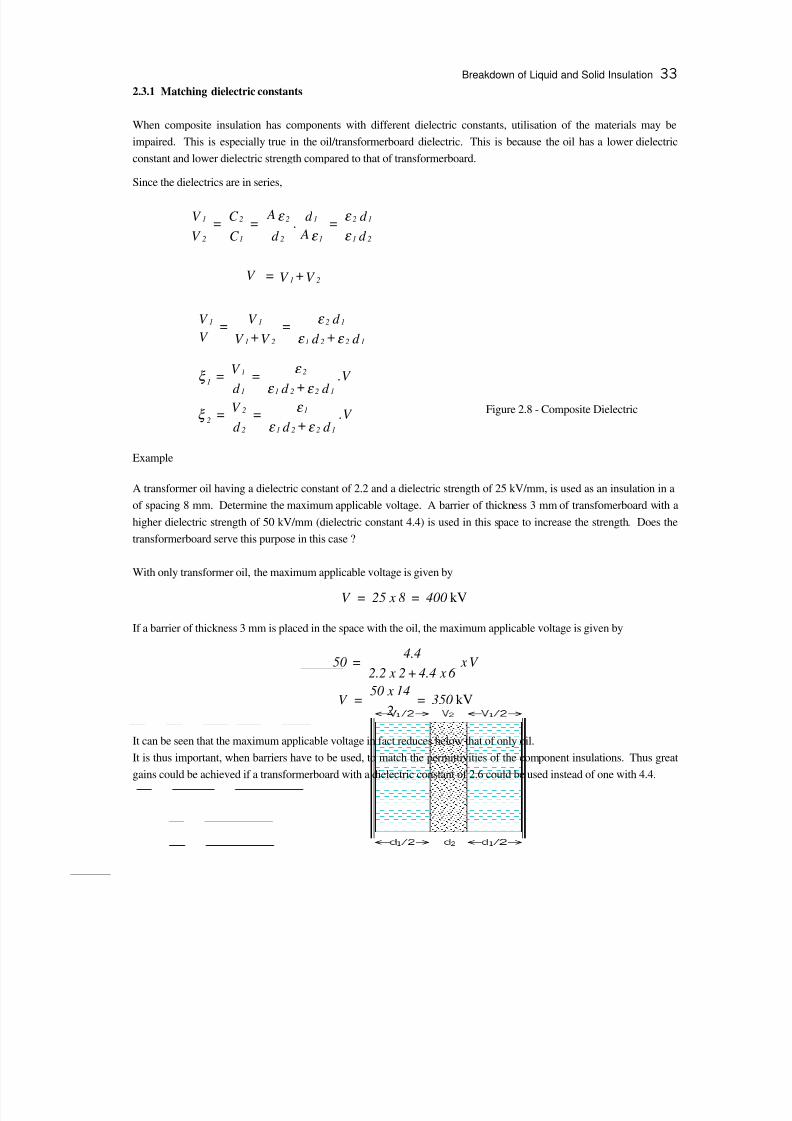
8/6/2019 High Voltage Engineering (Lucas)
http://slidepdf.com/reader/full/high-voltage-engineering-lucas 41/212
Breakdown of Liquid and Solid Insulation
2.3.1 Matching dielectric constants
When composite insulation has components with different dielectric constants, utilisation of the materials may beimpaired. This is especially true in the oil/transformerboard dielectric. This is because the oil has a lower dielectricconstant and lower dielectric strength compared to that of transformerboard.
Since the dielectrics are in series,
Example
A transformer oil having a dielectric constant of 2.2 and a dielectric strength of 25 kV/mm, is used as an insulation in aof spacing 8 mm. Determine the maximum applicable voltage. A barrier of thickness 3 mm of transfomerboard with a
higher dielectric strength of 50 kV/mm (dielectric constant 4.4) is used in this space to increase the strength. Does thetransformerboard serve this purpose in this case ?
With only transformer oil, the maximum applicable voltage is given by
If a barrier of thickness 3 mm is placed in the space with the oil, the maximum applicable voltage is given by
It can be seen that the maximum applicable voltage in fact reduces below that of only oil.It is thus important, when barriers have to be used, to match the permittivities of the component insulations. Thus greatgains could be achieved if a transformerboard with a dielectric constant of 2.6 could be used instead of one with 4.4.
Figure 2.8 - Composite Dielectric
V .d +d
= d V =
1221
2
1
11
ε ε ε ξ
V .d +d
= d V =
1221
1
2
22
ε ε ε ξ
d +
d
d =
V +
V
V = V V
V +V = V
d d =
Ad .
d
A =
C C =
V V
1221
12
21
11
21
21
12
1
1
2
2
1
2
2
1
ε ε
ε
ε ε
ε ε
kV400 = 8 x25 = V
kV350 = 2
14 x50 = V
V x6 x4.4+2 x2.2
4.4 = 50
'
'
/
/
/
'

8/6/2019 High Voltage Engineering (Lucas)
http://slidepdf.com/reader/full/high-voltage-engineering-lucas 42/212
Lightning Phenomena
3.1 Mechanism of Lightning
Lightning is an electric discharge in the form of a spark or flash originating in a charged cloud. It has now been known fora long time that thunder clouds are charged, and that the negative charge centre is located in the lower part of the cloudwhere the temperature is about - 5 0C, and that the main positive charge centre is located several kilometres higher up,where the temperature is usually below - 20 0C. In the majority of storm clouds, there is also a localised positively chargedregion near the base of the cloud where the temperature is 0 0C. Figure 3.1 shows such a cloud located above a overheadtransmission line.
Fields of about 1000 V/m exist near the centre of a single bipolar cloud in which charges of about 20 C are separated bydistances of about 3 km, and indicate the total potential difference between the main charge centres to be between 100 and1000 MV. The energy dissipated in a lightning flash is therefore of the order of 1000 to 10,000 MJ, much of which is spentin heating up a narrow air column surrounding the discharge, the temperature rising to about 15,000 0C in a few tens of microseconds. Vertical separation of the positive and negative charge centres is about 2 - 5 km, and the charges involved
are 10 - 30 C. The average current dissipated by lightning is of the order of kilo-amperes. During an average lightningstorm, a total of the order of kilo-coulombs of charge would be generated, between the 0 0C and the -40 0C levels, in avolume of about 50 km 3.
3.1.1 Breakdown Process
Under the influence of sufficiently strong fields, large water drops become elongated in the direction of the field andbecome unstable, and streamers develop at their ends with the onset of corona discharges. Drops of radius 2 mm developstreamers in fields exceeding a 9 kV/cm - much less than the 30 kV/cm required to initiate the breakdown of dry air. Thehigh field need only be very localised, because a streamer starting from one drop may propagate itself from drop to dropunder a much weaker field.
When the electric field in the vicinity of one of the negative charge centres builds up to the critical value (about 10 kV/cm),an ionised channel (or streamer) is formed, which propagates from the cloud to earth with a velocity that might be as highas one-tenth the speed of light. Usually this streamer is extinguished when only a short distance from the cloud.
+ +++++ + + + + ++ + +++++++ + + + + + + + + + cloud
+ + + + +++++ -20 0 C + + + + + + + + ++ + positive charge + + + + + + + + + + +
+ + - - - - + + + + + + ++ - - - - - - - negative charge + +
- - - - - - - - - - - - - - - - - -- - + ++ + - - - - - - - -5 0 C - - -
- - - + ++++ + 0 0 C - - - - - - - - - - -- - + ++ + - - - - - - - - - - -
+ + + + + + + +++ + + + + +FFFFFFFFFFFFFFFFFFFFFFFFFFFFFFFFFFFFFFFFFFFFFFFFFFFFFFFFFFFFFFFFFFFFFFFF7UDQVPLVVLRQ
Linetower
QQQQQQQQQHDUWK SODQH QQQQQQQQQQQQQQQQQQQQQQQQQQQQQQQQQQQQQQQQQQQQQQQQQQ
Figure 3.1 - Induced charges on transmission line

8/6/2019 High Voltage Engineering (Lucas)
http://slidepdf.com/reader/full/high-voltage-engineering-lucas 43/212
Lightning Phenomena 35
Forty micro-seconds or so after the first streamer, a second streamer occurs, closely following the path of the first, andpropagating the ionised channel a little further before i t is also spent. This process continues a number of times, each stepincreasing the channel length by 10 to 200 m. Because of the step like sequence in which this streamer travels to earth, thisprocess is termed the stepped leader stroke. This process is shown diagrammatically in figure 3.2.
When eventually the stepped leader has approached to within 15 to 50 m of the earth, the field intensity at earth is sufficientfor an upward streamer to develop and bridge the remaining gap. A large neutralising current flows along the ionised path,produced by the stepped leader, to neutralise the charge. This current flow is termed the return stroke and may carrycurrents as high as 200 kA, although the average current is about 20 kA.
The luminescence of the stepped leader decreases towards the cloud and in one instances it appears to vanish somedistance below the cloud. This would suggest that the current is confined to the stepped leader itself. Following the first,or main stroke and after about 40 ms, a second leader stroke propagates to earth in a continuous and rapid manner and againa return stroke follows. This second and subsequent leader strokes which travel along the already energised channel aretermed dart leaders .
What appears as a single flash of lightning usually consist of a number of successive strokes, following the same track inspace, at intervals of a few hundredths of a second. The average number of strokes in a multiple stroke is four, but as manyas 40 have been reported. The time interval between strokes ranges from 20 to 700 ms, but is most frequently 40-50 ms.The average duration of a complete flash being about 250 ms.
The approximate time durations of the various components of a lightning stroke are summarised as follows.
Stepped leader = 10 msReturn stroke = 40 V period between strokes = 40 msduration of dart leader = 1 ms
For the purpose of surge calculations, it is only the heavy current flow during the return stroke that is of importance. Duringthis period it has been found that the waveform can be represented by a double exponential of the form
i = I (e -. W- e - W)
with wavefront times of 0.5 - 10 V DQG ZDYHWDLO WLPHV RI- V $Q DYHUDJH OLJKWQLQJ FXUUHQW ZDYHIRUPhave a wavefront RI WKH RUGHU RIV DQG D ZDYHWDLO RI WKH RUGHU RIV
The standard voltage waveform used in high voltage testing has a 1.2/50 V ZDYHIRUP WR WDNH LQWR DFFRXQW WKH PRVWFRQGLWLRQV )RU WKH VWDQGDUG ZDYHIRUP WKH FRHIILFLHQWV. DQG LQ WKH GRXEOH H[SRQHQWLDO KDYH YDOXHV RI. [10 4 s-1, and [6 s-1.
+ + + + + + + + + + + ++ + + + + + + + + + + + + + + + + + + ++ + + + + + + +
- - - - - - - -- - - - - - - - - - - - - - - - - - - - - - - - - - - -
- - - - - - - - - - - - - - - - - - - -- - - -
- - - -- - - - - - - -
- - - -- - - - - -
- - - - - -- - - - - - - -
- - - - - -- -
- - - -- - + -
- + ++ +
++ +
+ ++ +
+ + + + + + + +++ + + + + +++++ + + + + +++++ + +FFFFFFFFFFFFFFFFFFFFFFFFFFFFFFFFFFFFFFFFFFFFFFFFFFFFFFFFFFFFFFFFFFFFFFFFFFFFFFFFFFF
Figure 3.2 - Propagation of lightning channel

8/6/2019 High Voltage Engineering (Lucas)
http://slidepdf.com/reader/full/high-voltage-engineering-lucas 44/212
High Voltage Engineering - J R Lucas 200136
3.1.2 Frequency of occurrence of lightning flashes
A knowledge of the frequency of occurrence of lightning strokes is of utmost importance in the design of protection againstlightning. The frequency of occurrence is defined as the flashes occurring per unit area per year.
However, this cannot be measured very easily, and without very sophisticated equipment. This information is difficult toobtain. However, the keraunic level at any location can be quite easily determined. The keraunic level is defined as thenumber of days in the year on which thunder is heard. It does not even distinguish between whether lightning was heardonly once during the day or whether there was a long thunderstorm. Fortunately, it has been found by experience that thekeraunic level is linearly related to the number of flashes per unit area per year. In fact it happens to be about twice thenumber of flashes/square mile/year. By assuming this relationship to hold good throughout the world, it is now possible toobtain the frequency of occurrence of lightning in any given region quite easily.
The isokeraunic level map, which shows contours of equal keraunic level, for Sri Lanka is shown in figure 3.3.
The map is based on the findings of the study “Lighning conditions in Ceylon,, and measures to reduce damage toelectricalequipment” by Dr Gi-ichi Ikeda in 1968 (Asian Productivity organization report, May 1969 – AP) Project TES/68)
3.2 Lightning Problem for Transmission Lines
The negative charges at the bottom of the cloud induces charges of opposite polarity on the transmission line. These are
held in place in the capacitances between the cloud and the line and the line and earth, until the cloud discharges due to alightning stroke. The figure 3.4 shows the problems facing the transmission engineer caused by lightning. There are threepossible discharge paths that can cause surges on the line.
Figure 3.3 - Isokeraunic Level map of Sri Lanka
55
63
74
98 35
24
36
11489
23
Estimated
below 30
30 to 50
60 to 80
90 to100 over
100below
40
around50
~ 80

8/6/2019 High Voltage Engineering (Lucas)
http://slidepdf.com/reader/full/high-voltage-engineering-lucas 45/212
Lightning Phenomena 37
(a) In the first discharge path (1), which is from the leader core of the lightning stroke to the earth, the capacitancebetween the leader and earth is discharged promptly, and the capacitances from the leader head to the earth wire and thephase conductor are discharged ultimately by travelling wave action, so that a voltage is developed across the insulatorstring. This is known as the induced voltage due to a lightning stroke to nearby ground . It is not a significant factor inthe lightning performance of systems above about 66 kV, but causes considerable trouble on lower voltage systems.
(b) The second discharge path (2) is between the lightning head and the earth conductor. It discharges the capaci tancebetween these two. The resulting travelling wave comes down the tower and, acting through its effective impedance, raisesthe potential of the tower top to a point where the difference in voltage across the insulation is sufficient to cause flashoverfrom the tower back to the conductor. This is the so-called back-flashover mode.
(c) The third mode of discharge (3) is between the leader core and the phase conductor. This discharges thecapacitance between these two and injects the main discharge current into the phase conductor, so developing a surge-
impedance voltage across the insulator string. At relatively low current, the insulation strength is exceeded and thedischarge path is completed to earth via the tower. This is the shielding failure or direct stroke to the phase conductor.
The protection of structures and equipment from the last mode of discharge by the application of lightning conductorsand/or earth wires is one of the oldest aspects of lightning investigations, and continue to do so.
3.2.1 Shielding by overhead ground wires
Overhead ground wires are provided on transmission lines to intercept direct strokes of lightning and thus keep it off thephase conductor, and to reduce the surge current and hence the overvoltage on a phase conductor by having currents
induced in it.
The proportion of lightning flashes capable of causing sparkover of line insulation decreases as the system voltageincreases. This is due to the fact that the magnitude of the overvoltage caused by lightning strokes are almost independentof the system voltage. Of course there is a slight dependence as the height of the towers also increase with the increase involtage and a taller tower is more liable to a lightning strike. For a given magnitude of lightning overvoltage, the per unitvalue based on system voltage decreases as the system voltage increases. Thus as the system voltage increases, there arelesser number of flashovers caused by lightning.
Not only does the tall tower attract more lightning strokes, but also it requires a much better earth-wire coverage for agiven degree of protection. The figure 3.5 il lustrates this geometrically, by consider ing two identical configurations of conductors, but with the height of the tower different.
- -- -
- - leader core2 - -
earth wire - - space charge envelope3 - -
tower → conductor
tower footing 1resistance
QQQQQQQQQQQQQQQQQQQQQHDUWK SODQH QQQQQQQQQQQQQQQQQQQQQQQQQQQQQQQ
Figure 3.4 - Geometry of lightning leader stroke and transmission line

8/6/2019 High Voltage Engineering (Lucas)
http://slidepdf.com/reader/full/high-voltage-engineering-lucas 46/212
High Voltage Engineering - J R Lucas 200138
The region marked (1) on the diagram, represents the region in which lightning will most likely strike the earth wire andthus provide protection against direct strikes. The locus of the lower boundary of this region is approximately defined bythe perpendicular bisector of the line joining the phase conductor (the outermost for a horizontal arrangement and theuppermost in the case of a vertical arrangement) and the earth wire.
The region marked (2) on the diagram, represents the region in which lightning avoids both the overhead conductor as wellas the earth wire but strikes some nearby object. The region has the upper boundary defined approximately by a paraboliclocus. This locus is taken as equidistant from both the earth plane as well as the phase conductor. This assumption is notexactly true as the phase conductor is a better attractor of lightning due to its sharper configuration).
Depending on the strength of the charge on the leader core, lightning will be initiated at a distance away from the objectstruck. Thus if the leader core could approach very close to the phase conductor before it discharges, then that particularstroke will be weak. This defines a minimum region within which lightning strikes terminating on the line does not do anydamage. This region thus has a circular locus around the conductor, which need not be considered.
The region marked (3) on the diagram is the balance region, demarcated by the locus of region (1), the locus of region (2)and the circular locus where the stroke is too weak to cause damage. In this region (3) the lightning stroke is most likely toterminate on the phase conductor. The area (3) is thus a measure of the efficiency of the earth-wire protection. The smallerthis region is the better the shielding provided by the overhead earth wires. It can be seen that for the same semi-verticalshielding angle WKH WDOOHU WKH WRZHU WKH OHVVHU WKH HIILFLHQF\ RI SURWHFWLRQ SURYLGHG E\ W
seen that if the semi-vertical angle of shielding is reduced, the area (3) reduces giving better protection. Thus to obtain thesame degree of protection, taller towers require smaller protection angles.
3.2.2 Calculation of Shielding angle
The shielding angle of an overhead earth wire is defined as the semi-vertical angle between the line joining the mostexposed conductor and the earth wire.
Consider the electrostatic interaction between the core of the downward lightning stroke and a single conductor and asingle earth wire as shown in figure 3.6. As the leader channel propagates downwards, its equipotential lines wil l interact
with both phase conductor as well as the earth wire. The earth wire may be at a lower potential than the phase conductoror vice versa. In the former case (a) protection will be afforded, and the shielding is effective. In the latter case (b) noprotection will be afforded and non-effective shielding will occur.
(1)
(1) (3) e
o oe (3) _
o o o o | o c_
o o | o c(2)
(2)
FFFFFFFFFFFFFFFFFFFFFFFFFFFFFFFFFFFFFFFFFFFFFFFFFFFFFFFFFFFFFFFFFFFFFFFFFFFFFFFFF //////////////////////////////// earth plane ////////////////////////////////////
Figure 3.5 - Earth wire shielding - geometric model
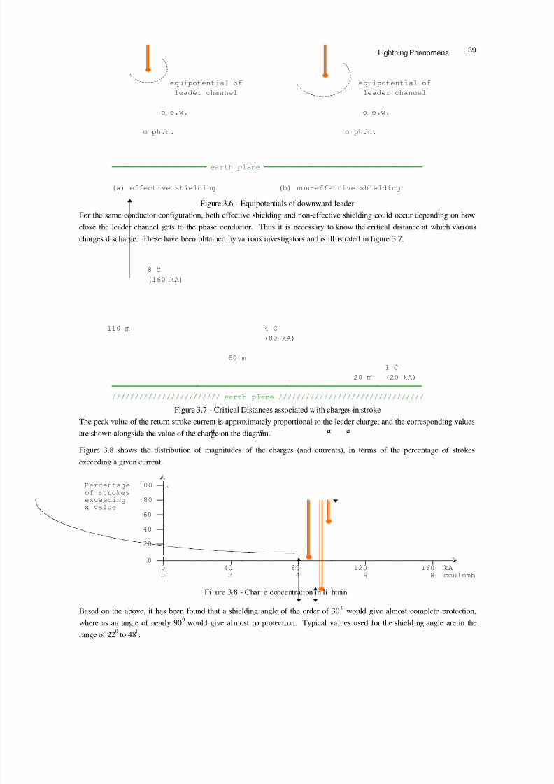
8/6/2019 High Voltage Engineering (Lucas)
http://slidepdf.com/reader/full/high-voltage-engineering-lucas 47/212
Lightning Phenomena 39
For the same conductor configuration, both effective shielding and non-effective shielding could occur depending on howclose the leader channel gets to the phase conductor. Thus it is necessary to know the critical distance at which various
charges discharge. These have been obtained by various investigators and is illustrated in figure 3.7.
The peak value of the return stroke current is approximately proportional to the leader charge, and the corresponding valuesare shown alongside the value of the charge on the diagram.
Figure 3.8 shows the distribution of magnitudes of the charges (and currents), in terms of the percentage of strokesexceeding a given current.
Based on the above, it has been found that a shielding angle of the order of 30 0 would give almost complete protection,where as an angle of nearly 90 0 would give almost no protection. Typical values used for the shielding angle are in therange of 22 0 to 48 0.
equipotential of equipotential ofleader channel leader channel
o e.w. o e.w.
o ph.c. o ph.c.
QQQQQQQQQQQQQQQQQQQQQHDUWK SODQH QQQQQQQQQQQQQQQQQQQQQQQQQQQQQQQQQQQ
(a) effective shielding (b) non-effective shielding
Figure 3.6 - Equipotentials of downward leader
8 C(160 kA)
110 m 4 C(80 kA)
60 m1 C
20 m (20 kA)QQQQQQQQQQQQQQQQQQQQQQQQQQQQQQQQQQQQQQQQQQQQQQQQQQQQQQQQQQQQQQQQQQQQ //////////////////////// earth plane ////////////////////////////////
Figure 3.7 - Critical Distances associated with charges in stroke
¿ Percentage 100 FM of strokes G exceeding 80 FM x value G
60 FM G
40 FM G
20 FM G
0 FPFFFFFFFFFFFFFFNFFFFFFFFFFFFFFNFFFFFFFFFFFFFFNFFFFFFFFFFFFFFNFFFF¾ 0 40 80 120 160 kA0 2 4 6 8 coulomb
Fi ure 3.8 - Char e concentration in li htnin

8/6/2019 High Voltage Engineering (Lucas)
http://slidepdf.com/reader/full/high-voltage-engineering-lucas 48/212
High Voltage Engineering - J R Lucas 200140
3.3 Area of attraction of transmission systems to lightning
Protective zone of lightning conductor : The area over which a lightning stroke will be attracted to and will terminate ona lightning conductor in preference to earth is termed the protection range or protective zone . Figure 3.9 shows thiszone.
The calculation of the area is based on a gradient of 3 kV/cm at the tower at which the upward streamer is initiated from thetower. It has been found that for the average stroke the protective ratio is approximately two for a lightning conductor ortower.
R = 2 H (approx) at 20 kA
That is, the area of attraction of a lightning conductor may be expected to be equal to an area around the base of theconductor with a radius of twice the conductor height. In the case of transmission lines, the earth wire is positioned toprotect the phase conductors against lightning strokes and hence it is a protective conductor. However, the earth wireattracts strokes that would not normally terminate on the line. Similar ly, phase-conductors themselves attract lightning
strokes and it is hardly correct to talk of the protective zone . A more appropriate term is the area of attraction . Figure3.10 shows the area of attraction of the transmission line and towers.
Since the tower is like a lightning conductor, the area of attraction of the tower can be taken as equal to a circle with radiustwice the tower height. An earth wire is more uniform that a transmission tower, in that it does not have a sharp point but asharp line. It has been estimated that an area either side of the earth wire to a distance of 1.5 or 1.6 times the effectiveheight of the ear th wire multiplied by the length of the earth wire is a reasonable value to be taken. Further it must be notedthat due to the sag of the earth wire, the effective height of the earth wire is itself only about 80% of the height at the tower.Thus a distance of 64% of the radius of attraction at the tower may be taken for the attraction distance of the earth wire.
The phase conductor may be treated similarly, but with the height of the phase conductor being considered instead of that of the earth wire.
Thus if the line dimensions are known, it is possible to evaluate the total area of attraction that the line has to lightningstrokes.
lightningconductor protective
zone
A = 2 5 2
Figure 3.9 - protective zone of lightning conductor
area of attraction
phase conductor rt rl = 0.64 rtFFFFFFFFFFFFFFFFFFFFFFFFFFFFFFFFFFFFFFFFFFFFFFFFFFFFFFFFFFFFFFFFFFFFFFFFFFFFFFFFFFFFFFFF
HFFI HDUWK ZLUH HFFI WRZHU HF FM LFFFFFFFFFFFFFFFFFFFFFFFFFFFFFFFFFFFFFFFM LFFFFFFFFFFFFFFFFFFFFFFFFFFFFFFFFFFFFFFM
JFFK SKDVH FRQGXFWRU JFFK JF FFFFFFFFFFFFFFFFFFFFFFFFFFFFFFFFFFFFFFFFFFFFFFFFFFFFFFFFFFFFFFFFFFFFFFFFFFFFFFFFFFFFFFFF
Figure 3.10 - Area of attraction of transmission line

8/6/2019 High Voltage Engineering (Lucas)
http://slidepdf.com/reader/full/high-voltage-engineering-lucas 49/212
Lightning Phenomena 41
3.4 Effects of Lightning on a Transmission Line
Charged clouds induce charges on upstanding objects. These induced charges are distributed in such a way as to cause aconcentration of potential at the upper end of the object, with the result that the electrostatic stress is very great. This
causes the air in the immediate neighborhood to be ionised very rapidly, and charged particles are expelled from thepointed end. This produces a gradual lowering of the resistance of the discharge path between the cloud and the conductoruntil eventually the lightning discharge takes place.
3.4.1 Strokes to a Phase-conductor
The charged cloud could discharge directly onto the line. If the line is struck a long distance from a station or substation,the surge will flow along the line in both directions, shattering insulators and sometimes even wrecking poles until all theenergy of the surge is spent. If it strikes the line immediately adjacent to a station, then the damage to plant is almostcertain, since it is doubtful whether the ordinary lightning arrestor could divert to earth such a powerful discharge, withoutallowing a part to be transmitted to the terminal apparatus.
When lightning strikes an overhead phase-conductor, the magnitude of the current and the high frequency nature of the strokecauses voltage surges to be propagated in both directions from the point of the strike (Figure 3.11).
The waveshape of these voltage surges is similar to that of the current in the lightning discharge. The discharge currentsplits itself equally on contact with the phase conductor, giving travelling waves of magnitude e.
e = ½ Z i ( e -. W- e - W)where Z is the surge impedance of the phase conductor.
Using a typical value for the line surge impedance (say 300 DQG DQaverage lightning current (20 kA), the voltage
waves on the line would have a crest value of
E = ½ Z i = (300/2) x 20 x 10 3 = 3 MV
3.4.2 Strokes to a tower with no earth wire
Fortunately, direct strokes to the line are infrequent in occurrence compared to side strokes, the effects of which are not sosevere. If there is a direct stroke to the tower, a current would be discharged through the metal work of the tower and therewould be a potential difference between the top and bottom of the tower.
Figure 3.12 shows a steel tower (inductance L) of a transmission line with no earth wire. If the earthing resistance of thetower is R (= 5 - 100 DQG LW LV VWUXFN E\ OLJKWQLQJ WKHQ WKH SRWHQWLDO EXLOW XS RQ WKe tower top would be
i
phase conductor ½ i ½ i
FFFFFFFFFFFFFFFFFFFFFFFFFFFFFFFFFFFFFFFFFFFFFFFFFFFFFFFFFFFFFFFFFFFFFFFFFFFF e = ½ Z i e = ½ Z i
Tower Tower
*********************************** earth ***********************************
Figure 3.11 - Direct strike on phase conductor
t d id
L+i R

8/6/2019 High Voltage Engineering (Lucas)
http://slidepdf.com/reader/full/high-voltage-engineering-lucas 50/212
High Voltage Engineering - J R Lucas 200142
e+t d id
L+i R = e i
If e i is the induced voltage on the conductor due to the lightning, then thepotential difference built up across the tower and the conductor is given by
If the value of e exceeds the line insulation strength, then a flashover occursfrom the tower to the line and this is termed a backflashover .
3.4.3 Strokes to Earth Wire
When a lightning stroke terminates on the tower of a transmission line havingan overrunning earth wire, or terminates on the earth wire of the transmissionline, then the resulting current flow would be as shown in figure 3.13 (a) and(b).
The voltage waves produced by the current i w flowing along the earth wire will travel along the earth wire in bothdirections from the tower struck. On reaching the neighboring towers they wil l be partly reflected, and the reflected waveswill arrive back at the tower after twice the transit time between the towers. Further reflections will take place as thewaves travel further along the earth wire and reaches other towers. In calculation of the resulting voltage wave and hencethe potential difference across the insulation it is useful to consider the initial period , first reflection period , secondreflection period and so on and obtain separate equivalents.
For example, for the initial period and the first reflection period, the following equivalent circuits given in figures 3.14 and3.15 may be used.
Initial period
R aQQQV R R R R R R R EDFN
Tower R IODVKRYHU R R R R G HOI
R G G G G JNK FOF F
Figure 3.12 - Strokes to tower
i i
earth wire i w i w i w i w
FFFFFFFFFFFFFFFFFFFFFFFFFFFFFFFFFFFFFFFFFFF FFFFFFFFFFFFFFFFFFFFFFF
iTower t Tower
**************** earth *********************** **************************
(a) Stroke to tower (b) Stroke to mid-span
Figure 3.13 - Stroke to earth wire
earth wire
TowerLR
******* earth ********************** ************************(a) Part of system (b) Equivalent circuit
Figure 3.14 - For initial period
q
iwiw
Z Z
it
q
2 iw
Z/2
it
C
ec
L
R

8/6/2019 High Voltage Engineering (Lucas)
http://slidepdf.com/reader/full/high-voltage-engineering-lucas 51/212
Lightning Phenomena 43
In the figure 3.14, L is the effective inductance of the tower, R is the effective resistance of the tower and footing and Z isthe surge impedance of the earth wire.
First Reflection period
If instead of the actual tower being struck, the earth wire is struck somewhere near mid-span, then this can be regarded astwo towers in parallel being struck for the second reflection period, with the impedance of the span struck acting as anextension to the lightning channel.
For a given tower footing resistance R, strokes to the tower generally develop about one-and-half times the potential at thetop of the tower as compared with the strokes to mid span. For a typical lightning current of 20 kA and a tower footing
resistance of 20 WKRVH VWUXFN DW WKH WRZHU GHYHORS YROWDJHV RI WKH RUGHU RI N9
3.4.4 Strokes to nearby objects (Indirect Strokes)
In any lightning discharge, the charge on the down coming leader causes the conductors of the line to have a charge inducedin them (figure 3.16).
These charges are bound (held in that portion of the line nearest to the cloud) so long as the cloud remains near withoutdischarging its electricity by a lightning stroke to an object. If however, the cloud is suddenly discharged, as it is whenlightning strikes some object nearby, the induced charges are no longer bound, but travel with nearly the velocity of light,along the line to equalise the potential at all points of the line.
Earth wire
TowerLR
********** earth **************************** *******************************
(a) Part of system (b) Equivalent circuit
Figure 3.15 - For first reflection period
where L' is the inductance of the first span loop and earth return.
+ + + + ++ + + + + +
+ + + + + Cloud - - - -- - - - - -
- - - - -- - - - -
- -
C1
+ + + + + + + + ++++++ + + + + + + + +
Tower C2
***************************** earth *****************************************
Figure 3.16 Induced charge on line
q
iwiw
Z Z
it
q
L′ / 2
R′ /2 it
C
ec
L
RR′
L′ L′
Z/2

8/6/2019 High Voltage Engineering (Lucas)
http://slidepdf.com/reader/full/high-voltage-engineering-lucas 52/212
High Voltage Engineering - J R Lucas 200144
C q
=C +C
C . E -=e21
2i
q
q/2 q/2 e ie i
This bound charge collapse leads to a voltage wave to be generated on the line in either direction.The value of this is given by
where q = bound charge per unit length of line
C = capacitance per unit length of line
This potential will vary along the line depending upon the distance of each element of line from the lightning stroke.
The sequence of the travelling waves e i propagating outwards is shown diagrammatically in figure 3.17
+ + ++ + + +
Cloud + + + + + +- - - - - - -
- - - - -- - - - - -
stroke to nearby earth
bound charge due tocharge release due down coming leader (t=0)
to return stroke(t1 > 0)
travelling waves(t 2 > t 1 )
FFFFFFFFFFFFFFFFFFFFFFFFFFFFFFFFFFFFFFFFFFFFFFFFFFFFFFFFFFFFFFFFFFFF
Figure 3.17 - Propagation of travelling waves

8/6/2019 High Voltage Engineering (Lucas)
http://slidepdf.com/reader/full/high-voltage-engineering-lucas 53/212
High Voltage Transient Analysis
4.1 Surges on Transmission Lines
Due to a variety of reasons, such as a direct stroke of lightning on the line, or by indirect strokes, or byswitching operations or by faults, high voltage surges are induced on the transmission line. The surge can beshown to travel along the overhead line at approximately the speed of light. These waves, as they reach theend of the line or a junction of transmission lines, are partly reflected and partly transmitted. These can be
analysed in the following manner.
Consider a small section of the transmission line, of length dx .
Let the voltage variation across this section at any instant of time be e to dx. xe
+e∂∂
, and let the current
vary similarly.
Due to the surge, the voltage build-up in the line travels along the line and would cause damage to thetransformer and other terminal equipment.
Let e = instantaneous voltage (varies with both distance and time)i = instantaneous current (varies with both distance and time)r = resistance of line per unit lengthl = inductance of line per unit lengthc = capacitance of line per unit lengthg = conductance of line per unit length
The voltage drop across PQ and the corresponding current through it are given by
the following equations.
P i Q dx. xi
+i∂∂
FFFFFFFFFFFFFFFFFFFFFFFFF>FFFFFFFFF>FFFFFFFFFFFFFFFFFFFFFFFFFF
sending end e dx. xe
+e∂∂
receiving end
FFFFFFFFFFFFFFFFFFFFFFFFFFFFFFFFFFFFFFFFFFFFFFFFFFFFFFFFFFFFFF
½ FFFFFFFFF x FFFFFFFFF¾½ FF dx FF¾
Fi ure 4.1 - Element of transmission line

8/6/2019 High Voltage Engineering (Lucas)
http://slidepdf.com/reader/full/high-voltage-engineering-lucas 54/212
High Voltage Engineering - J R Lucas, 2001
Eliminating dx gives us the partial differential equations
Differentiating equation (1) with respect to x, and equation (2) with respect to t, and eliminating i, we have
A very similar partial differential equation can be obtained for i.
In practical power lines, the resistance r is much less than the inductance l, and the conductance g is negligible.When these are neglected, the equation reduces to
It is usual to substitute l.c = 1/a2, where a has the dimension of velocity. In this case the equation becomes
The solution to this second order partial differential equation can be written in the form of two arbitraryfunctions.
Consider the function e = f(x - at) . For this
)a(-.t)a-(xf"=t
e also 2
2
2
∂∂
∂∂ ,t)a-(x f"a=
x
e a 2
2
22
It is thus seen that this function satisfies the partial differential equation.
Similarly, consider the function e = F(x + at) . For this
)(a.t)a+(xF"=t
e also 2
2
2
∂∂
∂∂ ,t)a+(xF"a=
x
e a 2
2
22
This too is seen to satisfy the partial differential equation.
Thus the general solution to the partial differential equation is
e = f(x - at) + F(x + at)
where f and F are two arbitrary functions of (x-at) and (x+at) . These two functions can be shown to beforward and reverse traveling, as follows.
t
e dxc+edxg=dx.
x
i -=i
t i
dxl+idxr =dx. xe
-=v
∂
∂
∂
∂∂∂
∂∂
(2) t e
c+eg= xi
-
(1) t i
l+ir = xe
-
∂∂
∂∂
∂∂
∂∂
er .g+t
e .g)l+.r (c+
t
e c.l=
x
e 2
2
2
2
∂
∂
∂
∂
∂
∂
t
e c.l=
x
e 2
2
2
2
∂∂
∂∂
t e =
xe a 2
2
2
22
∂∂∂∂

8/6/2019 High Voltage Engineering (Lucas)
http://slidepdf.com/reader/full/high-voltage-engineering-lucas 55/212
High Voltage Transient Analysis Consider a point x1 at an instant t1 on a transmission line.
The value of the function f(x-at) at position x1 and time t1 would be
e1 = f(x 1 - a t 1)
At any time t afterwards (i.e. at time t+t 1), the value of this same function at the position x would be given by
e2 = f[x - a (t+t 1)] = f(x-at + a t 1)
This latter voltage e2 would be equal to e1 at the position x1 = x - at .
Now a.t is the distance traveled by a wave traveling with velocity a in the forward direction in a time t .Thus it is seen that the voltage at a distance a.t in the forward direction is always equal to the value at theearlier position at the earlier time for any value of time. Thus the function f(x-at) represents a forward wave .Similarly, it can be seen that the function F(x+at) represents a reverse wave.
The effect of resistance and conductance, which have been neglected would be so as to modify the shape of the wave, and also to cause attenuation. These are generally quite small, and the wave travels with littlemodification. In fact this effect can be separately included in the analysis as will be shown later.
4.1.1 Surge Impedance and Velocity of Propagation
Consider the forward wave e = f(x-at) . The corresponding current wave i can be determined from equation(1) as follows.
Zo is known as the surge (or characteristic) impedance of the transmission line.
The surge current i traveling along the line is always accompanied by a surge voltage e = Z o i travelingin the same direction. For a reverse wave, it can be similarly shown that the surge current i is associated witha surge voltage e = - Z o i.
For a transmission line, with conductors of radius r and conductor spacing d , it can be shown that the
inductance per unit length of the line is given by
½ FFFFFFFFF x 1 FFFFFFFFFFF¾ t 1
sending end FFFFFFFFFFFFFFFFFFFFFFFFFFx FFFFFFFFFFFFFFFFFFFFFFFFFF receiving end
Figure 4.2 - Position (x 1, t1) on transmission line
cl
=Z where i.Z=i.cl
=e .e.i 00
e.lc
=e.la
1 =at)-(x f
la1
=i
t)a-(x f -= xe
-=t e
l
∴
′∂∂
∂∂
H/mlog r d
+4
2
= l er 0 µ
π µ

8/6/2019 High Voltage Engineering (Lucas)
http://slidepdf.com/reader/full/high-voltage-engineering-lucas 56/212
High Voltage Engineering - J R Lucas, 2001
Since the internal flux linkage is small, if this is neglected
The capacitance c per unit length is given by
Therefore the velocity of propagation of the wave a is equal to the velocity of light. [Note: If the resistance of the line was not neglected, the velocity of propagation of the wave would be found to be slightly less than thatof light (about 5 to 10%)].
For a cable, the dielectric material has a relative permittivity 0 r different from unity. In this case, the abovederivation would give the velocity of propagation in a cable as
velocity of propagation = velocity of light/ √0r
For commercial cables, 0r lies between about 2.5 and 4.0, so that the velocity of propagation in a cable isabout half to two-third that of light.
The surge impedance of a line can be calculated as follows.
Substituting the velocity of light as 3 x 10⁸
m/s and simplifying gives
Zo = 60 log e (d/r)
For an overhead line, for practical values of conductor radius r and spacing d , the surge impedance Zo is of theorder of 300 to 600
For a cable, the corresponding surge impedance would be given by the expression
Zo = 60/ √0r . log e (d/r)
which has values in the region of 50 to 60
H/mlog r d
2
= l e0
π µ
lightof velocity= 1
but
a
1 ==c.l
1= airfor
F/mlog
00
200
r
ε µ
ε µ
ε
ε ε π
∴
r d
2 =c
e
r 0
2
/r d =
cl
= Z e
2
0
00
log
ε
µ
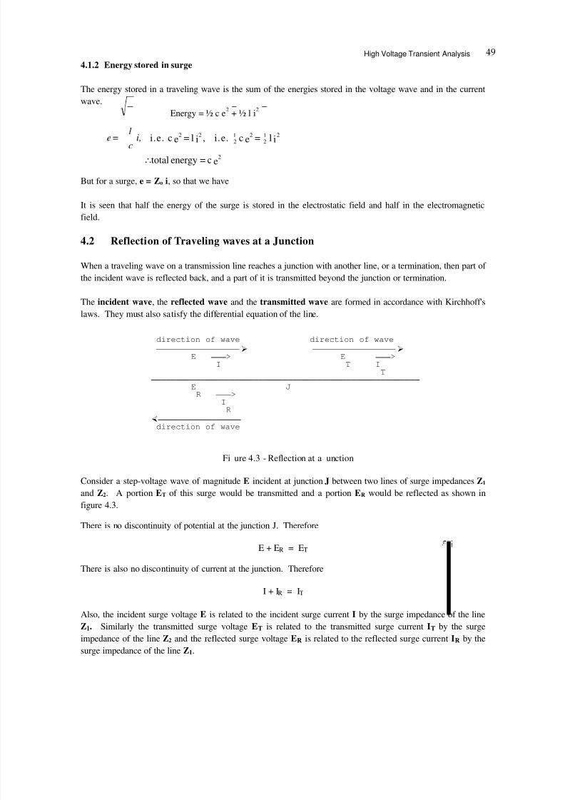
8/6/2019 High Voltage Engineering (Lucas)
http://slidepdf.com/reader/full/high-voltage-engineering-lucas 57/212

8/6/2019 High Voltage Engineering (Lucas)
http://slidepdf.com/reader/full/high-voltage-engineering-lucas 58/212
High Voltage Engineering - J R Lucas, 2001
However it is to be noted that the reflected wave is a reverse wave. Thus we can write
E = Z 1 I , E T = Z2 IT , and E R = - Z 1 IR Substituting these values gives
E/Z1 - E R /Z1 = E T /Z2 = (E + E R)/Z2
This gives on simplification
Similarly, the transmitted surge may be written as
Thus we have obtained the transmitted wave E T and the reflected wave E R in terms of the incident surge E.Since both these surges are a definite fraction of the incident surge, a transmission factor . and a reflectionfactor are defined as follows.
When the junction is matched (i.e. Z 1 = Z 2), then there is no reflection and the reflection factor can be seen tobe zero.
When the line Z 1 is open circuited at the far end (i.e.
Z2 = ∞), then the full wave is reflected back and thereflection factor becomes 1.
When the line Z 1 is short circuited at the far end (i.e.Z2 = 0), then no voltage can appear and the full waveis reflected back negated so as to cancel the incidentwave and the reflection factor becomes - 1.
4.2.1 Open circuited line fed from a infinite source
For this case Z 2 =∞
and
When a voltage surge E arrives at the junction J,which is on open circuit, it is reflected without achange in sign (i.e. E ).
Also, a current surge ( - I ) of opposite sign to theincident ( I ) is reflected so that the transmitted currentis zero.
If the line is fed from a constant voltage source E ,
then as the reflected voltage surge ( E) arrives at thegenerator end, since the generator maintains thevoltage at its end at voltage E , it send a voltage surgeof -E back to the line so as to keep its voltage at E .
E . Z + Z Z - Z = E
12
12 R
E . Z + Z
Z 2 = E
12
2T
Z + Z Z - Z = ,
Z + Z Z 2
= 12
12
12
2 β α
open circuited line
JE FFFFFFFFFFFFFFI G
FFFFFFFFFFFFFFOFFFFPFFFFFFFFF0I FFFFFFFFFFFFFFI G
FFFFFFFFFFFFFFOFFFFPFFFFFFFFF0incident step waves
G 2E HFFFFFFPFFFFFFFI 2E
E FFFFFFFFFFFFOFFFFFFM G FFFFFFFFFFFFFFFFFFFPFFFFFFFOF0
I FFFFFFFFFFFFFFFFFFFM FFFFFFFFFFFFNFFFFFFPFFFFFFFFF0
-I JFFFFFFM just after reflection at J
2E FFFFFFFFFFFFFFFFFFFPFFFFFFFF2EG
FFFNFFFFFFFFFFFFFFFPFFFFFFFF 0FFFK -E G
FFFNFFFFFFFFFFFFFFFPFFFFFFFF 0FFFK -I G
after reflection at gen. end
G HFF 2EE FFFFFFFFFFFFFFFFFFFM G
FFFFFFFFFFFFFFNFFFFPFFFFFOFFF0-E JFFFFM
I HFFFFM FFFFFFFFFFFFFFOFFFFPFFFFFFFFF0-I FFFFFFFFFFFFFFFFFFFM
after 2nd reflection at J
Fi ure 4.4 - Reflections under o en circuit conditions

8/6/2019 High Voltage Engineering (Lucas)
http://slidepdf.com/reader/full/high-voltage-engineering-lucas 59/212

8/6/2019 High Voltage Engineering (Lucas)
http://slidepdf.com/reader/full/high-voltage-engineering-lucas 60/212
High Voltage Engineering - J R Lucas, 2001
If we consider the peak value of the sinusoidal voltage as 1 pu , then if we deviate from this position by 1.8 o,then the corresponding voltage would be cos 91.8 o = 0.9995 pu . During this interval, it can be seen that thevariation of the voltage is negligibly small and the step approximation can be considered valid. Even in otherinstances, the step analysis is useful because other waveforms can be considered as made up of step surges.
4.3 Bewley Lattice Diagram
This is a convenient diagram devised by Bewley, which shows at a glance the position and direction of motionof every incident, reflected, and transmitted wave on the system at every instant of time. The diagramovercomes the difficulty of otherwise keeping track of the multiplicity of successive reflections at the various
junctions.
Consider a transmission line having a resistance r , an inductance l, a conductance g and a capacitance c, allper unit length.
If is the propagation constant of the transmission line, andE is the magnitude of the voltage surge at the sending end,
then the magnitude and phase of the wave as it reaches any section distance x from the sending end is E x givenby.
wheree- . [ represents the attenuation in the length of line xe-j [ represents the phase angle change in the length of line x
Therefore,. attenuation constant of the line in neper/km
phase angle constant of the line in rad/km.
It is also common for an attenuation factor k to be defined corresponding to the length of a particular line. i.e.k = e - . Ofor a line of length l.
The propagation constant of a line RI D OLQH RI VHULHV LPSHGDQFHz and shunt admittance y per unit length isgiven by
Similarly the surge impedance of the line (or characteristic impedance) Zo
When a voltage surge of magnitude unity reaches a junction between two sections with surge impedances Z1 and Z2, then a part . is transmitted and a part is reflected back. In traversing the second line, if theattenuation factor is k , then on reaching the termination at the end of the second line its amplitude would bereduced to N. . The lattice diagram may now be constructed as follows. Set the ends of the lines at intervalsequal to the time of transit of each line. If a suitable time scale is chosen, then the diagonals on the diagramshow the passage of the waves.
ee E =e. E =e. E = E x j- x- x) j+(- x- x
β α β α γ
c) j+(gl) j+(r = z.y= ω ω γ
c) j+(gl) j+(r
= y z
= Z 0ω ω

8/6/2019 High Voltage Engineering (Lucas)
http://slidepdf.com/reader/full/high-voltage-engineering-lucas 61/212
High Voltage Transient Analysis
In the Bewley lattice diagram, the following properties exist.
(1) All waves travel downhill, because time always increases.
(2) The position of any wave at any time can be deduced directly from the diagram.
(3) The total potential at any point, at any instant of time is the superposition of all the waves which have
arrived at that point up until that instant of time, displaced in position from each other by intervalsequal to the difference in their time of arrival.
(4) The history of the wave is easily traced. It is possible to find where it came from and just what otherwaves went into its composition.
(5) Attenuation is included, so that the wave arriving at the far end of a line corresponds to the valueentering multiplied by the attenuation factor of the line.
4.3.1 Analysis of an open-circuit line fed from ideal source
Let 2 is the time taken for a wave to travel from one end of the line to the other end of the line (i.e. single
transit time) and k the corresponding attenuation factor.
Consider a step voltage wave of amplitude unity starting from the generator end at time t = 0. Along the linethe wave is attenuated and a wave of amplitude k reaches the open end at time 2 . At the open end, this waveis reflected without a loss of magnitude or a change of sign. The wave is again attenuated and at time 2 reaches the generator end with amplitude k 2. In order to keep the generator voltage unchanged, the surge isreflected with a change of sign ( -k 2), and after a time 32 reaches the open end being attenuated to -k 3. It is thenreflected without a change of sign and reaches the generator end with amplitude -k 4 and reflected withamplitude +k 4. The whole process is now repeated for the wave of amplitude k 4.
The corresponding lattice diagram is shown in figure 4.6. At the receiving end of the line, the transmittedsurge is twice the incident surge. [This can be obtained from either the transmission coefficient, or by addingthe incident and reflected surges which make up the transmitted surge]. At any given instant, the voltage atthis end is the summation of the surges arriving until that instant of time.
Thus the voltage at the open end after the n th reflection is given by
Vr = 2 (k - k 3 + k 5 - k 4 + .... k 2n-1 )
0 L F F F F F F F F F F F F F F F F F F F F F M 0
G +1 G G +k G
2 L F F F F F F F F F F F F F F F F F F F F F M 2 G +k G G +k 2 G
2 2 L F F F F F F F F F F F F F F F F F F F F F M2 2 G G -k 2 G G G -k 3 G G
3 2 L F F F F F F F F F F F F F F F F F F F F F M3 2 G
G -k 3 G 6 G -k 4 G time
4 2 L F F F F F F F F F F F F F F F F F F F F F M4 2 G +k 4 G G +k 5 G
5 2 L F F F F F F F F F F F F F F F F F F F F F M5
Fi ure 4.6 - Lattice dia ram for an o en-circuited line

8/6/2019 High Voltage Engineering (Lucas)
http://slidepdf.com/reader/full/high-voltage-engineering-lucas 62/212
High Voltage Engineering - J R Lucas, 2001
This is a geometric series which has the summation given by
It is thus seen that when attenuation is present, the receiving end voltage is less than the sending end voltage.The reason for this is that there is a voltage drop in the line due to the shunt capacitive currents flowing in theline even on open circuit. However, since k is very close to 1, the reduction is very very small. [For example,even for k = 0.90, the corresponding reduced value is 2x0.90/(1+0.90 2) = 0.9944].
Let us now consider a line terminated through a resistance R. The corresponding reflection coefficient at thereceiving end would be 5 -Z 1)/(R+Z 1) and the reflection factor at the sending end would still be -1. Thus in addition to the attenuation occurring on the line, there is a non complete reflection occurring at the farend of the line. This would have a lattice diagram as shown in figure 4.7.
The final voltage attained at the resistive termination will now depend on both the attenuation and the reflectioncoefficient. From the lattice diagram it can be seen that this value can be calculated as follows.
1<k +1k 2
.e.i
k 2>k +1 0,>)k -1(
k +1k 2
=V
n,tvaluefinalfor the
2
22
2r∴
∞→∞→
)k -(-1)k -(-1
k 2=V 2
n2
r
0 L F F F F F F F F F F F F F F F F F F F F F M 0
G +1 G G +k G
2 L F F F F F F F F F F F F F F F F F F F F F M 2
G + k G G + k 2 G 2 2 L F F F F F F F F F F F F F F F F F F F F F M2 2 G
G - k 2 G G G - k 3 G G
3 2 L F F F F F F F F F F F F F F F F F F F F F M3 2 G G - 2 k 3 G À G - 2 k 4 G time
4 2 L F F F F F F F F F F F F F F F F F F F F F M4 2 G + 2 k 4 G G + 2 k 5 G
5 2 L F F F F F F F F F F F F F F F F F F F F F M5 2
Fi ure 4.7 - Lattice dia ram for a resistive termination

8/6/2019 High Voltage Engineering (Lucas)
http://slidepdf.com/reader/full/high-voltage-engineering-lucas 63/212
High Voltage Transient Analysis
Therefore, again, the receiving end voltage is less than the sending end voltage. However if there is noattenuation (k = 1), then the receiving end voltage tends to unity as shown in figure 4.8.
4.2.3 Reflections at 3 substation system
Consider 3 substations (1), (2) and (3) connected by lines Z 1, Z2, Z3 and Z 4, as shown in figure 4.9. Let . DQG
.EH WKH WUDQVPLVVLRQ FRHIILFLHQWV IRU D ZDYH LQFLGHQW DW WKH VXEVWDWLRQ IURP W
KDQG VLGH UHVSHFWLYHO\ DQG OHWDQG EH WKH Forresponding reflection factors.
In the Bewley lattice diagram, the junctions must be laid off at intervals equal to the time of transit of eachsection between junctions. (If all lines are overhead lines, then the velocity of propagation may be assumed tobe the same and the junctions can be laid off proportional to the distance between them. Otherwise this is notpossible).
The lattice diagram is shown together with the system diagram, and a unity magnitude surge is assumed toarrive from outside the on line 1.
1<k +1
k )+(1 .e.i 2β
β
β β
β β
β β
β β β β β
0> k -k -k +1
,0>)k -1()k -1( 1,<k 1,<k
k +1k )+(1
=V
......-k +k +k -k -k +k =V
2
2r
5352323r
¿ Vr 2.0 M
G HFFFFFFFI G G G G G G HFFFFFFFI G G G G G G G G G G HFFFFFFFI G G G G G G G G G G G G G G HFF G G G G G G G G G G G G G G G G
1.0 P F P F F F P F F F P F F F P F F F P F F F P F F F P F F F G G G G G G G G G G G G G G G G G G G G G G G G G G G G G G JFFFFFFFK
G G G G G G G G G G JFFFFFFFK G G G G G G JFFFFFFFK G G JFFFPFFFNFFFNFFFNFFFNFFFNFFFNFFFNFFFNFFFNFFFNFFFNFFFNFFFNF¾
0 2 3 2 5 2 7 2 9 2 11 2 13 2 time
Figure 4.8 - Receiving end voltage with resistive termination

8/6/2019 High Voltage Engineering (Lucas)
http://slidepdf.com/reader/full/high-voltage-engineering-lucas 64/212
High Voltage Engineering - J R Lucas, 2001
Example:
3 substations A, B and C are spaced 75 km apart as shown in figure 4.10. B and C are connected together bya cable (velocity of propagation 2 x 10 8 m/s), and the remaining connections are all overhead lines (velocity of propagation 3 x 10 8 m/s). The attenuation factors and the surge impedances of the lines are shown alongsidethe lines. The overhead lines beyond A and C on either side are extremely long and reflections need not beconsidered from their far ends. Determine using the Bewley lattice diagram the overvoltages at the 3substations, at an instant 1_ ms after a voltage surge of magnitude unity and duration ¾ reaches the substationA from the outside.
The transmission and reflection coefficients can be calculated as follows.
At A,
similarly, at B
reflection coeff. 1<-> 1 2 <-> 2 3 <-> 3
transmission coeff. . 1<-> . 1
' . 2 <-> . 2
' . 3 <-> . 3
'
attenuation factor HFFI k2 HFFI k3 HFFI FFFFFM1 LFFFFFFFFFFFFFFFFFFFM2 LFFFFFFFFFFFFFM3 LFFFFFFFFF
surge impedance Z1 JFFK Z2 JFFK Z3 JFFK Z4
1HFFFFFFFFFFFFFFFFFFFFFFFNFFFFFFFFFFFFFFFI G. G G
1 G 1 G G G G G G k . G G G 2 1 G k . . G G M 2 1 2 G G G G G G G G G G k k . . . G G M 2 3 1 2 3G G G L G G G G G G M G G G G
G G G G G G G G G G L M G G G G G L G G G G G G
À G M M
G G G time L G G G G G G P M G G G L G G G G G G P M G G G L G G G G G G P M G G G L G G G G G G P M
Figure 4.9 - Bewley Lattice Diagram
0.8=10002x400
= 1.2=1000
600 x2 =
0.2-= 0.2=400+600400-600
=
11
11
α α
β β
′
′
1.8=666 2x600
= 0.2=666
66 x2 =
0.8= 0.8-=600+66 600-66
=
322
32
32
2
23232
2
α α
β β
′
′

8/6/2019 High Voltage Engineering (Lucas)
http://slidepdf.com/reader/full/high-voltage-engineering-lucas 65/212
High Voltage Transient Analysis
similarly, at C it can be shown that
3 = 0.8, 3' = - 0.8, . 3 = 1.8, and . 3' = 0.2.
The single transit times of the two lines connecting the substations are
2AB = 75 x 10 3 /3 x 10 8 = ¼ ms, 2BC = 75 x 10 3 /2 x 10 8 = _ ms .
The lattice diagram must be set out, such that the intervals AB and BC are in the proportions to the times 1/4ms and 3/8 ms respectively. These are shown in figure 4.10 .
Since the step voltage incident at substation A is of duration 3/4 ms, only reflections that have occurred after3/4 ms prior to the present will be in existence.
at time t = 1_ ms,
voltage at junction A = - 0.080 + 0.143 -0.010 = 0.053 puvoltage at junction B = 0.199 + 0.004 + 0.032 + 0 = 0.235 pu
Since a surge arrives at junction C at the instant of interest, we can define values either just before or just afterthe time.
voltage at junction C at t - = 0.040 + 0.127 = 0.167 puvoltage at junction C at t + = 0.040 + 0.127 + 0.005 = 0.172 pu
HFI N HFI N HFI FFFFFFFM$ LFFFFFFFFFFFFFFFFFFFFFM%LFFFFFFFFFFFFFFFFFFFFFFFFFFFFFFFFFFM&LFFFFFF
JFK JFK B JFK
1HFFFFFFFFFFFFFFFFFFFFFFFNFFFFFFFFFFFFFFFFFFFFFFFFFFFFFFFFFFFFI
0.2 G1.2 G G G G L G G G G M L G G G G -0.864 G L
G-0.778 G G -0.622 L 0.156 G L
G G G G G G P G G G 0.138 G G G M L À G G G
time G -0.112 G L G-0.100 G G
-0.080 L 0.020 M L G G G G G P G 179 0.018 G 0.018 G
0.143 L -0.036 M L G G G
G -0.014 G P G-0.013 -0.032 G 0.056 G -0.010 L 0.003 M L
G G G G G P G G 0.002 G
0 L 0 M L G G G
Fi ure 4.10 - Exam le of a lication of Bewle Lattice dia ram

8/6/2019 High Voltage Engineering (Lucas)
http://slidepdf.com/reader/full/high-voltage-engineering-lucas 66/212
High Voltage Engineering - J R Lucas, 2001
Reflection and Transmission at a T-junction
When the intersection occurs between more than two lines, the analysis can be done as follows. Consider theconnection shown in figure 4.11.
If a surge voltage of magnitude E is incident on the junction with two other lines (Z 2 and Z 3) from a line (Z 1),then the transmitted and reflected surges would be as shown. For these
E = Z 1 I, E r = - Z 1 Ir, E2 = Z2 I2 , and E 3 = Z3 I3
Also, considering the fact that the total voltage and the current on either side of the junction must be the same,
E2 = E 3 = E T = E r + E, and I r + I = I 2 + I3
These may be solved to give the following expressions for the transmitted and reflected surges.
The method can be extended to junctions with more than 3 lines. However, there is an easier method of analysis to obtain the same result.
For a surge, the voltage and the current are always related by the surge impedance, independent of thetermination of the line at the far end. Thus for analysis purposes, the line behaves similar to a load of impedance Z0 connected between the start of the line and the earth. Thus when a single line ( Z1) feeds twoother lines (Z 2 and Z 3), the resultant reflections and transmissions could be obtained by considering both theselines as impedances connected from the junction to earth. That is, these two lines behave for surge purposesas if their surges impedances were connected in parallel.
FFFFFFFFFFFFFFFF¾ incident wave transmitted waveFFFFFFFFFFFFFF¾ E2 I2E I HFFFFFFFFFFFFFFFFFFFFFFFF
Z1 G Z2FFFFFFFFFFFFFFFFFFFFFFM
Er Ir G Z3½ FFFFFFFFFFFFFFF JFFFFFFFFFFFFFFFFFFF
reflected wave E3 I3
FFFFFFFFFFFFFFFF¾ transmitted wave
Fi ure 4.11 - Reflections and transmissions at T- unction
E
Z
1 +
Z
1 +
Z
1Z
1-
Z
1-
Z
1
=E similarly ,E
Z
1 +
Z
1 +
Z
1Z
2
=E.e.i
321
321R
321
1T
Z
1 +
Z
1 +
Z
1 E =
Z
E 2
321T
1
incident wave transmitted wave FFFFFFFF ¾ FFFFFFFFF ¾ E I E T I2+I3
Z1 J Z2 // Z 3 FFFFFFFFFFFFFFFFFFFFFFPFFFFFFFFFFFFFFFFFFFFFFFF
Er Ir½ FFFFFFFF reflected wave
Figure 4.12 - Equivalent 2-branch connection

8/6/2019 High Voltage Engineering (Lucas)
http://slidepdf.com/reader/full/high-voltage-engineering-lucas 67/212
High Voltage Transient Analysis
This gives the transmitted surge as
which is basically the same expression as was obtained earlier. Extension of the latter method to a multiline junction is very much easier, as in this case only the parallel equivalent of a larger number of lines needs to beobtained. No new derivations are required.
Example:
An overhead line A with a surge impedance 450 LV FRQQHFWHG WR WKUHH RWKHU OLQHV >RYHUKHDGB and CZLWK VXUJH LPSHGDQFHV RIHDFK DQG D FDEOHD ZLWK D VXUJH LPSHGDQFH@ DW WKH MXQFWLRQJ . Atraveling wave of vertical front of magnitude 25 kV and very long tail travels on A towards the junction J .Calculate the magnitude of the voltage and current waves which are transmitted and reflected when the surgereaches the junction J. Attenuation in the lines can be neglected.
For an incident surge from A, lines B, C and D are effectively in parallel.
The parallel equivalent impedance is Z T = 600
ET = 2 x 50 x 25 / (450 + 50) = 5 kV
Er = (50 - 450) x 25 / (450 + 50) = - 20 kV
I = 25x 10 3 /450 = 55.56 A, I r = -(- 20 x 10 3)/450 = 44.44 A,
IB = 5 x 10 3 /600 = 8.33 A, I C = 5 x 10 3 /600 = 8.33 A, I D = 5 x 10 3 /60 = 83.33 A
4.5 Bergeron's Method of Graphical Solution
The lattice diagram method of solution is not easily applied when the load impedance is a non-linear device.In such cases, the graphical method of Bergeron is suitable. This is also based on the partial differentialequations
which has the traveling wave solution
v = f(x-at) + F(x+at) where a is the wave velocity
E Z Z + Z Z + Z Z
Z Z 2 = E
Z + Z Z Z + Z
Z + Z Z Z 2
= E
E ) Z // Z (+ Z
) Z // Z (2 = E
323121
32
32
321
32
32
T
321
32T
t v
c= xi
- ,t i
l= xv
- ∂∂
∂∂
∂∂
∂∂

8/6/2019 High Voltage Engineering (Lucas)
http://slidepdf.com/reader/full/high-voltage-engineering-lucas 68/212
High Voltage Engineering - J R Lucas, 2001
The corresponding current can be obtained as follows.
As was learnt earlier, f(x-at) = constant represents a forward traveling wave , and F(x+at) = constant represents a backward traveling wave .
From the expressions derived above, it can be seen that v + Z 0 i = constant represents a forward wave and v- Z 0 i = constant represents a backward wave . In either case the value of the constant is determined from thehistory of the wave up to that time.
The Bergeron's method is applied on a voltage-current diagram, and is illustrated by means of an example.
Example
A transmission line, surge impedance Z 0 is fed from a constant voltage supply E at one end and by a non-linearresistor whose V-I characteristic is known at the other end. Determine the waveform of the voltage at the loadend when the initially open line is closed at end A at time zero.
t)a-(xf 2=Zi+vt),a+(xF2=Zi-v
t)a+(xF-t)a-(xf =Zi .e.i ca
1 =
cl
=Z also
00
0
0
∴
∴
′′∂∂
∂∂
t)],a+(xF -t)a-(x[f ca=i
t)]a+(xF a+t)a-(x f a-[c=t v
c= xi
-
A B
HF PFFFFFFFFFFFFFFFFFFFFFFFFFFFFFFFFFFFFFPFFFI G G
HOI E G G Load
G JNK G G JFFFFFFFFFFFFFFFFFFFFFFFFFFFFFFFFFFFFFFFFFFFFFK
v ¿ ¿ vG A A A A A G VG 0 2 4 6 8 G A
E LF F F F F F F F F F F F F F F F F F F F F. LFFFFFFFFFFFFFFFFFFFFFFFFFFF
G.-
G
G . G G B G G G HFFFF G G V HFFFFK G B G B G G B 7 G HFFFFK G B 5 G G G - -3- - - - - - - - - - - - G- - HFFFFK G G G G G G G .- - - - - - - - - - - - - - - - - LFFFFK G B G G 1 G G G G G G G G G
JFFFFFFFFFFFFFFFFFFFFFFFFFFFFFFFFFFFF¾ JFFFFNFFFFNFFFFNFFFFNFFFFNFF¾ 0 i 0 2 2 4 2 6 2 8 2 10 2 t
Figure 5.13 - Bergeron's method of solution
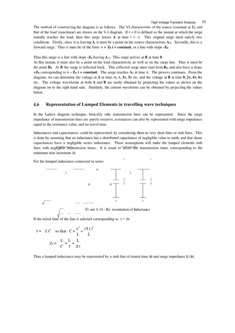
8/6/2019 High Voltage Engineering (Lucas)
http://slidepdf.com/reader/full/high-voltage-engineering-lucas 69/212
High Voltage Transient Analysis
The method of constructing the diagram is as follows. The VI characteristic of the source (constant at E), andthat of the load (non-linear) are drawn on the V-I diagram. If t = 0 is defined as the instant at which the surgeinitially reaches the load, then this surge leaves A at time t = - 2. This original surge must satisfy twoconditions. Firstly, since it is leaving A, it must be a point on the source characteristic A-1. Secondly, this is aforward surge. Thus it must be of the form v + Z 0 i = constant , or a line with slope -Z 0.
Thus this surge is a line with slope -Z 0 leaving A-1. This surge arrives at B at time 0.At this instant, it must also be a point on the load characteristic as well as on the surge line. Thus it must bethe point B0. At B the surge is reflected back. This reflected surge must start from B0, and also have a slope+Z 0 corresponding to v - Z 0 i = constant . The surge reaches A1 at time 2 . The process continues. From thediagram, we can determine the voltage at A at time -2 , 2 , 32 , 52 etc, and the voltage at B at time 0, 2 2 , 4 2 , 6 2 etc. The voltage waveforms at both A and B are easily obtained by projecting the values as shown on thediagram on to the right hand side. Similarly, the current waveforms can be obtained by projecting the valuesbelow.
Representation of Lumped Elements in travelling wave techniques
In the Lattice diagram technique, basically only transmission lines can be represented. Since the surgeimpedance of transmission lines are purely resistive, resistances can also be represented with surge impedanceequal to the resistance value, and no travel time.
Inductances and capacitances could be represented, by considering them as very short lines or stub lines. Thisis done by assuming that an inductance has a distributed capacitance of negligible value to earth, and that shuntcapacitances have a negligible series inductance. These assumptions will make the lumped elements stublines with negligible transmission times. It is usual to select the transmission times corresponding to the
minimum time increment ûW
For the lumped inductance connected in series
If the travel time of the line is selected corresponding to 2 ûW
Thus a lumped inductance may be represented by a stub line of transit time û Wand surge impedance / û W.
FFFFF FFFFF ≡ FFNFF FFNFFF L G L G
G G FOF C FOF CFNF 2 FNF 2
G G G G G G
FOF FOF F F
Fi ure 4.14 - Re resentation of Inductance
tL
=L
=CL
=Z
L)t(
=L
=C thatso
0
22
∆
∆
τ
τ τ C L=

8/6/2019 High Voltage Engineering (Lucas)
http://slidepdf.com/reader/full/high-voltage-engineering-lucas 70/212
High Voltage Engineering - J R Lucas, 2001
For the lumped capacitance connected in shunt
Thus a lumped capacitance may be represented by a stub line of transit time û Wand surge impedance û W &.
Another method of analyzing in the presence of inductances and capacitances is to use the numerical form asindicated below.
4.7 Branch Time Table for digital computer implementation
The Bewley Lattice diagram cannot be implemented directly on the digital computer. When implemented onthe computer, a physical diagram is not required to keep track of the travelling waves. The branch time tableserves the purpose of the diagram, and keeps track of the voltage of each node, and the reflected andtransmitted waves.
G ≡ FFF FFFNFFF FFF FOF C L G LFNF 2 G 2
G FOF C
FNF G G
FOF F
Fi ure 4.15 - Representation of Capacitance
Ct
=C
=CL
=Z
C)t(
=C
=L thatso
0
22
∆
∆
τ
τ τ C L=
vL2t
+i=I where
I+vL2t
=i also
itL2
+v-itL2
=v .e.i
ti-i L=
2v+v
inductanceanfor
eq
1n-eq,nn
1n-1n-nn
1n-n1n-n
∆
∆
∆∆
∆
t d id
L=v
tC2
-i-=I where
I+vt
C2 =i .e.i
vt
C2 +i-v
tC2
=i .e.it
v-v C=2
i+i
ecapacitancanfor
eq
1n-eq,nn
1n-1n-nn
1n-n1n-n
∆
∆
∆∆∆
t d vd
C =i

8/6/2019 High Voltage Engineering (Lucas)
http://slidepdf.com/reader/full/high-voltage-engineering-lucas 71/212
High Voltage Transient Analysis
4.8 Transform Methods of solving Transients
Simple transient problems may be solved using the Laplace Transform. However, since its inverse transformis not evaluated for complicated transforms, the Fourier transform is preferred. Further, for digital computerapplication, what is used is the numerical form of the transform, which is obtained by approximating theintegrals to summations.
This is used with the transfer function H( &) of a network to give the transform of the response.
R(&) = H( &) . F( &)
The response in the time domain is then obtained by inverse transformation.
With the approximations introduced, the period of observation T and the maximum frequency are limited tofinite values.
The transmission line is usually represented by the frequency dependant two-port admittance parameters, forthe determination of the transfer function.
whereA = Y 0 coth lB = Y 0 cosech lY0 = surge impedance matrix
= propagation matrix
t e(t) f = dt e(t) f =)F( t j-T
0
t j-
0
∆∑∫ ∞
ω ω ω
HFFFFFFFFFFI FFF>FFFM H( &) LFFF>FFF
F( &) JFFFFFFFFFFK R( &)
Fi ure 4.16 - Block dia ram of system
ω ω π
ω ω π
ω
ω
.e.) R(2
=r(t)
d .e.) R(2
=r(t)
t j
0
t j
0
∆∑
∫
Ω
∞
H I H IH I G I G G A -B GG V G G S G G GG S G G G G GG G G G = G GG G G I G G -B A GG V G G R G G GG S G J K J KJ K

8/6/2019 High Voltage Engineering (Lucas)
http://slidepdf.com/reader/full/high-voltage-engineering-lucas 72/212

8/6/2019 High Voltage Engineering (Lucas)
http://slidepdf.com/reader/full/high-voltage-engineering-lucas 73/212
High Voltage Cables
5.1.1 Dielectric loss
For a perfect dielectric, the power factor is zero. Since the cable is not a perfect dielectric, the power factor isnot zero. The current leads the voltage by an angle of less than 90 o, and hence there is a power loss (Figure5.3).
If C is the capacitance of the cable, and E is the applied voltage, then
charging current i = E C & power loss P = E I cos 3 ( , VLQ/
= E (i/cos / VLQ/ (2 C & WDQ/
The power loss is proportional to E 2 and tan /
5.1.2 Conductor loss
The conductor loss P c is given byPc = I2 Rc watt
where R c is the resistance of the conductor and I is the current in the cable.
5.1.3 Sheath loss
The losses occurring in the sheath of a cable is usually obtained by the empirical formula of Arnold. Arnold'sformula for the sheath loss P sh is given by
where r m = mean radius of sheathd = distance between cables (centre to centre)Rsh = resistance of full length of cableI = current in cable
The sheath loss is usually about 2 to 5 % of the conductor loss.
5.1.4 Intersheath Loss
Intersheath losses are caused by the induced emf between the sheaths causing a circulating current.This loss is thus present only when the sheaths of adjacent cables are connected together. The sheaths need tobe connected together in practice, as otherwise sparking could occur causing damage to the sheaths. Theintersheath loss P ish can be calculated as follows.
The mutual inductance M sh between a core of one cable and the sheath of an adjacent cable is given by
The voltage induced E ish is given byEish = I . & 0sh
G , G
G
G
G /
G 3
JFFFFFFFFFFFFFFFFFFF ¾ E
Fi ure 5.3 - Loss an le
watt d r
R I 10 x7.7 =P
m2
sh
23-
sh
r d
2 = M sh lnπ µ
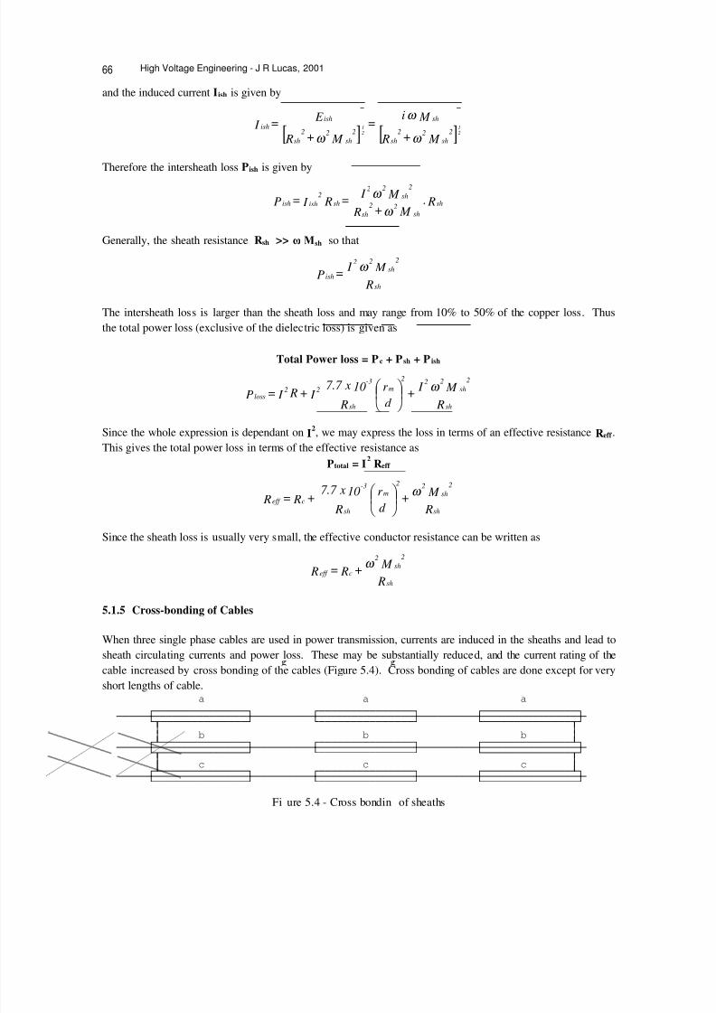
8/6/2019 High Voltage Engineering (Lucas)
http://slidepdf.com/reader/full/high-voltage-engineering-lucas 74/212
High Voltage Engineering - J R Lucas, 2001
and the induced current I ish is given by
Therefore the intersheath loss P ish is given by
Generally, the sheath resistance R sh >> & 0 sh so that
The intersheath loss is larger than the sheath loss and may range from 10% to 50% of the copper loss. Thusthe total power loss (exclusive of the dielectric loss) is given as
Total Power loss = P c + P sh + P ish
Since the whole expression is dependant on I 2, we may express the loss in terms of an effective resistance R eff .This gives the total power loss in terms of the effective resistance as
P total = I2
R eff
Since the sheath loss is usually very small, the effective conductor resistance can be written as
5.1.5 Cross-bonding of Cables
When three single phase cables are used in power transmission, currents are induced in the sheaths and lead tosheath circulating currents and power loss. These may be substantially reduced, and the current rating of thecable increased by cross bonding of the cables (Figure 5.4). Cross bonding of cables are done except for veryshort lengths of cable.
[ ] [ ] M + R
M i =
M + R
E = I sh
22sh
2 sh
sh22
sh2
ishish
21
21
ω
ω
ω
R. M + R
M I = R I =P shsh
2sh
2sh
222
shish2
ishω
ω
R M I =Psh
sh222
ishω
R M I +
d r
R10 x7.7
I + R I =Psh
sh222
m2
sh
-322
lossω
R M +
d r
R10 x7.7
+ R= Rsh
sh22
m2
sh
-3
ceff ω
R M + R= R
sh
sh22
ceff ω
a a aHFFFFFFFFFFFFFFFI HFFFFFFFFFFFFFFFI HFFFFFFFFFFFFFFFI FFFFFFFFFFFFFFFFFFFFFFFFFFFFFFFFFFFFFFFFFFFFFFFFFFFFFFFFFFFFFFFFFFFFFFFFFFFF JNFFFFFFFFFFFFFFK JFFFFFFFFFFFFFFFK JFFFFFFFFFFFFFFNK G G
G b b b G HOFFFFFFFFFFFFFFI HFFFFFFFFFFFFFFFI HFFFFFFFFFFFFFFOI FFFFFFFFFFFFFFFFFFFFFFFFFFFFFFFFFFFFFFFFFFFFFFFFFFFFFFFFFFFFFFFFFFFFFFFFFFFF JNFFFFFFFFFFFFFFK JFFFFFFFFFFFFFFFK JFFFFFFFFFFFFFFNK G G G c c c G HOFFFFFFFFFFFFFFI HFFFFFFFFFFFFFFFI HFFFFFFFFFFFFFFOI
FFFFFFFFFFFFFFFFFFFFFFFFFFFFFFFFFFFFFFFFFFFFFFFFFFFFFFFFFFFFFFFFFFFFFFFFFFFF
JFFFFFFFFFFFFFFFK JFFFFFFFFFFFFFFFK JFFFFFFFFFFFFFFFK Fi ure 5.4 - Cross bondin of sheaths

8/6/2019 High Voltage Engineering (Lucas)
http://slidepdf.com/reader/full/high-voltage-engineering-lucas 75/212
High Voltage Cables
The continuity of each cable sheath is broken at regular intervals; the cables between two adjacentdiscontinuities being a minor section. 3 minor sections make up a major section, where the sheaths are solidlybonded together and to earth. A residual sheath voltage exists, and the desired balance, giving negligiblesheath voltage between the solid grounded positions is achieved by transposing the cables at each cross-
bonded section. To prevent excessive voltage build up at the cross bonded points, especially during faults,these points are earthed through non-linear resistors which limit voltage build up. The cable is alsotransposed. (Figure 5.5)
5.2 Impregnated Paper Insulation
The insulation consists mainly of paper tape impregnated with compound. The paper must be free fromligneous fibres and from metallic or other conducting spots. The compound with which the paper is insulated
should be of such a consistency that it is plastic at ordinary temperatures, and has no tendency to drain awayfrom the cable.
The impregnating compound varies from manufacturer to manufacturer,but they all are based o paraffinic ornaphthenic mineral oil, with resin frequently added to lower the viscosity and to improve its impregnatingqualities. The paper is made from Manila fibre or wood pulp.
Impregnated paper can withstand an electric stress if about 5 to 10 times that which could be withstood by drypaper insulation. The dielectric strength of impregnated paper is about 200 to 300 kV/cm. Initially, they maybe able to withstand about 400 to 600 kV/cm. The cause of breakdown is usually the non-homogeneity of thedielectric. When a test voltage is applied, the weakest part of the dielectric breakdown and deterioration startsgetting more and more. This is accentuated by the fact that the cable is not carrying the same current all thetime. The deterioration results in the formation of voids and gasses. When the voltage is raised, ionisation orglow discharge can occur in the voids and ionic bombardment of thee surface. Some of the oil sufferscondensation and hydrogen and other gases are evolved. Thus the long term breakdown strength and theinstantaneous break down strengths differ. This value may decrease with time due to deterioration to about160 to 200 kV/cm. In the case of a badly impregnated dielectric, the breakdown stress will continue todecrease and ultimately leads to breakdown. With the use of a safety factor, not more than about 40 kV/cm isallowed in service (Figure 5.6).
a HFFFFFFFFFFFFI a HFFFFFFFFFFFFI aHFFFFFFFFFFFFFFOI HOFFFFFFFFFFFFFOI HOFFFFFFFFFFFFFFI FFFFFFFFFFFFFFFFFFFFFF FFFFFFFFFFFFFFFFFFFFF FFFFFFFFFFFFFFFFFFFFF JNFFFFFFFFFFFFFFK JNFFFFFFFFFFFFFNK JFFFFFFFFFFFFFFNK G L L G G M M G G FOF FOF G G F F G
G b HFFFFFFFFFFFFFI b HFFFFFFFFFFFI b G HOFFFFFFFFFFFFFOI HOFFFFFFFFFFFFFOI HOFFFFFFFFFFFFFOI FFFFFFFFFFFFFFFFFFFFFF FFFFFFFFFFFFFFFFFFFF FFFFFFFFFFFFFFFFFFFFF JNFFFFFFFFFFFFFFK JNFFFFFFFFFFFFFNK JFFFFFFFFFFFFFFNK G L L G G M M G G FOF FOF G G F F G
G c HFFFFFFFFFFFFFI c HFFFFFFFFFFFI c G HOFFFFFFFFFFFFFOI HOFFFFFFFFFFFFFOI HOFFFFFFFFFFFFFOI FFFFFFFFFFFFFFFFFFFFFF FFFFFFFFFFFFFFFFFFFFF FFFFFFFFFFFFFFFFFFFFF JNFFFFFFFFFFFFFFK JNFFFFFFFFFFFFFNK JFFFFFFFFFFFFFFNK G L L G G M M G FOF FOF FOF FOF F F F F
Fi ure 5.5 - Non-linear resistor earthin

8/6/2019 High Voltage Engineering (Lucas)
http://slidepdf.com/reader/full/high-voltage-engineering-lucas 76/212
High Voltage Engineering - J R Lucas, 2001
5.2.1 Properties required of cable insulation
Dielectrics used for cable insulation must have the following properties.
1. High Insulation resistance2. High dielectric strength3. Good mechanical strength4. Immune to attack by acids and alkali in the range 0 - 100 o C5. Should not be too costly6. Should not be hygroscopic (tending to absorb water), or if hygroscopic should be enclosed in a
water tight covering.
5.2.2 Principle underlying the design of high voltage cable insulation
By means of dielectric tests on cables, it has been observed that the long term breakdown stress is increased if the cable is subjected to pressure. This is due to the fact that the pressure discourages the formation of voids.Even for a badly impregnated cable, the application of pressure improves the power factor (or loss tangent)
considerably. If the cable is subjected to a pressure of about 15 atmospheres, the long term dielectric strengthimproves to about 400 kV/cm and a working stress of about 150 kV/cm may be used (Figure 5.7).
¿ b.d.v. 500 M
G 400 M F F F F F F F F F F F F F F F F F F under pressure
G (15 atmospheres) 300 M G 200 M F F F F F F F F F F F F F F F F F F without pressure
G 100 M
G 0 OFFFFFFFFFFFFFFFFFFFFFFFFFFFFFFFFFFFFFFFFFFFF¾
time (hrs)Fi ure 5.6 - Breakdown volta e characteristic of paper insulation
¿ ¿ tan / G breakdown M
G stress G G G G G G 400 M G
G (kV/cm) G (a)G G (b) G G G 300 M (b)G G G G G G G G (a) 200 M (c)G G G G (c) G G
0.01 M 100 M G G G G G Applied stress G timeLFFFNFFFNFFFPFFFNFFFNFFFF¾ 0 OFFFFFFFFFFFFFFFFFFFOFFFFFF¾ 0 20 40 60 80 100 kV/cm 100 (hrs)
(a) impregnated ( 1 atmos) (a) 15 atmospheres(b) badly impregnated ( 1 atmos) (b) 8 atmospheres(c) badly impregnated (15 atmos) (c) 1 atmosphere
Fi ure 5.7 - Variations with pressure

8/6/2019 High Voltage Engineering (Lucas)
http://slidepdf.com/reader/full/high-voltage-engineering-lucas 77/212
High Voltage Cables
Comparison of the curves for (a) well impregnated cable at atmospheric pressure, (b) badly impregnated cableat atmospheric pressure, and (c) badly impregnated cable at a pressure of 15 atmospheres for about 47 hours,shows the advantages of the pressure on the reduction of power factor. Further the curves show how the longterm breakdown stress is improved by pressure.
In modern high voltage cables, with the use of better materials, the power factor has been reduced from about(0.007 to 0.01) to about (0.002 to 0.003).
For high voltage cables, impregnated paper insulation is very commonly used. The paper is porous andcontains in itself the impregnating compound. There are no voids present as the oil is present between thelayers of the paper which forms the insulation.
5.2.3 Paper insulated power cables
The conductor of the cable is stranded, and this is lapped round with the paper tape. It is first heated to about100 oC taking care not to burn it. A vacuum is then applied for 20 to 50 hours to get rid of any trapped airinside the cable, and while still under vacuum, impregnating compound is poured into the tank and thereafter apressure of 50 p.s.i. (about 0.35 MN/m 2) is applied. Impregnating of the paper prevents void formation in thedielectric, as voids can easily lead to the breakdown of the dielectric. As paper is hygroscopic, a seamlesslead sheath is extruded over the insulation so that no moisture will get in.
For high voltages, pressurised cables are used where the impregnated paper insulation is kept under pressure.A pressure of about 15 atmospheres is applied so that any potential voids would be instantaneously filled.The pressure may be applied by having either oil or gas under pressure. When the cable is pressurised,longitudinal reinforcement to prevent bulging and reinforcement to prevent hoop stress are used. Withpressurised cables, the long term breakdown strength does not differ much from the short term strength, and assuch using a safety factor, a working stress of about 100 to 120 kV/cm may be used.
5.2.4 Insulation Resistance
For a single core cable (figure 5.8), the insulation resistance between the conductor and the outer sheath isgiven by the following.
R
x û[ r
Fi ure 5.8 - Cable cross-section
(km)cableof length=lwhere
M10x)rR
(logl
3.665 =Res.e.i
)rR
ln(l2
=x
dxl2
=Res=Res
(m)cableof length=lwhere
10-10
R
r
′
Ω′
∆∫ ∴
∆∆
∫ ρ
π ρ
π ρ
π ρ
l x2 x.
= Res

8/6/2019 High Voltage Engineering (Lucas)
http://slidepdf.com/reader/full/high-voltage-engineering-lucas 78/212
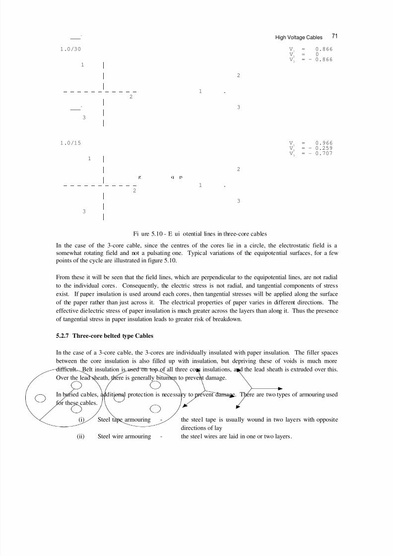
8/6/2019 High Voltage Engineering (Lucas)
http://slidepdf.com/reader/full/high-voltage-engineering-lucas 79/212

8/6/2019 High Voltage Engineering (Lucas)
http://slidepdf.com/reader/full/high-voltage-engineering-lucas 80/212
High Voltage Engineering - J R Lucas, 2001
Capacitance of 3-core belted type
The capacitance between the conductor to neutral of 3-core beltedcables (Figure 5.11) cannot be obtained by a simple derivation asfor the single core cable. Simon's expression can be used toobtain this value.
The capacitance per unit length to neutral is given by
If t = thickness of belt insulationT = thickness of conductor insulationd = diameter of conductor0r = dielectric constant
Measurement of capacitance of 3-core cables
In three-core cables, capacitance does not have a single value, but can belumped as shown in figure 5.12.
Capacitance between each core and sheath = C s
Capacitance between cores = C
These can be separated from measurements as described in the followingsection.
(a) Strap the 3 cores together and measure the capacitancebetween this bundle and the sheath as shown in figure5.13.
Measured value = C m1 = 3 C s
This gives the capacitance to the sheath as C s = C m1 /3
(b) Connect 2 of the cores to the sheath and measurebetween the remaining core and the sheath (Figure 5.14).
Measured value C m2 = 2 C + C s
i.e. C = (C m2 - C s)/2 = (3 C m2 - C m1)/6
which gives the capacitance between the conductors.
conductor
Sheath
Figure 5.11 - 3 core belted cable
F/km
log
µ ε
1+d
t +T 3.84+T t 1.7 -
T t 0.52
0.03 =C
2
10
r 0
Fi ure 5.12 - Cable Capacitances
----------- I G
HFFFFFFFFI G --- M%ULGJH L- K
JFFFFFFFFK
Figure 5.13 - Capacitance measurement
F F F F F FI HFFFFFFFFI G
FM%ULGJH L F K JFFFFFFFFK
Figure 5.14 - Capacitance measurement
C s
C s C s
C
C C
C s
C s C s
C s
C
C C
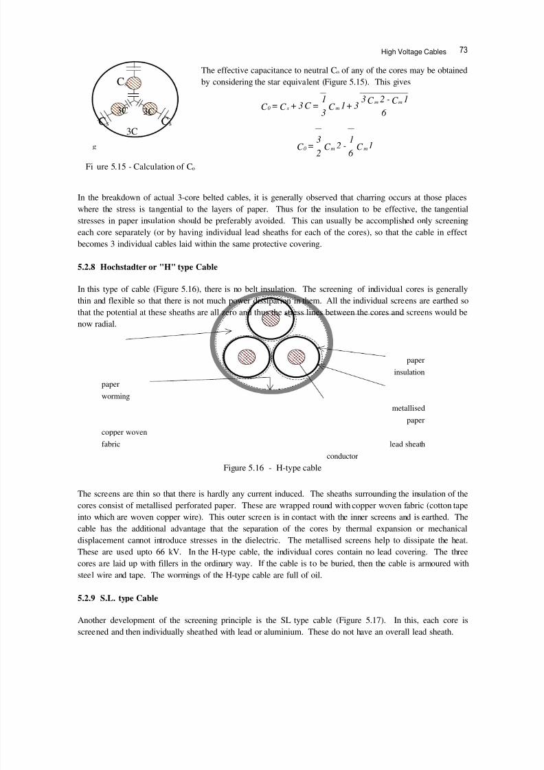
8/6/2019 High Voltage Engineering (Lucas)
http://slidepdf.com/reader/full/high-voltage-engineering-lucas 81/212
High Voltage Cables
The effective capacitance to neutral C o of any of the cores may be obtainedby considering the star equivalent (Figure 5.15). This gives
In the breakdown of actual 3-core belted cables, it is generally observed that charring occurs at those placeswhere the stress is tangential to the layers of paper. Thus for the insulation to be effective, the tangentialstresses in paper insulation should be preferably avoided. This can usually be accomplished only screeningeach core separately (or by having individual lead sheaths for each of the cores), so that the cable in effectbecomes 3 individual cables laid within the same protective covering.
5.2.8 Hochstadter or "H" type Cable
In this type of cable (Figure 5.16), there is no belt insulation. The screening of individual cores is generallythin and flexible so that there is not much power dissipation in them. All the individual screens are earthed sothat the potential at these sheaths are all zero and thus the stress lines between the cores and screens would benow radial.
The screens are thin so that there is hardly any current induced. The sheaths surrounding the insulation of thecores consist of metallised perforated paper. These are wrapped round with copper woven fabric (cotton tapeinto which are woven copper wire). This outer screen is in contact with the inner screens and is earthed. Thecable has the additional advantage that the separation of the cores by thermal expansion or mechanicaldisplacement cannot introduce stresses in the dielectric. The metallised screens help to dissipate the heat.These are used upto 66 kV. In the H-type cable, the individual cores contain no lead covering. The threecores are laid up with fillers in the ordinary way. If the cable is to be buried, then the cable is armoured withsteel wire and tape. The wormings of the H-type cable are full of oil.
5.2.9 S.L. type Cable
Another development of the screening principle is the SL type cable (Figure 5.17). In this, each core isscreened and then individually sheathed with lead or aluminium. These do not have an overall lead sheath.
Fi ure 5.15 - Calculation of C o
1C 6 1
-2C 23
=C
6
1C -2C 3 3+1C
31
=C 3+C =C
mm0
mmms0
paper
insulation
paper
worming
metallised
paper
copper woven
fabric lead sheath
conductor
Figure 5.16 - H-type cable
C s
C s C s3C
3C 3C

8/6/2019 High Voltage Engineering (Lucas)
http://slidepdf.com/reader/full/high-voltage-engineering-lucas 82/212
High Voltage Engineering - J R Lucas, 2001
The electric field in the insulation surrounding each core is naturally radial and the function of the screens inthis case is to eliminate the possibility of any stress across the clearance space between core and sheath. Thewormings of the filler spaces in the S.L. type cables do not contain much oil as do not get any electric stress.
The three metal sheathed cores, after being lapped with paper and cotton tapes are laid with tarred jute yarn toget a circular formation and then wrapped with hessian tapes to form a bedding for the armouring. Theelectrical and thermal advantages of H-type cables are also enjoyed by the S.L. type cables. These cables aresuitable for hilly routes, as the absence of oil in the filler spaces lessens the risk of oil drainage. Also, the S.L.type construction is useful on short runs because the terminating equipment is simplified. Also the voidformation in the filler spaces are of no consequence. The separate lead sheaths in the S.L. cable are the seatsof induced currents, but the resulting losses are small, and appear to be of no practical significance.
5.2.10 Copper Space Factor
Unlike in overhead lines, insulation in cables occupies a greater portion of the cable space. Thus higherinstallation costs are involved. Ideally we would like the insulation to occupy the minimum possiblethickness. Thus we define a space factor to indicate the utilisation of the space. The copper space factor isdefined as
copper space factor = cross-section area of conductorcross-section area of whole cable
For a single core cable, the best space factor is obtained with a concentricarrangement (Figure 5.18), as this gives the minimum conductor perimeter for thegreatest conductor area and given insulation thickness. Thus
Space factor = r 2 /R2
For the 3-core cable (Figure 5.19), consisting of circular conductors withina circular sheath,
Space factor = 3 r 2 /R2
where T = thickness of core insulation, t = thickness of belt insulation
and R 1 = r + T
However, for the 3-core cable the circular cross-section is not the bestshape for the conductors.
core
insulation
compound jute worming
cotton
tape
lead sheath core
Figure 5.17 - S L type cable
Fi ure 5.18
Fi ure 5.19 - three-core cable
R
r
R
r
T
t

8/6/2019 High Voltage Engineering (Lucas)
http://slidepdf.com/reader/full/high-voltage-engineering-lucas 83/212
High Voltage Cables
Other shapes which gives better space factors are the elliptical shaped conductors and the sector shapedconductors (Figure 5.20).
5.3 Dielectric Stress in a Single Core Cable
The voltage difference across the conductor and the sheath of a single core cable is given by
It is seen that since x is the only variable, the maximum stress in the dielectric occurs at the minimum value of the radius x (i.e. x = r).
Since it is required that this maximum stress in the dielectric should be as low as possible, differentiating with
respect to r for minimum max gives
Thus if the overall diameter of the cable is kept fixed, then R/r = e is the condition for minimum max . Thisvalue of radius of conductor will generally be larger than would be required for current carrying capacity.
Figure 5.20 - Special shapes of conductors to give better space factors
rR logx
v = thatso
x2
q = ,alsolog
e
x
x
ξ
ε π ξ
ε π ,
r R
2q
=v e
rR
logr
V = .e.i
e
maxξ
2.718=e=r
R .e.i
0=r1
-.r+rR
log.R/rlogr
V .e.i e
e
2
max
0=r d
d ξ
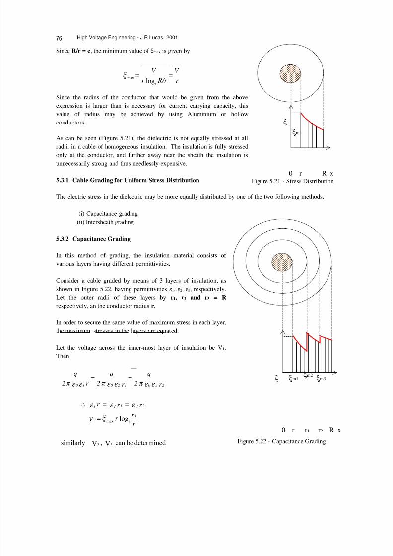
8/6/2019 High Voltage Engineering (Lucas)
http://slidepdf.com/reader/full/high-voltage-engineering-lucas 84/212
High Voltage Engineering - J R Lucas, 2001
Since R/r = e , the minimum value of max is given by
Since the radius of the conductor that would be given from the aboveexpression is larger than is necessary for current carrying capacity, thisvalue of radius may be achieved by using Aluminium or hollowconductors.
As can be seen (Figure 5.21), the dielectric is not equally stressed at allradii, in a cable of homogeneous insulation. The insulation is fully stressedonly at the conductor, and further away near the sheath the insulation isunnecessarily strong and thus needlessly expensive.
5.3.1 Cable Grading for Uniform Stress Distribution
The electric stress in the dielectric may be more equally distributed by one of the two following methods.
(i) Capacitance grading(ii) Intersheath grading
5.3.2 Capacitance Grading
In this method of grading, the insulation material consists of various layers having different permittivities.
Consider a cable graded by means of 3 layers of insulation, asshown in Figure 5.22, having permittivities 01, 02, 03, respectively.Let the outer radii of these layers by r 1, r 2 and r 3 = R respectively, an the conductor radius r .
In order to secure the same value of maximum stress in each layer,the maximum stresses in the layers are equated.
Let the voltage across the inner-most layer of insulation be V 1.Then
Figure 5.21 - Stress Distribution
r V =
R/r r V
=elogmaxξ
Figure 5.22 - Capacitance Grading
r = r = r
r 2q
=r 2
q =
r 2q
23121
23012010
ε ε ε
ε ε π ε ε π ε ε π
∴
determinedbecanV ,V similarly
log
32
max
r r r =V
1e1 ξ
R x r
ξ
ξm
0
ξ ξm1ξm2 ξm3
R x r r1 r20

8/6/2019 High Voltage Engineering (Lucas)
http://slidepdf.com/reader/full/high-voltage-engineering-lucas 85/212

8/6/2019 High Voltage Engineering (Lucas)
http://slidepdf.com/reader/full/high-voltage-engineering-lucas 86/212
High Voltage Engineering - J R Lucas, 2001
In the particular case that all the n layers have the same thickness d , and if r is the conductor radius,
r1 = r + d; r 2 = r + 2d; r 3 = r + 3d; ....... r n = r + n d
The voltage across the m th section is given by
Hence substituting for the different values of m , we can obtain the voltage across the various layers that haveto be maintained to give equal maximum stress in each section.
In practice, there is a considerable difficulty in arranging for many intersheaths, this difficulty being mainlyassociated with the provision of the different voltages for the intersheaths, and as a result it is usual to design acable of this type with only one intersheath.
This simplifies the design calculations, and the expression for the maximum stress then given by
For the purpose of comparison with the ungraded cable, let us first take the optimally designed ungraded cable(i.e. with R/r = e ), and introduce an intersheath at a radius r 1. Since R and r are both kept fixed, r 1 is the onlyvariable, and the expression for stress must be differentiated with respect to r 1 to obtain the condition for theminimum value of the maximum stress.
This gives the solution r 1 = 1.76 r .
( )d1)-(m+r
dm+rlogd1)-(m+r=M where
loglog
e
n
1=m
max
∑
M
V =.....=
d +r d 2+r d)+(r
V =
r d +r r
V =
e
2
e
1ξ
[ ]d 1)-(m+r
d m+r d 1)-(m+r
M V
=V em log
r r r +
r
R r
V =1
e1
e1 loglogmaxξ
1=rr log
rr
1=elog also e,=rR
gconsiderin
0=r
r +r
R log+1- .e.i
1e
1
e
11e
∴
0=r1
.r
r .r+
r
R log+
r
R- .
Rr .r thatso
11e
12
11
max
∂∂
0=r 1
ξ

8/6/2019 High Voltage Engineering (Lucas)
http://slidepdf.com/reader/full/high-voltage-engineering-lucas 87/212
High Voltage Cables
However, for the cable without intersheath, we have max = V/r . Hence, the addition of the intersheath raisesthe maximum applicable voltage by 33% .
Now let us consider the case of only the overall diameter of the cable R being fixed, and both r and r 1 beingvariable. Then for minimum value of the maximum stress we have
5.4 Pressurised High Voltage Cables
In high voltage paper insulated cables, the application of pressure (about 13 atmospheres) increases themaximum allowable working stress (after applying a suitable safety factor) from about 50 kV/cm to about 150
kV/cm.
In super voltage cables, the void control is effected by pressurising the oil-impregnated paper tape insulationby (a) pressurising the oil, and (b) applying gas pressure.
5.4.1 Oil-pressure cables
In oil filled cables, the oil must be free to flow inorder to transmit the pressure. The maximum pressure of oilutilised is about 0.35 MN/m 2 (3.5 atmospheres or 50 p.s.i.). Due to the pressure of oil, the sheath tends tobulge out and therefore reinforcement of the sheathing is necessary. A reservoir maintains the requiredpressure. The cable can now operate at a maximum working stress of 150 kV/cm.
In normal, solid type of cable, the drying and impregnating are done before sheathing, while in oil-filled cablesthey can be done after sheathing by circulating hot oil. The oil filled construction permits a great reduction insize of the cable.
r 1.33V
=
r r 1.76
r +r 1.76
r e r 1.76
V =
ee
∴
loglogmaxξ
1.881=r
R giving
e1
-1=r
R log givesThis
0=e1
+r
R log+1- e,=
rr .e.i
0=r
r +r
R log+1- also 0,=1-r
r log .e.i
11e
1e
1
11e
1
e
maxmax 0=r
0,=r 1∂
∂∂
∂ ξ ξ
r2.718V
= .e.i
loglog
max
max
ξ
ξ
r eV
=
r +e1
-1r e
V =
er +r
R r e
V =
e1
e

8/6/2019 High Voltage Engineering (Lucas)
http://slidepdf.com/reader/full/high-voltage-engineering-lucas 88/212
High Voltage Engineering - J R Lucas, 2001
There are 3 main types of oil filled cables. These are (a) single-core, conductor channel; (b) single-core,sheath channel; and (c) three-core, filler-space channels.
(a) Single-core conductor channel
This type of cable shown in figure 5.24 has a hollow conductor which acts as an oil channel, and is thesimplest from the point of view of the cable itself. A disadvantage of this arrangement is that the oil is at highvoltage with respect to earth being at the voltage of the conductor. The copper strands of which the conductoris made are laid over a helical metal ribber, so that oil can reach the insulation.
(b) Single-core sheath channel
In this type (Figure 5.25), the oil channels are produced either by grooving the sheath or by arranging spacersbetween sheath and insulation. The resistance to oil flow in this type is 6 to 8 times that of type (a), so thatmore feeding points are necessary to maintain the pressure. An advantage is that the channels are at earth
potential so that joints and installation are simpler.
(c) Three-core, filler space channels
Oil duct Lead sheath
hollowconductor
helical ribbon
paper reinforcementinsulation
Figure 5.24 - Single core conductor channel cable
oil lead sheathgrooved channelsleadsheath
button-stampedpaper helical
insulation spacer ribbon
Figure 5.25 - Single core sheath channel cable
lead sheath paper insulation
paper filler perforated oil-ducts
Figure 5.26 - Three core filler space channel cable
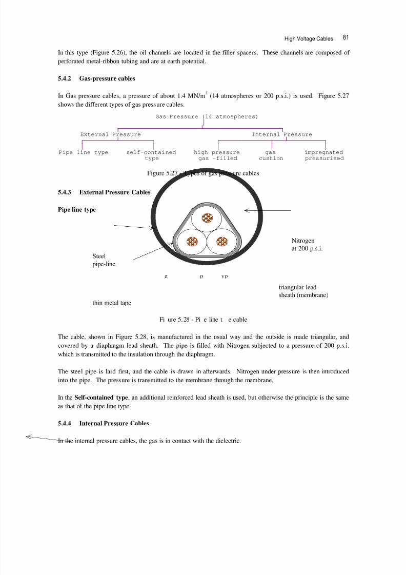
8/6/2019 High Voltage Engineering (Lucas)
http://slidepdf.com/reader/full/high-voltage-engineering-lucas 89/212
High Voltage Cables
In this type (Figure 5.26), the oil channels are located in the filler spacers. These channels are composed of perforated metal-ribbon tubing and are at earth potential.
5.4.2 Gas-pressure cables
In Gas pressure cables, a pressure of about 1.4 MN/m 2 (14 atmospheres or 200 p.s.i.) is used. Figure 5.27shows the different types of gas pressure cables.
5.4.3 External Pressure Cables
Pipe line type
The cable, shown in Figure 5.28, is manufactured in the usual way and the outside is made triangular, andcovered by a diaphragm lead sheath. The pipe is filled with Nitrogen subjected to a pressure of 200 p.s.i.
which is transmitted to the insulation through the diaphragm.
The steel pipe is laid first, and the cable is drawn in afterwards. Nitrogen under pressure is then introducedinto the pipe. The pressure is transmitted to the membrane through the membrane.
In the Self-contained type , an additional reinforced lead sheath is used, but otherwise the principle is the sameas that of the pipe line type.
5.4.4 Internal Pressure Cables
In the internal pressure cables, the gas is in contact with the dielectric.
Gas Pressure (14 atmospheres)G
HFFFFFFFFFFFFFFFFFFFFFFFOFFFFFFFFFFFFFFFFFFFFFFI External Pressure Internal PressureHFFFFFFFFFOFFFFFFFFFI HFFFFFFFFFFFFFFNFFFOFFFFFFFFFFI G G G G G
Pipe line type self-contained high pressure gas impregnatedtype gas -filled cushion pressurised
Figure 5.27 - Types of gas pressure cables
Nitrogenat 200 p.s.i.
Steel
pipe-line
triangular leadsheath (membrane)
thin metal tape
Fi ure 5.28 - Pi e line t e cable
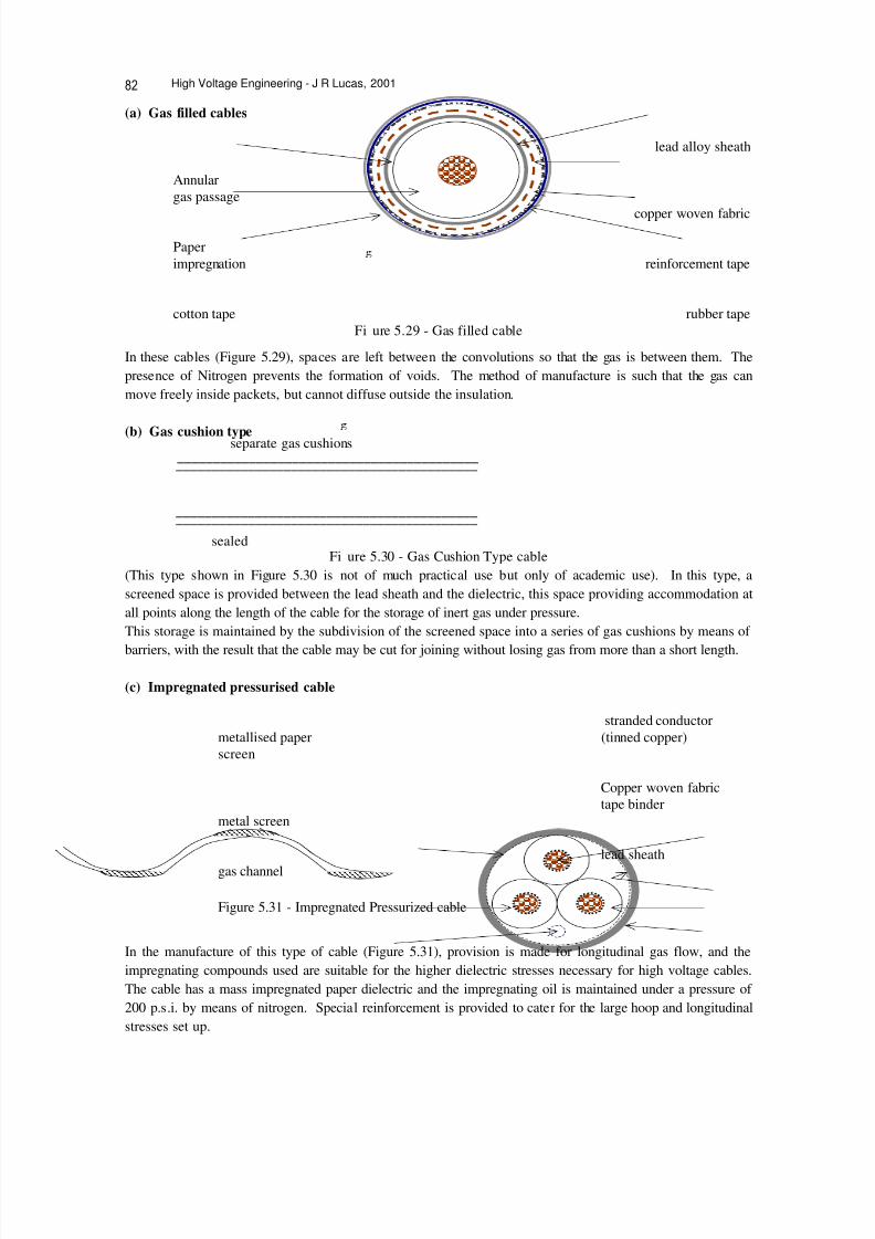
8/6/2019 High Voltage Engineering (Lucas)
http://slidepdf.com/reader/full/high-voltage-engineering-lucas 90/212

8/6/2019 High Voltage Engineering (Lucas)
http://slidepdf.com/reader/full/high-voltage-engineering-lucas 91/212
High Voltage Cables
The core is stranded and is covered with a metallised paper screen so as to obtain a completely uniform stress.The gas channel is in one of the filler spaces.
5.5 Thermal Design of Cables
Underground cables are installed in trenches of rectangular cross-section. After excavation of the trench, alayer of sand is placed in it to serve as a bedding, as shown in Figure 5.32.
The length of cable is pulled in along the trench and covered with a further layer of sand. Sand free from flintsand stone is employed to avoid damage to the cable serving during pulling and initial back filling. Above thecable and sand bedding are placed cover tiles to protect the cable from mechanical damage from subsequentexcavation activities. The excavated material is replaced in the trench and stamped to consolidate it. Theminimum trench width that can be conveniently excavated is about 700 mm (27 inches), and for safety reasons,the minimum depth of burial in normal circumstances is 900 mm (36 inches).
An underground cable carrying current will have in addition to the conductor loss, dielectric loss and losses inthe sheath. These produce heat which are conducted away from the cable to the surface, producing atemperature gradient.
When more than one single core cable is laid together (as is required for three phase systems exceeding 150kV), the heat produced by one conductor affects the other and the heat factors need to be modified. When thespacing between the cables is increased, the heat produced by the circulating currents between the cables will
increase whereas the eddy current losses decrease. Thus there is an optimum spacing for cables and variousalternatives may have to be evaluated before the economic arrangement is finally selected.
5.5.1 Current rating of Cables
In a cable, the factor which ultimately limits the current carrying capacity is the maximum operatingtemperature which may be sustained by the cable throughout its life without risk of damage or deterioration.As was discussed in an earlier section, the heat generated in the cable is due to (a) ohmic loss in the conductor,(b) the dielectric loss in the insulating medium and (c) the sheath and intersheath losses.The heat so generated is radiated to the surroundings. The current that can be carried depends on the
conductivity of the surrounding medium as well, so that the same cable would have different ratings dependingon whether the cable is buried or not.
Air (T A)
back fill
depth of cover tileburial
sand bedding
undisturbed ground insulationserving conductor
sheath
½ FFFFFFFFF 7UHQFK ZLGWK FFFFF FFF ¾
Figure 5.32 - Cross-section of Trench and buried cable
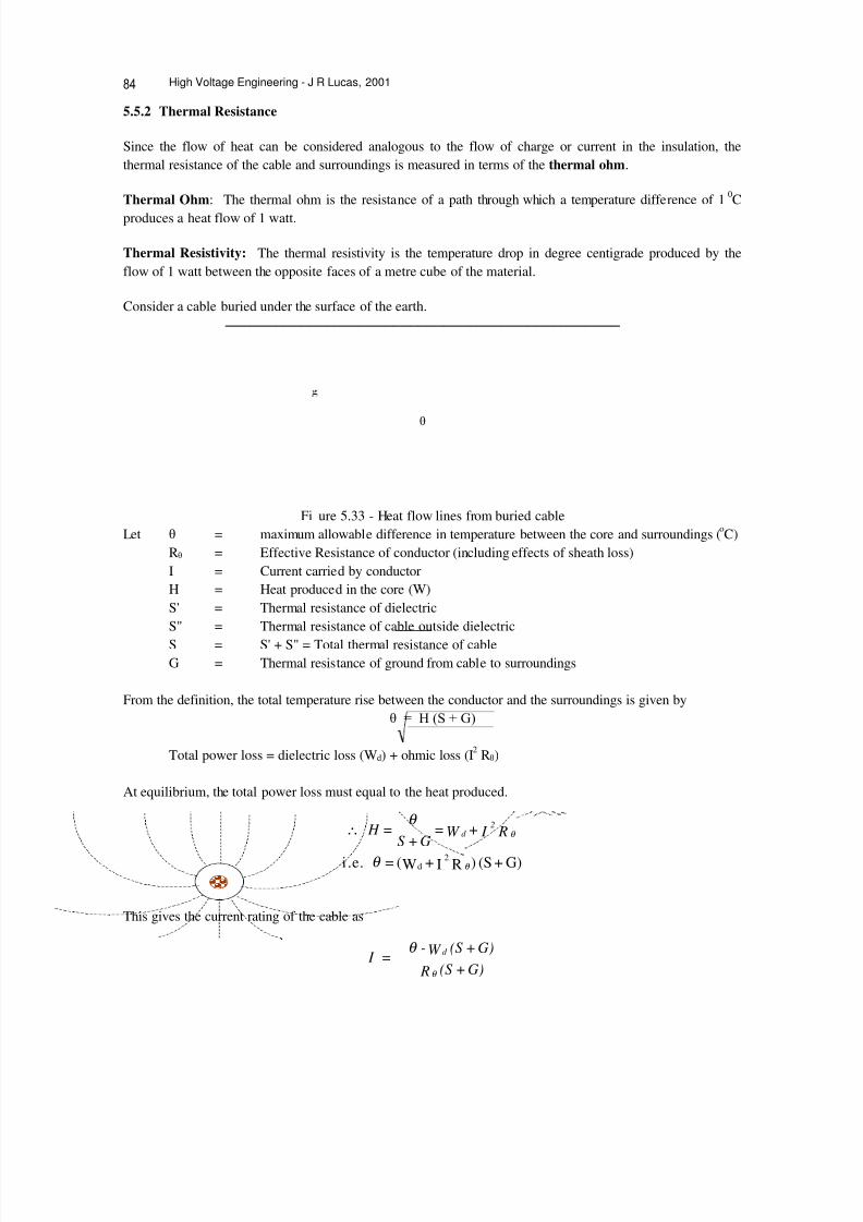
8/6/2019 High Voltage Engineering (Lucas)
http://slidepdf.com/reader/full/high-voltage-engineering-lucas 92/212

8/6/2019 High Voltage Engineering (Lucas)
http://slidepdf.com/reader/full/high-voltage-engineering-lucas 93/212
High Voltage Cables
In calculating the flow if heat it is useful to to remember the following analogies.
Heat Electricity Electrostatic Electromagnetic
Temperature Difference
Potentialdifference
Potential difference magnetomotive force(mmf)
Heat Flow H Current I Electric charge Q Magnetic flux 3
Thermal resistance S Resistance 1/Capacitance Reluctance
If a method exists to study any of the above phenomena, the analogous quantity can also be studied bycomparison.
5.5.3 Thermal Resistance of single-core cable
The analysis of this problem is similar to the analysis of the analogous electrostatic case. Figure 5.34 showsthese two cases.
In the heat problem, H is the amount of heat generated per unit length of cable, and in the correspondingelectrostatic case, q is the electric flux flowing out per unit length.
For the electrostatic case, consider a gaussian cylinder of radius x and thickness dx .
D . 2 [ O T VR WKDW ' T[
Considering the analogous heat flow case,
Let d drop in temperature across dxk = thermal resistivity
equi-temperaturelines
equi-potentiallines
lines of lines of heat flow charge flow
Figure 5.34 - Analogous heat-flow and charge-flow lines
rr log
2q
=xd.x1
. 2
q =V
=where
2
1e
r
r
r0
1
2ε π ε π
ε ε ε π ε
ξ
∫ ∴
∴ , x2
q =
r1
r2
x dx
H r1
r2
x dx
q

8/6/2019 High Voltage Engineering (Lucas)
http://slidepdf.com/reader/full/high-voltage-engineering-lucas 94/212
High Voltage Engineering - J R Lucas, 2001
Thermal resistance is + VR WKDW
5.5.4 Thermal resistance of three-core cables
For three-core cables, the following two quip expressions are used.
5.5.5 Thermal resistance of protective coverings
Since the protective covering of the cable is in the form of a cylinder, the expression is of the same form asthat for a single core cable.
wherer3 = radius of outer covering of cabler2 = radius of lead sheathA = thickness of armouringk = thermal resistivity
5.5.6 Thermal resistance of ground around cable
Inside the cable constant temperature lines would all be concentric cylinders since the outer lead sheath is aconductor of heat. The flow of heat would consequently be radial.
However, outside the cable, the equi-temperature lines would no longer be concentric and the heat flow wouldgo radially outwards from the surface of the cable and ending up at the surface of the ground normally(assuming that the surface of the earth is at a constant temperature).
rrlog
2Hk
= givesnintegratio
x2dx.H.k
=d then
2
1eπ
θ
π θ
rrlog
2k
=S resistancethermal2
1eπ
∴
dielectricof radiusouter=r
liesconductoreachof centresheat which tradius=a
conductorof radius=r
where
rar3a-rln
6k
=S (ii)
conductorof radius=r
insulationconductorof thickness=T
insulationbeltof thickness=t
where
kmln
2
22
3
62
6
Ω
π
π / 1+
r
t +T
T
t 1.1 +4.15
T
t 0.2 +0.85
6
k =S(i)
A/2+r
A/2-r 2k
=S2
3lnπ

8/6/2019 High Voltage Engineering (Lucas)
http://slidepdf.com/reader/full/high-voltage-engineering-lucas 95/212
High Voltage Cables
Here again, let us analyse using the analogy of the infinitely long conductor carrying a charge q per unit length,placed at a distance h above the earth surface (Figure 5.35).
This has the same effect as having a charge of -q at the same distance beneath the earth.
The effect of the earth can be replaced by an equal and opposite charge on the opposite side of the surface atthe same distance from the surface.
The effects of the charge +q and -q can now be separately considered, and the results superimposed. Eachcharge considered separately will give rise to radial flux lines.
The potential difference between the charges caused by one of the charges is given by
The total potential difference caused between the charges is twice that of the individual charge. This is equalto
Thus the potential difference to the neutral of each conductor is given as
Analogy : The temperature difference from the heat source to earth is given by
Figure 5.35 - Effect of Earth Surface
r h2
2
q =V elog
ε π
r h2
2
q2 =
r h2
2
q)(--q =V ee loglog
ε π ε π
r h2
2
q =V elog
ε π
r h2
2 H k
= elogπ
θ
-
−
h
earth
char e flow
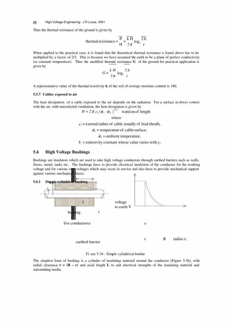
8/6/2019 High Voltage Engineering (Lucas)
http://slidepdf.com/reader/full/high-voltage-engineering-lucas 96/212
High Voltage Engineering - J R Lucas, 2001
Thus the thermal resistance of the ground is given by
When applied to the practical case, it is found that the theoretical thermal resistance a found above has to bemultiplied by a factor of 2/3. This is because we have assumed the earth to be a plane of perfect conductivity(or constant temperature). Thus the modified thermal resistance G of the ground for practical application isgiven by
A representative value of the thermal resistivity k of the soil of average moisture content is 180.
5.5.7 Cables exposed to air
The heat dissipation of a cable exposed to the air depends on the radiation. For a surface in direct contactwith the air, with unrestricted ventilation, the heat dissipation is given by
5.6 High Voltage Bushings
Bushings are insulators which are used to take high voltage conductors through earthed barriers such as walls,floors, metal, tanks etc. The bushings have to provide electrical insulation of the conductor for the workingvoltage and for various over-voltages which may occur in service and also have to provide mechanical supportagainst various mechanical forces.
5.6.1 Simple cylindrical bushing
The simplest form of bushing is a cylinder of insulating material around the conductor (Figure 5.36), withradial clearance t = (R - r) and axial length L to suit electrical strengths of the insulating material andsurrounding media.
rh2
log 2Hk
=H
=resistancethermal eπ θ
r h2
3 H k
=G elogπ
rwithvariesvaluehoseconstant wemissivity=k
,mperatureambient te=
,surfacecableof etemperatur=
,sheathleadof usuallycable,of radiusexernal=r
where
lengthof watt/cm
2
a
s
2
θ θ
θ θ π )-(r 2= H 1.25as2
Fi ure 5.36 - Simple cylindrical bushin
bushing
live conductors
L
t
earthed barrier
voltageto earth V
r R radius x

8/6/2019 High Voltage Engineering (Lucas)
http://slidepdf.com/reader/full/high-voltage-engineering-lucas 97/212

8/6/2019 High Voltage Engineering (Lucas)
http://slidepdf.com/reader/full/high-voltage-engineering-lucas 98/212

8/6/2019 High Voltage Engineering (Lucas)
http://slidepdf.com/reader/full/high-voltage-engineering-lucas 99/212
6
Measurement of High Voltage
6.0 High Voltage Measurement
High voltages can be measured in a variety of ways. Direct measurement of high voltages is possible up to about200 kV, and several forms of voltmeters have been devised which can be connected directly across the test
circuit. High Voltages are also measured by stepping down the voltage by using transformers and potentialdividers. The sparkover of sphere gaps and other gaps are also used, especially in the calibration of meters inhigh voltage measurements. Transient voltages may be recorded through potential dividers and oscilloscopes.Lightning surges may be recorded using the Klydonograph.
6.1 Direct Measurement of High Voltages
6.1.1 Electrostatic Voltmeters
One of the direct methods of measuring high voltages is by means of electro-static voltmeters. For voltagesabove 10 kV, generally the attracted disc type of electrostatic voltmeter is used.When two parallel conducting plates (cross section area A and spacing x) are charged q and have a potentialdifference V, then the energy stored in the is given by
It is thus seen that the force of attraction is proportional to the square of the potential difference applied, so thatthe meter reads the square value (or can be marked to read the rms value).
Electrostatic voltmeters of the attracted disc type may be connected across the high voltage circuit directly to
measure up to about 200 kV, without the use of any potential divider or other reduction method. [The force inthese electrostatic instruments can be used to measure both a.c. and d.c. voltages].
N xV A-=F
xA-=
xdCd thatso
xA=C eCapacitanc fielduniformfor
N xdCd
V=FForce
xdF=CdV=Wdchange thatso VC = WstoredEnergy
2
2
21
2
221
2212
21
ε
ε ε
∴
∴

8/6/2019 High Voltage Engineering (Lucas)
http://slidepdf.com/reader/full/high-voltage-engineering-lucas 100/212
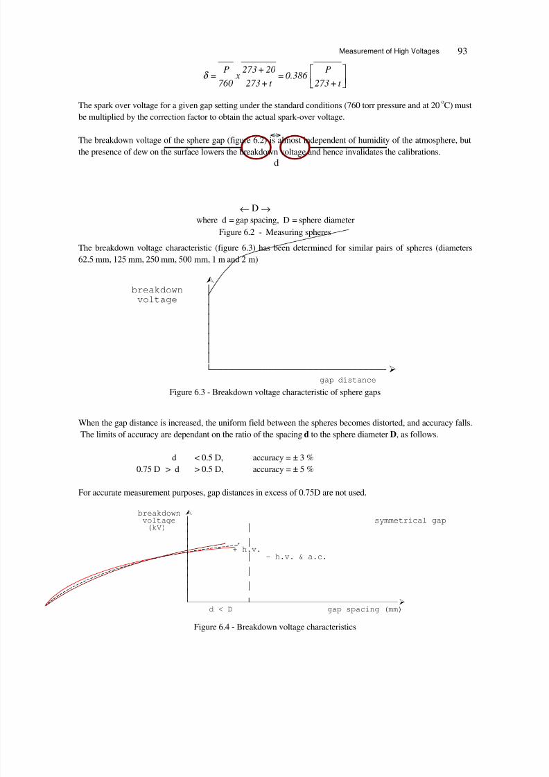
8/6/2019 High Voltage Engineering (Lucas)
http://slidepdf.com/reader/full/high-voltage-engineering-lucas 101/212
Measurement of High Voltages 93
The spark over voltage for a given gap setting under the standard conditions (760 torr pressure and at 20 oC) must
be multiplied by the correction factor to obtain the actual spark-over voltage.
The breakdown voltage of the sphere gap (figure 6.2) is almost independent of humidity of the atmosphere, butthe presence of dew on the surface lowers the breakdown voltage and hence invalidates the calibrations.
The breakdown voltage characteristic (figure 6.3) has been determined for similar pairs of spheres (diameters62.5 mm, 125 mm, 250 mm, 500 mm, 1 m and 2 m)
When the gap distance is increased, the uniform field between the spheres becomes distorted, and accuracy falls.The limits of accuracy are dependant on the ratio of the spacing d to the sphere diameter D, as follows.
d < 0.5 D, accuracy = ± 3 %0.75 D > d > 0.5 D, accuracy = ± 5 %
For accurate measurement purposes, gap distances in excess of 0.75D are not used.
t +273P
0.386 =t +273
20+273 x
760P
=δ
d
←D → where d = gap spacing, D = sphere diameter
Figure 6.2 - Measuring spheres
¿ breakdown G
voltage G G G G G G
G JFFFFFFFFFFFFFFFFFFFFFFFFFFFFFFF¾ gap distance
Figure 6.3 - Breakdown voltage characteristic of sphere gaps
breakdown ¿ voltage G V\PPHWULFDO JDS
(kV) G G G G G G h.v.G G - h.v. & a.c.G G G G G G G
JFFFFFFFFFFFFOFFFFFFFFFFFFFFFFFFFFFFFFFFFFFFF¾ d < D gap spacing (mm)
Figure 6.4 - Breakdown voltage characteristics
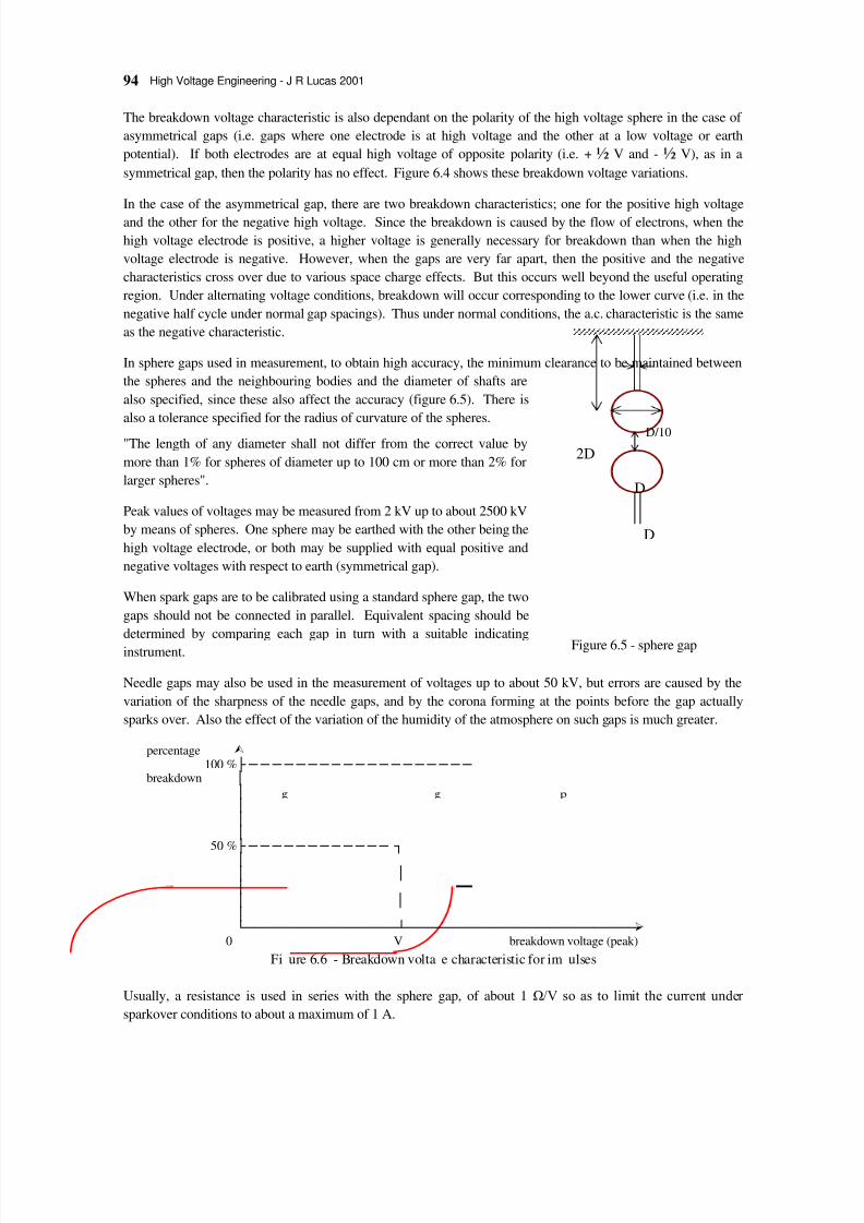
8/6/2019 High Voltage Engineering (Lucas)
http://slidepdf.com/reader/full/high-voltage-engineering-lucas 102/212
94 High Voltage Engineering - J R Lucas 2001
The breakdown voltage characteristic is also dependant on the polarity of the high voltage sphere in the case of asymmetrical gaps (i.e. gaps where one electrode is at high voltage and the other at a low voltage or earthpotential). If both electrodes are at equal high voltage of opposite polarity (i.e. + ½ V and - ½ V), as in asymmetrical gap, then the polarity has no effect. Figure 6.4 shows these breakdown voltage variations.
In the case of the asymmetrical gap, there are two breakdown characteristics; one for the positive high voltageand the other for the negative high voltage. Since the breakdown is caused by the flow of electrons, when thehigh voltage electrode is positive, a higher voltage is generally necessary for breakdown than when the highvoltage electrode is negative. However, when the gaps are very far apart, then the positive and the negativecharacteristics cross over due to various space charge effects. But this occurs well beyond the useful operatingregion. Under alternating voltage conditions, breakdown will occur corresponding to the lower curve (i.e. in thenegative half cycle under normal gap spacings). Thus under normal conditions, the a.c. characteristic is the sameas the negative characteristic.
In sphere gaps used in measurement, to obtain high accuracy, the minimum clearance to be maintained betweenthe spheres and the neighbouring bodies and the diameter of shafts arealso specified, since these also affect the accuracy (figure 6.5). There isalso a tolerance specified for the radius of curvature of the spheres.
"The length of any diameter shall not differ from the correct value bymore than 1% for spheres of diameter up to 100 cm or more than 2% forlarger spheres".
Peak values of voltages may be measured from 2 kV up to about 2500 kVby means of spheres. One sphere may be earthed with the other being thehigh voltage electrode, or both may be supplied with equal positive and
negative voltages with respect to earth (symmetrical gap).
When spark gaps are to be calibrated using a standard sphere gap, the twogaps should not be connected in parallel. Equivalent spacing should bedetermined by comparing each gap in turn with a suitable indicatinginstrument.
Needle gaps may also be used in the measurement of voltages up to about 50 kV, but errors are caused by thevariation of the sharpness of the needle gaps, and by the corona forming at the points before the gap actuallysparks over. Also the effect of the variation of the humidity of the atmosphere on such gaps is much greater.
Usually, a resistance is used in series with the sphere gap, of about 1 9 VR DV WR OLPLW WKH FXUUHQWsparkover conditions to about a maximum of 1 A.
Figure 6.5 - sphere gap
percentage¿
100 % L F F F F F F F F F F F F F F F F F F F breakdown G
G G G G
50 % L F F F F F F F F F F F F I G G G G G G G JFFFFFFFFFFFFFFFFFOFFFFFFFFFFFFFFFFFFFFFFFFFF ¾
0 V breakdown voltage (peak)Fi ure 6.6 - Breakdown volta e characteristic for im ulses
D
D
2D
D/10

8/6/2019 High Voltage Engineering (Lucas)
http://slidepdf.com/reader/full/high-voltage-engineering-lucas 103/212
Measurement of High Voltages 95
However for impulse measurements, a series resistance must not be used since this causes a large drop across theresistance. In measuring impulse voltages, since the breakdown does not occur at exactly the same value of voltage each time, what is generally specified is the 50 % breakdown value. A number of impulses of the samevalue is applied and a record is kept of the number of times breakdown occurs, and a histogram is plotted with
the peak value of the impulse voltage and the percentage of breakdown (figure 6.6).
6.2 Transformer and potential divider methods of measurement
6.2.1 Transformer ratio method
The use of the primary voltage to estimate the secondary voltage is a fairly rough method of measurement, but issatisfactory enough for most ac tests. In this method (figure 6.7), the voltage on the low voltage side of thehigh-tension transformer is measured. The actual voltage across the load is not measured.
Since the current taken by the device under test is usually very small, currents such as due to corona may causeconsiderable error in the measured voltage. This method measures the rms voltage. In order to determine thepeak value it is necessary to determine the wave form of the secondary voltage.
Some high voltage transformers (figure 6.8) carry a separate voltmeter-coil having a number of turns which is a
definite fraction of the secondary turns. This method cannot be used with the cascade arrangement of thetransformers.
FFFFFFFFFFFFFFFFFFFFFFFFFI G HOI FXUUHQW
G G OLPLWLQJ G G UHVLVWDQFH JNK 9
HFFFFFFFFFFNFFFFFFFF G G G
a.c. G V HOI
supply G G 7HVW G G G GHYLFH
JFFFFFFFFFFOFFFFFFFF JNK G
FFFFFFFFFFFFFFFFFFFFFFFFFM FOF (
F
Figure 6.7 - transformer ratio method
FFFFFFFFFFFFFFFFFFFFFFFFFI HOI FXUUHQW G G OLPLWLQJ G G UHVLVWDQFH JNK 9
HFFFFFFFFFFFFFFFFFFF G G
a.c. FFI HOI supply G G G 7HVW G G G GHYLFH
JFFFFFFFFFFFFFFFFFFF G JNK FFFFFFFFFFFFFFFFFFFFFFFFFM
G FOF ( F
V
FOF ( F
Figure 6.8 - with additional potential winding

8/6/2019 High Voltage Engineering (Lucas)
http://slidepdf.com/reader/full/high-voltage-engineering-lucas 104/212
96 High Voltage Engineering - J R Lucas 2001
It may also be possible to have a potential transformer connected across the test device and the voltagemeasured, however this is an expensive arrangement.
Even this method may not be very satisfactory under very high voltage conditions and the series resistancemethod of measurement may be used.
Series resistance method of measurement
In the series resistance method a high series resistance(specially designed to withstand high voltage) and resistanceof 20 k 9 LV XVHG ZLWK PLFUR-DPPHWHU KDYLQJ D$movement). This method is applicable for both ac and dc.A number of resistances would be necessary in series, and toprevent leakage current, we would have to have the wholesystem in a insulated container, which is earthed forshielding purposes. As a safety measure, a safety gap orneon lamp is connected across the micro-ammeter. If weuse a stable supply (of accuracy 0.10%) we would finallyend up with an accuracy of 1%.
When the above method is used for alternating voltages, there would be the effect of the distributed capacitancesas well. The capacitive effects can be reduced by providing a suitable screen, or by balancing the capacitance.
6.2.2 Resistive potential divider method
In this method, a high resistance potential divider is connected across the high-voltage winding, and a definitefraction of the total voltage is measured by means of a low voltage voltmeter.
FFFFFFFFFFFFFFFFFFFFFFFNFFFFFFFFFFFFFFFFFFFFF G
HOI FXUUHQW G G OLPLWLQJ G G UHVLVWDQFH JNK 9
HFFFFFFFFF G
G a.c. G FFFFFFI
HOI G supply G G 7HVW UDQJH
G G GHYLFH V 0-110 VJFFFFFFFFF JNK
G G FFFFFFFFFFFFFFFFFFFFFFFPFFFFFFFFFFFFFFFFFFFFF FFFFFFK
high voltage FOF ( 3RWHQWLDO transformer F WUDQVIRUPHU
Fi ure 6.9 - with otential transformer
h.v. FFFFFFFFFFFFFFI G
HOI KLJK VHULHV G G UHVLVWDQFH G G JNK N 9
G HFFFFFFFFM G G
$ G PRYHPHQW $ À
safety gapG ¿ JFFFFFFFFM
FOF F
Fi ure 6.10 - Series resistor microammeter
FFFFFFFFFFFFFNFFFFFFFFFFFFFFFFFFFFI G G
HOI HOI G G FXUUHQW G G G G OLPLWLQJ G G UHVLVWLYH JNK UHVLVWDQFH G G GLYLGHU
HFFFFFFFFFFFF G G G ≈ N 9 G JNK
a.c. G LFFFFFFFFFFFFI HOI G G
supply G G 7HVW HOI G G GHYLFH G G 9
JFFFFFFFFFFFF JNK G G G JNK G
FFFFFFFFFFFFFM G G h.v.
FOF FOF ( FOF
transformer F F F
Fi ure 6.11 - Resistive potential divider method

8/6/2019 High Voltage Engineering (Lucas)
http://slidepdf.com/reader/full/high-voltage-engineering-lucas 105/212
Measurement of High Voltages 97
Under alternating conditions there would be distributed capacitances. One method of eliminating this would beto have a distributed screen of many sections and using an auxiliary potential divider to give fixed potential tothe screens.
The currents flowing in the capacitances would be opposite in directions at each half of the screen so that therewould be no net capacitive current (Figure 6.12 (a)).
It also possible to have a metal conical screen (Figure 6.12 (b)). The design has to be done by trial and error.There would be capacitances to the conical screen as well as capacitances to earth, so that if at any point thecapacitive current from conical screen to the point is equal to that from the point to the earth, then thecapacitances would have no net effect.
6.2.3 Capacitive potential div ider method
For alternating work, instead of using a resistive potential divider, we could use a capacitive potential divider. Inthis two capacitances C 1 and C 2 are used in series, the electrostatic voltmeter being connected across the lowercapacitor.
If the system is kept at a fixed position, we can make corrections for the fixed stray capacitances. Or if screensare used, the capacitance to the screen would be a constant,and we could lump them up with the capacitances of the arms.
Neglecting the capacitance of the voltmeter (or lumping the electrostatic voltmeter capacitance with C 2) theeffective capacitance of C 1 and C 2 in series is C 1C2 /(C 1+C 2), and since the charge is the same,
(a) (b)
Fi ure 6.12 - Screenin of resistive dividers
FFFFFFFFFFFFNFFFFFFFFFFFFFFFFFFI G G
HOI G limiting G G VWUD\ G +LJK 9ROWDJH
G G & FFOFF resistance G G FFNFF &DSDFLWRU
HFFFFFFFFFFFF JNK G G LFFFFFFFFFFFFI
a.c. HOI G G Test G G G G
supply G G & FFOFF HOHFWURVWDWLF device G G FFNFF 9
JFFFFFFFFFFFF JNK G YROWPHWHU G G G
FFFFFFFFFFFFM G G FOF FOF ( FOF
h.v. transformer F F F
Fi ure 6.13 - Capacitive potential divider method

8/6/2019 High Voltage Engineering (Lucas)
http://slidepdf.com/reader/full/high-voltage-engineering-lucas 106/212
98 High Voltage Engineering - J R Lucas 2001
The capacitance of h.v. standard capacitor must be accurately known, and the capacitance must be free from
dielectric losses.For this reason, air capacitances are always used for this purpose.This method also measures ther.m.s. value.
It is sometimes more useful to have a measure of the peak value of the alternating voltage rather than the r.m.s.value,since it is the peak value of the applied voltage which produces the actual breakdown stress in the materialunder test.
If the shape of the voltage waveform is known, the peak voltage may be obtained from the r.m.s. voltage.It isoften more satisfactory however, to use some method of voltage measurement which gives the peak value of thevoltage directly.
6.2.4 Matching of Potential dividers
When waveforms are observed on the oscilloscope, through a potential divider, a cable is necessary to connectthe test waveform to the oscilloscope, and also to cause a small delay between the arrival of the trigger pulse andthe waveform (Figure 6.14).
If the delay cable is lossless , then it may be represented by purely inductances and capacitors, so that the surge
impedance of cable or delay network = Zo = [z/y]1/2
. In a lossless cable , Zo is purely resistive.Velocity of the wave in cable =
ε ε µ r
8
0
10 x3 =
1
C L
1 ≈
The oscilloscope can display a maximum of about 50 V to 100 V and thus the impulse voltage must be reducedby a suitable potential divider. The requirement of the potential divider used are that it reduces the appliedvoltage without producing any distortion (i.e: the ratio of the potential divider does not vary with time orfrequency). The potential divider can be of two types.
(i) Resistiveand (ii)Capacitive.
In practice , neither case is obtained in the pure form, but a mixture of both.The capacitive effect in the resistivedivider is much more than the resistive effect on the capacitive divider.
V.C+C
C = V.CC / )C+C(
C / 1 = C acrossVoltage
21
1
2121
22
impulse FFFFFFFFFFNFFFFFFFFFFFFFFI G G
waveform G G G HOI SRWHQWLDO G G G G G G GLYLGHU
HOI G G G G JNK 'HOD\ FDEOH
Test G G G FFFFFFFFFFFFFFFFFFFFFFFFFFFFFFFFFFFFF G G LFFFFFFFFFFFFFFFFFFFFFFFFFFFFFFFFFFFFFFFFFFFI
device G G G FFFFFFFFFFFFFFFFFFFFFFFFFFFFFFFFFFFFF G G G G DLU LQVXODWHG G < -platesG G HOI FFOFF JNK G G X-platesG G G G G G JNK VLQJOH VZHHS HFFFFM LFFFFI G G G G G G
FOF FOF HFFFFFFFI G FOF F F G 7LPH G G FFNFF F
FFFF! FFFFFFFFM LFFFFK G Trigger pulse G EDVH G FOFRVFLOORVFRSH
JFFFFFFFK F
Fi ure 6.14 - Observation of impulse waveform throu h potential divider

8/6/2019 High Voltage Engineering (Lucas)
http://slidepdf.com/reader/full/high-voltage-engineering-lucas 107/212
Measurement of High Voltages 99
In the case of the resistive divider , the lower arm of the divider has its resistance fixed by the surge impedanceof the cable used (for matching ) and by the wave-tail requirements of the impulse generator circuit (if anyimpulse generator is used).The ratio of the divider is determined by the sensitivity of the C.R.O and the voltage.
The capacitive divider is generally bulkier than the resistive divider , but has several advantages. It can be used
as part of the wavefront forming circuit. The self capacitance of the cable connecting the device to the C.R.Oadds to the capacitance of the cable connecting the divider to the oscilloscope adds to the capacitance of thelower arm.
When the initial part of the surge enters the cable, it acts as a transmission line and presents its surge impedanceto the surge, but when the line becomes charged, it behaves as a capacitor.
When using potential dividers, it is necessary to suitably terminate the cable at the two ends so as to have perfectmatching of the cables at two ends.
Resistive potential dividers
There are three ways in which they may be matched to delay cables.
(1) Matching at potential divider end only:
In this arrangement, the receiving (ie: the end connected across the CRO Y-plates) is kept on open circuit, andwe try to obtain perfect matching at the sending end, so that there is no reflection, and perfect reflection at the
receiving end.
For perfect matching at the sending end, the equivalent impedance of thesection before the cable must be Z O
Impedance = R 3 + R 1 //R 2 = R 3 + R 1.R2 /(R 1 + R 2)= ZO for perfect matching at s.e
If R1 >> R 2 as usually is, then we have R1//R2 ≈R2 , ∴ ZO = R 2 + R 3
InputE FFF! FFFFI
Impulse 1 G HOI
R G G 1 G G 5 =
JNK ( ( G HFFFFI FFFFFFFFFFFFFFFFFFFFF
E LFFFFM LFFFFFFFFFFFFFFFFFFFFFFFFFFFFFFI < -plates2 G JFFFFK FNFFFFFFFFFFFFFFFFFFF G HOI FOF FDEOH FFFOFFF
R G G F 2 G G G G
JNK G G G HFFFFFM LFFFI
FOF G G G G F FFF! FFFFK G G FOF
trigger F FFFNFFF
G FOF
F
Fi ure 6.15 - Matchin of resistive divider at sendin end onl
HFFFFFFFI G G G HOI G G G 5 G G G G G G 5 G JNK G G HFFFFFI G LFFFM LFFFF G G JFFFFFK G HOI G G G 5 G G G ½ FFF G G G G JNK G G JFFFFFFFOFFFFFFFFFFFFFF
Fi ure 6.16
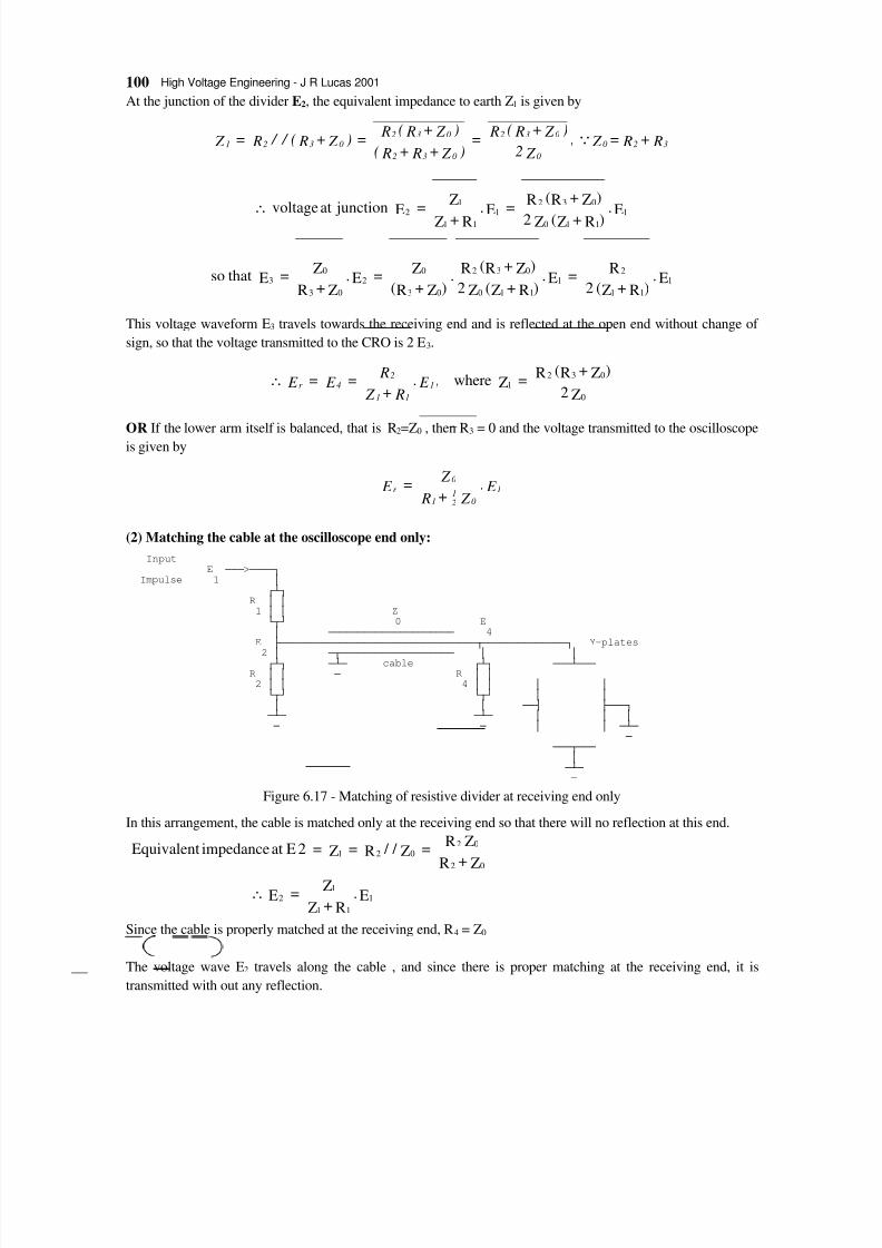
8/6/2019 High Voltage Engineering (Lucas)
http://slidepdf.com/reader/full/high-voltage-engineering-lucas 108/212
100 High Voltage Engineering - J R Lucas 2001
At the junction of the divider E 2, the equivalent impedance to earth Z 1 is given by
This voltage waveform E 3 travels towards the receiving end and is reflected at the open end without change of sign, so that the voltage transmitted to the CRO is 2 E 3.
OR If the lower arm itself is balanced, that is R 2=Z0 , then R 3 = 0 and the voltage transmitted to the oscilloscopeis given by
(2) Matching the cable at the oscilloscope end only:
In this arrangement, the cable is matched only at the receiving end so that there will no reflection at this end.
E.R+Z
Z = E
Z+RZR = Z / / R = Z = 2EatimpedanceEquivalent
111
12
02
02021
∴
Since the cable is properly matched at the receiving end, R 4 = Z 0
The voltage wave E 2 travels along the cable , and since there is proper matching at the receiving end, it istransmitted with out any reflection.
E.)R+Z(2
R = E.)R+Z(Z2)Z+R(R .
)Z+R(Z = E.
Z+RZ = E thatso
E.)R+Z(Z2)Z+R(R = E.
R+ZZ = E junctionatvoltage
111
21
110
032
03
02
03
03
1110
0321
11
12
R+ R= Z , Z 2
) Z + R( R = ) Z + R+ R(
) Z + R( R = ) Z + R( / / R = Z 3200
032
032
0320321
∴
Z2)Z+R(R
= Z where 0
0321 , E . R+ Z
R = E = E 1
11
24r
∴
E . Z + R
Z = E 102
11
0r
InputE FFF! FFFFI
Impulse 1 G HOI
R G G 1 G G =
JNK ( G FFFFFFFFFFFFFFFFFFFFF 4
E LFFFFFFFFFFFFFFFFFFFFFFFFFFFFFFFFFNFFFFFFFFFFFFFFI< -plates2 G FNFFFFFFFFFFFFFFFFFFF G G
HOI FOF FDEOH HOI FFFOFFF R G G F 5 G G
2 G G G G G G JNK JNK G G G G FFM LFFFI
FOF FOF G G G F F G G FOF
F FFFNFFF
G
FOF F
Figure 6.17 - Matching of resistive divider at receiving end only

8/6/2019 High Voltage Engineering (Lucas)
http://slidepdf.com/reader/full/high-voltage-engineering-lucas 109/212
Measurement of High Voltages 101
For given values of R 1, R 2 and E 1 this arrangement gives smaller voltages at the C.R.O than when only the
divider end is matched.
If the point E 2 is not connected to earth through the resistance R 2, (ie. if R 2 = ∞), then we have
For this case the voltage at the oscilloscope is given by
(3) Matching at both ends of the cable :
In this case, the cable is matched at both ends . With this termination there is no reflection at either end. Thisarrangement is used when it is necessary to reduce to a minimum the irregularities produced in the delay cablecircuit.
As before, for perfect matching at receiving end, R 4 = Z 0 and for perfect matching at sending end, R 2 + R 3 = Z0.
E . R R+ Z ) R+ R(
Z R = E . R) Z + R(++ Z R
Z R = E . R+ Z
Z = E = E 121021
021
10202
021
11
124∴
InputE FFF! FFFFI
Impulse 1 G HOI
R G G 1 G G =
JNK 0 EG FFFFFFFFFFFFFFFFFFFFF
E JFFFFFFFFFFFFFFFFFFFFFFFFFFFFFFFFFNFFFFFFFFFFFFFFI< -platesFNFFFFFFFFFFFFFFFFFFF G G FOF FDEOH HOI FFFOFFF F 5 G G
4 G G G G JNK G G G FFM LFFFI
FOF G G G F G G FOF
F FFFNFFF
G FOF
F
Fi ure 6.18 - Matchin of resistive divider at receivin end (with R 2 = ∞)
E . R+ Z
Z = E . R R+ Z ) R+ R(
Z R = E 110
01
21021
02
R4 Lt
2 ∞→
InputE FFF! FFFFI
Impulse 1 G HOI
R G G 1 G G 5 =
JNK ( ( G HFFFFI FFFFFFFFFFFFFFFFFFFFF
E LFFFFM LFF FFFFFFFFFFFFFFFFFFFFFFFFFFNFFFFFFFFFFFFFI< -plates2 G JFFFFK FNFFFFFFFFFFFFFFFFFFF G G HOI FOF FDEOH G FFFOFFF
R G G F G 2 G G HOI G G
JNK 5 G G G G G G G FFFFM LFFFI
FOF G G G G G F JNK G G FOF
G F G FFFNFFF G G
FOF FOF F F
Fi ure 6.19 - Matchin of resistive divider at both ends
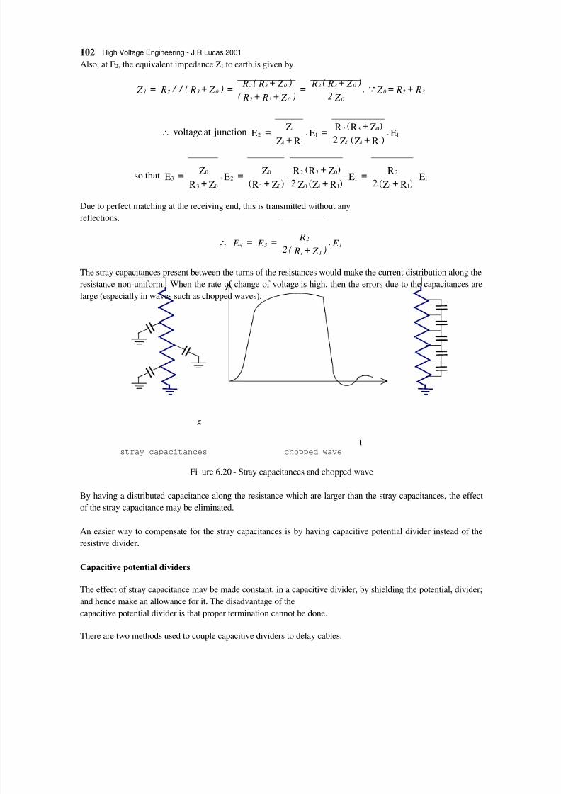
8/6/2019 High Voltage Engineering (Lucas)
http://slidepdf.com/reader/full/high-voltage-engineering-lucas 110/212

8/6/2019 High Voltage Engineering (Lucas)
http://slidepdf.com/reader/full/high-voltage-engineering-lucas 111/212
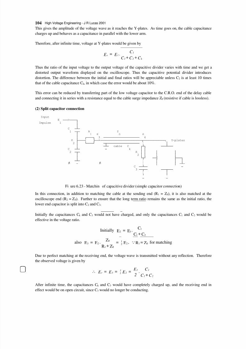
8/6/2019 High Voltage Engineering (Lucas)
http://slidepdf.com/reader/full/high-voltage-engineering-lucas 112/212
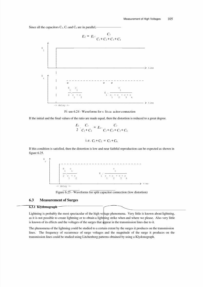
8/6/2019 High Voltage Engineering (Lucas)
http://slidepdf.com/reader/full/high-voltage-engineering-lucas 113/212
Measurement of High Voltages 105
Since all the capacitors C 2, C3 and C k are in parallel,
If the initial and the final values of the ratio are made equal, then the distortion is reduced to a great degree.
If this condition is satisfied, then the distortion is low and near faithful reproduction can be expected as shown infigure 6.25.
6.3 Measurement of Surges
6.3.1 Klydonograph
Lightning is probably the most spectacular of the high voltage phenomena. Very little is known about lightning,as it is not possible to create lightning or to obtain a lightning strike when and where we please. Also very littleis known of its effects and the voltages of the surges that appear in the transmission lines due to it.
The phenomena of the lightning could be studied to a certain extent by the surges it produces on the transmissionlines. The frequency of occurrence of surge voltages and the magnitude of the surge it produces on thetransmission lines could be studied using Litchenberg patterns obtained by using a Klydonograph.
¿ G
E G HFFFFFFFFFFFFFFFFFFFFFFFFFFFFFFFFFFFFFFFFFFFFFFFFFFFFFFFFFFFFFFF 1 G G
G G G G G G G G G G G G JFFFFFOFFFFFFFFFFFFFFFFFFFFFFFFFFFFFFFFFFFFFFFFFFFFFFFFFFFFFFFFFFFFFFF¾ time
G E ¿
r G G G F F F F F F F F F F F F F F F F F F F F F F F F F F F F G G
G G ( F F G G FF FFFFFFF ( FFFFFFFFFFFFFFFF G G F F F F F F G N G JFFFFFOFFFFFFFFFFFFFFFFFFFFFFFFFFFFFFFFFFFFFFFFFFFFFFFFFFFFFFFFFFFFFFF¾ time
-> delay <-
Fi ure 6.24 - Waveforms for s lit ca acitor connection
C +C +C +C C . E = E
k 321
112
C+C = C+C .e.i k 321
C +C +C +C
C . E = C +C
C .2
E
k 321
11
21
11
E ¿ r G
G H F F F F F F F F F F F F F F F F F F F F F F F F F F F F F G G G G ( F cG G G G FF FFFFFFF ( FFFFFFFFFFFFFFFF
G GF F F F + c + c
G G N G G JFFFFFFOFFFFFFFFFFFFFFFFFFFFFFFFFFFFFFFFFFFFFFFFFFFFFFFFFFFFFFFFF¾ time
-> delay <-
Figure 6.25 - Waveforms for split capacitor connection (low distortion)

8/6/2019 High Voltage Engineering (Lucas)
http://slidepdf.com/reader/full/high-voltage-engineering-lucas 114/212

8/6/2019 High Voltage Engineering (Lucas)
http://slidepdf.com/reader/full/high-voltage-engineering-lucas 115/212

8/6/2019 High Voltage Engineering (Lucas)
http://slidepdf.com/reader/full/high-voltage-engineering-lucas 116/212

8/6/2019 High Voltage Engineering (Lucas)
http://slidepdf.com/reader/full/high-voltage-engineering-lucas 117/212
Measurement of High Voltages 10
For the circuit shown in figure 6.32, and the corresponding waveforms in figure 6.33 (a),
Since a d.c meter is used it would read I av, and hence would correspond to the maximum value of voltage,independent of the waveform, except in the case when there is more than one maxima and minima per cycle. Insuch a case the meter reading would no longer corresponds to the actual maxima (Figure 6.33(b)), but anaddition of successive peak-to-peaks.
Instead of using a half wave rectifying unit as infigure 6.32, we could also used a full wave rectifyingunit as shown in figure 6.34.
In this case, the reading of the meter wouldeffectively be double giving the result
Thus using either half wave or full wave rectifyingunits, we can obtain the peak value of the voltageindependent of the wave form, if the capacitance andfrequency are known from the reading of the d.cmeter.
(a) Sinusoidal Waveform (b) Non-sinusoidal Waveform
Figure 6.33 - Waveforms for peak measurement
f C2I =
C2I.
= V giving ,V2.C = .I
Vd.C =td.i thatso
avavmaxmaxav
B
A
B
A
τ τ ∴
∫ ∫ ,t d vd C = i
Fi ure 6.34 - Full wave circuit
f C 4 I = V
avmax
B
A
BA
i
v
i
v
τ
Vma
t
t
t
t
Supply
d.c.
+ −

8/6/2019 High Voltage Engineering (Lucas)
http://slidepdf.com/reader/full/high-voltage-engineering-lucas 118/212
110 High Voltage Engineering - J R Lucas 2001
6.4.2 Oscilloscope for measurement of fast transients
High voltage oscilloscopes are used for the study of fast transient phenomena, particularly in the work on high-voltage and on spark breakdown in small gaps.These have a high sweep speed. Since the speed is high, theintensity is lowered and hence a higher intensity is required. In these the beam should not come on till the
transient comes in because;(a) if it is stationary, the spot of high intensity would fog the photograph before the transient comes on, and
(b) if it is moving, the beam may have swept before the transient comes.
Thus the beam should be brought on just before the transient comes on, by being triggered by the transient. Thetransient should come on the Y-plate only shortly after the beam, so that the whole transient is clearly seen. Forthis a delay cable is used.
The delay cable ensures that the transient appears slightly after the beam comes on.
Such a scope can have a maximum of 50 V to 100 V applied across Y plate so that we would have to use a
potential divider. For high writing speed,the anode - cathode voltage should be high (50 - 100 kV). The sweepgenerator should produce a single sweep (not repetitive) , as transients are not repetitive, and triggered by thesignal. The delay cable causes the signal to appear at the Y-plates a fraction of a micro second after the sweepgenerator is triggered (100m length of cable may cause a delay of about 0.3 V
6.5 Measurements of capacitance and loss tangent
6.5.1 High Voltage Schering Bridge
The high voltage Schering bridge is the method most widely used for measuring capacitance and loss tangent (or
power factor) in dielectrics. Figure 6.35 shows the arrangement.
One arm of the bridge is the high voltage test capacitor (assumed to be represented by a series combination of capacitance C 1 and resistance P). The other three arms are a standard high voltage capacitor C 2 (generally a lossfree air capacitor of value 100 to 500 pF) a variable low resistance Q, and a parallel combination of a standardlow resistance S and a variable capacitance C 3.
a.c. supply
Figure 6.35 - High Voltage Schering Bridge
P
D
C1
High VoltageCapacitor
High VoltageStandard Capacitor
C2C3
Q
S
SafetyGap100 V
SafetyGa 100 V

8/6/2019 High Voltage Engineering (Lucas)
http://slidepdf.com/reader/full/high-voltage-engineering-lucas 119/212
Measurement of High Voltages 111
The high voltage supply for the bridge is obtained through a high voltage transformer. For reasons of safety,only the high voltage test capacitor and the high voltage standard capacitor will be at high voltage. The othercomponents are at low voltage and are not allowed to have voltages greater than about 100 V applied acrossthem by means of safety gaps connected across them (The safety gaps are either gas discharge gaps or papergaps). The impedance of these arms must thus necessarily be of values much less than that of the high voltagecapacitors. For measurements at power frequencies, the detector used is a vibration galvanometer, usually of themoving magnet type (If the moving coil type is used, it has to be tuned). The arms Q and C 3 are varied to obtainbalance.
It can be shown that this bridge is frequency independent, and that at balance
power factor angle = 3 ORVV DQJOH- 3
≈ WDQ & 3 &1 = & &3 S
The low voltage end of the bridge is usually earthed, and since the voltages across Q and S are limited to about100 V, the detector would also be near earth potential. Thus all the variable arms and the detector can be safelyhandled by the operator.
It should be noted that the bridge is an unequal arm bridge, so that the relative sensitivity will be small.However, since the applied voltage is high, this is not a practical disadvantage and a reasonable variation can beobtained across the detector.
Since the value of the standard capacitor must be accurately known, there should be no distortion of the field init. Thus a high voltage guard is provided in it design. This guard is earthed directly (which causes a smallerror), or kept at the same potential as the main electrode without a direct connection as shown in figure 6.37.
The following procedure is used to have the guard electrode at the same potential as the main electrode. Thebridge is adjusted for balance with the switch in position (a) - the normal Schering Bridge. Then with the switchin position (b) the bridge is again balanced using only S' and C 3'. This ensures that finally a and b are at thesame potential (same potential as the other end of the detector). Successive balance is carried out in positions a and b alternately until final balance is obtained. This connection can be used for capacitances up to 2000 pF.
¿ VG G G G
I G 3 G
G F F F F F F F O F
Figure 6.36
CC =
QP
also2
3 ,SQ
= C C
1
2
Figure 6.37 - Bridge with guarded standard capacitor
P
D
C1
C2C3
Q
S
S′
C3′ a
b
a.c. supply

8/6/2019 High Voltage Engineering (Lucas)
http://slidepdf.com/reader/full/high-voltage-engineering-lucas 120/212

8/6/2019 High Voltage Engineering (Lucas)
http://slidepdf.com/reader/full/high-voltage-engineering-lucas 121/212

8/6/2019 High Voltage Engineering (Lucas)
http://slidepdf.com/reader/full/high-voltage-engineering-lucas 122/212

8/6/2019 High Voltage Engineering (Lucas)
http://slidepdf.com/reader/full/high-voltage-engineering-lucas 123/212
Measurement of High Voltages 115
The apparatus used in the observation (namely the coupling capacitor and the impedance) should be dischargetree, so that all the discharges caused is due to the sample. However, discharges occurring in the transformerand the choke are short circuited through the coupling capacitor and do not affect the measurement. The
discharge pulses caused in the sample are of high frequency, so that we bypass the low frequency and amplifythe high frequency in the measurement circuit.
The coupling capacitor k is provided so that the high frequency components would be provided with a lowimpedance path. In the absence of this low impedance path, the path is highly inductive so that these would actas high impedance to the high frequency.
(c) Using oscilloscope with elliptical time base
In many instances, the detector cannot be used close to equipment, and matching units are employed which
permit the use of about 30 m of co-axial lead between detector and the source of discharge. Calibration is doneby injection of a known step voltage into the system. This gives direct calibration of discharge amplitude andtakes into account the response of the amplifier. The discharge detector input circuit is shown in figure 6.43.The output of the amplifier is displayed on a oscilloscope having an elliptical time base. The time base isproduced from a phase shifting R-C network. It is possible to distinguish between several types of dischargesfrom the nature of the output displayed on the oscilloscope.
QQQQQQQQQFKRNH FFFFFF FFFFFFNFFFFFFFFFFFFFFFFI
G G G G G FFFOFFFGLHOHFWULF
loss-free G FFFNFFF VDPSOH coupling FOF G
capacitor FNF N G HFFFFFFFFFI G LFFFFFFFFM LFFM FFFFFF G HOI G KLJK G G
G LPSHGDQFH G=G G SDVV G G FFF & 5 2 G JNK G ILOWHU G G G LFFFFFFFFM LFFM G G JFFFFFFFFFK
FFFFFF FFFFFFFFFFFFFFFFFFFFFOFFFFFFFFFFFFFFFFK K I DPSOLILHU
h.v. transformer
Figure 6.41 - Circuit for discharge detection
h.f. pulses
low amplitude high frequency pulsessuperposed on sine wave (power freq)
Figure 6.42 - Output waveforms
FFFFFNFFFFFFFFFI G G G FOF G FNF &E G G FR -axial cable
Test FFOFF JFNFFFFFFF HFFFFFFFFFFI voltage FFNFF HOI R FFFNFFF FFFMLFFFFNFFFFFM LFFFFF
G &[ G5 G R HOI G G HOI G G
G G G R G5 G G G G5 G G $PSOLILHU G G JNK R JNK G G JNK G G FFNFOFFFFFFFFFFFOFFFFFFF FFFOFFFFK LFFFFFFFFFFFOFFFFFM LFFFFF
FOF PDWFKLQJ XQLW FOF JFFFFFFFFFFK F F
Figure 6.43 - Discharge detector input circuit

8/6/2019 High Voltage Engineering (Lucas)
http://slidepdf.com/reader/full/high-voltage-engineering-lucas 124/212
116 High Voltage Engineering - J R Lucas 2001
Displays on the oscilloscope for some typical discharges are shown in figure 6. together with correspondingwaveforms arising out of external discharges as well as from contact noise.
(a) For a typical oil-impregnated paper capacitor: The discharges are approximately equal in magnitude andnumber in the two half cycles, but have opposite polarity.
(b) For a polythene insulated cable: The discharges show the asymmetry typical of discharges between aconductor and the solid insulation for a polythene insulated cable.
(c) External discharges: Corona produces a very symmetrical display about the negative voltage peak and asthe voltage increases the discharges spread over a larger part of the ellipse but remain symmetrical.
(d) Contact noise: Bad contacts in the system produce many small discharges at the current peaks.
Oscilloscope connections for elliptical time base
The oscilloscope X and Y plates are supplied from a separate source so as to form an ellipse on the screen. Byapplying the output from the high frequency amplifier to the Y-plates, we can obtain the high frequency pulsesuperposed on the ellipse. The height of the pulse can be measured.
(a) Positive peak (b) Positive peakmarker marker
negative peak Calibration negative peak Calibrationmarker pulse marker pulse
(c) Positive peak (d) Positive peakmarker marker
negative peak Calibration negative peak Calibrationmarker pulse marker pulse
Figure 6.44 - Displays for typical discharges
GG FFFFF! FFFFFFMLFFFFFFFFFFFFFFFFFFFFFFFFFFI
from GG G LFFFFFFFFFFFFFFNFFFFFFFFFFFI
h.f.amplifier pulses from G G G G < G G discharge QQhQQ G G
G G X R R HOI G
HFFFFFc `FFFI G G G G R R G G G G G G G G G VXSSO\ IRU G QQeQQ G JNK G G G G HOOLSWLFDO G G G G JFFFFFFFFFOFFFFFFFFFFFFFFM G WLPH EDVH
C.R.O. G G G FFOFF G G FFNFF G G G G G G G JFFFFFFOFFFFFFFFFFFK
Figure 6.45 - Generation of elliptical time base
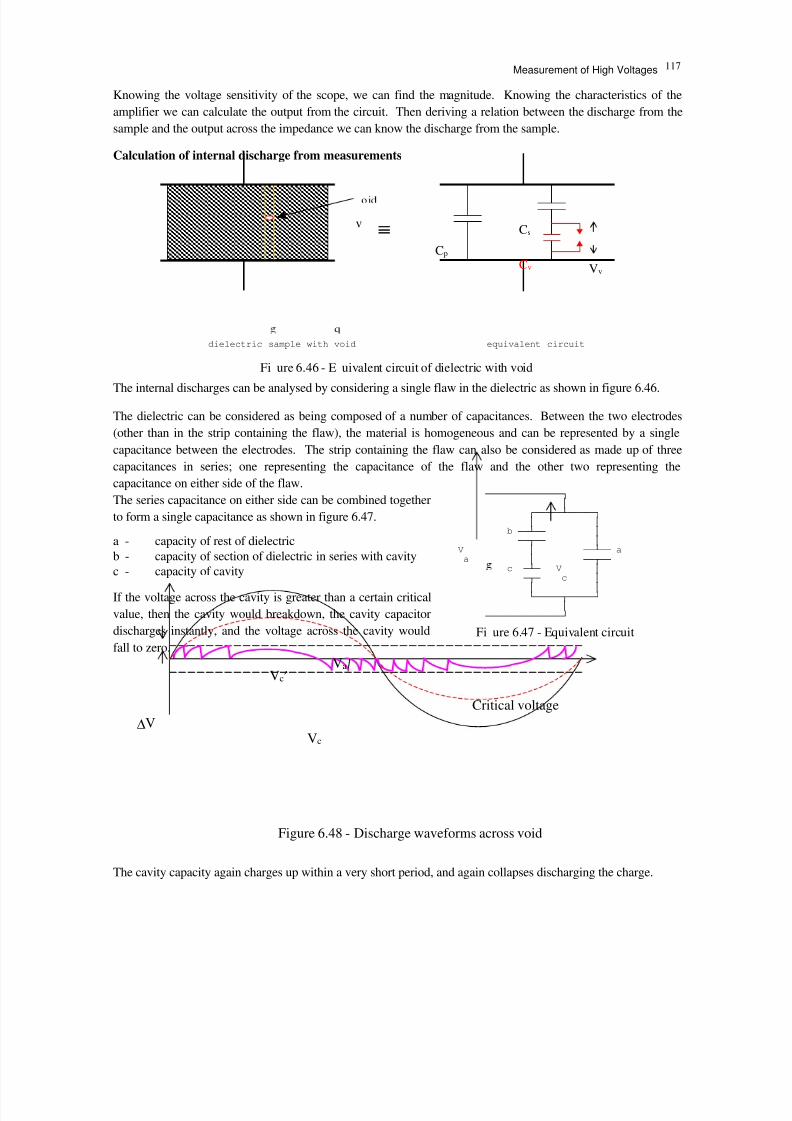
8/6/2019 High Voltage Engineering (Lucas)
http://slidepdf.com/reader/full/high-voltage-engineering-lucas 125/212
Measurement of High Voltages 117
Knowing the voltage sensitivity of the scope, we can find the magnitude. Knowing the characteristics of theamplifier we can calculate the output from the circuit. Then deriving a relation between the discharge from thesample and the output across the impedance we can know the discharge from the sample.
Calculation of internal discharge from measurements
The internal discharges can be analysed by considering a single flaw in the dielectric as shown in figure 6.46.
The dielectric can be considered as being composed of a number of capacitances. Between the two electrodes(other than in the strip containing the flaw), the material is homogeneous and can be represented by a singlecapacitance between the electrodes. The strip containing the flaw can also be considered as made up of threecapacitances in series; one representing the capacitance of the flaw and the other two representing thecapacitance on either side of the flaw.The series capacitance on either side can be combined together
to form a single capacitance as shown in figure 6.47.a - capacity of rest of dielectricb - capacity of section of dielectric in series with cavityc - capacity of cavity
If the voltage across the cavity is greater than a certain criticalvalue, then the cavity would breakdown, the cavity capacitordischarges instantly, and the voltage across the cavity wouldfall to zero.
The cavity capacity again charges up within a very short period, and again collapses discharging the charge.
dielectric sample with void equivalent circuit
Fi ure 6.46 - E uivalent circuit of dielectric with void
FFFFFFFFFFFFFFI G
HFFFFFOFFFFFI G G
b FFOFF G FFNFF G
V G FFOFFD a G FFNFF
c FOF 9 G FNF F G G G JFFFFFNFFFFFK
G FFFFFFFFFFFFFFK
Fi ure 6.47 - Equivalent circuit
Figure 6.48 - Discharge waveforms across void
v
VvCv
Cs
Cp
VaVc′
Critical voltage
Vc ∆V
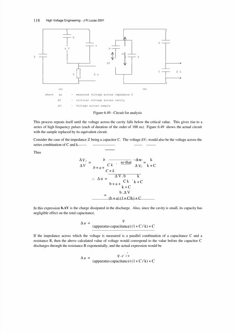
8/6/2019 High Voltage Engineering (Lucas)
http://slidepdf.com/reader/full/high-voltage-engineering-lucas 126/212
118 High Voltage Engineering - J R Lucas 2001
This process repeats itself until the voltage across the cavity falls below the critical value. This gives rise to aseries of high frequency pulses (each of duration of the order of 100 ns). Figure 6.49 shows the actual circuitwith the sample replaced by its equivalent circuit.
Consider the case of the impedance Z being a capacitor C. The voltage û9 1 would also be the voltage across theseries combination of C and k.
Thus
In this expression b. û 9 is the charge dissipated in the discharge. Also, since the cavity is small, its capacity hasnegligible effect on the total capacitance.
If the impedance across which the voltage is measured is a parallel combination of a capacitance C and aresistance R, then the above calculated value of voltage would correspond to the value before the capacitor Cdischarges through the resistance R exponentially, and the actual expression would be
HFFFFFFFFFFFFFFNFFFFFFFFFFFFFI HFFFFFFFFFFFFFFFFFFFFFFFFFI G G G G G G FFOFF G G G G FFNFFE G G G G G G HFFFFOFFFFI FFOFF G G FFOFF G G N FFNFF G FFNFFD FFOFF G G G û 9 G E FFNFF G G
G G G G G FFOFF G G G û9 FFOFF G k FFNFF G G G FFNFFD G
G G G G G G JFFFFFFNFFFFFFK û9 G LFFFFFFFF¾ G LFFFFFFFFFF G G G HOI G G FFOFF G G G G G & FFNFF û X G = G G û X JFFFFNFFFFK G G JNK G LFFFFFFFF¾ G LFFFFFFFFFF G G JFFFFFFFFFFFFFFFFFFFFFK JFFFFFFFFFFFFFFFFFFFFFFFFFK
(a) (b)
where ûX - measured voltage across impedance Z
û9 - critical voltage across cavity
û9 1 - Voltage across sample
Figure 6.49 - Circuit for analysis
C+C/k)+(1a)+(bV.b
=
C+k k
.
C+k k C
+a+b
b.V =u
C+k k
=V
u thatso
1
∆
∆∆∴
∆∆
∆∆
,
k +C k C
+a+b
b =
V V 1
C+k) / C+(1e)capacitanc(apparatusq
=u∆
C+k) / C+(1e)capacitanc(apparatuse.q =u RC
t -
∆

8/6/2019 High Voltage Engineering (Lucas)
http://slidepdf.com/reader/full/high-voltage-engineering-lucas 127/212

8/6/2019 High Voltage Engineering (Lucas)
http://slidepdf.com/reader/full/high-voltage-engineering-lucas 128/212
120 High Voltage Engineering - J R Lucas 2001
If Cv is the value of the variable capacitor at resonance, at the angular frequency & WKHQ
The above calculation is required only if the stray capacitance value is actually required. Otherwise the straycapacitance can be eliminated using the following procedure at the selected frequency (say 1 MHz).
(i) With the outer cell and with only the brass screw and theperspex cover of the inner cell in position, the variablecapacitor C v0 is varied until resonance is obtained. Under thiscondition, only the stray capacitance C 0 is present, and thetotal capacitance will be at resonance with the coil inductanceL. The effective capacitance, in this case, is C v0 + C 0.
The Q-factor of the circuit will be dependant on the resistance r of the coil. The Q-factor can be determinedfrom the half-power points. The variable capacitance is varied in either direction from resonance until the half-
power points (voltage corresponding to 1/ √2) are reached. If C + and C - are the values at the half power points,
then it can be shown that the Q factor is given byIf Q is high,
(ii) The inner electrode is now screwed in, and the circuit is again adjusted for resonance at the same frequency.
If C a is the capacitance of the active portion of thetest cell with air as dielectric, and R a is theequivalent shunt resistance of the circuit with air asdielectric, then the total value of the capacitancerequired must remain the same. This is true for allcases.Thus we have
HFFFFFFFI HFFFFFFFFFFFNFFFFFFM LFFFFFFNFFFFFFFFFFFFFFFFFFFFFNFFFFFFFFFFFFI G G JFFFFFFFK G G G G G 5 G G G G G G G G
G G a.c. V V coil FFOFF& FFOFF WHVW
source FFNFF Y FFNFF FHOO G G G G G
G G G G G G G G G G G G G G G JFFFFFFFFFFFOFFFFFFFFFFFFFFFFFFFFFOFFFFFFFFFFFFFFFFFFFFFOFFFFFFFFFFFFK
Figure 6.53 - Test Circuit
1=)C +C ( L 0v2ω
FFFFFFFFFFFFNFFFFFFFFFFFFFI G G G G G G
r FFOFF& FFOFF& FFNFF Y FFNFF
G G L G G
G G FFFFFFFFFFFOFFFFFFFFFFFFFK
Figure 6.54 - Equivalent circuit for case (i)
pointspowerhalf-at thesvariationtheare C ,C where -+ ∆∆∆∆
∆∆
C +C
)C -C (+C 2 =
C -C C +C =Q
-+
-+
-+
-+
C
C =Q thatso∆
∆∆∆ ,C = C = C -+
FFFFFFFNFFFFFFFFFFFFNFFFFFFFFFFI G G G
r G G LFFFFFFI G G G G G G G HOI
FFOFF& FFOFF& FOF C G G5 FFNFF Y FFNFF FNF D G G D
G G G JNK L G G G G
G G LFFFFFFK G G G
FFFFFFOFFFFFFFFFFFFOFFFFFFFFFFK
Figure 6.55 - Equivalent circuit for case (ii)
C -C = C C +C +C = C +C
vva
a0v0v
10
10
∴

8/6/2019 High Voltage Engineering (Lucas)
http://slidepdf.com/reader/full/high-voltage-engineering-lucas 129/212
Measurement of High Voltages 121
The Q-factor of the circuit however will be different from the earlier value, due to the additional parallelresistance. If the parallel equivalent resistance of the inductor is considered, then it is seen that the overall Qfactor Q a is given as the parallel equivalent of the Q-factors of the coil resistance and the resistance R a. The Q-factor corresponding to the resistance R a is &&5 a, so that
(iii) The liquid is now introduced into the testcell. [The liquid level should be slightly belowthe perspex cover, so that the surface conditionof the perspex is not changed.] If R k is theequivalent shunt resistance of the liquid, and k is the relative permittivity of the liquiddielectric, then the capacitance of the active
portion of the test cell with the liquid would bekCa.If Cv2 is the value of the variable capacitor at resonance, then
Also we have the equivalent Q factor Q k equivalent to the parallel equivalent. Thus
Thus the inverse of &&5 k can be determined from
The loss factor of the dielectric is given by
FFFFFFFNFFFFFFFFFFFFNFFFFFFFFFFFFFFFFFI G G G
r G G LFFFFFFI G G HFFFFFM G G G HOI G HOI
FFOFF& FFOFF& 5 G G FOF & G G5 FFNFF Y FFNFF N G G FNF N G G D
G G JNK G JNK L G G JFFFFFM G
G G LFFFFFFK G G G
FFFFFFOFFFFFFFFFFFFOFFFFFFFFFFFFFFFFFK
Figure 6.56 - Equivalent circuit for case (iii)
RC 1 +
Q1 =
Q1
a La ω
C-CC-C =k
C - C = Ck giving
1v0v
2v0v
2v0va
20
∴
C k + C + C = C + C a0v0v
RC 1
+ RC
1 +
Q1
= Q1
k a Lk ω ω
C)C(
=Q1
,C
)C( =
Q1
usingcalculatedbecan a
a
k
k
∆∆
Q1
,Q1
Q1
- Q1
= RC
1
ak
ak k ω
C-CC-C = factorloss .e.i2v0v
ak ∆∆
[ ]
[ ] C-C.Ck 1
=
CC-C .
Ck C
= Q1
-Q1
.Ck C
=
C
C .
RC1
= RC
1 = factorloss
ak a
ak
aak a
k k k k
∆∆
∆∆
ω ω

8/6/2019 High Voltage Engineering (Lucas)
http://slidepdf.com/reader/full/high-voltage-engineering-lucas 130/212
122 High Voltage Engineering - J R Lucas 2001
Note: in making connections it is essential that care is taken to minimise stray capacitances by using short leads,and the components should not be disturbed during the experiment.
6.5.5 Ionic Wind Voltmeter
When a highly charged point is situated in airor other gas, a movement of the air around thepoint is observed. This is referred to as theelectric wind and is brought about by therepulsion of ions from the surface of the pointby the intense electro-static field. These ionscolliding with uncharged molecules of aircarry them with it setting up the electric wind.A similar wind is observed also at the earthelectrode. In the ionic wind voltmeter, a hot
wire, of platinum-gold alloy, included in onearm of a Wheatstone bridge network is usedas the earthed electrode of high-tension gap.Before the high voltage is applied, the bridgeis balanced. When the voltage of the gapexceeds the "threshold voltage" (voltagerequired before the potential gradient is sufficient for ionization to commence), the electric wind cools the hotwire and hence reduces the resistance. This reduction causes an appreciable out-of-balance voltage in thebridge. The voltage waveform influences the instrument reading, and the instrument is calibrated for a sinewave.
The voltmeter can be used to determine either the peak value or the r.m.s. value of alternating voltages and directvoltages. The principle advantages are that the h.v. may be measured by an observer at some distance from thecharged conductors, and the robust construction and freedom from disturbances by temperature and weatherconditions which make it suitable for outdoor use.
6.5.6 Dumb-bell Voltmeter
A rather specialized way of measuring r.m.s. voltage wasdeveloped by F.M.Bruce in which the period of oscillation of aconducting spheroid in an electro-static field was determined.This enabled the voltage to be determined in terms of length andtime, with an accuracy of 0.05%.
The instrument is shown on figure 6.58.
h.v. line
FFFFFFFFFFFFFFFfFFFFFFFFFFFFFI SQQQQQmQQQQQV G G R G G G VDIHW\ JDS G G G G G G G JFFFFFFFFFFFFFFFFFFFFFI G G G G G G G G G G G G G KRW ZLUH G G G G G HF G G G G * FFFFM G G G G G _QQQQVSQQQQQb G G G G G GJFFFFFOFFFFFFFKG G G G JFFFFFFNFFFFFFNFFK G G G G G G G G G G G
FFFFFFFFFFFFFFFFFFFFFFFF G G E //////////////////////// G G G G G
LFFFFFFFMGGGGLFFFFFFFFFK G G G G
E FOF F
Fi ure 6.57 - Ionic Wind Voltmeter
Figure 6.58 - Dumb-bell voltmeter
ellipsoid
shield

8/6/2019 High Voltage Engineering (Lucas)
http://slidepdf.com/reader/full/high-voltage-engineering-lucas 131/212
7
High Voltage Generatorsfor Testing
7.0 Generation of High Voltages
The power systems engineers is interested in high voltages primarily for power transmission, and secondly fortesting of his equipment used in power transmission. In this chapter we are interested in generating highvoltages for testing of insulation. Thus generation has to be carried out in the testing laboratory. In many testing
laboratories, the primary source of power is at low voltage (400 V three phase or 230 V single phase, at 50 Hz).Thus we need to be able to obtain the high voltage from this. Since insulation is usually being tested, theimpedances involved are extremely high (order of M DQG WKH FXU rents small (less than an ampere). Thereforehigh voltage testing does not usually require high power. Thus special methods may be used which are notapplicable when generating high voltage in high power applications.
7.1 Generation of High Alternating Voltages
Single transformer test units are made for high alternating voltages up to about 200 kV.However, for high voltages to reduce the cost (insulation cost increases rapidly with voltage) and maketransportation easier, a cascade arrangement of several transformers is used.
7.1.1 Cascade arrangement of transformers
Figure 7.1 shows a typical cascade arrangement of transformers used to obtain up to 300 kV from three unitseach rated at 100 kV insulation. The low voltage winding is connected to the primary of the first transformer,and this is connected to the transformer tank which is earthed. One end of the high voltage winding is also
earthed through the tank. The high voltage end and a tapping near this end is taken out at the top of thetransformer through a bushing, and forms the primary of the second transformer. One end of this winding isconnected to the tank of the second transformer to maintain the tank at high voltage. The secondary of thistransformer too has one end connected to the tank and at the other end the next cascaded transformer is fed.This cascade arrangement can be continued further if a still higher voltage is required.
Fi ure 7.1 - Cascade arran ement of transformers
InsulatingPedestal
InsulatingPedestal
1 kV
99 kV
100 kV1 kV
199 kV
200 kV1 kV
200 kV
100 kV
hv output300 kV
bushing
E
99 kV
100 kV
199 kV
200 kV
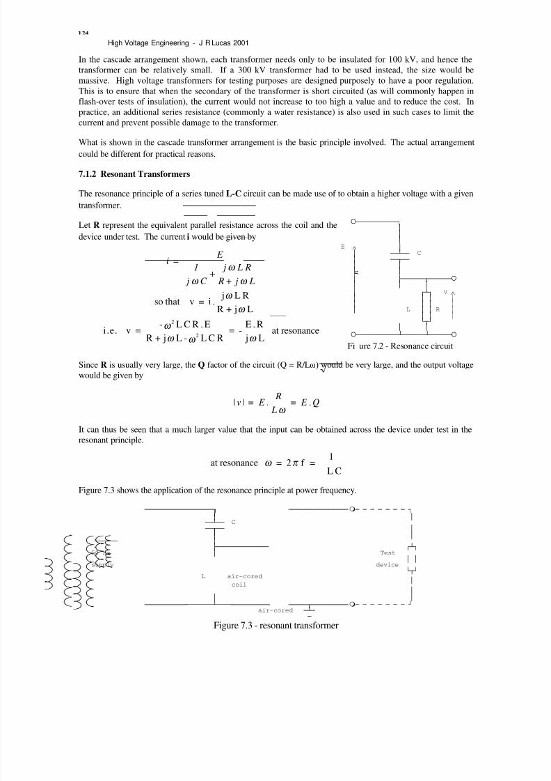
8/6/2019 High Voltage Engineering (Lucas)
http://slidepdf.com/reader/full/high-voltage-engineering-lucas 132/212
High Voltage Engineering - J R Lucas 2001
In the cascade arrangement shown, each transformer needs only to be insulated for 100 kV, and hence thetransformer can be relatively small. If a 300 kV transformer had to be used instead, the size would bemassive. High voltage transformers for testing purposes are designed purposely to have a poor regulation.This is to ensure that when the secondary of the transformer is short circuited (as will commonly happen inflash-over tests of insulation), the current would not increase to too high a value and to reduce the cost. Inpractice, an additional series resistance (commonly a water resistance) is also used in such cases to limit thecurrent and prevent possible damage to the transformer.
What is shown in the cascade transformer arrangement is the basic principle involved. The actual arrangementcould be different for practical reasons.
7.1.2 Resonant Transformers
The resonance principle of a series tuned L-C circuit can be made use of to obtain a higher voltage with a giventransformer.
Let R represent the equivalent parallel resistance across the coil and the
device under test. The current i would be given by
Since R is usually very large, the Q factor of the circuit (Q = R/L & would be very large, and the output voltagewould be given by
It can thus be seen that a much larger value that the input can be obtained across the device under test in theresonant principle.
Figure 7.3 shows the application of the resonance principle at power frequency.
FFFFFFFFFFFI G G
G E ∧ G G FFOFF & G FFNFF G G G G G LFFFFFFNFFFFFF G G G G HOI Y ∧ G G G G G G G G G / G G 5 G
G G G JNK
G G FFFFFFFFFFFOFFFFFFOFFFFFF
Fi ure 7.2 - Resonance circuit
resonanceatL jR.E
- = RCL-L j+R
E.RCL- = v.e.i
L j+R
RL j .i = vthatso
2
2
ω ω ω ω
ω ω
ω ω
ω L j+ R R L j
+C j
1 E
= i
Q. E = L R
. E = |v|ω
CL
1 = f 2 = resonanceat π ω
FFFFFFFFFFFFFFFFFFI FFFFFFFFFFFFFFFF F F F F F F F I G G G FFOFF & FFNFF G G G G
FFFFFF G LFFFFFFFFFFFFFF HOI
50 Hz G 7HVW G G
supply deviceJNK
L air-coredFFFFFF G coil
G G G
FFFFFFFFFFFFFFFFFFOFFFFFFFFFFFFFF FFFFFNFFFFFFFFFF F F F F F F F K air-cored FOF
F
Figure 7.3 - resonant transformer

8/6/2019 High Voltage Engineering (Lucas)
http://slidepdf.com/reader/full/high-voltage-engineering-lucas 133/212

8/6/2019 High Voltage Engineering (Lucas)
http://slidepdf.com/reader/full/high-voltage-engineering-lucas 134/212
High Voltage Engineering - J R Lucas 2001
The supply is usually 50 Hz to the primary of the high voltage testing transformer. [In the circuit shown, C 2 includes the capacitance of the sphere gap used for measurement.] The primary circuit of the tesla transformeralso contains a trigger spark gap. Since the supply to the primary of the tesla transformer is alternating, thecapacitor C 1 is charged up to some maximum voltage, which depends upon the secondary side of the supply
transformer, and upon the setting of the trigger gap.At this voltage, the trigger gap breaks down, the capacitor C 1 discharges, and a train of damped oscillations of high frequency is produced in the circuit containing C 1, the spark gap and the primary winding of the teslatransformer. During the time taken for this train of oscillations to die away, the spark gap is conducting, due tothe formation of an arc across it. This charge and discharge of capacitor C 1 takes place twice in one voltagecycle. Thus there will be a hundred of these trains of damped oscillations per second. The frequency of oscillations themselves is very high (about 100 kHz usually), its actual value depending upon the inductance andcapacitance of the oscillatory circuit.
The circuit parameters are generally such that the resonant frequencies of the two sides are the same.
The expression for the voltage variation being obtained as the solution to a fourth order differential equation.
The solution to the differential equation will generally be in conjugate pairs.
Thus the solution can be written in the form
If the two undamped frequencies are equal (corresponding to L 1C1 = L 1C1), then the damped resonantfrequencies are nearly equal ( & 1 ≈ & 2).
The exponential decays of the components of the voltage depends on the resistance values.
If amplitudes A 1 and A 2 are equal, and the decays also equal, then the summation in v would have the form
If & 1 ≈ & 2, then ( & 1 + & 2)/2 ≈ & VR WKDW WKH VXP RI WKH WZR VLQH WHUPV UHSUHVHQWV D SURwhich is of very nearly the resonant frequency, and the other with a frequency equal to the difference frequencybetween the primary and the secondary resonance frequencies. If the magnitudes and decays were notconsidered equal, the above result will be modified by the constants A 1 and A 2, and the exponential decays e -a1 t and e -a2 t .
The energy tends to get transferred from primary to the secondary and vice versa, so that the voltage of primaryis minimum when the secondary voltage is maximum and vice versa. Oscillation would occur which would bedamped out due to the resistance in the circuit.
ω 22211
1 LC = LC ≈
complexiswhere α α α α α ,e D+eC +e B+e A = v t -t -t -t - 4321
etc.... ; j-a = , j+a = 21 ω α ω α
constantsare ,,,,A,A,a,a where
sinsin
21212121 φ φ ω ω
φ ω φ ω
)+t (e A+)+t (e A = v 22t a-
211t a-
121
2)-+t .-(
.2
)++t .+( 2 = )+t (+)+t ( 21212121
2211φ φ ω ω φ φ ω ω φ ω φ ω cossinsinsin
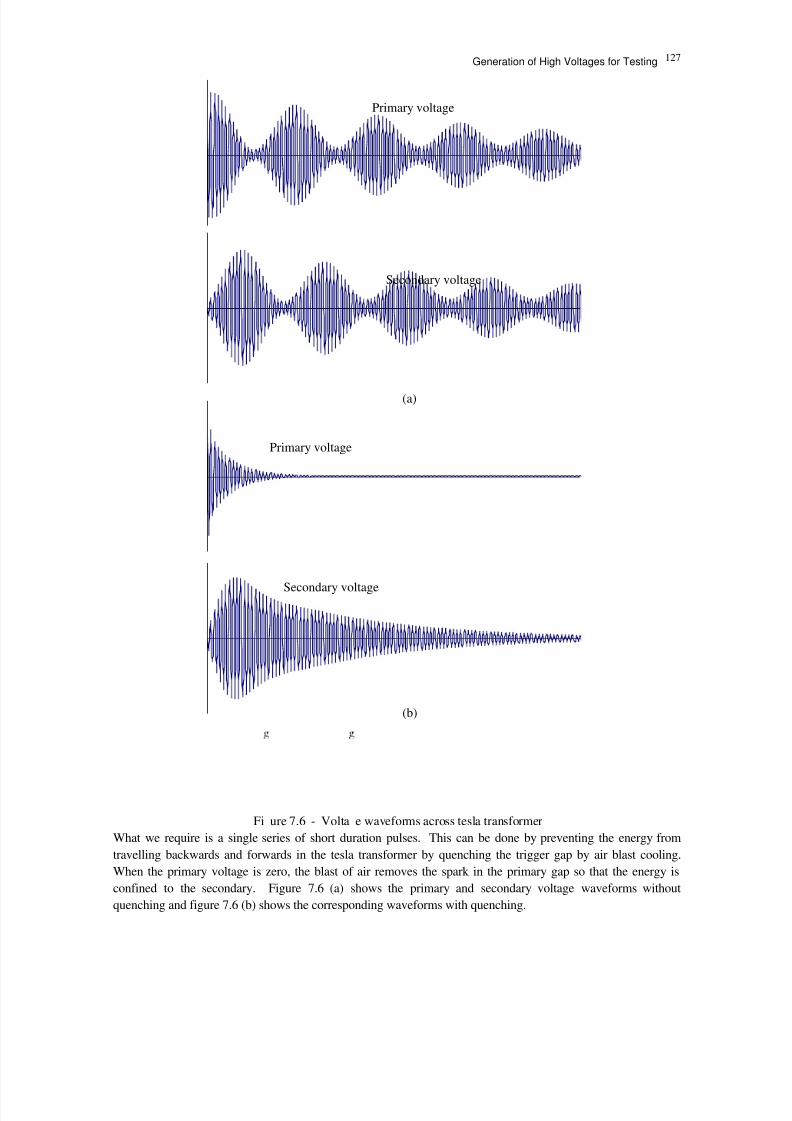
8/6/2019 High Voltage Engineering (Lucas)
http://slidepdf.com/reader/full/high-voltage-engineering-lucas 135/212

8/6/2019 High Voltage Engineering (Lucas)
http://slidepdf.com/reader/full/high-voltage-engineering-lucas 136/212
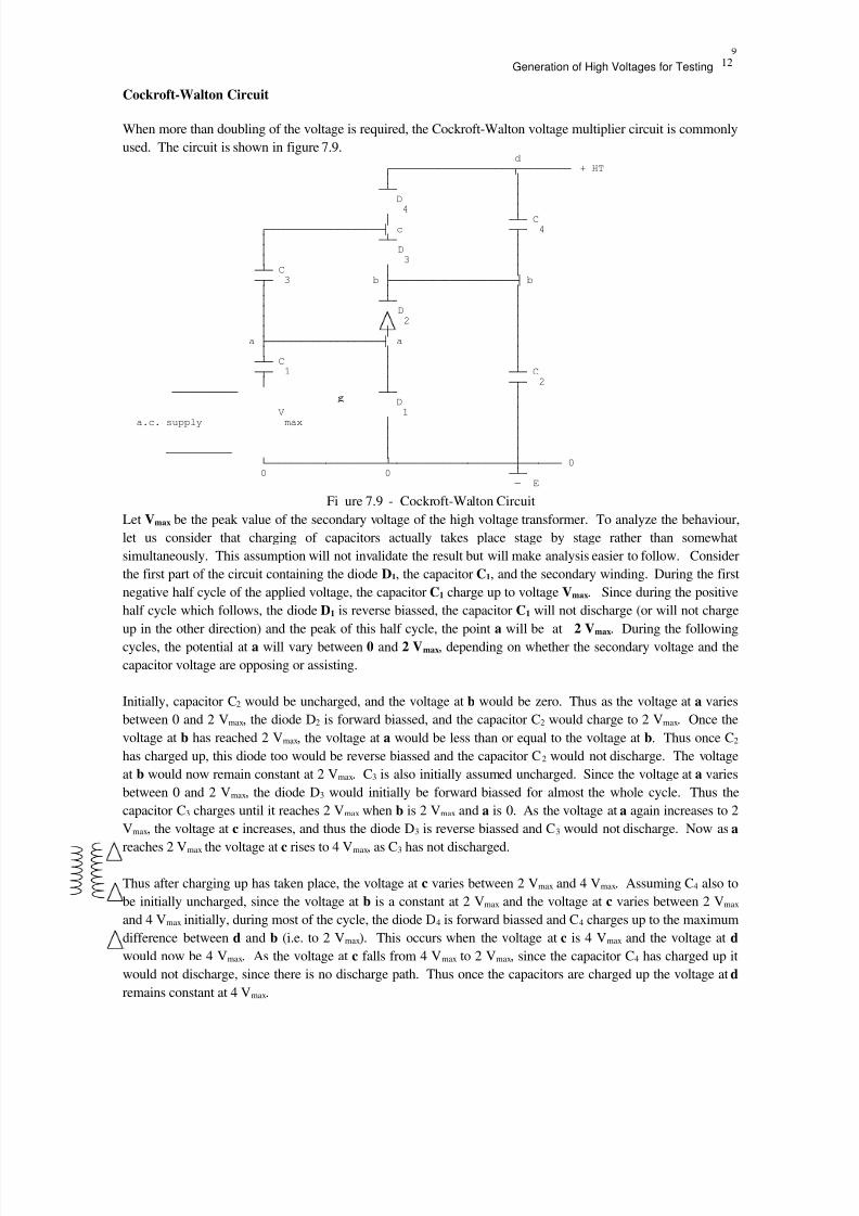
8/6/2019 High Voltage Engineering (Lucas)
http://slidepdf.com/reader/full/high-voltage-engineering-lucas 137/212
Generation of High Voltages for Testing 12
Cockroft-Walton Circuit
When more than doubling of the voltage is required, the Cockroft-Walton voltage multiplier circuit is commonlyused. The circuit is shown in figure 7.9.
Let Vmax be the peak value of the secondary voltage of the high voltage transformer. To analyze the behaviour,let us consider that charging of capacitors actually takes place stage by stage rather than somewhat
simultaneously. This assumption will not invalidate the result but will make analysis easier to follow. Considerthe first part of the circuit containing the diode D1, the capacitor C 1, and the secondary winding. During the firstnegative half cycle of the applied voltage, the capacitor C 1 charge up to voltage Vmax . Since during the positivehalf cycle which follows, the diode D1 is reverse biassed, the capacitor C 1 will not discharge (or will not chargeup in the other direction) and the peak of this half cycle, the point a will be at 2 V max . During the followingcycles, the potential at a will vary between 0 and 2 V max , depending on whether the secondary voltage and thecapacitor voltage are opposing or assisting.
Initially, capacitor C 2 would be uncharged, and the voltage at b would be zero. Thus as the voltage at a variesbetween 0 and 2 V max, the diode D 2 is forward biassed, and the capacitor C 2 would charge to 2 V max. Once thevoltage at b has reached 2 V max, the voltage at a would be less than or equal to the voltage at b. Thus once C 2 has charged up, this diode too would be reverse biassed and the capacitor C 2 would not discharge. The voltageat b would now remain constant at 2 V max. C 3 is also initially assumed uncharged. Since the voltage at a variesbetween 0 and 2 V max, the diode D 3 would initially be forward biassed for almost the whole cycle. Thus thecapacitor C 3 charges until it reaches 2 V max when b is 2 V max and a is 0. As the voltage at a again increases to 2Vmax, the voltage at c increases, and thus the diode D 3 is reverse biassed and C 3 would not discharge. Now as a reaches 2 V max the voltage at c rises to 4 V max, as C 3 has not discharged.
Thus after charging up has taken place, the voltage at c varies between 2 V max and 4 V max. Assuming C 4 also tobe initially uncharged, since the voltage at b is a constant at 2 V max and the voltage at c varies between 2 V max and 4 V max initially, during most of the cycle, the diode D 4 is forward biassed and C 4 charges up to the maximum
difference between d and b (i.e. to 2 V max). This occurs when the voltage at c is 4 V max and the voltage at d would now be 4 V max. As the voltage at c falls from 4 V max to 2 V max, since the capacitor C 4 has charged up itwould not discharge, since there is no discharge path. Thus once the capacitors are charged up the voltage at d remains constant at 4 V max.
dHFFFFFFFFFFFFFFFFFFFFFNFFFFFFFFF +7 G G
FOF G D G
4 G G FOF &
HFFFFFFFFFFFFFFFFFFFFMF FNF G FOF G G ' G G G
FOF & G G FNF b LFFFFFFFFFFFFFFFFFFFFFME
G G G G FOF G G ' G G G G G G
a LFFFFFFFFFFFFFFFFFFFFMD G G G G
FOF & G G
FNF G FOF & G G FNF FFFFFFFFFFF FOF G
D G V 1 G
a.c. supply max G G G G G G
FFFFFFFFFFF G G JFFFFFFFFFFFFFFFFFFFFOFFFFFFFFFFFFFFFFFFFFFPFFFFFFF 0 0 FOF
F (
Fi ure 7.9 - Cockroft-Walton Circuit

8/6/2019 High Voltage Engineering (Lucas)
http://slidepdf.com/reader/full/high-voltage-engineering-lucas 138/212
High Voltage Engineering - J R Lucas 2001
This sequence of voltages gained is shown in Table 7.1.
Cycle
Location
0-
T/2+
T-
3T/2+
2T-
5T/2+
3T-
7T/2+
4T-
a 0 2 Vm 0 2 Vm 0 2 Vm 0 2 Vm 0
b 0 2 Vm 2 Vm 2 Vm 2 Vm 2 Vm 2 Vm 2 Vm 2 Vm
c 0 0 2 Vm 4 Vm 2 Vm 4 Vm 2 Vm 4 Vm 2 Vm
d 0 0 0 4 Vm 4 Vm 4 Vm 4 Vm 4 Vm 4 Vm
Table 1
When the generator is used for a test, or when it is loaded, a current is drawn from the generator, and the
capacitors lose some of their charge to the load, and the voltage falls slightly depending on the load. As thevoltage across any of the capacitors drops, then at some point in the applied alternating voltage cycle, thecorresponding diode would become forward biassed and charging up of the capacitor would once again result.Thus when a load is connected, there would be a small ripple in the output voltage.
7.2.3 Electrostatic generators
Electrostatic generators using the principle of charge transfer can give very high direct voltages. The basicprinciple involved is that the charge is placed on a carrier, either insulating or an isolated conductor, and raisedto the required potential by being mechanically moved through the electrostatic field.
Van de Graeff generator
The Van de Graeff generator is one of the methods used to obtain very high voltages. However they cannotsupply much currents and the power output is restricted to a few kilowatt, and their use is restricted to lowcurrent applications.
Figure 7.10 - Van de Graeff Generator
+ + + + ++ +
+ ++ + +
+ ++ - ++ ++ + - ++ + - +
+ - ++ - +
+ ++ ++ + +
+
++++++++++++++ +
+ + + + ++ +
+ ++ +
+ ++ ++ ++ + ++ + +
+ ++ +
+ ++ ++ + +
positive
+
++++++++++++++ − + −
positive
insulatingbelt
movingdriverpulley
corona spraydevice
•
•
•
•
−
−
−
−
−
−
−
−
−
−
−
−
−

8/6/2019 High Voltage Engineering (Lucas)
http://slidepdf.com/reader/full/high-voltage-engineering-lucas 139/212
Generation of High Voltages for Testing 131
The Van de Graeff generator uses an insulating belt as the carrier of charge. The generator consists of a lowdirect voltage source, with corona discharge taking place at the positive end of the source. The corona formation(spray) is caused by a core like structure with sharp points (corona spray device). Charge is sprayed onto thebelt at the bottom by corona discharges at a potential of 10 to 100 kV above earth and carried to the top of thecolumn and deposited at a collector. The upper electrode at which the charge is collected has a high radius of
curvature and the edges should be curved so as to have no loss. The generator is usually enclosed in an earthedmetallic cylindrical vessel and is operated under pressure or in vacuum.
The higher voltage of the upper electrode arises from the fact that for the same charge, a smaller capacitancegives a larger voltage. The upper electrode has a smaller capacitance to earth on account of the larger spacinginvolved.
The potential of the high voltage electrode rises at a rate of
A steady potential will be reached by the high voltage electrode when the leakage currents na the load currentare equal to the charging current. The edges of the upper electrode are so rounded as to avoid corona and otherlocal discharges.
With a single source at the lower end, the belt moves upwards with a positive charge and returns uncharged.Charging can be made more effective by having an additional charge of opposite polarity sprayed onto the beltby a self inducing arrangement (negative corona spray). using an ingenious method. this arrangementeffectively doubles the charging rate.
Sames Generator
This is a more recent form of the electrostatic generator.In this the charge is carried on the surface of an insulatingcylinder. A two pole of this kind is shown in figure 7.11,but other number of poles are also possible. In this thepower output will depend on the size of rotor. The
number of poles will determine the current and thevoltage. For example, a four pole rotor will produce twicethe current at half the voltage of that of a two polemachine of the same size.
In the Sames generator, the rotor is a hollow cylindermade of an insulating material. Electric charges aredeposited on the surface of the rotor which is driven by anelectric motor to effect the transfer of charges in the field.The whole unit is sealed in a pressure unit and insulated
ith hydrogen at a pressure of 10 to 25 atmospheres.
C Q
= V
currentchargingnettheis I whereC I
= t d Qd
C 1
= t d
V d
Fi ure 7.11 - Sames Generator
H.T.
ExciterRotor
- - + +- +
- +- +
- +- +
- +- +- +- +- +- +- +- +- +
- +- +
- +- - + +

8/6/2019 High Voltage Engineering (Lucas)
http://slidepdf.com/reader/full/high-voltage-engineering-lucas 140/212
8
High Voltage Surge Generators
8.0 High Voltage Impulse Generators
In order that equipment designed to be used on high voltage lines, and others, be able to withstand surges causedin them during operation, it is necessary to test these equipment with voltages of the form likely to be met inservice.
The apparatus which produces the required voltages is the impulse generator. In high voltage engineering, animpulse voltage is normally a unidirectional voltage which rises quickly without appreciable oscillations, to apeak value and then falls less rapidly to zero. A full impulse wave is one which develops its completewaveshape without flashover or puncture, whereas a chopped wave is one in which flash-over occurs causing thevoltage to fall extremely rapidly. The rapid fall may have a very severe effect on power system equipment.
The lightning waveform, is a unidirectional impulse of nearly double exponential in shape. That is, it can berepresented by the difference of two equal magnitude exponentially decaying waveforms. In generating suchwaveforms experimentally, small oscillations are tolerated. Figure 8.1 shows the graphical construction of thedouble exponential waveform
In most impulse generators, certain capacitors are charged in parallel through high series resistances, and thendischarged through a combination of resistors and capacitors, giving rise to the required surge waveform acrossthe test device.
)e-e(V = v(t) t -t - β α
voltage
e-. W
e-. W- e- W
time
- e- W
Fi ure 8.1 - Double ex onential waveform
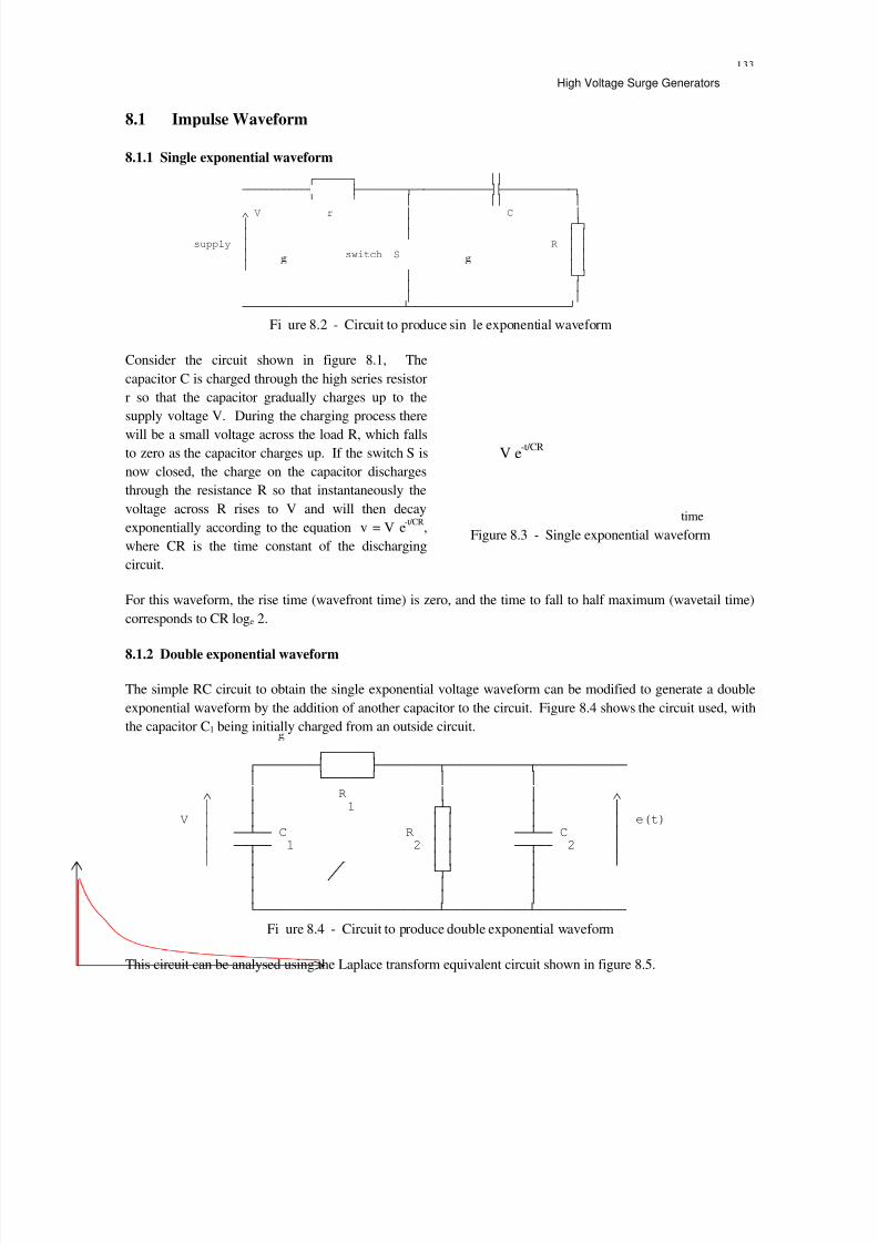
8/6/2019 High Voltage Engineering (Lucas)
http://slidepdf.com/reader/full/high-voltage-engineering-lucas 141/212
High Voltage Surge Generators
8.1 Impulse Waveform
8.1.1 Single exponential waveform
Consider the circuit shown in figure 8.1, The
capacitor C is charged through the high series resistorr so that the capacitor gradually charges up to thesupply voltage V. During the charging process therewill be a small voltage across the load R, which fallsto zero as the capacitor charges up. If the switch S isnow closed, the charge on the capacitor dischargesthrough the resistance R so that instantaneously thevoltage across R rises to V and will then decayexponentially according to the equation v = V e -t/CR ,where CR is the time constant of the dischargingcircuit.
For this waveform, the rise time (wavefront time) is zero, and the time to fall to half maximum (wavetail time)corresponds to CR log e 2.
8.1.2 Double exponential waveform
The simple RC circuit to obtain the single exponential voltage waveform can be modified to generate a doubleexponential waveform by the addition of another capacitor to the circuit. Figure 8.4 shows the circuit used, withthe capacitor C 1 being initially charged from an outside circuit.
This circuit can be analysed using the Laplace transform equivalent circuit shown in figure 8.5.
HFFFFFFI GG
FFFFFFFFFFFM LFFFFFFFFNFFFFFFFFFFFFFMLFFFFFFFFFFFFI JFFFFFFK G GG G
∧ V r G & G G G HOI G G G G
supply G 5 G G G VZLWFK 6 G G G G G
G JNK G G G G
FFFFFFFFFFFFFFFFFFFFFFFFFFFOFFFFFFFFFFFFFFFFFFFFFFFFFFFK
Fi ure 8.2 - Circuit to produce sin le exponential waveform
V e -t/CR
time
Figure 8.3 - Single exponential waveform
HFFFFFFI
HFFFFFFFFM LFFFFFFFFNFFFFFFFFFFFNFFFFFFFFFFFF G JFFFFFFK G G
∧ G 5 G G ∧ G G 1 HOI G G
V G G G G G G H W G FFOFF & 5 G G FFOFF & G G FFNFF G G FFNFF G G G G G G G
G JNK G G G G G G G JFFFFFFFFFFFFFFFFFFFFFFFFOFFFFFFFFFFFOFFFFFFFFFFFF
Fi ure 8.4 - Circuit to produce double exponential waveform

8/6/2019 High Voltage Engineering (Lucas)
http://slidepdf.com/reader/full/high-voltage-engineering-lucas 142/212
High Voltage Engineering - J R Lucas, 2001
If . DQG DUH WKH VROXWLRQV RI WKH HTXDWLRQ
R1 R2 C1 C2 s2
+ (C 1 R1 + C 1 R2 + C 2 R2) s + 1 = 0
then the Laplace transform expression can be simplified as follows.
It is seen that the output waveform is of the double exponential form required.
For a 1/50 V ZDYHIRUP LW FDQ EH VKRZQ WKDW. ≈ DQG≈ ZKHQ W LV LQV $OVR IRU WKH VWDQGDUV ,(& ZDYHIRUP. ≈ DQG≈4.87.
i(s)HFFFFFFI
HFFF! FFFFM LFFFFFFFFNFFFFFFFFFFFNFFFFFFFFFFFF G JFFFFFFK GL V GL V
1 FFFOFFF 5 G G ∧ C s FFFNFFF HOI G G
1 G G G G 1 G ( V
G 5 G G FFOFF G 2 G G FFNFF & V G V G G G G s JNK G
G - G G G G G JFFFFFFFFFFFFFFFFFFFFFFFFOFFFFFFFFFFFOFFFFFFFFFFFF
Fi ure 8.5 - La lace e uivalent circuit for double ex onential
)e-e( -
1 .
RC
V = e(t) givesThis t-t-
12
β α
α β
β α α β β α
+s1
- +s
1 .
-1
.C R
V =
)+)(s+(s1
.C R
V = E(s)
2121
1+s)RC+RC+RC(+sCCRRRCV
= R.(s)i = E(s) givesonsubstituti
sV
= )C
CR +sRCR+sC
1 +R+R(.(s)i
(s)i.sRC = (s)i Also
sV
= )sC
1 +R(.(s)i+)
sC
1 +R+R(.(s)i
(s)i+(s)i = (s)i also
2211212
2121
2121
22221
1121
1222
112
1121
21
∴
∴
,sC
1 .(s)i = R.(s)i = (s) E
R.(s)i+ R.(s)i+sC
1 .(s)i =
sV
2221
2111
This circuit can be analysed in the following manner.

8/6/2019 High Voltage Engineering (Lucas)
http://slidepdf.com/reader/full/high-voltage-engineering-lucas 143/212

8/6/2019 High Voltage Engineering (Lucas)
http://slidepdf.com/reader/full/high-voltage-engineering-lucas 144/212
High Voltage Engineering - J R Lucas, 2001
From equations (1) and (2) it is seen that the wavefront time t 1 is determined predominantly by DQG WKHZDYHWDLO WLPH SUHGRPLQDQWO\ E\.
. DQG DUH WKH VROXWLRQV RI WKH IROORZLQJ TXDGUDWLF HTXDWLRQ LQ V
Since LV D IXQFWLRQ RI 5 1, and . LV D IXQFWLRQ RI 5 2, the effect of R 1 will be to determine the rate of rise of voltage across the load, and thus the wavefront time. It is thus known as the wavefront control resistance.
The maximum voltage available at the output is given by
Thus the maximum (peak) voltage available at the output will depend on the ratio of C 2 to C 1, and on the
charging voltage. If C 2 is low compared to C 1, then we can have a higher voltage peak. The voltage efficiencyof the impulse generator can be approximately be estimated as C 1 /(C 1 + C 2) multiplied by a factor of about 0.95(to account for approximations made in the analysis).
The wavefront control resistance can be connected either outside or within the impulse generator, or partlywithin and partly outside.
8.1.4 Definition of Wavefront and Wavetail times of practical waveforms
In practical impulse waveforms, the initial region and near the peak in the voltage are not very well defined.
Also, near zero and near the peak, the rate of change is quite often much less than in the rest of the wavefront.Hence the wavefront time is not well defined. It is thus usual to define the wavefront by extrapolation based ona rise time for a specific change (say 10% to 90% or in even from 30% to 90% when the initial region is notclear). Figure 8.8 shows how the measurement of this rise time is made.
(4)-----
R)C+C(
1
(3)----- CCRC+C
thatso ,R << R generally
RC+R)C+c(
1
« CCRR
CR+R)C+C( = + also
,CCRR
1 = . thatso
221
211
21
21
11221
2121
11221
2121
≈
≈
≈∴
≈
α
β
α
α β β β α
β α
0 = 1+s.]C R+ R)C +C ([+sC C R R 11221
2
2121
C +C C .V
RC )C +C (C C RV
= RC
V = E
21
1
1221
211
12
≈β max

8/6/2019 High Voltage Engineering (Lucas)
http://slidepdf.com/reader/full/high-voltage-engineering-lucas 145/212

8/6/2019 High Voltage Engineering (Lucas)
http://slidepdf.com/reader/full/high-voltage-engineering-lucas 146/212

8/6/2019 High Voltage Engineering (Lucas)
http://slidepdf.com/reader/full/high-voltage-engineering-lucas 147/212
High Voltage Surge Generators
The wavefront time t f and the wavetail time t t may be evaluated as follows.
Defining the wavefront from 10 % to 90 % and considering only that GHWHUPLQHV WKH ZDYHIURQW
It can also be shown that if the wavefront is considered from 30 % to 90 %, the corresponding expressionbecomes
Similarly, defining the wavetail time as the time to decay to 50 % of peak, and considering only that .
determines the wavetail,
8.2 Operation of Impulse Generator
8.2.1 Uncontrolled operation
In the simplest form of the single stage impulse generator, shown in figure 8.12, the high direct voltage requiredis obtained from a high voltage transformer through a high voltage rectifier. The direct voltage need not besmooth as it only has to charge the first capacitor to peak value. A sphere gap is used as the switch, and as thecharge on the capacitor builds up, so does the voltage across the sphere gap.
CR2.75 = t .e.i
2.75 =
2.197x1.25 = )t-t(1.25 = t .e.i
2.3026 = (0.1)log
1 - = t ,
0.1054 = (0.9)log
1 - = t thatso
22f
abf
ebea
η
β β
β β β β
β β
e = 0.9-1 ,e = 0.1-1
)t -t (1.25 = 0.1-0.9
)t -t ( = t
t -t -
abab
f
ba
C R3.243 = t 22 f η
η
α α α
CR0.693 = t Thus
0.693 = t giving ,
t
0.5log - = thatso
11t
tt
e ,e = 0.5 t - t
sphere gap HFFFFFFFI HFFFFFF LFFFFFFFNFFFF FFFFFFNFFFFM LFFFNFFFFFFFFF G G G JFFFFFFFK G
FFFFF GLRGH G G 5 G ¿ G HOI G G H
a.c. G G G G G FFOFF& 5 G G & FFOFF G
supply FFNFF G G FFNFF G G G G G G G JNK G
FFFFF G G G G G G
JFFFFFFFFFFFFFFFFFOFFFFFFFFFFFFFFOFFFFFFFFFFFFFFFFOFFFFFFFFF h.v. transformer
Fi ure 8.12 - Circuit for uncontrolled operation

8/6/2019 High Voltage Engineering (Lucas)
http://slidepdf.com/reader/full/high-voltage-engineering-lucas 148/212

8/6/2019 High Voltage Engineering (Lucas)
http://slidepdf.com/reader/full/high-voltage-engineering-lucas 149/212

8/6/2019 High Voltage Engineering (Lucas)
http://slidepdf.com/reader/full/high-voltage-engineering-lucas 150/212
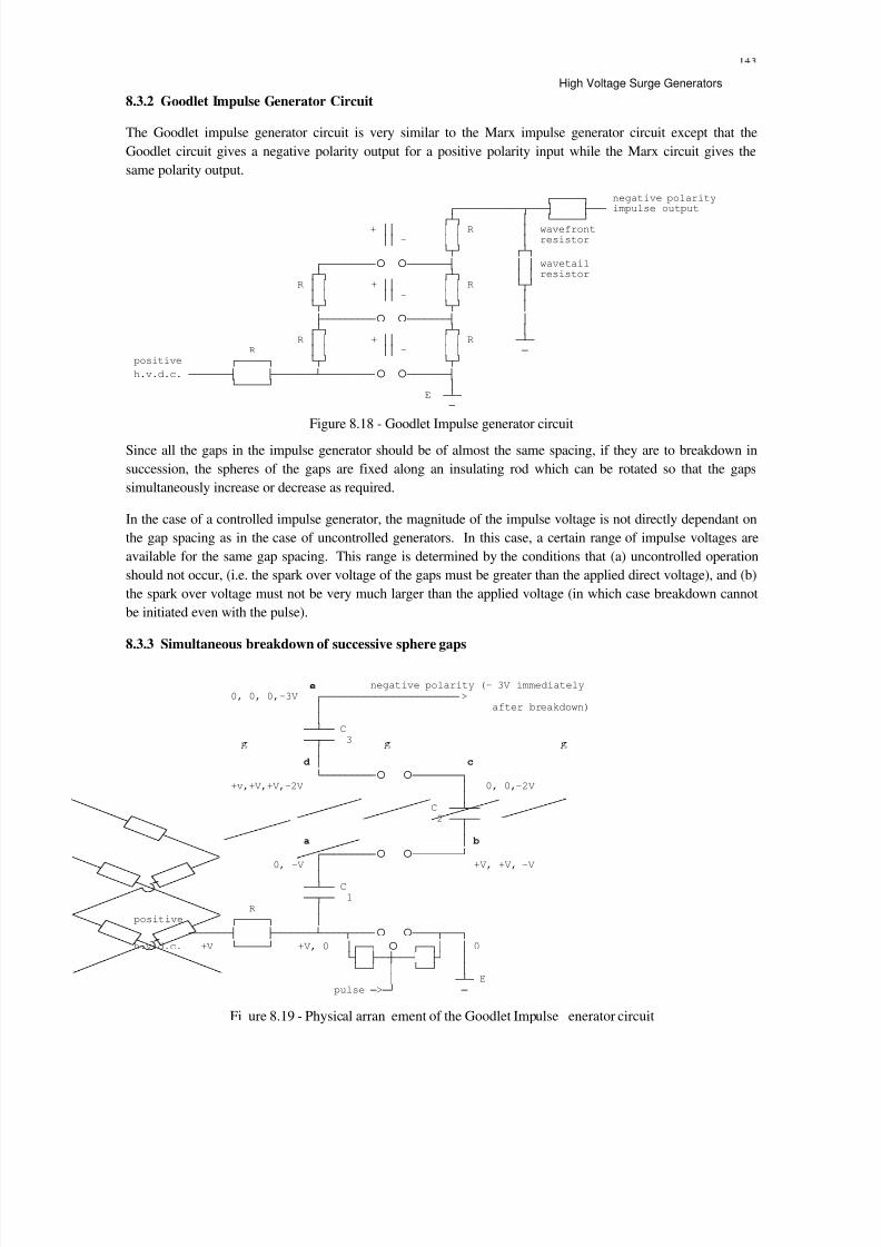
8/6/2019 High Voltage Engineering (Lucas)
http://slidepdf.com/reader/full/high-voltage-engineering-lucas 151/212
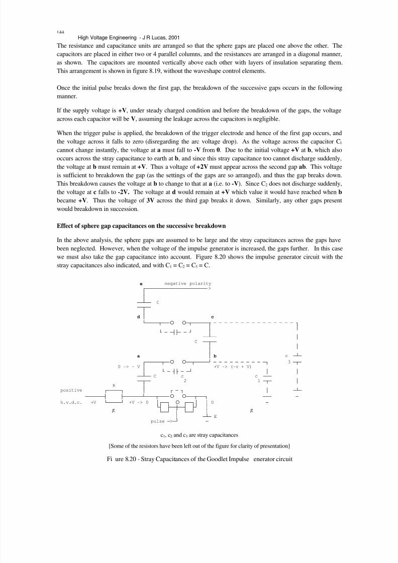
8/6/2019 High Voltage Engineering (Lucas)
http://slidepdf.com/reader/full/high-voltage-engineering-lucas 152/212
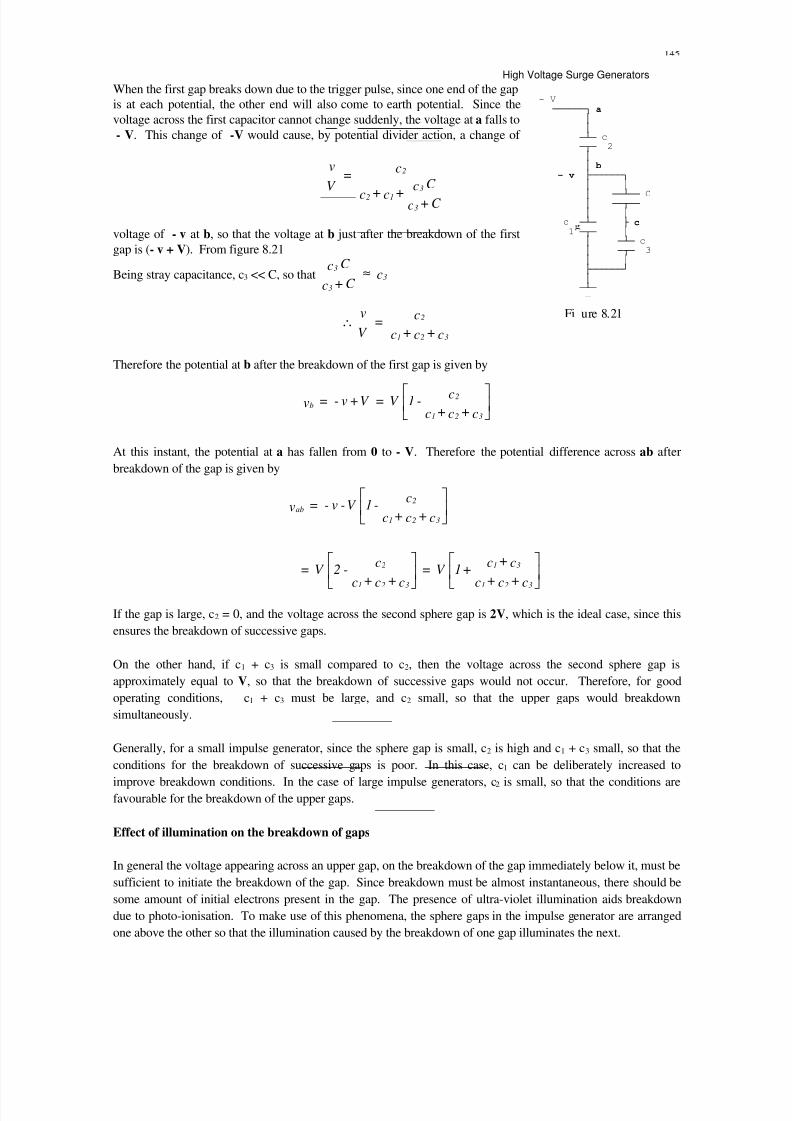
8/6/2019 High Voltage Engineering (Lucas)
http://slidepdf.com/reader/full/high-voltage-engineering-lucas 153/212
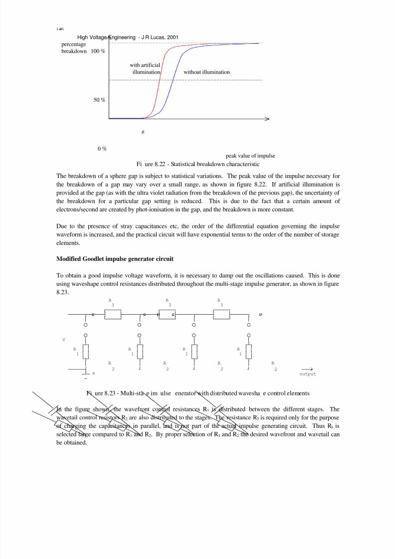
8/6/2019 High Voltage Engineering (Lucas)
http://slidepdf.com/reader/full/high-voltage-engineering-lucas 154/212

8/6/2019 High Voltage Engineering (Lucas)
http://slidepdf.com/reader/full/high-voltage-engineering-lucas 155/212
8/6/2019 High Voltage Engineering (Lucas)
http://slidepdf.com/reader/full/high-voltage-engineering-lucas 156/212

8/6/2019 High Voltage Engineering (Lucas)
http://slidepdf.com/reader/full/high-voltage-engineering-lucas 157/212

8/6/2019 High Voltage Engineering (Lucas)
http://slidepdf.com/reader/full/high-voltage-engineering-lucas 158/212

8/6/2019 High Voltage Engineering (Lucas)
http://slidepdf.com/reader/full/high-voltage-engineering-lucas 159/212

8/6/2019 High Voltage Engineering (Lucas)
http://slidepdf.com/reader/full/high-voltage-engineering-lucas 160/212
High Voltage Engineering - J R Lucas, 2001
Now, the dielectric losses per cubic centimetre in a given material and at a given temperature, are directlyproportional to the frequency of the electric field and to the square of the field strength. Hence the decrease inbreakdown voltage with increasing time of application and increasing temperature and also the dependence of this voltage upon the shape, size, and material of the electrodes and upon the form the electric field.
The measurement of dielectric loss in insulating materials are very important, as they give a fair indication as tocomparative dielectric strengths of such materials. In the case of cable, dielectric loss measurements are nowgenerally recognized as the most reliable guide to the quality and condition of the cable.
9.2.2 Determination of dielectric strength of solid dielectrics
A sheet or disc of the material of not less than 10cm in diameter, is takenand recessed on both sides so as to accommodate the spherical electrodes(2.5 cm in diameter) with a wall or partition of the material between them0.5mm thick. The electrical stress is applied to the specimen by means of the two spheres fitting into the recesses without leaving any clearance,especially at the centre. The applied voltage is of approximately sinewaveform at 50Hz. This voltage is commenced at about 1/3 the full valueand increased rapidly to the full testing voltage.
Sometimes insulators after manufacture are found to contain flaws in the form of voids or air spots.These spots(due to non-homogeneity) have a lower breakdown strength than the material itself, and if present wouldgradually deteriorate and cause ultimate breakdown after a number of years.
High degree ionisations caused in these spots would give rise to high energy electrons which would bombard the
rest of the material, causing physical decomposition. In plastic type of materials,there might be carbonizations,polymerisations, chemical decomposition etc.,which would gradually diffuse into the material the by-products,causing chemical destruction.
The useful life of a component using such material will depend on the weak spots and the applied voltage. If theapplied voltage is small, the life of the component is longer. From design considerations the voltage to beapplied if a particular life span is required can be calculated.The schering bridge type of measurement gives an average type of measurement,where the p.f. and the powerloss indicates the value over the whole of the length.Thus small flaws if present would not cause much of avariation in the overall p.f. Thus in the schering bridge type of measurement such flaws would not be brought
out.
The loss factor of a material does not vary much forlow voltages, but as the voltage is increased at acertain value it starts increasing at a faster rate. Thisis the long time safe working voltage, since beyondthis, the specimen would keep on deteriorating.
If the apparatus need be used only for a short period,the applied voltage can be higher than this safevalue.
In a long length of cable, the greater part of the cablewould be in good conditions but with a few weak spots here and there.
dielectric
material
spherical
electrode
Figure 9.3 - solid sample
loss factortan δ
maximum safeworking voltage
applied voltage
Fi ure 9.4 - variation of loss factor

8/6/2019 High Voltage Engineering (Lucas)
http://slidepdf.com/reader/full/high-voltage-engineering-lucas 161/212
High Voltage Testing
In a Schering bridge type of measurement, since it measures the overall loss, such small individual spots cannotbe detected. It is necessary that such spots are detected as these increase with time and finally cause itsbreakdown.
In high voltage transformers also there might be such small discharges occurring which would not be measuredby the schering bridge.
The method is to apply suitable high voltage to sample, and subject it to a number of duty cycles ( heat cycles,make and break cycles). Discharges caused are made to give pulses to a high frequency amplifier. Thedischarges caused are observed before and after such duty cycles to see whether there is any appreciable increasein the pulse intensity after the cycle of operation. The methods of discussion have been discussed in an earlierchapter.
9.3 Impulse Testing
These are done as tests on sample of apparatus. The impulse test level is determined by the operating level (4 to5 times the normal operating value ) Apply on to the sample a certain number (say 10) positive impulse and 10negative impulses of this particular value. They should withstand this voltage without any destruction.
To test the ultimate impulse strength, apply increasing amounts of impulse voltage until destruction occurs;during the tests it is necessary to see whether there is any damage. The damage may not be immediately visible,so we have it on a high frequency ( single sweep and high speed ) oscilloscope.In the event of complete damage, breakdown of the insulator due to the application of the impulse voltage willbe indicated as in (i). If the insulator has suffered only a minor damage the wave form would show no distortion, but would show as in (ii). If there is no damage caused due to the impulse, the waveform will be complete andundistorted as in (iii).
In testing high voltage insulators whose actual breakdown is in air (i.e flashover takes place before breakdown of insulator) the porcelain itself can be tested by immersing the whole insulator in liquid of high permeability sothat there would be no outside flashover, and actual breakdown of the insulator would occur.
o dielectric
conductoro
<--- weak spots
o
Fi ure 9.5 - sam le of cable showin weak s ots
Figure 9.6 - Observed impulse waveforms
v
t(i)
v
t(ii)
v
t(iii)

8/6/2019 High Voltage Engineering (Lucas)
http://slidepdf.com/reader/full/high-voltage-engineering-lucas 162/212

8/6/2019 High Voltage Engineering (Lucas)
http://slidepdf.com/reader/full/high-voltage-engineering-lucas 163/212
High Voltage Testing
This type of characteristic is important in designing insulators.If a rod gap is to protect a transformer. Then thebreakdown voltage characteristic of the rod gap must be less than that of the transformer so as to protect it. If thecharacteristic cross, protection will be offered only in the region where the rod gap characteristic is lower thanthat of the transformer.
System Voltage I.E.C.Impulse Withstand Voltage
11 kV 75 kV
33 kV 170 kV
66 kV 325 kV
132 kV 550 kV
275 kV 1050 kV
In obtaining the breakdown characteristic of a transformer we do not attempt such tests that cause totaldestruction on transformers as they are expensive. What is done is we take a sample of the material used asinsulators for the transformers and then apply these tests till puncture takes place. Thus the transformercharacteristic is obtained by such tests on samples.
To obtain one point on the voltage vs time lag characteristic we would have to do a large number of tests andtake the mean,as these values vary from sample to sample. The sample would have to be surrounded by a liquidmaterial of high permittivity so that external flashover would not occur.
The impulse test voltage recommended by I.E.C. (International Electrotechnical Commission) are given in thetable 9.1.
The recommendation is that device when subjected to this voltage should not suffer permanent damage or minorpartial damage. The voltage is set at slightly less than the withstand voltage and gradually increase to test value.About 10 positive impulses and 10 negative impulses are applied.
9.4 Voltage Distribution in a Transformer Winding
Consider the entering of an impulse voltage on the terminating transformer, as shown in figure 9.11.
voltage
t
Figure 9.10 - Time lag characteristic

8/6/2019 High Voltage Engineering (Lucas)
http://slidepdf.com/reader/full/high-voltage-engineering-lucas 164/212
High Voltage Engineering - J R Lucas, 2001
Due to the presence of the interwinding capacitance and the capacitances to earth of the transformer windings,the upper elements of the transformer windings tend to be more heavily stressed than the lower portions.
Due to the velocity of propagation of the impulse voltage would not be evenly distributed in the winding. Due tosharp rise of the voltage of the surge. there is a large difference of voltage caused in the winding as the wavefront travels up the winding. Thus there would be an overvoltage across adjacent windings.
Depending on the termination, there will be reflections at the far end of the winding. If the termination is a shortcircuit, at the lowest point the voltage wave whose amplitude is same as the original wave but of oppositepolarity is reflected. For a line which is open circuited, the reflected wave would be of the same magnitude and
of the same sign.
Arising out of the reflections at the far end , there would be some coils heavily stressed. The position of theheavily stressed coils depending on the velocity of propagation.
If flashover occurs at the gap (lightning arrestor) the voltage of the impulse suddenly drops to zero whenflashover occurs. This can be represented by a full wave, and a negative wave starting from the time flashoveroccurs. The chopped wave, though it reduces the voltage of the surge to zero, will have a severe effect of thewinding due to sharp drop in the voltage. Thus it is always necessary to subject the transformer during tests tochopped wave conditions. Generally the method is to apply full-waves and see whether damage has occurredand then to apply the chopped waves and to see whether damage has occurred and then to apply the choppedwaves and to see whether damage has occurred.
Example
A rectangular voltage V is impressed at the line terminal of a winding of a high voltage transformer , the neutralpoint being isolated from earth.The capacitance to earth of the complete winding is Cw.Prove that the voltage ata point in the winding distant X from the neutral is
If C g = 900 pF and Cw = 10 pF , calculate the ratio of the maximum initial voltage gradient in the winding to theaverage voltage gradient.How will the initial voltage distribution in the winding be effected if the wavefront hasa duration of several microseconds ?
Fi ure 9.11 - Sur e propa ation in transformer windin
windingof length=l ,C
C =a wherecosh
cosh
w
g2 ,a
xla
.V = v x
lightningarrestor
transformer winding
voltage
t i m e
surge

8/6/2019 High Voltage Engineering (Lucas)
http://slidepdf.com/reader/full/high-voltage-engineering-lucas 165/212

8/6/2019 High Voltage Engineering (Lucas)
http://slidepdf.com/reader/full/high-voltage-engineering-lucas 166/212

8/6/2019 High Voltage Engineering (Lucas)
http://slidepdf.com/reader/full/high-voltage-engineering-lucas 167/212
High Voltage Testing
(d) One-minute Rain test : The insulator is sprayed throughout the test with artificial rain drawn from a sourceof supply at a temperature within 10 o C of the ambient temperature of the neighbourhood of the insulator. Therain is sprayed at an angle of 45 o on the insulator at the prescribed rate of 3 mm/minute. The resistivity of thewater should be 100 ohm-m ± 10%. The prescribed voltage is maintained for one minute.
Wet flash-over test : The voltage shall then be increased gradually until flash-over occurs. This is repeatedten times. There shall be no damage to the insulator.
(e) Visible discharge test : This states that after the room has been darkened and the specified test voltageapplied, after five minutes, there should be no visible signs of corona.
9.5.2 Sample Tests
The sample is tested fully, up to and including the point of breakdown. This is done only on a few samples of the insulator.
(a) Temperature cycle test : The complete test shall consist of five transfers (hot-cold-hot-....), each transfernot exceeding 30 s.
(b) Mechanical loading test : The insulator shall be mechanically loaded up to the point of failure. Whenfailure occurs, the load should not be less than 2000 lbf.
(c) Electro-mechanical test : The insulator is simultaneously subjected to electrical and mechanical stress. (i.e.it shall be subjected to a power frequency voltage and a tensile force simultaneously. The voltage shall be 75%of dry flash-over voltage of the unit. There should be no damage caused.
(d) Overvoltage test : The insulator shall be completely immersed in an insulating medium (oil), to preventexternal flashover occurring. The specified overvoltage must be reached without puncture. The voltage is thengradually increased until puncture occurs.
(e) Porosity test : Freshly broken pieces of porcelain shall show no dye penetration after having been immersedfor 24 hours in an alcoholic mixture of fushing at a pressure of 2000 p.s.i.
9.5.3 Routine Tests
These are to be applied to all insulators and shall be commenced at a low voltage and shall be increased rapidlyuntil flash-over occurs every few seconds. The voltage shall be maintained at this value for a minimum of fiveminutes, or if failures occur, for five minutes after the last punctured piece has been removed. At the conclusionof the test the voltage shall be reduced to about one-third of the test voltage before switching off.
Mechanical Routine Test: A mechanical load of 20% in excess of the maximum working load of the insulatoris applied after suspending the insulator for one minute. There should be no mechanical failure of the insulator.

8/6/2019 High Voltage Engineering (Lucas)
http://slidepdf.com/reader/full/high-voltage-engineering-lucas 168/212

8/6/2019 High Voltage Engineering (Lucas)
http://slidepdf.com/reader/full/high-voltage-engineering-lucas 169/212
High Voltage Testing
Since the chopped wave test exertsconsiderable stress on the winding, there issome controversy on the requirement of thistest.
Thus the chopped wave requirement is notuniversal. In the American industry, thechopped wave is conducted at 150% fullwave and such that the chopping is done atless than the peak value. In this case thestress might in fact be very much more thanin the British method.
9.7 Tests on Cables
For cables not in the supper voltage class the tests to be carried out are laid down in the appropriate Britishstandard specifications.
Thus for paper impregnated insulated cables with lead or alloy sheaths, BS 480 Part I: 1954, the tests (purelyelectrical) are as follows;
(1) Acceptance Tests at Works
(a) Conductor resistance
(b) Voltage test : The applied voltage must be of approximately sinusoidal shape and of any frequency between25 and 100 Hz. It must be increased gradually to the full value and maintain continuously for 15 minutesbetween conductors and between each conductors and sheath. The required values of the test voltages aretabulated in the specification and, as one illustration of the magnitude relative to the normal voltages, the figuresfor the 11 kV cables for earthed system are given in the table.
VoltageDesignation
Belted Cables Single-core, S.L.& Screened Cables
(i) (ii) (ii)
(1) (2) (1) (2) (1) (2)11 kV 24 kV 36 kV 14 kV 21 kV 15 kV 22 kV
where (i) Between conductors, (ii) Between any conductor and sheath(1) Cable as manufactured, (2) After bending test
It will be seen that a voltage test is made before and after a bending test. In this the cable has to be bent around acylinder of specified diameter to make one complete turn: it is then unwound and the process repeated in theopposite direction . The cycle of process has to be carried out three times.
(c) Dielectric power-factor / Voltage test (for 33 kV cables only) :
Each core of every drum of completed cable is tested for dielectric power factor at room temperature at thefollowing a.c. single phase 50 Hz voltages : 9.5 kV , 19 kV , 28.5 kV, 38.0 kV.
Fi ure 9.15 - cho ed waveform at 150% volta e
100%
150%
0t

8/6/2019 High Voltage Engineering (Lucas)
http://slidepdf.com/reader/full/high-voltage-engineering-lucas 170/212

8/6/2019 High Voltage Engineering (Lucas)
http://slidepdf.com/reader/full/high-voltage-engineering-lucas 171/212
High Voltage Testing
9.8 Tests on High Voltage Bushings
9.8.1 Bushing
A single or composite structure carrying a conductor or providing passage for a conductor, through a partition,such as a wall or tank cover, or through a ring type current transformer and insulating it there from, it includesthe means of attachment to the partition.
(i) Solid Bushing : A bushing consisting of a single piece of solid insulating material which is continuousbetween its outer surface and the inner conducting surface, which may be the main conductor or a conductinglayer connected thereto.
(ii) Plain Bushing: A bushing consisting of a single piece of solid insulating material, with a space betweenthe conductor and the inner surface of the solid insulation. The space is occupied by air, oil or other insulating
medium which forms part of the insulation. [See item (iii)]
(iii) Oil filled Bushing: A bushing consisting of an oil-filled insulating shell, the oil providing the major radialinsulation.[Note: The conductor may be further insulated by a series of spaced concentric cylinders which may be providedwith cylindrical conducting layers with the object of controlling the internal and external electric fields.]
(iv) Condenser busing : A bushing in which cylindrical conducting layers are arranged coaxially with theconductor within a solid body of insulating materials, (including materials impregnated with oils or otherimpregnants),the lengths and diameters of the cylinders being designed with the object of controlling the internaland external electric fields
[Note:A conductor bushing may be provided with a weather shield, in which case the intervening space may befilled with oil or other insulating medium.it is recommended that the term condenser bushing with oil filling beused for this type.]
9.8.2 Tests on Bushings
Rating of bushings: Some of the relevant clauses from the standard is given in the following sections.
Clause 4: A bushing shall be rated in terms of the following:
a) voltage(refer table 1, clause 5)b) normal current (refer tables 2 and 3 clause 6)c) frequency (refer clause 7)d) insulation level (see clause 8 below)
Clause 8: The insulation level of bushing is designed by a voltage which the bushing must be capable of withstanding under the specified test conditions
For impulse tested bushings the rated insulation level is expressed as an impulse voltage value i.e. the impulsewithstand voltage with 1/50 s full wave
For non-impulse tested bushings the rated insulation level is expressed as a power frequency voltage value i.e.one minute dry withstand voltage.
8/6/2019 High Voltage Engineering (Lucas)
http://slidepdf.com/reader/full/high-voltage-engineering-lucas 172/212

8/6/2019 High Voltage Engineering (Lucas)
http://slidepdf.com/reader/full/high-voltage-engineering-lucas 173/212

8/6/2019 High Voltage Engineering (Lucas)
http://slidepdf.com/reader/full/high-voltage-engineering-lucas 174/212
10
Insulation Co-ordination
10.0 Insulation Co-ordination
The term Insulation Co-ordination was originally introduced to arrange the insulation levels of the severalcomponents in the transmission system in such a manner that an insulation failure, if it did occur, would be
confined to the place on the system where it would result in the least damage, be the least expensive to repair,and cause the least disturbance to the continuity of the supply. The present usage of the term is broader.Insulation co-ordination now comprises the selection of the electric strength of equipment in relation to thevoltages which can appear on the system for which the equipment is intended. The overall aim is to reduce toan economically and operationally acceptable level the cost and disturbance caused by insulation failure andresulting system outages.
To keep interruptions to a minimum, the insulation of the various parts of the system must be so graded thatflashovers only occur at intended points. With increasing system voltage, the need to reduce the amount of insulation in the system, by proper co-ordination of the insulating levels become more critical.
10.1 Terminology
Nominal System Voltage : It is the r.m.s. phase-to-phase voltage by which a system is designated
Maximum System Voltage : It is the maximum rise of the r.m.s. phase-to-phase system voltage
For the nominal system voltages used in Sri Lanka, the international maximum system voltages are shown intable 10.1.
Nominal System Voltage (kV) 11 33 66 132 220
Maximum System Voltage (kV) 12 36 72.5 145 245
Table 10.1
Factor of Earthing : This is the ratio of the highest r.m.s. phase-to-earth power frequency voltage on a soundphase during an earth fault to the r.m.s. phase-to-phase power frequency voltage which would be obtained at
the selected location without the fault.This ratio characterises, in general terms, the earthing conditions of a system as viewed from the selected faultlocation.

8/6/2019 High Voltage Engineering (Lucas)
http://slidepdf.com/reader/full/high-voltage-engineering-lucas 175/212
Insulation Co-ordination
Effectively Earthed System : A system is said to be effectively earthed if the factor of earthing does notexceed 80%, and non-effectively earthed if it does.[Note: Factor of earthing is 100% for an isolated neutral system, while it is 57.7% (corresponding to 1/ %3) fora solidly earthed system. In practice, the effectively earthed condition is obtained when the ratio x 0 /x1 < 3and the ratio r 0 /x1 < 1.
Insulation Level : For equipment rated at less than 300 kV, it is a statement of the Lightning impulse withstandvoltage and the short duration power frequency withstand voltage.
For equipment rated at greater than 300 kV, it is a statement of the Switching impulse withstand voltage andthe power frequency withstand voltage.
Conventional Impulse Withstand Voltages : This is the peak value of the switching or lightning impulse testvoltage at which an insulation shall not show any disruptive discharge when subjected to a specified number of applications of this impulse under specified conditions.
Conventional Maximum Impulse Voltage : This is the peak value of the switching or lightning overvoltagewhich is adopted as the maximum overvoltage in the conventional procedure of insulation co-ordination.
Statistical Impulse Withstand Voltage : This is the peak value of a switching or lightning impulse testvoltage at which insulation exhibits, under the specified conditions, a 90% probability of withstand. Inpractice, there is no 100% probability of withstand voltage. Thus the value chosen is that which has a 10%probability of breakdown.
Statistical Impulse Voltage : This is the switching or lightning overvoltage applied to equipment as a result of
an event of one specific type on the system (line energising, reclosing, fault occurrence, lightning discharge,etc), the peak value of which has a 2% probability of being exceeded.
Figure 10.1 - Statistical Impulse Withstand Voltage
Probabilitydensity
2% probability
statistical Occurrence ofovervoltage overvoltage
Fi ure 10.2 - Statistical Impulse Volta e
100%breakdownprobability
statisticalwithstand voltage
appliedvoltage
10%0

8/6/2019 High Voltage Engineering (Lucas)
http://slidepdf.com/reader/full/high-voltage-engineering-lucas 176/212
High Voltage Engineering - J R Lucas, 2001
Rated Short Duration Power Frequency Withstand Voltage : This is the prescribed r.m.s. value of sinusoidal power frequency voltage that the equipment shall withstand during tests made under specifiedconditions and for a specific time, usually not exceeding one minute.
Protective Level of Protective Device : These are the highest peak voltage value which should not beexceeded at the terminals of a protective device when switching impulses and lightning impulses of standardshape and rate values are applied under specific conditions.
10.2 Conventional method of insulation co-ordination
In order to avoid insulation failure, the insulation level of different types of equipment connected to the systemhas to be higher than the magnitude of transient overvoltages that appear on the system. The magnitude of transient over-voltages are usually limited to a protective level by protective devices. Thus the insulation levelhas to be above the protective level by a safe margin. Normally the impulse insulation level is established at a
value 15-25% above the protective level.
Consider the typical co-ordination of a 132 kV transmission line between the transformer insulation, a line gap(across an insulator string) and a co-ordinating gap (across the transformer bushing).
[Note: In a rural distribution transformer, a lightning arrester may not be used on account of the high cost and aco-ordinating gap mounted on the transformer bushing may be the main surge limiting device]
Maximum Protection0 System Voltage Level
voltage increasing
Nominal Maximum Sound InsulationSystem Voltage Phase voltage Withstand Level
Figure 10.3 - Co-ordination using gaps
transformer
Crest voltage(MV)
transformer insulation1.0m line gap0.66 mm co-ord. gap
t (µs)

8/6/2019 High Voltage Engineering (Lucas)
http://slidepdf.com/reader/full/high-voltage-engineering-lucas 177/212
Insulation Co-ordination
In co-ordinating the system under consideration, we have to ensure that the equipment used are protected, andthat inadvertent interruptions are kept to a minimum. The co-ordinating gap must be chosen so as to provideprotection of the transformer under all conditions. However, the line gaps protecting the line insulation can beset to a higher characteristic to reduce unnecessary interruptions.
A typical set of characteristics for insulation co-ordination by conventional methods, in which lightningimpulse voltages are the main source of insulation failure, is shown in the figure 1.3.
For the higher system voltages, the simple approach used above is inadequate. Also, economic considerationsdictate that insulation co-ordination be placed on a more scientific basis.
10.3 Statistical Method of Insulation Co-ordination
At the higher transmission voltages, the length of insulator strings and the clearances in air do not increaselinearly with voltage but approximately to V 1.6 The required number of suspension units for different
overvoltage factors is shown.
It is seen that the increase in the number of discunits is only slight for the 220 kV system, with
the increase in the overvoltage factor from 2.0 to3.5, but that there is a rapid increase in the 750kV system. Thus, while it may be economicallyfeasible to protect the lower voltage lines up toan overvoltage factor of 3.5 (say), it is definitelynot economically feasible to have an overvoltagefactor of more than about 2.0 or 2.5 on the highervoltage lines. In the higher voltage systems, it isthe switching overvoltages that is predominant.However, these may be controlled by properdesign of switching devices.
Figure 10.4 - Requirement of number of units for different voltages
Probability %
99959080
50
20
105
10.1
0.01
1.0 1.5 2.0 2.5 3.0 3.5
overvoltage (pu)Figure 10.5 Probability of overvoltage exceeding abscissae
overvoltage factor (p.u.)
750kV 500 kV
345 kV
220 kV
Required No.of Units
60
50
40
30
20
10
0
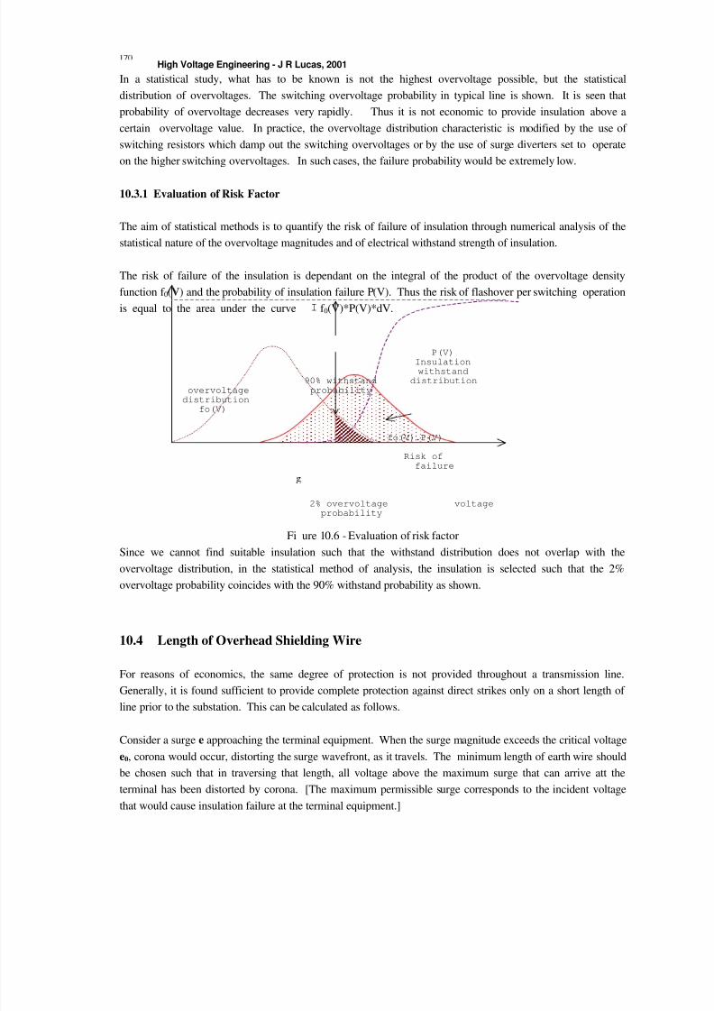
8/6/2019 High Voltage Engineering (Lucas)
http://slidepdf.com/reader/full/high-voltage-engineering-lucas 178/212

8/6/2019 High Voltage Engineering (Lucas)
http://slidepdf.com/reader/full/high-voltage-engineering-lucas 179/212
Insulation Co-ordination
10.4.1 Modification of Waveshape by Corona
When a surge voltage wave travelling on an overhead line causes an electric field around it exceeding thecritical stress of air, corona will be formed. This corona formation obviously extracts the energy required fromthe surge. Since the power associated with corona increases as the square of the excess voltage, the attenuationof the waveform will not be uniform so that the waveform gets distorted. Further, corona increases theeffective radius of the conductor giving rise to a greater capacitance for the outer layers. Since the lineinductance remains virtually a constant, the surge associated with the outer layers of corona would have a lowerwave velocity than in the conductor itself. These effects in practice give rise to a wavefront distortion and not awavetail distortion, as shown in figure 10.7.
Corona thus reduces the steepness of the wavefront above the critical voltage, as the surge travels down theline. This means that energy is lost to the atmosphere.
Now consider the mathematical derivation.
Energy associated with a surge waveform = i L+eC 2212
21
But the surge voltage e is related to the surge current i by the equation
eC = i L i.e. LC
e = Z
e = i 2
212
21 ,
0
So that the total wave energy = eC 2
Consider the figure 10.8. Let the voltage at a point P at position x be e at time t.
Then voltage at point P 1 just behind P would be x xe
-e δ ∂∂
at time t, or t..v.-e x
e
δ ∂∂
If the voltage is above corona inception, it would not remain at this value but would attain a value t +e t e δ ∂
∂ at P
at time t+ ∆t , when the surge at P 1 moves forward to P 2.
Figure 10.7 - Modification of waveshape due to corona
Figure 10.8 - Propagation of Surge
(e) (d) (c) (b) (a) undistorted waveform
time increasing criticalvolta e e o
e
velocity v
P1 P2
P e
t t e
e δ ∂∂+ x
xe
e δ ∂∂−
(position, time) P1 (x - δx, t) P 2 (x, t + δt)(x, t) (x+ δx, t+ δt)

8/6/2019 High Voltage Engineering (Lucas)
http://slidepdf.com/reader/full/high-voltage-engineering-lucas 180/212
High Voltage Engineering - J R Lucas, 2001
[Note: t e
xe , ∂
∂∂∂ would in fact be negative quantities on the wavefront.]
Thus corona causes a depression in the voltage from t)v-(e xe δ ∂
∂ to t)+(e t e δ ∂
∂ , with a corresponding loss of
energy of t)+(e-t)v-(eC t e 2
xe 2 δ δ ∂
∂∂∂ or t +v2Ce- t
e xe δ ∂
∂∂∂ .
The energy to create a corona field is proportional to the square of the excess voltage. i.e. k(e - e 0)2.
Thus the energy required to change the voltage from e to t)+(e t e δ ∂
∂ is given by
)e-(e-)e-t +(ek 02
0t e 2δ ∂
∂ or t )e-2k(e t e
0 δ ∂∂ .
The loss of energy causing distortion must be equal to the change in energy required. Thus
Rearranging and simplifying gives the equation
Wave propagation under ideal conditions is written in the form
Thus we see that the wave velocity has decreased below the normal propagation velocity, and that the wavevelocity of an increment of voltage at e has a magnitude given by
Thus the time of travel for an element at e when it travels a distance x is given by
−=−
−+==
eee
C k
v x
v x
v x
ei
eee
C k
v x
v x
t
o
e
o
e
...
1
v x
-v
x
eis the time lag ∆t corresponding to the voltage element at e. Thus
∆ee-1v.C
k = x
t
0
Example 10.1
A transformer has an impulse insulation level of 1050 kV and is to be operated with an insulation margin of 15% under lightning impulse conditions. The transformer has a surge impedance of 1600 S and is connected toa transmission line having a surge impedance of 400 S . A short length of overhead earth wire is to be used forshielding the line near the transformer from direct strikes. Beyond the shielded length, direct strokes on thephase conductor can give rise to voltage waves of the form 1000 e -0.05t kV ( where t is expressed in µs).
If the corona distortion in the line is represented by the expression s/m ee-1
B1 =
xt 0 µ ∆ , where B = 110
m/ µs and e 0 = 200 kV, determine the minimum length of shielding wire necessary in order that the transformerinsulation will not fail due to lightning surges.
t .)e-2k(e=t +v2Ce- t e
0t e
xe δ δ ∂
∂∂∂
∂∂
t e
e)e-(e
.C k
+1-= xe
v 0
∂∂
∂∂
t e
-= xe
v ∂∂
∂∂
ee-e
ck
+1
v =v
0e
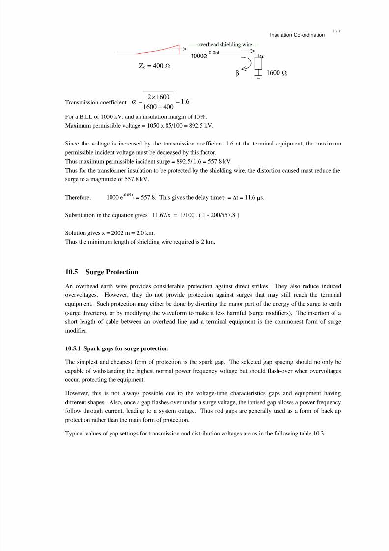
8/6/2019 High Voltage Engineering (Lucas)
http://slidepdf.com/reader/full/high-voltage-engineering-lucas 181/212
Insulation Co-ordination
Transmission coefficient 6.14001600
16002 =+×=α
For a B.I.L of 1050 kV, and an insulation margin of 15%,Maximum permissible voltage = 1050 x 85/100 = 892.5 kV.
Since the voltage is increased by the transmission coefficient 1.6 at the terminal equipment, the maximumpermissible incident voltage must be decreased by this factor.Thus maximum permissible incident surge = 892.5/ 1.6 = 557.8 kV
Thus for the transformer insulation to be protected by the shielding wire, the distortion caused must reduce thesurge to a magnitude of 557.8 kV.
Therefore, 1000 e -0.05 t1 = 557.8. This gives the delay time t 1 = ∆t = 11.6 µs.
Substitution in the equation gives 11.67/x = 1/100 . ( 1 - 200/557.8 )
Solution gives x = 2002 m = 2.0 km.Thus the minimum length of shielding wire required is 2 km.
10.5 Surge Protection
An overhead earth wire provides considerable protection against direct strikes. They also reduce inducedovervoltages. However, they do not provide protection against surges that may still reach the terminalequipment. Such protection may either be done by diverting the major part of the energy of the surge to earth(surge diverters), or by modifying the waveform to make it less harmful (surge modifiers). The insertion of ashort length of cable between an overhead line and a terminal equipment is the commonest form of surgemodifier.
10.5.1 Spark gaps for surge protection
The simplest and cheapest form of protection is the spark gap. The selected gap spacing should no only becapable of withstanding the highest normal power frequency voltage but should flash-over when overvoltagesoccur, protecting the equipment.
However, this is not always possible due to the voltage-time characteristics gaps and equipment havingdifferent shapes. Also, once a gap flashes over under a surge voltage, the ionised gap allows a power frequencyfollow through current, leading to a system outage. Thus rod gaps are generally used as a form of back upprotection rather than the main form of protection.
Typical values of gap settings for transmission and distribution voltages are as in the following table 10.3.
overhead shielding wire
1000 e -0.05t α
β 1600 Ω Zo = 400 Ω

8/6/2019 High Voltage Engineering (Lucas)
http://slidepdf.com/reader/full/high-voltage-engineering-lucas 182/212

8/6/2019 High Voltage Engineering (Lucas)
http://slidepdf.com/reader/full/high-voltage-engineering-lucas 183/212

8/6/2019 High Voltage Engineering (Lucas)
http://slidepdf.com/reader/full/high-voltage-engineering-lucas 184/212
High Voltage Engineering - J R Lucas, 2001
10.5.3 Selection of Surge Diverters
Surge diverters for a particular purpose are selected as follows.
(a) Rated Voltage
The designated maximum permissible r.m.s. value of power frequency voltage between line and earthterminals.
This is generally selected corresponding to 80% of the system phase-to-phase voltage for effectively earthedsystems and corresponding to 100% of the system phase-to-phase voltage for non-effectively earthed systems.[Note: A surge diverter of a higher rating may sometimes have to be chosen if some of the other requiredcriteria are not satisfied by this diverter].
(b) Discharge Current
The surge current that flows through the surge diverter after spark over.
Nominal discharge current: This is the discharge current having a designated crest value and waveshape, whichis used to classify a surge diverter with respect to durability and protective characteristics.
The standard waveform for the discharge current is taken as 8/20 µs).
The nominal value of discharge current is selected from the standard values 10 kA (station type), 5 kA(intermediate line type), 2.5 kA (distribution type) and 1.5 kA (secondary type), depending on the application.The highest ratings are used for the protection of major power stations, while the lowest ratings are used inrural distribution systems. The above nominal discharge currents are chosen based on statisticalinvestigations which have shown that surge diverter currents at the station has the following characteristic.
99 % of discharge currents are less than 10 kA95 % of discharge currents are less than 5 kA90 % of discharge currents are less than 3 kA70 % of discharge currents are less than 1 kA50 % of discharge currents are less than 0.5 kA
(c) Discharge Voltage (or Residual voltage)
The Discharge voltage is the voltage that appears between the line and earth terminals of the surge diverterduring the passage of discharge currents.
The discharge voltage of the selected arrestor should be below the BIL of the protected equipment by a suitablemargin (generally selected between 15% and 25%).
The discharge voltage of an arrestor at nominal discharge current is not a constant, but also depends on the rateof rise of the current and the waveshape. Typically, an increase of the rate of rise from 1 kA/ µs to 5 kA/ µswould increase the discharge voltage by only about 35 %.
The dependence of the discharge voltage on the discharge current is also small. Typically, an increase of discharge current from 5 kA to 10 kA would increase the discharge voltage by about 15% for Silicon Carbidearrestors and by about 2% for Zinc Oxide arrestors. The discharge voltage is more often referred to as theresidual discharge voltage].
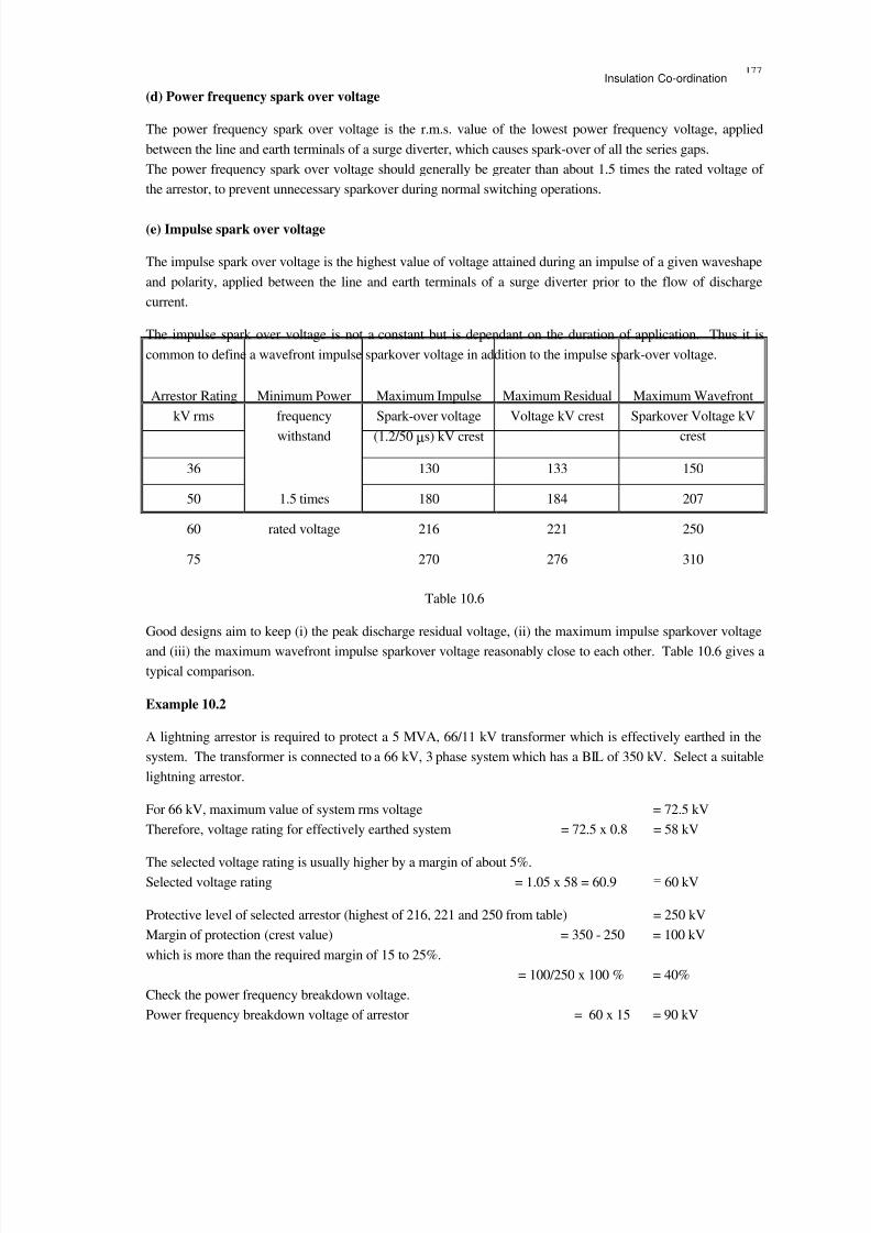
8/6/2019 High Voltage Engineering (Lucas)
http://slidepdf.com/reader/full/high-voltage-engineering-lucas 185/212
Insulation Co-ordination
(d) Power frequency spark over voltage
The power frequency spark over voltage is the r.m.s. value of the lowest power frequency voltage, appliedbetween the line and earth terminals of a surge diverter, which causes spark-over of all the series gaps.The power frequency spark over voltage should generally be greater than about 1.5 times the rated voltage of
the arrestor, to prevent unnecessary sparkover during normal switching operations.
(e) Impulse spark over voltage
The impulse spark over voltage is the highest value of voltage attained during an impulse of a given waveshapeand polarity, applied between the line and earth terminals of a surge diverter prior to the flow of dischargecurrent.
The impulse spark over voltage is not a constant but is dependant on the duration of application. Thus it iscommon to define a wavefront impulse sparkover voltage in addition to the impulse spark-over voltage.
Arrestor RatingkV rms
Minimum Powerfrequencywithstand
Maximum ImpulseSpark-over voltage(1.2/50 µs) kV crest
Maximum ResidualVoltage kV crest
Maximum WavefrontSparkover Voltage kV
crest
36 130 133 150
50 1.5 times 180 184 207
60 rated voltage 216 221 250
75 270 276 310
Table 10.6
Good designs aim to keep (i) the peak discharge residual voltage, (ii) the maximum impulse sparkover voltageand (iii) the maximum wavefront impulse sparkover voltage reasonably close to each other. Table 10.6 gives atypical comparison.
Example 10.2
A lightning arrestor is required to protect a 5 MVA, 66/11 kV transformer which is effectively earthed in the
system. The transformer is connected to a 66 kV, 3 phase system which has a BIL of 350 kV. Select a suitablelightning arrestor.
For 66 kV, maximum value of system rms voltage = 72.5 kVTherefore, voltage rating for effectively earthed system = 72.5 x 0.8 = 58 kV
The selected voltage rating is usually higher by a margin of about 5%.Selected voltage rating = 1.05 x 58 = 60.9 = 60 kV
Protective level of selected arrestor (highest of 216, 221 and 250 from table) = 250 kVMargin of protection (crest value) = 350 - 250 = 100 kV
which is more than the required margin of 15 to 25%.= 100/250 x 100 % = 40%
Check the power frequency breakdown voltage.Power frequency breakdown voltage of arrestor = 60 x 15 = 90 kV
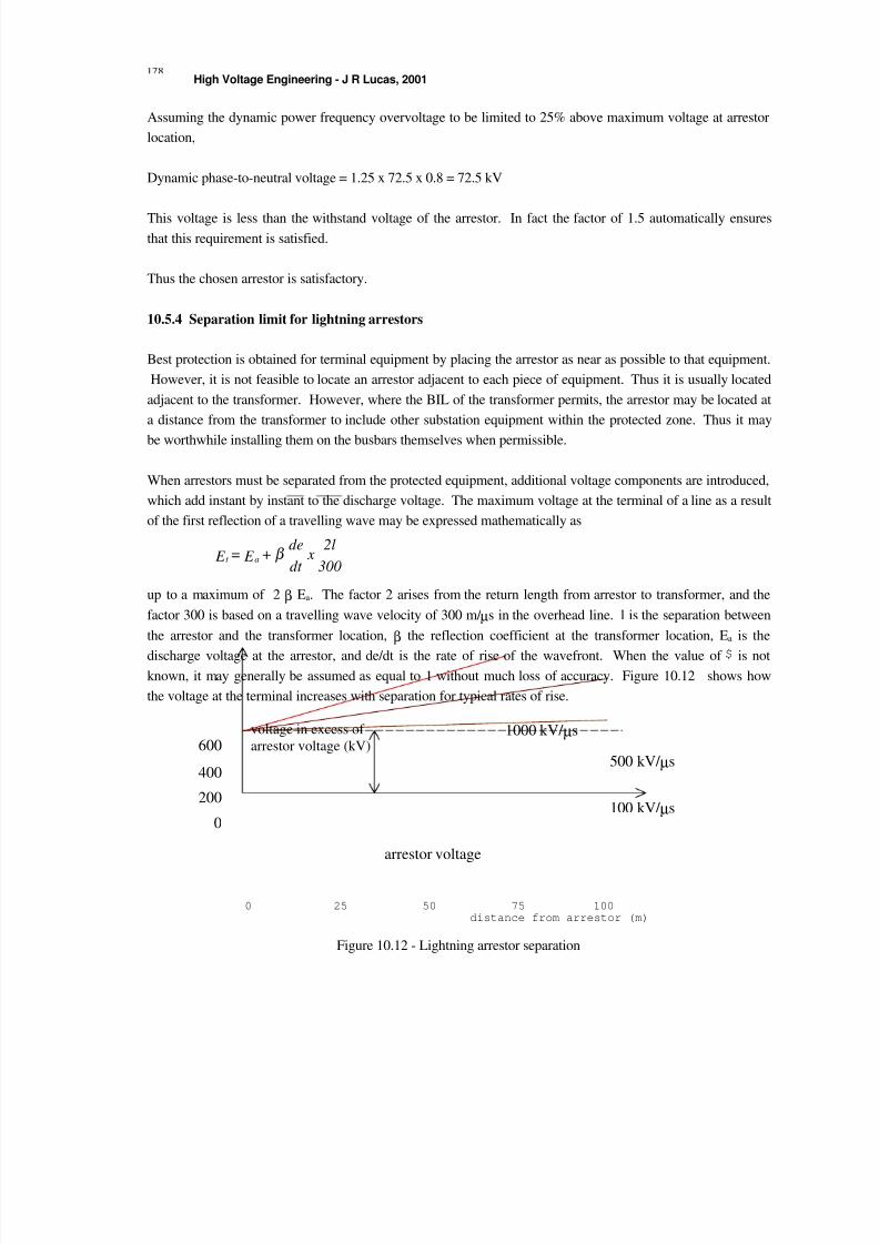
8/6/2019 High Voltage Engineering (Lucas)
http://slidepdf.com/reader/full/high-voltage-engineering-lucas 186/212

8/6/2019 High Voltage Engineering (Lucas)
http://slidepdf.com/reader/full/high-voltage-engineering-lucas 187/212
Insulation Co-ordination
Example 10.3
A 500 kV steep fronted wave (rate of rise 1000 kV/ µs) reaches a transformer of surge impedance 1600 S through a line of surge impedance 400 S and protected by a lightning arrestor with a protective spark-over levelof 650 kV, 90 m from the transformer. Sketch the voltage waveforms at the arrestor location and at thetransformer location. Sketch also the waveforms if the separation is reduced to 30 m.
If the separation is 90 m, travel time of line J = 90/300 = 0.3 µsTransmission coefficient α = 2 . 1600 = 1.6
1600+400Reflection coefficient β = 1.6 - 1 = 0.6
The voltage waveforms at the arrestor location and at the transformer location can be sketched as follows.
0.2 0.4 0.6 0.8 1.0 1.2 t ( µs)
0.2 0.4 0.6 0.8 1.0 1.2 t ( µs)
α
β
transformer
Zo=1600 Ω
Zo = 400 Ω
500 kV
90 m
arrestor
800
600
400
200
0
Ea (kV)
spark over
residual discharge voltage
incident wave
2 τ
800
600
400
200
0
Et (kV)
spark over
incident wave
τ
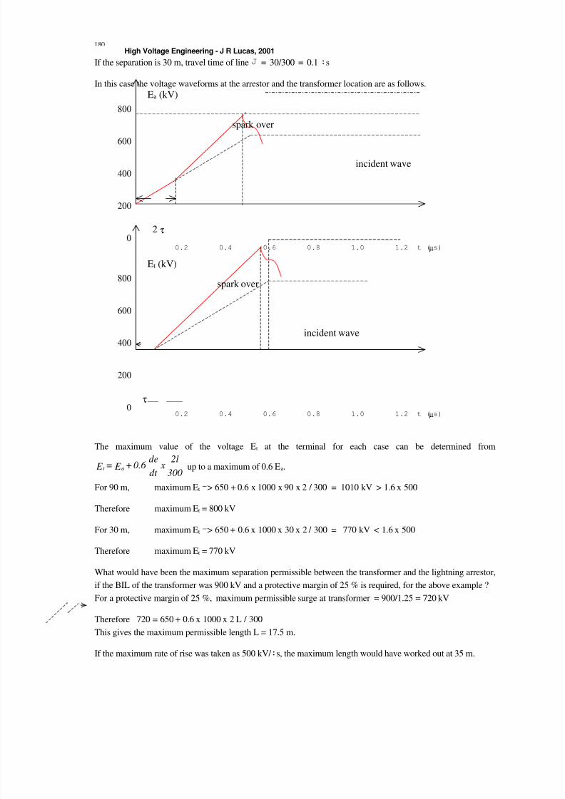
8/6/2019 High Voltage Engineering (Lucas)
http://slidepdf.com/reader/full/high-voltage-engineering-lucas 188/212
High Voltage Engineering - J R Lucas, 2001
If the separation is 30 m, travel time of line J = 30/300 = 0.1 : s
In this case the voltage waveforms at the arrestor and the transformer location are as follows.
The maximum value of the voltage E t at the terminal for each case can be determined from
3002l
xdt de
0.6 + E = E at up to a maximum of 0.6 E a.
For 90 m, maximum E t - > 650 + 0.6 x 1000 x 90 x 2 / 300 = 1010 kV > 1.6 x 500
Therefore maximum E t = 800 kV
For 30 m, maximum E t - > 650 + 0.6 x 1000 x 30 x 2 / 300 = 770 kV < 1.6 x 500
Therefore maximum E t = 770 kV
What would have been the maximum separation permissible between the transformer and the lightning arrestor,if the BIL of the transformer was 900 kV and a protective margin of 25 % is required, for the above example ?For a protective margin of 25 %, maximum permissible surge at transformer = 900/1.25 = 720 kV
Therefore 720 = 650 + 0.6 x 1000 x 2 L / 300This gives the maximum permissible length L = 17.5 m.
If the maximum rate of rise was taken as 500 kV/ : s, the maximum length would have worked out at 35 m.
0.2 0.4 0.6 0.8 1.0 1.2 t ( µs)
0.2 0.4 0.6 0.8 1.0 1.2 t ( µs)
800
600
400
200
0
Ea (kV)
spark over
incident wave
2 τ
800
600
400
200
0
Et (kV)
spark over
incident wave
τ
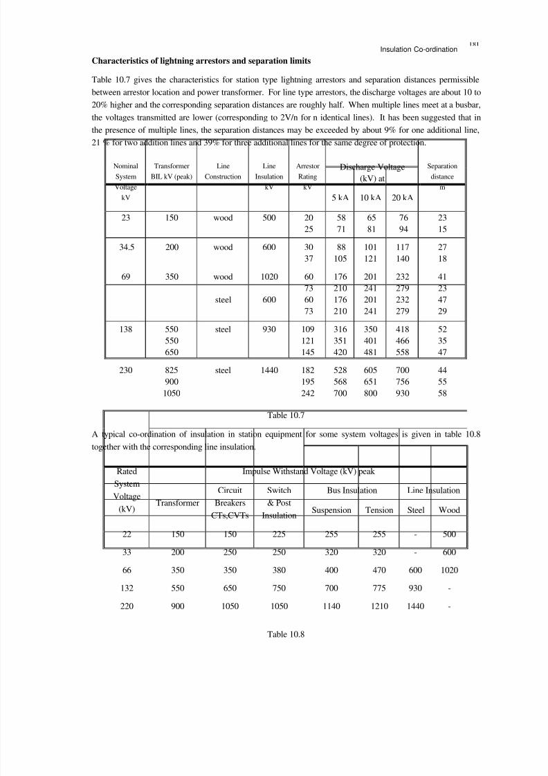
8/6/2019 High Voltage Engineering (Lucas)
http://slidepdf.com/reader/full/high-voltage-engineering-lucas 189/212
Insulation Co-ordination
Characteristics of lightning arrestors and separation limits
Table 10.7 gives the characteristics for station type lightning arrestors and separation distances permissiblebetween arrestor location and power transformer. For line type arrestors, the discharge voltages are about 10 to20% higher and the corresponding separation distances are roughly half. When multiple lines meet at a busbar,
the voltages transmitted are lower (corresponding to 2V/n for n identical lines). It has been suggested that inthe presence of multiple lines, the separation distances may be exceeded by about 9% for one additional line,21 % for two addition lines and 39% for three additional lines for the same degree of protection.
Discharge Voltage(kV) at
NominalSystemVoltage
kV
TransformerBIL kV (peak)
LineConstruction
LineInsulation
kV
ArrestorRating
kV 5 kA 10 kA 20 kA
Separationdistance
m
23 150 wood 500 2025
5871
6581
7694
2315
34.5 200 wood 600 3037
88105
101121
117140
2718
69 350 wood
steel
1020
600
60736073
176210176210
201241201241
232279232279
41234729
138 550550650
steel 930 109121145
316351420
350401481
418466558
523547
230 825900
1050
steel 1440 182195242
528568700
605651800
700756930
445558
Table 10.7
A typical co-ordination of insulation in station equipment for some system voltages is given in table 10.8together with the corresponding line insulation.
Impulse Withstand Voltage (kV) peak
Bus Insulation Line Insulation
RatedSystemVoltage
(kV)Transformer
CircuitBreakers
CTs,CVTs
Switch& Post
InsulationSuspension Tension Steel Wood
22 150 150 225 255 255 - 500
33 200 250 250 320 320 - 600
66 350 350 380 400 470 600 1020
132 550 650 750 700 775 930 -
220 900 1050 1050 1140 1210 1440 -
Table 10.8
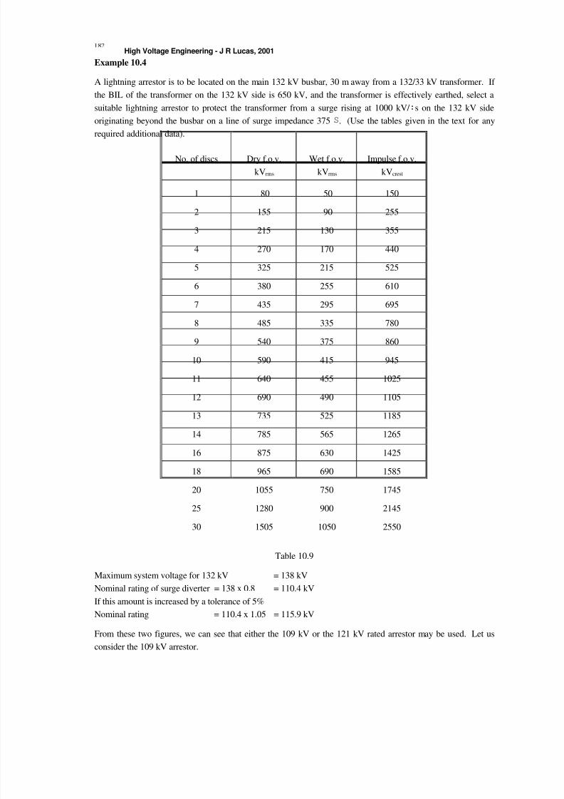
8/6/2019 High Voltage Engineering (Lucas)
http://slidepdf.com/reader/full/high-voltage-engineering-lucas 190/212
High Voltage Engineering - J R Lucas, 2001
Example 10.4
A lightning arrestor is to be located on the main 132 kV busbar, 30 m away from a 132/33 kV transformer. If the BIL of the transformer on the 132 kV side is 650 kV, and the transformer is effectively earthed, select asuitable lightning arrestor to protect the transformer from a surge rising at 1000 kV/ : s on the 132 kV side
originating beyond the busbar on a line of surge impedance 375 S . (Use the tables given in the text for anyrequired additional data).
No. of discs Dry f.o.v.kV rms
Wet f.o.v.kV rms
Impulse f.o.v.kV crest
1 80 50 150
2 155 90 255
3 215 130 355
4 270 170 440
5 325 215 525
6 380 255 610
7 435 295 695
8 485 335 780
9 540 375 860
10 590 415 945
11 640 455 1025
12 690 490 1105
13 735 525 1185
14 785 565 1265
16 875 630 1425
18 965 690 1585
20 1055 750 174525 1280 900 2145
30 1505 1050 2550
Table 10.9
Maximum system voltage for 132 kV = 138 kVNominal rating of surge diverter = 138 x 0.8 = 110.4 kVIf this amount is increased by a tolerance of 5%
Nominal rating = 110.4 x 1.05 = 115.9 kV
From these two figures, we can see that either the 109 kV or the 121 kV rated arrestor may be used. Let usconsider the 109 kV arrestor.

8/6/2019 High Voltage Engineering (Lucas)
http://slidepdf.com/reader/full/high-voltage-engineering-lucas 191/212

8/6/2019 High Voltage Engineering (Lucas)
http://slidepdf.com/reader/full/high-voltage-engineering-lucas 192/212
11High Voltage
Direct Current Transmission
11.0 Historical Background
Power Transmission was initially carried out in the early 1880s using Direct Current ( d.c. ). With theavailability of transformers (for stepping up the voltage for transmission over long distances and for steppingdown the voltage for safe use), the development of robust induction motor (to serve the users of rotary power),the availability of the superior synchronous generator, and the facilities of converting a.c. to d.c. whenrequired, a.c. gradually replaced d.c. However in 1928, arising out of the introduction of grid control to the
mercury vapour rectifier around 1903, electronic devices began to show real prospects for high voltage directcurrent (HVDC) transmission, because of the ability of these devices for rectification and inversion. The mostsignificant contribution to HVDC came when the Gotland Scheme in Sweden was commissioned in 1954 to bethe World's first commercial HVDC transmission system. This was capable of transmitting 20 MW of powerat a voltage of -100 kV and consisted of a single 96 km cable with sea return.
With the fast development of converters (rectifiers and inverters) at higher voltages and larger currents, d.c.transmission has become a major factor in the planning of the power transmission. In the beginning all HVDCschemes used mercury arc valves, invariably single phase in construction, in contrast to the low voltagepolyphase units used for industrial application. About 1960 control electrodes were added to silicon diodes,giving silicon-controlled-rectifiers (SCRs or Thyristors).
In 1961 the cross channel link between England and France was put into operation. The a.c. systems wereconnected by two single conductor submarine cables (64km) at ± 100kV with two bridges each rated at 80MW. The mid-point of the converters was grounded at one terminal only so as not to permit ground currents toflow. Sea return was not used because of its effect on the navigation of ships using compasses. The link is anasynchronous link between the two systems with the same nominal frequency (60Hz).
The Sakuma Frequency Changer which was put into operation in 1965, interconnects the 50Hz and the 60Hzsystems of Japan. It is the first d.c. link of zero length, and is confined to a single station. It is capable of transmitting 300 MW in either direction at a voltage of 250 kV.
In 1968 the Vancouver Island scheme was operated at +250 kV to supply 300 MW and is the first d.c. link operating in parallel with an a.c. link.
In 1970 a solid state addition (Thyristors) was made to the Gotland scheme with a rating of 30MW at -150kV.
Also in 1970 the Kingsnorth scheme in England was operated on an experimental basis. In this schemetransmission of power by underground d.c. cable at ± 200 kV, 640 MW is used to reinforce the a.c. systemwithout increasing the interrupting duty of a.c. circuit breakers.
The first converter station using exclusively Thyristors was the Eel River scheme in Canada. Commissioned in1972, it supplies 320 MW at 80 kV d.c. The link is of zero length and connects two a.c. systems of the samenominal frequency (60Hz).

8/6/2019 High Voltage Engineering (Lucas)
http://slidepdf.com/reader/full/high-voltage-engineering-lucas 193/212
High Voltage Direct Current Transmission 185
The largest thyristors used in converter valves have blocking voltages of the order of kilovolts and currents of the order 100s of amperes. In order to obtain higher voltages the thyristor valve uses a single series string of these thyristors. With higher current ratings required, the valve utilizes thyristors directly connected in parallelon a common heat sink.
The largest operational converter stations have ratings of the order of gigawatts and operate at voltages of 100sof kilovolts, and maybe up to 1000 km in length.
The thyristors are mostly air cooled but may be oil cooled, water cooled or Freon cooled. With air cooled andoil cooled thyristors the same medium is used as insulant. With the Freon cooled thyristors, SF6 may be usedfor insulation, leading to the design of a compact thyristor valve.
Unlike an a.c. transmission line which requires a transformer at each end, a d.c. transmission line requires aconvertor at each end. At the sending end rectification is carried out, where as at the receiving end inversion iscarried out.
11.1 Comparison of a.c and d.c transmission
11.1.1 Advantages of d.c.
(a) More power can be transmitted per conductor per circuit.
The capabilities of power transmission of an a.c. link and a d.c. link are different.For the same insulation, the direct voltage V d is equal to the peak value ( √2 x rms value) of the alternating
voltage V d.Vd = √2 V a
For the same conductor size, the same current can transmitted with both d.c. and a.c. if skin effect is notconsidered.
Id = Ia
Thus the corresponding power transmission using 2 conductors with d.c. and a.c. are as follows.
d c power per conductor P d = V d Id
a c power per conductor P a = V a Ia cos 3
The greater power transmission with d.c. over a.c. is given by the ratio of powers.
H Pd = _√2__ = G DW S I XQLW\ Pa cos 3 G DW S I
J In practice, a.c. transmission is carried out using either single circuit or double circuit 3 phase transmissionusing 3 or 6 conductors. In such a case the above ratio for power must be multiplied by 2/3 or by 4/3 .
In general, we are interested in transmitting a given quantity of power at a given insulation level, at a givenefficiency of transmission. Thus for the same power transmitted P, same losses P L and same peak voltage V,we can determine the reduction of conductor cross-section A d over A a.

8/6/2019 High Voltage Engineering (Lucas)
http://slidepdf.com/reader/full/high-voltage-engineering-lucas 194/212

8/6/2019 High Voltage Engineering (Lucas)
http://slidepdf.com/reader/full/high-voltage-engineering-lucas 195/212
High Voltage Direct Current Transmission 187
Also, the absence of continuous charging current in a d.c. cable permits higher active power transfer, especiallyover long lengths.
(Charging current of the order of 6 A/km for 132 kV). Critical length at 132 kV ≈80 km for a.c cable. Beyond
the critical length no power can be transmitted without series compensation in a.c. lines. Thus derating whichis required in a.c. cables, thus does not limit the length of transmission in d.c.
A comparison made between d.c. and a.c. for the transmission of about 1550 MVA is as follows. Six numbera.c. 275 kV cables, in two groups of 3 cables in horizontal formation, require a total trench width of 5.2 m,whereas for two number d.c. ±500 kV cables with the same capacity require only a trench width of about 0.7 m.
(e) No skin effect
Under a.c. conditions, the current is not uniformly distributed over the cross section of the conductor. The
current density is higher in the outer region (skin effect) and result in under utilisation of the conductor cross-section. Skin effect under conditions of smooth d.c. is completely absent and hence there is a uniform currentin the conductor, and the conductor metal is better utilised.
(f) Less corona and radio interference
Since corona loss increases with frequency (in fact it is known to be proportional to f+25 ), for a givenconductor diameter and applied voltage, there is much lower corona loss and hence more importantly less radiointerference with d.c. Due to this bundle conductors become unnecessary and hence give a substantial savingin line costs. [Tests have also shown that bundle conductors would anyway not offer a significant advantagefor d.c as the lower reactance effect so beneficial for a.c is not applicable for d.c.]
(g) No Stability Problem
The d.c. link is an asynchronous link and hence any a.c. supplied through converters or d.c. generation do nothave to be synchronised with the link. Hence the length of d.c. link is not governed by stability.
In a.c. links the phase angle between sending end and receiving end should not exceed 30 o at full-load fortransient stability (maximum theoretical steady state limit is 90 o).
Note: θ = w √OF SHU NP [ [5) rad/km ≈ (2 x 180 x 50)/(3 x 10 5) ≈ 0.06 0 /km
The phase angle change at the natural load of a line is thus 0.6 o per 10 km.
The maximum permissible length without compensation ≈ 30/0.06 = 500 km
With compensation, this length can be doubled to 1000 km.
(h) Asynchronous interconnection possible
With a.c. links, interconnections between power systems must be synchronous. Thus different frequencysystems cannot be interconnected. Such systems can be easily interconnected through hvdc links. For different
frequency interconnections both convertors can be confined to the same station.
In addition, different power authorities may need to maintain different tolerances on their supplies, even thoughnominally of the same frequency. This option is not available with a.c. With d.c. there is no such problem.

8/6/2019 High Voltage Engineering (Lucas)
http://slidepdf.com/reader/full/high-voltage-engineering-lucas 196/212
High Voltage Engineering - J R Lucas, 2001188
(i) Lower short circuit fault levels
When an a.c. transmission system is extended, the fault level of the whole system goes up, sometimesnecessitating the expensive replacement of circuit breakers with those of higher fault levels. This problem can
be overcome with hvdc as it does not contribute current to the a.c. short circuit beyond its rated current. In factit is possible to operate a d.c. link in "parallel" with an a.c. link to limit the fault level on an expansion. In theevent of a fault on the d.c line, after a momentary transient due to the discharge of the line capacitance, thecurrent is limited by automatic grid control. Also the d.c. line does not draw excessive current from the a.c.system.
(j) Tie line power is easily controlled
In the case of an a.c. tie line, the power cannot be easily controlled between the two systems. With d.c. tielines, the control is easily accomplished through grid control. In fact even the reversal of the power flow is just
as easy.
11.1.2 Inherent problems associated with hvdc
(a) Expensive convertors
Expensive Convertor Stations are required at each end of a d.c. transmission link, whereas only transformerstations are required in an a.c. link.
(b) Reactive power requirement
Convertors require much reactive power, both in rectification as well as in inversion. At each convertor thereactive power consumed may be as much at 50% of the active power rating of the d.c. link. The reactivepower requirement is partly supplied by the filter capacitance, and partly by synchronous or static capacitorsthat need to be installed for the purpose.
(c) Generation of harmonics
Convertors generate a lot of harmonics both on the d.c. side and on the a.c. side. Filters are used on the a.c.side to reduce the amount of harmonics transferred to the a.c. system. On the d.c. system, smoothing reactors
are used. These components add to the cost of the convertor.
(d) Difficulty of circuit breaking
Due to the absence of a natural current zero with d.c., circuit breaking is difficult. This is not a major problemin single hvdc link systems, as circuit breaking can be accomplished by a very rapid absorbing of the energyback into the a.c. system. (The blocking action of thyristors is faster than the operation of mechanical circuitbreakers). However the lack of hvdc circuit breakers hampers multi-terminal operation.
(e) Difficulty of voltage transformation
Power is generally used at low voltage, but for reasons of efficiency must be transmitted at high voltage. Theabsence of the equivalent of d.c. transformers makes it necessary for voltage transformation to carried out onthe a.c. side of the system and prevents a purely d.c. system being used.

8/6/2019 High Voltage Engineering (Lucas)
http://slidepdf.com/reader/full/high-voltage-engineering-lucas 197/212

8/6/2019 High Voltage Engineering (Lucas)
http://slidepdf.com/reader/full/high-voltage-engineering-lucas 198/212
High Voltage Engineering - J R Lucas, 20011 0
11.2 Convertor arrangements and operation
The three-phase six-valve bridge rectifier is almost exclusively used in high voltage direct current applications.This is shown in figure 11.2.
The 6-valve bridge connection gives double the direct voltage as output compared to the simple 3-phaserectifier. The convertor transformer may either be wound star-star as shown, or as star-delta (or even as delta-star or delta-delta). The ripple of each of these connections is the same, but are phase shifted by 30 0 in outputwith respect to each other. To obtain a smoother output, two bridges (one star-star and the other star-delta) maybe connected together to give the twelve pulse connection.
For the 6-valve bridge, with zero firing delay, the voltage waveforms across the thyristors are shown in figure11.3. At any given instant, one thyristor valve on either side is conducting. The conducting period for thethyristor valve R1 is shown on the diagram.
The corresponding d.c. output voltage waveforms are shown in figure 11.4.
It can be shown that for the 6-valve bridge, the total r.m.s. ripple is of the order of 4.2% of the d.c. value (forzero delay . DQG ]HUR FRPPXWDWLRQ 7KH ULSSOH RI FRXUVH LQFUHDVHV ZLWK WKH GHODvalue o I DERXW DW.
star-star convertor transformer Graetz bridge
Fi ure 11.2 - Hexa-valve Brid e Convertor arran ement
R1 Y3 B5 R1
Y6 B2 R4 Y6
Figure 11.3 - Thyristor voltage waveforms ( .
Y6,R1 R1,B2 B2,Y3 Y3,R4 R4,B5 B5,Y6 Y6,R1
Figure 11.4 - d.c. output waveforms ( .
B
Y
R
1 3 5
4 6 2
choke+
−

8/6/2019 High Voltage Engineering (Lucas)
http://slidepdf.com/reader/full/high-voltage-engineering-lucas 199/212
High Voltage Direct Current Transmission 1 1
With the 12 pulse bridge, the r.m.s. ripple is of the order of 1.03% of the d.c. value (for . DQG DQGLQFUHDVHV WR DERXW DW.
The use of a choke reduces the ripple appearing in the direct current transmitted.
If E is the r.m.s. line-to-line voltage, then if .
WKHQ WKH GLUHFW YROWDJH RXWSXW LV JLY(11.1).
11.2.1 Control angle (Delay angle)
The control angle for rectification (also known as the ignition angle) is the angle by which firing is delayedbeyond the natural take over for the next thyristor. The transition could be delayed using grid control. Gridcontrol is obtained by superposing a positive pulse on a permanent negative bias to make the grid positive.Once the thyristor fires, the grid loses control.
Assuming no commutation (2 thyristors on same side conducting simultaneously during transfer), the voltagewaveforms across the thyristors as shown in figure 11.5.
In this case, the magnitude of the direct voltage output is given by the equation (11.2).
11.2.2 Commutation angle (overlap angle)
The commutation period between two thyristors on the same side of the bridge is the angle by which onethyristor commutates to the next. During this period WKH YROWDJH DW WKH HOHFWURGH IROORZV PHD2 conducting thyristors on the same side. This is shown in figure 11.6.
3 x2
3
1 .
23 . E =
d 23
x2 x3
E x2 = V
3
3
-do ∫
π π
θ θ π
π
π
sin
cos
E 1.350= E .23
=V doπ
(11.1)
R1 Y3 B5 R1
Y6 B2 R4 Y6
Fi ure 11.5 - Thyristor volta e waveforms (with delay .
-3
++3
3
1 .
23 . E =
d 23 x2 x
3 E x2 = V
+
+-d
3
3
∫
α π
α π
π
θ θ π
α
α
π
π
sinsin
cos
V = E 23
=V dod α α π
coscos (11.2)
αα

8/6/2019 High Voltage Engineering (Lucas)
http://slidepdf.com/reader/full/high-voltage-engineering-lucas 200/212
High Voltage Engineering - J R Lucas, 20011 2
With both the delay angle and commutation being present, the magnitude of the direct voltage may bedetermined from equation (11.3) as follows.
An alternate method of derivation of the result is based on comparison of similar areas on the waveform.Figure 11.7 gives the necessary information.
d.c. output = average value of waveform
R1 Y3 B5 R1
Figure 11.6 - commutation between 2 thyristors
( ) ∫ ∫
∫
d .+d .+)+( 3
E 23 =
d )( f 23
2 3
E 2 = V
+
++-3 2
21
++-
+-
+
+-d
3
3
3
3
3
3
θ θ θ θ θ π
θ θ π
α
γ α
π γ α
α
α
α
π
π
π
π
π
π
coscoscos
[ ])+(+2
V = V dod γ α α coscos (11.3)
→ . ← → . ← →
→ . ← → . ←
Figure 11.7 - Graphical analysis of waveform
θ θ π
π γ α
γ α
d .)(V 3 / 2
1 =V
3 2 ++
+d ∫
α
γ w
A1 B2
A2
B1
B3 A3
θ = 0 α α+γ 2π/3+α+γ π π+α π+α+γ

8/6/2019 High Voltage Engineering (Lucas)
http://slidepdf.com/reader/full/high-voltage-engineering-lucas 201/212
High Voltage Direct Current Transmission 1 3
In this integral, in graphical form, area A 1 can be replaced by area B 1. Similarly, area A 2 can be replaced byarea B 2 and area A 3 by area B 3. The integral equation then reduces to the form shown below.
where √2 E is the peak value of the line voltage.
Simplification gives the desired result as in equation (11.3).
Commutation is a result of the a.c. system inductance L c, which does not allow the current through a thyristorto extinguish suddenly. Thus the larger the current the larger the commutation angle
If the extinction angle for rectifier operation w is defined as w = . WKHQ 9d can be written as in equation11.4.
Consider the commutation between thyristors 1 & 3 in the bridge circuit shown in figure 11.8. Let i c be thecommutation current. The commutation current is produced by the voltage e c which is the line voltage betweenphases 1 and 2.
This can also be written in the following form, with i c = 0 at the start of commutation and i c = Id at the end of commutation.
[ ])-( - )+( 2
E 23 =
d 2
E 23 =
V
-
+d
α π γ α π
θ θ π
α π
γ α
coscos
sin∫
[ ]
[ ])+(+2
V =
)+(+ 2
E 23 =V
0
d
γ α α
γ α α π
coscos
coscos
Figure 11.8 - Circuit for analysis of commutation
[ ]w+=V 21
d coscos α (11.4)
t E 2=
)3
- t (-)3
+t (3
2 E = E - E =e 12c
ω
π ω
π ω
sin
coscos
1 3 5
4 6 2
+
−
Lc
E1
Lc
E2
ec
ic
Ld Id

8/6/2019 High Voltage Engineering (Lucas)
http://slidepdf.com/reader/full/high-voltage-engineering-lucas 202/212
High Voltage Engineering - J R Lucas, 20011 4
This equation may be integrated as follows to give equation 11.5.
Equation 11.4 can also be written of the form of equation (11.6).
From equations (11.5) and (11.6) w may be eliminated to give the equation (11.7).
It can also be shown that equation (11.7) can be rewritten in terms of the extinction angle w instead of theignition angle . DV LQ HTXDWLRQ
Equation (11.7) suggests that the convertor may be represented by a no load d.c. output voltage Vo cos .
and a series fictitious resistance & / c / as shown in figure 11.9. The fictitious resistor does not however
consume any active power.
t d id
L2=ec
cc
id Le c
I
0cc
+=w
2
1d
=)t (d ∫ ∫ ω ω
γ α
α
I L=)w-(2
E i.e.
I L=)t (d t E 2
d c
d c
w
21
ω α
ω ω ω α
coscos
sin∫
I E
L2 =w- d
cω α coscos (11.5)
V V 2
=w+o
d coscos α (11.6)
V
L3 +
V
V = , E 23
=V
I E 2
L +V V =
0
c
0
d 0
d c
0
d
π ω
α π
ω α
cos
cos
I L3
-V =V d c
0d π
ω α cos∴ (11.7)
I L3
+wV =V d c
0d π
ω cos (11.8)
5 & / c , d HFFFFFFFFI
HFFFFFFFFFFM LFFFFFFFFFF¾ FFF G JFFFFFFFFK ¿ G G G G
9R FRV . FFOFF G FNF G 9 d G G G G G G JFFFFFFFFFFFFFFFFFFFFFFFFFFFFFFFFFF
Figure 11.9 - Equivalent circuit for Rectifier

8/6/2019 High Voltage Engineering (Lucas)
http://slidepdf.com/reader/full/high-voltage-engineering-lucas 203/212
High Voltage Direct Current Transmission 1 5
11.2.3 Current Waveforms
If Commutation is not considered, the current waveforms through each thyristor (assuming a very high value of inductance L d in the d.c. circuit to give complete smoothing) is a rectangular pulse lasting exactly one-third of acycle. This is shown in figure 11.10 for the cases without delay and with delay.
When commutation is considered, the rise and fall of the current waveforms would be modified as they wouldno longer be instantaneous, as shown in figure 11.11.
Since each phase has 2 thyristors on the opposite half cycles, the a.c. current waveform on the secondary sideof the transformer has a non-sinusoidal waveform as shown in figure 11.12.
If commutation angle is not considered, we can easily calculate the r.m.s. value of the a.c. current on thetransformer secondary I s as in equation (11.9).
V1 →_. _← V1
I1 Id
. . Figure 11.10 - Thyristor current waveforms (
V1 V1
← → I1 I1
→ ← → ← →. ← → ←
Figure 11.11 - Thyristor current waveforms
V1 V1
I1 I1
→_ _← →|
. ZLWK. DQG
Fi ure 11.12 - Current waveforms on transformer secondar
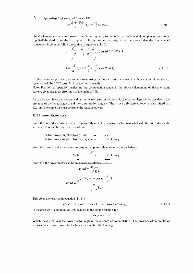
8/6/2019 High Voltage Engineering (Lucas)
http://slidepdf.com/reader/full/high-voltage-engineering-lucas 204/212

8/6/2019 High Voltage Engineering (Lucas)
http://slidepdf.com/reader/full/high-voltage-engineering-lucas 205/212

8/6/2019 High Voltage Engineering (Lucas)
http://slidepdf.com/reader/full/high-voltage-engineering-lucas 206/212
High Voltage Engineering - J R Lucas, 20011 8
Note: During normal operation of the convertor as a rectifier, the delay angle . LV VPDOO DERXW0), while thecommutation angle is comparatively larger (about 20 0).
11.2.6 Inversion
Because the thyristors conduct only in one direction, the current in a convertor cannot be reversed. Powerreversal can only be obtained by the reversal of the direct voltage (average value) V d.
For inversion to be possible, a high value of inductance must be present, and the delay angle . ! 0, since V d changes polarity at this angle. The theoretical maximum delay for inversion would occur at . 0.Thus it is common practice to define a period of advance from this point rather than a delay from the previouscross-over as defined for rectification. Thus we define - . DV WKH LJQLWLRQangle for inversion or the angleRI DGYDQFH 6LPLODUO\ WKH H[WLQFWLRQ DQJOH LV DOVR GHILQHG DV/ - w. The definition of the commutationDQJOH LV XQFKDQJHG 7KXV/
It must be noted, that unlike with rectification which can be operated with.
LQYHUVLRQ FDQQRW EH FDRXW ZLWK VLQFH D PLQLPXP DQJOH/ 0 is required for deionisation of the arc and regaining grid control.
Thus we have the practical relationship / 0 < 3UDFWLFDO YDOXHV RI/ 0 lie between 1 0 and 8 0.
Inversion cannot of course be carried out without a d.c. power source. Further, to obtain the necessaryfrequency for the a.c. on inversion, the commutation voltage is obtained from either synchronous machines orfrom the a.c. system fed. In isolated systems, L C circuits may also be sometimes used for the purpose. Figure11.16 shows the thyristor voltage waveforms for inversion.
During inversion, each thyristor conducts during the negative half cycle, so that the direct voltage waveformand the corresponding current has the form shown in figure 11.17.
R4 Y6 B2
β B5 γ δ R1 Y3
α
Fi ure 11.16 - Th ristor volta e waveforms for inversion
Fi ure 11.17 - Direct volta e waveform & thyristor current waveform

8/6/2019 High Voltage Engineering (Lucas)
http://slidepdf.com/reader/full/high-voltage-engineering-lucas 207/212
High Voltage Direct Current Transmission 1
The equations derived earlier for the convertor are valid. However, they are usually written in terms of thevariables DQG/ LQVWHDG RI. DQG Z 7KXV WKH HTXDWLRQ 9d = ½ V 0 [cos . FRV. @ EHFRPHV
Vd = ½ V 0 [cos ( - FRV - / @
or (-) V d = ½ V 0 [cos FRV/@ 90 cos &/ c / ,d
Since the direct voltage is always negative during inversion, it is common practice to omit the negative signfrom the expression.
It can also be shown that(-) V d = V 0 cos / - &/ c / ,d
As in the case of rectification, it can be shown that for inversion
cos / - FRV √ &/ c /E . I d and I = √6/ ,d
The power factor of the invertor can be shown to be given by the equation
cos 3 ò FRV/ FRV
It is common practice to operate the invertor at a constant extinction angle / 0 to 20 0).
11.3 Control Characteristics
The control characteristics of the convertor are the plots of the variation of the direct voltage against the directcurrent. These are described in the following sections.
11.3.1 Natural Voltage Characteristic (NV) and the Constant Ignition Angle (CIA) control
The Natural Voltage Characteristic corresponds to zero delay angle . 7KLV KDV WKH FKDUDFWHULVWLFgiven by V d = V 0 - (3 &/ c / ,d. The Constant Ignition Angle control is a similar characteristic which isparallel to the NV characteristic with a controllable intercept V 0 cos . 7KHVH DUH VKRZQ LQ ILJXUH11.18.
11.3.2 Constant Extinction Angle (CEA) control
The Invertor is usually operated at constant extinction angle. This has the characteristic equation given by V d = V 0 cos / - &/ c / ,d. This is shown in figure 11.19.
Vd N.V. Characteristic of Rectifier
Vo9R FRV.
C.I.A. Control
Id
Fi ure 11.18 - N.V. Ch. & C.I.A. Control of Rectifier
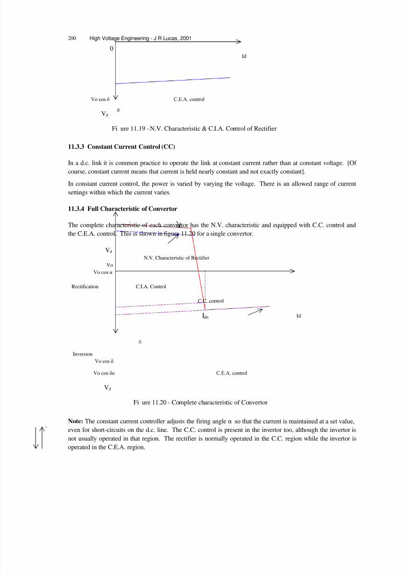
8/6/2019 High Voltage Engineering (Lucas)
http://slidepdf.com/reader/full/high-voltage-engineering-lucas 208/212
High Voltage Engineering - J R Lucas, 2001200
11.3.3 Constant Current Control (CC)
In a d.c. link it is common practice to operate the link at constant current rather than at constant voltage. [Of course, constant current means that current is held nearly constant and not exactly constant].
In constant current control, the power is varied by varying the voltage. There is an allowed range of currentsettings within which the current varies.
11.3.4 Full Characteristic of Convertor
The complete characteristic of each convertor has the N.V. characteristic and equipped with C.C. control andthe C.E.A. control. This is shown in figure 11.20 for a single convertor.
Note: The constant current controller adjusts the firing angle . VR WKDW WKH FXUUHQW LV PDLQWDLQHGeven for short-circuits on the d.c. line. The C.C. control is present in the invertor too, although the invertor isnot usually operated in that region. The rectifier is normally operated in the C.C. region while the invertor isoperated in the C.E.A. region.
0Id
9R FRV/ & ( $ FRQWURO
Vd
Fi ure 11.19 - N.V. Characteristic & C.I.A. Control of Rectifier
Vd N.V. Characteristic of Rectifier
Vo9R FRV.
Rectification C.I.A. Control
C.C. control
Ids Id
Inversion9R FRV/
9R FRV/R & ( $ FRQWU
Vd
Fi ure 11.20 - Complete characteristic of Convertor

8/6/2019 High Voltage Engineering (Lucas)
http://slidepdf.com/reader/full/high-voltage-engineering-lucas 209/212
High Voltage Direct Current Transmission 201
11.3.5 Compounding of Convertors
Figure 11.21 shows a system of 2 convertors, connected by a hvdc link. Both convertors are provided withCEA and CC control so that either can work as a rectifier or an invertor. The compounded characteristics areshown in figure 11.22.
The margin setting I dm between the current setting I ds for the invertor and for the rectifier is usually kept atabout 10% to 20% of the current setting. The setting of the convertor operating as rectifier is kept higher thanthe setting of that as invertor by the margin setting I dm.
The usual operating point for power transfer is the intersection of the CC control of the rectifier and the CEAcontrol of the invertor. (For comparison, the characteristics of convertor B has been drawn inverted). It must
also be ensured by proper tap changing that the N.V. characteristic of the convertor operating in therectification mode is higher than the C.E.A. characteristic of the invertor, as V o of the two ends are notnecessarily equal.
Figure 11.21 - Compounding of Convertors
Fi ure 11.22 - Compounded characteristic of Convertors
∧ ∧
∨ ∨
C.E.A.Control
PhaseAdvance
Circuit
C.C.Control
Control for
Convertor B
Control forConvertor A
hvdc link convertor Bconvertor A3-phase ac
Id
Id
IdmIds
E
Vd
A as RectifierB as Invertor
A as InvertorB as Rectifier
N.V. Characteristic of A
N.V. Characteristic of B
C.E.A. control of A
C.E.A. control of B
C.C. control of A(A as rectifier)
changedC.C. control of Afor A as invertor
Vo
Vo cos δ
Vo
Vo cos δ
Vd
Ids+Idm
Ids
Ids−Idm
8/6/2019 High Voltage Engineering (Lucas)
http://slidepdf.com/reader/full/high-voltage-engineering-lucas 210/212
High Voltage Engineering - J R Lucas, 2001202
With convertor A operating as rectifier, and convertor B operating as invertor, the steady state current under allcircumstances will remain within the upper limit (I ds + Idm) and the lower limit I ds. That is, the system directcurrent will not change by more than I dm under all operating conditions. By reversing the margin setting I dm,that is making the setting of convertor B to exceed that of A, power flow can be automatically reversed.Convertor B will then operate as a rectifier and A as an invertor. The reversal of power occurs as a result of the
reversal of polarity of the voltage.
11.3.6 Per Unit Convertor Chart
The convertor operating equations for voltage V d and current I d are expressed as follows.
It is useful to draw the convertor chart in per unit. For this purpose the natural selection for the base voltage isthe maximum direct voltage output V do. There is no such natural current base. Thus it is convenient to selectthe constant appearing in equation (11.5) for current as the base quantity. Thus the selected base quantities areas given in equation (11.15).
2)w+(
E 23
=V d coscos α
π
)w-( L2
E = I
cd coscos α
ω
Figure 11.23 - Per unit convertor chart
Vd
Id
1.0
0.5
0
-0.5
-1.0
0.5 1.0
w =15 o
w =30 o
w =45 o
w =60 o
w =75 o
w =90 o
w =105 o
w =120 o
w =135 o
w =150 o
w =165 o
w =180 o
α =15 o
w =0 o
α =0 o α =30 oα =45o
α =60 o
α =75 o
γ =15 oγ =30 o
γ =45 o
γ =60 oα =90 o
α =105 o
α =120 o
α =135 o
α =150 o
α =180 o
α =165 o

8/6/2019 High Voltage Engineering (Lucas)
http://slidepdf.com/reader/full/high-voltage-engineering-lucas 211/212
High Voltage Direct Current Transmission 203
With these base quantities, the per unit voltage Vd and per unit current Id are given as follows.
Vd = ½ ( cos . FRV Z DQGId = cos . - cos w
which give the simple per unit characteristic equations (11.16) and (11.17).
Vd + 0.5 Id = cos . (11.16)
Vd - 0.5 Id = cos w (11.17)
In the chosen per unit system, constant delay angle control (or the natural voltage characteristic) correspond tostraight lines with slope (-) 0.5 on the per unit voltage-current chart. Similarly constant extinction angle control
correspond to straight lines with slope (+) 0.5.
For inversion, the corresponding equations are as follows.
Vd + 0.5 Id = cos ( - - FRV Vd - 0.5 Id = cos ( - / - FRV/
Since voltages are measured in the opposite direction for inversion, these equations may be rewritten in theirmore usual form as in equations (11.18) and (11.19).
(-) V d - 0.5 Id = cos (11.18)(-) Vd + 0.5 Id = cos / (11.19)
From the characteristics, the constant commutation angle characteristic may be obtained by subtraction asfollows.
- / RU Z- .
The constant FKDUDFWHULVWLFV FDQ EH VKRZQ WR EH HOOLSVHV0). The per unit operating chart of theconvertor is shown in figure 11.23.
11.4 Classification of d.c. links
D.C. links are classified into Monopolar links, Bipolar links, and Homopolar links.
In the case of the monopolar link there is only one conductor and the ground serves as the return path. The link normally operates at negative polarity as there is less corona loss and radio interference is reduced. Figure11.23 (a) shows a monopolar link.
The bipolar links have two conductors, one operating at positive polarity and the other operating at negativepolarity. The junction between the two convertors may be grounded at one or both ends. The ground does notnormally carry a current. However, if both ends are grounded, each link could be independently operated when
necessary. This is shown in figure 11.23 (b).
L2
E = I ,
E 23 =V
cbasebase
ω π (11.15)
8/6/2019 High Voltage Engineering (Lucas)
http://slidepdf.com/reader/full/high-voltage-engineering-lucas 212/212
High Voltage Engineering - J R Lucas, 2001204
(a) monopolar link
∨ ∨
∧ ∧
∨ ∨
∧ ∧
∨ ∨
∧ ∧