highly integrated resonant tunneling diode with
TRANSCRIPT

electronics
Article
Highly Integrated Resonant Tunneling Diode withRectangular Waveguide Output for W-BandCommunication System
Caixia Wang 1 , Yuan Yao 1,*, Hang Jiang 1, Tao Xiu 1, Mohsin A. Shah Syedd 1, Junsheng Yu 1
and Xiaodong Chen 2
1 School of Electronic Engineering, Beijing University of Posts and Telecommunications, Beijing 100876, China;[email protected] (C.W); [email protected] (H.J.); [email protected] (T.X.);[email protected] (M.A.S.S.); [email protected] (J.Y.)
2 School of Electronic Engineering and Computer Science, Queen Mary, University of London,London E1 4NS, UK; [email protected]
* Correspondence: [email protected]
Received: 12 February 2020; Accepted: 13 March 2020; Published: 15 March 2020
Abstract: A packaged resonant tunneling diode (RTD) with rectangular waveguide output forhighly integrated wireless communication is proposed. The output signal of the RTD chip isradiated to the rectangular waveguide through an E plane probe transformer. Next, the RTD chip iselectrically connected to the transformer by using gold wire bonding. The packaged RTD exhibits anoscillation frequency of 92 GHz, while the maximum radio frequency (RF) output power is −7 dBm.A miniaturized and high data rate wireless communication system with a 7 Gbps on–off keying(OOK) module by using the RTD is demonstrated, and the bit error rate (BER) of the 7 Gbps is below3.8 × 10−3.
Keywords: resonant tunneling diode; rectangular waveguide; highly integration; W band;wireless communication
1. Introduction
There has been an explosive growth of data capacity and data rate in fifth generation wirelessnetworks (5G) [1]. The millimeter wave and terahertz frequency range has a large amount of unlicensedspectra, and this has gotten a lot of attention in wireless communication [2,3].
The millimeter wave and terahertz communication systems mainly include all-electronic andoptoelectronic systems. The advantage of all-electronics systems is higher output power, but their datarate is lower [4,5]. Most of the optoelectronic systems are based on uni-traveling carrier photodiode(UTC-PD), which can obtain a higher data rate [6,7]. However, its system integration is poor due to itscomplicated optical equipment.
A resonant tunneling diode (RTD) is a high speed solid-state device [8]. Recently, many literatureson short distance and high data rate wireless communication with RTD have been published [9–13].In [9], wireless data transmission by direct amplitude shift keying was demonstrated by using an RTDoscillating at 542 GHz, with a data rate of 3 Gbps. In [10], a 9 Gbps on–off keying module system wasachieved, and the RTDs awee employed to be the transmitter and receiver by changing the bias voltageof the RTD. In [11], a wireless data transmission of 34 Gbit/s at 500 GHz range was proposed, where theoutput power was about 60 µW. To improve the RF output power, J. Park et al. designed an RTD pairconfiguration to obtain an increased negative differential conductance voltage span; the maximumRF output power was −1.76 dBm at 24.1 GHz [12]. In the same year, J. Wang et al. also proposed an
Electronics 2020, 9, 485; doi:10.3390/electronics9030485 www.mdpi.com/journal/electronics

Electronics 2020, 9, 485 2 of 10
improved RTD pair, and the maximum output power was 2 mW without any power amplifier at theoscillator frequency 84 GHz [13].
However, the use of a probe station and DC bias lines reduce the flexibility of RTD chips, and theexposed RTD chips are susceptible to mechanical damage, which makes them difficult to apply inthe communication system. In addition, to the best of our knowledge, there has been no literatureon a packaged RTD due to the complicated packaged process, including DC bias, electrical signalconnection, and efficient RF conversion.
Most millimeter wave and terahertz devices are waveguide output. To enhance system integrity,it is necessary to package the RTD with a rectangular waveguide output. In this paper, an RTD withrectangular waveguide output for a W band communication system application is presented. First,a coplanar waveguide (CPW) transition to rectangular waveguide structure based on the E plane probewas designed to achieve the output signal of the RTD efficiently coupled into rectangular waveguide.Then, we designed the packaged RTD structure, and we fabricated and measured the performanceof the packaged RTD. Measured results demonstrated that the oscillation frequency of the packagedRTD was from 88 to 92 GHz, and the maximum RF output power was −7 dBm. Finally, to verify thewireless transmission capability of the packaged RTD, a highly integrated and high speed wirelesscommunication system based on on–off keying (OOK) modulation with the RTD was built, and thedate rate of 7 Gbps was realized.
2. CPW—Waveguide Transformer Design
2.1. Transformer Structure Design
Figure 1 shows the structure of CPW transition to waveguide. The rectangular waveguide was astandard WR-10 waveguide, and a window connecting to the air cavity was opened in parallel with the Hplane of the waveguide. The length of the window was the same as the CPW length, and the width andheight of the window were ws and la, respectively. One end of the rectangular waveguide was blockedwith solid metal block. An H plane bend structure was designed to facilitate the measure, and the bendingradii were r1 and r2, as shown in Figure 1c. The fan-shaped radiation part connected to the end of the signaltrace of the CPW was used to propagate the wave of the CPW into the waveguide, as shown in Figure 2.The E plane probe was designed on the high permittivity Al2O3 substrate. The relative permittivity was9.8, and the height was 127 µm. The numerical analysis software Ansoft HFSS (High Frequency StructureSimulator) was used to simulate the configuration. The red parts in the Figure 1a are the wave ports,and the optimized detailed parameters of the transformer are shown in Table 1.
Electronics 2020, 9, x FOR PEER REVIEW 3 of 10
z
x y
WR10
a
bPort 1
Port 2
la
ws
d
z
x yh
(a) (b) WR-10
WR-10r1
r2 (c)
Figure 1. The configuration of the transformer. (a) 3D view; (b) side view; and (c) H plane bend.
z
xy
B ls
ws wgrs
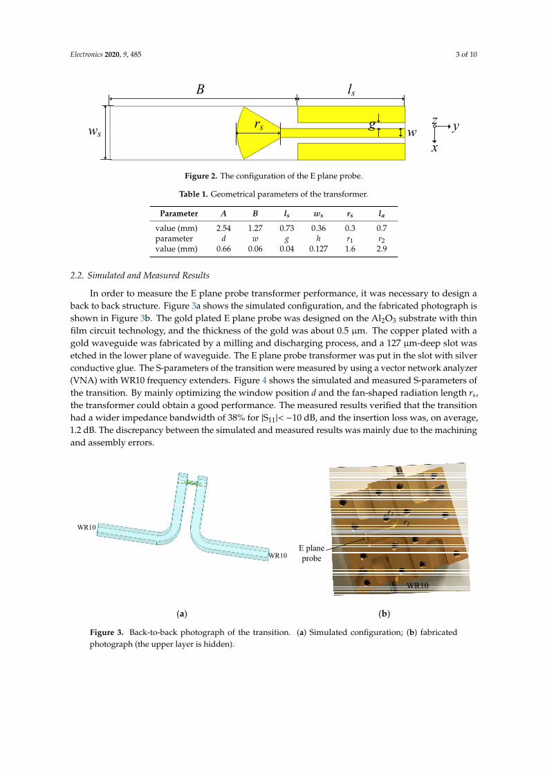
Figure 2. The configuration of the E plane probe.
Table 1. Geometrical parameters of the transformer.
Parameter A B ls ws rs la
value (mm) 2.54 1.27 0.73 0.36 0.3 0.7
parameter d w g h r1 r2
value (mm) 0.66 0.06 0.04 0.127 1.6 2.9
2.2. Simulated and Measured Results
In order to measure the E plane probe transformer performance, it was necessary to design a back to back structure. Figure 3a shows the simulated configuration, and the fabricated photograph is shown in Figure 3b. The gold plated E plane probe was designed on the Al2O3 substrate with thin film circuit technology, and the thickness of the gold was about 0.5 μm. The copper plated with a gold waveguide was fabricated by a milling and discharging process, and a 127 μm-deep slot was etched in the lower plane of waveguide. The E plane probe transformer was put in the slot with silver conductive glue. The S-parameters of the transition were measured by using a vector network analyzer (VNA) with WR10 frequency extenders. Figure 4 shows the simulated and measured S-parameters of the transition. By mainly optimizing the window position d and the fan-shaped radiation length rs, the transformer could obtain a good performance. The measured results verified that the transition had a wider impedance bandwidth of 38% for |S11|< −10 dB, and the insertion loss was, on average, 1.2 dB. The discrepancy between the simulated and measured results was mainly due to the machining and assembly errors.
Figure 1. The configuration of the transformer. (a) 3D view; (b) side view; and (c) H plane bend.
Electronics 2020, 9, 485 3 of 10
Electronics 2020, 9, x FOR PEER REVIEW 3 of 10
z
x y
WR10
a
bPort 1
Port 2
la
ws
d
z
x yh
(a) (b) WR-10
WR-10r1
r2 (c)
Figure 1. The configuration of the transformer. (a) 3D view; (b) side view; and (c) H plane bend.
z
xy
B ls
ws wgrs
Figure 2. The configuration of the E plane probe.
Table 1. Geometrical parameters of the transformer.
Parameter A B ls ws rs la
value (mm) 2.54 1.27 0.73 0.36 0.3 0.7
parameter d w g h r1 r2
value (mm) 0.66 0.06 0.04 0.127 1.6 2.9
2.2. Simulated and Measured Results
In order to measure the E plane probe transformer performance, it was necessary to design a back to back structure. Figure 3a shows the simulated configuration, and the fabricated photograph is shown in Figure 3b. The gold plated E plane probe was designed on the Al2O3 substrate with thin film circuit technology, and the thickness of the gold was about 0.5 μm. The copper plated with a gold waveguide was fabricated by a milling and discharging process, and a 127 μm-deep slot was etched in the lower plane of waveguide. The E plane probe transformer was put in the slot with silver conductive glue. The S-parameters of the transition were measured by using a vector network analyzer (VNA) with WR10 frequency extenders. Figure 4 shows the simulated and measured S-parameters of the transition. By mainly optimizing the window position d and the fan-shaped radiation length rs, the transformer could obtain a good performance. The measured results verified that the transition had a wider impedance bandwidth of 38% for |S11|< −10 dB, and the insertion loss was, on average, 1.2 dB. The discrepancy between the simulated and measured results was mainly due to the machining and assembly errors.
Figure 2. The configuration of the E plane probe.
Table 1. Geometrical parameters of the transformer.
Parameter A B ls ws rs la
value (mm) 2.54 1.27 0.73 0.36 0.3 0.7parameter d w g h r1 r2value (mm) 0.66 0.06 0.04 0.127 1.6 2.9
2.2. Simulated and Measured Results
In order to measure the E plane probe transformer performance, it was necessary to design aback to back structure. Figure 3a shows the simulated configuration, and the fabricated photograph isshown in Figure 3b. The gold plated E plane probe was designed on the Al2O3 substrate with thinfilm circuit technology, and the thickness of the gold was about 0.5 µm. The copper plated with agold waveguide was fabricated by a milling and discharging process, and a 127 µm-deep slot wasetched in the lower plane of waveguide. The E plane probe transformer was put in the slot with silverconductive glue. The S-parameters of the transition were measured by using a vector network analyzer(VNA) with WR10 frequency extenders. Figure 4 shows the simulated and measured S-parameters ofthe transition. By mainly optimizing the window position d and the fan-shaped radiation length rs,the transformer could obtain a good performance. The measured results verified that the transitionhad a wider impedance bandwidth of 38% for |S11|< −10 dB, and the insertion loss was, on average,1.2 dB. The discrepancy between the simulated and measured results was mainly due to the machiningand assembly errors.Electronics 2020, 9, x FOR PEER REVIEW 4 of 10
WR10
WR10
E plane probe
WR10
r1r2
(a) (b)
Figure 3. Back-to-back photograph of the transition. (a) Simulated configuration; (b) fabricated photograph (the upper layer is hidden).
75 80 85 90 95 100 105 110-45
-40
-35
-30
-25
-20
-15
-10
-5
0
S 21 (d
B)
S 11 (d
B)
Frequency (GHz)
Sim. Mea.
-14
-12
-10
-8
-6
-4
-2
0
Figure 4. Simulated and measured S-parameters of the transition.
3. Package and Measurement of RTD
The packaged RTD configuration with WR10 waveguide output and an SMA connector is shown in Figure 5. The packaged RTD consisted of a DC bias microstrip line (MSL), an RTD chip, an E plane probe transformer, and a metallic cavity with WR 10 waveguide output. The DC bias MSL that was connected to an SMA connector was used to bias the RTD. The MSL was designed on the Rogers 6010 substrate with a relative permittivity of 10.2 and a thickness of 127 μm. The width of the MSL was 0.1 mm to match with the 50 Ω SMA connector. The RTD chip was the same as in the one used in the literature [14], and the indium phosphide (InP) substrate height of the RTD was 600 μm. The E plane probe transformer was used to radiate the RF signal of the RTD to the WR 10 waveguide. By using gold wire bonding, the signal and ground traces of the RTD were connected to the E plane probe transformer and the DC MSL was bonded to the DC trace of the RTD. A metallic package cavity with a WR-10 standard waveguide output was fabricated. We etched three slots in the cavity and used a conductive silver glue to fix the transformer, the RTD chip, and the DC bias MSL inside the cavity. The photograph and micrograph of the fabricated packaged RTD is shown in Figure 6.
Figure 3. Back-to-back photograph of the transition. (a) Simulated configuration; (b) fabricatedphotograph (the upper layer is hidden).

Electronics 2020, 9, 485 4 of 10
Electronics 2020, 9, x FOR PEER REVIEW 4 of 10
WR10
WR10
E plane probe
WR10
r1r2
(a) (b)
Figure 3. Back-to-back photograph of the transition. (a) Simulated configuration; (b) fabricated photograph (the upper layer is hidden).
75 80 85 90 95 100 105 110-45
-40
-35
-30
-25
-20
-15
-10
-5
0
S 21 (d
B)
S 11 (d
B)
Frequency (GHz)
Sim. Mea.
-14
-12
-10
-8
-6
-4
-2
0
Figure 4. Simulated and measured S-parameters of the transition.
3. Package and Measurement of RTD
The packaged RTD configuration with WR10 waveguide output and an SMA connector is shown in Figure 5. The packaged RTD consisted of a DC bias microstrip line (MSL), an RTD chip, an E plane probe transformer, and a metallic cavity with WR 10 waveguide output. The DC bias MSL that was connected to an SMA connector was used to bias the RTD. The MSL was designed on the Rogers 6010 substrate with a relative permittivity of 10.2 and a thickness of 127 μm. The width of the MSL was 0.1 mm to match with the 50 Ω SMA connector. The RTD chip was the same as in the one used in the literature [14], and the indium phosphide (InP) substrate height of the RTD was 600 μm. The E plane probe transformer was used to radiate the RF signal of the RTD to the WR 10 waveguide. By using gold wire bonding, the signal and ground traces of the RTD were connected to the E plane probe transformer and the DC MSL was bonded to the DC trace of the RTD. A metallic package cavity with a WR-10 standard waveguide output was fabricated. We etched three slots in the cavity and used a conductive silver glue to fix the transformer, the RTD chip, and the DC bias MSL inside the cavity. The photograph and micrograph of the fabricated packaged RTD is shown in Figure 6.
Figure 4. Simulated and measured S-parameters of the transition.
3. Package and Measurement of RTD
The packaged RTD configuration with WR10 waveguide output and an SMA connector is shownin Figure 5. The packaged RTD consisted of a DC bias microstrip line (MSL), an RTD chip, an E planeprobe transformer, and a metallic cavity with WR 10 waveguide output. The DC bias MSL that wasconnected to an SMA connector was used to bias the RTD. The MSL was designed on the Rogers 6010substrate with a relative permittivity of 10.2 and a thickness of 127 µm. The width of the MSL was0.1 mm to match with the 50 Ω SMA connector. The RTD chip was the same as in the one used in theliterature [14], and the indium phosphide (InP) substrate height of the RTD was 600 µm. The E planeprobe transformer was used to radiate the RF signal of the RTD to the WR 10 waveguide. By usinggold wire bonding, the signal and ground traces of the RTD were connected to the E plane probetransformer and the DC MSL was bonded to the DC trace of the RTD. A metallic package cavity witha WR-10 standard waveguide output was fabricated. We etched three slots in the cavity and used aconductive silver glue to fix the transformer, the RTD chip, and the DC bias MSL inside the cavity.The photograph and micrograph of the fabricated packaged RTD is shown in Figure 6.
Figure 7 shows the I–V characteristics of the packaged RTD. The RTD chip in the literature [14]consists of two RTDs that are connected in parallel, and each device is biased individually with resistorRe. Because of the additional current through the shunt resistor that is connected in parallel with theRTD, a negative differential resistance (NDR) region was not observed in the I–V curve [13]. Instead,a small decline of 1.05 V was observed, and 1.05 V was the bias point of the RTD. As proposed in [14],by changing the DC voltage, an RTD can operate in negative differential resistance region or positiveresistance region. Therefore, an RTD can be biased to switch between the on and off states withOOK modulation. The voltage-dependent frequency and output power of RTD is shown in Figure 8.The oscillator frequency ranged from 88 to 92 GHz, and the maximum RF output power was −8.6 dBm.When the losses of the cable, the SMA adapters, and the bias-T were removed, the actual output powerwas at least −7 dBm. Figure 9 shows the output spectrum at 90 GHz when DC = 1.2 V.
The carrier frequency of the RTD with a waveguide output increased by 15 GHz compared withthe RTD chip, an effect that was mainly caused by gold wire bonding. The packaged RTD equivalentcircuit, including gold wire bonding, is shown in Figure 10. The RTD oscillator circuit part was thesame as [15], and −G1n and −G2n were the negative differential conductances of RTD1 and RTD2,respectively, while C1n and C2n were the self-capacitances of each RTD. The gold wire was equivalentto series inductance and parallel capacitance. Generally, the effect of shunt capacitors is negligible dueto their smaller value. Oscillator frequency can be determined by equating the admittance imaginarypart to zero, as shown in Equation (1):

Electronics 2020, 9, 485 5 of 10
f =1
2π
√(C1n + C1n)
LLgL+Lg
(1)
where Lg is the series inductance of gold wire. It can be seen that the total inductance in the circuit wasdecreased compared with that of [15], which led to the increased carrier frequency.Electronics 2020, 9, x FOR PEER REVIEW 5 of 10
SMA
DC bias MSL
RTD
RFDC
E plane probe
transformer
Waveguide
Gold wire
Metallic cavity
(a) Top view
RogersInP
Al2O3600 um
127 um 127 um
DC
Waveguide
RF
Metallic cavity
RF
(b) Side view
Figure 5. The packaged resonant tunneling diode (RTD) configuration.
E plane probe
RTD
DC
Microstrip line
Figure 6. Photograph and micrograph of the RTD with a rectangular waveguide output.
Figure 7 shows the I–V characteristics of the packaged RTD. The RTD chip in the literature [14]
consists of two RTDs that are connected in parallel, and each device is biased individually with
resistor Re. Because of the additional current through the shunt resistor that is connected in parallel
with the RTD, a negative differential resistance (NDR) region was not observed in the I–V curve [13].
Instead, a small decline of 1.05 V was observed, and 1.05 V was the bias point of the RTD. As proposed
in [14], by changing the DC voltage, an RTD can operate in negative differential resistance region or
positive resistance region. Therefore, an RTD can be biased to switch between the on and off states
with OOK modulation. The voltage-dependent frequency and output power of RTD is shown in
Figure 8. The oscillator frequency ranged from 88 to 92 GHz, and the maximum RF output power
was −8.6 dBm. When the losses of the cable, the SMA adapters, and the bias-T were removed, the
actual output power was at least −7 dBm. Figure 9 shows the output spectrum at 90 GHz when DC =
1.2 V.
Figure 5. The packaged resonant tunneling diode (RTD) configuration.
Electronics 2020, 9, x FOR PEER REVIEW 5 of 10
SMA
DC bias MSL
RTD
RFDC
E plane probe transformer
Waveguide
Gold wire
Metallic cavity
(a) Top view
Rogers InP Al2O3600 um127 um 127 um
DC
Waveguide
RF
Metallic cavity
RF
(b) Side view
Figure 5. The packaged resonant tunneling diode (RTD) configuration.
E plane probe
RTD
DC Microstrip line
Figure 6. Photograph and micrograph of the RTD with a rectangular waveguide output.
Figure 7 shows the I–V characteristics of the packaged RTD. The RTD chip in the literature [14] consists of two RTDs that are connected in parallel, and each device is biased individually with resistor Re. Because of the additional current through the shunt resistor that is connected in parallel with the RTD, a negative differential resistance (NDR) region was not observed in the I–V curve [13]. Instead, a small decline of 1.05 V was observed, and 1.05 V was the bias point of the RTD. As proposed in [14], by changing the DC voltage, an RTD can operate in negative differential resistance region or positive resistance region. Therefore, an RTD can be biased to switch between the on and off states with OOK modulation. The voltage-dependent frequency and output power of RTD is shown in Figure 8. The oscillator frequency ranged from 88 to 92 GHz, and the maximum RF output power was −8.6 dBm. When the losses of the cable, the SMA adapters, and the bias-T were removed, the actual output power was at least −7 dBm. Figure 9 shows the output spectrum at 90 GHz when DC = 1.2 V.
Figure 6. Photograph and micrograph of the RTD with a rectangular waveguide output.

Electronics 2020, 9, 485 6 of 10Electronics 2020, 9, x FOR PEER REVIEW 6 of 10
bias point
0.0 0.2 0.4 0.6 0.8 1.0 1.20
20
40
60
80
100
120
Curre
nt (m
A)
Voltage (V)
00
10
1
NRZ-input
Figure 7. The I–V characteristics of the packaged RTD.
1.05 1.10 1.15 1.20 1.25 1.30
84
86
88
90
92
94
Pow
er (d
Bm)
Freq
(GH
z)
Voltage (V)
Freq
-9.6
-9.2
-8.8
-8.4
-8.0
Power
Figure 8. Measured voltage-dependent frequency and output power of the RTD.
Figure 7. The I–V characteristics of the packaged RTD.
Electronics 2020, 9, x FOR PEER REVIEW 6 of 10
bias point
0.0 0.2 0.4 0.6 0.8 1.0 1.20
20
40
60
80
100
120
Curre
nt (m
A)
Voltage (V)
00
10
1
NRZ-input
Figure 7. The I–V characteristics of the packaged RTD.
1.05 1.10 1.15 1.20 1.25 1.30
84
86
88
90
92
94
Pow
er (d
Bm)
Freq
(GH
z)
Voltage (V)
Freq
-9.6
-9.2
-8.8
-8.4
-8.0
Power
Figure 8. Measured voltage-dependent frequency and output power of the RTD. Figure 8. Measured voltage-dependent frequency and output power of the RTD.Electronics 2020, 9, x FOR PEER REVIEW 7 of 10
89.0 89.2 89.4 89.6 89.8 90.0 90.2 90.4 90.6 90.8 91.0-80
-70
-60
-50
-40
-30
-20
-10
0
Am
plitu
de (d
Bm)
Frequency (GHz) Figure 9. Measured output spectrum of the RTD oscillator.
The carrier frequency of the RTD with a waveguide output increased by 15 GHz compared with the RTD chip, an effect that was mainly caused by gold wire bonding. The packaged RTD equivalent circuit, including gold wire bonding, is shown in Figure 10. The RTD oscillator circuit part was the same as [15], and −G1n and −G2n were the negative differential conductances of RTD1 and RTD2, respectively, while C1n and C2n were the self-capacitances of each RTD. The gold wire was equivalent to series inductance and parallel capacitance. Generally, the effect of shunt capacitors is negligible due to their smaller value. Oscillator frequency can be determined by equating the admittance imaginary part to zero, as shown in Equation (1):
1
2 ( )1 1
fLLg
C Cn nL Lg
π
=
++
(1)
where Lg is the series inductance of gold wire. It can be seen that the total inductance in the circuit was decreased compared with that of [15], which led to the increased carrier frequency.
Figure 11 shows the output spectrum with OOK modulation at 90 GHz when DC = 1.2 V. The modulation signal was a pseudorandom bit sequence (PRBS) with repetition length 215–1, and the data rate was 4 Gbps. The first null appeared at 94 GHz, which verified the feasibility of the packaged RTD for OOK modulation.
L -G1n C1n -G2n C2n RL Cg Cg
Rg LgRTD1 RTD2
Bonding wire
Figure 10. Packaged RTD equivalent circuit including gold wire bonding.
Figure 9. Measured output spectrum of the RTD oscillator.

Electronics 2020, 9, 485 7 of 10
Figure 11 shows the output spectrum with OOK modulation at 90 GHz when DC = 1.2 V.The modulation signal was a pseudorandom bit sequence (PRBS) with repetition length 215–1, and thedata rate was 4 Gbps. The first null appeared at 94 GHz, which verified the feasibility of the packagedRTD for OOK modulation.
Electronics 2020, 9, x FOR PEER REVIEW 7 of 10
89.0 89.2 89.4 89.6 89.8 90.0 90.2 90.4 90.6 90.8 91.0-80
-70
-60
-50
-40
-30
-20
-10
0
Am
plitu
de (d
Bm)
Frequency (GHz) Figure 9. Measured output spectrum of the RTD oscillator.
The carrier frequency of the RTD with a waveguide output increased by 15 GHz compared with the RTD chip, an effect that was mainly caused by gold wire bonding. The packaged RTD equivalent circuit, including gold wire bonding, is shown in Figure 10. The RTD oscillator circuit part was the same as [15], and −G1n and −G2n were the negative differential conductances of RTD1 and RTD2, respectively, while C1n and C2n were the self-capacitances of each RTD. The gold wire was equivalent to series inductance and parallel capacitance. Generally, the effect of shunt capacitors is negligible due to their smaller value. Oscillator frequency can be determined by equating the admittance imaginary part to zero, as shown in Equation (1):
1
2 ( )1 1
fLLg
C Cn nL Lg
π
=
++
(1)
where Lg is the series inductance of gold wire. It can be seen that the total inductance in the circuit was decreased compared with that of [15], which led to the increased carrier frequency.
Figure 11 shows the output spectrum with OOK modulation at 90 GHz when DC = 1.2 V. The modulation signal was a pseudorandom bit sequence (PRBS) with repetition length 215–1, and the data rate was 4 Gbps. The first null appeared at 94 GHz, which verified the feasibility of the packaged RTD for OOK modulation.
L -G1n C1n -G2n C2n RL Cg Cg
Rg LgRTD1 RTD2
Bonding wire
Figure 10. Packaged RTD equivalent circuit including gold wire bonding. Figure 10. Packaged RTD equivalent circuit including gold wire bonding.Electronics 2020, 9, x FOR PEER REVIEW 8 of 10
80 85 90 95 100-80
-70
-60
-50
-40
-30
-20
-10
0
Am
plitu
de (d
Bm)
Frequency (GHz)
4Gbps4Gbps
m1 m1Frequency = 90 GHz
Amplitude = -9 dBm
Figure 11. Measured output spectrum of RTD with OOK modulation.
4. System Demonstration
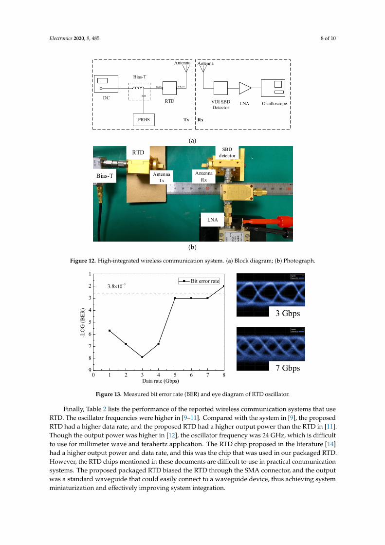
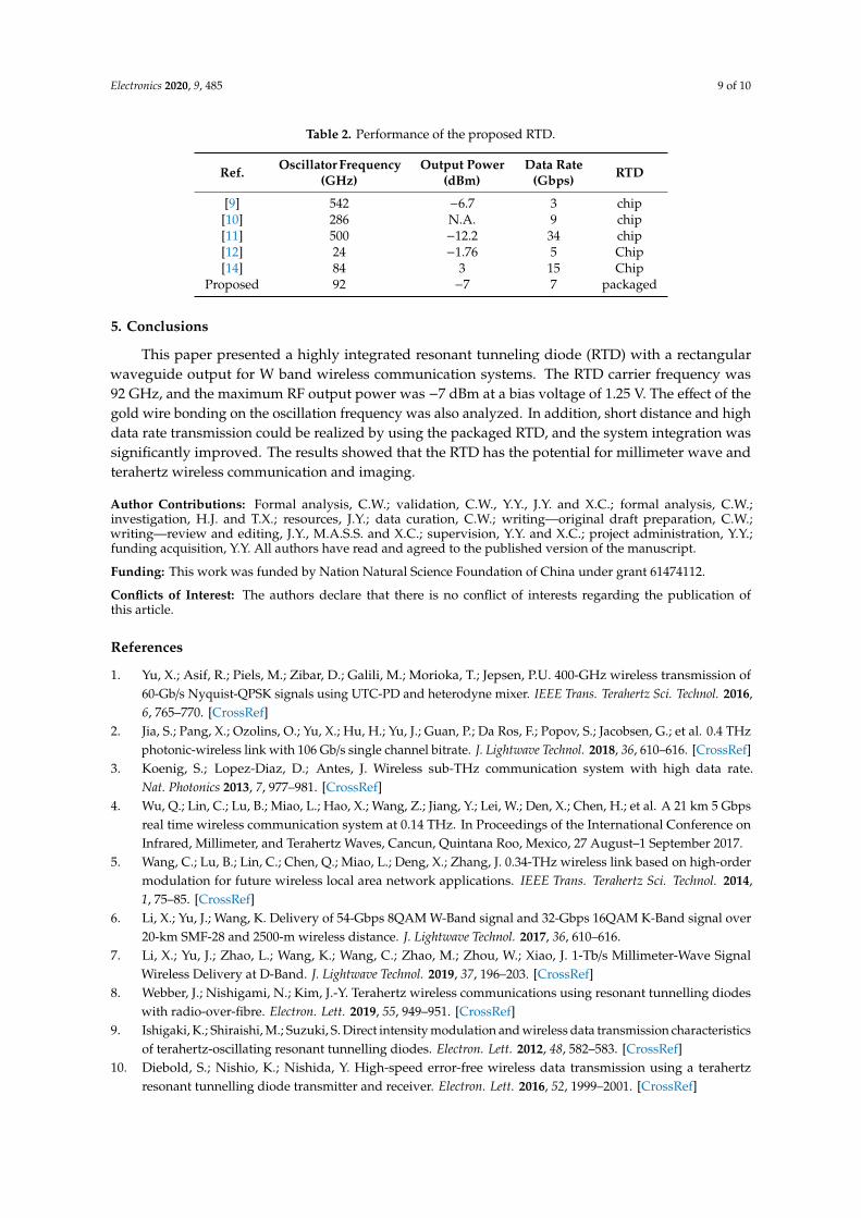
The highly integrated wireless communication system is shown in Figure 12. The RTD was the transmitter, and bias-T was used for applying DC and PRBS signals to the RTD. Two waveguide antennas with a gain of 10 dBic were employed to transmit and receive signals. The data were demodulated by a zero bias VDI SBD detector, and then they were amplified by a low noise amplifier (LNA). The bias voltage was 1.2 V instead of 1.05 V due to the loss of the bias-T, and the amplitude of PRBS signal ranged from −100 to 100 mV. It can be seen from Figure 7 that 1.05 + 0.1 V was in the NDR (on state), while 1.05 − 0.1 V was in the positive resistance region (off state). The transmission distance was 5 cm, and the maximum data rate was 8 Gbps. The bit error rate and eye diagram are shown in Figure 13. The BER was below 3.8 × 10⁻³ up to 7 Gbps.
DC
Bias-T
RTD VDI SBDDetector
LNA
WR-10SMA
Oscilloscope
PRBS Tx
Antenna Antenna
Rx
(a)
Bias-T
RTD
Antenna Tx
Antenna Rx
SBD detector
LNA
(b)
Figure 12. High-integrated wireless communication system. (a) Block diagram; (b) Photograph.
Figure 11. Measured output spectrum of RTD with OOK modulation.
4. System Demonstration
The highly integrated wireless communication system is shown in Figure 12. The RTD was thetransmitter, and bias-T was used for applying DC and PRBS signals to the RTD. Two waveguideantennas with a gain of 10 dBic were employed to transmit and receive signals. The data weredemodulated by a zero bias VDI SBD detector, and then they were amplified by a low noise amplifier(LNA). The bias voltage was 1.2 V instead of 1.05 V due to the loss of the bias-T, and the amplitude ofPRBS signal ranged from −100 to 100 mV. It can be seen from Figure 7 that 1.05 + 0.1 V was in the NDR(on state), while 1.05 − 0.1 V was in the positive resistance region (off state). The transmission distancewas 5 cm, and the maximum data rate was 8 Gbps. The bit error rate and eye diagram are shown inFigure 13. The BER was below 3.8 × 10⁻³ up to 7 Gbps.
Electronics 2020, 9, 485 8 of 10
Electronics 2020, 9, x FOR PEER REVIEW 8 of 10
80 85 90 95 100-80
-70
-60
-50
-40
-30
-20
-10
0
Am
plitu
de (d
Bm)
Frequency (GHz)
4Gbps4Gbps
m1 m1Frequency = 90 GHz
Amplitude = -9 dBm
Figure 11. Measured output spectrum of RTD with OOK modulation.
4. System Demonstration
The highly integrated wireless communication system is shown in Figure 12. The RTD was the transmitter, and bias-T was used for applying DC and PRBS signals to the RTD. Two waveguide antennas with a gain of 10 dBic were employed to transmit and receive signals. The data were demodulated by a zero bias VDI SBD detector, and then they were amplified by a low noise amplifier (LNA). The bias voltage was 1.2 V instead of 1.05 V due to the loss of the bias-T, and the amplitude of PRBS signal ranged from −100 to 100 mV. It can be seen from Figure 7 that 1.05 + 0.1 V was in the NDR (on state), while 1.05 − 0.1 V was in the positive resistance region (off state). The transmission distance was 5 cm, and the maximum data rate was 8 Gbps. The bit error rate and eye diagram are shown in Figure 13. The BER was below 3.8 × 10⁻³ up to 7 Gbps.
DC
Bias-T
RTD VDI SBDDetector
LNA
WR-10SMA
Oscilloscope
PRBS Tx
Antenna Antenna
Rx
(a)
Bias-T
RTD
Antenna Tx
Antenna Rx
SBD detector
LNA
(b)
Figure 12. High-integrated wireless communication system. (a) Block diagram; (b) Photograph. Figure 12. High-integrated wireless communication system. (a) Block diagram; (b) Photograph.Electronics 2020, 9, x FOR PEER REVIEW 9 of 10
0 1 2 3 4 5 6 7 89
8
7
6
5
4
3
2
1
3.8×10⁻³
-LO
G (B
ER)
Data rate (Gbps)
Bit error rate
3 Gbps
7 Gbps
Figure 13. Measured bit error rate (BER) and eye diagram of RTD oscillator.
Finally, Table 2 lists the performance of the reported wireless communication systems that use RTD. The oscillator frequencies were higher in [9–11]. Compared with the system in [9], the proposed RTD had a higher data rate, and the proposed RTD had a higher output power than the RTD in [11]. Though the output power was higher in [12], the oscillator frequency was 24 GHz, which is difficult to use for millimeter wave and terahertz application. The RTD chip proposed in the literature [14] had a higher output power and data rate, and this was the chip that was used in our packaged RTD. However, the RTD chips mentioned in these documents are difficult to use in practical communication systems. The proposed packaged RTD biased the RTD through the SMA connector, and the output was a standard waveguide that could easily connect to a waveguide device, thus achieving system miniaturization and effectively improving system integration.
Table 2. Performance of the proposed RTD.
Ref. Oscillator Frequency (GHz) Output Power (dBm) Data Rate
(Gbps) RTD
[9] 542 −6.7 3 chip [10] 286 N.A. 9 chip [11] 500 −12.2 34 chip [12] 24 −1.76 5 Chip [14] 84 3 15 Chip
Proposed 92 −7 7 packaged
5. Conclusions
This paper presented a highly integrated resonant tunneling diode (RTD) with a rectangular waveguide output for W band wireless communication systems. The RTD carrier frequency was 92 GHz, and the maximum RF output power was −7 dBm at a bias voltage of 1.25 V. The effect of the gold wire bonding on the oscillation frequency was also analyzed. In addition, short distance and high data rate transmission could be realized by using the packaged RTD, and the system integration was significantly improved. The results showed that the RTD has the potential for millimeter wave and terahertz wireless communication and imaging.
Author Contributions: Formal analysis, C.W.; validation, C.W., Y.Y., J.Y. and X.C.; formal analysis, C.W.; investigation, H.J. and T.X.; resources, J.Y.; data curation, C.W.; writing—original draft preparation, C.W.; writing—review and editing, J.Y., M.A.S.S. and X.C.; supervision, Y.Y. and X.C.; project administration, Y.Y.; funding acquisition, Y.Y. All authors have read and agreed to the published version of the manuscript.
Funding: This work was funded by Nation Natural Science Foundation of China under grant 61474112.
Figure 13. Measured bit error rate (BER) and eye diagram of RTD oscillator.
Finally, Table 2 lists the performance of the reported wireless communication systems that useRTD. The oscillator frequencies were higher in [9–11]. Compared with the system in [9], the proposedRTD had a higher data rate, and the proposed RTD had a higher output power than the RTD in [11].Though the output power was higher in [12], the oscillator frequency was 24 GHz, which is difficultto use for millimeter wave and terahertz application. The RTD chip proposed in the literature [14]had a higher output power and data rate, and this was the chip that was used in our packaged RTD.However, the RTD chips mentioned in these documents are difficult to use in practical communicationsystems. The proposed packaged RTD biased the RTD through the SMA connector, and the outputwas a standard waveguide that could easily connect to a waveguide device, thus achieving systemminiaturization and effectively improving system integration.
Electronics 2020, 9, 485 9 of 10
Table 2. Performance of the proposed RTD.
Ref. Oscillator Frequency(GHz)
Output Power(dBm)
Data Rate(Gbps) RTD
[9] 542 −6.7 3 chip[10] 286 N.A. 9 chip[11] 500 −12.2 34 chip[12] 24 −1.76 5 Chip[14] 84 3 15 Chip
Proposed 92 −7 7 packaged
5. Conclusions
This paper presented a highly integrated resonant tunneling diode (RTD) with a rectangularwaveguide output for W band wireless communication systems. The RTD carrier frequency was92 GHz, and the maximum RF output power was −7 dBm at a bias voltage of 1.25 V. The effect of thegold wire bonding on the oscillation frequency was also analyzed. In addition, short distance and highdata rate transmission could be realized by using the packaged RTD, and the system integration wassignificantly improved. The results showed that the RTD has the potential for millimeter wave andterahertz wireless communication and imaging.
Author Contributions: Formal analysis, C.W.; validation, C.W., Y.Y., J.Y. and X.C.; formal analysis, C.W.;investigation, H.J. and T.X.; resources, J.Y.; data curation, C.W.; writing—original draft preparation, C.W.;writing—review and editing, J.Y., M.A.S.S. and X.C.; supervision, Y.Y. and X.C.; project administration, Y.Y.;funding acquisition, Y.Y. All authors have read and agreed to the published version of the manuscript.
Funding: This work was funded by Nation Natural Science Foundation of China under grant 61474112.
Conflicts of Interest: The authors declare that there is no conflict of interests regarding the publication ofthis article.
References
1. Yu, X.; Asif, R.; Piels, M.; Zibar, D.; Galili, M.; Morioka, T.; Jepsen, P.U. 400-GHz wireless transmission of60-Gb/s Nyquist-QPSK signals using UTC-PD and heterodyne mixer. IEEE Trans. Terahertz Sci. Technol. 2016,6, 765–770. [CrossRef]
2. Jia, S.; Pang, X.; Ozolins, O.; Yu, X.; Hu, H.; Yu, J.; Guan, P.; Da Ros, F.; Popov, S.; Jacobsen, G.; et al. 0.4 THzphotonic-wireless link with 106 Gb/s single channel bitrate. J. Lightwave Technol. 2018, 36, 610–616. [CrossRef]
3. Koenig, S.; Lopez-Diaz, D.; Antes, J. Wireless sub-THz communication system with high data rate.Nat. Photonics 2013, 7, 977–981. [CrossRef]
4. Wu, Q.; Lin, C.; Lu, B.; Miao, L.; Hao, X.; Wang, Z.; Jiang, Y.; Lei, W.; Den, X.; Chen, H.; et al. A 21 km 5 Gbpsreal time wireless communication system at 0.14 THz. In Proceedings of the International Conference onInfrared, Millimeter, and Terahertz Waves, Cancun, Quintana Roo, Mexico, 27 August–1 September 2017.
5. Wang, C.; Lu, B.; Lin, C.; Chen, Q.; Miao, L.; Deng, X.; Zhang, J. 0.34-THz wireless link based on high-ordermodulation for future wireless local area network applications. IEEE Trans. Terahertz Sci. Technol. 2014,1, 75–85. [CrossRef]
6. Li, X.; Yu, J.; Wang, K. Delivery of 54-Gbps 8QAM W-Band signal and 32-Gbps 16QAM K-Band signal over20-km SMF-28 and 2500-m wireless distance. J. Lightwave Technol. 2017, 36, 610–616.
7. Li, X.; Yu, J.; Zhao, L.; Wang, K.; Wang, C.; Zhao, M.; Zhou, W.; Xiao, J. 1-Tb/s Millimeter-Wave SignalWireless Delivery at D-Band. J. Lightwave Technol. 2019, 37, 196–203. [CrossRef]
8. Webber, J.; Nishigami, N.; Kim, J.-Y. Terahertz wireless communications using resonant tunnelling diodeswith radio-over-fibre. Electron. Lett. 2019, 55, 949–951. [CrossRef]
9. Ishigaki, K.; Shiraishi, M.; Suzuki, S. Direct intensity modulation and wireless data transmission characteristicsof terahertz-oscillating resonant tunnelling diodes. Electron. Lett. 2012, 48, 582–583. [CrossRef]
10. Diebold, S.; Nishio, K.; Nishida, Y. High-speed error-free wireless data transmission using a terahertzresonant tunnelling diode transmitter and receiver. Electron. Lett. 2016, 52, 1999–2001. [CrossRef]

Electronics 2020, 9, 485 10 of 10
11. Oshima, N.; Hashimoto, K.; Suzuki, S. Wireless data transmission of 34 Gbit/s at a 500-GHz range usingresonant-tunnelling-diode terahertz oscillator. Electron. Lett. 2016, 52, 1897–1898. [CrossRef]
12. Park, J.; Lee, J.; Yang, K. A 24-GHz low-power RTD-based on–ogg keying oscillator with a RTD pairconfiguration. IEEE Microw. Wirel. Compon. Lett. 2018, 28, 521–523. [CrossRef]
13. Oshima, N.; Hashimoto, K.; Suzuki, S.; Asada, M. Terahertz wireless data transmission with frequency andpolarization division multiplexing using resonant-tunneling-diode oscillators. IEEE Trans. Terahertz Sci.Technol. 2017, 7, 593–598. [CrossRef]
14. Wang, J.; Al-Khalidi, A.; Wang, L.Q.; Morariu, R. 15-Gb/s 50-cm wireless link using a high-power compactIII–V 84-GHz transmitter. IEEE Trans. Microw. Theory Tech. 2018, 66, 4698–4705.
15. Wang, J.; Wang, L.; Li, C. 28 GHz MMIC resonant tunnelling diode oscillator of around 1mW output power.Electron. Lett. 2013, 49, 816–818. [CrossRef]
© 2020 by the authors. Licensee MDPI, Basel, Switzerland. This article is an open accessarticle distributed under the terms and conditions of the Creative Commons Attribution(CC BY) license (http://creativecommons.org/licenses/by/4.0/).